JP7197065B2 - Container with RFID module - Google Patents
Container with RFID module Download PDFInfo
- Publication number
- JP7197065B2 JP7197065B2 JP2022548065A JP2022548065A JP7197065B2 JP 7197065 B2 JP7197065 B2 JP 7197065B2 JP 2022548065 A JP2022548065 A JP 2022548065A JP 2022548065 A JP2022548065 A JP 2022548065A JP 7197065 B2 JP7197065 B2 JP 7197065B2
- Authority
- JP
- Japan
- Prior art keywords
- metal film
- flap
- container
- rfid module
- metal
- Prior art date
- Legal status (The legal status is an assumption and is not a legal conclusion. Google has not performed a legal analysis and makes no representation as to the accuracy of the status listed.)
- Active
Links
- 229910052751 metal Inorganic materials 0.000 claims description 345
- 239000002184 metal Substances 0.000 claims description 345
- 238000004891 communication Methods 0.000 claims description 47
- 239000000758 substrate Substances 0.000 claims description 41
- 239000000463 material Substances 0.000 claims description 38
- 238000005304 joining Methods 0.000 claims description 26
- 230000008878 coupling Effects 0.000 claims description 10
- 238000010168 coupling process Methods 0.000 claims description 10
- 238000005859 coupling reaction Methods 0.000 claims description 10
- 239000010408 film Substances 0.000 description 210
- 239000000428 dust Substances 0.000 description 57
- 239000004020 conductor Substances 0.000 description 56
- 238000013461 design Methods 0.000 description 21
- 230000004048 modification Effects 0.000 description 19
- 238000012986 modification Methods 0.000 description 19
- 230000001681 protective effect Effects 0.000 description 8
- 239000012790 adhesive layer Substances 0.000 description 7
- 239000011888 foil Substances 0.000 description 6
- 230000006866 deterioration Effects 0.000 description 5
- RYGMFSIKBFXOCR-UHFFFAOYSA-N Copper Chemical compound [Cu] RYGMFSIKBFXOCR-UHFFFAOYSA-N 0.000 description 4
- 238000011161 development Methods 0.000 description 4
- 239000000470 constituent Substances 0.000 description 3
- 239000011889 copper foil Substances 0.000 description 3
- 230000002542 deteriorative effect Effects 0.000 description 3
- 239000012528 membrane Substances 0.000 description 3
- 230000009467 reduction Effects 0.000 description 3
- 229910052782 aluminium Inorganic materials 0.000 description 2
- XAGFODPZIPBFFR-UHFFFAOYSA-N aluminium Chemical compound [Al] XAGFODPZIPBFFR-UHFFFAOYSA-N 0.000 description 2
- 230000000740 bleeding effect Effects 0.000 description 2
- 239000003990 capacitor Substances 0.000 description 2
- 238000005520 cutting process Methods 0.000 description 2
- 238000007646 gravure printing Methods 0.000 description 2
- 239000010410 layer Substances 0.000 description 2
- 239000007769 metal material Substances 0.000 description 2
- 238000000059 patterning Methods 0.000 description 2
- 238000000206 photolithography Methods 0.000 description 2
- 239000004033 plastic Substances 0.000 description 2
- 229920003023 plastic Polymers 0.000 description 2
- 229920001721 polyimide Polymers 0.000 description 2
- 238000007639 printing Methods 0.000 description 2
- 239000011347 resin Substances 0.000 description 2
- 229920005989 resin Polymers 0.000 description 2
- 239000004642 Polyimide Substances 0.000 description 1
- 230000008901 benefit Effects 0.000 description 1
- 230000005540 biological transmission Effects 0.000 description 1
- 239000003795 chemical substances by application Substances 0.000 description 1
- 238000010276 construction Methods 0.000 description 1
- 229910052802 copper Inorganic materials 0.000 description 1
- 239000010949 copper Substances 0.000 description 1
- 239000012787 coverlay film Substances 0.000 description 1
- 238000010586 diagram Methods 0.000 description 1
- 230000000694 effects Effects 0.000 description 1
- 229920001971 elastomer Polymers 0.000 description 1
- 239000000806 elastomer Substances 0.000 description 1
- 230000005672 electromagnetic field Effects 0.000 description 1
- 238000005516 engineering process Methods 0.000 description 1
- 239000005038 ethylene vinyl acetate Substances 0.000 description 1
- 239000012943 hotmelt Substances 0.000 description 1
- 230000001771 impaired effect Effects 0.000 description 1
- 238000004519 manufacturing process Methods 0.000 description 1
- 238000007645 offset printing Methods 0.000 description 1
- 230000003647 oxidation Effects 0.000 description 1
- 238000007254 oxidation reaction Methods 0.000 description 1
- 239000003973 paint Substances 0.000 description 1
- 239000000123 paper Substances 0.000 description 1
- 230000003071 parasitic effect Effects 0.000 description 1
- 229920003223 poly(pyromellitimide-1,4-diphenyl ether) Polymers 0.000 description 1
- 229920002635 polyurethane Polymers 0.000 description 1
- 239000004814 polyurethane Substances 0.000 description 1
- 238000004904 shortening Methods 0.000 description 1
- 229920003002 synthetic resin Polymers 0.000 description 1
- 239000000057 synthetic resin Substances 0.000 description 1
- 238000007740 vapor deposition Methods 0.000 description 1
- 238000004804 winding Methods 0.000 description 1
Images


Classifications
-
- G—PHYSICS
- G06—COMPUTING; CALCULATING OR COUNTING
- G06K—GRAPHICAL DATA READING; PRESENTATION OF DATA; RECORD CARRIERS; HANDLING RECORD CARRIERS
- G06K19/00—Record carriers for use with machines and with at least a part designed to carry digital markings
- G06K19/02—Record carriers for use with machines and with at least a part designed to carry digital markings characterised by the selection of materials, e.g. to avoid wear during transport through the machine
- G06K19/025—Record carriers for use with machines and with at least a part designed to carry digital markings characterised by the selection of materials, e.g. to avoid wear during transport through the machine the material being flexible or adapted for folding, e.g. paper or paper-like materials used in luggage labels, identification tags, forms or identification documents carrying RFIDs
-
- G—PHYSICS
- G06—COMPUTING; CALCULATING OR COUNTING
- G06K—GRAPHICAL DATA READING; PRESENTATION OF DATA; RECORD CARRIERS; HANDLING RECORD CARRIERS
- G06K19/00—Record carriers for use with machines and with at least a part designed to carry digital markings
- G06K19/06—Record carriers for use with machines and with at least a part designed to carry digital markings characterised by the kind of the digital marking, e.g. shape, nature, code
- G06K19/067—Record carriers with conductive marks, printed circuits or semiconductor circuit elements, e.g. credit or identity cards also with resonating or responding marks without active components
- G06K19/07—Record carriers with conductive marks, printed circuits or semiconductor circuit elements, e.g. credit or identity cards also with resonating or responding marks without active components with integrated circuit chips
- G06K19/0723—Record carriers with conductive marks, printed circuits or semiconductor circuit elements, e.g. credit or identity cards also with resonating or responding marks without active components with integrated circuit chips the record carrier comprising an arrangement for non-contact communication, e.g. wireless communication circuits on transponder cards, non-contact smart cards or RFIDs
-
- G—PHYSICS
- G06—COMPUTING; CALCULATING OR COUNTING
- G06K—GRAPHICAL DATA READING; PRESENTATION OF DATA; RECORD CARRIERS; HANDLING RECORD CARRIERS
- G06K19/00—Record carriers for use with machines and with at least a part designed to carry digital markings
- G06K19/06—Record carriers for use with machines and with at least a part designed to carry digital markings characterised by the kind of the digital marking, e.g. shape, nature, code
- G06K19/067—Record carriers with conductive marks, printed circuits or semiconductor circuit elements, e.g. credit or identity cards also with resonating or responding marks without active components
- G06K19/07—Record carriers with conductive marks, printed circuits or semiconductor circuit elements, e.g. credit or identity cards also with resonating or responding marks without active components with integrated circuit chips
- G06K19/077—Constructional details, e.g. mounting of circuits in the carrier
-
- H—ELECTRICITY
- H01—ELECTRIC ELEMENTS
- H01Q—ANTENNAS, i.e. RADIO AERIALS
- H01Q1/00—Details of, or arrangements associated with, antennas
- H01Q1/12—Supports; Mounting means
- H01Q1/22—Supports; Mounting means by structural association with other equipment or articles
- H01Q1/2208—Supports; Mounting means by structural association with other equipment or articles associated with components used in interrogation type services, i.e. in systems for information exchange between an interrogator/reader and a tag/transponder, e.g. in Radio Frequency Identification [RFID] systems
- H01Q1/2225—Supports; Mounting means by structural association with other equipment or articles associated with components used in interrogation type services, i.e. in systems for information exchange between an interrogator/reader and a tag/transponder, e.g. in Radio Frequency Identification [RFID] systems used in active tags, i.e. provided with its own power source or in passive tags, i.e. deriving power from RF signal
-
- H—ELECTRICITY
- H01—ELECTRIC ELEMENTS
- H01Q—ANTENNAS, i.e. RADIO AERIALS
- H01Q1/00—Details of, or arrangements associated with, antennas
- H01Q1/36—Structural form of radiating elements, e.g. cone, spiral, umbrella; Particular materials used therewith
- H01Q1/38—Structural form of radiating elements, e.g. cone, spiral, umbrella; Particular materials used therewith formed by a conductive layer on an insulating support
-
- H—ELECTRICITY
- H01—ELECTRIC ELEMENTS
- H01Q—ANTENNAS, i.e. RADIO AERIALS
- H01Q9/00—Electrically-short antennas having dimensions not more than twice the operating wavelength and consisting of conductive active radiating elements
- H01Q9/04—Resonant antennas
- H01Q9/06—Details
- H01Q9/065—Microstrip dipole antennas
Description
本発明は、RFIDモジュールを備えた容器、特に、誘導電磁界または電波によって、非接触でデータ通信を行うRFID(Radio Frequency Identification)技術を利用したRFIDモジュールを備えた容器に関する。 TECHNICAL FIELD The present invention relates to a container provided with an RFID module, and more particularly to a container provided with an RFID module using RFID (Radio Frequency Identification) technology for non-contact data communication using an induced electromagnetic field or radio waves.
従来、無線通信デバイスであるRFIDタグを容器に付すことで、容器内の商品の管理をすることが考えられている。RFIDタグは、RFIC(Radio-Frequency Integrated Circuit)と共に、アンテナパターンなどの金属材料が紙材や、樹脂材等の絶縁基板上に形成されている。しかしながら、容器の外面に金属膜が形成されていると、RFIDタグが影響を受けて通信ができなくなる。 Conventionally, it has been considered to manage products in a container by attaching an RFID tag, which is a wireless communication device, to the container. An RFID tag, together with an RFIC (Radio-Frequency Integrated Circuit), has a metal material such as an antenna pattern formed on an insulating substrate such as a paper material or a resin material. However, if a metal film is formed on the outer surface of the container, the RFID tag is affected and communication becomes impossible.
上記のようなRFIDタグ付き容器において、特許文献1には、意匠性を損なわないように容器の一部に形成された金属に対応可能なRFIDタグを設けた構成が提案されている。
In a container with an RFID tag as described above,
特許文献1に開示されたRFIDタグは、RFICチップとアンテナパターンとを有しており、これらの領域には容器に金属膜を形成することができない。したがって、より意匠性の自由度の低減を抑制したRFIDモジュールを有する容器が求められる。
The RFID tag disclosed in
本発明は、金属膜が形成された容器において、意匠性の低減を抑制したRFIDモジュールを有する容器の提供を目的とする。 SUMMARY OF THE INVENTION An object of the present invention is to provide a container having a metal film formed thereon and having an RFID module that suppresses deterioration in design.
本発明の一態様の容器は、RFIDモジュールを備えた、組み立て式の箱形の容器であって、容器の外形を形成する絶縁性の基材と、基材上に形成された金属膜と、金属膜に形成された第1スリットと、を備える。基材は、容器の側面、天面、及び底面のいずれかとなる第1面及び第2面と、第1面に連続した第1フラップと、を有する。第1スリットは、第1フラップの金属膜を第1金属領域と第2金属領域とに分離するように形成されている。RFIDモジュールは、RFIC素子と、通信周波数である固有の共振周波数の電磁波による電流をRFIC素子に伝送するフィルタ回路と、フィルタ回路と接続する第1及び第2電極と、を備える。RFIDモジュールの第1電極と第1フラップの金属膜の第1金属領域とが電気的に接続されている。RFIDモジュールの第2電極と第1フラップの金属膜の第2金属領域とが電気的に接続されている。第1フラップの金属膜の第1金属領域は、第1面の金属膜と連続する。組み立てられた状態において、第1フラップの金属膜の第2金属領域は、第2面の金属膜と容量結合により電気的に接続する。 A container according to one aspect of the present invention is a prefabricated box-shaped container equipped with an RFID module, comprising: an insulating base material forming the outer shape of the container; a metal film formed on the base material; and a first slit formed in the metal film. The base material has a first surface and a second surface which are one of the side surface, the top surface and the bottom surface of the container, and the first flap which is continuous with the first surface. A first slit is formed to separate the metal film of the first flap into a first metal region and a second metal region. The RFID module includes an RFIC element, a filter circuit for transmitting a current due to electromagnetic waves having a unique resonance frequency, which is a communication frequency, to the RFIC element, and first and second electrodes connected to the filter circuit. A first electrode of the RFID module and a first metal region of the metal film of the first flap are electrically connected. A second electrode of the RFID module and a second metal region of the metal film of the first flap are electrically connected. A first metal region of the metal film of the first flap is continuous with the metal film of the first surface. In the assembled state, the second metal region of the metal film of the first flap is electrically connected to the metal film of the second surface by capacitive coupling.
本発明によれば、金属膜が形成された容器において、意匠性の低減を抑制したRFIDモジュールを有する容器を提供することができる。 ADVANTAGE OF THE INVENTION According to this invention, it is possible to provide a container having an RFID module that suppresses deterioration of design in a container on which a metal film is formed.
本発明に係る一態様の容器は、RFIDモジュールを備えた、組み立て式の箱形の容器であって、容器の外形を形成する絶縁性の基材と、基材上に形成された金属膜と、金属膜に形成された第1スリットと、を備える。基材は、容器の側面、天面、及び底面のいずれかとなる第1面及び第2面と、第1面に連続した第1フラップと、を有する。第1スリットは、第1フラップの金属膜を第1金属領域と第2金属領域とに分離するように形成されている。RFIDモジュールは、RFIC素子と、通信周波数である固有の共振周波数の電磁波による電流をRFIC素子に伝送するフィルタ回路と、フィルタ回路と接続する第1及び第2電極と、を備える。RFIDモジュールの第1電極と第1フラップの金属膜の第1金属領域とが電気的に接続されている。RFIDモジュールの第2電極と第1フラップの金属膜の第2金属領域とが電気的に接続されている。第1フラップの金属膜の第1金属領域は、第1面の金属膜と連続する。組み立てられた状態において、第1フラップの金属膜の第2金属領域は、第2面の金属膜と容量結合により電気的に接続する。 A container according to one aspect of the present invention is a prefabricated box-shaped container equipped with an RFID module, comprising an insulating base material forming the outer shape of the container, and a metal film formed on the base material. , and a first slit formed in the metal film. The base material has a first surface and a second surface which are one of the side surface, the top surface and the bottom surface of the container, and the first flap which is continuous with the first surface. A first slit is formed to separate the metal film of the first flap into a first metal region and a second metal region. The RFID module includes an RFIC element, a filter circuit for transmitting a current due to electromagnetic waves having a unique resonance frequency, which is a communication frequency, to the RFIC element, and first and second electrodes connected to the filter circuit. A first electrode of the RFID module and a first metal region of the metal film of the first flap are electrically connected. A second electrode of the RFID module and a second metal region of the metal film of the first flap are electrically connected. A first metal region of the metal film of the first flap is continuous with the metal film of the first surface. In the assembled state, the second metal region of the metal film of the first flap is electrically connected to the metal film of the second surface by capacitive coupling.
この態様の容器は、容器の第1フラップに形成された金属膜の第1金属領域及び第2金属領域と、第1金属領域と連続する第1面の金属膜及び第2金属領域と電気的に接続する第2面の金属膜とをアンテナとして利用する。これにより、金属膜が形成された容器において、意匠性の自由度の低減を抑制してRFIDモジュールを容器に取り付けることができる。 The container of this aspect is electrically connected to the first metal region and the second metal region of the metal film formed on the first flap of the container, and the metal film and the second metal region on the first surface that are continuous with the first metal region. The metal film on the second surface connected to the terminal is used as an antenna. As a result, the RFID module can be attached to the container on which the metal film is formed, while suppressing a reduction in the degree of freedom in design.
また、第1面の金属膜と第2面の金属膜とを分断する第2スリットを備えてもよい。 Further, a second slit may be provided for dividing the metal film on the first surface and the metal film on the second surface.
また、基材は、第1面及び第2面とそれぞれ連続した第3面を有し、第2スリットは、第2面の金属膜と第3面の金属膜との間に形成されてもよい。 Further, the base material may have a third surface continuous with the first surface and the second surface, and the second slit may be formed between the metal film on the second surface and the metal film on the third surface. good.
基材は、第3面と反対側に、第2面と連続する第1タックフラップを備え、第2面の金属膜と第1タックフラップの金属膜との間に形成された第3スリットを備えてもよい。 The substrate has a first tuck flap continuous with the second surface on the side opposite to the third surface, and a third slit formed between the metal film of the second surface and the metal film of the first tuck flap. You may prepare.
金属膜は、第1スリット、第2スリット及び第3スリットを除いて基材の全面に形成されてもよい。容器の第1主面のほぼ全面に金属膜を形成する意匠も実現可能であり、容器の意匠性の自由度を向上させることができる。 The metal film may be formed on the entire surface of the substrate except for the first slit, the second slit and the third slit. A design in which a metal film is formed on substantially the entire first main surface of the container can also be realized, and the degree of freedom in the design of the container can be improved.
組み立てられた状態において、第1フラップの金属膜の第1金属領域と重なる第2面の領域に金属膜が形成されていなくてもよい。 In the assembled state, the metal film may not be formed on the region of the second surface that overlaps the first metal region of the metal film of the first flap.
基材は、第2面と反対側に、第3面と連続する第4面と、基材は、第3面と反対側に、第4面と連続する第2タックフラップと、第3面の金属膜と第4面の金属膜との間に形成された第4スリットと、第4面の金属膜と第2タックフラップの金属膜との間に形成された第5スリットと、を備えてもよい。 The substrate has a fourth surface continuous with the third surface on the side opposite to the second surface, the substrate has a second tuck flap continuous with the fourth surface on the side opposite to the third surface, and a third surface a fourth slit formed between the metal film on the fourth surface and the metal film on the fourth surface; and a fifth slit formed between the metal film on the fourth surface and the metal film on the second tuck flap. may
基材は、第1フラップと反対側に、第1面と連続する第3面と、第2面と第3面との間に位置し、第2面および第3面とそれぞれ連続する第4面と、第4面と反対側に、第2面と連続する接合フラップと、を備えてもよい。第2面の金属膜と第4面の金属膜との間に第2スリットが形成され、第4面の金属膜と接合フラップの金属膜との間にそれぞれの金属膜を分離する第3スリットが形成されてもよい。組み立てられた状態において、第2面と第3面とが対向し、第1フラップの金属膜の第1金属領域と重なる第2面の領域に金属膜が形成されていなくてもよい。 The substrate has a third surface continuous with the first surface and a fourth surface located between the second surface and the third surface on the side opposite to the first flap and continuous with the second surface and the third surface. and a joining flap opposite the fourth side and continuous with the second side. A second slit is formed between the metal film on the second surface and the metal film on the fourth surface, and a third slit separates the respective metal films between the metal film on the fourth surface and the metal film on the joining flap. may be formed. In the assembled state, the second surface and the third surface face each other, and the metal film may not be formed in the region of the second surface that overlaps the first metal region of the metal film of the first flap.
基材は、第1フラップと反対側に、第1面と連続する第3面と、第2面と第3面との間に位置し、第2面および第3面とそれぞれ連続する第4面とを備えてもよい。組み立てられた状態において、第2面と第3面とが対向し、第1フラップの金属膜の第2金属領域と重なる第2面の領域に金属膜が形成されていなくてもよい。 The substrate has a third surface continuous with the first surface and a fourth surface located between the second surface and the third surface on the side opposite to the first flap and continuous with the second surface and the third surface. A surface may be provided. In the assembled state, the second surface and the third surface face each other, and the metal film may not be formed in the region of the second surface that overlaps the second metal region of the metal film of the first flap.
第1フラップは、タックフラップでもよい。これにより、容器において、第1面と連続するタックフラップに配置されたRFIDモジュールは、タックフラップと側面との間に配置されるので、容器の外面に現れない。したがって、容器の意匠性が低減するのを防止することができる。 The first flap may be a tuck flap. Thereby, in the container, the RFID module arranged on the tack flap that is continuous with the first surface is arranged between the tack flap and the side surface, so that it does not appear on the outer surface of the container. Therefore, it is possible to prevent deterioration of the design of the container.
第1フラップは、第1面と接続する本体フラップと、本体フラップから延伸する延伸フラップと、を有し、本体フラップ上に前記第1金属領域が配置され、延伸フラップ上に前記第2金属領域が配置されてもよい。これにより、容器のサイズが小さい場合でも通信距離の低減を抑制することができる。 The first flap has a body flap connecting with the first surface and an extension flap extending from the body flap, the first metal region being disposed on the body flap and the second metal region being disposed on the extension flap. may be placed. Thereby, even when the size of the container is small, it is possible to suppress the reduction of the communication distance.
また、通信周波数の電磁波が金属膜に照射されると、スリットと交差する方向に電流が流れてもよい。このように、金属膜はダイポールアンテナとして機能するので、ダイポールアンテナとしての通信特性を得ることができる。 Further, when the metal film is irradiated with an electromagnetic wave having a communication frequency, a current may flow in a direction intersecting the slit. In this way, the metal film functions as a dipole antenna, so communication characteristics of a dipole antenna can be obtained.
フィルタ回路は、LC並列共振回路でもよい。これにより、RFICとマッチングする周波数の電流をRFICに流すことができる。 The filter circuit may be an LC parallel resonant circuit. As a result, a current with a frequency that matches the RFIC can be passed through the RFIC.
金属膜のシート抵抗は0.5Ω/□以上でもよい。この構成であっても、RFIDモジュールがフィルタ回路を有するので、金属膜に発生した渦電流を利用してRFICに流すことができる。 The sheet resistance of the metal film may be 0.5Ω/□ or more. Even with this configuration, since the RFID module has a filter circuit, the eddy current generated in the metal film can be utilized to flow to the RFIC.
金属膜の厚みは10Å(=1nm)以上~1μm以下であってもよい。この構成であっても、RFIDモジュールがフィルタ回路を有するので、金属膜に発生した渦電流を利用してRFICに流すことができる。 The thickness of the metal film may be 10 Å (=1 nm) or more and 1 μm or less. Even with this configuration, since the RFID module has a filter circuit, the eddy current generated in the metal film can be utilized to flow to the RFIC.
なお、以下で説明する実施の形態は、いずれも本発明の一具体例を示すものであり、本発明がこの構成に限定されるものではない。また、以下の実施の形態において具体的に示される数値、形状、構成、ステップ、ステップの順序などは、一例を示すものであり、本発明を限定するものではない。以下の実施の形態における構成要素のうち、最上位概念を示す独立請求項に記載されていない構成要素については、任意の構成要素として説明される。また、全ての実施の形態において、各変形例における構成も同様であり、各変形例に記載した構成をそれぞれ組み合わせてもよい。 It should be noted that each embodiment described below is one specific example of the present invention, and the present invention is not limited to this configuration. Numerical values, shapes, configurations, steps, order of steps, and the like specifically shown in the following embodiments are examples and do not limit the present invention. Among the constituent elements in the following embodiments, constituent elements that are not described in independent claims indicating the highest concept will be described as optional constituent elements. Moreover, in all the embodiments, the configuration in each modification is the same, and the configurations described in each modification may be combined.
なお、比誘電率εr>1の場合、アンテナパターン及び導体パターンの電気的長さは物理的長さに対して長くなる。本明細書において、電気的長さとは、比誘電率や寄生リアクタンス成分による波長の短縮や延長を考慮した長さである。 When the dielectric constant εr>1, the electrical lengths of the antenna pattern and conductor pattern are longer than their physical lengths. In this specification, the electrical length is a length that takes into account wavelength shortening or extension due to relative permittivity and parasitic reactance components.
(実施形態1)
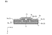
次に、本発明に係るRFIDモジュール5を備える容器1の概略構成について説明する。図1は、本発明に係る実施形態1のRFIDモジュール5を有する容器1の全体斜視図である。図2は、図1における矢視II断面図であり、図3は図1における容器1の展開図である。(Embodiment 1)
Next, a schematic configuration of the
実施形態1の容器1は、基材3と、基材3に貼り付けられたRFIDモジュール5と、基材3の第1主面3sに形成された金属膜7と、金属膜7を分断するように形成された第1スリット71とを備える。
The
容器1は、例えば、図3に示すような平面状の基材3を組み立てることで立体形状に形成される。容器1は、例えば、直方体形状であり、基材3は、例えば、紙製、樹脂製、またはプラスチック製である。
The
基材3は、第1面3a、第2面3b、第3面3c、第4面3d、第5面3e、第6面3f、及び、接合フラップ3g、第1タックフラップ3h、第2タックフラップ3k、第1ダストフラップ3m、第2ダストフラップ3n、第3ダストフラップ3p、第4ダストフラップ3q、を備える。例えば、第1面3a、第3面3c、第5面3e及び第6面3fは組み立てた際に容器1の側面となる。第4面3dは組み立てた際に容器1の上面(天面)となり、第2面3bは組み立てた際に容器1の下面(底面)となる。組み立てた際に、第1面3aと第5面3eとは対向し、第3面3cと第6面3fとが対向する。基材3の第1主面3sは主に容器1の外面(表面)となる面であり、基材3の第2主面3tは主に容器1の内面(裏面)となる面である。
The
接合フラップ3gの第1主面3sは、例えば、組み立てた際に第1面3aの第2主面3tに接着層を介して貼り付けられる。第1タックフラップ3hの第1主面3sは組み立てた際に第6面3fの第2主面3tに接触する。第2タックフラップ3kの第1主面3sは組み立てた際に第6面3fの第2主面3tに接触する。
The first
第1ダストフラップ3m及び第2ダストフラップ3nは、それぞれ、下面となる第2面3bと、側面となる第1面3a及び第5面3eとの間の隙間からゴミなどが容器1の内部に入り込むことを防止する。また、第3ダストフラップ3p及び第4ダストフラップ3qは、それぞれ、上面となる第4面3dと、側面となる第1面3a及び第5面3eとの間の隙間からゴミなどが容器1の内部に入り込むことを防止する。
The
第1面3aは下辺41を介して第1ダストフラップ3mに接続され、上辺51を介して第4ダストフラップ3qに接続される。第1スリット71は、端部から第1面3aと第1ダストフラップ3mとの境界である下辺41に沿って延び、下辺41の中央部に近づくと下辺41から離れる方向に第1ダストフラップ3m側にS字形状に折れ曲がり、さらに下辺41と平行な方向に延び、下辺41の中央部を過ぎると下辺41の方向にS字形状に折れ曲がって、再び下辺41に沿って延びる。第1面3aと第3面3cは側辺61を介して接続される。
The
第3面3cは下辺42を介して第2面3bと接続され、上辺52を介して第4面3dと接続される。下辺42に沿って第2スリット72が金属膜7に形成され、第2面3bの金属膜7と第3面3cの金属膜7とを分断している。上辺52に沿って第4スリット74が金属膜7に形成され、第3面3cの金属膜7と第4面3dの金属膜7とを分断している。容器1の展開図において、第2スリット72は、第1スリット71の延長上に位置している。
The
第2面3bは、第3面3cと反対側に第1タックフラップ3hと接続される。第2面3bと第1タックフラップ3hとの間に、第3スリット73が金属膜7に形成され、第2面3bの金属膜7と第1タックフラップ3hの金属膜7とを分断している。
The
第4面3dは、第3面3cと反対側に第2タックフラップ3kと接続される。第4面3dと第2タックフラップ3kとの間に、第5スリット75が金属膜7に形成され、第4面3dの金属膜7と第2タックフラップ3kの金属膜7とを分断している。
The
第3面3cは、第1面3aと反対側に第5面3eと接続される。第5面3eは下辺43を介して第2ダストフラップ3nに接続され、上辺53を介して第3ダストフラップ3pに接続される。第5面3eは、第3面3cと反対側に第6面3fと接続される。第6面3fは、第5面3eと反対側に接合フラップ3gと接続される。
The
金属膜7は、第1~第5スリット71~75を除いて基材3の第1主面3sの全面に形成されている。第1~第5スリット71~75は、それぞれ金属膜7を分断する溝である。金属膜7は、アルミニウム箔や銅箔などの金属箔の導電材料の膜体により作製され、例えば、金属シートを貼り付けることで形成される。金属膜7として、アルミニウムや銅などの抵抗値の小さい金属を用いることで通信距離を遠くすることができる。金属膜7の厚みは、例えば、5μmよりも大きく40μm以下である。
The
第1ダストフラップ3mの金属膜7は、第1スリット71により2つの領域に物理的に分断されている。実施形態1では、第1ダストフラップ3mの金属膜7は、第1金属領域7aと第2金属領域7bと2つの領域に分断され、第1金属領域7aと第2金属領域7bとは第1スリット71により電気的に絶縁している。なお、金属膜7は基材3の全面に形成されていなくてもよく、例えば、第1ダストフラップ3mと他の面において部分的に形成されていてもよい。
The
金属膜7は、第1スリット71から交差する方向に容器1の外側に沿って延びる第1金属領域7aと、第1スリット71から交差する方向に第1金属領域7aと反対方向に容器1の外側に沿って延びる第2金属領域7bによりダイポール型アンテナとして機能する。通信周波数の電磁波が容器1に照射されると、第1ダストフラップ3mにおいて、第1スリット71と交差する方向、例えば、直交する方向に通信周波数と共振し電流が流れる。
The
第1スリット71は、第1ダストフラップ3mの金属膜7を分断する溝である。また、第1スリット71は、第1ダストフラップ3mの第2金属領域7bの金属膜7と第1面3aの金属膜7とも分断している。第1スリット71の幅Wは、例えば、1mmである。第1スリット71は、基材3の第1主面3s全体に金属膜7を形成した後に金属膜7を削ることで形成してもよいし、2枚の金属シートを第1スリット71の幅Wを空けて基材3の第1主面3Sに貼り付けることで形成してもよい。
The
実施形態1のRFIDモジュール5は、通信周波数(キャリア周波数)を有する高周波信号で無線通信(送受信)するように構成された無線通信デバイスである。RFIDモジュール5は、例えば、UHF帯の通信用の周波数を有する高周波信号で無線通信するよう構成されている。ここでUHF帯とは、860MHzから960MHzの周波数帯域である。
The
次に、図4から図7を参照して、RFIDモジュール5の構成について説明する。図4は、RFIDモジュールの透視平面図であり、図5は、図4における矢視Vの断面図である。図6はRFIDモジュールの基板に形成されている導体パターンの平面図を示し、図6aはRFIDモジュールの基板の上面に形成された導体パターンの平面図であり、図6bは基板の下面に形成された導体パターンの上から見た透視平面図である。図7は、図4における矢視VIIの断面図である。図中において、X-Y-Z座標系は、発明の理解を容易にするものであって、発明を限定するものではない。X軸方向はRFIDモジュール5の長手方向を示し、Y軸方向は奥行き(幅)方向を示し、Z軸方向は厚さ方向を示している。X、Y、Z方向は互いに直交する。
Next, the configuration of the
図4に示すように、RFIDモジュール5は、両面テープまたは合成樹脂等の接着層15を介して金属膜7の第1金属領域7aおよび第2金属領域7bのそれぞれの上面に貼り合わされる。
As shown in FIG. 4, the
図5に示すように、RFIDモジュール5は、基板21と、基板21に搭載されるRFIC23とを備える。基板21は、例えば、ポリイミド等のフレキシブル基板である。RFIC23が実装された基板21の上面には保護膜25が形成されている。保護膜25は、例えば、ポリウレタン等のエラストマや、エチレン酢酸ビニル(EVA)のようなホットメルト剤である。基板21の下面にも、保護フィルム27が貼り付けられている。保護フィルム27は、例えば、ポリイミドフィルム(カプトンテープ)等のカバーレイフィルムである。
As shown in FIG. 5 , the
図6を参照する。基板21の上面には、第3電極33、第4電極35、第1インダクタンス素子L1の主要部の導体パターンL1a、および、第2インダクタンス素子L2の主要部の導体パターンL2aが形成されている。第3電極33は導体パターンL1aの一端と接続され、第4電極35は導体パターンL2aの一端と接続されている。これらの導体パターンは、例えば、銅箔をフォトリソグラフィによってパターニングしたものである。
Please refer to FIG. A
基板21の下面には、金属膜7の第1金属領域7aおよび第2金属領域7bにそれぞれ容量結合される第1電極29および第2電極31が形成されている。また、基板21の下面には、第1インダクタンス素子L1の一部の導体パターンL1b、第3インダクタンス素子L3の導体パターンL3a、L3b(二点鎖線で囲む導体パターン)、L3cが形成されている。これらの導体パターンも、例えば、銅箔をフォトリソグラフィによってパターニングしたものである。
A
第1インダクタンス素子L1の一部の導体パターンL1bの一端と第3インダクタンス素子L3の導体パターンL3aの一端とが第1電極29と接続されている。同様に、第2インダクタンス素子L2の導体パターンL2bの一端と第3インダクタンス素子L3の導体パターンL3cの一端とが第2電極31と接続されている。第3インダクタンス素子L3の導体パターンL3aの他端と、導体パターンL3cの他端との間には、導体パターンL3bが接続されている。
One end of the conductor pattern L1b of the first inductance element L1 and one end of the conductor pattern L3a of the third inductance element L3 are connected to the
第1インダクタンス素子L1の導体パターンL1bの他端と、第1インダクタンス素子L1の導体パターンL1aの他端とは、ビア導体V1を介して接続されている。同様に、第2インダクタンス素子L2の導体パターンL2bの他端と、第2インダクタンス素子L2の導体パターンL2aの他端とは、ビア導体V2を介して接続されている。 The other end of the conductor pattern L1b of the first inductance element L1 and the other end of the conductor pattern L1a of the first inductance element L1 are connected via a via conductor V1. Similarly, the other end of the conductor pattern L2b of the second inductance element L2 and the other end of the conductor pattern L2a of the second inductance element L2 are connected via a via conductor V2.
基板21の上面に形成された第3電極33および第4電極35にRFIC23が搭載されている。つまり、RFIC23の端子23aが第3電極33に接続されて、RFIC23の端子23bが第4電極35に接続されている。
The
第1インダクタンス素子L1と第3インダクタンス素子L3の導体パターンL3aとは、基板21の異なる層にそれぞれ形成され、かつ、それぞれのコイル開口が重なる関係に配置されている。同様に、第2インダクタンス素子L2および第3インダクタンス素子L3の導体パターンL3cとは、基板21の異なる層にそれぞれ形成され、かつ、それぞれのコイル開口が重なる関係に配置されている。さらに、RFIC23は、基板21の面上で、第2インダクタンス素子L2および第3インダクタンス素子L3の導体パターンL3cと、第1インダクタンス素子L1および第3インダクタンス素子L3の導体パターンL3aとの間に、位置する。
The conductor patterns L3a of the first inductance element L1 and the third inductance element L3 are formed in different layers of the
次に、図8を参照して、RFIDモジュール5の回路構成について説明する。図8はRFIDモジュール5の回路図である。
Next, the circuit configuration of the
RFIDモジュール5内において、基板21の上面及び下面を通る第1電流経路CP1と基板21の下面を通る第2電流経路CP2とが形成されている。第1電流経路CP1は、第1電極29から分岐点N1、導体パターンL1b、導体パターンL1a、RFIC23、導体パターンL2a、導体パターンL2b、分岐点N2、を通って第2電極31に至る。第2電流経路CP2は、第1電極29から分岐点N1、導体パターンL3a、導体パターンL3b、導体パターンL3c、分岐点N2を通って第2電極31に至る。ここで、導体パターンL1aとビア導体V1を介して接続している導体パターンL1bで構成される第1インダクタンス素子L1と、導体パターンL2aとビア導体V2を介して接続している導体パターンL2bで構成される第2インダクタンス素子L2に流れる電流の巻き方向は逆になっており、第1インダクタンス素子L1で発生する磁界と第2インダクタンス素子L2で発生する磁界はお互いに打ち消し合っている。第1電流経路CP1及び第2電流経路CP2は、それぞれ、第1電極29と第2電極31との間で、互いに並列に形成されている。
In the
RFIDモジュール5内において、第1電流経路CP1は、LC並列共振回路である並列共振回路RC1の一部であり、通信周波数の電波に対してマッチングしているので、通信周波数の電波を金属膜7が受信すると、RFIC23に電流が流れる。
In the
RFIDモジュール5は、並列共振回路RC1が形成されている。並列共振回路RC1は、第1インダクタンス素子L1、RFIC23、第2インダクタンス素子L2、および、第3インダクタンス素子L3で構成されるループ回路である。
A parallel resonant circuit RC1 is formed in the
容量C1は、第1金属領域7a、第1電極29、接着層15、および保護フィルム27で構成される。容量C2は、第2金属領域7b、第2電極31、接着層15、および保護フィルム27で構成される。第4インダクタンス素子L4は第1ダストフラップ3mの第1金属領域7a及び第1金属領域7aと電気的に接続する第1面3aの金属膜7及び第3面の金属膜7のインダクタンス成分であり、第5インダクタンス素子L5は第1ダストフラップ3mの第2金属領域7b及び第2金属領域7bと容量結合する第2面3bの金属膜7のインダクタンス成分である。
並列共振回路RC1は、通信周波数における電波に対してインピーダンス整合してLC並列共振するように設計されている。これにより、通信周波数でRFICとマッチングしており、通信周波数におけるRFIDモジュール5の通信距離を確保することができる。
The parallel resonance circuit RC1 is designed to perform LC parallel resonance by impedance matching with respect to radio waves at a communication frequency. Thereby, the communication frequency is matched with the RFIC, and the communication distance of the
図9は、実施形態1におけるRFIDモジュール5を備える容器1の通信特性を示すグラフ図である。RFIDモジュール5を備える容器1の通信特性は、860MHzから960MHzのUHF帯においても、約70cm以上の通信距離を有し、特に、920MHz付近では250cm以上の通信距離を有し、良好である。
FIG. 9 is a graph showing communication characteristics of the
実施形態1の容器1は、第4面3dと第3面3cとの間に第4スリット74と、第4面3dと第2タックフラップ3kとの間に第5スリット75が形成されている。したがって、第4面3dの金属膜7は第3面3c及び第2タックフラップ3kと電気的に直接接続されていない。これにより、図10に示すように複数の容器1を上下方向に並べた場合に、下の容器1の第4面3dと上の容器1の第2面3bとが容量結合して、下の容器1の第4面3dと上の容器1の第2面3bとが同電位となったとしても、上の容器1の第1面3a及び第3面3cの電位に影響を及ぼすのを低減することができる。したがって、それぞれの容器1の金属膜7の第1金属領域7aと第2金属領域7bとにおいて、RFIDモジュール5を経由しなければ絶縁状態が維持されているので、複数の容器1との通信を一度に行うことができる。
In the
以上のように、実施形態1の容器1は、RFIDモジュール5を備えた、組み立て式の箱形の容器1であって、容器1の外形を形成する絶縁性の基材3と、基材3上に形成された金属膜7と、金属膜7に形成された第1スリット71と、を備える。基材3は、容器1の側面となる第1面3a及び下面となる第2面3bと、第1面3aに連続した第1ダストフラップ3mと、を有する。第1スリット71は、第1ダストフラップ3mの金属膜7を第1金属領域7aと第2金属領域7bとに分離するように形成される。RFIDモジュール5は、RFIC23と、通信周波数である固有の共振周波数の電磁波による電流をRFIC23に伝送するフィルタ回路としての並列共振回路RC1と、並列共振回路RC1と接続する第1及び第2電極29、31と、を備える。RFIDモジュール5の第1電極29と第1ダストフラップ3mの金属膜7の第1金属領域7aとが電気的に接続され、RFIDモジュール5の第2電極31と第1ダストフラップ3mの金属膜7の第2金属領域7bとが電気的に接続される。第1ダストフラップ3mの金属膜7の第1金属領域7aは、第1面3aの金属膜7と連続し、組み立てられた状態において、第1ダストフラップ3mの金属膜7の第2金属領域7bは、第2面3bの金属膜7と容量結合により電気的に接続する。
As described above, the
容器1の第1ダストフラップ3mに形成された金属膜7を第1金属領域7aと第2金属領域7bとに分割する第1スリット71を跨いでRFIDモジュール5が配置されている。第1ダストフラップ3mの第1金属領域7aは第1面3aの金属膜7と連続しており、第2金属領域7bは第2面の金属膜7と容量結合している。したがって、第1及び第2金属領域7a、7bをそれぞれ、アンテナ電極として利用することができ、直列共振によりRFIC23に電流を流すことができる。この結果、金属膜7が形成された容器1であっても、無線通信が可能であり、意匠性の低減を抑制したRFIDモジュール5を有する容器1を提供することができる。
The
また、容器1において、第1面3aと連続する第1ダストフラップ3mに配置されたRFIDモジュール5は、容器1が組み立てられた状態で第2面3bの内側に位置するので、容器1の外面に現れない。したがって、容器1の意匠性が低減するのを防止することができる。
Further, in the
また、実施形態1の容器1であれば、従来の金属対応のRFIDモジュールを取り付けた容器よりも安価に提供することができる。また、従来のフラッグタイプのRFIDモジュールは容器から飛び出し、折れた場合、通信特性が悪くなる。さらには、容器から飛び出さなければならないので意匠性の自由度を低減させるが、実施形態の容器1であれば、RFIDモジュールが容器から飛び出さなくてもよいので、意匠性の自由度の低減を抑制することができる。
In addition, the
容器1は、第1面3aの金属膜7と連続する第3面3cの金属膜7と第2面3bの金属膜7とを分断する第2スリット72を備える。したがって、第2スリット72は、第1面3aの金属膜7と第2面3bの金属膜7とを電気的に分断している。これにより、通信特性を向上させることができる。
The
基材3は、第1面3a及び第2面3bとそれぞれ連続した第3面3cを有する。第2スリット72は、第2面3bの金属膜7と第3面3cの金属膜7との間に形成されている。これにより、第3面3cの金属膜7を第1金属領域7aと接続することができ、通信距離を延ばすことができる。
The
基材3は、第2面3bに対して第3面3cと反対側に、第2面3bと連続する第1タックフラップ3hを備え、第2面3bの金属膜7と第1タックフラップ3hの金属膜7との間に形成された第3スリット73を備える。これにより、第2面3bの金属膜7が、第1タックフラップ3hの金属膜7と容量結合する第6面3fの金属膜7と導通するのを防ぐことができ、通信特性が劣化するのを抑制することができる。また、容器1を組み立てられた状態で、図2に示すように、第1ダストフラップ3mの第2金属領域7bの金属膜7は第2面3bの金属膜7と基材3を介して重なるので容量結合する。これにより第2面3bの金属膜7は、第1ダストフラップ3mのブースター電極として働き、読み取り距離が向上する。なお、第1ダストフラップ3mと第2面3bとを接着層により接着してもよい。例えば、第1ダストフラップ3mに形成された金属膜7と第2面3bとを接着することで、容器1が天地逆さまになっても、第1ダストフラップ面3mの第2金属領域7bの金属膜7と第2面3bの金属膜7との容量結合を維持できるので、通信特性が劣化するのを抑制することができる。
The
金属膜7は、第1スリット71、第2スリット72及び第3スリット73を除いて基材3の全面に形成されてもよい。このように、容器1の第1主面3sのほぼ全面に金属膜7を形成する意匠も実現可能である。
The
通信周波数の電磁波が金属膜7に照射されると、第1スリット71と交差する方向に電流が流れる。このように、金属膜7はダイポールアンテナとして機能するので、ダイポールアンテナとしての通信特性を得ることができる。
When the electromagnetic wave of the communication frequency is applied to the
次に、図11を参照して実施形態1の変形例1を説明する。図11は、実施形態1の変形例1における容器1Aの展開図である。実施形態1の変形例1における容器1Aは、実施形態1の容器1の第1スリット71が第1ダストフラップ3mの先端方向にシフトした構成である。この点及び以下に説明する点以外の構成は実施形態1の容器1と実質的に同じである。
Next,
変形例1における容器1Aにおいて、第1スリット71Aが、例えば、第1ダストフラップ3mの中央部を横断するように形成されている。したがって、第1ダストフラップ3mにおける第1金属領域7aの面積が大きくなるので、第1金属領域7aが第2面3bの金属膜7と容量結合するのを防止するために、容器1Aが組み立てられた状態において、第2面3bにおける第1金属領域7aと重なる領域に非金属領域81を形成している。非金属領域81において、基材3の表面が露出してもよいし、基材3に非金属材料により塗膜してもよい。これにより、変形例1における容器1Aは、実施形態1の容器1と同様に通信することが可能である。
In the
また、第2面3bにおいて、非金属領域81と対称的に非金属領域82を形成してもよい。さらに、第4面3dにおいて、組み立てられた状態において、非金属領域81と対向する位置に非金属領域83を、非金属領域82と対向する位置に非金属領域84を、それぞれ形成してもよい。これにより、意匠性が上がると共に、容器1Aを上下方向に積み重ねた際に、容器1Aを180度回転させても非金属領域同士が重なるので、上下の容器1A間で電流が流れるのを防止することができ、まとめて無線通信することが可能である。
Also, a
次に、図12及び図13を参照して実施形態1の変形例2を説明する。図12は、実施形態1の変形例2における容器1Bの展開図である。図13は、組み立てられた容器1Bの第6面3fの正面図である。
Next, Modification 2 of
実施形態1の変形例2における容器1Bは、実施形態1の容器1において、RFIDモジュール5及び第1スリット71が第1ダストフラップ3mの代わりに第1タックフラップ3hに配置された構成である。この点及び以下に説明する点以外の構成は実施形態1の容器1と実質的に同じである。
A
容器1Bにおいて、第1ダストフラップ3mにスリットは存在しない。第2面3bの金属膜7と第1タックフラップ3hの金属膜7との間に形成された第3スリット73Bが第1タックフラップ3hの先端に向けて折れ曲げられている。したがって、第1タックフラップ3hの金属膜7は、第3スリット73Bにより、第1金属領域7a2と第2金属領域7b2に分断されている。第1金属領域7a2は、第2面3bの金属膜7と連続している。第2金属領域7b2は、組み立てられた状態で第6面3fの金属膜7と重なるので容量結合する。
In
第5面3eの金属膜7と第6面3fの金属膜7との間に、側辺に沿って第6スリット76が形成されている。また、第6面3fの金属膜7と接合フラップ3gの金属膜7との間に、側辺に沿って第7スリット77が形成されている。これにより、組み立てられた状態において、第1タックフラップ3hが第6面3fと重なり、第2金属領域7b2と第6面3fの金属膜7とを容量結合しても、第6面3fの金属膜7の電位が第5面3eの金属膜7の電位及び接合フラップ3gの金属膜7の電位により影響されるのを低減することができる。したがって、第6面3fの金属膜7をアンテナ素子として利用することができる。
A
第1タックフラップ3hの第1金属領域7a2が第6面3fの金属膜7と容量結合するのを防止するために、容器1Bが組み立てられた状態において、第6面3fにおける第1金属領域7a2と重なる領域に非金属領域85を形成している。非金属領域85は、第7スリット77と接続されている。非金属領域85において、基材3の表面が露出してもよいし、基材3に非金属材料により塗膜してもよい。
In order to prevent capacitive coupling of the first metal region 7a2 of the
このように、基材3は、第1フラップとしての第1タックフラップ3hの反対側に、第1面としての第2面3bと連続する第3面3cと、第2面としての第6面3fと第3面3cとの間に位置し、第6面3fおよび第3面3cとそれぞれ連続する第4面としての第5面3eと、第5面3eと反対側に、第6面3fと連続する接合フラップ3fと、を備える。第6面3fの金属膜7と第5面3eの金属膜7との間に第2スリットとしての第6スリット76が形成されている。第6面3fの金属膜7と接合フラップ3gの金属膜7との間にそれぞれの金属膜7を分離する第3スリットとしての第7スリット77が形成されている。組み立てられた状態において、第6面3fと第3面3cとが対向し、第1タックフラップ3hの金属膜7の第1金属領域7a2と重なる第6面3fの非金属領域85に金属膜7が形成されていない。
Thus, the
このような構成によっても、実施形態1の容器1と同様に通信することができる。また、RFIDモジュール5が第1タックフラップ3h上に配置されているので、組み立てられた状態において、第6面3fの内側に位置するので、容器1の外面に現れない。したがって、容器1の意匠性が低減するのを防止することができる。
Even with such a configuration, communication can be performed in the same manner as the
次に、図14及び図15を参照して実施形態1の変形例3を説明する。図14は、実施形態1の変形例3における容器1Cの展開図である。図15は、組み立てられた容器1Cの第6面3fの正面図である。
Next,
実施形態1の変形例3における容器1Cは、実施形態1の変形例2の容器1Bにおいて、第1金属領域7a2を第6面3fと容量結合させた構成である。この点及び以下に説明する点以外の構成は実施形態1の変型例2の容器1Bと実質的に同じである。
A
第1タックフラップ3hの金属膜7は、スリット73Cにより、第1金属領域7a3と第2金属領域7b3に分断されている。第1金属領域7a3は、第2面3bの金属膜7と連続している。第1金属領域7a3は、組み立てられた状態で第6面3fの金属膜7と重なるので容量結合する。
The
第1タックフラップ3hの第2金属領域7b3が第6面3fの金属膜7と容量結合するのを防止するために、容器1Cが組み立てられた状態において、第6面3fにおける第2金属領域7b3と重なる領域に非金属領域86を形成している。非金属領域86において、基材3の表面が露出してもよいし、基材3に非金属材料により塗膜してもよい。
In order to prevent the second metal region 7b3 of the
このように、基材3は、第1フラップとしての第1タックフラップ3hの反対側に、第1面としての第2面3bと連続する第3面3cと、第2面としての第6面3fと第3面3cとの間に位置し、第6面3fおよび第3面3cとそれぞれ連続する第4面としての第5面3eとを備える。組み立てられた状態において、第6面3fと第3面3cとが対向し、第1タックフラップ3hの金属膜7の第2金属領域7b3と重なる第6面3fの非金属領域86に金属膜7が形成されていない。
Thus, the
このような構成によっても、実施形態1の容器1と同様に通信することができる。また、RFIDモジュール5が第1タックフラップ3h上に配置されているので、容器1Cが組み立てられた状態において、第6面3fの内側に位置するので、容器1の外面に現れない。したがって、容器1の意匠性が低減するのを防止することができる。
Even with such a configuration, communication can be performed in the same manner as the
次に、図16を参照して実施形態1の変形例4を説明する。図16は、実施形態1の変形例3における容器1Dの展開図である。
Next, Modification 4 of
実施形態1の変形例4における容器1Dは、実施形態1の容器1においてRFIDモジュール5が第1ダストフラップ3mに配置されていた代わりに、RFIDモジュール5が接合フラップ3gdの本体フラップ3gdaから延びる延伸フラップ3gdbに配置された構成である。この点及び以下に説明する点以外の構成は実施形態1の容器1と実質的に同じである。
In the
容器1Dの接合フラップ3gdは、本体フラップ3gdaと、本体フラップ3gdaから延びる延伸フラップ3gdbを備える。本体フラップ3gdaは、実施形態1の接合フラップ3gに相当する。本体フラップ3gda上に第1金属領域7a4が配置されている。延伸フラップ3gdbは、容器1Dを組み立てる際に、接合フラップ3gaとの接続線に沿って折り曲げられて、第4面3dの内側に重なるように配置される。延伸フラップ3gdbには、金属膜7が形成され、第2金属領域7b4が配置されている。延伸フラップ3gdbは、接合フラップ3ga側に第1スリット71が形成されている。
The joining flap 3gd of the
変形例4において、第1タックフラップ3h、第2タックフラップ3k、第1ダストフラップ3m~第4ダストフラップ3qの第1主面3s上にはそれぞれ金属膜7が形成されていない。これらのフラップは、容器1Dが組み立てられた状態では外部に露出しないので、金属膜7が形成されていなくても意匠性を損なうことはない。また、これらのフラップに金属膜7を形成しないことでコストダウンすることもできる。
In Modification 4, the
第1面3a、第3面3c、第5面3e、第6面3f、及び、接合フラップ3gの本体フラップ3gに形成されたそれぞれの金属面7は連続しており、導通している。第2面3bと第3面3cとの間に第2スリット72が形成され、第4面3dと第3面3cとの間に第4スリット74が形成されている。したがって、第2面3b及び第3面3cのそれぞれに形成された金属膜7は、分断され、互いに導通していない。また、第4面3d及び第3面3cのそれぞれに形成された金属膜7も、分断され、互いに導通していない。
The metal surfaces 7 formed on the
第5面3eにおける、第2ダストフラップ3nと第4ダストフラップ3qとの間の側辺の高さLaは、例えば、5cmであり、第5面3e及び第6面3fのそれぞれの横方向の長さLb、Lcが、例えば、6cmである場合、容器1Dの高さが低いので、容器1Dの側面の金属膜7の長さでは通信距離が短くなる。いずれかのフラップにスリットを形成してもフラップの高さは側面の縦横のそれぞれの長さの半分までしかできないので、この場合、最長3cmしか伸ばせない。
The height La of the side between the
これに対して、延伸フラップ3gdbを用いる場合、金属膜7の長さLeは、第4面3d及び第6面3fの長さLcと同じにすることができるので、最長6cmまでアンテナ電極として延ばすことができる。これにより、接合フラップ3gaの金属膜7と合わせて長さLcが最大約11cmまで確保することができ、通信距離を向上させることができる。
On the other hand, when the extension flap 3gdb is used, the length Le of the
このように、基材3は、容器1Dの側面、天面、及び底面のいずれかとなる第1面としての第6面3f及び第2面としての第4面3dと、第6面3fに連続した第1フラップとしての接合フラップ3gdと、を有する。第1スリット71は、接合フラップ3gdの金属膜7を第1金属領域7a4と第2金属領域7b4とに分離するように形成される。RFIDモジュール5の第1電極29と接合フラップ3gdの金属膜7の第1金属領域7a4とが電気的に接続され、RFIDモジュール5の第2電極31と接合フラップ3gdの金属膜7の第2金属領域7b4とが電気的に接続される。接合フラップ3gdの金属膜7の第1金属領域7a4は、第6面3fの金属膜7と連続し、組み立てられた状態において、接合フラップ3gdの延伸フラップ3gdb上の第2金属領域7b4は、第4面3dの金属膜7と容量結合により電気的に接続する。このような構成によっても、実施形態1の容器1と同様に通信することができる。
In this way, the
容器1を組み立てる際に、接合フラップ3gdの本体フラップ3gdaに対向する第1面3aの裏側に接着層を塗って本体フラップ3gdaを第1面3aの裏側に貼り合わせることで、本体フラップ3gdaから延伸された貼り合わせない延伸フラップ3gdbがあっても簡単に接着し容器1の形成をすることができる。またRFIDモジュール5は延伸フラップ3gdbに貼着されており、その位置は第4ダストフラップ3qに重なる位置になるので、接合フラップ3gdbと第4ダストフラップ3qを貼り合わせると、RFIDモジュール5は接合フラップ3gdbと第4ダストフラップ3qの間に挟まれる状態になる。この為、第4ダストフラップ3qはRFIDモジュール5を保護するように配置される。これにより容器1同士が擦れることにより、RFIDモジュール5にせん断応力がかかることを防ぐので、RFIDモジュール5の脱落を防ぐ。また容器1に内容物を入れる時にも、内容物や手が接触することによるRFIDモジュール5の脱落を防ぐことが出来る。
When assembling the
(実施形態2)
以下、本発明に係る実施形態2の容器1について説明する。(Embodiment 2)
A
実施形態2の容器1と実施形態1の容器1との相違点は、金属膜7のシート抵抗の違いである。この相違点を中心に以下に説明する。なお、実施形態2の説明において、前述の実施形態1と同様の構成、作用および機能を有する要素に対しては重複する記載を避けるため説明を省略する場合がある。実施形態2の容器1は、以下に説明する点以外の構成については、実施形態1のRFIDモジュール5と同様の構成である。
The difference between the
実施形態2の容器1の金属膜7のシート抵抗は、実施形態1の容器1の金属膜7のシート抵抗よりも大きい。金属膜7のシート抵抗が大きい場合、実施形態1の容器1では発生しなかった以下の問題が発生する。
The sheet resistance of the
実施形態1の容器1では、アンテナ電極として金属膜7の全体で共振現象を起こし、電磁波を放射していた。実施形態1における金属膜7の厚みは、例えば、5μmより大きく40μm以下であり、金属膜7のシート抵抗では、0.05Ω/□以下である。
In the
容器の金属膜は、通常、食品酸化防止や意匠性の向上のために形成されているが、金属膜の厚みが、例えば、5μmのようにμm単位の1桁の数値の場合でも、その上に、意匠としてグラビア印刷またはオフセット印刷等で印刷すると、印刷厚みが1μm程度になる。この場合、印刷物にアンテナ箔としての金属膜の厚みによる段差が発生し、これにより印刷ズレ(かすれ、または、にじみ)が発生する。このような理由により、従来のアンテナ箔が貼ってある容器に意匠として直接印刷することが出来なかった。 The metal film of the container is usually formed to prevent food oxidation and improve design. Furthermore, if the design is printed by gravure printing, offset printing, or the like, the printing thickness will be about 1 μm. In this case, a difference in level occurs in the printed matter due to the thickness of the metal film as the antenna foil, which causes printing misalignment (blurring or bleeding). For these reasons, it has not been possible to directly print a design on a container to which a conventional antenna foil is attached.
アンテナとしての金属膜を蒸着法により形成する場合、金属膜の厚みは、さらに小さく、10Å(=1nm)~10000Å(=1μm)程度になる。金属膜がこの程度の厚みであれば、その上にグラビア印刷をしても段差による印刷じみは発生しないが、この厚みの金属膜(蒸着膜)、例えば、アルミ箔は、膜厚が小さいのでシート抵抗が大きくなり、例えば、0.5Ω~50Ω/□程度になる。 When a metal film as an antenna is formed by vapor deposition, the thickness of the metal film is even smaller, about 10 Å (=1 nm) to 10000 Å (=1 μm). If the metal film is of this thickness, even if gravure printing is performed on it, print bleeding due to steps will not occur. Sheet resistance increases, for example, about 0.5Ω to 50Ω/□.
金属膜のシート抵抗が大きくなると、金属膜によるアンテナ電極全体で定在波を作る直列共振現象を起こしても、金属箔の抵抗により放射電力が、ほとんど熱になってしまうので、アンテナとして電磁波放射を行うことができない。 If the sheet resistance of the metal film increases, even if a series resonance phenomenon that creates a standing wave occurs in the entire antenna electrode of the metal film, the radiated power will be mostly heat due to the resistance of the metal foil. cannot be done.
また、RFICとアンテナ間のマッチング回路部の抵抗値も金属膜と同じ厚みになってしまうので、整合回路部の抵抗値が上昇し、整合ロスが大きくなり、RFIDモジュールとして動作しない。 In addition, since the resistance value of the matching circuit section between the RFIC and the antenna has the same thickness as the metal film, the resistance value of the matching circuit section increases, the matching loss increases, and the RFID module does not operate.
このように、膜厚の薄い金属膜によるアンテナ電極では(直列)共振現象による電磁波放射を起こすことができないが、金属膜で電磁波を受けると、金属膜に電磁波を打ち消すように電流が流れて電磁波をシールドする。この電流は、渦電流とも呼ばれる。渦電流が流れると、金属膜に流れる電流成分は、アンテナ電極の共振現象によるものではないので電極パターン形状に寄らず全周波数成分に対応することができる。この渦電流は、金属シールドの効果としては知られているが、通常はアンテナとして利用されていない。 In this way, an antenna electrode made of a thin metal film cannot emit electromagnetic waves due to a (series) resonance phenomenon. to shield. This current is also called eddy current. When the eddy current flows, the current component flowing in the metal film is not due to the resonance phenomenon of the antenna electrode, so it can handle all frequency components regardless of the electrode pattern shape. This eddy current is known as an effect of metal shielding, but it is not commonly used as an antenna.
RFIDモジュール5には、固有の共振周波数の電流だけをRFIC23に伝送するフィルタ回路としての並列共振回路RC1を有するので、渦電流が周波数選択されてRFIC23に電流が流れてエネルギーが伝送される。アンテナ電極としての金属膜7とRFIDモジュール5間で特定周波数だけを選択して、インピーダンス整合し、RFIC23と金属膜7間のエネルギー伝達が可能となる。このようにして、RFIC23と通信可能になると考えられる。
Since the
したがって、実施形態2の容器1であれば、金属膜7のシート抵抗が高い場合でも、従来では利用されなかった渦電流を用いることで通信可能にすることができる。
Therefore, with the
また、金属膜7の面抵抗値が高い状態は、金属膜7の厚みだけでなく金属膜7の製法によっても発生する。例えば、金属膜7を導電性ペーストにより形成する場合も、シート抵抗が0.5Ω以上になる場合がある。このような場合でも、実施形態2の容器1であれば、無線通信を行うことができる。
Moreover, the high surface resistance value of the
本発明は、上記各実施の形態のものに限らず、次のように変形実施することができる。 The present invention is not limited to the above embodiments, and can be modified as follows.
(1)上記各実施の形態において、接合フラップ3gが第1面3aに接着されていたがこれに限らない。第1タックフラップ3h、第2タックフラップ3k、第1ダストフラップ3m~第4ダストフラップ3qの任意のフラップが重なる面と接着してもよい。また、接合フラップ3gが第1面3aに接着されなくてもいい。
(1) In each of the embodiments described above, the joining
(2)上記各実施の形態において、容器1は組み立て式であったがこれに限らない。容器1は、瓶またはペットボトルであってもよい。
(2) In each of the embodiments described above, the
(3)上記各実施の形態において、通信用周波数帯はUHF帯であったがこれに限られない。HF帯の通信用の周波数(キャリア周波数)を有する高周波信号で無線通信するよう構成されていてもよい。この場合、第1スリット71に対して直交する金属膜7の全長がHF帯の高周波信号を受信するように設計される。なお、HF帯とは、13MHz以上15MHz以下の周波数帯域である。
(3) In each of the above embodiments, the communication frequency band is the UHF band, but it is not limited to this. It may be configured to perform wireless communication using a high-frequency signal having a frequency (carrier frequency) for communication in the HF band. In this case, the entire length of the
(4)上記各実施の形態において、RFIDモジュール5が金属膜7に貼られていたが、これに限らない。RFIC23を、インダクタを介して金属膜7に電気的に接続してもよい。この場合、インダクタはアンテナパターンとして機能する金属膜7側に形成される。インダクタを金属膜7側に形成する場合、金属膜7は、実施形態1のように金属箔を貼り付けることでシート抵抗を低くしてもよい。
(4) In each of the embodiments described above, the
(5)上記各実施の形態において、金属膜7において、RFIDモジュール5が貼り付けられている箇所以外の領域上に塗料を塗布して模様を形成し、容器1の意匠性を高めてもよい。また、金属膜7及びスロット9は、基材3の外面となる第1主面3Sの代わりに内面となる第2主面3t上に形成してもよい。
(5) In each of the above-described embodiments, the design of the
本発明をある程度の詳細さをもって各実施の形態において説明したが、これらの実施の形態の開示内容は構成の細部において変化してしかるべきものであり、各実施の形態における要素の組合せや順序の変化は請求された本発明の範囲および思想を逸脱することなく実現し得るものである。 Although the present invention has been described in each embodiment with a certain degree of detail, the disclosure of these embodiments should vary in details of construction, and the combination and order of elements in each embodiment may vary. Changes may be made without departing from the scope and spirit of the claimed invention.
1 容器
3 基材
3a 第1面
3b 第2面
3c 第3面
3d 第4面
3e 第5面
3f 第6面
3g 接合フラップ
3h 第1タックフラップ
3k 第2タックフラップ
3m 第1ダストフラップ
3n 第2ダストフラップ
3p 第3ダストフラップ
3q 第4ダストフラップ
3s 第1主面
3t 第2主面
5 RFIDモジュール
5a 表面
5b 裏面
7 金属膜
7a、7a2 第1金属領域
7b、7b2 第2金属領域
15 接着層
21 モジュール基板
23 RFIC
23a 端子
23b 端子
25 保護膜
27 保護フィルム
29 第1電極
31 第2電極
33 第3電極
35 第4電極
37、39 導体パターン
41、43、45、47 下辺
51、53、55、57 上辺
61 側辺
71 第1スリット
72 第2スリット
73、73B 第3スリット
74 第4スリット
75 第5スリット
76 第6スリット
77 第7スリット
81、82、83、84、85 非金属領域
L1 第1インダクタンス素子
L1a 導体パターン
L2a 導体パターン
L2 第2インダクタンス素子
L2a 導体パターン
L2b 導体パターン
L3 第3インダクタンス素子
L3a 導体パターン
L3b 導体パターン
L3c 導体パターン
L4 第4インダクタンス素子
L5 第5インダクタンス素子
Lg1 距離
Lg2 距離
CL 中心線
CP1 第1電流経路
CP2 第2電流経路
C1 容量
C2 容量1
7a, 7a2
Claims (15)
前記容器の外形を形成する絶縁性の基材と、
前記基材上に形成された金属膜と、
前記金属膜に形成された第1スリットと、を備え、
前記基材は、
前記容器の側面、天面、及び底面のいずれかとなる第1面及び第2面と、
前記第1面に連続した第1フラップと、を有し、
前記第1スリットは、前記第1フラップの前記金属膜を第1金属領域と第2金属領域とに分離するように形成され、
前記RFIDモジュールは、
RFIC素子と、
通信周波数である固有の共振周波数の電磁波による電流を前記RFIC素子に伝送するフィルタ回路と、
前記フィルタ回路と接続する第1及び第2電極と、を備え、
前記RFIDモジュールの前記第1電極と前記第1フラップの前記金属膜の前記第1金属領域とが電気的に接続され、
前記RFIDモジュールの前記第2電極と前記第1フラップの前記金属膜の前記第2金属領域とが電気的に接続され、
前記第1フラップの前記金属膜の前記第1金属領域は、前記第1面の前記金属膜と連続し、
組み立てられた状態において、前記第1フラップの前記金属膜の前記第2金属領域は、前記第2面の前記金属膜と容量結合により電気的に接続する、
RFIDモジュールを備えた容器。A collapsible box-shaped container with an RFID module, comprising:
an insulating base material forming the outer shape of the container;
a metal film formed on the substrate;
and a first slit formed in the metal film,
The base material is
a first surface and a second surface that are one of the side surface, the top surface, and the bottom surface of the container;
a first flap continuous with the first surface;
the first slit is formed to separate the metal film of the first flap into a first metal region and a second metal region;
The RFID module is
an RFIC element;
a filter circuit that transmits a current due to electromagnetic waves having a unique resonance frequency, which is a communication frequency, to the RFIC element;
first and second electrodes connected to the filter circuit,
the first electrode of the RFID module and the first metal region of the metal film of the first flap are electrically connected;
the second electrode of the RFID module and the second metal region of the metal film of the first flap are electrically connected;
the first metal region of the metal film of the first flap is continuous with the metal film of the first surface;
in an assembled state, the second metal region of the metal film of the first flap is electrically connected to the metal film of the second surface by capacitive coupling;
Container with RFID module.
請求項1に記載のRFIDモジュールを備えた容器。a second slit separating the metal film on the first surface and the metal film on the second surface;
A container provided with the RFID module according to claim 1 .
前記第2スリットは、前記第2面の前記金属膜と前記第3面の前記金属膜との間に形成されている、
請求項2に記載のRFIDモジュールを備えた容器。the base material has a third surface that is continuous with the first surface and the second surface, respectively;
The second slit is formed between the metal film on the second surface and the metal film on the third surface,
A container comprising the RFID module according to claim 2.
前記第2面の前記金属膜と前記第1タックフラップの前記金属膜との間に形成された第3スリットを備える、
請求項3に記載のRFIDモジュールを備えた容器。The base material has a first tack flap continuous with the second surface on the side opposite to the third surface,
a third slit formed between the metal film on the second surface and the metal film on the first tuck flap;
A container comprising the RFID module according to claim 3.
請求項4に記載のRFIDモジュールを備えた容器。The metal film is formed on the entire surface of the base material except for the first slit, the second slit, and the third slit,
A container comprising the RFID module according to claim 4.
請求項4に記載のRFIDモジュールを備えた容器。In the assembled state, the metal film is not formed on a region of the second surface that overlaps the first metal region of the metal film of the first flap.
A container comprising the RFID module according to claim 4.
前記基材は、前記第3面と反対側に、前記第4面と連続する第2タックフラップと、
前記第3面の前記金属膜と前記第4面の前記金属膜との間に形成された第4スリットと、
前記第4面の前記金属膜と前記第2タックフラップの前記金属膜との間に形成された第5スリットと、を備える、
請求項4から6のいずれか1つに記載のRFIDモジュールを備えた容器。The substrate has a fourth surface continuous with the third surface on the side opposite to the second surface,
The base material has a second tuck flap continuous with the fourth surface on the side opposite to the third surface,
a fourth slit formed between the metal film on the third surface and the metal film on the fourth surface;
a fifth slit formed between the metal film on the fourth surface and the metal film on the second tuck flap;
A container provided with the RFID module according to any one of claims 4 to 6.
前記第1フラップと反対側に、前記第1面と連続する第3面と、
前記第2面と前記第3面との間に位置し、前記第2面および前記第3面とそれぞれ連続する第4面と、
前記第4面と反対側に、前記第2面と連続する接合フラップと、を備え、
前記第2面の前記金属膜と前記第4面の前記金属膜との間に前記第2スリットが形成され、
前記第2面の金属膜と前記接合フラップの前記金属膜との間にそれぞれの金属膜を分離する第3スリットが形成され、
組み立てられた状態において、前記第2面と前記第3面とが対向し、前記第1フラップの前記金属膜の前記第1金属領域と重なる前記第2面の領域に前記金属膜が形成されていない、
請求項2に記載のRFIDモジュールを備えた容器。The base material is
a third surface, opposite to the first flap, continuous with the first surface;
a fourth surface positioned between the second surface and the third surface and continuous with the second surface and the third surface;
a joining flap that is continuous with the second surface on the side opposite to the fourth surface;
the second slit is formed between the metal film on the second surface and the metal film on the fourth surface;
a third slit is formed between the metal film of the second surface and the metal film of the joining flap, separating each metal film;
In the assembled state, the second surface and the third surface face each other, and the metal film is formed in a region of the second surface that overlaps the first metal region of the metal film of the first flap. No,
A container comprising the RFID module according to claim 2.
前記第1フラップと反対側に、前記第1面と連続する第3面と、
前記第2面と前記第3面との間に位置し、前記第2面および前記第3面とそれぞれ連続する第4面とを備え、
組み立てられた状態において、前記第2面と前記第3面とが対向し、前記第1フラップの前記金属膜の前記第2金属領域と重なる前記第2面の領域に前記金属膜が形成されていない、
請求項2に記載のRFIDモジュールを備えた容器。The base material is
a third surface, opposite to the first flap, continuous with the first surface;
a fourth surface positioned between the second surface and the third surface and continuous with the second surface and the third surface;
In the assembled state, the second surface and the third surface face each other, and the metal film is formed in a region of the second surface that overlaps the second metal region of the metal film of the first flap. No,
A container comprising the RFID module according to claim 2.
請求項8または9に記載のRFIDモジュールを備えた容器。The first flap is a tuck flap,
A container comprising the RFID module according to claim 8 or 9.
前記第1面と接続する本体フラップと、
前記本体フラップから延伸する延伸フラップと、を有し、
前記本体フラップ上に前記第1金属領域が配置され、
前記延伸フラップ上に前記第2金属領域が配置される、
請求項1に記載のRFIDモジュールを備えた容器。The first flap is
a body flap that connects with the first surface;
an extension flap extending from the body flap,
said first metal region disposed on said body flap;
the second metal region is positioned on the stretch flap;
A container provided with the RFID module according to claim 1 .
請求項1から11のいずれか1つに記載のRFIDモジュールを備えた容器。When the metal film is irradiated with an electromagnetic wave having a communication frequency, a current flows in a direction intersecting with the first slit.
A container provided with an RFID module according to any one of claims 1-11.
請求項1から12のいずれか1つに記載のRFIDモジュールを備えた容器。wherein the filter circuit is an LC parallel resonant circuit,
A container provided with an RFID module according to any one of claims 1-12.
請求項1から13のいずれか1つに記載のRFIDモジュールを備えた容器。The sheet resistance of the metal film is 0.5Ω/□ or more.
A container provided with an RFID module according to any one of claims 1-13.
請求項14に記載のRFIDモジュールを備えた容器。The thickness of the metal film is 1 nm or more and 1 μm or less.
A container comprising the RFID module according to claim 14.
Applications Claiming Priority (3)
| Application Number | Priority Date | Filing Date | Title |
|---|---|---|---|
| JP2021008975 | 2021-01-22 | ||
| JP2021008975 | 2021-01-22 | ||
| PCT/JP2022/002261 WO2022158579A1 (en) | 2021-01-22 | 2022-01-21 | Container provided with rfid module |
Publications (2)
| Publication Number | Publication Date |
|---|---|
| JPWO2022158579A1 JPWO2022158579A1 (en) | 2022-07-28 |
| JP7197065B2 true JP7197065B2 (en) | 2022-12-27 |
Family
ID=82548812
Family Applications (1)
| Application Number | Title | Priority Date | Filing Date |
|---|---|---|---|
| JP2022548065A Active JP7197065B2 (en) | 2021-01-22 | 2022-01-21 | Container with RFID module |
Country Status (3)
| Country | Link |
|---|---|
| US (1) | US20230359847A1 (en) |
| JP (1) | JP7197065B2 (en) |
| WO (1) | WO2022158579A1 (en) |
Citations (3)
| Publication number | Priority date | Publication date | Assignee | Title |
|---|---|---|---|---|
| WO2009004827A1 (en) | 2007-07-04 | 2009-01-08 | Murata Manufacturing Co., Ltd. | Wireless ic device |
| CN102372120A (en) | 2010-08-16 | 2012-03-14 | 姜文波 | Metal foil paper capable of being used as RFID label and manufacturing method thereof and packaging box |
| JP7074275B1 (en) | 2020-11-09 | 2022-05-24 | 株式会社村田製作所 | Container with RFID module |
Family Cites Families (2)
| Publication number | Priority date | Publication date | Assignee | Title |
|---|---|---|---|---|
| JP5028176B2 (en) * | 2007-07-25 | 2012-09-19 | 株式会社日立製作所 | RFID tag mounting package and manufacturing method thereof |
| JP2022056014A (en) * | 2020-09-29 | 2022-04-08 | 大日本印刷株式会社 | Packaging container with RF tag |
-
2022
- 2022-01-21 JP JP2022548065A patent/JP7197065B2/en active Active
- 2022-01-21 WO PCT/JP2022/002261 patent/WO2022158579A1/en active Application Filing
-
2023
- 2023-07-20 US US18/355,868 patent/US20230359847A1/en active Pending
Patent Citations (3)
| Publication number | Priority date | Publication date | Assignee | Title |
|---|---|---|---|---|
| WO2009004827A1 (en) | 2007-07-04 | 2009-01-08 | Murata Manufacturing Co., Ltd. | Wireless ic device |
| CN102372120A (en) | 2010-08-16 | 2012-03-14 | 姜文波 | Metal foil paper capable of being used as RFID label and manufacturing method thereof and packaging box |
| JP7074275B1 (en) | 2020-11-09 | 2022-05-24 | 株式会社村田製作所 | Container with RFID module |
Also Published As
| Publication number | Publication date |
|---|---|
| JPWO2022158579A1 (en) | 2022-07-28 |
| WO2022158579A1 (en) | 2022-07-28 |
| US20230359847A1 (en) | 2023-11-09 |
Similar Documents
| Publication | Publication Date | Title |
|---|---|---|
| US7652636B2 (en) | RFID devices having self-compensating antennas and conductive shields | |
| JP6583589B2 (en) | Wireless communication device | |
| JP7074275B1 (en) | Container with RFID module | |
| WO2012005278A1 (en) | Antenna and rfid device | |
| US20140292586A1 (en) | Antenna device, rfid tag, and communication terminal apparatus | |
| US7857230B2 (en) | Wireless IC device and manufacturing method thereof | |
| US10970610B2 (en) | RFIC module and RFID tag | |
| JP6590122B1 (en) | RFID tag and article to which RFID tag is attached | |
| EP1614192B1 (en) | Rfid devices having self-compensating antennas and conductive shields | |
| WO2012093541A1 (en) | Wireless communication device | |
| JP2021522572A (en) | How to use a shielded RFID strap with RFID tag design | |
| JP5655602B2 (en) | Antenna and RFID device | |
| US11100382B2 (en) | Card-type wireless communication device | |
| EP2309597A1 (en) | RFID devices having self-compensating antennas and conductive shields | |
| JP7197065B2 (en) | Container with RFID module | |
| JP7239073B2 (en) | Container with RFID module | |
| WO2022097682A1 (en) | Container provided with rfid module | |
| US20230259735A1 (en) | Container provided with rfid module and method for manufacturing container provided with rfid module | |
| JP7294562B2 (en) | Container with RFID module | |
| JP7095827B2 (en) | RFID auxiliary antenna device | |
| JP7133228B2 (en) | RF tag and RF tag device | |
| JP5427252B2 (en) | IC tag and manufacturing method thereof | |
| JPWO2019031534A1 (en) | RF tag antenna and RF tag |
Legal Events
| Date | Code | Title | Description |
|---|---|---|---|
| A621 | Written request for application examination |
Free format text: JAPANESE INTERMEDIATE CODE: A621 Effective date: 20220805 |
|
| A871 | Explanation of circumstances concerning accelerated examination |
Free format text: JAPANESE INTERMEDIATE CODE: A871 Effective date: 20220805 |
|
| TRDD | Decision of grant or rejection written | ||
| A01 | Written decision to grant a patent or to grant a registration (utility model) |
Free format text: JAPANESE INTERMEDIATE CODE: A01 Effective date: 20221115 |
|
| A61 | First payment of annual fees (during grant procedure) |
Free format text: JAPANESE INTERMEDIATE CODE: A61 Effective date: 20221128 |
|
| R150 | Certificate of patent or registration of utility model |
Ref document number: 7197065 Country of ref document: JP Free format text: JAPANESE INTERMEDIATE CODE: R150 |