WO2022097682A1 - Container provided with rfid module - Google Patents
Container provided with rfid module Download PDFInfo
- Publication number
- WO2022097682A1 WO2022097682A1 PCT/JP2021/040609 JP2021040609W WO2022097682A1 WO 2022097682 A1 WO2022097682 A1 WO 2022097682A1 JP 2021040609 W JP2021040609 W JP 2021040609W WO 2022097682 A1 WO2022097682 A1 WO 2022097682A1
- Authority
- WO
- WIPO (PCT)
- Prior art keywords
- container
- rfid module
- metal film
- slot
- rfid
- Prior art date
Links
- 229910052751 metal Inorganic materials 0.000 claims abstract description 122
- 239000002184 metal Substances 0.000 claims abstract description 122
- 238000004891 communication Methods 0.000 claims abstract description 60
- 239000000463 material Substances 0.000 claims abstract description 35
- 239000000758 substrate Substances 0.000 claims description 27
- 239000011241 protective layer Substances 0.000 claims description 3
- 239000010408 film Substances 0.000 description 114
- 239000004020 conductor Substances 0.000 description 65
- 230000004048 modification Effects 0.000 description 20
- 238000012986 modification Methods 0.000 description 20
- 230000008859 change Effects 0.000 description 14
- 238000013461 design Methods 0.000 description 13
- 230000001681 protective effect Effects 0.000 description 10
- 239000011888 foil Substances 0.000 description 7
- 238000011161 development Methods 0.000 description 5
- 230000000694 effects Effects 0.000 description 5
- 230000005855 radiation Effects 0.000 description 5
- 230000009467 reduction Effects 0.000 description 5
- RYGMFSIKBFXOCR-UHFFFAOYSA-N Copper Chemical compound [Cu] RYGMFSIKBFXOCR-UHFFFAOYSA-N 0.000 description 4
- 238000007639 printing Methods 0.000 description 4
- 239000000853 adhesive Substances 0.000 description 3
- 230000001070 adhesive effect Effects 0.000 description 3
- 239000012790 adhesive layer Substances 0.000 description 3
- 229910052782 aluminium Inorganic materials 0.000 description 3
- XAGFODPZIPBFFR-UHFFFAOYSA-N aluminium Chemical compound [Al] XAGFODPZIPBFFR-UHFFFAOYSA-N 0.000 description 3
- 239000011889 copper foil Substances 0.000 description 3
- 238000005452 bending Methods 0.000 description 2
- 230000000740 bleeding effect Effects 0.000 description 2
- 238000010586 diagram Methods 0.000 description 2
- 238000007646 gravure printing Methods 0.000 description 2
- 239000010410 layer Substances 0.000 description 2
- 239000007788 liquid Substances 0.000 description 2
- 238000000206 photolithography Methods 0.000 description 2
- 229920001721 polyimide Polymers 0.000 description 2
- 239000011347 resin Substances 0.000 description 2
- 229920005989 resin Polymers 0.000 description 2
- 239000004642 Polyimide Substances 0.000 description 1
- 239000004820 Pressure-sensitive adhesive Substances 0.000 description 1
- 230000005540 biological transmission Effects 0.000 description 1
- 239000003795 chemical substances by application Substances 0.000 description 1
- 229910052802 copper Inorganic materials 0.000 description 1
- 239000010949 copper Substances 0.000 description 1
- 230000008878 coupling Effects 0.000 description 1
- 238000010168 coupling process Methods 0.000 description 1
- 238000005859 coupling reaction Methods 0.000 description 1
- 239000012787 coverlay film Substances 0.000 description 1
- 239000003989 dielectric material Substances 0.000 description 1
- 229920001971 elastomer Polymers 0.000 description 1
- 239000000806 elastomer Substances 0.000 description 1
- 230000005672 electromagnetic field Effects 0.000 description 1
- 238000005516 engineering process Methods 0.000 description 1
- 239000005038 ethylene vinyl acetate Substances 0.000 description 1
- 230000004907 flux Effects 0.000 description 1
- 239000012943 hotmelt Substances 0.000 description 1
- 238000004519 manufacturing process Methods 0.000 description 1
- 239000007769 metal material Substances 0.000 description 1
- 238000000034 method Methods 0.000 description 1
- 238000007645 offset printing Methods 0.000 description 1
- 230000003647 oxidation Effects 0.000 description 1
- 238000007254 oxidation reaction Methods 0.000 description 1
- 239000003973 paint Substances 0.000 description 1
- 239000000123 paper Substances 0.000 description 1
- 230000003071 parasitic effect Effects 0.000 description 1
- 239000004033 plastic Substances 0.000 description 1
- 229920003023 plastic Polymers 0.000 description 1
- 229920003223 poly(pyromellitimide-1,4-diphenyl ether) Polymers 0.000 description 1
- 229920002635 polyurethane Polymers 0.000 description 1
- 239000004814 polyurethane Substances 0.000 description 1
- 238000007790 scraping Methods 0.000 description 1
- 238000004904 shortening Methods 0.000 description 1
- 238000009751 slip forming Methods 0.000 description 1
- 229920003002 synthetic resin Polymers 0.000 description 1
- 239000000057 synthetic resin Substances 0.000 description 1
- 238000012546 transfer Methods 0.000 description 1
- 238000007740 vapor deposition Methods 0.000 description 1
- 238000004804 winding Methods 0.000 description 1
Images


Classifications
-
- B—PERFORMING OPERATIONS; TRANSPORTING
- B65—CONVEYING; PACKING; STORING; HANDLING THIN OR FILAMENTARY MATERIAL
- B65D—CONTAINERS FOR STORAGE OR TRANSPORT OF ARTICLES OR MATERIALS, e.g. BAGS, BARRELS, BOTTLES, BOXES, CANS, CARTONS, CRATES, DRUMS, JARS, TANKS, HOPPERS, FORWARDING CONTAINERS; ACCESSORIES, CLOSURES, OR FITTINGS THEREFOR; PACKAGING ELEMENTS; PACKAGES
- B65D5/00—Rigid or semi-rigid containers of polygonal cross-section, e.g. boxes, cartons or trays, formed by folding or erecting one or more blanks made of paper
- B65D5/42—Details of containers or of foldable or erectable container blanks
- B65D5/44—Integral, inserted or attached portions forming internal or external fittings
-
- B—PERFORMING OPERATIONS; TRANSPORTING
- B65—CONVEYING; PACKING; STORING; HANDLING THIN OR FILAMENTARY MATERIAL
- B65D—CONTAINERS FOR STORAGE OR TRANSPORT OF ARTICLES OR MATERIALS, e.g. BAGS, BARRELS, BOTTLES, BOXES, CANS, CARTONS, CRATES, DRUMS, JARS, TANKS, HOPPERS, FORWARDING CONTAINERS; ACCESSORIES, CLOSURES, OR FITTINGS THEREFOR; PACKAGING ELEMENTS; PACKAGES
- B65D5/00—Rigid or semi-rigid containers of polygonal cross-section, e.g. boxes, cartons or trays, formed by folding or erecting one or more blanks made of paper
- B65D5/42—Details of containers or of foldable or erectable container blanks
- B65D5/62—External coverings or coatings
-
- G—PHYSICS
- G06—COMPUTING; CALCULATING OR COUNTING
- G06K—GRAPHICAL DATA READING; PRESENTATION OF DATA; RECORD CARRIERS; HANDLING RECORD CARRIERS
- G06K19/00—Record carriers for use with machines and with at least a part designed to carry digital markings
- G06K19/06—Record carriers for use with machines and with at least a part designed to carry digital markings characterised by the kind of the digital marking, e.g. shape, nature, code
- G06K19/067—Record carriers with conductive marks, printed circuits or semiconductor circuit elements, e.g. credit or identity cards also with resonating or responding marks without active components
- G06K19/07—Record carriers with conductive marks, printed circuits or semiconductor circuit elements, e.g. credit or identity cards also with resonating or responding marks without active components with integrated circuit chips
- G06K19/077—Constructional details, e.g. mounting of circuits in the carrier
-
- H—ELECTRICITY
- H01—ELECTRIC ELEMENTS
- H01Q—ANTENNAS, i.e. RADIO AERIALS
- H01Q1/00—Details of, or arrangements associated with, antennas
- H01Q1/12—Supports; Mounting means
- H01Q1/22—Supports; Mounting means by structural association with other equipment or articles
-
- H—ELECTRICITY
- H01—ELECTRIC ELEMENTS
- H01Q—ANTENNAS, i.e. RADIO AERIALS
- H01Q13/00—Waveguide horns or mouths; Slot antennas; Leaky-waveguide antennas; Equivalent structures causing radiation along the transmission path of a guided wave
- H01Q13/10—Resonant slot antennas
Definitions
- the present invention relates to a container equipped with an RFID module, particularly a container equipped with an RFID module using RFID (Radio Frequency Identification) technology for non-contact data communication by an induced electromagnetic field or radio waves.
- RFID Radio Frequency Identification
- RFID tags which are a wireless communication device
- RFIC Radio-Frequency Integrated Circuit
- metal materials such as antenna patterns are formed on insulating substrates such as paper materials and resin materials.
- a metal film is formed on the outer surface of the container, the RFID tag is affected and communication becomes impossible.
- Patent Document 1 proposes a configuration in which an RFID tag compatible with a metal formed in a part of the container is provided so as not to impair the design.
- the RFID tag disclosed in Patent Document 1 has an RFID chip and an antenna pattern, and a metal film cannot be formed on the container in these regions. Therefore, there is a demand for a container having an RFID module that suppresses a reduction in the degree of freedom in design.
- An object of the present invention is to provide a container having an RFID module in which a reduction in design is suppressed in a container on which a metal film is formed.
- the container of one aspect of the present invention is a container provided with an RFID module, in which an insulating base material forming the outer shape of the container, a metal film formed on the base material, and a region in which the metal film is formed are formed.
- the RFID module is provided with a slot formed on a base material, and the RFID module is connected to the RFID element, a filter circuit that transmits a current generated by an electromagnetic wave having a unique resonance frequency, which is a communication frequency, to the RFID element, and a filter circuit.
- the first and second electrodes are provided, the first electrode of the RFID module and the metal film are electrically connected, the RFID module straddles the slot, and the second electrode of the RFID module and the metal film are electrically connected.
- the present invention it is possible to provide a container having an RFID module in which a reduction in design is suppressed in a container on which a metal film is formed.
- FIG. 6a is a plan view of the conductor pattern formed on the upper surface of the substrate of the RFID module
- FIG. 6b is a plan view of the conductor pattern formed on the lower surface of the substrate.
- Equivalent circuit diagram of RFID module Overall perspective view of the container in the modified example of the first embodiment Overall perspective view of the container in the modified example of the first embodiment Development view of the container in the modified example of the first embodiment Cross-sectional view of the container in the modified example of the first embodiment Cross-sectional view in which the containers of the modified example of the first embodiment are arranged in an overlapping manner.
- the container of one aspect according to the present invention is a container provided with an RFID module, and has an insulating base material forming the outer shape of the container, a metal film formed on the base material, and a region where the metal film is formed.
- the RFID module is provided with a slot formed on a substrate inside, and the RFID module is connected to the RFID element, a filter circuit that transmits a current generated by an electromagnetic wave having a unique resonance frequency, which is a communication frequency, to the RFID element, and a filter circuit.
- the first and second electrodes are provided, the first electrode of the RFID module and the metal film are electrically connected, the RFID module straddles the slot, and the second electrode of the RFID module and the metal film are electrically connected. Will be done.
- the container of this embodiment uses the metal film formed on the base material of the container as an antenna, the RFID module is attached to the container in which the metal film is formed while suppressing the reduction in the degree of freedom in design. Can be done.
- the metal film when the metal film is irradiated with an electromagnetic wave having a communication frequency, a current may flow in the direction of orbiting the slot. As described above, since the metal film functions as a slot antenna, communication characteristics as a slot antenna can be obtained.
- the length of the slot may have a physical length of half the wavelength of the electromagnetic wave of the communication frequency. In this case, the maximum communication distance as a slot antenna is often obtained.
- the container equipped with the RFID module may be a prefabricated box.
- the side surface of the box may have a recess extending in the longitudinal direction of the side surface, and a slot may be formed in the recess. This prevents the slot from coming into contact with the metal film even if multiple containers are arranged in the same orientation, and the metal film of the other container causes the slot to short-circuit and conduct without passing through the RFID module. not. Therefore, it is possible to communicate with a plurality of containers at once. Further, since the concave portion is formed, a gap is formed between the containers when the containers are arranged, and electromagnetic waves for communication are easily transmitted.
- Slots may be formed at the corners between the first and second sides of the box.
- the slot may be formed in a tapered portion formed between the first side surface and the second side surface of the box. This prevents the slot from coming into contact with the metal film even if multiple containers are arranged in the same orientation, and the metal film of the other container causes the slot to short-circuit and conduct without passing through the RFID module. not. Therefore, it is possible to communicate with a plurality of containers at once. Further, since the tapered portion is formed, a gap is formed between the containers when the containers are arranged, and electromagnetic waves for communication are easily transmitted.
- the metal film may be formed on the entire surface of the base material except for the slots. It is also possible to realize a design in which a metal film is formed on the entire outer surface of the container.
- the filter circuit may be an LC parallel resonant circuit. As a result, a current having a frequency matching the RFIC can be passed through the RFIC.
- the filter circuit has a coil formed on the substrate, and the coil may be covered with a protective layer. As a result, the dielectric constant of the coil can be fixed, and it is possible to prevent the influence of the dielectric material in the container.
- the coil of the filter circuit may have a figure eight shape. As a result, the magnetic field of the coil can be made difficult to leak to the outside, and the inductance value of the coil can be made difficult to change due to an external factor.
- the sheet resistance of the metal film may be 0.5 ⁇ / ⁇ or more. Even with this configuration, since the RFID module has a filter circuit, the eddy current generated in the metal film can be used to flow through the RFID.
- the thickness of the metal film may be 1 nm or more and 1 ⁇ m or less. Even with this configuration, since the RFID module has a filter circuit, the eddy current generated in the metal film can be used to flow through the RFID.
- the electrical length of the antenna pattern and the conductor pattern is longer than the physical length.
- the electrical length is a length considering the shortening or extension of the wavelength due to the relative permittivity and the parasitic reactance component.
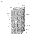
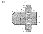
- FIG. 1 is an overall perspective view of a container 1 having an RFID module 2 according to the first embodiment of the present invention.
- FIG. 2 is a cross-sectional view taken along the line II-II in FIG. 1
- FIG. 3 is a developed view of the container 1 in FIG.
- the container 1 of the first embodiment is formed in the base material 3, the RFID module 5 attached to the base material 3, the metal film 7 formed on the first main surface 3s of the base material 3, and the metal film 7.
- the slot 9 is provided.
- the container 1 is, for example, an assembly-type box formed into a three-dimensional shape by assembling a flat base material 3 as shown in FIG.
- the container 1 has a rectangular parallelepiped shape, for example, and the base material 3 is made of, for example, paper, resin, or plastic.
- the base material 3 includes a first surface 3a, a second surface 3b, a third surface 3c, a fourth surface 3d, a fifth surface 3e, a sixth surface 3f, and a first flap 3g, a second flap 3h, and a third flap. Equipped with 3k.
- the first surface 3a to the fourth surface 3d become a side surface when assembled
- the fifth surface 3e becomes an upper surface when assembled
- the sixth surface 3f becomes a lower surface when assembled.
- the first main surface 3s of the base material 3 is a surface to be the outer surface (front surface) of the container 1
- the second main surface 3t of the base material 3 is a surface to be the inner surface (back surface) of the container 1.
- the first main surface 3s of the first flap 3g is attached to the second main surface 3t of the second surface 3b via an adhesive layer (not shown) when assembled.
- the first main surface 3s of the second flap 3h is attached to the second main surface 3t of the first surface 3a via an adhesive layer when assembled.
- the first main surface 3s of the third flap 3k is attached to the second main surface 3t of the first surface 3a via an adhesive layer when assembled.
- the metal film 7 is formed on the entire surface of the first main surface 3s of the base material 3 except for the slot 9.
- the metal film 7 is made of a film body of a conductive material of a metal foil such as an aluminum foil or a copper foil, and is formed by, for example, attaching a metal sheet. By using a metal having a small resistance value such as aluminum or copper as the metal film 7, the communication distance can be increased.
- the thickness of the metal film 7 is, for example, larger than 5 ⁇ m and 40 ⁇ m or less.
- the metal film 7 may not be formed on the entire surface of the base material 3, and may be partially formed on the third surface 3c on which the slot 9 is formed and another surface, for example.
- the communication distance becomes the maximum.
- the container 1 is irradiated with an electromagnetic wave having a communication frequency, communication is performed in a direction that orbits the slot 9 so as to reciprocate from the RFID module 5 located at the center of the longitudinal direction of the slot 9 to the ends of the two slots 9. It resonates with the frequency and the current Ir flows (see FIG. 1).
- the slot 9 is a groove formed in the region of the metal film 7.
- the width W of the slot 9 is, for example, 1 mm.
- the slot 9 may be formed by forming the metal film 7 on the entire first main surface 3s of the base material 3 and then scraping the metal film 7 with, for example, sandpaper, or two metal sheets are slotted. It may be formed by attaching it to the first main surface 3S of the base material 3 with a width of 9.
- the slot 9 is not limited to the third surface 3c of the base material 3, but may be formed on another surface.
- the RFID module 5 of the first embodiment is a wireless communication device configured to perform wireless communication (transmission / reception) with a high frequency signal having a communication frequency (carrier frequency).
- the RFID module 5 is configured to perform wireless communication with, for example, a high frequency signal having a frequency for communication in the UHF band.
- the UHF band is a frequency band from 860 MHz to 960 MHz.
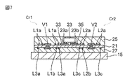
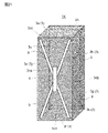
- FIG. 4 is a perspective plan view of the RFID module
- FIG. 5 is a cross-sectional view taken along the line V in FIG.
- FIG. 6 shows a plan view of a conductor pattern formed on the substrate of the RFID module
- FIG. 6a is a plan view of the conductor pattern formed on the upper surface of the substrate of the RFID module
- FIG. 6b is a plan view of the conductor pattern formed on the lower surface of the substrate. It is a perspective plan view seen from the top of the conductor pattern.
- FIG. 7 is a cross-sectional view taken along the line VII in FIG.
- the XYZ coordinate system facilitates the understanding of the invention and does not limit the invention.
- the X-axis direction indicates the longitudinal direction of the RFID module 5
- the Y-axis direction indicates the depth (width) direction
- the Z-axis direction indicates the thickness direction.
- the X, Y, and Z directions are orthogonal to each other.
- the RFID module 5 is attached to the upper surface of the metal film 7 across the slot 9 via a pressure-sensitive adhesive 15 such as double-sided tape or synthetic resin.
- the RFID module 5 includes a substrate 21 and an RFID 23 mounted on the substrate 21.
- the substrate 21 is a flexible substrate such as polyimide.
- a protective film 25 is formed on the upper surface of the substrate 21 on which the RFIC 23 is mounted.
- the protective film 25 is, for example, an elastomer such as polyurethane or a hot melt agent such as ethylene vinyl acetate (EVA).
- a protective film 27 is also attached to the lower surface of the substrate 21.
- the protective film 27 is, for example, a coverlay film such as a polyimide film (Kapton tape).
- a third electrode 33, a fourth electrode 35, a conductor pattern L1a of the main portion of the first inductance element L1 and a conductor pattern L2a of the main portion of the second inductance element L2 are formed on the upper surface of the substrate 21, a third electrode 33, a fourth electrode 35, a conductor pattern L1a of the main portion of the first inductance element L1 and a conductor pattern L2a of the main portion of the second inductance element L2 are formed.
- the third electrode 33 is connected to one end of the conductor pattern L1a
- the fourth electrode 35 is connected to one end of the conductor pattern L2a.
- These conductor patterns are, for example, a copper foil patterned by photolithography.
- the first electrode 29 and the second electrode 31 are capacitively coupled to the metal film 7, respectively. Further, on the lower surface of the substrate 21, a part of the conductor pattern L1b of the first inductance element L1 and the conductor patterns L3a, L3b (conductor pattern surrounded by the alternate long and short dash line) and L3c of the third inductance element L3 are formed. These conductor patterns are also, for example, a copper foil patterned by photolithography.
- One end of a part of the conductor pattern L1b of the first inductance element L1 and one end of the conductor pattern L3a of the third inductance element L3 are connected to the first electrode 29.
- one end of the conductor pattern L2b of the second inductance element L2 and one end of the conductor pattern L3c of the third inductance element L3 are connected to the second electrode 31.
- a conductor pattern L3b is connected between the other end of the conductor pattern L3a of the third inductance element L3 and the other end of the conductor pattern L3c.
- the other end of the conductor pattern L1b of the first inductance element L1 and the other end of the conductor pattern L1a of the first inductance element L1 are connected via the via conductor V1.
- the other end of the conductor pattern L2b of the second inductance element L2 and the other end of the conductor pattern L2a of the second inductance element L2 are connected via the via conductor V2.
- the RFIC 23 is mounted on the third electrode 33 and the fourth electrode 35 formed on the upper surface of the substrate 21. That is, the terminal 23a of the RFIC 23 is connected to the third electrode 33, and the terminal 23b of the RFIC 23 is connected to the fourth electrode 35.
- the conductor patterns L3a of the first inductance element L1 and the third inductance element L3 are formed in different layers of the substrate 21, and are arranged so that their coil openings overlap each other.
- the conductor patterns L3c of the second inductance element L2 and the third inductance element L3 are formed in different layers of the substrate 21, and the coil openings are arranged so as to overlap each other.
- the RFIC 23 is positioned on the surface of the substrate 21 between the conductor pattern L3c of the second inductance element L2 and the third inductance element L3 and the conductor pattern L3a of the first inductance element L1 and the third inductance element L3. do.
- the conductor patterns L1a, L1b, and L3a form the first coil Cr1
- the conductor patterns L2a, L2b, and L3c form the second coil Cr2.
- a first current path CP1 passing through the upper surface and the lower surface of the substrate 21 and a second current path CP2 passing through the lower surface of the substrate 21 are formed.
- the first current path CP1 reaches the second electrode 31 from the first electrode 29 through the branch point N1, the conductor pattern L1b, the conductor pattern L1a, RFIC23, the conductor pattern L2a, the conductor pattern L2b, and the branch point N2.
- the second current path CP2 reaches the second electrode 31 from the first electrode 29 through the branch point N1, the conductor pattern L3a, the conductor pattern L3b, the conductor pattern L3c, and the branch point N2.
- first inductance element L1 composed of a conductor pattern L1b connected via a conductor pattern L1a and a via conductor V1, and a conductor pattern L2b connected via a conductor pattern L2a and a via conductor V2.
- the winding directions of the current flowing through the second inductance element L2 are opposite to each other, and the magnetic field generated by the first inductance element L1 and the magnetic field generated by the second inductance element L2 cancel each other out.
- the first current path CP1 and the second current path CP2 are formed in parallel with each other between the first electrode 29 and the second electrode 31, respectively.
- the slot antenna when a slot antenna is provided in a container, the slot antenna may be affected by the contents in the container and communication may be hindered. This is because the physical length of the slot is fixed, and if the electrical length of the slot is affected by the contents such as liquid and changes, communication may not be possible. Therefore, the slot antenna is not suitable as an antenna to be formed in the container.
- the dielectric constant of the RFID tag changes and the electrical length of the slot becomes shorter than the half wavelength of the electromagnetic wave of the communication frequency.
- the change in permittivity also changes depending on the distance between the contents and the slot antenna. Therefore, each time the position of the contents changes in the box, the communication characteristics also change.
- the resonance frequency is fixed by the RFID module 5 instead of designing the frequency by the length of the slot 9, so that the slot 9 is used. It can respond to frequency changes due to length.
- the RFIC 23 is a small chip, and each coil pattern is wound so that the first coil Cr1 and the second coil Cr2 having a laminated structure cancel the magnetic field.
- the periphery of the RFID module 23 is fixed by the dielectric constant of the RFID module 5 and is not affected by the dielectric (contents) contained in the container 1, so that the frequency matching with the RFID module 23 does not change.
- the permittivity of the substrate 21 between the conductor patterns L1a and L2a and the conductor patterns L3a and L3c is fixed, and there is no change between the line capacitances.
- the conductor patterns L1a and L2a and the conductor patterns L3a and L3c are covered with a protective film 25 and a protective film 27 as a protective layer having a fixed dielectric constant, respectively. In this way, the dielectric constant of the RFID module 5 is fixed.
- a figure eight coil is formed by the first coil Cr1 and the second coil Cr2 of the RFID module 5, and the magnetic field of the RFID module 5 is formed. Is a configuration that does not easily leak to the outside. Since the magnetic field of the RFID module 5 is less likely to leak, the inductance value is less likely to change due to external factors.
- FIG. 8 is an equivalent circuit diagram of the RFID module 5.
- the first current path CP1 is a part of the parallel resonant circuit RC1 which is an LC parallel resonant circuit, and matches the radio wave of the communication frequency. Therefore, the radio wave of the communication frequency is transmitted to the metal film 7. Is received, a current flows through the RFIC 23.
- the RFID module 5 is formed with a parallel resonant circuit RC1.
- the parallel resonant circuit RC1 is a loop circuit composed of a first inductance element L1, an RFIC23, a second inductance element L2, and a third inductance element L3.
- Capacity C1 is composed of a metal film 7, a first electrode 29, an adhesive 15, and a protective film 27.
- the capacitance C2 is composed of a metal film 7, a second electrode 31, an adhesive 15, and a protective film 27.
- the fourth inductance element L4 is an inductance component of one metal film 7, and the fifth inductance element L5 is an inductance component of the other metal film 7. Since the RFID module 5 is electrically coupled to the metal film 7 forming the slot 9 via the capacitance C1 and the capacitance C2, the current flowing around the slot 9 is both the fourth inductance element L4 of the metal film 7. A current diverges and flows through the RFID module 5 through the fifth inductance element L5 of the other metal film 7 via the end of the slot 9 and through the capacitance C2.
- the parallel resonance circuit RC1 is designed to perform LC parallel resonance by impedance matching with radio waves at the communication frequency. As a result, the RFID module is matched with the RFID in the communication frequency, and the communication distance of the RFID module 5 in the communication frequency can be secured.
- the container 1 of the first embodiment is the container 1 provided with the RFID module 5, the insulating base material 3 forming the outer shape of the container 1 and the metal film 7 formed on the base material 3. And a slot 9 formed on the base material 3 in the region where the metal film 7 is formed.
- the RFID module 5 includes an RFIC 23, a parallel resonance circuit RC1 as a filter circuit for transmitting a current due to an electromagnetic wave having a unique resonance frequency which is a communication frequency to the RFIC 23, and a first electrode 29 and a second electrode connected to the parallel resonance circuit RC1. 31 and.
- the first electrode 29 of the RFID module 5 and the metal film 7 are electrically connected, and the RFID module 5 straddles the slot 9 and the second electrode 31 of the RFID module 5 and the metal film 7 are electrically connected.
- the slot 9 can be used as a slot antenna, and the current is applied to the RFID 23 by series resonance. Can be shed. Therefore, even if the container 1 is formed with the metal film 7, wireless communication is possible, and it is possible to provide the container 1 having the RFID module 5 in which the reduction in design is suppressed. Further, the container 1 of the first embodiment can be provided at a lower cost than the container to which the conventional metal-compatible RFID module is attached.
- the container 1 can obtain communication characteristics as a slot antenna.
- the length of the slot 9 has a physical length of half the wavelength of the electromagnetic wave of the communication frequency. As a result, the maximum communication distance as a slot antenna is often obtained.
- the metal film 7 is formed on the entire surface of the first main surface 3s of the base material 3 except for the slot 9. As described above, a design in which the metal film 7 is formed on the entire surface of the first main surface 3s of the container 1 can be realized.
- FIG. 9 is an overall view of the container 1A in the first modification of the first embodiment.
- the container 1A in the first modification of the first embodiment has a configuration in which the slot 9 of the container 1 of the first embodiment is formed over the second surface 3b and the third surface 3c. In this way, the slot 9 may extend over a plurality of side surfaces in a direction that orbits the container 1A in the lateral direction.
- Other configurations of the first modification of the first embodiment are substantially the same as those of the container 1 of the first embodiment.
- FIG. 9 is an overall view of the container 1B in the second modification of the first embodiment.
- FIG. 10 is a developed view of the container 1B in the second modification of the first embodiment.
- the container 1B in the second modification of the first embodiment has a configuration in which the slot 9 of the container 1 of the first embodiment is formed along the long side of the third surface 3c.
- Other configurations of the second modification of the first embodiment are substantially the same as those of the container 1 of the first embodiment.
- the container 1B in the second modification has a current Ir flowing so as to orbit along the slot 9, and supplies electric power to the RFID module 5.
- a part of the current Ir passes through the fifth surface 3e and the sixth surface 3f.
- the third surface 3c may have a recess 3v extending in the vertical direction.
- FIG. 12 is a cross-sectional view of the container 1C in the modified example 3 of the first embodiment.
- Other configurations of the third modification of the first embodiment are substantially the same as those of the container 1 of the first embodiment.
- the metal film 7 is also formed along the recess 3v, and the slot 9 is formed at the bottom of the recess 3v.
- the container 1C has a recess 3v extending in the longitudinal direction on the third surface 3c which is the side surface of the container 1C, even if a plurality of containers 1C are brought into contact with each other and arranged, the slot 9 in the recess 3v Since the metal film 7 of the other container 1c does not come into contact with the container 1, the slot 9 is not short-circuited. Therefore, it is possible to perform wireless communication with a plurality of containers 1C only by aligning the heights of the containers 1C. Further, since the concave portion 3v is formed, a gap is formed between the container 1C and the container 1C when the containers 1C are arranged, and the electromagnetic wave for communication is easily transmitted.
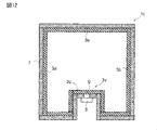
- the slot 9 may be formed at a corner between one side surface and the other side surface of the box.
- a slot 9 is formed at a corner between the second surface 3b and the third surface 3c.
- the portions of the first electrode 29 and the second electrode 31 used for the capacitive coupling at both ends of the RFID module 5 can be arranged on a plane different from the RFID 23 so as to follow the corner of the container 1D. Further, in the state where the container 1D is already attached to the metal film 7 across the cut which becomes the slot 9, since the cut is closed, the slot 9 is in a short-circuited state, so that it cannot communicate with the RFID module 5. However, when the container 1D is assembled, the slot 9 is formed so that the RFID module 5 can communicate. Therefore, it is possible to determine whether or not the assembly of the box-shaped container 1D is completed by communicating with the RFID module 5.
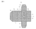
- FIG. 15 is a developed view of the container 1E in the modified example 4 of the first embodiment.
- the shape of the slot 9 is not a linear shape but a corrugated shape in the container 1 of the first embodiment. Even with such a configuration, the communication characteristics do not change, so that the container 1E of the modified example 4 of the first embodiment can obtain the same effect as the container 1 of the first embodiment.
- FIG. 16 is a developed view of the container 1F in the modified example 5 of the first embodiment.
- the shape of the slot 9 is not a linear shape but a corrugated shape in the container 1 of the first embodiment. Further, both ends of the slot 9 have a rectangular shape having a planar extension. As described above, even if the slot 9 has a combined shape of a corrugated shape and a rectangular shape, the communication characteristics do not change. Therefore, the container 1F of the modified example 5 of the first embodiment is the same as the container 1 of the first embodiment. A similar effect can be obtained.
- FIG. 17 is a developed view of the container 1G in the modified example 6 of the first embodiment.
- the container 1G in the modified example 6 of the first embodiment is inclined with respect to the long side of the third surface 3c on which the slot 9 is a side surface and extends in the vertical direction, and both ends thereof are second. It bends and extends along the short sides of the three sides and 3c. Even with such a shape of the slot 9, the communication characteristics do not change, so that the container 1G of the modification 6 of the first embodiment can obtain the same effect as the container 1 of the first embodiment.
- FIG. 18 is an overall perspective view of the container 1H in the modified example 7 of the first embodiment.
- the container 1H in the modified example 7 of the first embodiment has a tapered portion 3u having a tapered portion between the second surface 3b and the third surface 3c in the container 1 of the first embodiment, and is on the tapered portion 3u.
- This is a configuration in which the slot 9 is formed.
- a metal film 7 is continuously formed at the end of the tapered portion 3u in the width direction. Therefore, it is possible to arrange the RFID module 5 on the tapered portion 3u without bending it.
- FIG. 19 shows a cross-sectional view in which the containers 1H of the modified example 7 of the first embodiment are arranged in an overlapping manner. Since the container 1H has a slot 9 formed in the tapered portion 3u, even if a plurality of containers 1H are brought into contact with each other and arranged, the metal film 7 of the other container 1H may come into contact with the slot 9 of the tapered portion 3u. not. As a result, the slot 9 of the container 1H is not short-circuited. Therefore, it is possible to perform wireless communication with a plurality of containers 1H only by aligning the heights of the containers 1H. Further, since the tapered portion 3u is formed in the container 1H, a gap is formed between the container 1H and the container 1H when the containers 1H are arranged, and the electromagnetic wave for communication is easily transmitted.
- FIG. 20 is an overall perspective view of the container 1K in the modified example 8 of the first embodiment.
- the container 1K in the modified example 8 of the first embodiment has a configuration in which the container 1 of the first embodiment has two intersecting slots 9. Other configurations are substantially the same as the container 1 of the first embodiment.
- the RFID module 5 is arranged at the intersection of the intersecting slots 9. In this way, the degree of freedom in the design of the container 1H by the slot 9 can be improved. Further, as shown in FIGS. 20 and 21, the RFID module 5 is arranged with respect to the intersecting slots 9 so that the current flows in the lateral direction of the container 1K with respect to the RFID module 5, and flows in the vertical direction. Since it is possible to arrange the RFID module 5 in two ways, the communication characteristics of the RFID module 5 can be selected.
- the RFID module 5 has the first region 3ca and the second region 3cc as the radiation region in the third surface 3c.
- the RFID module 5 has the third region 3cc and the fourth region 3cd as the radiation region in the third surface 3c.
- FIG. 22 is a developed view of the container 1L in the modified example 9 of the first embodiment.
- the slot 9 is formed on the fifth surface 3e which is the upper surface of the container 1L of the modified example 9 of the first embodiment.
- the container 1L of the modified example 9 of the first embodiment has the same effect as the container 1 of the first embodiment. Can be obtained.
- the difference between the container 1 of the second embodiment and the container 1 of the first embodiment is the difference in the sheet resistance of the metal film 7. This difference will be mainly described below.
- the description may be omitted for the elements having the same configuration, operation, and function as those of the first embodiment, in order to avoid duplicate description.
- the container 1 of the second embodiment has the same configuration as the RFID module 5 of the first embodiment except for the points described below.
- the sheet resistance of the metal film 7 of the container 1 of the second embodiment is larger than the sheet resistance of the metal film 7 of the container 1 of the first embodiment.
- the sheet resistance of the metal film 7 is large, the following problems that did not occur in the container 1 of the first embodiment occur.
- a resonance phenomenon occurred in the entire metal film 7 around the slot 9 as an antenna electrode, and electromagnetic waves were radiated.
- the thickness of the metal film 7 in the first embodiment is, for example, larger than 5 ⁇ m and 40 ⁇ m or less, and the sheet resistance of the metal film 7 is 0.05 ⁇ / ⁇ or less.
- the metal film of the container is usually formed to prevent food oxidation and improve the design, but even if the thickness of the metal film is a single digit value in ⁇ m units such as 5 ⁇ m, the metal film is further formed.
- the printing thickness becomes about 1 ⁇ m. In this case, a step is generated in the printed matter due to the thickness of the metal film as the antenna foil, which causes printing misalignment (blurring or bleeding). For this reason, it was not possible to print directly as a design on a container with a conventional antenna foil attached.
- the sheet resistance becomes large, for example, about 0.5 ⁇ to 50 ⁇ / ⁇ .
- the resistance value of the matching circuit section between the RFIC and the antenna will be the same thickness as the metal film, the resistance value of the matching circuit section will increase, the matching loss will increase, and the RFID module will not operate.
- an antenna electrode made of a thin metal film cannot generate electromagnetic wave radiation due to the (series) resonance phenomenon, but when an electromagnetic wave is received by the metal film, a current flows through the metal film so as to cancel the electromagnetic wave. To shield.
- This current is also called an eddy current.
- an eddy current flows, the current component flowing through the metal film is not due to the resonance phenomenon of the antenna electrode, so that it can correspond to all frequency components regardless of the electrode pattern shape.
- This eddy current is known as an effect of the metal shield, but it is not usually used as an antenna.
- the RFID module 5 Since the RFID module 5 has a parallel resonant circuit RC1 as a filter circuit that transmits only a current having a unique resonance frequency to the RFID 23, the eddy current is frequency-selected and the current flows through the RFID 23 to transmit energy. Only a specific frequency is selected between the metal film 7 as an antenna electrode and the RFID module 5, impedance matching is performed, and energy transfer between the RFID 23 and the metal film 7 becomes possible. In this way, it is considered that communication with the RFIC 23 becomes possible.
- FIG. 23 is a graph showing the communication characteristics of the container 1 provided with the RFID module 5 in the second embodiment. Even in the UHF band of 830 MHz to 960 MHz, it has a communication distance of 100 cm or more, and in particular, it has a communication distance of 200 cm or more in 850 MHz to 895 MHz.
- the state where the sheet resistance of the metal film 7 is high occurs not only by the thickness of the metal film 7 but also by the manufacturing method of the metal film 7.
- the metal film 7 is formed of a conductive paste such as Ag paste
- the sheet resistance may be 0.5 ⁇ or more. Even in such a case, wireless communication can be performed if the container 1 of the second embodiment is used.
- the container 1 is an assembly type, but the present invention is not limited to this.
- the container 1 may be a bottle or a PET bottle.
- the communication frequency band is the UHF band, but the frequency band is not limited to this. It may be configured to perform wireless communication with a high frequency signal having a frequency (carrier frequency) for communication in the HF band. In this case, the total length of the metal film 7 orthogonal to the slot 9 is designed to receive a high frequency signal in the HF band.
- the HF band is a frequency band of 13 MHz or more and 15 MHz or less.
- the RFID module 5 is attached to the metal film 7, but the present invention is not limited to this.
- the RFIC 23 may be electrically connected to the metal film 7 via an inductor.
- the inductor is formed on the metal film 7 side that functions as an antenna pattern.
- the metal film 7 may have a low sheet resistance by attaching a metal foil as in the first embodiment.
- a paint may be applied on a region other than the portion where the RFID module 5 is attached to form a pattern to enhance the design of the container 1. .. Further, the metal film 7 and the slot 9 may be formed on the second main surface 3t which is the inner surface instead of the first main surface 3S which is the outer surface of the base material 3. That is, the metal film 7 and the slot 9 may be formed inside the container 1.
Abstract
Provided is a container provided with: an insulating base material forming the outer shape of the container; a metal film formed on the base material; a slot formed in the base material in the region in which the metal film is formed; and an RFID module. The RFID module is provided with: an RFIC element; a filter circuit which transmits an electric current resulting from electromagnetic waves having a unique resonant frequency, which is a communication frequency, to the RFIC element; and first and second electrodes connected to the filter circuit. The first electrode of the RFID module and the metal film are electrically connected to one another, and the second electrode of the RFID module and the metal film are electrically connected to one another with the RFID module straddling the slot.
Description
本発明は、RFIDモジュールを備えた容器、特に、誘導電磁界または電波によって、非接触でデータ通信を行うRFID(Radio Frequency Identification)技術を利用したRFIDモジュールを備えた容器に関する。
The present invention relates to a container equipped with an RFID module, particularly a container equipped with an RFID module using RFID (Radio Frequency Identification) technology for non-contact data communication by an induced electromagnetic field or radio waves.
従来、無線通信デバイスであるRFIDタグを容器に付すことで、容器内の商品の管理をすることが考えられている。RFIDタグは、RFIC(Radio-Frequency Integrated Circuit)と共に、アンテナパターンなどの金属材料が紙材や、樹脂材等の絶縁基板上に形成されている。しかしながら、容器の外面に金属膜が形成されていると、RFIDタグが影響を受けて通信ができなくなる。
Conventionally, it has been considered to manage products in a container by attaching an RFID tag, which is a wireless communication device, to the container. In RFID tags, along with RFIC (Radio-Frequency Integrated Circuit), metal materials such as antenna patterns are formed on insulating substrates such as paper materials and resin materials. However, if a metal film is formed on the outer surface of the container, the RFID tag is affected and communication becomes impossible.
上記のようなRFIDタグ付き容器において、特許文献1には、意匠性を損なわないように容器の一部に形成された金属に対応可能なRFIDタグを設けた構成が提案されている。
In the above-mentioned container with an RFID tag, Patent Document 1 proposes a configuration in which an RFID tag compatible with a metal formed in a part of the container is provided so as not to impair the design.
特許文献1に開示されたRFIDタグは、RFICチップとアンテナパターンとを有しており、これらの領域には容器に金属膜を形成することができない。したがって、より意匠性の自由度の低減を抑制したRFIDモジュールを有する容器が求められる。
The RFID tag disclosed in Patent Document 1 has an RFID chip and an antenna pattern, and a metal film cannot be formed on the container in these regions. Therefore, there is a demand for a container having an RFID module that suppresses a reduction in the degree of freedom in design.
本発明は、金属膜が形成された容器において、意匠性の低減を抑制したRFIDモジュールを有する容器の提供を目的とする。
An object of the present invention is to provide a container having an RFID module in which a reduction in design is suppressed in a container on which a metal film is formed.
本発明の一態様の容器は、RFIDモジュールを備えた容器であって、容器の外形を形成する絶縁性の基材と、基材に形成された金属膜と、金属膜が形成された領域内に基材上に形成されたスロットと、を備え、RFIDモジュールは、RFIC素子と、通信周波数である固有の共振周波数の電磁波による電流をRFIC素子に伝送するフィルタ回路と、フィルタ回路と接続する第1及び第2電極と、を備え、RFIDモジュールの第1電極と金属膜とが電気的に接続され、RFIDモジュールがスロットを跨いでRFIDモジュールの第2電極と金属膜とが電気的に接続される。
The container of one aspect of the present invention is a container provided with an RFID module, in which an insulating base material forming the outer shape of the container, a metal film formed on the base material, and a region in which the metal film is formed are formed. The RFID module is provided with a slot formed on a base material, and the RFID module is connected to the RFID element, a filter circuit that transmits a current generated by an electromagnetic wave having a unique resonance frequency, which is a communication frequency, to the RFID element, and a filter circuit. The first and second electrodes are provided, the first electrode of the RFID module and the metal film are electrically connected, the RFID module straddles the slot, and the second electrode of the RFID module and the metal film are electrically connected. To.
本発明によれば、金属膜が形成された容器において、意匠性の低減を抑制したRFIDモジュールを有する容器を提供することができる。
According to the present invention, it is possible to provide a container having an RFID module in which a reduction in design is suppressed in a container on which a metal film is formed.
本発明に係る一態様の容器は、RFIDモジュールを備えた容器であって、容器の外形を形成する絶縁性の基材と、基材に形成された金属膜と、金属膜が形成された領域内に基材上に形成されたスロットと、を備え、RFIDモジュールは、RFIC素子と、通信周波数である固有の共振周波数の電磁波による電流をRFIC素子に伝送するフィルタ回路と、フィルタ回路と接続する第1及び第2電極と、を備え、RFIDモジュールの第1電極と金属膜とが電気的に接続され、RFIDモジュールがスロットを跨いでRFIDモジュールの第2電極と金属膜とが電気的に接続される。
The container of one aspect according to the present invention is a container provided with an RFID module, and has an insulating base material forming the outer shape of the container, a metal film formed on the base material, and a region where the metal film is formed. The RFID module is provided with a slot formed on a substrate inside, and the RFID module is connected to the RFID element, a filter circuit that transmits a current generated by an electromagnetic wave having a unique resonance frequency, which is a communication frequency, to the RFID element, and a filter circuit. The first and second electrodes are provided, the first electrode of the RFID module and the metal film are electrically connected, the RFID module straddles the slot, and the second electrode of the RFID module and the metal film are electrically connected. Will be done.
この態様の容器は、容器の基材に形成された金属膜をアンテナとして利用するので、金属膜が形成された容器において、意匠性の自由度の低減を抑制してRFIDモジュールを容器に取り付けることができる。
Since the container of this embodiment uses the metal film formed on the base material of the container as an antenna, the RFID module is attached to the container in which the metal film is formed while suppressing the reduction in the degree of freedom in design. Can be done.
また、通信周波数の電磁波が金属膜に照射されると、スロットを周回する方向に電流が流れてもよい。このように、金属膜はスロットアンテナとして機能するので、スロットアンテナとしての通信特性を得ることができる。
Further, when the metal film is irradiated with an electromagnetic wave having a communication frequency, a current may flow in the direction of orbiting the slot. As described above, since the metal film functions as a slot antenna, communication characteristics as a slot antenna can be obtained.
スロットの長さは、通信周波数の電磁波の2分の1波長の物理的長さを有してもよい。この場合、スロットアンテナとしての最大の通信距離を得ることが多い。
The length of the slot may have a physical length of half the wavelength of the electromagnetic wave of the communication frequency. In this case, the maximum communication distance as a slot antenna is often obtained.
RFIDモジュールを備えた容器は、組み立て式の箱でもよい。
The container equipped with the RFID module may be a prefabricated box.
箱の側面に側面の長手方向に延びる凹部を有し、凹部にスロットが形成されてもよい。これにより、複数の容器を同じ向きで配列しても、スロットと金属膜とが接触するのを防止し、他の容器の金属膜によりスロットが短絡してRFIDモジュールを経由しないで導通することがない。したがって、複数の容器と一度に通信することができる。また、凹部が形成されていることで、容器を配列した際に容器と容器との間に隙間が形成され、通信用の電磁波が伝わりやすくなる。
The side surface of the box may have a recess extending in the longitudinal direction of the side surface, and a slot may be formed in the recess. This prevents the slot from coming into contact with the metal film even if multiple containers are arranged in the same orientation, and the metal film of the other container causes the slot to short-circuit and conduct without passing through the RFID module. not. Therefore, it is possible to communicate with a plurality of containers at once. Further, since the concave portion is formed, a gap is formed between the containers when the containers are arranged, and electromagnetic waves for communication are easily transmitted.
The side surface of the box may have a recess extending in the longitudinal direction of the side surface, and a slot may be formed in the recess. This prevents the slot from coming into contact with the metal film even if multiple containers are arranged in the same orientation, and the metal film of the other container causes the slot to short-circuit and conduct without passing through the RFID module. not. Therefore, it is possible to communicate with a plurality of containers at once. Further, since the concave portion is formed, a gap is formed between the containers when the containers are arranged, and electromagnetic waves for communication are easily transmitted.
箱の第1側面と第2側面との間の角にスロットが形成されてもよい。
Slots may be formed at the corners between the first and second sides of the box.
スロットは、箱の第1側面と第2側面との間に形成されたテーパー部に形成されてもよい。これにより、複数の容器を同じ向きで配列しても、スロットと金属膜とが接触するのを防止し、他の容器の金属膜によりスロットが短絡してRFIDモジュールを経由しないで導通することがない。したがって、複数の容器と一度に通信することができる。また、テーパー部が形成されていることで、容器を配列した際に容器と容器との間に隙間が形成され、通信用の電磁波が伝わりやすくなる。
The slot may be formed in a tapered portion formed between the first side surface and the second side surface of the box. This prevents the slot from coming into contact with the metal film even if multiple containers are arranged in the same orientation, and the metal film of the other container causes the slot to short-circuit and conduct without passing through the RFID module. not. Therefore, it is possible to communicate with a plurality of containers at once. Further, since the tapered portion is formed, a gap is formed between the containers when the containers are arranged, and electromagnetic waves for communication are easily transmitted.
金属膜は、スロットを除いて基材の全面に形成されてもよい。容器の外面の全面に金属膜を形成する意匠も実現可能である。
The metal film may be formed on the entire surface of the base material except for the slots. It is also possible to realize a design in which a metal film is formed on the entire outer surface of the container.
フィルタ回路は、LC並列共振回路でもよい。これにより、RFICとマッチングする周波数の電流をRFICに流すことができる。
The filter circuit may be an LC parallel resonant circuit. As a result, a current having a frequency matching the RFIC can be passed through the RFIC.
フィルタ回路は、基板上に形成されたコイルを有し、コイルは、保護層で覆われてもよい。これにより、コイルの誘電率を固定することができ、容器内の誘電体の影響を受けるのを防止することができる。
The filter circuit has a coil formed on the substrate, and the coil may be covered with a protective layer. As a result, the dielectric constant of the coil can be fixed, and it is possible to prevent the influence of the dielectric material in the container.
フィルタ回路のコイルは、8の字形状を有してもよい。これにより、コイルの磁界が外部に漏れにくくすることができ、コイルのインダクタンス値を外部要因で変化しにくくすることができる。
The coil of the filter circuit may have a figure eight shape. As a result, the magnetic field of the coil can be made difficult to leak to the outside, and the inductance value of the coil can be made difficult to change due to an external factor.
金属膜のシート抵抗は0.5Ω/□以上でもよい。この構成であっても、RFIDモジュールがフィルタ回路を有するので、金属膜に発生した渦電流を利用してRFICに流すことができる。
The sheet resistance of the metal film may be 0.5Ω / □ or more. Even with this configuration, since the RFID module has a filter circuit, the eddy current generated in the metal film can be used to flow through the RFID.
金属膜の厚みは1nm以上1μm以下であってもよい。この構成であっても、RFIDモジュールがフィルタ回路を有するので、金属膜に発生した渦電流を利用してRFICに流すことができる。
The thickness of the metal film may be 1 nm or more and 1 μm or less. Even with this configuration, since the RFID module has a filter circuit, the eddy current generated in the metal film can be used to flow through the RFID.
なお、以下で説明する実施の形態は、いずれも本発明の一具体例を示すものであり、本発明がこの構成に限定されるものではない。また、以下の実施の形態において具体的に示される数値、形状、構成、ステップ、ステップの順序などは、一例を示すものであり、本発明を限定するものではない。以下の実施の形態における構成要素のうち、最上位概念を示す独立請求項に記載されていない構成要素については、任意の構成要素として説明される。また、全ての実施の形態において、各変形例における構成も同様であり、各変形例に記載した構成をそれぞれ組み合わせてもよい。
Note that all of the embodiments described below show a specific example of the present invention, and the present invention is not limited to this configuration. Further, the numerical values, shapes, configurations, steps, the order of steps, etc. specifically shown in the following embodiments are only examples, and do not limit the present invention. Among the components in the following embodiments, the components not described in the independent claim indicating the highest level concept are described as arbitrary components. Further, in all the embodiments, the configuration in each modification is the same, and the configurations described in each modification may be combined.
なお、比誘電率εr>1の場合、アンテナパターン及び導体パターンの電気的長さは物理的長さに対して長くなる。本明細書において、電気的長さとは、比誘電率や寄生リアクタンス成分による波長の短縮や延長を考慮した長さである。
When the relative permittivity εr> 1, the electrical length of the antenna pattern and the conductor pattern is longer than the physical length. In the present specification, the electrical length is a length considering the shortening or extension of the wavelength due to the relative permittivity and the parasitic reactance component.
(実施形態1)
次に、本発明に係るRFIDモジュール5を備える容器1の概略構成について説明する。図1は、本発明に係る実施形態1のRFIDモジュール2を有する容器1の全体斜視図である。図2は、図1におけるII-II矢視断面図であり、図3は図1における容器1の展開図である。 (Embodiment 1)
Next, a schematic configuration of thecontainer 1 provided with the RFID module 5 according to the present invention will be described. FIG. 1 is an overall perspective view of a container 1 having an RFID module 2 according to the first embodiment of the present invention. FIG. 2 is a cross-sectional view taken along the line II-II in FIG. 1, and FIG. 3 is a developed view of the container 1 in FIG.
次に、本発明に係るRFIDモジュール5を備える容器1の概略構成について説明する。図1は、本発明に係る実施形態1のRFIDモジュール2を有する容器1の全体斜視図である。図2は、図1におけるII-II矢視断面図であり、図3は図1における容器1の展開図である。 (Embodiment 1)
Next, a schematic configuration of the
実施形態1の容器1は、基材3と、基材3に貼り付けられたRFIDモジュール5と、基材3の第1主面3sに形成された金属膜7と、金属膜7内に形成されたスロット9とを備える。
The container 1 of the first embodiment is formed in the base material 3, the RFID module 5 attached to the base material 3, the metal film 7 formed on the first main surface 3s of the base material 3, and the metal film 7. The slot 9 is provided.
容器1は、例えば、図3に示すような平面状の基材3を組み立てることで立体形状に形成される組み立て式の箱である。容器1は、例えば、直方体形状であり、基材3は、例えば、紙製、樹脂製、またはプラスチック製である。
The container 1 is, for example, an assembly-type box formed into a three-dimensional shape by assembling a flat base material 3 as shown in FIG. The container 1 has a rectangular parallelepiped shape, for example, and the base material 3 is made of, for example, paper, resin, or plastic.
基材3は、第1面3a、第2面3b、第3面3c、第4面3d、第5面3e、第6面3f、及び、第1フラップ3g、第2フラップ3h、第3フラップ3kを備える。例えば、第1面3a~第4面3dは組み立てた際に側面となり、第5面3eは組み立てた際に上面となり、第6面3fは組み立てた際に下面となる。基材3の第1主面3sは容器1の外面(表面)となる面であり、基材3の第2主面3tは容器1の内面(裏面)となる面である。
The base material 3 includes a first surface 3a, a second surface 3b, a third surface 3c, a fourth surface 3d, a fifth surface 3e, a sixth surface 3f, and a first flap 3g, a second flap 3h, and a third flap. Equipped with 3k. For example, the first surface 3a to the fourth surface 3d become a side surface when assembled, the fifth surface 3e becomes an upper surface when assembled, and the sixth surface 3f becomes a lower surface when assembled. The first main surface 3s of the base material 3 is a surface to be the outer surface (front surface) of the container 1, and the second main surface 3t of the base material 3 is a surface to be the inner surface (back surface) of the container 1.
第1フラップ3gの第1主面3sは組み立てた際に第2面3bの第2主面3tに接着層(図示省略)を介して貼り付けられる。第2フラップ3hの第1主面3sは組み立てた際に第1面3aの第2主面3tに接着層を介して貼り付けられる。第3フラップ3kの第1主面3sは組み立てた際に第1面3aの第2主面3tに接着層を介して貼り付けられる。
The first main surface 3s of the first flap 3g is attached to the second main surface 3t of the second surface 3b via an adhesive layer (not shown) when assembled. The first main surface 3s of the second flap 3h is attached to the second main surface 3t of the first surface 3a via an adhesive layer when assembled. The first main surface 3s of the third flap 3k is attached to the second main surface 3t of the first surface 3a via an adhesive layer when assembled.
金属膜7は、スロット9を除いて基材3の第1主面3sの全面に形成されている。金属膜7は、アルミニウム箔や銅箔などの金属箔の導電材料の膜体により作製され、例えば、金属シートを貼り付けることで形成される。金属膜7として、アルミニウムや銅などの抵抗値の小さい金属を用いることで通信距離を遠くすることができる。金属膜7の厚みは、例えば、5μmよりも大きく40μm以下である。なお、金属膜7は基材3の全面に形成されていなくてもよく、例えば、スロット9が形成されている第3面3cと他の面において部分的に形成されていてもよい。
The metal film 7 is formed on the entire surface of the first main surface 3s of the base material 3 except for the slot 9. The metal film 7 is made of a film body of a conductive material of a metal foil such as an aluminum foil or a copper foil, and is formed by, for example, attaching a metal sheet. By using a metal having a small resistance value such as aluminum or copper as the metal film 7, the communication distance can be increased. The thickness of the metal film 7 is, for example, larger than 5 μm and 40 μm or less. The metal film 7 may not be formed on the entire surface of the base material 3, and may be partially formed on the third surface 3c on which the slot 9 is formed and another surface, for example.
スロット9の長さLgが通信周波数の電磁波の半波長の長さである場合、通信距離が最大となる。通信周波数の電磁波が容器1に照射されると、スロット9の長手方向の中心部に位置するRFIDモジュール5から2つのスロット9の端部までをそれぞれ往復するようにスロット9を周回する方向に通信周波数と共振し電流Irが流れる(図1参照)。
When the length Lg of the slot 9 is the length of the half wavelength of the electromagnetic wave of the communication frequency, the communication distance becomes the maximum. When the container 1 is irradiated with an electromagnetic wave having a communication frequency, communication is performed in a direction that orbits the slot 9 so as to reciprocate from the RFID module 5 located at the center of the longitudinal direction of the slot 9 to the ends of the two slots 9. It resonates with the frequency and the current Ir flows (see FIG. 1).
スロット9は、金属膜7の領域内に形成された溝である。スロット9の幅Wは、例えば、1mmである。スロット9は、基材3の第1主面3s全体に金属膜7を形成した後に金属膜7を、例えば、サンドペーパー等で削ることで形成してもよいし、2枚の金属シートをスロット9の幅を空けて基材3の第1主面3Sに貼り付けることで形成してもよい。なお、スロット9は、基材3の第3面3c上に限らず他の面に形成されてもよい。
The slot 9 is a groove formed in the region of the metal film 7. The width W of the slot 9 is, for example, 1 mm. The slot 9 may be formed by forming the metal film 7 on the entire first main surface 3s of the base material 3 and then scraping the metal film 7 with, for example, sandpaper, or two metal sheets are slotted. It may be formed by attaching it to the first main surface 3S of the base material 3 with a width of 9. The slot 9 is not limited to the third surface 3c of the base material 3, but may be formed on another surface.
実施形態1のRFIDモジュール5は、通信周波数(キャリア周波数)を有する高周波信号で無線通信(送受信)するように構成された無線通信デバイスである。RFIDモジュール5は、例えば、UHF帯の通信用の周波数を有する高周波信号で無線通信するよう構成されている。ここでUHF帯とは、860MHzから960MHzの周波数帯域である。
The RFID module 5 of the first embodiment is a wireless communication device configured to perform wireless communication (transmission / reception) with a high frequency signal having a communication frequency (carrier frequency). The RFID module 5 is configured to perform wireless communication with, for example, a high frequency signal having a frequency for communication in the UHF band. Here, the UHF band is a frequency band from 860 MHz to 960 MHz.
次に、図4から図7を参照して、RFIDモジュール5の構成について説明する。図4は、RFIDモジュールの透視平面図であり、図5は、図4における矢視Vの断面図である。図6はRFIDモジュールの基板に形成されている導体パターンの平面図を示し、図6aはRFIDモジュールの基板の上面に形成された導体パターンの平面図であり、図6bは基板の下面に形成された導体パターンの上から見た透視平面図である。図7は、図4における矢視VIIの断面図である。図中において、X-Y-Z座標系は、発明の理解を容易にするものであって、発明を限定するものではない。X軸方向はRFIDモジュール5の長手方向を示し、Y軸方向は奥行き(幅)方向を示し、Z軸方向は厚さ方向を示している。X、Y、Z方向は互いに直交する。
Next, the configuration of the RFID module 5 will be described with reference to FIGS. 4 to 7. FIG. 4 is a perspective plan view of the RFID module, and FIG. 5 is a cross-sectional view taken along the line V in FIG. FIG. 6 shows a plan view of a conductor pattern formed on the substrate of the RFID module, FIG. 6a is a plan view of the conductor pattern formed on the upper surface of the substrate of the RFID module, and FIG. 6b is a plan view of the conductor pattern formed on the lower surface of the substrate. It is a perspective plan view seen from the top of the conductor pattern. FIG. 7 is a cross-sectional view taken along the line VII in FIG. In the figure, the XYZ coordinate system facilitates the understanding of the invention and does not limit the invention. The X-axis direction indicates the longitudinal direction of the RFID module 5, the Y-axis direction indicates the depth (width) direction, and the Z-axis direction indicates the thickness direction. The X, Y, and Z directions are orthogonal to each other.
図4に示すように、RFIDモジュール5は、両面テープまたは合成樹脂等の粘着剤15を介して金属膜7の上面にスロット9を跨いで貼り合わされる。
As shown in FIG. 4, the RFID module 5 is attached to the upper surface of the metal film 7 across the slot 9 via a pressure-sensitive adhesive 15 such as double-sided tape or synthetic resin.
図5に示すように、RFIDモジュール5は、基板21と、基板21に搭載されるRFIC23とを備える。基板21は、例えば、ポリイミド等のフレキシブル基板である。RFIC23が実装された基板21の上面には保護膜25が形成されている。保護膜25は、例えば、ポリウレタン等のエラストマや、エチレン酢酸ビニル(EVA)のようなホットメルト剤である。基板21の下面にも、保護フィルム27が貼り付けられている。保護フィルム27は、例えば、ポリイミドフィルム(カプトンテープ)等のカバーレイフィルムである。
As shown in FIG. 5, the RFID module 5 includes a substrate 21 and an RFID 23 mounted on the substrate 21. The substrate 21 is a flexible substrate such as polyimide. A protective film 25 is formed on the upper surface of the substrate 21 on which the RFIC 23 is mounted. The protective film 25 is, for example, an elastomer such as polyurethane or a hot melt agent such as ethylene vinyl acetate (EVA). A protective film 27 is also attached to the lower surface of the substrate 21. The protective film 27 is, for example, a coverlay film such as a polyimide film (Kapton tape).
図6を参照する。基板21の上面には、第3電極33、第4電極35、第1インダクタンス素子L1の主要部の導体パターンL1a、および、第2インダクタンス素子L2の主要部の導体パターンL2aが形成されている。第3電極33は導体パターンL1aの一端と接続され、第4電極35は導体パターンL2aの一端と接続されている。これらの導体パターンは、例えば、銅箔をフォトリソグラフィによってパターニングしたものである。
Refer to FIG. On the upper surface of the substrate 21, a third electrode 33, a fourth electrode 35, a conductor pattern L1a of the main portion of the first inductance element L1 and a conductor pattern L2a of the main portion of the second inductance element L2 are formed. The third electrode 33 is connected to one end of the conductor pattern L1a, and the fourth electrode 35 is connected to one end of the conductor pattern L2a. These conductor patterns are, for example, a copper foil patterned by photolithography.
基板21の下面には、金属膜7にそれぞれ容量結合される第1電極29および第2電極31が形成されている。また、基板21の下面には、第1インダクタンス素子L1の一部の導体パターンL1b、第3インダクタンス素子L3の導体パターンL3a、L3b(二点鎖線で囲む導体パターン)、L3cが形成されている。これらの導体パターンも、例えば、銅箔をフォトリソグラフィによってパターニングしたものである。
On the lower surface of the substrate 21, the first electrode 29 and the second electrode 31 are capacitively coupled to the metal film 7, respectively. Further, on the lower surface of the substrate 21, a part of the conductor pattern L1b of the first inductance element L1 and the conductor patterns L3a, L3b (conductor pattern surrounded by the alternate long and short dash line) and L3c of the third inductance element L3 are formed. These conductor patterns are also, for example, a copper foil patterned by photolithography.
第1インダクタンス素子L1の一部の導体パターンL1bの一端と第3インダクタンス素子L3の導体パターンL3aの一端とが第1電極29と接続されている。同様に、第2インダクタンス素子L2の導体パターンL2bの一端と第3インダクタンス素子L3の導体パターンL3cの一端とが第2電極31と接続されている。第3インダクタンス素子L3の導体パターンL3aの他端と、導体パターンL3cの他端との間には、導体パターンL3bが接続されている。
One end of a part of the conductor pattern L1b of the first inductance element L1 and one end of the conductor pattern L3a of the third inductance element L3 are connected to the first electrode 29. Similarly, one end of the conductor pattern L2b of the second inductance element L2 and one end of the conductor pattern L3c of the third inductance element L3 are connected to the second electrode 31. A conductor pattern L3b is connected between the other end of the conductor pattern L3a of the third inductance element L3 and the other end of the conductor pattern L3c.
第1インダクタンス素子L1の導体パターンL1bの他端と、第1インダクタンス素子L1の導体パターンL1aの他端とは、ビア導体V1を介して接続されている。同様に、第2インダクタンス素子L2の導体パターンL2bの他端と、第2インダクタンス素子L2の導体パターンL2aの他端とは、ビア導体V2を介して接続されている。
The other end of the conductor pattern L1b of the first inductance element L1 and the other end of the conductor pattern L1a of the first inductance element L1 are connected via the via conductor V1. Similarly, the other end of the conductor pattern L2b of the second inductance element L2 and the other end of the conductor pattern L2a of the second inductance element L2 are connected via the via conductor V2.
基板21の上面に形成された第3電極33および第4電極35にRFIC23が搭載されている。つまり、RFIC23の端子23aが第3電極33に接続されて、RFIC23の端子23bが第4電極35に接続されている。
The RFIC 23 is mounted on the third electrode 33 and the fourth electrode 35 formed on the upper surface of the substrate 21. That is, the terminal 23a of the RFIC 23 is connected to the third electrode 33, and the terminal 23b of the RFIC 23 is connected to the fourth electrode 35.
第1インダクタンス素子L1と第3インダクタンス素子L3の導体パターンL3aとは、基板21の異なる層にそれぞれ形成され、かつ、それぞれのコイル開口が重なる関係に配置されている。同様に、第2インダクタンス素子L2および第3インダクタンス素子L3の導体パターンL3cとは、基板21の異なる層にそれぞれ形成され、かつ、それぞれのコイル開口が重なる関係に配置されている。さらに、RFIC23は、基板21の面上で、第2インダクタンス素子L2および第3インダクタンス素子L3の導体パターンL3cと、第1インダクタンス素子L1および第3インダクタンス素子L3の導体パターンL3aとの間に、位置する。導体パターンL1a、L1b、及びL3aで第1コイルCr1を構成し、導体パターンL2a、L2b、及びL3cで第2コイルCr2を構成する。
The conductor patterns L3a of the first inductance element L1 and the third inductance element L3 are formed in different layers of the substrate 21, and are arranged so that their coil openings overlap each other. Similarly, the conductor patterns L3c of the second inductance element L2 and the third inductance element L3 are formed in different layers of the substrate 21, and the coil openings are arranged so as to overlap each other. Further, the RFIC 23 is positioned on the surface of the substrate 21 between the conductor pattern L3c of the second inductance element L2 and the third inductance element L3 and the conductor pattern L3a of the first inductance element L1 and the third inductance element L3. do. The conductor patterns L1a, L1b, and L3a form the first coil Cr1, and the conductor patterns L2a, L2b, and L3c form the second coil Cr2.
RFIDモジュール5内において、基板21の上面及び下面を通る第1電流経路CP1と基板21の下面を通る第2電流経路CP2とが形成されている。第1電流経路CP1は、第1電極29から分岐点N1、導体パターンL1b、導体パターンL1a、RFIC23、導体パターンL2a、導体パターンL2b、分岐点N2、を通って第2電極31に至る。第2電流経路CP2は、第1電極29から分岐点N1、導体パターンL3a、導体パターンL3b、導体パターンL3c、分岐点N2を通って第2電極31に至る。ここで、導体パターンL1aとビア導体V1を介して接続している導体パターンL1bで構成される第1インダクタンス素子L1と、導体パターンL2aとビア導体V2を介して接続している導体パターンL2bで構成される第2インダクタンス素子L2に流れる電流の巻き方向は逆になっており、第1インダクタンス素子L1で発生する磁界と第2インダクタンス素子L2で発生する磁界はお互いに打ち消し合っている。第1電流経路CP1及び第2電流経路CP2は、それぞれ、第1電極29と第2電極31との間で、互いに並列に形成されている。
In the RFID module 5, a first current path CP1 passing through the upper surface and the lower surface of the substrate 21 and a second current path CP2 passing through the lower surface of the substrate 21 are formed. The first current path CP1 reaches the second electrode 31 from the first electrode 29 through the branch point N1, the conductor pattern L1b, the conductor pattern L1a, RFIC23, the conductor pattern L2a, the conductor pattern L2b, and the branch point N2. The second current path CP2 reaches the second electrode 31 from the first electrode 29 through the branch point N1, the conductor pattern L3a, the conductor pattern L3b, the conductor pattern L3c, and the branch point N2. Here, it is composed of a first inductance element L1 composed of a conductor pattern L1b connected via a conductor pattern L1a and a via conductor V1, and a conductor pattern L2b connected via a conductor pattern L2a and a via conductor V2. The winding directions of the current flowing through the second inductance element L2 are opposite to each other, and the magnetic field generated by the first inductance element L1 and the magnetic field generated by the second inductance element L2 cancel each other out. The first current path CP1 and the second current path CP2 are formed in parallel with each other between the first electrode 29 and the second electrode 31, respectively.
従来、容器にスロットアンテナを設けた場合、スロットアンテナが容器内の内容物により影響を受けて通信が妨げられる場合があった。これは、スロットの物理的長さが固定されており、液体等の内容物によってスロットの電気的長さが影響を受けて変化すると、通信ができなくなる場合がある。したがって、容器に形成するアンテナとしてスロットアンテナは不向きであった。
Conventionally, when a slot antenna is provided in a container, the slot antenna may be affected by the contents in the container and communication may be hindered. This is because the physical length of the slot is fixed, and if the electrical length of the slot is affected by the contents such as liquid and changes, communication may not be possible. Therefore, the slot antenna is not suitable as an antenna to be formed in the container.
液体等の誘電体を容器内に収容する場合、RFIDタグの誘電率が変化してスロットの電気長が通信周波数の電磁波の半波長よりも短くなる。また、誘電率の変化は内容物とスロットアンテナとの距離によっても変化する。したがって、内容物の位置が箱の中で変わるごとに通信特性も変化する。
When a dielectric such as a liquid is stored in a container, the dielectric constant of the RFID tag changes and the electrical length of the slot becomes shorter than the half wavelength of the electromagnetic wave of the communication frequency. The change in permittivity also changes depending on the distance between the contents and the slot antenna. Therefore, each time the position of the contents changes in the box, the communication characteristics also change.
実施形態1において、この誘電率の変化による波長変化(周波数変化)を避けるために、スロット9の長さで周波数設計するのではなく、RFIDモジュール5で共振周波数を固定することで、スロット9の長さによる周波数変化に対応できる。
In the first embodiment, in order to avoid the wavelength change (frequency change) due to the change in the permittivity, the resonance frequency is fixed by the RFID module 5 instead of designing the frequency by the length of the slot 9, so that the slot 9 is used. It can respond to frequency changes due to length.
また、RFIC23は小型のチップであり、積層構造した第1コイルCr1及び第2コイルCr2が磁界を打ち消すようにそれぞれのコイルパターンが巻かれている。これにより、RFIC23の周辺はRFIDモジュール5の誘電率で固定され、容器1に収容される誘電体(内容物)による影響を受けないので、RFIC23にマッチングする周波数が変化しない。図7を参照すると、導体パターンL1a、L2aと、導体パターンL3a、L3c間の基板21の誘電率が固定しており、線間容量間の変化がない。また、導体パターンL1a、L2aと、導体パターンL3a、L3cとは、固定の誘電率の保護層としての保護膜25及び保護フィルム27でそれぞれ覆われている。このようにして、RFIDモジュール5の誘電率が固定されている。
Further, the RFIC 23 is a small chip, and each coil pattern is wound so that the first coil Cr1 and the second coil Cr2 having a laminated structure cancel the magnetic field. As a result, the periphery of the RFID module 23 is fixed by the dielectric constant of the RFID module 5 and is not affected by the dielectric (contents) contained in the container 1, so that the frequency matching with the RFID module 23 does not change. Referring to FIG. 7, the permittivity of the substrate 21 between the conductor patterns L1a and L2a and the conductor patterns L3a and L3c is fixed, and there is no change between the line capacitances. Further, the conductor patterns L1a and L2a and the conductor patterns L3a and L3c are covered with a protective film 25 and a protective film 27 as a protective layer having a fixed dielectric constant, respectively. In this way, the dielectric constant of the RFID module 5 is fixed.
また、容器1内の誘電体の誘電率の影響を小さくするために、RFIDモジュール5の第1コイルCr1と、第2コイルCr2とで8の字コイルを形成しており、RFIDモジュール5の磁界が外部に漏れにくい構成である。RFIDモジュール5の磁界が漏れにくいのでインダクタンス値が外部要因で変化しにくい構成である。
Further, in order to reduce the influence of the dielectric constant of the dielectric in the container 1, a figure eight coil is formed by the first coil Cr1 and the second coil Cr2 of the RFID module 5, and the magnetic field of the RFID module 5 is formed. Is a configuration that does not easily leak to the outside. Since the magnetic field of the RFID module 5 is less likely to leak, the inductance value is less likely to change due to external factors.
また、RFIDモジュール5の磁束も閉じているので、容器1の中に金属を収容する場合でも、RFIC23にマッチングする周波数の変化が小さくなる。
Further, since the magnetic flux of the RFID module 5 is also closed, the change in the frequency matching with the RFID 23 is small even when the metal is housed in the container 1.
次に、図8を参照して、RFIDモジュール5の回路構成について説明する。図8はRFIDモジュール5の等価回路図である。
Next, the circuit configuration of the RFID module 5 will be described with reference to FIG. FIG. 8 is an equivalent circuit diagram of the RFID module 5.
RFIDモジュール5内において、第1電流経路CP1は、LC並列共振回路である並列共振回路RC1の一部であり、通信周波数の電波に対してマッチングしているので、通信周波数の電波を金属膜7が受信すると、RFIC23に電流が流れる。
In the RFID module 5, the first current path CP1 is a part of the parallel resonant circuit RC1 which is an LC parallel resonant circuit, and matches the radio wave of the communication frequency. Therefore, the radio wave of the communication frequency is transmitted to the metal film 7. Is received, a current flows through the RFIC 23.
RFIDモジュール5は、並列共振回路RC1が形成されている。並列共振回路RC1は、第1インダクタンス素子L1、RFIC23、第2インダクタンス素子L2、および、第3インダクタンス素子L3で構成されるループ回路である。
The RFID module 5 is formed with a parallel resonant circuit RC1. The parallel resonant circuit RC1 is a loop circuit composed of a first inductance element L1, an RFIC23, a second inductance element L2, and a third inductance element L3.
容量C1は、金属膜7、第1電極29、粘着剤15、および保護フィルム27で構成される。容量C2は、金属膜7、第2電極31、粘着剤15、および保護フィルム27で構成される。第4インダクタンス素子L4は一方の金属膜7のインダクタンス成分であり、第5インダクタンス素子L5は他方の金属膜7のインダクタンス成分である。RFIDモジュール5はスロット9を形成する金属膜7と容量C1及び容量C2を介して電気的に結合しているので、スロット9の周囲に流れる電流は、金属膜7の第4インダクタンス素子L4の両方に電流が分岐して流れ、スロット9端部を介して他方の金属膜7の第5インダクタンス素子L5を通り容量C2を介して、RFIDモジュール5に流れ込んでいる。
Capacity C1 is composed of a metal film 7, a first electrode 29, an adhesive 15, and a protective film 27. The capacitance C2 is composed of a metal film 7, a second electrode 31, an adhesive 15, and a protective film 27. The fourth inductance element L4 is an inductance component of one metal film 7, and the fifth inductance element L5 is an inductance component of the other metal film 7. Since the RFID module 5 is electrically coupled to the metal film 7 forming the slot 9 via the capacitance C1 and the capacitance C2, the current flowing around the slot 9 is both the fourth inductance element L4 of the metal film 7. A current diverges and flows through the RFID module 5 through the fifth inductance element L5 of the other metal film 7 via the end of the slot 9 and through the capacitance C2.
並列共振回路RC1は、通信周波数における電波に対してインピーダンス整合してLC並列共振するように設計されている。これにより、通信周波数でRFICとマッチングしており、通信周波数におけるRFIDモジュール5の通信距離を確保することができる。
The parallel resonance circuit RC1 is designed to perform LC parallel resonance by impedance matching with radio waves at the communication frequency. As a result, the RFID module is matched with the RFID in the communication frequency, and the communication distance of the RFID module 5 in the communication frequency can be secured.
以上のように、実施形態1の容器1は、RFIDモジュール5を備えた容器1であって、容器1の外形を形成する絶縁性の基材3と、基材3に形成された金属膜7と、金属膜7が形成された領域内に基材3上に形成されたスロット9と、を備える。RFIDモジュール5は、RFIC23と、通信周波数である固有の共振周波数の電磁波による電流をRFIC23に伝送するフィルタ回路としての並列共振回路RC1と、並列共振回路RC1と接続する第1電極29及び第2電極31と、を備える。RFIDモジュール5の第1電極29と金属膜7とが電気的に接続され、RFIDモジュール5がスロット9を跨いでRFIDモジュール5の第2電極31と金属膜7とが電気的に接続される。
As described above, the container 1 of the first embodiment is the container 1 provided with the RFID module 5, the insulating base material 3 forming the outer shape of the container 1 and the metal film 7 formed on the base material 3. And a slot 9 formed on the base material 3 in the region where the metal film 7 is formed. The RFID module 5 includes an RFIC 23, a parallel resonance circuit RC1 as a filter circuit for transmitting a current due to an electromagnetic wave having a unique resonance frequency which is a communication frequency to the RFIC 23, and a first electrode 29 and a second electrode connected to the parallel resonance circuit RC1. 31 and. The first electrode 29 of the RFID module 5 and the metal film 7 are electrically connected, and the RFID module 5 straddles the slot 9 and the second electrode 31 of the RFID module 5 and the metal film 7 are electrically connected.
容器1の基材3に形成された金属膜7に形成されたスロット9を跨いでRFIDモジュール5が配置されているので、スロット9をスロットアンテナとして利用することができ、直列共振によりRFIC23に電流を流すことができる。したがって、金属膜7が形成された容器1であっても、無線通信が可能であり、意匠性の低減を抑制したRFIDモジュール5を有する容器1を提供することができる。また、実施形態1の容器1であれば、従来の金属対応のRFIDモジュールを取り付けた容器よりも安価に提供することができる。
Since the RFID module 5 is arranged across the slot 9 formed in the metal film 7 formed on the base material 3 of the container 1, the slot 9 can be used as a slot antenna, and the current is applied to the RFID 23 by series resonance. Can be shed. Therefore, even if the container 1 is formed with the metal film 7, wireless communication is possible, and it is possible to provide the container 1 having the RFID module 5 in which the reduction in design is suppressed. Further, the container 1 of the first embodiment can be provided at a lower cost than the container to which the conventional metal-compatible RFID module is attached.
通信周波数の電磁波が金属膜7に照射されると、スロット9を周回する方向に電流が流れる。このように、スロット9の周囲の金属膜7はスロットアンテナとして機能するので、容器1はスロットアンテナとしての通信特性を得ることができる。
When the metal film 7 is irradiated with an electromagnetic wave having a communication frequency, a current flows in the direction around the slot 9. As described above, since the metal film 7 around the slot 9 functions as a slot antenna, the container 1 can obtain communication characteristics as a slot antenna.
また、スロット9の長さは、通信周波数の電磁波の2分の1波長の物理的長さを有する。これにより、スロットアンテナとしての最大の通信距離を得ることが多い。
Further, the length of the slot 9 has a physical length of half the wavelength of the electromagnetic wave of the communication frequency. As a result, the maximum communication distance as a slot antenna is often obtained.
金属膜7は、スロット9を除いて基材3の第1主面3sの全面に形成されている。このように、容器1の第1主面3sの全面に金属膜7を形成する意匠も実現可能である。
The metal film 7 is formed on the entire surface of the first main surface 3s of the base material 3 except for the slot 9. As described above, a design in which the metal film 7 is formed on the entire surface of the first main surface 3s of the container 1 can be realized.
次に、図9を参照して実施形態1の変形例1を説明する。図9は、実施形態1の変形例1における容器1Aの全体図である。実施形態1の変形例1における容器1Aは、実施形態1の容器1のスロット9が第2面3b及び第3面3cにわたって形成された構成である。このように、スロット9は容器1Aを横方向に周回する方向に複数の側面にわたって延びてもよい。実施形態1の変形例1のその他の構成は実施形態1の容器1と実質的に同じである。
Next, a modification 1 of the first embodiment will be described with reference to FIG. FIG. 9 is an overall view of the container 1A in the first modification of the first embodiment. The container 1A in the first modification of the first embodiment has a configuration in which the slot 9 of the container 1 of the first embodiment is formed over the second surface 3b and the third surface 3c. In this way, the slot 9 may extend over a plurality of side surfaces in a direction that orbits the container 1A in the lateral direction. Other configurations of the first modification of the first embodiment are substantially the same as those of the container 1 of the first embodiment.
次に、図10及び図11を参照して実施形態1の変形例2を説明する。図9は、実施形態1の変形例2における容器1Bの全体図である。図10は、実施形態1の変形例2における容器1Bの展開図である。実施形態1の変形例2における容器1Bは、実施形態1の容器1のスロット9が第3面3cの長辺に沿って形成された構成である。実施形態1の変形例2のその他の構成は実施形態1の容器1と実質的に同じである。
Next, a modification 2 of the first embodiment will be described with reference to FIGS. 10 and 11. FIG. 9 is an overall view of the container 1B in the second modification of the first embodiment. FIG. 10 is a developed view of the container 1B in the second modification of the first embodiment. The container 1B in the second modification of the first embodiment has a configuration in which the slot 9 of the container 1 of the first embodiment is formed along the long side of the third surface 3c. Other configurations of the second modification of the first embodiment are substantially the same as those of the container 1 of the first embodiment.
変形例2における容器1Bは、図10に示すように、スロット9に沿って周回するように電流Irが流れ、RFIDモジュール5に電力を供給する。電流Irの一部は、第5面3e及び第6面3fを通る。
As shown in FIG. 10, the container 1B in the second modification has a current Ir flowing so as to orbit along the slot 9, and supplies electric power to the RFID module 5. A part of the current Ir passes through the fifth surface 3e and the sixth surface 3f.
また、第3面3cは、図12に示すように、縦方向に延びる凹部3vを有してもよい。図12は、実施形態1の変形例3における容器1Cの横断面図である。実施形態1の変形例3のその他の構成は、実施形態1の容器1と実質的に同じである。金属膜7も凹部3vに沿って形成され、凹部3vの底部にスロット9が形成されている。
Further, as shown in FIG. 12, the third surface 3c may have a recess 3v extending in the vertical direction. FIG. 12 is a cross-sectional view of the container 1C in the modified example 3 of the first embodiment. Other configurations of the third modification of the first embodiment are substantially the same as those of the container 1 of the first embodiment. The metal film 7 is also formed along the recess 3v, and the slot 9 is formed at the bottom of the recess 3v.
図13に示すように、容器1Cは容器1Cの側面となる第3面3cに長手方向に延びる凹部3vを有するので、複数の容器1Cを接触させて配列しても、凹部3v内のスロット9に他の容器1cの金属膜7が接触することがないので、スロット9を短絡させることがない。したがって、容器1Cの高さを揃えて配列するだけで、複数の容器1Cとまとめて無線通信することが可能である。また、凹部3vが形成されていることで、容器1Cを配列した際に容器1Cと容器1Cとの間に隙間が形成され、通信用の電磁波が伝わりやすくなる。
As shown in FIG. 13, since the container 1C has a recess 3v extending in the longitudinal direction on the third surface 3c which is the side surface of the container 1C, even if a plurality of containers 1C are brought into contact with each other and arranged, the slot 9 in the recess 3v Since the metal film 7 of the other container 1c does not come into contact with the container 1, the slot 9 is not short-circuited. Therefore, it is possible to perform wireless communication with a plurality of containers 1C only by aligning the heights of the containers 1C. Further, since the concave portion 3v is formed, a gap is formed between the container 1C and the container 1C when the containers 1C are arranged, and the electromagnetic wave for communication is easily transmitted.
また、図14Aに示すように、スロット9は、箱の一方の側面と他方の側面との間の角に形成されてもよい。例えば、第2面3bと第3面3cとの間の角にスロット9が形成されている。箱形状の容器1Dの展開状態において第2面3bと第3面3cにまで到達する切れ目を入れることで、この切れ目が容器1Dを組み立てた際にスロット9になる。RFIDモジュール5が図14Bに示すように柔軟性のある部材で構成されている場合、金属膜7、第1電極29及び第2電極31の内側端部と導体パターンL3bとの間を起点にRFIDモジュール5を曲げることで、RFIDモジュール5の両端の容量結合に使用する第1電極29及び第2電極31の部分をRFIC23と異なる平面で、容器1Dの角に追従させて配置することができる。また、容器1Dの展開状態において既にスロット9となる切れ目を跨いで金属膜7に取り付けられた状態では、切れ目が閉じているのでスロット9が短絡状態であるので、RFIDモジュール5とは通信できない。しかしながら、容器1Dが組み立てられると、スロット9が形成されるので、RFIDモジュール5が通信可能となる。したがって、RFIDモジュール5と通信することで箱形状の容器1Dの組み立てが完了したかどうかを判定することができる。
Further, as shown in FIG. 14A, the slot 9 may be formed at a corner between one side surface and the other side surface of the box. For example, a slot 9 is formed at a corner between the second surface 3b and the third surface 3c. By making a cut that reaches the second surface 3b and the third surface 3c in the expanded state of the box-shaped container 1D, this cut becomes the slot 9 when the container 1D is assembled. When the RFID module 5 is composed of a flexible member as shown in FIG. 14B, the RFID module starts from between the inner end of the metal film 7, the first electrode 29 and the second electrode 31, and the conductor pattern L3b. By bending the module 5, the portions of the first electrode 29 and the second electrode 31 used for the capacitive coupling at both ends of the RFID module 5 can be arranged on a plane different from the RFID 23 so as to follow the corner of the container 1D. Further, in the state where the container 1D is already attached to the metal film 7 across the cut which becomes the slot 9, since the cut is closed, the slot 9 is in a short-circuited state, so that it cannot communicate with the RFID module 5. However, when the container 1D is assembled, the slot 9 is formed so that the RFID module 5 can communicate. Therefore, it is possible to determine whether or not the assembly of the box-shaped container 1D is completed by communicating with the RFID module 5.
次に、図15を参照して実施形態1の変形例4を説明する。図15は、実施形態1の変形例4における容器1Eの展開図である。実施形態1の変形例4における容器1Eは、実施形態1の容器1において、スロット9の形状が直線形状ではなく、波形形状である。このような構成であっても、通信特性としては変わることがないので、実施形態1の変形例4の容器1Eは、実施形態1の容器1と同様の効果を得ることができる。
Next, a modification 4 of the first embodiment will be described with reference to FIG. FIG. 15 is a developed view of the container 1E in the modified example 4 of the first embodiment. In the container 1E in the modified example 4 of the first embodiment, the shape of the slot 9 is not a linear shape but a corrugated shape in the container 1 of the first embodiment. Even with such a configuration, the communication characteristics do not change, so that the container 1E of the modified example 4 of the first embodiment can obtain the same effect as the container 1 of the first embodiment.
次に、図16を参照して実施形態1の変形例5を説明する。図16は、実施形態1の変形例5における容器1Fの展開図である。実施形態1の変形例5における容器1Fは、実施形態1の容器1において、スロット9の形状が直線形状ではなく、波形形状である。さらに、スロット9の両端部が平面的拡がりを持った矩形形状である。このように、スロット9が波形形状と矩形形状とを組み合わせ形状であっても、通信特性としては変わることがないので、実施形態1の変形例5の容器1Fは、実施形態1の容器1と同様の効果を得ることができる。
Next, a modification 5 of the first embodiment will be described with reference to FIG. FIG. 16 is a developed view of the container 1F in the modified example 5 of the first embodiment. In the container 1F in the modified example 5 of the first embodiment, the shape of the slot 9 is not a linear shape but a corrugated shape in the container 1 of the first embodiment. Further, both ends of the slot 9 have a rectangular shape having a planar extension. As described above, even if the slot 9 has a combined shape of a corrugated shape and a rectangular shape, the communication characteristics do not change. Therefore, the container 1F of the modified example 5 of the first embodiment is the same as the container 1 of the first embodiment. A similar effect can be obtained.
次に、図17を参照して実施形態1の変形例6を説明する。図17は、実施形態1の変形例6における容器1Gの展開図である。実施形態1の変形例6における容器1Gは、実施形態1の容器1において、スロット9が側面である第3面3cの長辺に対して傾斜して縦方向に延び、それぞれの両端部が第3面3cの短辺に沿うように折れ曲がって延びている。このようなスロット9の形状であっても、通信特性としては変わることがないので、実施形態1の変形例6の容器1Gは、実施形態1の容器1と同様の効果を得ることができる。
Next, a modification 6 of the first embodiment will be described with reference to FIG. FIG. 17 is a developed view of the container 1G in the modified example 6 of the first embodiment. In the container 1 of the first embodiment, the container 1G in the modified example 6 of the first embodiment is inclined with respect to the long side of the third surface 3c on which the slot 9 is a side surface and extends in the vertical direction, and both ends thereof are second. It bends and extends along the short sides of the three sides and 3c. Even with such a shape of the slot 9, the communication characteristics do not change, so that the container 1G of the modification 6 of the first embodiment can obtain the same effect as the container 1 of the first embodiment.
次に、図18を参照して実施形態1の変形例7を説明する。図18は、実施形態1の変形例7における容器1Hの全体斜視図である。実施形態1の変形例7における容器1Hは、実施形態1の容器1において、第2面3bと第3面3cとの間に角が落とされたテーパー部3uを有し、テーパー部3u上にスロット9が形成された構成である。テーパー部3uの幅方向の端部には、金属膜7が連続して形成されている。したがって、RFIDモジュール5をテーパー部3uに曲げること無く配置することも可能である。
Next, a modification 7 of the first embodiment will be described with reference to FIG. FIG. 18 is an overall perspective view of the container 1H in the modified example 7 of the first embodiment. The container 1H in the modified example 7 of the first embodiment has a tapered portion 3u having a tapered portion between the second surface 3b and the third surface 3c in the container 1 of the first embodiment, and is on the tapered portion 3u. This is a configuration in which the slot 9 is formed. A metal film 7 is continuously formed at the end of the tapered portion 3u in the width direction. Therefore, it is possible to arrange the RFID module 5 on the tapered portion 3u without bending it.
図19は、実施形態1の変形例7の容器1Hを重ねて配列した横断面図を示す。容器1Hは、テーパー部3uにスロット9が形成されているので、複数の容器1Hを接触させて配列しても、テーパー部3uのスロット9に他の容器1Hの金属膜7が接触することがない。この結果、容器1Hのスロット9を短絡させることがない。したがって、容器1Hの高さを揃えて配列するだけで、複数の容器1Hとまとめて無線通信することが可能である。また、容器1Hにテーパー部3uが形成されていることで、容器1Hを配列した際に容器1Hと容器1Hとの間に隙間が形成され、通信用の電磁波が伝わりやすくなる。
FIG. 19 shows a cross-sectional view in which the containers 1H of the modified example 7 of the first embodiment are arranged in an overlapping manner. Since the container 1H has a slot 9 formed in the tapered portion 3u, even if a plurality of containers 1H are brought into contact with each other and arranged, the metal film 7 of the other container 1H may come into contact with the slot 9 of the tapered portion 3u. not. As a result, the slot 9 of the container 1H is not short-circuited. Therefore, it is possible to perform wireless communication with a plurality of containers 1H only by aligning the heights of the containers 1H. Further, since the tapered portion 3u is formed in the container 1H, a gap is formed between the container 1H and the container 1H when the containers 1H are arranged, and the electromagnetic wave for communication is easily transmitted.
次に、図20を参照して実施形態1の変形例8を説明する。図20は、実施形態1の変形例8における容器1Kの全体斜視図である。実施形態1の変形例8における容器1Kは、実施形態1の容器1において、交差する2本のスロット9を有する構成である。その他の構成は実施形態1の容器1と実質的に同じである。交差するスロット9の交点に、RFIDモジュール5が配置されている。このように、スロット9による容器1Hの意匠性の自由度を向上させることができる。また、交差するスロット9に対してRFIDモジュール5を、図20及び図21に示すように、RFIDモジュール5に対して電流が容器1Kの横方向に流れるように配置するパターンと、縦方向に流れるように配置するパターンとの2通り配置することができるので、RFIDモジュール5の通信特性を選択することができる。
Next, a modification 8 of the first embodiment will be described with reference to FIG. 20. FIG. 20 is an overall perspective view of the container 1K in the modified example 8 of the first embodiment. The container 1K in the modified example 8 of the first embodiment has a configuration in which the container 1 of the first embodiment has two intersecting slots 9. Other configurations are substantially the same as the container 1 of the first embodiment. The RFID module 5 is arranged at the intersection of the intersecting slots 9. In this way, the degree of freedom in the design of the container 1H by the slot 9 can be improved. Further, as shown in FIGS. 20 and 21, the RFID module 5 is arranged with respect to the intersecting slots 9 so that the current flows in the lateral direction of the container 1K with respect to the RFID module 5, and flows in the vertical direction. Since it is possible to arrange the RFID module 5 in two ways, the communication characteristics of the RFID module 5 can be selected.
図20に示す容器1Kの場合、RFIDモジュール5は、第3面3cの中で第1領域3ca及び第2領域3cbを放射領域とする。これに対して、図21に示す容器1Kの場合、RFIDモジュール5は、第3面3cの中で第3領域3cc及び第4領域3cdを放射領域とする。
In the case of the container 1K shown in FIG. 20, the RFID module 5 has the first region 3ca and the second region 3cc as the radiation region in the third surface 3c. On the other hand, in the case of the container 1K shown in FIG. 21, the RFID module 5 has the third region 3cc and the fourth region 3cd as the radiation region in the third surface 3c.
次に、図22を参照して実施形態1の変形例9を説明する。図22は、実施形態1の変形例9における容器1Lの展開図である。実施形態1の変形例9における容器1Lは、実施形態1の変形例9の容器1Lにおいて、上面である第5面3e上にスロット9が形成されている。このように、RFIDモジュール5が容器1の上面に配置されても、通信特性としては変わることがないので、実施形態1の変形例9の容器1Lは、実施形態1の容器1と同様の効果を得ることができる。
Next, a modification 9 of the first embodiment will be described with reference to FIG. 22. FIG. 22 is a developed view of the container 1L in the modified example 9 of the first embodiment. In the container 1L in the modified example 9 of the first embodiment, the slot 9 is formed on the fifth surface 3e which is the upper surface of the container 1L of the modified example 9 of the first embodiment. As described above, even if the RFID module 5 is arranged on the upper surface of the container 1, the communication characteristics do not change. Therefore, the container 1L of the modified example 9 of the first embodiment has the same effect as the container 1 of the first embodiment. Can be obtained.
(実施形態2)
以下、本発明に係る実施形態2の容器1について説明する。 (Embodiment 2)
Hereinafter, thecontainer 1 of the second embodiment according to the present invention will be described.
以下、本発明に係る実施形態2の容器1について説明する。 (Embodiment 2)
Hereinafter, the
実施形態2の容器1と実施形態1の容器1との相違点は、金属膜7のシート抵抗の違いである。この相違点を中心に以下に説明する。なお、実施形態2の説明において、前述の実施形態1と同様の構成、作用および機能を有する要素に対しては重複する記載を避けるため説明を省略する場合がある。実施形態2の容器1は、以下に説明する点以外の構成については、実施形態1のRFIDモジュール5と同様の構成である。
The difference between the container 1 of the second embodiment and the container 1 of the first embodiment is the difference in the sheet resistance of the metal film 7. This difference will be mainly described below. In the description of the second embodiment, the description may be omitted for the elements having the same configuration, operation, and function as those of the first embodiment, in order to avoid duplicate description. The container 1 of the second embodiment has the same configuration as the RFID module 5 of the first embodiment except for the points described below.
実施形態2の容器1の金属膜7のシート抵抗は、実施形態1の容器1の金属膜7のシート抵抗よりも大きい。金属膜7のシート抵抗が大きい場合、実施形態1の容器1では発生しなかった以下の問題が発生する。
The sheet resistance of the metal film 7 of the container 1 of the second embodiment is larger than the sheet resistance of the metal film 7 of the container 1 of the first embodiment. When the sheet resistance of the metal film 7 is large, the following problems that did not occur in the container 1 of the first embodiment occur.
実施形態1の容器1では、アンテナ電極としてスロット9の周囲の金属膜7の全体で共振現象を起こし、電磁波を放射していた。実施形態1における金属膜7の厚みは、例えば、5μmより大きく40μm以下であり、金属膜7のシート抵抗では、0.05Ω/□以下である。
In the container 1 of the first embodiment, a resonance phenomenon occurred in the entire metal film 7 around the slot 9 as an antenna electrode, and electromagnetic waves were radiated. The thickness of the metal film 7 in the first embodiment is, for example, larger than 5 μm and 40 μm or less, and the sheet resistance of the metal film 7 is 0.05 Ω / □ or less.
容器の金属膜は、通常、食品酸化防止や意匠性の向上のために形成されているが、金属膜の厚みが、例えば、5μmのようにμm単位の1桁の数値の場合でも、その上に、意匠としてグラビア印刷またはオフセット印刷等で印刷すると、印刷厚みが1μm程度になる。この場合、印刷物にアンテナ箔としての金属膜の厚みによる段差が発生し、これにより印刷ズレ(かすれ、または、にじみ)が発生する。このような理由により、従来のアンテナ箔が貼ってある容器に意匠として直接印刷することが出来なかった。
The metal film of the container is usually formed to prevent food oxidation and improve the design, but even if the thickness of the metal film is a single digit value in μm units such as 5 μm, the metal film is further formed. In addition, when printing by gravure printing or offset printing as a design, the printing thickness becomes about 1 μm. In this case, a step is generated in the printed matter due to the thickness of the metal film as the antenna foil, which causes printing misalignment (blurring or bleeding). For this reason, it was not possible to print directly as a design on a container with a conventional antenna foil attached.
アンテナとしての金属膜を蒸着法により形成する場合、金属膜の厚みは、さらに小さく、10Å(=1nm)~10000Å(=1μm)程度になる。金属膜がこの程度の厚みであれば、その上にグラビア印刷をしても段差による印刷じみは発生しないが、この厚みの金属膜(蒸着膜)、例えば、アルミ箔は、膜厚が小さいのでシート抵抗が大きくなり、例えば、0.5Ω~50Ω/□程度になる。
When the metal film as an antenna is formed by the vapor deposition method, the thickness of the metal film is further reduced to about 10 Å (= 1 nm) to 10000 Å (= 1 μm). If the metal film is of this thickness, printing bleeding due to steps does not occur even if gravure printing is performed on it, but a metal film (deposited film) of this thickness, for example, aluminum foil, has a small film thickness. The sheet resistance becomes large, for example, about 0.5Ω to 50Ω / □.
金属膜のシート抵抗が大きくなると、金属膜によるアンテナ電極全体で定在波を作る直列共振現象を起こしても、金属箔の抵抗により放射電力が、ほとんど熱になってしまうので、アンテナとして電磁波放射を行うことができない。
When the sheet resistance of the metal film increases, even if a series resonance phenomenon that creates a stationary wave in the entire antenna electrode due to the metal film occurs, the radiation power becomes almost heat due to the resistance of the metal foil, so electromagnetic wave radiation as an antenna. Can't do.
また、RFICとアンテナ間のマッチング回路部の抵抗値も金属膜と同じ厚みになってしまうので、整合回路部の抵抗値が上昇し、整合ロスが大きくなり、RFIDモジュールとして動作しない。
Also, since the resistance value of the matching circuit section between the RFIC and the antenna will be the same thickness as the metal film, the resistance value of the matching circuit section will increase, the matching loss will increase, and the RFID module will not operate.
このように、膜厚の薄い金属膜によるアンテナ電極では(直列)共振現象による電磁波放射を起こすことができないが、金属膜で電磁波を受けると、金属膜に電磁波を打ち消すように電流が流れて電磁波をシールドする。この電流は、渦電流とも呼ばれる。渦電流が流れると、金属膜に流れる電流成分は、アンテナ電極の共振現象によるものではないので電極パターン形状に寄らず全周波数成分に対応することができる。この渦電流は、金属シールドの効果としては知られているが、通常はアンテナとして利用されていない。
In this way, an antenna electrode made of a thin metal film cannot generate electromagnetic wave radiation due to the (series) resonance phenomenon, but when an electromagnetic wave is received by the metal film, a current flows through the metal film so as to cancel the electromagnetic wave. To shield. This current is also called an eddy current. When an eddy current flows, the current component flowing through the metal film is not due to the resonance phenomenon of the antenna electrode, so that it can correspond to all frequency components regardless of the electrode pattern shape. This eddy current is known as an effect of the metal shield, but it is not usually used as an antenna.
RFIDモジュール5には、固有の共振周波数の電流だけをRFIC23に伝送するフィルタ回路としての並列共振回路RC1を有するので、渦電流が周波数選択されてRFIC23に電流が流れてエネルギーが伝送される。アンテナ電極としての金属膜7とRFIDモジュール5間で特定周波数だけを選択して、インピーダンス整合し、RFIC23と金属膜7間のエネルギー伝達が可能となる。このようにして、RFIC23と通信可能になると考えられる。
Since the RFID module 5 has a parallel resonant circuit RC1 as a filter circuit that transmits only a current having a unique resonance frequency to the RFID 23, the eddy current is frequency-selected and the current flows through the RFID 23 to transmit energy. Only a specific frequency is selected between the metal film 7 as an antenna electrode and the RFID module 5, impedance matching is performed, and energy transfer between the RFID 23 and the metal film 7 becomes possible. In this way, it is considered that communication with the RFIC 23 becomes possible.
したがって、実施形態2の容器1であれば、金属膜7のシート抵抗が高い場合でも、従来では利用されなかった渦電流を用いることで通信可能にすることができる。
Therefore, in the case of the container 1 of the second embodiment, even when the sheet resistance of the metal film 7 is high, communication can be enabled by using an eddy current which has not been used in the past.
図23は、実施形態2におけるRFIDモジュール5を備える容器1の通信特性を示すグラフ図である。830MHzから960MHzのUHF帯においても、100cm以上の通信距離を有し、特に、850MHzから895MHzにおいて200cm以上の通信距離を有する。
FIG. 23 is a graph showing the communication characteristics of the container 1 provided with the RFID module 5 in the second embodiment. Even in the UHF band of 830 MHz to 960 MHz, it has a communication distance of 100 cm or more, and in particular, it has a communication distance of 200 cm or more in 850 MHz to 895 MHz.
また、金属膜7のシート抵抗が高い状態は、金属膜7の厚みだけでなく金属膜7の製法によっても発生する。例えば、金属膜7を例えば、Agペースト等の導電性ペーストにより形成する場合も、シート抵抗が0.5Ω以上になる場合がある。このような場合でも、実施形態2の容器1であれば、無線通信を行うことができる。
Further, the state where the sheet resistance of the metal film 7 is high occurs not only by the thickness of the metal film 7 but also by the manufacturing method of the metal film 7. For example, when the metal film 7 is formed of a conductive paste such as Ag paste, the sheet resistance may be 0.5Ω or more. Even in such a case, wireless communication can be performed if the container 1 of the second embodiment is used.
本発明は、上記各実施の形態のものに限らず、次のように変形実施することができる。
The present invention is not limited to those of each of the above embodiments, and can be modified as follows.
(1)上記各実施の形態において、容器1は組み立て式であったがこれに限らない。容器1は、瓶またはペットボトルであってもよい。
(1) In each of the above embodiments, the container 1 is an assembly type, but the present invention is not limited to this. The container 1 may be a bottle or a PET bottle.
(2)上記各実施の形態において、通信用周波数帯はUHF帯であったがこれに限られない。HF帯の通信用の周波数(キャリア周波数)を有する高周波信号で無線通信するよう構成されていてもよい。この場合、スロット9に対して直交する金属膜7の全長がHF帯の高周波信号を受信するように設計される。なお、HF帯とは、13MHz以上15MHz以下の周波数帯域である。
(2) In each of the above embodiments, the communication frequency band is the UHF band, but the frequency band is not limited to this. It may be configured to perform wireless communication with a high frequency signal having a frequency (carrier frequency) for communication in the HF band. In this case, the total length of the metal film 7 orthogonal to the slot 9 is designed to receive a high frequency signal in the HF band. The HF band is a frequency band of 13 MHz or more and 15 MHz or less.
(3)上記各実施の形態において、RFIDモジュール5を金属膜7に貼られていたが、これに限らない。RFIC23を、インダクタを介して金属膜7に電気的に接続してもよい。この場合、インダクタはアンテナパターンとして機能する金属膜7側に形成される。インダクタを金属膜7側に形成する場合、金属膜7は、実施形態1のように金属箔を貼り付けることでシート抵抗を低くしてもよい。
(3) In each of the above embodiments, the RFID module 5 is attached to the metal film 7, but the present invention is not limited to this. The RFIC 23 may be electrically connected to the metal film 7 via an inductor. In this case, the inductor is formed on the metal film 7 side that functions as an antenna pattern. When the inductor is formed on the metal film 7 side, the metal film 7 may have a low sheet resistance by attaching a metal foil as in the first embodiment.
(4)上記各実施の形態において、金属膜7において、RFIDモジュール5が貼り付けられている箇所以外の領域上に塗料を塗布して模様を形成し、容器1の意匠性を高めてもよい。また、金属膜7及びスロット9は、基材3の外面となる第1主面3Sの代わりに内面となる第2主面3t上に形成してもよい。すなわち、金属膜7及びスロット9を容器1の内部に形成してもよい。
(4) In each of the above embodiments, in the metal film 7, a paint may be applied on a region other than the portion where the RFID module 5 is attached to form a pattern to enhance the design of the container 1. .. Further, the metal film 7 and the slot 9 may be formed on the second main surface 3t which is the inner surface instead of the first main surface 3S which is the outer surface of the base material 3. That is, the metal film 7 and the slot 9 may be formed inside the container 1.
本発明をある程度の詳細さをもって各実施の形態において説明したが、これらの実施の形態の開示内容は構成の細部において変化してしかるべきものであり、各実施の形態における要素の組合せや順序の変化は請求された本発明の範囲および思想を逸脱することなく実現し得るものである。
Although the present invention has been described in each embodiment with some detail, the disclosure content of these embodiments should vary in the details of the configuration, and the combination and order of the elements in each embodiment. Changes can be realized without departing from the claimed scope and ideas of the invention.
1 容器
3 基材
3a 第1面
3b 第2面
3c 第3面
3ca 第1領域
3cb 第2領域
3cc 第3領域
3cd 第4領域
3d 第4面
3e 第5面
3f 第6面
3g 第1フラップ
3h 第2フラップ
3k 第3フラップ
3s 第1主面
3t 第2主面
3u テーパー部
3v 凹部
5 RFIDモジュール
5a 表面
5b 裏面
7 金属膜
9 スロット
15 粘着剤
21 モジュール基板
23 RFIC
23a 端子
23b 端子
25 保護膜
27 保護フィルム
29 第1電極
31 第2電極
33 第3電極
35 第4電極
37、39 導体パターン
L1 第1インダクタンス素子
L1a 導体パターン
L2a 導体パターン
L2 第2インダクタンス素子
L2a 導体パターン
L2b 導体パターン
L3 第3インダクタンス素子
L3a 導体パターン
L3b 導体パターン
L3c 導体パターン
L4 第4インダクタンス素子
L5 第5インダクタンス素子
Lg 長さ
CP1 第1電流経路
CP2 第2電流経路
Cr1 第1コイル
Cr2 第2コイル
C1 容量
C2 容量
Ir 電流 1Container 3 Base material 3a 1st surface 3b 2nd surface 3c 3rd surface 3ca 1st area 3cc 2nd area 3cc 3rd area 3cd 4th area 3d 4th surface 3e 5th surface 3f 6th surface 3g 1st flap 3h 2nd flap 3k 3rd flap 3s 1st main surface 3t 2nd main surface 3u Tapered part 3v recess 5 RFID module 5a front surface 5b back surface 7 metal film
9Slots 15 Adhesive 21 Module Board 23 RFIC
23a Terminal 23b Terminal 25 Protective film 27 Protective film 29 1st electrode 31 2nd electrode 33 3rd electrode 35 4th electrode 37, 39 Conductor pattern L1 1st conductor pattern L1a Conductor pattern L2a Conductor pattern L2 2nd conductor pattern L2a Conductor pattern L2b Conductor pattern L3 Third inductance element L3a Conductor pattern L3b Conductor pattern L3c Conductor pattern L4 Fourth inductance element L5 Fifth inductance element Lg Length CP1 First current path CP2 Second current path Cr1 First coil Cr2 Second coil C1 Capacity C2 capacity Ir current
3 基材
3a 第1面
3b 第2面
3c 第3面
3ca 第1領域
3cb 第2領域
3cc 第3領域
3cd 第4領域
3d 第4面
3e 第5面
3f 第6面
3g 第1フラップ
3h 第2フラップ
3k 第3フラップ
3s 第1主面
3t 第2主面
3u テーパー部
3v 凹部
5 RFIDモジュール
5a 表面
5b 裏面
7 金属膜
9 スロット
15 粘着剤
21 モジュール基板
23 RFIC
23a 端子
23b 端子
25 保護膜
27 保護フィルム
29 第1電極
31 第2電極
33 第3電極
35 第4電極
37、39 導体パターン
L1 第1インダクタンス素子
L1a 導体パターン
L2a 導体パターン
L2 第2インダクタンス素子
L2a 導体パターン
L2b 導体パターン
L3 第3インダクタンス素子
L3a 導体パターン
L3b 導体パターン
L3c 導体パターン
L4 第4インダクタンス素子
L5 第5インダクタンス素子
Lg 長さ
CP1 第1電流経路
CP2 第2電流経路
Cr1 第1コイル
Cr2 第2コイル
C1 容量
C2 容量
Ir 電流 1
9
Claims (13)
- RFIDモジュールを備えた容器であって、
前記容器の外形を形成する絶縁性の基材と、
前記基材の第1主面に形成された金属膜と、
前記金属膜が形成された領域内に前記基材上に形成されたスロットと、を備え、
前記RFIDモジュールは、RFIC素子と、通信周波数である固有の共振周波数の電磁波による電流を前記RFIC素子に伝送するフィルタ回路と、前記フィルタ回路と接続する第1及び第2電極と、を備え、
RFIDモジュールの前記第1電極と前記金属膜とが電気的に接続され、
RFIDモジュールがスロットを跨いで前記RFIDモジュールの前記第2電極と前記金属膜とが電気的に接続される、
RFIDモジュールを備えた容器。 A container with an RFID module
An insulating base material that forms the outer shape of the container,
A metal film formed on the first main surface of the base material and
A slot formed on the substrate is provided in the region where the metal film is formed.
The RFID module includes an RFID element, a filter circuit for transmitting a current due to an electromagnetic wave having a unique resonance frequency which is a communication frequency to the RFID element, and first and second electrodes connected to the filter circuit.
The first electrode of the RFID module and the metal film are electrically connected to each other.
The RFID module straddles the slot, and the second electrode of the RFID module and the metal film are electrically connected.
A container with an RFID module. - 通信周波数の電磁波が前記金属膜に照射されると、前記スロットを周回する方向に電流が流れる、
請求項1に記載のRFIDモジュールを備えた容器。 When the metal film is irradiated with an electromagnetic wave having a communication frequency, a current flows in a direction orbiting the slot.
A container comprising the RFID module according to claim 1. - 前記スロットの長さは、通信周波数の電磁波の2分の1波長の物理的長さを有する、
請求項2に記載のRFIDモジュールを備えた容器。 The length of the slot has a physical length of half the wavelength of the electromagnetic wave of the communication frequency.
A container provided with the RFID module according to claim 2. - 前記RFIDモジュールを備えた容器は、組み立て式の箱である、
請求項1から3のいずれか1つに記載のRFIDモジュールを備えた容器。 The container with the RFID module is a prefabricated box.
A container comprising the RFID module according to any one of claims 1 to 3. - 前記箱の側面に前記側面の長手方向に延びる凹部を有し、前記凹部にスロットが形成されている、
請求項4に記載のRFIDモジュールを備えた容器。 The side surface of the box has a recess extending in the longitudinal direction of the side surface, and a slot is formed in the recess.
A container comprising the RFID module according to claim 4. - 前記箱の第1側面と第2側面との間の角に前記スロットが形成されている、
請求項4に記載のRFIDモジュールを備えた容器。 The slot is formed at the corner between the first side surface and the second side surface of the box.
A container comprising the RFID module according to claim 4. - 前記スロットは、前記箱の第1側面と第2側面との間に形成されたテーパー部に形成されている、
請求項4に記載のRFIDモジュールを備えた容器。 The slot is formed in a tapered portion formed between the first side surface and the second side surface of the box.
A container comprising the RFID module according to claim 4. - 前記金属膜は、前記スロットを除いて前記基材の第1主面の全面に形成されている、
請求項1から7のいずれか1つに記載のRFIDモジュールを備えた容器。 The metal film is formed on the entire surface of the first main surface of the base material except for the slot.
A container comprising the RFID module according to any one of claims 1 to 7. - 前記フィルタ回路は、LC並列共振回路である、
請求項1から8のいずれか1つに記載のRFIDモジュールを備えた容器。 The filter circuit is an LC parallel resonant circuit.
A container comprising the RFID module according to any one of claims 1 to 8. - 前記フィルタ回路は、基板上に形成されたコイルを有し、
前記コイルは、保護層で覆われている、
請求項9に記載のRFIDモジュールを備えた容器。 The filter circuit has a coil formed on a substrate and has a coil.
The coil is covered with a protective layer,
A container comprising the RFID module according to claim 9. - 前記フィルタ回路の前記コイルは、8の字形状を有する、
請求項10に記載のRFIDモジュールを備えた容器。 The coil of the filter circuit has a figure eight shape.
A container comprising the RFID module according to claim 10. - 前記金属膜のシート抵抗は0.5Ω/□以上である、
請求項1から11のいずれか1つに記載のRFIDモジュールを備えた容器。 The sheet resistance of the metal film is 0.5 Ω / □ or more.
A container comprising the RFID module according to any one of claims 1 to 11. - 前記金属膜の厚みは1nm以上1μm以下である、
請求項12に記載のRFIDモジュールを備えた容器。 The thickness of the metal film is 1 nm or more and 1 μm or less.
A container comprising the RFID module according to claim 12.
Priority Applications (1)
| Application Number | Priority Date | Filing Date | Title |
|---|---|---|---|
| JP2022549275A JP7201137B2 (en) | 2020-11-09 | 2021-11-04 | Container with RFID module |
Applications Claiming Priority (2)
| Application Number | Priority Date | Filing Date | Title |
|---|---|---|---|
| JP2020-186683 | 2020-11-09 | ||
| JP2020186683 | 2020-11-09 |
Publications (1)
| Publication Number | Publication Date |
|---|---|
| WO2022097682A1 true WO2022097682A1 (en) | 2022-05-12 |
Family
ID=81457068
Family Applications (1)
| Application Number | Title | Priority Date | Filing Date |
|---|---|---|---|
| PCT/JP2021/040609 WO2022097682A1 (en) | 2020-11-09 | 2021-11-04 | Container provided with rfid module |
Country Status (2)
| Country | Link |
|---|---|
| JP (1) | JP7201137B2 (en) |
| WO (1) | WO2022097682A1 (en) |
Citations (2)
| Publication number | Priority date | Publication date | Assignee | Title |
|---|---|---|---|---|
| WO2009005080A1 (en) * | 2007-07-04 | 2009-01-08 | Murata Manufacturing Co., Ltd. | Radio ic device and component for radio ic device |
| CN102372120A (en) * | 2010-08-16 | 2012-03-14 | 姜文波 | Metal foil paper capable of being used as RFID label and manufacturing method thereof and packaging box |
Family Cites Families (2)
| Publication number | Priority date | Publication date | Assignee | Title |
|---|---|---|---|---|
| JP5028176B2 (en) * | 2007-07-25 | 2012-09-19 | 株式会社日立製作所 | RFID tag mounting package and manufacturing method thereof |
| WO2022097422A1 (en) * | 2020-11-09 | 2022-05-12 | 株式会社村田製作所 | Container including rfid module |
-
2021
- 2021-11-04 JP JP2022549275A patent/JP7201137B2/en active Active
- 2021-11-04 WO PCT/JP2021/040609 patent/WO2022097682A1/en active Application Filing
Patent Citations (2)
| Publication number | Priority date | Publication date | Assignee | Title |
|---|---|---|---|---|
| WO2009005080A1 (en) * | 2007-07-04 | 2009-01-08 | Murata Manufacturing Co., Ltd. | Radio ic device and component for radio ic device |
| CN102372120A (en) * | 2010-08-16 | 2012-03-14 | 姜文波 | Metal foil paper capable of being used as RFID label and manufacturing method thereof and packaging box |
Also Published As
| Publication number | Publication date |
|---|---|
| JP7201137B2 (en) | 2023-01-10 |
| JPWO2022097682A1 (en) | 2022-05-12 |
Similar Documents
| Publication | Publication Date | Title |
|---|---|---|
| JP6414614B2 (en) | Article | |
| JP7074275B1 (en) | Container with RFID module | |
| US9016592B2 (en) | Antenna device and communication terminal apparatus | |
| JP6583589B2 (en) | Wireless communication device | |
| CN212648466U (en) | RFIC module and RFID tag | |
| JP5510560B2 (en) | Wireless communication device | |
| US7857230B2 (en) | Wireless IC device and manufacturing method thereof | |
| JP6590122B1 (en) | RFID tag and article to which RFID tag is attached | |
| US10476147B2 (en) | Antenna device and method of manufacturing the same | |
| JP2011193245A (en) | Antenna device, radio communication device and radio communication terminal | |
| WO2013011856A1 (en) | Wireless communication device | |
| WO2022097682A1 (en) | Container provided with rfid module | |
| WO2022075263A1 (en) | Container including rfid module | |
| WO2019077830A1 (en) | Card-type radio communication device | |
| JP7197065B2 (en) | Container with RFID module | |
| US20090302121A1 (en) | Wireless ic device | |
| JP7294562B2 (en) | Container with RFID module | |
| JP7243931B2 (en) | CONTAINER WITH RFID MODULE AND METHOD FOR MANUFACTURING CONTAINER WITH RFID MODULE | |
| JP7095827B2 (en) | RFID auxiliary antenna device | |
| EP3611670B1 (en) | Rfid tag and rfid attached material |
Legal Events
| Date | Code | Title | Description |
|---|---|---|---|
| 121 | Ep: the epo has been informed by wipo that ep was designated in this application |
Ref document number: 21889234 Country of ref document: EP Kind code of ref document: A1 |
|
| ENP | Entry into the national phase |
Ref document number: 2022549275 Country of ref document: JP Kind code of ref document: A |
|
| NENP | Non-entry into the national phase |
Ref country code: DE |
|
| 122 | Ep: pct application non-entry in european phase |
Ref document number: 21889234 Country of ref document: EP Kind code of ref document: A1 |