JP7184845B2 - Low CTE boro-aluminosilicate glass for glass carrier wafer - Google Patents
Low CTE boro-aluminosilicate glass for glass carrier wafer Download PDFInfo
- Publication number
- JP7184845B2 JP7184845B2 JP2020089132A JP2020089132A JP7184845B2 JP 7184845 B2 JP7184845 B2 JP 7184845B2 JP 2020089132 A JP2020089132 A JP 2020089132A JP 2020089132 A JP2020089132 A JP 2020089132A JP 7184845 B2 JP7184845 B2 JP 7184845B2
- Authority
- JP
- Japan
- Prior art keywords
- glass
- carrier wafer
- glass carrier
- less
- mol
- Prior art date
- Legal status (The legal status is an assumption and is not a legal conclusion. Google has not performed a legal analysis and makes no representation as to the accuracy of the status listed.)
- Active
Links
Images


Landscapes
- Joining Of Glass To Other Materials (AREA)
- Glass Compositions (AREA)
- Dicing (AREA)
Description
発明の分野
本発明は、ガラスキャリアウェハーとして使用するための低脆性の低CTEボロアルミノシリケートガラスに関する。本発明はまた、該低CTEボロアルミノシリケートガラス製のガラスキャリアウェハー、およびシリコン基板を処理するためのガラスキャリアウェハーとしてのその使用に関する。本発明はさらに、低CTEボロアルミノシリケートガラスを提供する方法に関する。
FIELD OF THE INVENTION The present invention relates to low brittle, low CTE boro-aluminosilicate glasses for use as glass carrier wafers. The invention also relates to a glass carrier wafer made of said low CTE boro-aluminosilicate glass and its use as a glass carrier wafer for processing silicon substrates. The invention further relates to a method of providing a low CTE boro-aluminosilicate glass.
発明の背景
例えば半導体チップや半導体ダイといった固体電子デバイスは、典型的には、例えばシリコン、ゲルマニウムまたはガリウム/ヒ化物といった半導体材料から作製される。こうしたデバイスの1つの表面上に、例えば周辺部の周りに形成された入出力パッドを伴って回路が形成される。
BACKGROUND OF THE INVENTION Solid state electronic devices such as semiconductor chips and dies are typically fabricated from semiconductor materials such as silicon, germanium or gallium/arsenide. Circuitry is formed on one surface of such devices, for example, with input/output pads formed around the perimeter.
多数の小型電子消費者製品には、例えばノートブック、スマートフォン、デジタルカメラ、モデム、グローバル・ポジショニング・システムおよび電子時計が挙げられる。消費者による小型の製品サイズやロープロファイル製品への需要の急速な高まりが、より効率的に高歩留まりで製造することができる、より小型で、より薄型で、より高出力の半導体デバイスを構築する方法の探索の推進力となっている。したがって、多数の小型電子機器をこれから普及させ得るには、安価で超薄型のコンパクトなデバイスの開発が必要である。 Many small electronic consumer products include, for example, notebooks, smart phones, digital cameras, modems, global positioning systems and electronic watches. Rapidly increasing consumer demand for smaller product sizes and low-profile products builds smaller, thinner, higher-power semiconductor devices that can be manufactured more efficiently and with higher yields. It is the impetus for the search for a method. Therefore, it is necessary to develop inexpensive, ultra-thin and compact devices so that many small electronic devices can be widely used in the future.
例えば、ウェハーをスライシング加工により個々の回路(ダイ)にしてからそれらをパッケージングする従来の方法とは対照的に、例えば集積回路をウェハーの一部の状態のまま気密パッケージングする技術として、ウェハーレベルパッケージング(wafer-level-packaging:WLP)が広く適用されている。得られるパッケージは、実質的にダイと同じサイズである。行われる作製プロセスを、最初から顧客への出荷まで1つのシリコンデバイスによって能率化することを目的として、WLPによって、ウェハーの作製、パッケージング、試験およびバーンインをウェハーレベルで統合することが可能となる。WLPが、最終的な作製コストや得られるデバイスの寸法に関する主要な構成要素であり得ることは、容易に認識される。 For example, as a technique for hermetically packaging integrated circuits as part of a wafer, wafer Wafer-level-packaging (WLP) is widely applied. The resulting package is substantially the same size as the die. WLP enables wafer fabrication, packaging, testing and burn-in to be integrated at the wafer level, with the goal of streamlining the fabrication process that takes place from inception to shipment to the customer with a single silicon device. . It is readily recognized that the WLP can be a major component of the final fabrication cost and resulting device dimensions.
例えばシリコン基板のシンニング加工やバックグラインド加工のためのキャリアウェハーとして、半導体産業では、再使用可能なガラスキャリアウェハーが広く適用されている。こうしたガラスは、例えば処理時にガラスキャリアウェハーとシリコン基板との間で熱膨張性の均衡が崩れることに起因して生じるクラックや反りを防止することを目的として、例えばシリコン材料などの半導体基板材料の熱膨張係数(CTE)に十分近いCTEを有することが望ましい。例えば米国特許第5,599,753号明細書(US 5,599,753 A、Jenaer Glaswerk GmbH)および米国特許第5,610,108号明細書(US 5,610,108 A、Schott Glaswerke)に記載されたガラスは、4~6ppm/Kの熱膨張係数(CTE)を有し、したがってCTEの不一致ゆえ、シリコン基板用のガラスキャリアウェハーとしては適さない。例えば米国特許第5,547,904号明細書(US 5,547,904 A、Schott AG)に提案されている他のホウケイ酸ガラスはLi2Oを含有しており、これは、シリコン基板がリチウムイオンによって汚染される可能性があることから、半導体産業では好ましくない。 Reusable glass carrier wafers are widely applied in the semiconductor industry, for example as carrier wafers for thinning and backgrinding of silicon substrates. Such glasses are used to prevent cracking and warping of semiconductor substrate materials, such as silicon materials, for example, due to thermal expansion imbalance between the glass carrier wafer and the silicon substrate during processing. It is desirable to have a CTE that is sufficiently close to the coefficient of thermal expansion (CTE). See, for example, US Pat. No. 5,599,753 (US 5,599,753 A, Jenaer Glaswerk GmbH) and US Pat. No. 5,610,108 (US 5,610,108 A, Schott Glaswerke). The glasses described have a coefficient of thermal expansion (CTE) of 4-6 ppm/K and are therefore unsuitable as glass carrier wafers for silicon substrates due to the CTE mismatch. Other borosilicate glasses, such as proposed in US Pat. No. 5,547,904 (US 5,547,904 A, Schott AG), contain Li 2 O, which means that the silicon substrate It is not preferred in the semiconductor industry as it can be contaminated with lithium ions.
このようなガラスキャリアウェハーの用途とは異なり、WLP用途や、それ以外のガラスの切断が必要とされる用途に向けたガラスには、良好なダイシング性能を示すことも求められる。シリコンと類似した低いCTEを有する無アルカリアルミノシリケートガラスは、他の点ではガラスキャリアウェハーとして適してはいるものの、切断性能やダイシング性能の点では不十分である場合が多い。したがって、単に半導体キャリアウェハー用途に適しているだけではなく、例えば高いダイシング歩留まりを保証する高いダイシング性能や高い切断性能をも示すガラスを提供することが、当技術分野で求められている。 In contrast to such glass carrier wafer applications, glasses for WLP applications and other applications that require glass cutting are also required to exhibit good dicing performance. Alkali-free aluminosilicate glass, which has a low CTE similar to silicon, is otherwise suitable as a glass carrier wafer, but often has poor cutting and dicing performance. Accordingly, there is a need in the art to provide a glass that is not only suitable for semiconductor carrier wafer applications, but also exhibits high dicing performance, e.g., high dicing yield, and high cutting performance.
発明の説明
したがって本発明の一目的は、従来技術の欠点を克服するガラスを提供することである。特に本発明の一目的は、低いCTE、特にシリコンのCTEに近いCTEを有するガラスと、ダイシング性能または切断性能が良好な該ガラス製のガラスウェハーとを提供することである。本発明のもう1つの目的は、半導体産業での使用に適し、特にWLP用途やMEMS用途に適したガラスおよび該ガラス製のガラスキャリアウェハーを提供することである。本発明のもう1つの目的は、コスト効率の高い半導体デバイス製造を可能にする、半導体産業での使用に向けたガラスまたは該ガラス製のガラスウェハーを提供することである。本発明のもう1つの目的は、ダイシング歩留まりの高い、特にWLP用途やMEMS用途での使用に向けたガラスおよびガラスウェハーを提供することである。
Description of the Invention It is therefore an object of the present invention to provide a glass which overcomes the drawbacks of the prior art. In particular, it is an object of the present invention to provide a glass with a low CTE, in particular a CTE close to that of silicon, and a glass wafer made of this glass with good dicing or cutting performance. Another object of the present invention is to provide a glass and a glass carrier wafer made of this glass suitable for use in the semiconductor industry, in particular for WLP and MEMS applications. Another object of the present invention is to provide a glass, or a glass wafer made thereof, for use in the semiconductor industry that enables cost-effective semiconductor device manufacturing. Another object of the present invention is to provide glasses and glass wafers with high dicing yields, especially for use in WLP and MEMS applications.
本目的は、独立請求項に記載の低CTEガラス、ガラスキャリアウェハー、使用および方法によって解決される。各態様の好ましい実施形態は、従属請求項に記載されている。本明細書による「低CTEガラス」とは、総じて、4.0ppm/K以下のCTEを有するガラスをいう。 This object is solved by a low CTE glass, a glass carrier wafer, a use and a method according to the independent claims. Preferred embodiments of each aspect are described in the dependent claims. A "low CTE glass" according to this specification generally refers to a glass having a CTE of 4.0 ppm/K or less.
本発明は、ガラス組成物の硬度を低くして破壊靭性を高くすることが、(エッジチッピング特性によって評価した場合の)ガラスウェハーのダイシング品質やダイシング性能の重要なファクターであるという洞察に基づいている。本発明は、所与のボロアルミノシリケートガラス組成物の「網目修飾体」と「網目形成体」との比と、「酸化アルミニウム」に対する「酸化ホウ素」の比とを同時に調節することによって所望の特性を得ることができるという驚くべき洞察に基づいている。 The present invention is based on the insight that lowering the hardness and increasing the fracture toughness of the glass composition is an important factor in the dicing quality and dicing performance of glass wafers (as assessed by edge chipping properties). there is The present invention provides a desired glass composition by simultaneously adjusting the ratio of "network modifier" to "network former" and the ratio of "boron oxide" to "aluminum oxide" in a given boroaluminosilicate glass composition. It is based on the amazing insight that traits can be obtained.
したがって本発明は、以下のモル%での組成:

多面体1つあたりの非架橋酸素の平均数(NBO)は、-0.2以上であり、比B2O3/Al2O3は、0.5以上であり、ここで、前記NBOは、NBO=2×Omol/(Simol+Almol+Bmol)-4と定義される低CTEボロアルミノシリケートガラスに関する。
The present invention therefore provides the following composition in mol %:
The average number of non-bridging oxygens per polyhedron (NBO) is greater than or equal to −0.2 and the ratio B 2 O 3 /Al 2 O 3 is greater than or equal to 0.5, wherein said NBO is It relates to a low CTE boro-aluminosilicate glass defined as NBO=2×O mol /(Si mol +Al mol +B mol )−4.
平均数であるNBOおよび/またはB2O3/Al2O3の比が特定の値を上回る増加を示すと、脆性の点での限定的なさらなる向上しか得られず、したがって、得られるダイシング性能の顕著な向上はもはや得られないものと考えられる。さらに、NBO数および/またはB2O3/Al2O3比が高すぎるとCTEの不一致性が高まることから、例えばWLP用途におけるシリコンとの接合に適さないガラスとなる可能性がある。必要とされる大半の用途については、平均数であるNBOが好ましくは-0.1以下であり、かつB2O3/Al2O3の比が好ましくは10以下であれば、ダイシング性能に関して有利な特性を示すと同時に、CTEがシリコンと十分に一致しているため処理時のシリコンとの接合が可能であるガラス組成物が得られることが判明した。しかし、特定の用途に応じて、例えばCTEをシリコンと一致させる必要がない場合には、NBOおよびB2O3/Al2O3の値がこれらの上限を上回っていても、有利なガラス組成物を提供できるものと理解されるべきである。 An increase in the average number of NBO and/or the B 2 O 3 /Al 2 O 3 ratio above a certain value gives only a limited further improvement in brittleness and thus the resulting dicing It is believed that a significant improvement in performance is no longer obtained. In addition, too high an NBO number and/or a B2O3 / Al2O3 ratio can increase the CTE mismatch , making the glass unsuitable for bonding with silicon, for example in WLP applications. For most of the required applications, the average number NBO is preferably less than or equal to -0.1 and the B 2 O 3 /Al 2 O 3 ratio is preferably less than or equal to 10, in terms of dicing performance. It has been found that a glass composition is obtained that exhibits advantageous properties while at the same time being sufficiently CTE matched to silicon to permit bonding with silicon during processing. However, depending on the particular application, e.g. when the CTE does not need to be matched to silicon, values of NBO and B2O3 / Al2O3 above these upper limits may not be advantageous glass compositions. It should be understood as being able to provide things.
ガラスの構造を考慮する際には、NBO(Non-Bridging Oxygen、非架橋酸素)という概念が広く用いられている。NBOは、特定の化学組成に起因するガラスの網目構造を表すパラメーターであるとみなすことができる。驚くべきことに、本明細書に記載の低CTEガラスのNBOによって示される網目構造が、HV/KICとして表される脆性指数に、そしてひいてはガラスのダイシング性能に、有利に影響し得ることが判明した。 When considering the structure of glass, the concept of NBO (Non-Bridging Oxygen) is widely used. NBO can be considered a parameter that describes the network structure of a glass resulting from a specific chemical composition. Surprisingly, the network structure exhibited by the NBO of the low CTE glasses described herein can beneficially affect the brittleness index, expressed as HV /K IC , and thus the dicing performance of the glass. There was found.
ガラスの網目構造は、以下に定義される4つのパラメーターX、Y、ZおよびRにより特徴付けることができる:
X=多面体1つあたりの非架橋酸素の平均数、すなわちNBO;
Y=多面体1つあたりの架橋酸素の平均数;
Z=多面体1つあたりの全酸素平均数;および
R=酸素の総数と網目形成体の総数との比。
The network structure of glasses can be characterized by the four parameters X, Y, Z and R defined below:
X = average number of non-bridging oxygens per polyhedron, i.e. NBO;
Y = average number of bridging oxygens per polyhedron;
Z=average total number of oxygens per polyhedron; and R=ratio of total number of oxygens to total number of network formers.
Rは、低CTEガラスのモル組成から導出可能である。これら4つのパラメーターX、Y、ZおよびRは、以下の式にしたがって算出可能である:
R=Omol/(Simol+Almol+Bmol) (1)
Y=2Z-2R (2)
X=2R-Z (3)
シリケートの場合:
Z=4 (4)。
R can be derived from the molar composition of the low CTE glass. These four parameters X, Y, Z and R can be calculated according to the following formulas:
R = O mol / (Si mol + Al mol + B mol ) (1)
Y=2Z-2R (2)
X=2R-Z (3)
For silicate:
Z=4 (4).
式(1)、(3)および(4)から、
X=2×Omol/(Simol+Almol+Bmol)-4 (5)
と結論付けることができる。
From equations (1), (3) and (4),
X=2×O mol /(Si mol +Al mol +B mol )−4 (5)
can be concluded.
しかしNBOの影響を考慮しただけでは、NBO値が比較的高い場合には、ガラスの硬度が低くなり、破壊靭性が高くなる可能性がある。したがって、これと同時に比B2O3/Al2O3を比較的高い値に調節することで、ガラス網目の修飾に対するホウ素の影響によりガラスの耐引掻性を高め得ることが、本発明の洞察の1つである。NBOとB2O3/Al2O3の双方を同時に、本発明により与えられる限度にしたがって調節することによって、ガラスの良好なダイシング性能を達成できることが判明した。 However, considering only the influence of NBO, if the NBO value is relatively high, the hardness of the glass may decrease and the fracture toughness may increase. Therefore, it is found that simultaneously adjusting the ratio B 2 O 3 /Al 2 O 3 to a relatively high value can increase the scratch resistance of the glass through the influence of boron on the modification of the glass network. One of the insights. It has been found that by adjusting both NBO and B 2 O 3 /Al 2 O 3 simultaneously according to the limits given by the present invention, good dicing performance of the glass can be achieved.
好ましい一実施形態において、多面体1つあたりの非架橋酸素の平均数は、-0.18以上であり、好ましくは-0.16以上であり、かつ/または比B2O3/Al2O3は、0.8以上であり、好ましくは1.0以上である。 In one preferred embodiment, the average number of non-bridging oxygens per polyhedron is greater than or equal to −0.18, preferably greater than or equal to −0.16, and/or the ratio B 2 O 3 /Al 2 O 3 is 0.8 or more, preferably 1.0 or more.
好ましくは、ガラスは無アルカリガラスであり、以下のモル%での組成:

本明細書による「無アルカリ」とは、アルカリ含有量が0.01モル%未満であることを意味する。 By "alkali-free" herein is meant that the alkali content is less than 0.01 mol %.
もう1つの好ましい実施形態において、ガラスはアルカリ含有ガラスであってもよく、以下のモル%での組成:

好ましい一実施形態において、本発明による低CTEボロアルミノシリケートガラスは、12μm-1/2以下、好ましくは10μm-1/2以下、さらに好ましくは8μm-1/2以下の脆性指数HV/KICを有する。ここで、HVとはビッカース硬さを指し、KICとはガラスの破壊靭性を指す。この場合の破壊靭性KICとは、ガラス中のわずかなクラックが成長し始める臨界応力拡大係数を表す。 In one preferred embodiment, the low CTE boro-aluminosilicate glass according to the present invention has a brittleness index H V /K IC of 12 μm −1/2 or less, preferably 10 μm −1/2 or less, more preferably 8 μm −1/2 or less. have Here, HV refers to Vickers hardness, and KIC refers to fracture toughness of glass. The fracture toughness K IC in this case represents the critical stress intensity factor at which a slight crack in the glass begins to grow.
ビッカース硬さHV(MPa)は、ガラスウェハーの表面に角錐圧子を用いて0.2kgfの力を印加し、HV=1.8×P/a2によりHVを算出することによって求められ、ここで、Pは、圧子での試験荷重(MPa)であり、aは、圧痕の対角線の半分の長さ(μm)を表す。次いで、破壊靭性(単位:MPa・m1/2)を、以下の式:KIC=0.16×(c/a)-3/2(HV・a1/2)により算出し、ここで、aは、圧痕の対角線の半分の長さ(μm)であり、cは、圧痕によって生成されたクラックの半分の長さ(μm)である。相応して、この硬さをこの破壊靭性で除すことにより、脆性を求めることができる。 The Vickers hardness HV (MPa) is obtained by applying a force of 0.2 kgf to the surface of the glass wafer using a pyramidal indenter and calculating HV from HV = 1.8 × P/a 2 . , where P is the test load on the indenter (MPa) and a represents the half diagonal length of the indentation (μm). Then, the fracture toughness (unit: MPa·m 1/2 ) was calculated by the following formula: K IC =0.16×(c/a) −3/2 (H V ·a 1/2 ), where where a is the half length (μm) of the diagonal of the indentation and c is the half length (μm) of the crack produced by the indentation. Correspondingly, the brittleness can be determined by dividing the hardness by the fracture toughness.
本発明による低CTEガラスを半導体産業において使用する場合、リチウムイオンによるシリコン基板の汚染を防止するためには、該低CTEガラスがLi2Oを実質的に含有しないことが好ましい。本明細書による「実質的に含有しない」とは、含有量が0.01モル%未満であることを意味する。 When using the low CTE glass according to the present invention in the semiconductor industry, it is preferred that the low CTE glass is substantially free of Li2O in order to prevent contamination of silicon substrates by lithium ions. "Substantially free" as used herein means that the content is less than 0.01 mol %.
もう1つの好ましい実施形態において、低CTEボロアルミノシリケートガラスは、2.0ppm/K以上4.0ppm/K以下の熱膨張係数(CTE)を有する。好ましくは、該ガラスのCTEは、2.6ppm/K~3.8ppm/Kの範囲にある。総じて、該ガラスのCTEは、該低CTEボロアルミノシリケートガラス製のガラスキャリアウェハーと該ガラスキャリアウェハーに接合されたシリコン基板との間のCTEの不一致に起因して生じうる反りやクラックを防止するために、シリコン基板のCTEに近いことが好ましい。 In another preferred embodiment, the low CTE boro-aluminosilicate glass has a coefficient of thermal expansion (CTE) between 2.0 ppm/K and 4.0 ppm/K. Preferably, the CTE of the glass is in the range of 2.6ppm/K to 3.8ppm/K. Overall, the CTE of the glass prevents warping and cracking that can occur due to CTE mismatch between the low CTE boro-aluminosilicate glass carrier wafer and the silicon substrate bonded to the glass carrier wafer. For this reason, it is preferable to be close to the CTE of the silicon substrate.
好ましい一実施形態において、低CTEボロアルミノシリケートガラスは、550℃超、好ましくは650℃超、さらに好ましくは700℃超の転移温度Tgを有する。 In one preferred embodiment, the low CTE boro-aluminosilicate glass has a transition temperature T g of above 550°C, preferably above 650°C, more preferably above 700°C.
本発明のもう1つの態様において、本発明の低CTEボロアルミノシリケートガラスは、ガラスウェハーとして提供される。このガラスウェハーは好ましくは、0.05mm~1.2mmの範囲内の厚さを有し、好ましくは0.1mm~0.7mmの範囲内の厚さを有する。より全般的には、このガラスウェハーは好ましくは、1.2mm以下、0.7mm以下、0.5mm以下、0.35mm以下、0.1mm以下または0.05mm以下の厚さを有する。好ましく選択される厚さは、100μm、200μm、250μm、400μm、500μm、550μm、700μmまたは1000μmである。このガラスウェハーの表面寸法は好ましくは、約15cm、約20cmもしくは約30cmであるか、または特定の要求にしたがって、好ましくは約6インチ、約8インチもしくは約12インチである。このガラスウェハーの形状は、矩形であっても円形であってもよく、また楕円形であってもよい。特定の用途に必要な場合は、これ以外の形状や寸法を適用することもできる。 In another aspect of the invention, the low CTE boro-aluminosilicate glass of the invention is provided as a glass wafer. The glass wafer preferably has a thickness in the range 0.05 mm to 1.2 mm, preferably in the range 0.1 mm to 0.7 mm. More generally, the glass wafer preferably has a thickness of 1.2 mm or less, 0.7 mm or less, 0.5 mm or less, 0.35 mm or less, 0.1 mm or less or 0.05 mm or less. Preferably selected thicknesses are 100 μm, 200 μm, 250 μm, 400 μm, 500 μm, 550 μm, 700 μm or 1000 μm. The surface dimensions of the glass wafer are preferably about 15 cm, about 20 cm or about 30 cm, or preferably about 6 inches, about 8 inches or about 12 inches, depending on specific needs. The shape of this glass wafer may be rectangular, circular, or elliptical. Other shapes and dimensions may be used if required for a particular application.
好ましい一実施形態において、ガラスキャリアウェハーは、ダイシング後に、30μm以下の、好ましくは20μm以下の、さらに好ましくは10μm以下の、最大エッジチッピングサイズを有する。多くの用途では、最大エッジチッピングサイズが30μmであれば十分であり得る。しかし、ダイシング後にチッピングが生じずに利用することのできる有効面積をさらに増加させること、そしてひいては最大エッジチッピングサイズをさらに減少させることが、総じて好ましい。 In one preferred embodiment, the glass carrier wafer has a maximum edge chipping size of 30 μm or less, preferably 20 μm or less, more preferably 10 μm or less after dicing. For many applications, a maximum edge chipping size of 30 μm may be sufficient. However, it is generally desirable to further increase the effective area available without chipping after dicing, and thus further reduce the maximum edge chipping size.
ダイシングは好ましくは、樹脂ブレード、ダイヤモンド粒子ブレードまたは複合ブレードでの切断によって達成される。この場合のブレードは好ましくは、例えば56mmの直径、0.15mmの厚さ、5mm/sの送り速度および20krpmの回転速度を有する。しかし、これ以外のブレードおよび/またはプロセスパラメーターを選択した場合にも、本発明によるガラスは有利な特性を示すものと理解されるべきである。最大エッジチッピングサイズに関する上記の値は、当業者がルーチン作業により決定することのできる最適化されたダイシングパラメーターによって得ることのできる値であると理解される。 Dicing is preferably accomplished by cutting with a resin blade, diamond particle blade or composite blade. The blade in this case preferably has, for example, a diameter of 56 mm, a thickness of 0.15 mm, a feed rate of 5 mm/s and a rotational speed of 20 krpm. However, it should be understood that glasses according to the present invention will also exhibit advantageous properties with other blade and/or process parameter selections. It is understood that the above values for maximum edge chipping size are values that can be obtained with optimized dicing parameters that can be routinely determined by those skilled in the art.
本発明はさらに、かかるガラスキャリアウェハーと、該ガラスキャリアウェハーに特に接着剤によって接合されたシリコン基板とを含む接合物品に関する。用途に剥離が必要である場合には、この接着剤は例えばUV感受性であることができ、UV放射線の照射によってこれを失活させることができる。このことは、例えばシリコン基板のシンニング加工および/またはバックグラインド加工時のシリコン基板の処理方法にこのガラスキャリアウェハーが使用される場合に有利であり得る。所与のガラス組成物のNBOを調節することは、かかるガラスキャリアウェハーの透過率や耐ソラリゼーション性の点でも有利であり得ることが明らかになっている(例えばPCT/CN2015/071159参照)。 The invention further relates to a bonded article comprising such a glass carrier wafer and a silicon substrate bonded to the glass carrier wafer, in particular by means of an adhesive. If the application requires release, the adhesive can be UV sensitive, for example, and can be deactivated by exposure to UV radiation. This can be advantageous if the glass carrier wafer is used in a method for treating silicon substrates, for example during thinning and/or backgrinding of silicon substrates. It has been found that adjusting the NBO of a given glass composition can also be advantageous in terms of transmission and solarization resistance of such glass carrier wafers (see, eg, PCT/CN2015/071159).
しかし、本発明による低CTEボロアルミノシリケートガラスおよび該低CTEボロアルミノシリケートガラス製のガラスキャリアウェハーは、好ましくはウェハーレベルパッケージング(WLP)用途での、およびまたは特にマイクロエレクトロメカニカルシステム(MEMS)のシリコン基板を処理するためのガラスキャリアウェハーとして使用されることが好ましい。WLPとは、ウェハーを個々の回路(ダイ)に切断してからそれらをパッケージングする従来の方法とは対照的に、例えば集積回路をウェハーの一部の状態のままパッケージングする技術をいう。MEMSとは、電気的素子および機械的素子を含む小型集積デバイスまたは小型集積システムをいう。これらの素子のサイズは、サブマイクロメートルからミリメートルレベルまでの範囲にある場合もあり、特定のシステムにおいては1からわずかな数までの、場合によっては数千または数百万までの、いずれかの数である場合もある。WLPプロセスは、MEMSの製造において特に有利である。 However, the low CTE boro-aluminosilicate glass and the glass carrier wafer made of said low-CTE boro-aluminosilicate glass according to the present invention are preferably used in wafer level packaging (WLP) applications and/or especially in microelectromechanical systems (MEMS). It is preferably used as a glass carrier wafer for processing silicon substrates. WLP refers to, for example, the packaging of integrated circuits as part of a wafer, as opposed to the conventional method of cutting the wafer into individual circuits (dies) and then packaging them. MEMS refers to miniature integrated devices or systems that include electrical and mechanical elements. The size of these elements may range from sub-micrometer to millimeter level, and in a particular system anywhere from one to a few, possibly thousands or millions It can be a number. WLP processes are particularly advantageous in the fabrication of MEMS.
ガラスキャリアウェハーの好ましい使用において、該ガラスキャリアウェハーに接合されたシリコン基板の処理は、該シリコン基板を該ガラスウェハーに接着した状態のまま該ガラスキャリアウェハー面からダイシングすることを含む。この場合、第1の切断は、シリコン基板を切断せずにガラスウェハー面からガラスウェハーを通って例えば接着層へと行うことができる。次いで、第2の切断を、好ましくはより薄い切断ブレードを用いて第1の切断の溝において行うことができ、これにより、シリコン基板を、切断されたガラスキャリアウェハーになおも接着した状態のままダイへと分離させる。好ましくは、ダイシング前に、例えば第2の切断を行う前に、シリコン基板にダイシングフィルム、特にダイシングテープを貼付する。このダイシングフィルムは総じて、第2の切断の間にそのまま残される。 In a preferred use of a glass carrier wafer, processing a silicon substrate bonded to the glass carrier wafer includes dicing the silicon substrate from the glass carrier wafer surface while it remains adhered to the glass carrier wafer. In this case, the first cut can be made from the glass wafer surface through the glass wafer to the adhesive layer, for example, without cutting the silicon substrate. A second cut can then be made in the groove of the first cut, preferably with a thinner cutting blade, thereby leaving the silicon substrate still adhered to the cut glass carrier wafer. Separate into dies. Preferably, a dicing film, especially a dicing tape, is applied to the silicon substrate before dicing, for example before making the second cut. This dicing film is generally left intact during the second cut.
上記のダイシングを単一の切断ステップで達成することもできる複合切断ブレードを利用してもよいことに留意されたい。例えばダイシング歩留まりやブレード寿命の制御に関していくつかの問題があるため、当技術分野では、2つの切断ステップを有する上述のダイシング方法が依然として好ましい。異なる材料に対して別々の切断ブレードを使用することによって、例えばプロセスパラメーターやブレード条件をより良好に制御することができるとともに、これらを、切断すべきそれぞれの材料に適合させることができる。 Note that multiple cutting blades may be utilized that may also accomplish the above dicing in a single cutting step. For example, the above-described dicing method with two cutting steps is still preferred in the art because there are some problems with controlling dicing yield and blade life. By using separate cutting blades for different materials, for example, process parameters and blade conditions can be better controlled and adapted to the respective material to be cut.
本低CTEボロアルミノシリケートガラスは、本発明のもう1つの態様において、少なくともSiO2、Al2O3およびB2O3を含有する低脆性の低CTEボロアルミノシリケートガラスを提供する方法であって、特に本明細書に記載の低CTEボロアルミノシリケートガラスを提供する方法において、該方法は、低い脆性指数HV/KIC、特に12μm-1/2未満の脆性指数HV/KICを達成するために、所与の低CTEボロアルミノシリケートガラスの組成のNBO数を調節し、かつB2O3/Al2O3の比を調節することによって前記組成を変更することを含み、ここで、前記NBO数は、NBO=2×Omol/(Simol+Almol+Bmol)-4と定義される方法が提供されることを示す。好ましくは、この方法は、NBO数が下限を上回るように調節することを含み、この下限は、好ましくは-0.2である。さらに好ましくは、この方法は、B2O3/Al2O3比が下限を上回るように調節することを含み、特にB2O3/Al2O3比が0.5の下限を上回るように調節することを含む。 The low CTE boro-aluminosilicate glass is, in another aspect of the invention, a method of providing a low-brittle, low-CTE boro-aluminosilicate glass containing at least SiO2 , Al2O3 and B2O3 , comprising : In particular, a method of providing a low CTE boro-aluminosilicate glass as described herein, wherein the method achieves a low brittleness index H V /K IC , in particular a brittleness index H V /K IC of less than 12 μm −1/2 adjusting the NBO number of a given low CTE boro-aluminosilicate glass composition and altering said composition by adjusting the ratio of B2O3 / Al2O3 , wherein , the NBO number indicates that a method defined as NBO=2×O mol /(Si mol +Al mol +B mol )−4 is provided. Preferably, the method includes adjusting the NBO number to be above a lower limit, which is preferably -0.2. More preferably, the method comprises adjusting the B2O3 / Al2O3 ratio above a lower limit, in particular such that the B2O3 / Al2O3 ratio is above a lower limit of 0.5. including adjusting to
本発明の目的、特徴および利点を、以下に記載される実施例および実施形態により付属の図面を参照してより詳細に説明する。本発明の説明に用いる例示的な図を、以下に概略的に示す。 The objects, features and advantages of the present invention are explained in more detail by the examples and embodiments described below with reference to the accompanying drawings. Exemplary figures used to describe the invention are shown schematically below.
これらの図における寸法およびアスペクト比は正確な縮尺ではなく、より良好に視覚化するために部分的にサイズを大きくしてある。これらの図面における対応する要素は、総じて同一の参照番号により参照される。 Dimensions and aspect ratios in these figures are not to scale and are partially exaggerated for better visualization. Corresponding elements in these figures are generally referenced by the same reference numerals.
図面および例の詳細な説明
図1に、ウェハーレベルパッケージング(WLP)用途における例示的なダイシングプロセスを示す。シリコン基板2は、接着層3を介してガラスウェハー1に接着されている。ガラスウェハー1は、厚さtを有する。第1の切断ステップでは、第1の幅w1を有する第1のブレード4でガラスウェハー1を切断する。この場合の切断は、接着層3には延びているが、シリコン基板2には延びていない。この切断は、回転ブレード4により達成される。
Detailed Description of Drawings and Examples Figure 1 shows an exemplary dicing process in a wafer level packaging (WLP) application.
第1のブレード4による切断が確立されてから、第2のブレード5による第2の切断を行う。この第2のブレード5は、第1のブレード4の幅w1より小さい第2の幅w2を有する。この第2の切断を、第1の切断ステップで生じた切断溝の内部で行う。この第2の切断ブレード5の幅w2の方が小さいため、この第2の切断ステップを、ガラスウェハー1に影響を与えずに行うことができる。この第2の切断は、シリコン基板2を通って延び、好ましくはダイシングテープ6へと延びる。このダイシングテープ6は、今や完全に分離されたダイがばらばらになるのを防ぐ。このダイシングテープ6は、第2の切断ステップの前、第1の切断ステップの前または第1の切断ステップの後に貼付される。
After the cut with the
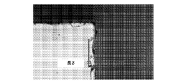
切断後、ガラスウェハー1は、図2に図示されるように新たな切断エッジ10を有する。この切断エッジ10は通常は、第1の切断プロセスの結果としてある程度のエッジチッピング11を示す。このようなエッジチッピング11によって例えば伝播クラックが生じる可能性があり、こうしたクラックによって、切断やさらなる処理の間に最終的にはガラスウェハー1の破損が生じる。さらにエッジチッピング11によって、ダイシング後に有効に利用することのできる領域Aが減少する。したがって、エッジチッピング11を低減することによって、ダイシング歩留まりを高めることができる。総じて、特徴的な最大エッジチッピングサイズCを特定することができ、これは例えば、使用する切断ブレードや他の切断パラメーター、例えばブレードの送り速度や回転速度に依存する。しかし所与の切断パラメーターセットについて、ガラスウェハー1に特定のガラス材料を使用することによって、最大エッジチッピングサイズCを低減することができる。
After cutting, the
したがって本発明によるガラス製のガラスウェハー1によって、エッジチッピングの傾向が低くなり、したがって以下の例から分かるように高いダイシング歩留まりが可能となる。
The
例
以下の表1に、本発明による11個の例示的なガラス組成を示す。例12~14に、本発明の範囲に包含されない例示的な比較ガラスを示す。例1~5および7~11には無アルカリガラスの組成を示し、例6にはアルカリ含有ガラスを記載する。
Examples Table 1 below shows eleven exemplary glass compositions according to the present invention. Examples 12-14 provide exemplary comparative glasses not within the scope of the present invention. Examples 1-5 and 7-11 show compositions of alkali-free glasses, and Example 6 describes an alkali-containing glass.

以下の表2に、表1による例1~11および比較例12~14のガラス組成の選択された関連パラメーターを列挙する。 Table 2 below lists selected relevant parameters of the glass compositions of Examples 1-11 and Comparative Examples 12-14 according to Table 1.

本発明によるこれらの例1~11は、(丸められた)-0.2から-0.12までのNBO数の範囲にわたっている。この場合のB2O3/Al2O3の比は、(丸められた)0.6から約1.6までの範囲にある。ガラス転移温度は、(丸められた)560℃から715℃までの範囲にある。表2から分かるように、すべてのガラス試料1~11のビッカース硬さHVは、(丸められた)5255MPaから5725MPaまでの範囲にあり、破壊靭性KICは、0.45MPa・m1/2から0.88MPa・m1/2までの範囲にある。得られる脆性はHV/KICとして定義され、これは6.5μm-1/2から11.9μm-1/2までの範囲にある。 These Examples 1-11 according to the invention span a range of NBO numbers from -0.2 (rounded) to -0.12. The B 2 O 3 /Al 2 O 3 ratio in this case ranges from 0.6 (rounded) to about 1.6. The glass transition temperatures range from 560°C (rounded) to 715°C. As can be seen from Table 2, the Vickers hardness H V of all glass samples 1-11 ranged from 5255 MPa (rolled) to 5725 MPa, and the fracture toughness K IC was 0.45 MPa m 1/2 to 0.88 MPa·m 1/2 . The resulting brittleness is defined as H V /K IC , which ranges from 6.5 μm −1/2 to 11.9 μm −1/2 .
比較例12~14は、-0.2未満のNBO数および0.5未満の比B2O3/Al2O3を有する。 Comparative Examples 12-14 have NBO numbers less than -0.2 and ratios B 2 O 3 /Al 2 O 3 less than 0.5.
表2にはまた、ガラス試料の切断時に得られたチッピング性能を右端の欄に示す。図2に図示されるように、ここでの「チッピングサイズ」とは、最大チッピングサイズCを指す。試料を、直径56mm、幅w1 0.15mmのソフト600メッシュダイシングブレードで、送り速度5mm/s、回転速度20krpmで切断した。チッピング性能は、これらのダイシングパラメーターにはそれほど依存しないことが判明し、当技術分野で例えばWLP用途で通常適用される範囲のダイシングパラメーターの場合と同等の結果が認められた。 Table 2 also shows the chipping performance obtained when cutting glass samples in the far right column. The term "chipping size" herein refers to the maximum chipping size C, as illustrated in FIG. The samples were cut with a soft 600 mesh dicing blade with a diameter of 56 mm and a width w 1 of 0.15 mm at a feed rate of 5 mm/s and a rotation speed of 20 krpm. Chipping performance was found to be less dependent on these dicing parameters, and comparable results were observed for dicing parameter ranges typically applied in the art, eg, for WLP applications.
ガラス試料の厚さtは、例1~14のすべてのガラス組成物について0.5mmであった。-0.2以上の値であるいずれのNBO数についても、得られる最大エッジチッピングサイズは30μm以下であるのに対して、比較例12~14の最大エッジチッピングサイズは30μmを上回ることが明らかに見て取れる。 The thickness t of the glass samples was 0.5 mm for all glass compositions of Examples 1-14. It is clear that for any NBO number of -0.2 or greater, the maximum edge chipping size obtained is 30 μm or less, whereas the maximum edge chipping size of Comparative Examples 12-14 is greater than 30 μm. I can see it.
図3に、NBO数に対する脆性HV/KICの値を示し、一方で図4に、チッピングサイズについての相応する値を示す。図5および図6に、B2O3/Al2O3の比に対する相応するグラフを示す。いずれのプロットからも、関連するパラメーターであるNBOおよびB2O3/Al2O3に応じて脆性およびチッピングサイズが減少する傾向にあることが明らかに示されており、-0.2のNBO値および0.5の比B2O3/Al2O3で、脆性指数HV/KICが12μm-1/2(破線)を上回る値からこれを下回る値へと移行し、最大チッピングサイズが30μm(破線)を上回る値からこれを下回る値へと移行する。 FIG. 3 shows the values of brittleness H V /K IC versus NBO number, while FIG. 4 shows the corresponding values for chipping size. 5 and 6 show corresponding graphs for the B 2 O 3 /Al 2 O 3 ratio. Both plots clearly show a decreasing trend in brittleness and chipping size with the relevant parameters NBO and B2O3 / Al2O3 , with an NBO of -0.2. and a ratio B 2 O 3 /Al 2 O 3 of 0.5, the brittleness index H V /K IC transitions from values above 12 μm −1/2 (dashed line) to values below it and the maximum chipping size transitions from values above 30 μm (dashed line) to values below.
図7~9に、表1による例7、9および10の選択された試料の切断ブレードの拡大図を示す。図7に、NBOが-0.162である例7によるガラスの試料を示す。この図から分かるように、最大エッジチッピングサイズは14.42μmであり、これは、表2では14μmに丸められている。同様に図8には、表1の例9によるガラスの試料を示す。これは、NBOが-0.140であり、得られた最大エッジチッピングサイズが12.25μmである。図9に、例10によるガラスの試料を示す。これは、NBOが-0.129であり、最大エッジチッピングサイズが9.48μmである。これに対応する表2の最大エッジチッピングサイズの値は、それぞれ最も近い整数に丸めたものである。 7-9 show enlarged views of the cutting blades of selected samples of Examples 7, 9 and 10 according to Table 1. FIG. FIG. 7 shows a sample of glass according to Example 7 with an NBO of −0.162. As can be seen from this figure, the maximum edge chipping size is 14.42 μm, which is rounded to 14 μm in Table 2. Similarly, FIG. 8 shows a sample of glass according to Example 9 of Table 1. It has an NBO of −0.140 and a maximum edge chipping size obtained of 12.25 μm. A sample of the glass according to Example 10 is shown in FIG. It has an NBO of −0.129 and a maximum edge chipping size of 9.48 μm. The corresponding maximum edge chipping size values in Table 2 are each rounded to the nearest integer.
Claims (17)

多面体1つあたりの非架橋酸素の平均数(NBO)は、-0.2以上であり、比B2O3/Al2O3は、0.5以上であり、ここで、前記NBOは、NBO=2×Omol/(Simol+Almol+Bmol)-4と定義される、前記低CTEボロアルミノシリケートガラス製のガラスキャリアウェハー。 Composition in mol % of:
The average number of non-bridging oxygens per polyhedron (NBO) is greater than or equal to −0.2 and the ratio B 2 O 3 /Al 2 O 3 is greater than or equal to 0.5, wherein said NBO is A glass carrier wafer made of said low CTE boro-aluminosilicate glass, defined as NBO=2×O mol /(Si mol +Al mol +B mol )−4.

Priority Applications (1)
| Application Number | Priority Date | Filing Date | Title |
|---|---|---|---|
| JP2020089132A JP7184845B2 (en) | 2020-05-21 | 2020-05-21 | Low CTE boro-aluminosilicate glass for glass carrier wafer |
Applications Claiming Priority (1)
| Application Number | Priority Date | Filing Date | Title |
|---|---|---|---|
| JP2020089132A JP7184845B2 (en) | 2020-05-21 | 2020-05-21 | Low CTE boro-aluminosilicate glass for glass carrier wafer |
Related Parent Applications (1)
| Application Number | Title | Priority Date | Filing Date |
|---|---|---|---|
| JP2018540104A Division JP6708746B2 (en) | 2016-02-02 | 2016-02-02 | Low CTE boroaluminosilicate glass for glass carrier wafers |
Publications (2)
| Publication Number | Publication Date |
|---|---|
| JP2020128339A JP2020128339A (en) | 2020-08-27 |
| JP7184845B2 true JP7184845B2 (en) | 2022-12-06 |
Family
ID=72175311
Family Applications (1)
| Application Number | Title | Priority Date | Filing Date |
|---|---|---|---|
| JP2020089132A Active JP7184845B2 (en) | 2020-05-21 | 2020-05-21 | Low CTE boro-aluminosilicate glass for glass carrier wafer |
Country Status (1)
| Country | Link |
|---|---|
| JP (1) | JP7184845B2 (en) |
Families Citing this family (1)
| Publication number | Priority date | Publication date | Assignee | Title |
|---|---|---|---|---|
| CN113053798A (en) * | 2021-03-30 | 2021-06-29 | 绍兴同芯成集成电路有限公司 | Ultrathin crystal thinning and cutting process utilizing tempered glass |
Citations (10)
| Publication number | Priority date | Publication date | Assignee | Title |
|---|---|---|---|---|
| JP2002201040A (en) | 2000-10-31 | 2002-07-16 | Asahi Glass Co Ltd | Aluminoborosilicate glass |
| JP2005302289A (en) | 2005-05-18 | 2005-10-27 | Hoya Corp | Glass substrate for information recording medium and magnetic information recording medium using the same |
| JP2007269625A (en) | 2006-03-31 | 2007-10-18 | Schott Ag | Aluminoborosilicate glass |
| JP2008001589A (en) | 2006-05-23 | 2008-01-10 | Nippon Electric Glass Co Ltd | Alkali-free glass, alkali-free glass substrate, and its manufacturing method |
| JP2009013049A (en) | 2007-06-08 | 2009-01-22 | Nippon Electric Glass Co Ltd | Alkali-free glass and alkali-free glass substrate |
| JP2009177034A (en) | 2008-01-26 | 2009-08-06 | Fujikura Ltd | Method for manufacturing semiconductor package |
| WO2011136027A1 (en) | 2010-04-27 | 2011-11-03 | 旭硝子株式会社 | Method for producing magnetic disk and method for producing glass substrate for information recording medium |
| JP2014527299A (en) | 2011-08-04 | 2014-10-09 | コーニング インコーポレイテッド | Photovoltaic module package |
| WO2015091134A1 (en) | 2013-12-17 | 2015-06-25 | Schott Ag | Glass that can be chemically strengthened and glass element produced therefrom |
| JP2016117641A (en) | 2014-12-17 | 2016-06-30 | 日本電気硝子株式会社 | Support glass substrate and laminate comprising the same |
-
2020
- 2020-05-21 JP JP2020089132A patent/JP7184845B2/en active Active
Patent Citations (11)
| Publication number | Priority date | Publication date | Assignee | Title |
|---|---|---|---|---|
| JP2002201040A (en) | 2000-10-31 | 2002-07-16 | Asahi Glass Co Ltd | Aluminoborosilicate glass |
| JP2005302289A (en) | 2005-05-18 | 2005-10-27 | Hoya Corp | Glass substrate for information recording medium and magnetic information recording medium using the same |
| JP2007269625A (en) | 2006-03-31 | 2007-10-18 | Schott Ag | Aluminoborosilicate glass |
| JP2008001589A (en) | 2006-05-23 | 2008-01-10 | Nippon Electric Glass Co Ltd | Alkali-free glass, alkali-free glass substrate, and its manufacturing method |
| JP2009013049A (en) | 2007-06-08 | 2009-01-22 | Nippon Electric Glass Co Ltd | Alkali-free glass and alkali-free glass substrate |
| JP2009177034A (en) | 2008-01-26 | 2009-08-06 | Fujikura Ltd | Method for manufacturing semiconductor package |
| WO2011136027A1 (en) | 2010-04-27 | 2011-11-03 | 旭硝子株式会社 | Method for producing magnetic disk and method for producing glass substrate for information recording medium |
| JP2014527299A (en) | 2011-08-04 | 2014-10-09 | コーニング インコーポレイテッド | Photovoltaic module package |
| WO2015091134A1 (en) | 2013-12-17 | 2015-06-25 | Schott Ag | Glass that can be chemically strengthened and glass element produced therefrom |
| JP2016540721A (en) | 2013-12-17 | 2016-12-28 | ショット アクチエンゲゼルシャフトSchott AG | Chemically temperable glass and glass elements made therefrom |
| JP2016117641A (en) | 2014-12-17 | 2016-06-30 | 日本電気硝子株式会社 | Support glass substrate and laminate comprising the same |
Also Published As
| Publication number | Publication date |
|---|---|
| JP2020128339A (en) | 2020-08-27 |
Similar Documents
| Publication | Publication Date | Title |
|---|---|---|
| US11059738B2 (en) | Low CTE boro-aluminosilicate glass for glass carrier wafers | |
| JP6593669B2 (en) | Support glass substrate and carrier using the same | |
| KR102561430B1 (en) | Supporting glass substrate and laminated body | |
| WO2015156075A1 (en) | Supporting glass substrate and laminate using same | |
| WO2016035674A1 (en) | Supporting glass substrate and laminate using same | |
| JP6443668B2 (en) | Support glass substrate and laminate using the same | |
| WO2017104514A1 (en) | Crystallized glass support substrate and laminate body using same | |
| JP2016117641A (en) | Support glass substrate and laminate comprising the same | |
| JP7184845B2 (en) | Low CTE boro-aluminosilicate glass for glass carrier wafer | |
| CN116813198A (en) | Support glass substrate and laminate using same | |
| JP2016155736A (en) | Support glass substrate and laminate using the same | |
| CN107108318B (en) | Glass plate and method for producing same | |
| CN114728838B (en) | Chemically strengthened glass and glass ceramics, and methods for producing same | |
| JP2016155735A (en) | Support glass substrate and laminate using the same | |
| JP7538483B2 (en) | Support glass substrate and laminated substrate using same | |
| TW201837975A (en) | Crystallized glass support substrate and laminate using same | |
| JP2022523029A (en) | Glass-ceramic articles, compositions, and methods of manufacturing them. | |
| JP2018095514A (en) | Glass support substrate and laminate using same | |
| WO2024197657A1 (en) | High young's modulus glass material and article produced using the glass | |
| WO2018110163A1 (en) | Glass support substrate and laminate using same | |
| WO2016098499A1 (en) | Support glass substrate and laminate using same | |
| JP2020045281A (en) | Glass plate |
Legal Events
| Date | Code | Title | Description |
|---|---|---|---|
| A521 | Request for written amendment filed |
Free format text: JAPANESE INTERMEDIATE CODE: A523 Effective date: 20200619 |
|
| A621 | Written request for application examination |
Free format text: JAPANESE INTERMEDIATE CODE: A621 Effective date: 20200619 |
|
| A131 | Notification of reasons for refusal |
Free format text: JAPANESE INTERMEDIATE CODE: A131 Effective date: 20210510 |
|
| RD03 | Notification of appointment of power of attorney |
Free format text: JAPANESE INTERMEDIATE CODE: A7423 Effective date: 20210719 |
|
| A521 | Request for written amendment filed |
Free format text: JAPANESE INTERMEDIATE CODE: A523 Effective date: 20210729 |
|
| A131 | Notification of reasons for refusal |
Free format text: JAPANESE INTERMEDIATE CODE: A131 Effective date: 20220105 |
|
| A521 | Request for written amendment filed |
Free format text: JAPANESE INTERMEDIATE CODE: A523 Effective date: 20220328 |
|
| A02 | Decision of refusal |
Free format text: JAPANESE INTERMEDIATE CODE: A02 Effective date: 20220705 |
|
| A521 | Request for written amendment filed |
Free format text: JAPANESE INTERMEDIATE CODE: A523 Effective date: 20221024 |
|
| C60 | Trial request (containing other claim documents, opposition documents) |
Free format text: JAPANESE INTERMEDIATE CODE: C60 Effective date: 20221024 |
|
| A911 | Transfer to examiner for re-examination before appeal (zenchi) |
Free format text: JAPANESE INTERMEDIATE CODE: A911 Effective date: 20221031 |
|
| C21 | Notice of transfer of a case for reconsideration by examiners before appeal proceedings |
Free format text: JAPANESE INTERMEDIATE CODE: C21 Effective date: 20221108 |
|
| TRDD | Decision of grant or rejection written | ||
| A01 | Written decision to grant a patent or to grant a registration (utility model) |
Free format text: JAPANESE INTERMEDIATE CODE: A01 Effective date: 20221116 |
|
| A61 | First payment of annual fees (during grant procedure) |
Free format text: JAPANESE INTERMEDIATE CODE: A61 Effective date: 20221124 |
|
| R150 | Certificate of patent or registration of utility model |
Ref document number: 7184845 Country of ref document: JP Free format text: JAPANESE INTERMEDIATE CODE: R150 |