JP7176662B1 - Semiconductor equipment and power conversion equipment - Google Patents

Semiconductor equipment and power conversion equipment Download PDF

Info

Publication number
JP7176662B1
JP7176662B1 JP2022518732A JP2022518732A JP7176662B1 JP 7176662 B1 JP7176662 B1 JP 7176662B1 JP 2022518732 A JP2022518732 A JP 2022518732A JP 2022518732 A JP2022518732 A JP 2022518732A JP 7176662 B1 JP7176662 B1 JP 7176662B1
Authority
JP
Japan
Prior art keywords
electrode
semiconductor device
covering portion
wiring
covering
Prior art date
Legal status (The legal status is an assumption and is not a legal conclusion. Google has not performed a legal analysis and makes no representation as to the accuracy of the status listed.)
Active
Application number
JP2022518732A
Other languages
Japanese (ja)
Other versions
JPWO2023079640A1 (en
JPWO2023079640A5 (en
Inventor
隆一郎 花田
誠次 岡
啓行 原田
Current Assignee (The listed assignees may be inaccurate. Google has not performed a legal analysis and makes no representation or warranty as to the accuracy of the list.)
Mitsubishi Electric Corp
Original Assignee
Mitsubishi Electric Corp
Priority date (The priority date is an assumption and is not a legal conclusion. Google has not performed a legal analysis and makes no representation as to the accuracy of the date listed.)
Filing date
Publication date
Application filed by Mitsubishi Electric Corp filed Critical Mitsubishi Electric Corp
Application granted granted Critical
Publication of JP7176662B1 publication Critical patent/JP7176662B1/en
Publication of JPWO2023079640A1 publication Critical patent/JPWO2023079640A1/ja
Publication of JPWO2023079640A5 publication Critical patent/JPWO2023079640A5/ja
Active legal-status Critical Current
Anticipated expiration legal-status Critical

Links

Images

Classifications

    • HELECTRICITY
    • H01ELECTRIC ELEMENTS
    • H01LSEMICONDUCTOR DEVICES NOT COVERED BY CLASS H10
    • H01L21/00Processes or apparatus adapted for the manufacture or treatment of semiconductor or solid state devices or of parts thereof
    • H01L21/02Manufacture or treatment of semiconductor devices or of parts thereof
    • H01L21/04Manufacture or treatment of semiconductor devices or of parts thereof the devices having at least one potential-jump barrier or surface barrier, e.g. PN junction, depletion layer or carrier concentration layer
    • H01L21/50Assembly of semiconductor devices using processes or apparatus not provided for in a single one of the subgroups H01L21/06 - H01L21/326, e.g. sealing of a cap to a base of a container
    • H01L21/60Attaching or detaching leads or other conductive members, to be used for carrying current to or from the device in operation
    • HELECTRICITY
    • H01ELECTRIC ELEMENTS
    • H01LSEMICONDUCTOR DEVICES NOT COVERED BY CLASS H10
    • H01L23/00Details of semiconductor or other solid state devices
    • H01L23/48Arrangements for conducting electric current to or from the solid state body in operation, e.g. leads, terminal arrangements ; Selection of materials therefor
    • HELECTRICITY
    • H01ELECTRIC ELEMENTS
    • H01LSEMICONDUCTOR DEVICES NOT COVERED BY CLASS H10
    • H01L25/00Assemblies consisting of a plurality of individual semiconductor or other solid state devices ; Multistep manufacturing processes thereof
    • H01L25/03Assemblies consisting of a plurality of individual semiconductor or other solid state devices ; Multistep manufacturing processes thereof all the devices being of a type provided for in the same subgroup of groups H01L27/00 - H01L33/00, or in a single subclass of H10K, H10N, e.g. assemblies of rectifier diodes
    • H01L25/04Assemblies consisting of a plurality of individual semiconductor or other solid state devices ; Multistep manufacturing processes thereof all the devices being of a type provided for in the same subgroup of groups H01L27/00 - H01L33/00, or in a single subclass of H10K, H10N, e.g. assemblies of rectifier diodes the devices not having separate containers
    • H01L25/07Assemblies consisting of a plurality of individual semiconductor or other solid state devices ; Multistep manufacturing processes thereof all the devices being of a type provided for in the same subgroup of groups H01L27/00 - H01L33/00, or in a single subclass of H10K, H10N, e.g. assemblies of rectifier diodes the devices not having separate containers the devices being of a type provided for in group H01L29/00
    • HELECTRICITY
    • H01ELECTRIC ELEMENTS
    • H01LSEMICONDUCTOR DEVICES NOT COVERED BY CLASS H10
    • H01L25/00Assemblies consisting of a plurality of individual semiconductor or other solid state devices ; Multistep manufacturing processes thereof
    • H01L25/18Assemblies consisting of a plurality of individual semiconductor or other solid state devices ; Multistep manufacturing processes thereof the devices being of types provided for in two or more different subgroups of the same main group of groups H01L27/00 - H01L33/00, or in a single subclass of H10K, H10N

Abstract

半導体素子の表面の電極上に開口部を有する被覆部を形成することで、配線部の接合性を損なうことなく、半導体素子の電極と封止部との応力緩和を行うことで、信頼性を向上させた半導体装置を得ることができる。上面に電極(13)を有する半導体素子(7)と、開口部(40)を有して電極(13)の表面に配置された被覆部(30)と、被覆部(30)の開口部(40)の内周部と間隔を空けて開口部(40)内に配置された配線部(9)と、被覆部(30)と配線部(9)と半導体素子(7)とを封止する封止部(10)と、を備えた半導体装置である。By forming a covering portion having an opening on the electrode on the surface of the semiconductor element, the stress between the electrode of the semiconductor element and the sealing portion is relieved without impairing the bonding of the wiring portion, thereby improving reliability. An improved semiconductor device can be obtained. A semiconductor element (7) having an electrode (13) on its upper surface, a cover (30) having an opening (40) and disposed on the surface of the electrode (13), and an opening ( 40), the wiring portion (9) arranged in the opening (40) with a space therebetween, the covering portion (30), the wiring portion (9), and the semiconductor element (7) are sealed. A semiconductor device comprising a sealing portion (10).

Description

本開示は、半導体素子の表面の電極に被覆部を形成した半導体装置および電力変換装置に関する。 The present disclosure relates to a semiconductor device and a power conversion device in which a cover is formed on an electrode on the surface of a semiconductor element.

半導体装置に実装される半導体素子と導電ワイヤとには、それぞれの熱膨張係数の差に起因して、半導体装置の動作中に半導体素子と導電ワイヤとの接合部に繰り返し応力が印加される。この応力により、半導体素子と導電ワイヤとの接合部にクラックが発生し、半導体素子と導電ワイヤとの接合部が剥離することで、半導体装置の信頼性が低下するという課題があった。 Due to the difference in coefficient of thermal expansion between the semiconductor element and the conductive wire mounted on the semiconductor device, stress is repeatedly applied to the junction between the semiconductor element and the conductive wire during operation of the semiconductor device. This stress causes cracks in the joints between the semiconductor elements and the conductive wires, and the joints between the semiconductor elements and the conductive wires are peeled off, thereby reducing the reliability of the semiconductor device.

この課題解決のために、半導体素子と導電ワイヤとの接合部での応力緩和を目的として、半導体素子と導電ワイヤとの接合部の周囲を樹脂で被覆する構造(例えば、特許文献1、特許文献2)、または半導体素子の表面に選択的に絶縁性厚膜を形成する構造(例えば、特許文献3)が検討されている。 In order to solve this problem, for the purpose of stress relaxation at the junction between the semiconductor element and the conductive wire, a structure in which the periphery of the junction between the semiconductor element and the conductive wire is covered with a resin (for example, Patent Document 1, Patent Document 2), or a structure in which a thick insulating film is selectively formed on the surface of a semiconductor element (for example, Patent Document 3).

半導体素子の熱膨張係数と導電ワイヤの熱膨張係数との間の差に起因して、パワー半導体装置の使用中に、半導体素子と導電ワイヤとの間の接合部に応力が繰り返し印加される。これにより半導体素子と導電ワイヤとの間の接合部にクラックが発生し信頼性が低下するという課題があり、これに対して接合部周囲を樹脂で被覆することで応力を緩和する試みが行われてきた。 Due to the difference between the thermal expansion coefficients of the semiconductor element and the conductive wire, stress is repeatedly applied to the joint between the semiconductor element and the conductive wire during use of the power semiconductor device. As a result, there is a problem that cracks occur in the junction between the semiconductor element and the conductive wire, reducing reliability, and attempts have been made to alleviate the stress by coating the periphery of the junction with resin. It's here.

特開平6―120284号公報JP-A-6-120284 国際公開第2016/016970号WO2016/016970 特開2003―273357号公報JP-A-2003-273357

しかしながら、特許文献1に記載の半導体装置においては、半導体素子上に導電ワイヤを形成後に、半導体素子と導電ワイヤとの接合部の周囲へ樹脂を形成しているが、ボンディングパットには樹脂は形成されていない。また、特許文献2に記載の半導体装置においては、表面電極上を樹脂で覆っているものの、被覆性を考慮して樹脂の粘性を低くしているので、樹脂の不必要な拡散を防止するために拡散防止用の部材が必要であった。さらに、特許文献3に記載の半導体装置においては、半導体素子の反りを抑制するために半導体素子上に樹脂を形成しているが、特に、導電ワイヤとの接合部に対する対応は行われてはいない。このため、半導体素子と導電ワイヤとの接合部での応力緩和効果が弱く、半導体装置の信頼性が劣化する場合があった。 However, in the semiconductor device described in Patent Document 1, after forming the conductive wire on the semiconductor element, the resin is formed around the bonding portion between the semiconductor element and the conductive wire, but the resin is not formed on the bonding pad. It has not been. In addition, in the semiconductor device described in Patent Document 2, although the surface electrodes are covered with a resin, the viscosity of the resin is lowered in consideration of the coverage, so that unnecessary diffusion of the resin can be prevented. required a member to prevent diffusion. Furthermore, in the semiconductor device described in Patent Document 3, a resin is formed on the semiconductor element in order to suppress warping of the semiconductor element, but no particular measures are taken for the junction with the conductive wire. . Therefore, the stress relaxation effect at the junction between the semiconductor element and the conductive wire is weak, and the reliability of the semiconductor device may be deteriorated.

本開示は、上述のような問題を解決するためになされたもので、半導体素子と導電ワイヤとの接合部に対して隙間を空けて被覆部を配置することで、半導体素子と導電ワイヤとの接合部での応力を緩和し、信頼性の向上した半導体素子を得ることを目的としている。 The present disclosure has been made to solve the above-described problems, and by arranging a covering portion with a gap with respect to the joint portion between the semiconductor element and the conductive wire, the semiconductor element and the conductive wire are separated from each other. An object of the present invention is to obtain a semiconductor device with improved reliability by alleviating the stress at the junction.

本開示に係る半導体装置は、上面に電極を有する半導体素子と、開口部を有して電極の表面を被覆する被覆部と、被覆部の開口部の内周部と間隔を空けて開口部内に配置されたワイヤである配線部と、被覆部と配線部と半導体素子とを封止する封止部と、を備え、開口部は、電極と配線部との接合部の周囲に電極が被覆部で被覆されないよう隙間を開けるように配置されることを特徴とする半導体装置である。 A semiconductor device according to the present disclosure includes a semiconductor element having an electrode on the upper surface , a covering portion having an opening and covering the surface of the electrode, and a semiconductor device in the opening spaced apart from the inner peripheral portion of the opening of the covering portion. and a sealing portion that seals the covering portion, the wiring portion, and the semiconductor element . The semiconductor device is characterized in that it is arranged so as to leave a gap so as not to be covered with a film .

本開示によれば、半導体素子の上面の電極上に、配線部と間隔を空けて被覆部を配置したので、半導体素子の電極と配線部との接合部における応力を緩和することができ、配線部の電極からの剥離を抑制することが可能となり、半導体装置の信頼性を向上させることができる。 According to the present disclosure, since the covering portion is arranged on the electrode on the upper surface of the semiconductor element with a gap from the wiring portion, the stress in the joint portion between the electrode of the semiconductor element and the wiring portion can be relieved. It becomes possible to suppress peeling of the portion from the electrode, and the reliability of the semiconductor device can be improved.

実施の形態1における半導体装置を示す平面構造模式図である。1 is a schematic plan view showing a semiconductor device according to a first embodiment; FIG. 実施の形態1における半導体装置を示す断面構造模式図である。1 is a cross-sectional structural schematic diagram showing a semiconductor device according to a first embodiment; FIG. 実施の形態1における半導体装置の配線部の接合部を拡大して示す断面構造模式図である。FIG. 2 is a cross-sectional structural schematic diagram showing an enlarged joint portion of a wiring portion of the semiconductor device in Embodiment 1; 実施の形態1における半導体装置の被覆部を示す平面構造模式図である。2 is a schematic plan view showing a covering portion of the semiconductor device according to Embodiment 1; FIG. 実施の形態1における半導体装置の被覆部を示す斜視構造模式図である。2 is a perspective structural schematic diagram showing a covering portion of the semiconductor device according to the first embodiment; FIG. 実施の形態1における半導体装置の他の被覆部を示す平面構造模式図である。3 is a schematic plan view showing another covering portion of the semiconductor device according to the first embodiment; FIG. 実施の形態1における半導体装置の他の被覆部を示す平面構造模式図である。3 is a schematic plan view showing another covering portion of the semiconductor device according to the first embodiment; FIG. 実施の形態1における半導体装置の他の被覆部を示す平面構造模式図である。3 is a schematic plan view showing another covering portion of the semiconductor device according to the first embodiment; FIG. 実施の形態1における半導体装置の他の被覆部を示す平面構造模式図である。3 is a schematic plan view showing another covering portion of the semiconductor device according to the first embodiment; FIG. 実施の形態1における半導体装置の他の被覆部を示す斜視構造模式図である。FIG. 10 is a perspective structural schematic diagram showing another covering portion of the semiconductor device in Embodiment 1; 実施の形態1における半導体装置の他の被覆部を示す斜視構造模式図である。FIG. 10 is a perspective structural schematic diagram showing another covering portion of the semiconductor device in Embodiment 1; 実施の形態2における半導体装置を示す平面構造模式図である。FIG. 10 is a schematic plan view showing a semiconductor device according to a second embodiment; 実施の形態2における半導体装置を示す断面構造模式図である。FIG. 10 is a schematic cross-sectional view showing a semiconductor device according to a second embodiment; 実施の形態2における半導体装置の配線部の接合部を拡大して示す断面構造模式図である。FIG. 10 is a cross-sectional structural schematic diagram showing an enlarged joint portion of a wiring portion of a semiconductor device according to a second embodiment; 実施の形態3における電力変換装置を適用した電力変換システムの構成を示すブロック図である。FIG. 12 is a block diagram showing the configuration of a power conversion system to which a power conversion device according to Embodiment 3 is applied;

はじめに、本開示の半導体装置の全体構成について、図面を参照しながら説明する。なお、図は模式的なものであり、示された構成要素の正確な大きさなどを反映するものではない。また、同一の符号を付したものは、同一又はこれに相当するものであり、このことは明細書の全文において共通することである。 First, the overall configuration of the semiconductor device of the present disclosure will be described with reference to the drawings. It should be noted that the figures are schematic and do not reflect the exact sizes of the components shown. Also, the same reference numerals denote the same or corresponding parts, and this is common throughout the specification.

実施の形態1.
図1は、実施の形態1における半導体装置を示す平面構造模式図である。図2は、実施の形態1における半導体装置を示す断面構造模式図である。図3は、実施の形態1における半導体装置の配線部の接合部を拡大して示す断面構造模式図である。図において、半導体装置100は、ベース板1と、絶縁基板2と、接合部である素子接合部8と、接合部である基板接合部3と、半導体素子7と、配線部である9と、封止部10と、電極端子12と、電極13と、被覆部30と、被覆部30で囲まれた開口部40と、を備えている。なお、図2は、図1の一点鎖線AAにおける断面構造模式図である。
Embodiment 1.
FIG. 1 is a schematic plan view showing a semiconductor device according to Embodiment 1. FIG. FIG. 2 is a schematic cross-sectional view showing the semiconductor device according to the first embodiment. FIG. 3 is a cross-sectional structural schematic diagram showing an enlarged junction portion of the wiring portion of the semiconductor device according to the first embodiment. In the figure, a semiconductor device 100 includes a base plate 1, an insulating substrate 2, an element bonding portion 8 that is a bonding portion, a substrate bonding portion 3 that is a bonding portion, a semiconductor element 7, a wiring portion 9, It includes a sealing portion 10 , an electrode terminal 12 , an electrode 13 , a covering portion 30 , and an opening portion 40 surrounded by the covering portion 30 . In addition, FIG. 2 is a cross-sectional structure schematic diagram in the dashed-dotted line AA of FIG.

図において、半導体装置100は、ベース板1の上面と絶縁基板2の下面とを基板接合部3を用いて接合している。絶縁基板2の上面と半導体素子7の裏面(下面)とを素子接合部8を用いて接合している。絶縁基板2と絶縁基板2の上面に接合された半導体素子7と配線部9とは、封止部10内に封止されている。 In the figure, the semiconductor device 100 has the upper surface of the base plate 1 and the lower surface of the insulating substrate 2 joined together using the substrate joining portion 3 . The upper surface of the insulating substrate 2 and the back surface (lower surface) of the semiconductor element 7 are bonded using the element bonding portion 8 . The insulating substrate 2 and the semiconductor element 7 and the wiring portion 9 bonded to the upper surface of the insulating substrate 2 are sealed in the sealing portion 10 .

図1において、封止部10は、点線にて表示し、封止部10に封止されている部材の位置関係がわかるようにしている。半導体装置100の最外周は、ベース板1の周縁部である。ベース板1の周縁部よりも内側には、封止部10が配置されている。封止部10の外縁よりも内側には、絶縁基板2の絶縁層22が配置されている。絶縁基板2の絶縁層22の外縁よりも内側には、絶縁基板2の上面側の金属層21が配置されている。絶縁基板2の上面側の金属層21の外縁よりも内側には、電極13が表面に形成された半導体素子7が配置されている。半導体素子7の電極13の外縁よりも内側には、開口部40を有する被覆部30が配置されている。開口部40は、所定の幅を有する被覆部30に囲まれた領域である。被覆部30の内縁よりも内側には、被覆部30の内縁と間隔を開けて配線部9が電極13と接合されている。電極端子12は、絶縁基板2を跨いで配置され、封止部10から突出(露出)している。 In FIG. 1, the sealing portion 10 is indicated by a dotted line so that the positional relationship of the members sealed in the sealing portion 10 can be understood. The outermost periphery of the semiconductor device 100 is the periphery of the base plate 1 . A sealing portion 10 is arranged inside the peripheral portion of the base plate 1 . An insulating layer 22 of the insulating substrate 2 is arranged inside the outer edge of the sealing portion 10 . The metal layer 21 on the upper surface side of the insulating substrate 2 is arranged inside the outer edge of the insulating layer 22 of the insulating substrate 2 . A semiconductor element 7 having an electrode 13 formed thereon is arranged inside the outer edge of the metal layer 21 on the upper surface side of the insulating substrate 2 . A covering portion 30 having an opening 40 is arranged inside the outer edge of the electrode 13 of the semiconductor element 7 . The opening 40 is a region surrounded by the covering portion 30 having a predetermined width. Inside the inner edge of the covering portion 30 , the wiring portion 9 is joined to the electrode 13 with a gap from the inner edge of the covering portion 30 . The electrode terminal 12 is arranged across the insulating substrate 2 and protrudes (exposed) from the sealing portion 10 .

図2において、ベース板1の上面と絶縁基板2の下面側の金属層23の下面とを基板接合部3を用いて接合している。絶縁基板2の上面側の金属層21の上面と半導体素子7の裏面とを素子接合部8を用いて接合している。配線部9は、半導体素子7の表面(上面)の電極13と電極端子12(右側)とを電気的に接続している。また、配線部であるボンディングワイヤ9は、絶縁基板2の上面側の金属層21の所定の位置と電極端子12(左側)とを電気的に接続している。封止部10は、絶縁基板2の下面側の金属層23と接合していない(露出した)ベース板1の上面と接して、絶縁基板2と絶縁基板2の上面に接合された半導体素子7とを封止している。電極端子12は、絶縁基板2の上部で、一端側が封止部10内に配置され、他端が封止部10の側面から露出(突出)して配置される。 In FIG. 2, the upper surface of the base plate 1 and the lower surface of the metal layer 23 on the lower surface side of the insulating substrate 2 are joined using the substrate joint portion 3 . The upper surface of the metal layer 21 on the upper surface side of the insulating substrate 2 and the back surface of the semiconductor element 7 are bonded using the element bonding portion 8 . The wiring portion 9 electrically connects the electrode 13 on the surface (upper surface) of the semiconductor element 7 and the electrode terminal 12 (on the right side). A bonding wire 9, which is a wiring portion, electrically connects a predetermined position of the metal layer 21 on the upper surface side of the insulating substrate 2 and the electrode terminal 12 (left side). The sealing portion 10 is in contact with the upper surface of the base plate 1 that is not bonded (exposed) to the metal layer 23 on the lower surface side of the insulating substrate 2 , and the insulating substrate 2 and the semiconductor element 7 bonded to the upper surface of the insulating substrate 2 . and are sealed. The electrode terminal 12 is arranged above the insulating substrate 2 so that one end side is arranged inside the sealing portion 10 and the other end side is exposed (protrudes) from the side surface of the sealing portion 10 .

図3において、半導体素子7の表面に配置された電極13と配線部9とは、接合部31で接合されている。被覆部30は、接合部31を囲んでいる。被覆部30で囲まれた内側は、開口部40である。接合部31の外縁(外周部)と被覆部30の内縁(内周部)とは隙間(間隔)Sを開けて配置される。封止部10は、隙間Sの部分では、電極13の表面と接して配置されている。また、封止部10は、隙間Sよりも外側(被覆部30の内縁よりも外側)では、被覆部30の表面と接して配置されている。ここで、被覆部30の内周部は、開口部40の外縁である。 In FIG. 3 , the electrode 13 arranged on the surface of the semiconductor element 7 and the wiring portion 9 are joined at the joint portion 31 . The covering portion 30 surrounds the joint portion 31 . The inner side surrounded by the covering portion 30 is the opening portion 40 . The outer edge (peripheral portion) of the joint portion 31 and the inner edge (inner peripheral portion) of the covering portion 30 are arranged with a gap (interval) S therebetween. The sealing portion 10 is arranged in contact with the surface of the electrode 13 in the gap S portion. Further, the sealing portion 10 is arranged in contact with the surface of the covering portion 30 outside the gap S (outside the inner edge of the covering portion 30). Here, the inner peripheral portion of the covering portion 30 is the outer edge of the opening portion 40 .

ベース板1は、板状であり、半導体装置100の底面部(底板)である。ベース板1は、半導体装置100内部で発生した熱を半導体装置100の外部へ放熱する放熱部材として機能する。ベース板1は、基板接合部3を介して(用いて)、ベース板1の上面が絶縁基板2の下面側の金属層23の下面と接合されている。ベース板1の材料としては、銅合金またはアルミニウム合金などを用いることができる。ベース板1の基板接合部3との接合領域の外側には、封止部10の下面が接している。 The base plate 1 is plate-shaped and serves as the bottom portion (bottom plate) of the semiconductor device 100 . The base plate 1 functions as a heat dissipation member that dissipates heat generated inside the semiconductor device 100 to the outside of the semiconductor device 100 . The upper surface of the base plate 1 is joined to the lower surface of the metal layer 23 on the lower surface side of the insulating substrate 2 via (using) the substrate joint portion 3 . As a material for the base plate 1, a copper alloy, an aluminum alloy, or the like can be used. The lower surface of the sealing portion 10 is in contact with the outer side of the bonding area between the base plate 1 and the substrate bonding portion 3 .

絶縁基板2は、上面層と中間層と下面層とを有している。絶縁基板2の下面側の金属層23は、ベース板1の上面に対向している。絶縁基板2は、中間層として絶縁層22、上面層として絶縁層22の上面側に金属層21と、下面層として絶縁層22の下面側に金属層23と、を有している。絶縁層22の下面側の金属層23は、基板接合部3によりベース板1の上面と接合されている。絶縁基板2は板状であり、板状の絶縁基板2を平面(上面)方向から見た場合において、絶縁層22の上面側の金属層21の大きさは、絶縁層22を挟んで、絶縁層22の上面側の金属層21が、絶縁層22の下面側の金属層23およびベース板1との間で沿面放電を抑制(沿面距離を確保)するために、絶縁層22の大きさよりも小さくなっている。言い換えると、絶縁層22の端部は、絶縁層22の上面側の金属層21および絶縁層22の下面側の金属層23の端部よりも外側へ突出している。 The insulating substrate 2 has an upper surface layer, an intermediate layer and a lower surface layer. The metal layer 23 on the lower surface side of the insulating substrate 2 faces the upper surface of the base plate 1 . The insulating substrate 2 has an insulating layer 22 as an intermediate layer, a metal layer 21 on the upper surface side of the insulating layer 22 as an upper surface layer, and a metal layer 23 on the lower surface side of the insulating layer 22 as a lower surface layer. A metal layer 23 on the lower surface side of the insulating layer 22 is joined to the upper surface of the base plate 1 by the substrate joint portion 3 . The insulating substrate 2 is plate-shaped, and when the plate-shaped insulating substrate 2 is viewed from the plane (upper surface) direction, the size of the metal layer 21 on the upper surface side of the insulating layer 22 is the same as that of the insulating layer 22 sandwiched therebetween. The size of the metal layer 21 on the upper surface side of the layer 22 is larger than the size of the insulating layer 22 in order to suppress creeping discharge (ensure a creepage distance) between the metal layer 23 on the lower surface side of the insulating layer 22 and the base plate 1 . It's getting smaller. In other words, the end portion of the insulating layer 22 protrudes outward from the end portions of the metal layer 21 on the upper surface side of the insulating layer 22 and the metal layer 23 on the lower surface side of the insulating layer 22 .

また、絶縁層22の上面側の金属層21は、目的に応じて複数に分割され、回路パターンを形成してもよい。絶縁基板2の絶縁層22の材料としては、酸化アルミニウム(Al)や窒化アルミニウム(AlN)や窒化珪素(Si)などを用いることができる。絶縁基板2の上面側の金属層21および下面側の金属層23の材料としては、銅合金やアルミニウム合金などを用いることができる。絶縁基板2の上面側の金属層21の上面には、半導体素子7が素子接合部8で接合されている。なお、絶縁基板2の上面側は、絶縁層22の上面側、絶縁基板2の下面側は、絶縁層22の下面側と同義である。Also, the metal layer 21 on the upper surface side of the insulating layer 22 may be divided into a plurality of parts depending on the purpose to form a circuit pattern. As a material for the insulating layer 22 of the insulating substrate 2, aluminum oxide ( Al2O3 ), aluminum nitride ( AlN), silicon nitride ( Si3N4 ), or the like can be used. As a material for the metal layer 21 on the upper surface side and the metal layer 23 on the lower surface side of the insulating substrate 2, a copper alloy, an aluminum alloy, or the like can be used. A semiconductor element 7 is bonded to the upper surface of the metal layer 21 on the upper surface side of the insulating substrate 2 at an element bonding portion 8 . The upper surface side of the insulating substrate 2 is synonymous with the upper surface side of the insulating layer 22 , and the lower surface side of the insulating substrate 2 is synonymous with the lower surface side of the insulating layer 22 .

基板接合部3は、ベース板1の上面と絶縁基板2の下面側の金属層23の下面とを接合するための接合材である。基板接合部3の材料としては、はんだが用いられ、必要に応じて焼結銀、焼結銅などを用いてもよい。ベース板1の中央領域には、絶縁基板2が接合される。 The substrate bonding portion 3 is a bonding material for bonding the upper surface of the base plate 1 and the lower surface of the metal layer 23 on the lower surface side of the insulating substrate 2 . Solder is used as the material of the substrate joint portion 3, and sintered silver, sintered copper, or the like may be used as necessary. An insulating substrate 2 is bonded to the central region of the base plate 1 .

素子接合部8は、絶縁基板2の上面側の金属層21の上面と半導体素子7の裏面とを接合するための接合材である。素子接合部8の材料としては、基板接合部3と同様に、はんだ、焼結銀または焼結銅などを用いることができる。 The element bonding portion 8 is a bonding material for bonding the upper surface of the metal layer 21 on the upper surface side of the insulating substrate 2 and the back surface of the semiconductor element 7 . Solder, sintered silver, sintered copper, or the like can be used as the material of the element joint portion 8 as in the case of the substrate joint portion 3 .

半導体素子7は、半導体素子7の表面に電極13が配置されている。半導体素子7は、絶縁基板2の上面側の金属層21の上面に接合部である素子接合部8を介して接合されている。半導体素子7は、MOSFET(Metal Oxide Semiconductor Field Effect Transistor)やIGBT(Insulated Gate Bipolar Transistor)などの電力用半導体素子などを用いることができる。また、半導体素子7の材料としては、珪素(Si:Silicon)や炭化珪素(SiC:Silicon Carbide)などを用いることができる。 The semiconductor element 7 has an electrode 13 arranged on the surface of the semiconductor element 7 . The semiconductor element 7 is bonded to the upper surface of the metal layer 21 on the upper surface side of the insulating substrate 2 via an element bonding portion 8 which is a bonding portion. The semiconductor element 7 may be a power semiconductor element such as a MOSFET (Metal Oxide Semiconductor Field Effect Transistor) or an IGBT (Insulated Gate Bipolar Transistor). Silicon (Si: Silicon), silicon carbide (SiC: Silicon Carbide), or the like can be used as the material of the semiconductor element 7 .

電極13は、半導体素子7を外部と電気的に接続するためのもので、配線部9などが接続される。電極13の材料としては、Al、Siを含有するAl合金、Cu等を用いることができる。電極13の材料は、配線部9の材料の選択に合わせて、適宜選択することができる。 The electrodes 13 are for electrically connecting the semiconductor element 7 to the outside, and are connected to the wiring portions 9 and the like. As a material of the electrode 13, Al, an Al alloy containing Si, Cu, or the like can be used. The material of the electrode 13 can be appropriately selected according to the selection of the material of the wiring portion 9 .

左側(第一)の配線部9は、絶縁基板2の上面側の金属層21の所定の位置と電極端子12とを電気的に接続している。左側の配線部9の一端側は、金属層21の所定の位置と接合される。左側の配線部9の他端側は、左側(第一)の電極端子12の一端側と接続される。また、右側(第二)の配線部9は、半導体素子7の表面の電極13と電極端子12とを電気的に接合している。右側の配線部9の一端側は、半導体素子7の電極13と接合している。右側の配線部9の他端は、右側(第二)の電極端子12の一端側と接合される。複数の半導体素子7を用いている場合では、配線部9は、複数の半導体素子7間を電気的に接続する。配線部9としては、アルミニウム合金製ワイヤ、銅合金製ワイヤ、金製ワイヤ、銅合金製リード、アルミニウム合金製リボンまたは銅合金製リボンなどを用いることができる。表面のみニッケル、金、銀、すずなどのめっき処理がされたワイヤ、リード、リボンなどを用いてもよい。 The left (first) wiring portion 9 electrically connects a predetermined position of the metal layer 21 on the upper surface side of the insulating substrate 2 and the electrode terminal 12 . One end side of the left wiring portion 9 is joined to a predetermined position of the metal layer 21 . The other end side of the left wiring portion 9 is connected to one end side of the left (first) electrode terminal 12 . The right (second) wiring portion 9 electrically connects the electrode 13 on the surface of the semiconductor element 7 and the electrode terminal 12 . One end side of the wiring portion 9 on the right side is joined to the electrode 13 of the semiconductor element 7 . The other end of the wiring portion 9 on the right side is joined to one end side of the electrode terminal 12 on the right side (second). When a plurality of semiconductor elements 7 are used, the wiring section 9 electrically connects the plurality of semiconductor elements 7 . As the wiring part 9, an aluminum alloy wire, a copper alloy wire, a gold wire, a copper alloy lead, an aluminum alloy ribbon, a copper alloy ribbon, or the like can be used. Wires, leads, ribbons, etc. whose surfaces are plated with nickel, gold, silver, tin or the like may also be used.

被覆部30は、電極13の表面上に形成されている。被覆部30は、所定の幅を有している。被覆部30で囲まれた領域が被覆部30の開口部40である。被覆部30の材質は、例えば、ポリイミド、ポリエーテルアミド、ポリアミドイミドなどを用いることができる。被覆部30の目的は、半導体素子7の電極13での発熱に起因した熱応力による影響の低減、抑制である。また、被覆部30の目的は、封止部10の電極13との密着性向上である。ここで、被覆部30の弾性率としては、封止部10の弾性率と比べて低い部材を用いることができる。被覆部30と封止部10との接着強度は、電極13と封止部10との接着強度と比べて高い部材を用いることができる。このような材料特性を持つ部材を用いることで、電極13と封止部10との間での熱応力を低減し、電極13における封止部10の剥離を抑制することができる。 The covering portion 30 is formed on the surface of the electrode 13 . The covering portion 30 has a predetermined width. A region surrounded by the covering portion 30 is an opening portion 40 of the covering portion 30 . Polyimide, polyetheramide, polyamideimide, or the like, for example, can be used as the material of the covering portion 30 . The purpose of the covering portion 30 is to reduce or suppress the influence of thermal stress caused by heat generation at the electrodes 13 of the semiconductor element 7 . Moreover, the purpose of the covering portion 30 is to improve the adhesion between the sealing portion 10 and the electrode 13 . Here, as the modulus of elasticity of the covering portion 30, a member having a modulus of elasticity lower than that of the sealing portion 10 can be used. A member having a bonding strength between the covering portion 30 and the sealing portion 10 that is higher than the bonding strength between the electrode 13 and the sealing portion 10 can be used. By using a member having such material properties, thermal stress between the electrode 13 and the sealing portion 10 can be reduced, and peeling of the sealing portion 10 at the electrode 13 can be suppressed.

電極端子12は、絶縁基板2の辺部を跨いで配置され、封止部10から外部へ突出(露出)している。配線部9は、半導体素子7の上面(表面)の電極13と電極端子12とを電気的に接続している。また、配線部9は、絶縁基板2の上面側の金属層21の所定の位置と電極端子12とを電気的に接続している。封止部10は、絶縁基板2の下面側の金属層23と接合していない(露出した)ベース板1の上面と接して、配線部9と絶縁基板2と絶縁基板2の上面に接合された半導体素子7とを封止している。電極端子12は、一端側が封止部10内に配置され、他端側が封止部10の側面から外部へ露出(突出)して配置される。 The electrode terminals 12 are arranged across the side portions of the insulating substrate 2 and protrude (expose) from the sealing portion 10 to the outside. The wiring portion 9 electrically connects the electrodes 13 on the upper surface (surface) of the semiconductor element 7 and the electrode terminals 12 . Moreover, the wiring portion 9 electrically connects a predetermined position of the metal layer 21 on the upper surface side of the insulating substrate 2 and the electrode terminal 12 . The sealing portion 10 is in contact with the upper surface of the base plate 1 that is not bonded (exposed) to the metal layer 23 on the lower surface side of the insulating substrate 2 , and is bonded to the wiring portion 9 , the insulating substrate 2 , and the upper surface of the insulating substrate 2 . The semiconductor element 7 is sealed. One end of the electrode terminal 12 is arranged inside the sealing portion 10 , and the other end thereof is arranged so as to be exposed (projected) to the outside from the side surface of the sealing portion 10 .

封止部10は、絶縁基板2と半導体素子7と電極端子12の一部(一端側)とを封止する。封止部10の材料としては、シリコーンゲルまたはシリカなどのフィラを含むエポキシ樹脂を使用することができる。 The sealing part 10 seals the insulating substrate 2 , the semiconductor element 7 and a part (one end side) of the electrode terminal 12 . As a material for the sealing portion 10, epoxy resin containing a filler such as silicone gel or silica can be used.

このような形態の半導体装置100に通電した場合、配線部9と電極13との接合部31付近が特に発熱し、発熱に伴う熱応力が封止部10と電極13との間に発生する。この熱応力により、電極13と封止部10との間で剥離あるいは亀裂が発生する。この剥離あるいは亀裂が進展することで、半導体素子7の表面が露出され、この箇所での絶縁不良の原因となり、半導体装置100の信頼性が劣化する。 When the semiconductor device 100 having such a configuration is energized, heat is generated particularly near the junction 31 between the wiring portion 9 and the electrode 13 , and thermal stress due to the heat generation is generated between the sealing portion 10 and the electrode 13 . Due to this thermal stress, peeling or cracking occurs between the electrode 13 and the sealing portion 10 . As this peeling or crack progresses, the surface of the semiconductor element 7 is exposed, which causes insulation failure at this location and deteriorates the reliability of the semiconductor device 100 .

しかしながら、電極13の上面に形成された被覆部30により、電極13と封止部10との間に発生する熱応力を低減することができる。その結果、封止部10と電極13間の剥離を抑制したので、封止部10と電極13との密着性が改善でき、半導体装置100の信頼性が向上できる。 However, the thermal stress generated between the electrode 13 and the sealing portion 10 can be reduced by the covering portion 30 formed on the upper surface of the electrode 13 . As a result, since peeling between the sealing portion 10 and the electrode 13 is suppressed, the adhesion between the sealing portion 10 and the electrode 13 can be improved, and the reliability of the semiconductor device 100 can be improved.

なお、被覆部30は、配線部9と電極13の表面との接合部31の周囲に、配線部9とは接触しないように電極13上に形成されている。被覆部30の形成範囲は、配線部9と接触しなければ、接合部31付近のみであっても、接合部31以外の電極13全面であってもよい。 The covering portion 30 is formed on the electrode 13 around the joint portion 31 between the wiring portion 9 and the surface of the electrode 13 so as not to come into contact with the wiring portion 9 . The formation range of the covering portion 30 may be only the vicinity of the joint portion 31 or the entire surface of the electrode 13 other than the joint portion 31 as long as it does not come into contact with the wiring portion 9 .

また、配線部9の電極13の表面との接合部31と被覆部30との距離は、近いほど、封止部10の樹脂剥離抑制効果は高くなる。しかしながら、被覆部30が配線部9と電極13との接合部31とに接するほど近い場合、被覆部30を避けて、配線部9を電極13の上面と接合することは、高精度な位置決めが必要となる。このため、配線部9と電極13との接合形成難易度が高くなる。 In addition, the closer the distance between the bonding portion 31 of the wiring portion 9 to the surface of the electrode 13 and the covering portion 30, the higher the effect of suppressing the peeling of the resin of the sealing portion 10. FIG. However, when the covering portion 30 is close enough to contact the joint portion 31 of the wiring portion 9 and the electrode 13, highly accurate positioning is required to avoid the covering portion 30 and join the wiring portion 9 to the upper surface of the electrode 13. becomes. Therefore, the degree of difficulty in forming the junction between the wiring portion 9 and the electrode 13 is increased.

さらに、このような高精度な接合部31の形成のため、プロセスコストが増加する。もし、被覆部30の上から(を介して)配線部9を接合してしまった場合、配線部9と電極13との間に被覆部30が混ざることで、配線部9と電極13との接合強度が低下し、配線部9が電極13から剥離しやすくなり、半導体装置の信頼性が低減する可能性がある。 Furthermore, the formation of such a highly accurate joint 31 increases the process cost. If the wiring portion 9 is joined from above (through) the covering portion 30, the covering portion 30 is mixed between the wiring portion 9 and the electrode 13, and the wiring portion 9 and the electrode 13 are separated. There is a possibility that the bonding strength will be lowered, the wiring part 9 will be easily separated from the electrode 13, and the reliability of the semiconductor device will be reduced.

このことより、被覆部30と配線部9と電極13との接合部31との間には一定の距離を設ける必要がある。封止部10の樹脂剥離抑制効果と、配線部9の接合難易度、接合位置ばらつきとの両方を考慮すると、配線部9の接合部31と被覆部30との距離は、例えば、20μm以上50μm以下の範囲であることが望ましい。 For this reason, it is necessary to provide a certain distance between the covering portion 30 and the joint portion 31 between the wiring portion 9 and the electrode 13 . Considering both the effect of suppressing the peeling of the resin of the sealing portion 10, the degree of bonding difficulty of the wiring portion 9, and the variation in the bonding position, the distance between the bonding portion 31 of the wiring portion 9 and the covering portion 30 is, for example, 20 μm or more and 50 μm. The following range is desirable.

また、後述のように、被覆部30の開口部40の形状としては、接合部31の形状に沿った形、例えば、楕円形であっても、四角形であってもよい。さらに、被覆部30の外縁形状は、接合部31の形状に対応した形、例えば、楕円形であっても、四角形であってもよい。 Further, as will be described later, the shape of the opening 40 of the covering portion 30 may be a shape following the shape of the joint portion 31, such as an ellipse or a square. Furthermore, the outer edge shape of the covering portion 30 may be a shape corresponding to the shape of the joint portion 31, such as an elliptical shape or a square shape.

また、配線部9と被覆部30の内周部との間隔(距離)は、20μm以上50μm以下である。被覆部30の内周部から内側の20μm以上50μm以下の範囲の電極13の表面上の隙間Sにレーザー照射等により局所的に電極13の表面を荒らす表面処理を行ってもよい。この電極13に表面処理を行うことで、被覆部30の内周部と接合部31との間の電極13の表面において、封止部10と電極13の表面との密着性を向上させることができる。 Further, the interval (distance) between the wiring portion 9 and the inner peripheral portion of the covering portion 30 is 20 μm or more and 50 μm or less. A surface treatment may be performed to locally roughen the surface of the electrode 13 by laser irradiation or the like in the gap S on the surface of the electrode 13 in the range of 20 μm or more and 50 μm or less inside from the inner peripheral portion of the covering portion 30 . By subjecting the electrode 13 to surface treatment, it is possible to improve the adhesion between the sealing portion 10 and the surface of the electrode 13 on the surface of the electrode 13 between the inner peripheral portion of the covering portion 30 and the joint portion 31 . can.

図4から図11は、種々の被覆部30の形状を示している。図4は、実施の形態1における半導体装置の被覆部を示す平面構造模式図である。図5は、実施の形態1における半導体装置の被覆部を示す斜視構造模式図である。図6は、実施の形態1における半導体装置の他の被覆部を示す平面構造模式図である。図7は、実施の形態1における半導体装置の他の被覆部を示す平面構造模式図である。図8は、実施の形態1における半導体装置の他の被覆部を示す平面構造模式図である。図9は、実施の形態1における半導体装置の他の被覆部を示す平面構造模式図である。図10は、実施の形態1における半導体装置の他の被覆部を示す斜視構造模式図である。図11は、実施の形態1における半導体装置の他の被覆部を示す斜視構造模式図である。 4 to 11 show various shapes of covering portion 30. FIG. FIG. 4 is a schematic plan view showing the covering portion of the semiconductor device according to the first embodiment. FIG. 5 is a perspective structural schematic diagram showing the covering portion of the semiconductor device according to the first embodiment. 6 is a schematic plan view showing another covering portion of the semiconductor device according to the first embodiment. FIG. FIG. 7 is a schematic plan view showing another covering portion of the semiconductor device according to the first embodiment. FIG. 8 is a schematic plan view showing another covering portion of the semiconductor device according to the first embodiment. 9 is a schematic plan view showing another covering portion of the semiconductor device according to the first embodiment. FIG. FIG. 10 is a perspective structural schematic diagram showing another covering portion of the semiconductor device according to the first embodiment. FIG. 11 is a perspective structural schematic diagram showing another covering portion of the semiconductor device according to the first embodiment.

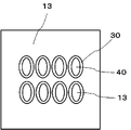
図4において、被覆部30は、帯状の形状である。被覆部30は、所定の幅を有して電極13の上面の配線部9が接合される予定の位置を囲んで予め配置される。被覆部30で囲まれた領域が開口部40である。被覆部30は、電極13の上面に楕円形状で所定の間隔を空けて複数配置されている。被覆部30の楕円形状の内部(開口部40)には、電極13が露出している。開口部40内で露出した電極13の上面には、配線部9が接合される。被覆部30の外周部よりも外側には、電極13が露出している。 In FIG. 4, the covering portion 30 has a belt-like shape. The covering portion 30 has a predetermined width and is arranged in advance so as to surround a position where the wiring portion 9 on the upper surface of the electrode 13 is to be joined. A region surrounded by the covering portion 30 is the opening portion 40 . A plurality of covering portions 30 are arranged on the upper surface of the electrode 13 in an elliptical shape at predetermined intervals. The electrode 13 is exposed in the elliptical interior (opening 40 ) of the cover 30 . The wiring portion 9 is joined to the upper surface of the electrode 13 exposed in the opening portion 40 . The electrode 13 is exposed outside the outer peripheral portion of the covering portion 30 .

図5において、被覆部30の内周部(内側部)よりも内側の開口部40には、配線部9が電極13の上面と接合されている。電極13の上面と配線部9との接合箇所は、接合部31である。接合部31は、被覆部30の内周部と所定の間隔を空けて形成されている。 In FIG. 5, the wiring portion 9 is joined to the upper surface of the electrode 13 in the opening portion 40 inside the inner peripheral portion (inner portion) of the covering portion 30 . A joint portion 31 is a joint portion between the upper surface of the electrode 13 and the wiring portion 9 . The joint portion 31 is formed with a predetermined gap from the inner peripheral portion of the covering portion 30 .

図6は、被覆部30の別の形態を表している。図6において、楕円形状の被覆部30は、複数の被覆部30の一部が重なって(接して)配置されている。この場合においても、それぞれの被覆部30の内周部よりも内側の開口部40には、配線部9が電極13の上面と接合する領域が設けられている。被覆部30の外周部よりも外側には、電極13が露出している。 FIG. 6 shows another form of the covering portion 30. As shown in FIG. In FIG. 6 , the elliptical covering portion 30 is arranged such that a plurality of covering portions 30 are partially overlapped (in contact with each other). Also in this case, the opening 40 inside the inner peripheral portion of each covering portion 30 is provided with a region where the wiring portion 9 is bonded to the upper surface of the electrode 13 . The electrode 13 is exposed outside the outer peripheral portion of the covering portion 30 .

図7において、被覆部30の形状は、電極13の上面よりも面積小さい矩形である。被覆部30は、被覆部30の外縁よりも内側に、楕円形状をした被覆部30の無い領域である開口部40を有している。被覆部30で囲まれた開口部40内では、電極13の上面が露出している。開口部40は、電極13の上面と配線部9とが接合する領域である。被覆部30の外縁形状は、被覆部30の内縁形状が異なっている。 In FIG. 7 , the shape of the covering portion 30 is a rectangle whose area is smaller than the top surface of the electrode 13 . The covering portion 30 has an opening 40 which is an oval-shaped region without the covering portion 30 inside the outer edge of the covering portion 30 . The upper surface of the electrode 13 is exposed within the opening 40 surrounded by the cover 30 . The opening 40 is a region where the upper surface of the electrode 13 and the wiring portion 9 are joined. The inner edge shape of the covering portion 30 is different from the outer edge shape of the covering portion 30 .

図8において、被覆部30は、電極13の外縁まで形成されている。その他の点に関しては、図7に示した被覆部30と同様な形状をしている。被覆部30内には、開口部40が複数設けられている。 In FIG. 8, the covering portion 30 is formed up to the outer edge of the electrode 13 . In other respects, it has the same shape as the covering portion 30 shown in FIG. A plurality of openings 40 are provided in the cover 30 .

図9において、被覆部30は、帯状の形状である。しかしながら、図4とは異なり、被覆部30の内縁(内周部)は、四角形状(矩形)である。被覆部30の内側には開口部40を有している。開口部40では、電極13の上面が露出している。露出した電極13の上面には、配線部9が接合される。この場合、被覆部30の内周部よりも内側には、配線部9が一本または複数本接合される。配線部9の本数は、半導体装置100の仕様(電流密度等)に応じて適宜選択することができる。 In FIG. 9, the covering portion 30 has a belt-like shape. However, unlike FIG. 4, the inner edge (inner peripheral portion) of the covering portion 30 is quadrangular (rectangular). An opening 40 is provided inside the cover 30 . The upper surface of the electrode 13 is exposed at the opening 40 . The wiring part 9 is joined to the exposed upper surface of the electrode 13 . In this case, one or a plurality of wiring portions 9 are joined inside the inner peripheral portion of the covering portion 30 . The number of wiring portions 9 can be appropriately selected according to the specifications (current density, etc.) of the semiconductor device 100 .

図10は、図9の被覆部30の内部に複数の配線部9を接合した状態を示している。図10において、配線部9は、被覆部30の内周部から内側の開口部40に間隔を空けて電極13の上面に接合される。 FIG. 10 shows a state in which a plurality of wiring portions 9 are joined inside the covering portion 30 of FIG. In FIG. 10, the wiring portion 9 is joined to the upper surface of the electrode 13 with a gap from the inner peripheral portion of the covering portion 30 to the inner opening portion 40 .

図12においては、図9に示した帯状の被覆部30の外縁を電極13の外縁と同じ領域まで拡げた形状をしている。被覆部30の内周部よりも内側の開口部40には、図9の場合と同様に配線部9が接合されている。 In FIG. 12, the outer edge of the strip-shaped covering portion 30 shown in FIG. 9 is expanded to the same area as the outer edge of the electrode 13. The wiring portion 9 is joined to the opening portion 40 inside the inner peripheral portion of the covering portion 30 in the same manner as in the case of FIG.

図において、電極13の上面に対する被覆部30の形成面積(割合)が大きくなるほど、電極13の上面における電極13と封止部10との熱応力が緩和でき、封止部10の剥離抑制効果が大きくなり、半導体装置100の信頼性が向上する。 In the figure, the larger the formation area (ratio) of the covering portion 30 to the upper surface of the electrode 13, the more the thermal stress between the electrode 13 and the sealing portion 10 on the upper surface of the electrode 13 can be relaxed, and the effect of suppressing the peeling of the sealing portion 10 is increased. The size increases, and the reliability of the semiconductor device 100 improves.

次に、上述のように構成された本実施の形態1の半導体装置100の製造方法について説明する。 Next, a method for manufacturing the semiconductor device 100 of the first embodiment configured as described above will be described.

はじめに、半導体ウエハ表面の所定の位置に電極13を例えばスパッタリング法で形成する(電極形成工程)。 First, the electrodes 13 are formed at predetermined positions on the surface of the semiconductor wafer by, for example, sputtering (electrode forming step).

次に、電極13上に被覆部30を形成する(被覆部形成工程)。具体的には、被覆部30が、例えば、感光性ポリイミドの場合、後述の方法で形成できる。まず、電極13上に、感光性ポリイミドを、例えば、ディスペンスで適量塗布する。感光性ポリイミドを塗布後スピンコーターにより、電極13上全面に、均一な膜を形成する。その後、形成したい部分のみが開口しているマスクの上から、UV(紫外線)照射を行うことで、マスクの開口部の下の部分に対応するポリイミドが硬化できる。UV照射後、現像、洗浄し、未硬化のポリイミドを除去することで、所定の部分のみ被覆部30が形成できる。被覆部30に囲まれた内側が開口部40である。 Next, the covering portion 30 is formed on the electrode 13 (covering portion forming step). Specifically, when the covering portion 30 is made of, for example, photosensitive polyimide, it can be formed by a method described later. First, an appropriate amount of photosensitive polyimide is applied on the electrode 13 by, for example, dispensing. After applying photosensitive polyimide, a uniform film is formed on the entire surface of the electrode 13 by a spin coater. After that, UV (ultraviolet) irradiation is performed from above the mask having openings only for the portions to be formed, whereby the polyimide corresponding to the portions below the openings of the mask can be cured. After UV irradiation, development, washing, and removal of uncured polyimide can form the covering portion 30 only on a predetermined portion. The inner side surrounded by the covering portion 30 is the opening portion 40 .

次に、前述の半導体ウエハを小片にダイシングして、電極13上に被覆部30が形成された半導体素子7を作製する(半導体素子準備工程)。 Next, the aforementioned semiconductor wafer is diced into small pieces to fabricate semiconductor elements 7 having covering portions 30 formed on the electrodes 13 (semiconductor element preparation step).

次に、上面に金属層21と下面に金属層23とを有する絶縁基板2を準備する(絶縁基板準備工程)。絶縁層22と上面側の金属層21、下面側の金属層23との接合は、ロウ付けなどにより行う。上面側の金属層21には、電気回路が形成されるため、パターン形状が異なることがよくある。このような場合、上面側の金属層21、下面側の金属層23の大きさ、厚みを調整することで、絶縁層22の上下(おもて裏)面間で熱応力の発生を抑えるようにしてもよい。 Next, the insulating substrate 2 having the metal layer 21 on the upper surface and the metal layer 23 on the lower surface is prepared (insulating substrate preparing step). The insulating layer 22, the metal layer 21 on the upper surface side, and the metal layer 23 on the lower surface side are joined by brazing or the like. Since an electric circuit is formed on the metal layer 21 on the upper surface side, the pattern shape is often different. In such a case, by adjusting the size and thickness of the metal layer 21 on the upper surface side and the metal layer 23 on the lower surface side, generation of thermal stress between the upper and lower (front and back) surfaces of the insulating layer 22 can be suppressed. can be

次に、絶縁基板2の上面側の金属層21の所定の位置に、素子接合部8を介して、ダイシングされた半導体素子7を接合する(半導体素子接合工程)。 Next, the diced semiconductor element 7 is bonded to a predetermined position of the metal layer 21 on the upper surface side of the insulating substrate 2 via the element bonding portion 8 (semiconductor element bonding step).

次に、半導体装置100の底面部となるベース板1を準備する(ベース板準備工程)。 Next, the base plate 1 that becomes the bottom surface of the semiconductor device 100 is prepared (base plate preparing step).

次に、ベース板1の上面に絶縁基板2を基板接合部3で接合する(絶縁基板接合工程)。 Next, the insulating substrate 2 is bonded to the upper surface of the base plate 1 at the substrate bonding portion 3 (insulating substrate bonding step).

次に、半導体素子7と絶縁基板2の上面側の金属層21とを配線部9を用いて電気的に接続する(配線材形成工程)。配線部9がワイヤ、リボン、リードの場合、超音波接合法を用いて接合できる。 Next, the semiconductor element 7 and the metal layer 21 on the upper surface side of the insulating substrate 2 are electrically connected using the wiring portion 9 (wiring material forming step). When the wiring part 9 is a wire, a ribbon, or a lead, it can be joined using an ultrasonic joining method.

次に、絶縁基板2と半導体素子7と配線部9と電極端子12の一端側とを封止部10で封止する(封止工程)。 Next, the insulating substrate 2, the semiconductor element 7, the wiring part 9, and the one end side of the electrode terminal 12 are sealed with the sealing part 10 (sealing process).

以上の主要な製造工程を経ることで、図2に示す半導体装置100が製造できる。 Through the main manufacturing steps described above, the semiconductor device 100 shown in FIG. 2 can be manufactured.

以上のように構成された半導体装置100においては、被覆部30が、配線部9と電極13との接合部31の周りに、配線部9と接触させずに電極13上に形成したので、半導体装置100への通電時の封止部10の剥離が抑制でき、半導体装置100の信頼性を向上することができる。また、半導体装置100の寿命を長寿命化ができる。 In the semiconductor device 100 configured as described above, the covering portion 30 is formed on the electrode 13 around the joint portion 31 between the wiring portion 9 and the electrode 13 without contacting the wiring portion 9. The peeling of the sealing portion 10 when the device 100 is energized can be suppressed, and the reliability of the semiconductor device 100 can be improved. Also, the life of the semiconductor device 100 can be extended.

さらに、配線部9と電極13との接合前に、被覆部30を形成したので、被覆部30の形成状態を容易に検査することができ、プロセスコストを低減することが可能となる。 Furthermore, since the covering portion 30 is formed before joining the wiring portion 9 and the electrode 13, the formation state of the covering portion 30 can be easily inspected, and the process cost can be reduced.

実施の形態2.
本実施の形態2においては、実施の形態1で用いた配線部9を電極端子20の一端を延長して配線部として一体とした構造の電極端子20に置き換えた点が異なる。このように、板状形状を有する電極端子20の一端を配線部として用いた場合においても、半導体装置200への通電時の封止部10の剥離を抑制し、半導体装置200の信頼性を向上することができる。なお、その他の点については、実施の形態1と同様であるので、詳しい説明は省略する。
Embodiment 2.
Embodiment 2 differs from Embodiment 1 in that the wiring portion 9 used in Embodiment 1 is replaced with an electrode terminal 20 having a structure in which one end of the electrode terminal 20 is extended and integrated as a wiring portion. Thus, even when one end of the plate-shaped electrode terminal 20 is used as a wiring portion, peeling of the sealing portion 10 when the semiconductor device 200 is energized is suppressed, and the reliability of the semiconductor device 200 is improved. can do. Since other points are the same as those of the first embodiment, detailed description thereof will be omitted.

図12は、実施の形態2における半導体装置を示す平面構造模式図である。図13は、実施の形態2における半導体装置を示す断面構造模式図である。図14は、実施の形態2における半導体装置の配線部の接合部を拡大して示す断面構造模式図である。図において、半導体装置200は、ベース板1と、絶縁基板2と、接合部である素子接合部8と、接合部である基板接合部3と、半導体素子7と、封止部10と、電極13と、端子接合部14と、配線部である電極端子20と、被覆部30と、被覆部30で囲まれた開口部40と、を備えている。なお、図13は、図12の一点鎖線BBにおける断面構造模式図である。 FIG. 12 is a schematic plan view showing the semiconductor device according to the second embodiment. FIG. 13 is a schematic cross-sectional view showing the semiconductor device according to the second embodiment. FIG. 14 is a cross-sectional structural schematic diagram showing an enlarged junction portion of the wiring portion of the semiconductor device according to the second embodiment. In the figure, a semiconductor device 200 includes a base plate 1, an insulating substrate 2, an element bonding portion 8 that is a bonding portion, a substrate bonding portion 3 that is a bonding portion, a semiconductor element 7, a sealing portion 10, and an electrode. 13 , a terminal joint portion 14 , an electrode terminal 20 that is a wiring portion, a covering portion 30 , and an opening portion 40 surrounded by the covering portion 30 . Note that FIG. 13 is a schematic cross-sectional view along the dashed-dotted line BB in FIG. 12 .

図において、半導体装置200は、ベース板1の上面と絶縁基板2の下面とを基板接合部3を用いて接合している。絶縁基板2の上面と半導体素子7の裏面(下面)とを素子接合部8を用いて接合している。絶縁基板2と絶縁基板2の上面に接合された半導体素子7と一端に板状形状を有する電極端子20の一端側とは、封止部10内に封止されている。なお、電極端子20としては、電極13と接合できればよく、リードフレームを用いてもよい。 In the figure, the semiconductor device 200 has the upper surface of the base plate 1 and the lower surface of the insulating substrate 2 joined together using the substrate joining portion 3 . The upper surface of the insulating substrate 2 and the back surface (lower surface) of the semiconductor element 7 are bonded using the element bonding portion 8 . The insulating substrate 2 , the semiconductor element 7 bonded to the upper surface of the insulating substrate 2 , and one end side of the electrode terminal 20 having a plate-like shape at one end are sealed in the sealing portion 10 . Note that the electrode terminal 20 may be a lead frame as long as it can be connected to the electrode 13 .

図12において、封止部10は、点線にて表示し、封止部10に封止されている部材の位置関係がわかるようにしている。半導体装置200の最外周は、ベース板1の周縁部である。ベース板1の周縁部よりも内側には、封止部10が配置されている。封止部10の外縁よりも内側には、絶縁基板2の絶縁層22が配置されている。絶縁基板2の絶縁層22の外縁よりも内側には、絶縁基板2の上面側の金属層21が配置されている。絶縁基板2の上面側の金属層21の外縁よりも内側には、電極13が表面に形成された半導体素子7が配置されている。半導体素子7の電極13の外縁よりも内側には、開口部40を有する被覆部30が配置されている。開口部40は、所定の幅を有する被覆部30に囲まれた領域である。 In FIG. 12, the sealing portion 10 is indicated by a dotted line so that the positional relationship of the members sealed in the sealing portion 10 can be understood. The outermost periphery of the semiconductor device 200 is the periphery of the base plate 1 . A sealing portion 10 is arranged inside the peripheral portion of the base plate 1 . An insulating layer 22 of the insulating substrate 2 is arranged inside the outer edge of the sealing portion 10 . The metal layer 21 on the upper surface side of the insulating substrate 2 is arranged inside the outer edge of the insulating layer 22 of the insulating substrate 2 . A semiconductor element 7 having an electrode 13 formed thereon is arranged inside the outer edge of the metal layer 21 on the upper surface side of the insulating substrate 2 . A covering portion 30 having an opening 40 is arranged inside the outer edge of the electrode 13 of the semiconductor element 7 . The opening 40 is a region surrounded by the covering portion 30 having a predetermined width.

被覆部30の内縁よりも内側には、被覆部30の内縁と間隔を開けて電極端子20の一端が延在しており、電極端子20の一端と電極13とが接合されている。電極端子20は、電極端子20の一端が絶縁基板2を跨いで半導体素子7の上部まで延在して配置され、他端が封止部10から突出(露出)している。また、他の電極端子20は、電極端子20の一端が絶縁基板2を跨いで絶縁基板2の上面側の金属層21の上部まで延在して配置され、他端が封止部10から突出(露出)している。 One end of the electrode terminal 20 extends inside the inner edge of the covering portion 30 with a gap from the inner edge of the covering portion 30 , and the one end of the electrode terminal 20 and the electrode 13 are joined. One end of the electrode terminal 20 extends across the insulating substrate 2 to the top of the semiconductor element 7 , and the other end protrudes (exposes) from the sealing portion 10 . The other electrode terminal 20 is arranged so that one end of the electrode terminal 20 straddles the insulating substrate 2 and extends to the top of the metal layer 21 on the upper surface side of the insulating substrate 2 , and the other end projects from the sealing portion 10 . (exposed).

図13において、ベース板1の上面と絶縁基板2の下面側の金属層23の下面とを基板接合部3を用いて接合している。絶縁基板2の上面側の金属層21の上面と半導体素子7の裏面とを素子接合部8を用いて接合している。右側(第二)の電極端子20の一端は、端子接合部14を介して、半導体素子7の表面(上面)の電極13と電気的に接続している。また、左側(第一)の電極端子20の一端は、端子接合部14を介して、絶縁基板2の上面側の金属層21と電気的に接続している。封止部10は、絶縁基板2の下面側の金属層23と接合していない(露出した)ベース板1の上面と接して、絶縁基板2と絶縁基板2の上面に接合された半導体素子7とを封止している。電極端子20は、それぞれ、一端側が封止部10内に配置され、他端が封止部10の側面から露出(突出)して配置される。 In FIG. 13, the upper surface of the base plate 1 and the lower surface of the metal layer 23 on the lower surface side of the insulating substrate 2 are joined using the substrate joint portion 3 . The upper surface of the metal layer 21 on the upper surface side of the insulating substrate 2 and the back surface of the semiconductor element 7 are bonded using the element bonding portion 8 . One end of the right (second) electrode terminal 20 is electrically connected to the electrode 13 on the surface (upper surface) of the semiconductor element 7 via the terminal joint portion 14 . One end of the left (first) electrode terminal 20 is electrically connected to the metal layer 21 on the upper surface side of the insulating substrate 2 via the terminal joint portion 14 . The sealing portion 10 is in contact with the upper surface of the base plate 1 that is not bonded (exposed) to the metal layer 23 on the lower surface side of the insulating substrate 2 , and the insulating substrate 2 and the semiconductor element 7 bonded to the upper surface of the insulating substrate 2 . and are sealed. Each of the electrode terminals 20 has one end disposed inside the sealing portion 10 and the other end exposed (projecting) from the side surface of the sealing portion 10 .

図14において、半導体素子7の表面に配置された電極13と電極端子20の一端とは、端子接合部14を介して、電極13上の接合部32で接合されている。接合部32は、電極13の上面と端子接合部14の下面との接合箇所である。また、電極端子20の一端側の下面と端子接合部14の上面との接合箇所は接合部33である。被覆部30は、接合部32を囲んでいる。被覆部30で囲まれた領域は、開口部40である。接合部32の外縁(外周部)と被覆部30の内縁(内周部)とは隙間(間隔)Sを空けて配置される。封止部10は、隙間Sの部分では、電極13の表面と接して配置されている。また、封止部10は、隙間Sよりも外側(被覆部30の内縁よりも外側)では、被覆部30の表面と接して配置されている。 In FIG. 14, the electrode 13 arranged on the surface of the semiconductor element 7 and one end of the electrode terminal 20 are joined at the joint portion 32 on the electrode 13 via the terminal joint portion 14 . The joint portion 32 is a joint portion between the upper surface of the electrode 13 and the lower surface of the terminal joint portion 14 . A joint portion 33 is a joint portion between the lower surface of one end of the electrode terminal 20 and the upper surface of the terminal joint portion 14 . The covering portion 30 surrounds the joint portion 32 . A region surrounded by the covering portion 30 is an opening portion 40 . The outer edge (peripheral portion) of the joint portion 32 and the inner edge (inner peripheral portion) of the covering portion 30 are arranged with a gap (interval) S therebetween. The sealing portion 10 is arranged in contact with the surface of the electrode 13 in the gap S portion. Further, the sealing portion 10 is arranged in contact with the surface of the covering portion 30 outside the gap S (outside the inner edge of the covering portion 30).

また、接合部32の外縁と被覆部30の内周部との間隔(距離)は、20μm以上50μm以下である。被覆部30の内周部よりも内側の20μm以上50μm以下の範囲の電極13の表面上である隙間Sに、端子接合部14が濡れ広がるのを防止するための表面処理を行っても良い。表面処理としては、レーザー照射等により局所的に電極13の表面を荒らすことで対応する。この表面処理を行うことで、被覆部30の内周部と端子接合部14とが接触することを抑制でき、表面処理を行った電極13の表面と封止部10とが接することで、封止部10の剥離防止ができる。このように、電極13の被覆部30の内周部よりも内側の領域に表面処理をすることで、端子接合部14の濡れ広がりを防止しながら、封止部10と電極13との密着性を向上させることが可能となる。 Further, the interval (distance) between the outer edge of the joint portion 32 and the inner peripheral portion of the covering portion 30 is 20 μm or more and 50 μm or less. The gap S on the surface of the electrode 13 in the range of 20 μm or more and 50 μm or less inside the inner peripheral portion of the covering portion 30 may be subjected to surface treatment to prevent the terminal joint portion 14 from wetting and spreading. As the surface treatment, the surface of the electrode 13 is locally roughened by laser irradiation or the like. By performing this surface treatment, it is possible to suppress the contact between the inner peripheral portion of the covering portion 30 and the terminal joint portion 14, and the contact between the surface of the electrode 13 subjected to the surface treatment and the sealing portion 10 prevents sealing. The stopper portion 10 can be prevented from peeling off. In this way, by surface-treating the region inside the inner peripheral portion of the covering portion 30 of the electrode 13, the adhesion between the sealing portion 10 and the electrode 13 is improved while preventing the terminal joint portion 14 from wetting and spreading. can be improved.

なお、この表面処理に関しては、電極13の全面に行うと、半導体素子7へのダメージ導入となる可能性がある。しかしながら、本実施の形態のように、半導体素子7の電極13の被覆部30の開口部40の隙間Sのみに表面処理を行うのであれば、半導体素子7に対する割合も少ないのでダメージの影響を考慮しなくてもよい。言い換えると、半導体装置の信頼性に影響を与えない。 Note that if this surface treatment is performed on the entire surface of the electrode 13, there is a possibility that the semiconductor element 7 will be damaged. However, if surface treatment is performed only on the gap S of the opening 40 of the covering portion 30 of the electrode 13 of the semiconductor element 7 as in the present embodiment, the effect of damage should be taken into account because the proportion of the surface treatment to the semiconductor element 7 is small. You don't have to. In other words, it does not affect the reliability of the semiconductor device.

電極端子20は、絶縁基板2の辺部を跨いで配置され、電極端子20の他端は、封止部10から外部へ突出(露出)している。電極端子20の一端は、封止部10の内部に封止されている。右側の電極端子20の一端は、端子接合部14を介して、半導体素子7の表面(上面)の電極13と電気的に接続している。また、左側の電極端子20の一端は、端子接合部14を介して、絶縁基板2の上面側の金属層21の所定の位置と電気的に接続している。封止部10は、絶縁基板2の下面側の金属層23と接合していない(露出した)ベース板1の上面と接して、電極端子20の一端側と絶縁基板2と絶縁基板2の上面に接合された半導体素子7とを封止している。電極端子20としては、銅合金製リード(リードフレーム)を用いることができる。 The electrode terminal 20 is arranged across the side portion of the insulating substrate 2 , and the other end of the electrode terminal 20 protrudes (exposes) from the sealing portion 10 to the outside. One end of the electrode terminal 20 is sealed inside the sealing portion 10 . One end of the electrode terminal 20 on the right side is electrically connected to the electrode 13 on the surface (upper surface) of the semiconductor element 7 via the terminal joint portion 14 . One end of the left electrode terminal 20 is electrically connected to a predetermined position of the metal layer 21 on the upper surface side of the insulating substrate 2 via the terminal joint portion 14 . The sealing portion 10 is in contact with the upper surface of the base plate 1 that is not joined (exposed) to the metal layer 23 on the lower surface side of the insulating substrate 2 , and the one end side of the electrode terminal 20 , the insulating substrate 2 , and the upper surface of the insulating substrate 2 . It seals the semiconductor element 7 joined to the . A copper alloy lead (lead frame) can be used as the electrode terminal 20 .

端子接合部14は、電極13の上面と電極端子20の一端側とを接合するための接合材である。端子接合部14の材料としては、基板接合部3と同様に、はんだ、焼結銀または焼結銅などを用いることができる。 The terminal joint portion 14 is a joint material for joining the upper surface of the electrode 13 and one end side of the electrode terminal 20 . Solder, sintered silver, sintered copper, or the like can be used as the material of the terminal joint portion 14, similarly to the board joint portion 3. FIG.

以上のように構成された半導体装置200においては、被覆部30が、電極端子20の一端と電極13との接合部32の周りに、電極端子20の一端と接触させずに電極13上に形成したので、半導体装置200への通電時の封止部10の剥離が抑制でき、半導体装置200の信頼性を向上することができる。また、半導体装置200の寿命を長寿命化ができる。 In the semiconductor device 200 configured as described above, the covering portion 30 is formed on the electrode 13 around the joint portion 32 between the one end of the electrode terminal 20 and the electrode 13 without contacting the one end of the electrode terminal 20 . Therefore, peeling of the sealing portion 10 when the semiconductor device 200 is energized can be suppressed, and the reliability of the semiconductor device 200 can be improved. Also, the life of the semiconductor device 200 can be extended.

さらに、電極端子20の一端と電極13との接合前に、被覆部30を形成したので、被覆部30の形成状態を容易に検査することができ、プロセスコストを低減することが可能となる。 Furthermore, since the covering portion 30 is formed before the one end of the electrode terminal 20 and the electrode 13 are joined, the formation state of the covering portion 30 can be easily inspected, and the process cost can be reduced.

実施の形態3.
本実施の形態3は、上述した実施の形態1から2にかかる半導体装置を電力変換装置に適用したものである。本開示は特定の電力変換装置に限定されるものではないが、以下、実施の形態3として、三相のインバータに本開示を適用した場合について説明する。
Embodiment 3.
The third embodiment applies the semiconductor devices according to the first and second embodiments described above to a power converter. Although the present disclosure is not limited to a specific power converter, a case where the present disclosure is applied to a three-phase inverter will be described below as a third embodiment.

図15は、本開示の実施の形態3における電力変換装置を適用した電力変換システムの構成を示すブロック図である。 FIG. 15 is a block diagram showing a configuration of a power conversion system to which a power conversion device according to Embodiment 3 of the present disclosure is applied.

図15に示す電力変換システムは、電源1000、電力変換装置2000、負荷3000を備えている。電源1000は、直流電源であり、電力変換装置2000に直流電力を供給する。電源1000は種々のもので構成することができ、例えば、直流系統、太陽電池、蓄電池で構成することができるし、交流系統に接続された整流回路、AC/DCコンバータなどで構成することとしてもよい。また、電源1000を、直流系統から出力される直流電力を所定の電力に変換するDC/DCコンバータによって構成することとしてもよい。 The power conversion system shown in FIG. 15 includes a power supply 1000, a power conversion device 2000, and a load 3000. The power supply 1000 is a DC power supply and supplies DC power to the power converter 2000 . The power supply 1000 can be composed of various things, for example, it can be composed of a DC system, a solar battery, a storage battery, or it can be composed of a rectifier circuit connected to an AC system, an AC/DC converter, etc. good. Also, power supply 1000 may be configured by a DC/DC converter that converts DC power output from a DC system into predetermined power.

電力変換装置2000は、電源1000と負荷3000との間に接続された三相のインバータであり、電源1000から供給された直流電力を交流電力に変換し、負荷3000に交流電力を供給する。電力変換装置2000は、図15に示すように、電源1000から入力される直流電力を交流電力に変換して出力する主変換回路2001と、主変換回路2001を制御する制御信号を主変換回路2001に出力する制御回路2003とを備えている。 Power converter 2000 is a three-phase inverter connected between power supply 1000 and load 3000 , converts DC power supplied from power supply 1000 into AC power, and supplies AC power to load 3000 . As shown in FIG. 15, the power conversion device 2000 includes a main conversion circuit 2001 that converts DC power input from a power source 1000 into AC power and outputs the same, and a control signal that controls the main conversion circuit 2001 to the main conversion circuit 2001. and a control circuit 2003 for outputting to.

負荷3000は、電力変換装置2000から供給された交流電力によって駆動される三相の電動機である。なお、負荷3000は特定の用途に限られるものではなく、各種電気機器に搭載された電動機であり、例えば、ハイブリッド自動車、電気自動車、鉄道車両、エレベーター、空調機器向けの電動機等として用いられる。 Load 3000 is a three-phase electric motor driven by AC power supplied from power conversion device 2000 . It should be noted that the load 3000 is not limited to a specific application, but is an electric motor mounted on various electrical equipment, such as hybrid automobiles, electric automobiles, railroad cars, elevators, and electric motors for air conditioners.

以下、電力変換装置2000の詳細を説明する。主変換回路2001は、半導体装置2002に内蔵されたスイッチング素子と還流ダイオードとを備えており(図示せず)、スイッチング素子がスイッチングすることによって、電源1000から供給される直流電力を交流電力に変換し、負荷3000に供給する。主変換回路2001の具体的な回路構成は種々のものがあるが、本実施の形態にかかる主変換回路2001は2レベルの三相フルブリッジ回路であり、6つのスイッチング素子とそれぞれのスイッチング素子に逆並列に接続された6つの還流ダイオードとから構成することができる。主変換回路2001は、各スイッチング素子、各還流ダイオードなどを内蔵する上述した実施の形態1から5のいずれかに相当する半導体装置2002によって構成される。6つのスイッチング素子は2つのスイッチング素子ごとに直列接続され上下アームを構成し、各上下アームはフルブリッジ回路の各相(U相、V相、W相)を構成する。各上下アームの出力端子、すなわち主変換回路2001の3つの出力端子は、負荷3000に接続される。 Details of the power converter 2000 will be described below. The main conversion circuit 2001 includes a switching element and a freewheeling diode (not shown) built in the semiconductor device 2002. By switching the switching element, the DC power supplied from the power supply 1000 is converted into AC power. and supply it to the load 3000 . Although the main conversion circuit 2001 has various specific circuit configurations, the main conversion circuit 2001 according to the present embodiment is a two-level three-phase full bridge circuit, and has six switching elements and It can be composed of six freewheeling diodes connected in anti-parallel. The main conversion circuit 2001 is configured by a semiconductor device 2002 corresponding to any one of the above-described first to fifth embodiments, which incorporates switching elements, freewheeling diodes, and the like. Six switching elements are connected in series every two switching elements to form upper and lower arms, and each upper and lower arm forms each phase (U phase, V phase, W phase) of the full bridge circuit. The output terminals of each upper and lower arm, that is, the three output terminals of main conversion circuit 2001 are connected to load 3000 .

また、主変換回路2001は、各スイッチング素子を駆動する駆動回路(図示なし)を備えている。駆動回路は半導体装置2002に内蔵されていてもよいし、半導体装置2002とは別に駆動回路を備える構成であってもよい。駆動回路は、主変換回路2001のスイッチング素子を駆動する駆動信号を生成し、主変換回路2001のスイッチング素子の制御電極に供給する。具体的には、後述する制御回路2003からの制御信号に従い、スイッチング素子をオン状態にする駆動信号とスイッチング素子をオフ状態にする駆動信号とを各スイッチング素子の制御電極に出力する。スイッチング素子をオン状態に維持する場合、駆動信号はスイッチング素子の閾値電圧以上の電圧信号(オン信号)であり、スイッチング素子をオフ状態に維持する場合、駆動信号はスイッチング素子の閾値電圧以下の電圧信号(オフ信号)となる。 The main conversion circuit 2001 also includes a drive circuit (not shown) that drives each switching element. The driver circuit may be built in the semiconductor device 2002, or may be configured to include a driver circuit separately from the semiconductor device 2002. FIG. The drive circuit generates a drive signal for driving the switching element of the main conversion circuit 2001 and supplies it to the control electrode of the switching element of the main conversion circuit 2001 . Specifically, in accordance with a control signal from the control circuit 2003, which will be described later, a drive signal for turning on the switching element and a drive signal for turning off the switching element are output to the control electrode of each switching element. When maintaining the switching element in the ON state, the driving signal is a voltage signal (ON signal) equal to or higher than the threshold voltage of the switching element, and when maintaining the switching element in the OFF state, the driving signal is a voltage equal to or less than the threshold voltage of the switching element. signal (off signal).

制御回路2003は、負荷3000に所望の電力が供給されるよう主変換回路2001のスイッチング素子を制御する。具体的には、負荷3000に供給すべき電力に基づいて主変換回路2001の各スイッチング素子がオン状態となるべき時間(オン時間)を算出する。例えば、出力すべき電圧に応じてスイッチング素子のオン時間を変調するPWM制御によって主変換回路2001を制御することができる。また、各時点においてオン状態となるべきスイッチング素子にはオン信号を出力し、オフ状態となるべきスイッチング素子にはオフ信号を出力されるように、主変換回路2001が備える駆動回路に制御指令(制御信号)を出力する。駆動回路は、この制御信号に従い、各スイッチング素子の制御電極にオン信号又はオフ信号を駆動信号として出力する。 Control circuit 2003 controls switching elements of main converter circuit 2001 so that desired power is supplied to load 3000 . Specifically, based on the power to be supplied to the load 3000, the time (on time) during which each switching element of the main converter circuit 2001 should be in the ON state is calculated. For example, the main conversion circuit 2001 can be controlled by PWM control that modulates the ON time of the switching element according to the voltage to be output. Further, a control command ( control signal). The drive circuit outputs an ON signal or an OFF signal as a drive signal to the control electrode of each switching element according to this control signal.

以上のように構成された本実施の形態5に係る電力変換装置においては、主変換回路2001の半導体装置2002として実施の形態1から4にかかる半導体装置を適用するため、信頼性向上を実現することができる。 In the power conversion device according to the fifth embodiment configured as described above, since the semiconductor device according to the first to fourth embodiments is applied as the semiconductor device 2002 of the main conversion circuit 2001, the reliability is improved. be able to.

本実施の形態では、2レベルの三相インバータに本開示を適用する例を説明したが、本開示は、これに限られるものではなく、種々の電力変換装置に適用することができる。本実施の形態では、2レベルの電力変換装置としたが3レベル、マルチレベルの電力変換装置であってもよいし、単相負荷に電力を供給する場合には単相のインバータに本開示を適用してもよい。また、直流負荷等に電力を供給する場合にはDC/DCコンバータ、AC/DCコンバータなどに本開示を適用することもできる。 In the present embodiment, an example in which the present disclosure is applied to a two-level three-phase inverter has been described, but the present disclosure is not limited to this, and can be applied to various power converters. In this embodiment, a two-level power conversion device is used, but a three-level or multi-level power conversion device may also be used. may apply. In addition, the present disclosure can be applied to DC/DC converters, AC/DC converters, etc. when power is supplied to a DC load or the like.

また、本開示を適用した電力変換装置は、上述した負荷が電動機の場合に限定されるものではなく、例えば、放電加工機、レーザー加工機、誘導加熱調理器、非接触器給電システムの電源装置等として用いることもでき、さらには、太陽光発電システム、蓄電システム等のパワーコンディショナーとして用いることもできる。 In addition, the power conversion device to which the present disclosure is applied is not limited to the case where the above-described load is an electric motor. etc., and furthermore, it can be used as a power conditioner for a photovoltaic power generation system, an electric storage system, and the like.

特に、半導体素子7として、SiCを用いた場合、電力用半導体素子はその特徴を生かすために、Siの時と比較してより高温で動作させることになる。SiCデバイスを搭載する半導体装置においては、より高い信頼性が求められるため、高信頼の半導体装置を実現するという本開示のメリットはより効果的なものとなる。 In particular, when SiC is used as the semiconductor element 7, the power semiconductor element is operated at a higher temperature than when Si is used in order to take advantage of its characteristics. Since higher reliability is required for semiconductor devices on which SiC devices are mounted, the advantage of the present disclosure that a highly reliable semiconductor device is realized becomes more effective.

上述した実施の形態は、すべての点で例示であって制限的なものではないと解されるべきである。本開示の範囲は、上述した実施形態の範囲ではなく、特許請求の範囲によって示され、特許請求の範囲と均等の意味及び範囲内でのすべての変更を含むものである。また、上記の実施形態に開示されている複数の構成要素を適宜組み合わせることにより発明を形成してもよい。 It should be understood that the above-described embodiments are illustrative in all respects and not restrictive. The scope of the present disclosure is indicated by the scope of claims rather than the scope of the above-described embodiments, and includes all modifications within the scope and meaning equivalent to the scope of claims. Also, the invention may be formed by appropriately combining a plurality of constituent elements disclosed in the above embodiments.

1 ベース板、2 絶縁基板、3 基板接合部、7 半導体素子、8 素子接合部、9 配線部、10 封止部、12,20 電極端子、13 電極、14 端子接合部、30 被覆部、31,32,33 接合部、100,200,300,400,500,600,2002 半導体装置、1000 電源、2000 電力変換装置、2001 主変換回路、2003 制御回路、3000 負荷。 Reference Signs List 1 base plate 2 insulating substrate 3 substrate joint portion 7 semiconductor element 8 element joint portion 9 wiring portion 10 sealing portion 12, 20 electrode terminal 13 electrode 14 terminal joint portion 30 covering portion 31 , 32, 33 junction, 100, 200, 300, 400, 500, 600, 2002 semiconductor device, 1000 power source, 2000 power converter, 2001 main conversion circuit, 2003 control circuit, 3000 load.

Claims (8)

上面に電極を有する半導体素子と、
開口部を有して前記電極の表面を被覆する被覆部と、
前記被覆部の前記開口部の内周部と間隔を空けて前記開口部内に配置されたワイヤである配線部と、
前記被覆部と前記配線部と前記半導体素子とを封止する封止部と、
を備え、
前記開口部は、前記電極と前記配線部との接合部の周囲に前記電極が前記被覆部で被覆されないよう隙間を開けるように配置されることを特徴とする半導体装置。
a semiconductor element having an electrode on its upper surface;
a covering portion that has an opening and covers the surface of the electrode;
a wiring portion that is a wire arranged in the opening with a gap from the inner peripheral portion of the opening of the covering portion;
a sealing portion that seals the covering portion, the wiring portion, and the semiconductor element;
with
The semiconductor device according to claim 1, wherein the opening is arranged around a joint portion between the electrode and the wiring portion so as to form a gap so that the electrode is not covered with the covering portion .
前記被覆部の弾性率は、前記封止部の弾性率と比べて低い、請求項1に記載の半導体装置。 2. The semiconductor device according to claim 1, wherein an elastic modulus of said covering portion is lower than an elastic modulus of said sealing portion. 前記被覆部と前記封止部との接着強度は、前記電極と前記封止部との接着強度と比べて高い、請求項1または請求項2に記載の半導体装置。 3. The semiconductor device according to claim 1, wherein adhesive strength between said covering portion and said sealing portion is higher than adhesive strength between said electrode and said sealing portion. 前記被覆部は、複数の前記開口部を有している、請求項1から請求項3のいずれか1項に記載の半導体装置。 4. The semiconductor device according to claim 1, wherein said covering portion has a plurality of said openings. 前記開口部には、複数の前記配線部が配置されている、請求項1から請求項3のいずれか1項に記載の半導体装置。 4. The semiconductor device according to claim 1, wherein a plurality of said wiring portions are arranged in said opening. 前記配線部と前記被覆部の内周部との間隔は、20μm以上50μm以下である、請求項1から請求項5のいずれか1項に記載の半導体装置。 6. The semiconductor device according to claim 1, wherein a distance between said wiring portion and an inner peripheral portion of said covering portion is 20 [mu]m or more and 50 [mu]m or less. 前記配線部は、リードフレームである、請求項1から請求項6のいずれか1項に記載の半導体装置。 7. The semiconductor device according to claim 1, wherein said wiring portion is a lead frame. 請求項1から請求項のいずれか1項に記載の半導体装置を有し、入力される電力を変換して出力する主変換回路と、
前記主変換回路を制御する制御信号を前記主変換回路に出力する制御回路と、
を備えた、電力変換装置。
A main conversion circuit that has the semiconductor device according to any one of claims 1 to 7 and that converts and outputs input power;
a control circuit that outputs a control signal for controlling the main conversion circuit to the main conversion circuit;
A power conversion device comprising:
JP2022518732A 2021-11-04 2021-11-04 Semiconductor equipment and power conversion equipment Active JP7176662B1 (en)

Applications Claiming Priority (1)

Application Number Priority Date Filing Date Title
PCT/JP2021/040622 WO2023079640A1 (en) 2021-11-04 2021-11-04 Semiconductor device and power conversion apparatus

Publications (3)

Publication Number Publication Date
JP7176662B1 true JP7176662B1 (en) 2022-11-22
JPWO2023079640A1 JPWO2023079640A1 (en) 2023-05-11
JPWO2023079640A5 JPWO2023079640A5 (en) 2023-10-03

Family

ID=84144809

Family Applications (1)

Application Number Title Priority Date Filing Date
JP2022518732A Active JP7176662B1 (en) 2021-11-04 2021-11-04 Semiconductor equipment and power conversion equipment

Country Status (2)

Country Link
JP (1) JP7176662B1 (en)
WO (1) WO2023079640A1 (en)

Citations (6)

* Cited by examiner, † Cited by third party
Publication number Priority date Publication date Assignee Title
JPH0982851A (en) * 1995-09-13 1997-03-28 Matsushita Electron Corp Semiconductor device
JPH11186319A (en) * 1997-12-19 1999-07-09 Matsushita Electron Corp Semiconductor device and manufacture thereof
JP2006165515A (en) * 2004-11-11 2006-06-22 Denso Corp Semiconductor device and its manufacturing method
JP2008294219A (en) * 2007-05-24 2008-12-04 Toshiba Corp Semiconductor device, and manufacturing method thereof
JP2016028417A (en) * 2014-07-11 2016-02-25 ローム株式会社 Electronic device
JP2020043154A (en) * 2018-09-07 2020-03-19 三菱電機株式会社 Semiconductor device and manufacturing method therefor, and power conversion device

Patent Citations (6)

* Cited by examiner, † Cited by third party
Publication number Priority date Publication date Assignee Title
JPH0982851A (en) * 1995-09-13 1997-03-28 Matsushita Electron Corp Semiconductor device
JPH11186319A (en) * 1997-12-19 1999-07-09 Matsushita Electron Corp Semiconductor device and manufacture thereof
JP2006165515A (en) * 2004-11-11 2006-06-22 Denso Corp Semiconductor device and its manufacturing method
JP2008294219A (en) * 2007-05-24 2008-12-04 Toshiba Corp Semiconductor device, and manufacturing method thereof
JP2016028417A (en) * 2014-07-11 2016-02-25 ローム株式会社 Electronic device
JP2020043154A (en) * 2018-09-07 2020-03-19 三菱電機株式会社 Semiconductor device and manufacturing method therefor, and power conversion device

Also Published As

Publication number Publication date
JPWO2023079640A1 (en) 2023-05-11
WO2023079640A1 (en) 2023-05-11

Similar Documents

Publication Publication Date Title
JP6399272B1 (en) Power module, manufacturing method thereof, and power conversion device
JP6806170B2 (en) Semiconductor equipment and power conversion equipment
JP6826665B2 (en) Semiconductor devices, manufacturing methods for semiconductor devices, and power conversion devices
WO2019049400A1 (en) Power module, production method therefor, and power conversion device
JP6575739B1 (en) Semiconductor device, semiconductor device manufacturing method, and power conversion device
US20220415747A1 (en) Power module and power conversion device
JP7176662B1 (en) Semiconductor equipment and power conversion equipment
JP7134345B2 (en) SEMICONDUCTOR MODULE, SEMICONDUCTOR MODULE MANUFACTURING METHOD AND POWER CONVERTER
JP6885522B1 (en) Semiconductor device, power conversion device and manufacturing method of semiconductor device
WO2020148879A1 (en) Semiconductor device, production method for semiconductor device, and power conversion device
JP7088421B1 (en) Semiconductor devices and power converters
US11887903B2 (en) Power semiconductor device, method for manufacturing power semiconductor device, and power conversion apparatus
JP6680419B1 (en) SEMICONDUCTOR DEVICE, SEMICONDUCTOR DEVICE MANUFACTURING METHOD, AND POWER CONVERSION DEVICE
JP7270772B2 (en) Semiconductor device, power conversion device, and method for manufacturing semiconductor device
WO2022239154A1 (en) Power module and power converting device
JP7106007B2 (en) Semiconductor equipment and power conversion equipment
JP7438466B1 (en) Semiconductor device and its manufacturing method, and power conversion device
JP7237192B2 (en) Semiconductor device, manufacturing method thereof, and power conversion device
WO2024090278A1 (en) Semiconductor device, power conversion device, and semiconductor device production method
JP7334369B1 (en) Power module and power converter
JP7229382B2 (en) Semiconductor device, power conversion device, and method for manufacturing semiconductor device
JP7132340B2 (en) Semiconductor equipment and power conversion equipment
JP7019024B2 (en) Semiconductor equipment and power conversion equipment
WO2019171666A1 (en) Semiconductor device, electric power converter and method for producing semiconductor device
JP2023013642A (en) Semiconductor device

Legal Events

Date Code Title Description
A521 Request for written amendment filed

Free format text: JAPANESE INTERMEDIATE CODE: A523

Effective date: 20220323

A621 Written request for application examination

Free format text: JAPANESE INTERMEDIATE CODE: A621

Effective date: 20220323

A871 Explanation of circumstances concerning accelerated examination

Free format text: JAPANESE INTERMEDIATE CODE: A871

Effective date: 20220323

RD01 Notification of change of attorney

Free format text: JAPANESE INTERMEDIATE CODE: A7421

Effective date: 20220427

A131 Notification of reasons for refusal

Free format text: JAPANESE INTERMEDIATE CODE: A131

Effective date: 20220621

A521 Request for written amendment filed

Free format text: JAPANESE INTERMEDIATE CODE: A523

Effective date: 20220819

TRDD Decision of grant or rejection written
A01 Written decision to grant a patent or to grant a registration (utility model)

Free format text: JAPANESE INTERMEDIATE CODE: A01

Effective date: 20221011

A61 First payment of annual fees (during grant procedure)

Free format text: JAPANESE INTERMEDIATE CODE: A61

Effective date: 20221024

R151 Written notification of patent or utility model registration

Ref document number: 7176662

Country of ref document: JP

Free format text: JAPANESE INTERMEDIATE CODE: R151