JP7150461B2 - semiconductor equipment - Google Patents
semiconductor equipment Download PDFInfo
- Publication number
- JP7150461B2 JP7150461B2 JP2018082981A JP2018082981A JP7150461B2 JP 7150461 B2 JP7150461 B2 JP 7150461B2 JP 2018082981 A JP2018082981 A JP 2018082981A JP 2018082981 A JP2018082981 A JP 2018082981A JP 7150461 B2 JP7150461 B2 JP 7150461B2
- Authority
- JP
- Japan
- Prior art keywords
- semiconductor device
- electrode
- pad
- resin
- main surface
- Prior art date
- Legal status (The legal status is an assumption and is not a legal conclusion. Google has not performed a legal analysis and makes no representation as to the accuracy of the status listed.)
- Active
Links
Images


Classifications
-
- H—ELECTRICITY
- H01—ELECTRIC ELEMENTS
- H01L—SEMICONDUCTOR DEVICES NOT COVERED BY CLASS H10
- H01L23/00—Details of semiconductor or other solid state devices
- H01L23/48—Arrangements for conducting electric current to or from the solid state body in operation, e.g. leads, terminal arrangements ; Selection of materials therefor
- H01L23/488—Arrangements for conducting electric current to or from the solid state body in operation, e.g. leads, terminal arrangements ; Selection of materials therefor consisting of soldered or bonded constructions
- H01L23/495—Lead-frames or other flat leads
- H01L23/49541—Geometry of the lead-frame
- H01L23/49548—Cross section geometry
- H01L23/49551—Cross section geometry characterised by bent parts
- H01L23/49555—Cross section geometry characterised by bent parts the bent parts being the outer leads
-
- H—ELECTRICITY
- H01—ELECTRIC ELEMENTS
- H01L—SEMICONDUCTOR DEVICES NOT COVERED BY CLASS H10
- H01L23/00—Details of semiconductor or other solid state devices
- H01L23/48—Arrangements for conducting electric current to or from the solid state body in operation, e.g. leads, terminal arrangements ; Selection of materials therefor
- H01L23/488—Arrangements for conducting electric current to or from the solid state body in operation, e.g. leads, terminal arrangements ; Selection of materials therefor consisting of soldered or bonded constructions
- H01L23/495—Lead-frames or other flat leads
- H01L23/49503—Lead-frames or other flat leads characterised by the die pad
-
- H—ELECTRICITY
- H01—ELECTRIC ELEMENTS
- H01L—SEMICONDUCTOR DEVICES NOT COVERED BY CLASS H10
- H01L23/00—Details of semiconductor or other solid state devices
- H01L23/48—Arrangements for conducting electric current to or from the solid state body in operation, e.g. leads, terminal arrangements ; Selection of materials therefor
- H01L23/488—Arrangements for conducting electric current to or from the solid state body in operation, e.g. leads, terminal arrangements ; Selection of materials therefor consisting of soldered or bonded constructions
- H01L23/495—Lead-frames or other flat leads
- H01L23/49517—Additional leads
- H01L23/49524—Additional leads the additional leads being a tape carrier or flat leads
-
- H—ELECTRICITY
- H01—ELECTRIC ELEMENTS
- H01L—SEMICONDUCTOR DEVICES NOT COVERED BY CLASS H10
- H01L23/00—Details of semiconductor or other solid state devices
- H01L23/48—Arrangements for conducting electric current to or from the solid state body in operation, e.g. leads, terminal arrangements ; Selection of materials therefor
- H01L23/488—Arrangements for conducting electric current to or from the solid state body in operation, e.g. leads, terminal arrangements ; Selection of materials therefor consisting of soldered or bonded constructions
- H01L23/495—Lead-frames or other flat leads
- H01L23/49537—Plurality of lead frames mounted in one device
-
- H—ELECTRICITY
- H01—ELECTRIC ELEMENTS
- H01L—SEMICONDUCTOR DEVICES NOT COVERED BY CLASS H10
- H01L23/00—Details of semiconductor or other solid state devices
- H01L23/48—Arrangements for conducting electric current to or from the solid state body in operation, e.g. leads, terminal arrangements ; Selection of materials therefor
- H01L23/488—Arrangements for conducting electric current to or from the solid state body in operation, e.g. leads, terminal arrangements ; Selection of materials therefor consisting of soldered or bonded constructions
- H01L23/495—Lead-frames or other flat leads
- H01L23/49541—Geometry of the lead-frame
- H01L23/49562—Geometry of the lead-frame for devices being provided for in H01L29/00
-
- H—ELECTRICITY
- H01—ELECTRIC ELEMENTS
- H01L—SEMICONDUCTOR DEVICES NOT COVERED BY CLASS H10
- H01L2224/00—Indexing scheme for arrangements for connecting or disconnecting semiconductor or solid-state bodies and methods related thereto as covered by H01L24/00
- H01L2224/01—Means for bonding being attached to, or being formed on, the surface to be connected, e.g. chip-to-package, die-attach, "first-level" interconnects; Manufacturing methods related thereto
- H01L2224/02—Bonding areas; Manufacturing methods related thereto
- H01L2224/04—Structure, shape, material or disposition of the bonding areas prior to the connecting process
- H01L2224/06—Structure, shape, material or disposition of the bonding areas prior to the connecting process of a plurality of bonding areas
- H01L2224/0601—Structure
- H01L2224/0603—Bonding areas having different sizes, e.g. different heights or widths
-
- H—ELECTRICITY
- H01—ELECTRIC ELEMENTS
- H01L—SEMICONDUCTOR DEVICES NOT COVERED BY CLASS H10
- H01L2224/00—Indexing scheme for arrangements for connecting or disconnecting semiconductor or solid-state bodies and methods related thereto as covered by H01L24/00
- H01L2224/01—Means for bonding being attached to, or being formed on, the surface to be connected, e.g. chip-to-package, die-attach, "first-level" interconnects; Manufacturing methods related thereto
- H01L2224/02—Bonding areas; Manufacturing methods related thereto
- H01L2224/04—Structure, shape, material or disposition of the bonding areas prior to the connecting process
- H01L2224/06—Structure, shape, material or disposition of the bonding areas prior to the connecting process of a plurality of bonding areas
- H01L2224/061—Disposition
- H01L2224/0618—Disposition being disposed on at least two different sides of the body, e.g. dual array
- H01L2224/06181—On opposite sides of the body
-
- H—ELECTRICITY
- H01—ELECTRIC ELEMENTS
- H01L—SEMICONDUCTOR DEVICES NOT COVERED BY CLASS H10
- H01L2224/00—Indexing scheme for arrangements for connecting or disconnecting semiconductor or solid-state bodies and methods related thereto as covered by H01L24/00
- H01L2224/01—Means for bonding being attached to, or being formed on, the surface to be connected, e.g. chip-to-package, die-attach, "first-level" interconnects; Manufacturing methods related thereto
- H01L2224/26—Layer connectors, e.g. plate connectors, solder or adhesive layers; Manufacturing methods related thereto
- H01L2224/31—Structure, shape, material or disposition of the layer connectors after the connecting process
- H01L2224/32—Structure, shape, material or disposition of the layer connectors after the connecting process of an individual layer connector
- H01L2224/321—Disposition
- H01L2224/32151—Disposition the layer connector connecting between a semiconductor or solid-state body and an item not being a semiconductor or solid-state body, e.g. chip-to-substrate, chip-to-passive
- H01L2224/32221—Disposition the layer connector connecting between a semiconductor or solid-state body and an item not being a semiconductor or solid-state body, e.g. chip-to-substrate, chip-to-passive the body and the item being stacked
- H01L2224/32245—Disposition the layer connector connecting between a semiconductor or solid-state body and an item not being a semiconductor or solid-state body, e.g. chip-to-substrate, chip-to-passive the body and the item being stacked the item being metallic
-
- H—ELECTRICITY
- H01—ELECTRIC ELEMENTS
- H01L—SEMICONDUCTOR DEVICES NOT COVERED BY CLASS H10
- H01L2224/00—Indexing scheme for arrangements for connecting or disconnecting semiconductor or solid-state bodies and methods related thereto as covered by H01L24/00
- H01L2224/01—Means for bonding being attached to, or being formed on, the surface to be connected, e.g. chip-to-package, die-attach, "first-level" interconnects; Manufacturing methods related thereto
- H01L2224/34—Strap connectors, e.g. copper straps for grounding power devices; Manufacturing methods related thereto
- H01L2224/39—Structure, shape, material or disposition of the strap connectors after the connecting process
- H01L2224/40—Structure, shape, material or disposition of the strap connectors after the connecting process of an individual strap connector
- H01L2224/401—Disposition
- H01L2224/40151—Connecting between a semiconductor or solid-state body and an item not being a semiconductor or solid-state body, e.g. chip-to-substrate, chip-to-passive
- H01L2224/40221—Connecting between a semiconductor or solid-state body and an item not being a semiconductor or solid-state body, e.g. chip-to-substrate, chip-to-passive the body and the item being stacked
- H01L2224/40245—Connecting between a semiconductor or solid-state body and an item not being a semiconductor or solid-state body, e.g. chip-to-substrate, chip-to-passive the body and the item being stacked the item being metallic
-
- H—ELECTRICITY
- H01—ELECTRIC ELEMENTS
- H01L—SEMICONDUCTOR DEVICES NOT COVERED BY CLASS H10
- H01L23/00—Details of semiconductor or other solid state devices
- H01L23/28—Encapsulations, e.g. encapsulating layers, coatings, e.g. for protection
- H01L23/31—Encapsulations, e.g. encapsulating layers, coatings, e.g. for protection characterised by the arrangement or shape
- H01L23/3107—Encapsulations, e.g. encapsulating layers, coatings, e.g. for protection characterised by the arrangement or shape the device being completely enclosed
-
- H—ELECTRICITY
- H01—ELECTRIC ELEMENTS
- H01L—SEMICONDUCTOR DEVICES NOT COVERED BY CLASS H10
- H01L23/00—Details of semiconductor or other solid state devices
- H01L23/48—Arrangements for conducting electric current to or from the solid state body in operation, e.g. leads, terminal arrangements ; Selection of materials therefor
- H01L23/488—Arrangements for conducting electric current to or from the solid state body in operation, e.g. leads, terminal arrangements ; Selection of materials therefor consisting of soldered or bonded constructions
- H01L23/495—Lead-frames or other flat leads
- H01L23/49503—Lead-frames or other flat leads characterised by the die pad
- H01L23/49513—Lead-frames or other flat leads characterised by the die pad having bonding material between chip and die pad
-
- H—ELECTRICITY
- H01—ELECTRIC ELEMENTS
- H01L—SEMICONDUCTOR DEVICES NOT COVERED BY CLASS H10
- H01L2924/00—Indexing scheme for arrangements or methods for connecting or disconnecting semiconductor or solid-state bodies as covered by H01L24/00
- H01L2924/15—Details of package parts other than the semiconductor or other solid state devices to be connected
- H01L2924/181—Encapsulation
Description
本開示は、半導体素子を備えた半導体装置に関する。 The present disclosure relates to a semiconductor device having a semiconductor element.
半導体装置は、様々な構成が提案されている。特許文献1には、従来の半導体装置の一例が開示されている。同文献に開示された半導体装置は、半導体素子、複数のリード、導電性金属板(以下、「ストラップ部材」という。)および封止樹脂を備えている。半導体素子は、複数のリードのそれぞれと導通しており、当該複数のリードのいずれかに、ストラップ部材を介して導通している。当該ストラップ部材は、半導体素子の上面に形成された電極の略全面を覆うように接合されている。封止樹脂は、半導体素子、複数のリードの一部ずつ、および、ストラップ部材を覆っている。
Various configurations of semiconductor devices have been proposed.
従来の半導体装置において、ストラップ部材と半導体素子との熱膨張係数が必ずしも等しくない。そのため、ストラップ部材と半導体素子とが接合された領域において、これらの熱膨張係数の差に起因する熱応力が生じ、半導体素子が破損しうる。したがって、半導体装置の信頼性の低下が懸念される。 In a conventional semiconductor device, the thermal expansion coefficients of the strap member and the semiconductor element are not necessarily the same. Therefore, in the region where the strap member and the semiconductor element are joined, thermal stress is generated due to the difference in thermal expansion coefficient between them, and the semiconductor element may be damaged. Therefore, there is a concern that the reliability of the semiconductor device may be lowered.
本開示は、上記課題に鑑みて創作されたものであり、その目的は、信頼性の向上を図った半導体装置を提供することにある。 The present disclosure has been made in view of the above problems, and an object thereof is to provide a semiconductor device with improved reliability.
本開示の第1の側面によって提供される半導体装置は、厚さ方向において互いに反対側を向く素子主面および素子裏面を有し、前記素子主面に第1電極および第2電極が形成された半導体素子と、前記第1電極に電気的に接続された第1導電部材と、前記第2電極に電気的に接続された第2導電部材と、前記第1導電部材の一部、前記第2導電部材の一部、および、前記半導体素子を覆う封止樹脂と、を備えており、前記第1導電部材は、前記厚さ方向に見て前記半導体素子に重なる第1パッド部を含んでおり、前記第1パッド部は、前記第1電極に接合された接合面および前記厚さ方向において前記接合面と反対側を向く第1パッド主面を有しており、さらに、前記接合面から前記第1パッド主面に向かって広がる内面を有し、かつ、前記第1電極に接合されない非接合部を含んでいることを特徴とする。 A semiconductor device provided by a first aspect of the present disclosure has an element main surface and an element back surface facing opposite sides in a thickness direction, and a first electrode and a second electrode are formed on the element main surface. a semiconductor element; a first conductive member electrically connected to the first electrode; a second conductive member electrically connected to the second electrode; A portion of a conductive member and a sealing resin covering the semiconductor element are provided, and the first conductive member includes a first pad portion overlapping the semiconductor element when viewed in the thickness direction. , the first pad portion has a bonding surface bonded to the first electrode and a first pad main surface facing the opposite side of the bonding surface in the thickness direction; It has an inner surface that widens toward the main surface of the first pad and includes a non-bonding portion that is not bonded to the first electrode.
前記半導体装置の好ましい実施の形態においては、前記第2電極は、前記第2導電部材が接合されたパッド電極部と、前記第2電極の内部抵抗を低減するためのフィンガー電極部とを有しており、前記非接合部は、前記厚さ方向に見て、前記フィンガー電極部に重なる。 In a preferred embodiment of the semiconductor device, the second electrode has a pad electrode portion to which the second conductive member is joined, and finger electrode portions for reducing internal resistance of the second electrode. and the non-bonded portion overlaps the finger electrode portion when viewed in the thickness direction.
前記半導体装置の好ましい実施の形態においては、前記半導体素子は、前記フィンガー電極部を覆う絶縁膜を有する。 In a preferred embodiment of the semiconductor device, the semiconductor element has an insulating film covering the finger electrode portions.
前記半導体装置の好ましい実施の形態においては、前記半導体素子は、前記厚さ方向に見て0.05~0.3mm角である。 In a preferred embodiment of the semiconductor device, the semiconductor element is 0.05 to 0.3 mm square when viewed in the thickness direction.
前記半導体装置の好ましい実施の形態においては、前記第1導電部材は、前記厚さ方向に見て前記封止樹脂から突き出た第1露出部と、前記封止樹脂に覆われ、かつ、前記第1パッド部および前記第1露出部に繋がる第1連結部とをさらに含んでいる。 In a preferred embodiment of the semiconductor device, the first conductive member includes a first exposed portion protruding from the sealing resin when viewed in the thickness direction, a first exposed portion protruding from the sealing resin, and covered with the sealing resin. A first connecting portion connected to the one pad portion and the first exposed portion is further included.
前記半導体装置の好ましい実施の形態においては、前記第1露出部は、前記第1連結部に繋がり、かつ、前記厚さ方向に屈曲した第1屈曲部、および、前記第1屈曲部に繋がる第1端子部を含んでいる。 In a preferred embodiment of the semiconductor device, the first exposed portion includes a first bent portion connected to the first connecting portion and bent in the thickness direction, and a first bent portion connected to the first bent portion. 1 terminals.
前記半導体装置の好ましい実施の形態においては、前記半導体素子が搭載された第3導電部材をさらに備えており、前記半導体素子は、前記素子裏面に第3電極が形成されており、前記第3導電部材は、前記第3電極に電気的に接続している。 In a preferred embodiment of the semiconductor device, the semiconductor device further includes a third conductive member on which the semiconductor element is mounted, the semiconductor element has a third electrode formed on the back surface of the element, and the third conductive member A member is electrically connected to the third electrode.
前記半導体装置の好ましい実施の形態においては、前記封止樹脂は、前記素子裏面と同じ方向を向く樹脂裏面を有しており、前記第3導電部材は、前記素子裏面と同じ方向を向き、かつ、前記樹脂裏面から露出する実装面を有しており、前記第1端子部は、前記厚さ方向に直交する第1方向に見て、前記第3導電部材に重なる。 In a preferred embodiment of the semiconductor device, the sealing resin has a resin back surface facing the same direction as the element back surface, the third conductive member faces the same direction as the element back surface, and and a mounting surface exposed from the back surface of the resin, and the first terminal portion overlaps the third conductive member when viewed in a first direction orthogonal to the thickness direction.
前記半導体装置の好ましい実施の形態においては、前記第2導電部材は、前記第2電極に接合された第2パッド部と、前記厚さ方向に見て、前記封止樹脂から突き出た第2露出部と、前記封止樹脂に覆われ、かつ、前記第2パッド部および前記第2露出部に繋がる第2連結部とを含んでいる。 In a preferred embodiment of the semiconductor device, the second conductive member includes a second pad portion joined to the second electrode and a second exposed portion protruding from the sealing resin when viewed in the thickness direction. and a second connecting portion covered with the sealing resin and connected to the second pad portion and the second exposed portion.
前記半導体装置の好ましい実施の形態においては、前記第2露出部は、前記第2連結部に繋がり、かつ、前記厚さ方向に屈曲した第2屈曲部、および、前記第2屈曲部に繋がる第2端子部を含んでいる。 In a preferred embodiment of the semiconductor device, the second exposed portion includes a second bent portion connected to the second connecting portion and bent in the thickness direction, and a second bent portion connected to the second bent portion. It includes two terminals.
前記半導体装置の好ましい実施の形態においては、前記第2端子部は、前記第1方向に見て、前記第3導電部材に重なる。 In a preferred embodiment of the semiconductor device, the second terminal portion overlaps the third conductive member when viewed in the first direction.
前記半導体装置の好ましい実施の形態においては、前記非接合部は、前記内面に繋がり、かつ、前記接合面と同じ方向を向く底面をさらに含む。 In a preferred embodiment of the semiconductor device, the non-bonding portion further includes a bottom surface connected to the inner surface and facing in the same direction as the bonding surface.
前記半導体装置の好ましい実施の形態においては、前記非接合部は、各々が前記厚さ方向に直交する第1方向に延びており、かつ、前記厚さ方向および前記第1方向の両方に直交する第2方向に並んだ複数の凹部である。 In a preferred embodiment of the semiconductor device, each of the non-bonding portions extends in a first direction perpendicular to the thickness direction and perpendicular to both the thickness direction and the first direction. A plurality of recesses arranged in the second direction.
前記半導体装置の好ましい実施の形態においては、前記複数の凹部はそれぞれ、前記第1パッド部の前記第1方向の一方側の端縁から前記第1方向の他方側の端縁まで繋がる。 In a preferred embodiment of the semiconductor device, each of the plurality of recesses extends from an edge of the first pad portion on one side in the first direction to an edge on the other side in the first direction.
前記半導体装置の好ましい実施の形態においては、前記第1パッド主面は、少なくとも一部が前記封止樹脂から露出する。 In a preferred embodiment of the semiconductor device, at least a portion of the first pad main surface is exposed from the sealing resin.
前記半導体装置の好ましい実施の形態においては、前記封止樹脂は、前記素子主面と同じ方向を向く樹脂主面および当該樹脂主面から窪んだ樹脂凹部を有しており、前記樹脂凹部は、樹脂凹部底面、および、当該樹脂凹部底面と前記樹脂主面とに繋がる樹脂凹部側面を有しており、前記樹脂凹部底面と前記第1パッド主面とが面一である。 In a preferred embodiment of the semiconductor device, the sealing resin has a resin main surface facing in the same direction as the element main surface and a resin recess recessed from the resin main surface, and the resin recess comprises: It has a resin recess bottom surface and a resin recess side surface connecting the resin recess bottom surface and the resin main surface, and the resin recess bottom surface and the first pad main surface are flush with each other.
前記半導体装置の好ましい実施の形態においては、前記半導体素子は、パワーMOSFETであり、前記第1電極は、ソース電極であり、前記第2電極は、ゲート電極である。 In a preferred embodiment of the semiconductor device, the semiconductor element is a power MOSFET, the first electrode is a source electrode, and the second electrode is a gate electrode.
本開示の半導体装置によれば、当該半導体装置の信頼性を向上することができる。 According to the semiconductor device of the present disclosure, reliability of the semiconductor device can be improved.
以下、本開示の半導体装置の好ましい実施の形態について、図面を参照して、具体的に説明する。 Preferred embodiments of the semiconductor device of the present disclosure will be specifically described below with reference to the drawings.
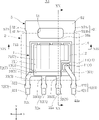
図1~図7は、本開示の第1実施形態に基づく半導体装置を示している。本実施形態の半導体装置A1は、半導体素子1、封止樹脂2、第1リード3、第2リード4、第3リード5および複数の導電性接合材6を備えている。半導体装置A1は、様々な電子機器などの回路基板に表面実装するものである。
1 to 7 show a semiconductor device according to a first embodiment of the present disclosure. A semiconductor device A1 of this embodiment includes a
図1は、半導体装置A1を示す平面図である。図2は、図1に示す平面図において封止樹脂2を透過した図である。図3は、図2の一部を拡大した要部拡大図である。なお、図3においては、各導電性接合材6を省略し、かつ、第1リード3および第2リード4を透過している。図4は、半導体装置A1を示す底面図である。図5は、図2に示すV-V線に沿う断面図である。図6は、図2に示すVI-VI線に沿う断面図である。図7は、図2に示すVII-VII線に沿う断面図である。説明の便宜上、互いに直交する3つの方向を、x方向、y方向、z方向とそれぞれ定義する。z方向は、半導体装置A1の厚さ方向である。x方向は、半導体装置A1の平面図における左右方向である。y方向は、半導体装置A1の平面図における上下方向である。x方向、y方向およびz方向が、特許請求の範囲に記載の「第2方向」、「第1方向」および「厚さ方向」にそれぞれ相当する。
FIG. 1 is a plan view showing the semiconductor device A1. FIG. 2 is a view through the sealing
半導体素子1は、半導体装置A1の電気的機能を発揮する要素である。本実施形態においては、半導体素子1は、3つの電極を有する3端子素子であり、たとえばパワーMOSFETである。なお、半導体素子1は、3端子素子に限定されず、ダイオードなどの2端子素子であってもよい。本実施形態においては、半導体素子1は、z方向に見て(以下、「平面視」ともいう。)矩形状である。半導体素子1の平面視寸法は、0.05~0.3mm角である。
The
半導体素子1は、素子主面10aおよび素子裏面10bを有する。素子主面10aおよび素子裏面10bは、z方向において離間しており、互いに反対側を向く。本実施形態においては、半導体装置A1を回路基板に実装した際、素子裏面10bが当該回路基板に対向する。素子主面10aおよび素子裏面10bはともに、平坦である。
The
半導体素子1は、ゲート電極11、ソース電極12、ドレイン電極13およびパッシベーション膜14を有している。本実施形態においては、ゲート電極11、ソース電極12およびドレイン電極13が、特許請求の範囲に記載の「第2電極」、「第1電極」および「第3電極」にそれぞれ相当する。また、パッシベーション膜14が、特許請求の範囲に記載の「絶縁膜」に相当する。
A
ゲート電極11およびソース電極12は、素子主面10aに形成されている。ゲート電極11の面積は、ソース電極12の面積よりも小さい。ドレイン電極13は、素子裏面10bに形成されている。
半導体素子1において、ゲート電極11は、パッド電極部111およびフィンガー電極部112を有する。パッド電極部111および複数のフィンガー電極部112は、半導体素子1の内部において導通している。
In
パッド電極部111は、第2リード4を接合するための部分である。パッド電極部111は、平面視矩形状である。各フィンガー電極部112は、ゲート電極11における内部抵抗(ゲート抵抗)を低減するためのものである。各フィンガー電極部112は、パッシベーション膜14に覆われている。これにより、各フィンガー電極部112は、半導体素子1の内部に配置されている。本実施形態においては、各フィンガー電極部112は、図3に示すように、y方向に沿って延びており、平面視矩形状である。また、図3に示すように、素子主面10aのy方向の一方(図3における上方)寄りに、3つのフィンガー電極部112がx方向に並んでおり、素子主面10aのy方向の他方(図3における下方)寄りに、2つのフィンガー電極部112がx方向に並んで配置されている。各フィンガー電極部112によって、ソース電極12がいくつかの領域に分割されている。
The
パッシベーション膜14は素子主面10aを覆うように形成された半導体素子1の保護膜である。パッシベーション膜14は、たとえばプラズマCVD法により形成されたSi3N4層やSiO2層、または、塗布により形成されたポリイミド樹脂層である。または、これらの組み合わせによって形成されたものでもよい。パッシベーション膜14から、ゲート電極11のパッド電極部111およびソース電極12がともに露出している。
The
封止樹脂2は、第1リード3、第2リード4および第3リード5のそれぞれ一部ずつと、半導体素子1とを覆っている。封止樹脂2は、たとえば黒色のエポキシ樹脂からなる。封止樹脂2は、たとえばモールド成形によって形成される。本実施形態においては、封止樹脂2は、平面視矩形状である。なお、封止樹脂2の素材、形成方法および形状はそれぞれ、上記したものに限定されない。封止樹脂2は、図1および図4~図7に示すように、樹脂主面21、樹脂裏面22および複数の樹脂側面23を有する。
The encapsulating
樹脂主面21と樹脂裏面22とは、厚さ方向zにおいて反対側を向く。樹脂主面21は、素子主面10aと同じ方向を向く。樹脂裏面22は、素子裏面10bと同じ方向を向く。複数の樹脂側面23は、樹脂主面21および樹脂裏面22に繋がっている。本実施形態においては、各樹脂側面23は、図5~図7に示すように、樹脂主面21および樹脂裏面22の両方に対して直交する。また、各樹脂側面23は、平坦である。なお、各樹脂側面23は、厚さ方向zに対して若干傾斜していてもよい。
The resin
第1リード3、第2リード4および第3リード5はそれぞれ、半導体素子1に導通する。第1リード3、第2リード4および第3リード5は、金属からなる。本実施形態においては、当該金属は、主な成分がCu(銅)であるものとするが、Ni(ニッケル)、または、CuやNiの合金、42アロイなどであってもよい。なお、第1リード3、第2リード4および第3リード5の各素材は、上記したものに限定されない。第1リード3、第2リード4および第3リード5は、たとえば金属プレス加工(スタンピング加工)によって所定の形状に形成される。
第1リード3は、半導体素子1のソース電極12に導通する導電部材である。本実施形態においては、第1リード3が、特許請求の範囲に記載の「第1導電部材」に相当する。第1リード3は、第1パッド部31、複数の第1露出部32および複数の第1連結部33を含んでいる。
The
第1パッド部31は、半導体素子1のソース電極12に接合するための部分である。第1パッド部31は、平面視において、ソース電極12に重なる。本実施形態においては、第1パッド部31は、封止樹脂2に覆われている。第1パッド部31は、第1パッド主面311および第1パッド接合面312を有し、さらに、複数の凹部313を含む。
The
第1パッド主面311は、図5および図6に示すように、半導体素子1の素子主面10aと同じ方向を向く。本実施形態においては、第1パッド主面311は平坦である。また、第1パッド主面311は、封止樹脂2に覆われている。
The first pad
第1パッド接合面312は、半導体素子1の素子裏面10bと同じ方向を向く。よって、第1パッド接合面312は、第1パッド主面311と反対側を向く。第1パッド接合面312は、半導体素子1に対向しており、一部の導電性接合材6(後述する第1接合材61)を介して、ソース電極12に接合されている。第1パッド接合面312が特許請求の範囲に記載の「接合面」に相当する。
The first
複数の凹部313はそれぞれ、第1パッド接合面312からz方向に窪んだ部分である。本実施形態においては、第1パッド部31には、3つの凹部313が形成されている。また、各凹部313は、図2に示すように、平面視においてy方向に延びている。本実施形態においては、各凹部313は、第1パッド部31のy方向の一方の端縁からy方向他方の端縁まで繋がる。各凹部313は、図3に示すように、平面視においてゲート電極11のフィンガー電極部112に重なる。本実施形態においては、凹部313が特許請求の範囲に記載の「非接合部」に相当する。各凹部313は、複数の凹部内面313aおよび凹部底面313bを有する。
Each of the plurality of
複数の凹部内面313aはそれぞれ、第1パッド接合面312から第1パッド主面311に向かって広がる。本実施形態においては、各凹部313は、2つの凹部内面313aを有する。各凹部内面313aは、平坦である。各凹部内面313aは、第1パッド接合面312および凹部底面313bの両方に直交する。なお、各凹部内面313aは、曲面であってもよいし、z方向に対して傾斜していてもよい。本実施形態においては、凹部内面313aが特許請求の範囲に記載の「内面」に相当する。
Each of the plurality of recess
凹部底面313bは、各凹部313における複数の凹部内面313aに繋がる。凹部底面313bは、第1パッド接合面312と同じ方向を向き、第1パッド接合面312よりもz方向において第1パッド主面311側に配置されている。本実施形態においては、凹部底面313bは、平坦である。なお、凹部底面313bは、平坦に限定されず、たとえば曲面であってもよい。
The
複数の第1露出部32はそれぞれ、封止樹脂2から露出する。本実施形態においては、各第1露出部32は、平面視において、封止樹脂2のy方向を向く2つの樹脂側面23の一方(平面図(図1参照)における下方)から突き出ている。本実施形態においては、第1露出部32は、3つある。なお、第1露出部32の数は限定されない。複数の第1露出部32は、x方向に並んでいる。複数の第1露出部32は、x方向に見て、互いに重なる。各第1露出部32は、図1、図2および図4に示すように、第1先端面32aを有している。第1先端面32aは、y方向の一方(図1において下方)を向く面である。本実施形態においては、各第1露出部32は、各第1先端面32aを除いて、めっき(図示略)で覆われている。よって、各第1先端面32aにおいて、第1リード3の素地(本実施形態においてはCu)が露出している。なお、各第1先端面32aもめっきで覆われていてもよい。各第1露出部32は、第1端子部321および第1屈曲部322を含んでいる。
Each of the plurality of first exposed
各第1端子部321は、半導体装置A1を回路基板等に実装する際の端子として機能する。本実施形態においては、第1リード3が半導体素子1のソース電極12に導通しているので、各第1端子部321は半導体装置A1におけるソース端子である。
Each first
各第1屈曲部322は、平面視において、y方向の一方の端縁が第1連結部33に繋がり、y方向の他方の端縁が第1端子部321に繋がる。各第1屈曲部322は、z方向に屈曲している。各第1屈曲部322は、ガルウィング状に曲げ加工が施されている。
Each first
複数の第1連結部33はそれぞれ、封止樹脂2に覆われている。各第1連結部33は、第1パッド部31と各第1露出部32とを繋いでいる。各第1連結部33は、各第1露出部32に対して形成されている。本実施形態においては、第1露出部32が3つあるので、第1連結部33も3つある。各第1連結部33は、z方向において、各第1端子部321よりも素子主面10aが向く方向に位置する。
Each of the plurality of first connecting
第2リード4は、半導体素子1のゲート電極11に導通する導電部材である。本実施形態においては、第2リード4が、特許請求の範囲に記載の「第2導電部材」に相当する。第2リード4は、第2パッド部41、第2露出部42および第2連結部43を含んでいる。
The
第2パッド部41は、半導体素子1のゲート電極11(パッド電極部111)に接合するための部分である。第2パッド部41は、平面視において半導体素子1のゲート電極11に重なる。第2パッド部41は、封止樹脂2に覆われている。本実施形態においては、第2パッド部41は、平面視矩形状である。第2パッド部41は、第2パッド主面411および第2パッド接合面412を有する。
The
第2パッド主面411は、図5および図7に示すように、半導体素子1の素子主面10aと同じ方向を向く。本実施形態においては、第2パッド主面411は平坦である。また、第2パッド主面411は、封止樹脂2に覆われている。
The second pad
第2パッド接合面412は、半導体素子1の素子裏面10bと同じ方向を向く。よって、第2パッド接合面412は、第2パッド主面411と反対側を向く。第2パッド接合面412は、半導体素子1に対向しており、一部の導電性接合材6(後述する第2接合材62)を介して、ゲート電極11に接合されている。
The second
第2露出部42は、封止樹脂2から露出する。本実施形態においては、第2露出部42は、平面視において、封止樹脂2のy方向を向く2つの樹脂側面23の一方(平面図(図1参照)における下方)から突き出ている。第2露出部42は、x方向に見て、各第1露出部32と重なる。第2露出部42は、図1、図2、図4および図7に示すように、第2先端面42aを有している。第2先端面42aは、y方向の一方(図1において下方)を向く面である。本実施形態においては、第2露出部42は、第2先端面42aを除いて、めっき(図示略)で覆われている。よって、第2先端面42aにおいて、第2リード4の素地(本実施形態においてはCu)が露出している。なお、第2先端面42aもめっきで覆われていてもよい。第2露出部42は、第2端子部421および第2屈曲部422を含んでいる。
The second exposed
第2端子部421は、半導体装置A1を回路基板等に実装する際の端子として機能する。本実施形態においては、第2リード4が半導体素子1のゲート電極11に導通しているので、第2端子部421は半導体装置A1におけるゲート端子である。
The second
第2屈曲部422は、平面視において、y方向の一方の端縁が第2連結部43に繋がり、y方向の他方の端縁が第2端子部421に繋がる。第2屈曲部422は、z方向に屈曲している。第2屈曲部422は、ガルウィング状に曲げ加工が施されている。
In plan view, the second
第2連結部43は、封止樹脂2に覆われている。第2連結部43は、第2パッド部41と第2露出部42とを繋いでいる。第2連結部43は、z方向において、第2端子部421よりも素子主面10aが向く方向に位置する。
The second connecting
第3リード5は、半導体素子1のドレイン電極13に導通する導電部材である。本実施形態においては、第3リード5が、特許請求の範囲に記載の「第3導電部材」に相当する。第3リード5は、板状であり、かつ、平面視矩形状である。第3リード5は、搭載面50a、実装面50bおよび実装面側凹部50cを有する。搭載面50aと実装面50bとは、z方向において、離間しており、かつ、互いに反対側を向く。
The
搭載面50aは、半導体素子1の素子主面10aと同じ方向を向く。搭載面50aには、半導体素子1が搭載されている。搭載面50aは封止樹脂2に覆われている。搭載面50aは、平坦である。
The mounting
実装面50bは、半導体素子1の素子裏面10bと同じ方向を向く。実装面50bは、半導体装置A1が回路基板に実装された際、当該回路基板に対向する。実装面50bは、封止樹脂2から露出している。実装面50bは、平坦である。本実施形態においては、第3リード5が半導体素子1のドレイン電極13と導通しているので、実装面50bは半導体装置A1のドレイン端子となる。
The mounting
実装面側凹部50cは、実装面50bからz方向に窪んだ部分である。本実施形態においては、実装面側凹部50cは、図4~図7に示すように、第3リード5のうち、平面視において、封止樹脂2に重なる部分であって、かつ、外側に形成されている。実装面側凹部50cによって、第3リード5は、厚肉な部分と薄肉な部分とを含んでいる。実装面側凹部50cは、封止樹脂2で覆われている。なお、第3リード5は、実装面側凹部50cを有していなくてよい。ただし、第3リード5に実装面側凹部50cがあることで、第3リード5が封止樹脂2から抜けることを抑制できる。
The mounting surface side
また、第3リード5は、平面視において封止樹脂2から露出した第3露出部52を含んでいる。第3露出部52は、図1、図2および図4に示すように、一対の露出側面521を有する。一対の露出側面521はそれぞれ、x方向において、互いに反対側を向く。一対の露出側面521はともに、露出側面第1部521aおよび露出側面第2部521bを含んでいる。各露出側面521において、露出側面第1部521aは平坦である。露出側面第2部521bは、露出側面第1部521aに繋がり、かつ、平面視において露出側面第1部521aから内方に陥入している。第3リード5のうち封止樹脂2から露出した部分は、各露出側面第1部521aを除いて、めっき(図示略)で覆われている。よって、各露出側面第1部521aにおいて、第3リード5の素地(本実施形態においてはCu)が露出している。なお、各露出側面第1部521aもめっきで覆われていてもよい。
Further, the
本実施形態においては、第3リード5には、貫通孔51が形成されている。なお、貫通孔51は、形成されていなくてもよい。貫通孔51には、封止樹脂2が充填されている。また、本実施形態においては、図2に示すように、貫通孔51は、平面視矩形状であるが、平面視形状は限定されない。貫通孔51は、z方向において、搭載面50aから実装面50bまで繋がる。
In this embodiment, a through
本実施形態においては、複数の第1端子部321および第2端子部421は、x方向に見て重なる。また、複数の第1端子部321および第2端子部421はそれぞれ、y方向に見て、第3リード5に重なる。本実施形態においては、複数の第1端子部321のz方向下面(素子裏面10bと同じ方向を向く面)、第2端子部421のz方向下面(素子裏面10bと同じ方向を向く面)および第3リード5の実装面50bとはz方向において略同じ位置に配置されている。これにより、半導体装置A1を回路基板に表面実装可能であるとともに、半導体装置A1を安定した姿勢で表面実装することができる。
In the present embodiment, the plurality of first
本実施形態においては、半導体素子1は、第1リード3および第2リード4と、第3リード5とによって、挟持されている。
In this embodiment, the
複数の導電性接合材6は、たとえばはんだあるいはAgペーストからなる。なお、各導電性接合材6の素材は、上記したものに限定されない。複数の導電性接合材6は、複数の第1接合材61、第2接合材62および第3接合材63を含む。
The plurality of
複数の第1接合材61はそれぞれ、第1パッド部31とソース電極12とを接合し、これらを導通させる。本実施形態においては、各第1接合材61は、第1パッド部31の第1パッド接合面312とソース電極12との間に介在する。
The plurality of
第2接合材62は、第2パッド部41とゲート電極11とを接合し、これらを導通させる。本実施形態においては、第2接合材62は、第2パッド部41の第2パッド接合面412とゲート電極11のパッド電極部111との間に介在する。
The second
第3接合材63は、第3リード5(搭載面50a)とドレイン電極13とを接合し、これらを導通させる。本実施形態においては、第3接合材63は、第3リード5の搭載面50aとドレイン電極13との間に介在する。
The third
次に、半導体装置A1の作用効果について説明する。 Next, functions and effects of the semiconductor device A1 will be described.
半導体装置A1によれば、第1リード3の第1パッド部31は、複数の凹部313を含んでいる。このような構成をとることで、第1パッド部31には、半導体素子1のソース電極12に接合されない非接合部が形成される。よって、半導体素子1が第1リード3(第1パッド部31)に拘束される領域を少なくできる。これにより、たとえば、第1リード3と半導体素子1との熱膨張係数の差により半導体素子1に加わる応力を緩和することができる。したがって、半導体素子1の破損を抑制できるため、半導体装置A1の信頼性が向上する。
According to the semiconductor device A1, the
半導体装置A1によれば、第1リード3の第1パッド部31に形成された複数の凹部313は、平面視において、半導体素子1のゲート電極11のフィンガー電極部112に重なる。従来の半導体装置においては、ソース電極12の略全面に接合材が配置(接合)されている。このような構成を半導体装置A1に適用した場合、フィンガー電極部112を覆うパッシベーション膜14上にも導電性接合材6(第1接合材61)が配置される。この結果、当該パッシベーション膜14と第1接合材61との素材の違いによる熱膨張係数の差により、半導体素子1が破損しうる。一方、本実施形態においては、上記するように、複数の凹部313が平面視においてフィンガー電極部112に重なるため、第1パッド部31に形成された各凹部313により、パッシベーション膜14上に第1接合材61が配置されない。したがって、半導体素子1の破損を抑制することができる。
According to the semiconductor device A1, the
半導体装置A1によれば、第1パッド部31には3つの凹部313が形成されている。また、半導体装置A1は、半導体素子1の平面視寸法が0.05~0.3mm角程度である。平面視寸法がこの大きさである半導体素子1においては、x方向に並ぶフィンガー電極部112は3つ以下となることが多い。すなわち、x方向に並ぶフィンガー電極部112が1つや2つの場合もある。たとえば、図8および図9は、x方向に並ぶフィンガー電極部112が1つの場合を示しており、図10および図11は、x方向に並ぶフィンガー電極部112が2つの場合を示している。図8および図10は、図3に対応する要部拡大図である。図9および図11は、図2のVI-VI線に沿う断面に対応する断面図(図6参照)である。これらの図に示すように、いずれの場合であっても、平面視において、フィンガー電極部112が複数の凹部313のいずれかに重なっている。したがって、半導体素子1に形成されたゲート電極11のフィンガー電極部112の配置によらず、上記した形状の第1リード3を利用できる。換言すれば、半導体素子1に応じて、第1リード3に形成された複数の凹部313の配置を変更する必要がないため、用いる半導体素子1に合わせて第1リード3を設計し直す必要がない。たとえば、半導体素子1が1つのフィンガー電極部112を有する場合、この1つのフィンガー電極部112上に、1つの凹部313が配置されるように第1パッド部31(第1リード3)を設計することが可能である。しかしながら、このように設計された第1リード3では、半導体素子1が2つのフィンガー電極部112を有する場合には、そのまま用いることができず、2つのフィンガー電極部112の配置に応じて、2つの凹部313が配置されるように第1パッド部31を設計する必要がある。したがって、半導体素子1に設けられたフィンガー電極部112に応じて、一品一様に第1リード3(第1パッド部31の凹部313の配置)を設計する必要がある。一方、半導体装置A1においては、第1パッド部31に複数の凹部313が形成されている。そのため、フィンガー電極部112の個数や配置が異なる半導体素子1であっても、第1リード3を流用できることがある。したがって、複数の凹部313が形成された第1パッド部31を含む第1リード3を用いることで、半導体装置A1の生産性の向上を図ることができる。
According to the semiconductor device A1, three
半導体装置A1によれば、第1パッド部31には複数の凹部313が形成されている。したがって、凹部313が形成されていない板状の場合と比較して、第1パッド部31の、y方向に直交する平面(x-z平面)における断面積を縮小するとともに、表面積を増大することができる。これにより、周波数の高い電流が第1パッド部31に流れた場合であっても、表皮効果による抵抗の増加を抑制することができる。
According to the semiconductor device A<b>1 , a plurality of
半導体装置A1によれば、第1リード3が半導体素子1のソース電極12に直接接合されている。したがって、ボンディングワイヤやボンディングリボンを介して導通する場合よりも、半導体装置A1の内部抵抗を低減することができる。同様に、半導体装置A1においては、第2リード4が半導体素子1のゲート電極11に直接接合されている。したがって、ボンディングワイヤやボンディングリボンを介して導通する場合よりも、半導体装置A1の内部抵抗を低減することができる。
According to the semiconductor device A<b>1 , the
半導体装置A1によれば、第1リード3は封止樹脂2から露出した第1露出部32を含んでおり、第1露出部32は、第1屈曲部322によって屈曲している。このような構成をとることで、半導体装置A1を回路基板に実装した際に加わる応力を、第1屈曲部322によって緩和させることができる。
According to the semiconductor device A<b>1 , the
第1実施形態では、各フィンガー電極部112がy方向に延びた矩形状である場合を示したが、各フィンガー電極部112の形状はこれに限定されない。たとえば、フィンガー電極部112は、平面視において、ソース電極12のうち、第1パッド部31の非接合部(凹部313)に重なる領域に形成されていればよい。すなわち、平面視において、非接合部(凹部313)に重なる領域内であれば、フィンガー電極部112を自由に配置することができる。
In the first embodiment, each
以下に、本開示の半導体装置にかかる他の実施形態について説明する。なお、以下に示す他の実施形態において、上記第1実施形態と同一または類似の要素には、同じ符号を付してその説明を省略する。 Other embodiments of the semiconductor device of the present disclosure will be described below. In other embodiments described below, elements that are the same as or similar to those of the first embodiment are denoted by the same reference numerals, and description thereof will be omitted.
図12および図13は、第2実施形態にかかる半導体装置を示している。本実施形態の半導体装置A2は、上記半導体装置A1(第1実施形態)と比較して、第1パッド部31に、複数の凹部313の代わりに複数の貫通孔314が形成されている点で異なる。
12 and 13 show the semiconductor device according to the second embodiment. The semiconductor device A2 of this embodiment differs from the semiconductor device A1 (first embodiment) in that a plurality of through
図12は、半導体装置A2を示す平面図である。なお、図12においては、封止樹脂2を透過している。図13は、図12のXIII-XIII線に沿う断面図である。図13は、第1実施形態における図6に示す断面に対応する。
FIG. 12 is a plan view showing the semiconductor device A2. In addition, in FIG. 12, the sealing
複数の貫通孔314はそれぞれ、z方向において第1パッド接合面312から第1パッド主面311まで繋がっている。本実施形態においては、各貫通孔314は、平面視において、y方向に延びる矩形状である。なお、各貫通孔314の平面視形状は、矩形状に限定されず、多角形状あるいは円形状などであってもよい。本実施形態においては、各貫通孔314は、貫通孔内面314aを有する。
Each of the plurality of through
貫通孔内面314aは、z方向において、第1パッド接合面312から第1パッド主面311まで繋がる。本実施形態においては、貫通孔内面314aは平坦である。また、貫通孔内面314aは、第1パッド接合面312および第1パッド主面311のそれぞれに直交する。よって、貫通孔内面314aは、z方向に対して平行である。なお、貫通孔内面314aは、z方向に対して傾斜していてもよい。本実施形態においては、貫通孔314が特許請求の範囲に記載の「非接合部」に相当し、貫通孔内面314aが特許請求の範囲に記載の「内面」に相当する。
The through hole
半導体装置A2によれば、第1リード3の第1パッド部31は、複数の貫通孔314を含んでいる。このような構成をとることで、第1パッド部31には、半導体素子1のソース電極12に接合されない非接合部が形成される。したがって、半導体装置A2は、半導体装置A1と同様に、半導体素子1の破損を抑制できるため、半導体装置A2の信頼性が向上する。また、半導体装置A2において、半導体装置A1と同様に構成された部分は、半導体装置A1と同様の効果を奏することができる。
According to the semiconductor device A2, the
半導体装置A2によれば、第1パッド部31には複数の貫通孔314が形成されている。したがって、上記複数の凹部313と同様に、第1パッド部31の、x-z平面における断面積を縮小するとともに、表面積を増大することができる。したがって、周波数の高い電流が流れる場合、表皮効果による低抵抗化を図ることができる。
According to the semiconductor device A2, a plurality of through
なお、半導体装置A2の通電時に、半導体素子1が発熱し、この半導体素子1から発生する熱は、第1パッド部31に伝達する。本実施形態にかかる第1パッド部31は、貫通孔314が形成されており、第1実施形態のように凹部313が形成された第1パッド部31と比較して、その容積が減少する。よって、半導体素子1から発生した熱が伝達する経路が少なくなる。したがって、第1パッド部31に複数の凹部313が形成されている方が、複数の貫通孔314が形成されている場合よりも、半導体素子1から発生する熱の放熱性を向上させることができる。
When the semiconductor device A2 is energized, the
図14および図15は、第3実施形態にかかる半導体装置を示している。本実施形態の半導体装置A3は、上記半導体装置A1(第1実施形態)と比較して、第1パッド部31の第1パッド主面311の一部が露出している点で異なる。
14 and 15 show the semiconductor device according to the third embodiment. The semiconductor device A3 of this embodiment differs from the semiconductor device A1 (first embodiment) in that a portion of the first pad
図14は、半導体装置A3を示す平面図である。図15は、図14のXV-XV線に沿う断面図である。図15は、第1実施形態における図6に示す断面に対応する。 FIG. 14 is a plan view showing the semiconductor device A3. 15 is a cross-sectional view along line XV-XV of FIG. 14. FIG. FIG. 15 corresponds to the cross section shown in FIG. 6 in the first embodiment.
本実施形態においては、封止樹脂2は、図15に示すように、樹脂主面21からz方向に窪んだ樹脂凹部25を有する。樹脂凹部25によって、封止樹脂2の樹脂主面21は開口している。本実施形態においては、樹脂凹部25は、平面視矩形状である。樹脂凹部25は、図14および図15に示すように、第1パッド部31の第1パッド主面311の一部を露出させている。樹脂凹部25は、樹脂凹部底面25aおよび樹脂凹部側面25bを有する。
In this embodiment, as shown in FIG. 15, the sealing
樹脂凹部底面25aは、半導体素子1の素子主面10aと同じ方向を向く。樹脂凹部底面25aは、図15に示すように、z方向において、樹脂主面21と樹脂裏面22との間に位置する。樹脂凹部底面25aと第1パッド主面311とは図15に示すように面一である。
Resin
樹脂凹部側面25bは、z方向において、一方の端縁が樹脂主面21に繋がり、他方の端縁が樹脂凹部底面25aに繋がる。ただし、本実施形態においては、図14のy方向下側の樹脂凹部側面25bにおいて、上記他方の端縁の一部は第1パッド主面311に接している。樹脂凹部側面25bは、平坦である。本実施形態においては、樹脂凹部側面25bは、樹脂主面21および樹脂凹部底面25aの両方に対して直交する。樹脂凹部側面25bは、z方向に対して平行である。なお、樹脂凹部側面25bは、z方向に対して傾斜していてもよい。
The resin
半導体装置A3によれば、半導体装置A1と同様に、第1リード3の第1パッド部31は、複数の凹部313を含んでいる。このような構成をとることで、第1パッド部31には、半導体素子1のソース電極12に接合されない非接合部が形成される。したがって、半導体装置A3は、半導体装置A1と同様に、半導体素子1の破損を抑制できるため、半導体装置A3の信頼性が向上する。また、半導体装置A3において、半導体装置A1,A2と同様に構成された部分は、半導体装置A1,A2と同様の効果を奏することができる。
According to the semiconductor device A3, similarly to the semiconductor device A1, the
半導体装置A3によれば、封止樹脂2には、樹脂凹部25が形成されており、当該樹脂凹部25において、第1パッド部31の第1パッド主面311の一部が封止樹脂2から露出している。半導体装置A3の通電時に、この半導体素子1から発生した熱は、第1パッド部31に伝達する。よって、上記するように第1パッド主面311の一部を封止樹脂2から露出させたことで、半導体素子1から発生した熱を効率よく外部に放出することが可能となる。すなわち、半導体装置A3は、半導体装置A1と比較して、放熱性が向上する。
According to the semiconductor device A3, the
第3実施形態では、樹脂凹部25が樹脂凹部底面25aを有する場合を示したが、これを有していなくてもよい。図16および図17は、このような変形例にかかる半導体装置A3’を示している。図16は、半導体装置A3’を示す平面図であり、図14に対応する。図17は、図16のXVII-XVII線に沿う断面図であり、図15に対応する。
Although the
半導体装置A3’においては、樹脂凹部25の樹脂凹部側面25bは、図17に示すように、z方向において、一方の端縁が樹脂主面21に繋がり、他方の端縁が第1パッド主面311に接している。このような場合であっても、上記半導体装置A3と同様の効果を奏することができる。
In the semiconductor device A3′, as shown in FIG. 17, one edge of the resin
なお、第3実施形態およびその変形例においては、樹脂凹部25によって、第1パッド主面311の一部を封止樹脂2から露出させる場合を示したが、これに限定されない。たとえば、封止樹脂2の厚みを全体的に薄くすることで、第1パッド主面311の少なくとも一部を露出させるようにしてもよい。この場合、樹脂主面21と第1パッド主面311とが面一となる。ただし、この場合においては、第2リード4の第2パッド主面411も同様に封止樹脂2から露出する。よって、第1リード3と第2リード4との意図せぬ短絡を抑制するために、次のような対策を講じるとよい。それは、第2パッド主面411を絶縁体で覆うか、第2パッド主面411が封止樹脂2から露出しないように、第2パッド主面411を第1パッド主面311よりもz方向下方に配置させるなどである。
In addition, in the third embodiment and its modified example, the case where a part of the first pad
図18~図20は、第4実施形態にかかる半導体装置を示している。本実施形態の半導体装置A4は、上記半導体装置A1(第1実施形態)と比較して、第1リード3と半導体素子1のソース電極12とが、板状の金属部材(以下、「ストラップ部材7」という。)を介して、導通している点で異なる。
18 to 20 show the semiconductor device according to the fourth embodiment. In the semiconductor device A4 of the present embodiment, compared with the semiconductor device A1 (first embodiment), the
図18は、半導体装置A4を示す平面図である。なお、図18においては、封止樹脂2を透過している。図19は、図18のXIX-XIX線に沿う断面図である。図19は、第1実施形態における図6に示す断面に対応する。図20は、図18のXX-XX線に沿う断面図である。
FIG. 18 is a plan view showing the semiconductor device A4. In addition, in FIG. 18, the sealing
本実施形態においては、第1リード3は、帯状部34と複数の第1露出部32と複数の第1連結部33とを含んでいる。帯状部34は、ストラップ部材7が接合される部分である。本実施形態においては、帯状部34は、平面視においてx方向に延びる矩形状である。本実施形態においては、各第1連結部33は、帯状部34と各第1露出部32とにそれぞれ繋がる。各第1連結部33は、帯状部34のy方向一方(図18における下方)の端縁から延びる。
In this embodiment, the
ストラップ部材7は、上記するように板状の金属部材である。本実施形態においては、ストラップ部材7は、第1リード3の帯状部34と半導体素子1のソース電極12とにそれぞれ接合されている。ストラップ部材7は、そのすべてが封止樹脂2に覆われている。本実施形態においては、ストラップ部材7が特許請求の範囲に記載の「第1導電部材」に相当する。ストラップ部材7は、第1クリップ接合部71、第2クリップ接合部72および屈曲部73を含んでいる。
The
第1クリップ接合部71は、半導体素子1のソース電極12に接合するための部分である。第1クリップ接合部71は、上記第1リード3の第1パッド部31と同様に構成される。本実施形態においては、第1クリップ接合部71が特許請求の範囲に記載の「第1パッド部」に相当する。第1クリップ接合部71は、ストラップ主面711、ストラップ接合面712および複数の凹部713を有する。ストラップ主面711、ストラップ接合面712および複数の凹部713は、上記第1パッド部31における第1パッド主面311、第1パッド接合面312および複数の凹部313とそれぞれ同様に構成される。本実施形態においては、ストラップ接合面712が特許請求の範囲に記載の「接合面」に相当する。半導体素子1は、ストラップ部材7の第1クリップ接合部71と第3リード5とにより挟持されている。
The first clip
第2クリップ接合部72は、第1リード3の帯状部34に接合するための部分である。第2クリップ接合部72は、導電性接合材6(第4接合材64)を介して、帯状部34に接合されている。第4接合材64は、たとえばはんだあるいはAgペーストからなる。なお、第4接合材64の素材は、上記したものに限定されない。
The second
屈曲部73は、第1クリップ接合部71と第2クリップ接合部72とに繋がる。本実施形態においては、第1クリップ接合部71と第2クリップ接合部72とは、z方向において異なる位置に配置されている。したがって、屈曲部73は、これらを繋ぐように、z方向に屈曲している。
The
半導体装置A4によれば、ストラップ部材7の第1クリップ接合部71は、複数の凹部713を含んでいる。このような構成をとることで、第1クリップ接合部71には、半導体素子1のソース電極12に接合されない非接合部が形成される。よって、半導体素子1がストラップ部材7(第1クリップ接合部71)に拘束される領域を少なくできる。これにより、ストラップ部材7と半導体素子1との熱膨張係数の差により半導体素子1に加わる応力を緩和することができる。したがって、半導体素子1の破損を抑制できるため、半導体装置A4の信頼性が向上する。すなわち、上記第1実施形態と同様の効果を奏することができる。また、半導体装置A4において、半導体装置A1~A3と同様に構成された部分は、半導体装置A1~A3と同様の効果を奏することができる。
According to semiconductor device A4, first clip
第4実施形態においては、第1リード3とソース電極12とをストラップ部材7を介して、接続した場合を示したが、これに限定されない。たとえば、第2リード4とゲート電極11とを、ストラップ部材7と同様のストラップ部材で接続してもよい。
In the fourth embodiment, the case where the
第3実施形態および第4実施形態においては、上記第1実施形態と同様に、第1パッド部31に複数の凹部313が形成されている場合を示したが、第2実施形態と同様に、複数の凹部313の代わりに複数の貫通孔314が形成されていてもよい。
In the third and fourth embodiments, as in the first embodiment, a plurality of
第1実施形態ないし第4実施形態においては、半導体装置A1~A4のパッケージは図示したものに限定されない。本開示にかかる半導体装置は、その他の表面実装型パッケージあるいはピン挿入型パッケージなどであってもよい。 In the first through fourth embodiments, the packages of the semiconductor devices A1 through A4 are not limited to those illustrated. The semiconductor device according to the present disclosure may be other surface mount type packages or pin insertion type packages.
第1実施形態ないし第4実施形態においては、平面視において、第1パッド部31の非接合部(凹部313あるいは貫通孔314)がゲート電極11のフィンガー電極部112に重なる場合を示したが、これに限定されない。半導体素子1において、第1パッド部31によって接合したくない領域がある場合には、上記非接合部が当該領域に重なるように構成してもよい。このような変形例の一例について、図21を参照して、以下に説明する。
In the first to fourth embodiments, the case where the non-bonding portion (
図21は、当該変形例にかかる要部拡大平面図であり、第1実施形態における図3に対応する。図21に示す半導体素子1は、ゲート電極11、ソース電極12およびドレイン電極13がともに、素子主面10aに形成されている。そして、素子主面10aにおいて、ソース電極12およびドレイン電極13がそれぞれ櫛歯状に形成されている。
FIG. 21 is an enlarged plan view of a main part according to the modification, and corresponds to FIG. 3 in the first embodiment. A
ソース電極12は、パッド電極部121および複数のフィンガー電極部122を有する。パッド電極部121は、平面視において、x方向に延びる矩形状である。複数のフィンガー電極部122は、平面視矩形状であり、パッド電極部121のy方向の一方(図21における上方)側の端縁からy方向に延びている。パッド電極部121および複数のフィンガー電極部122はともに、パッシベーション膜14から露出している。
The
ドレイン電極13は、パッド電極部131および複数のフィンガー電極部132を有する。パッド電極部131は、平面視において、x方向に延びる矩形状である。当該変形例においては、図21に示すように、パッド電極部131と第3リード5(搭載面50a)とがストラップ部材7’で接合されている。なお、ストラップ部材7’に限定されず、ボンディングワイヤあるいはボンディングリボンであってもよい。複数のフィンガー電極部132は、平面視矩形状であり、パッド電極部131のy方向一方(図21における下方)側の端縁からy方向に延びている。パッド電極部131および複数のフィンガー電極部132はともに、パッシベーション膜14から露出している。
The
複数のフィンガー電極部122と複数のフィンガー電極部132とは、x方向において交互に並んでいる。また、隣り合うフィンガー電極部122とフィンガー電極部132との離間距離はともに等しい。
The plurality of
このように構成されたソース電極12に対して、従来のように、非接合部(たとえば複数の凹部313)がない第1パッド部31で全面接合すると、ドレイン電極13にも接合される。その結果、ソース電極12とドレイン電極13とが短絡する。一方、図21に示す変形例においては、第1パッド部31に非接合部(たとえば複数の凹部313)が形成されており、当該非接合部は平面視においてドレイン電極13のフィンガー電極部132に重なる。これにより、ソース電極12のフィンガー電極部122には、第1パッド部31が接合され、ドレイン電極13のフィンガー電極部132には、第1パッド部31が接合されないように構成できる。したがって、ソース電極12とドレイン電極13との短絡を防止することができる。
When the entire surface of the
また、図21に示す変形例においては、第1パッド部31の非接合部(複数の凹部313)は、第1パッド部31のy方向の一方(図21における下方)側の端縁まで繋がっていない。これにより、第1パッド部31は、ソース電極12のパッド電極部121の略全面に接合できる。したがって、第1パッド部31は、ソース電極12のパッド電極部121および複数のフィンガー電極部122の略全面に接合されているため、内部抵抗の低減を図ることができる。
In the modification shown in FIG. 21, the non-bonded portions (plurality of concave portions 313) of the
さらに、図21に示す変形例においては、第1パッド部31の非接合部(複数の凹部313)は、平面視において、ゲート電極11のフィンガー電極部112に重なっている。したがって、ゲート電極11のフィンガー電極部112を覆うパッシベーション膜14と第1接合材61との熱膨張係数の差による半導体素子1の破損を抑制することができる。
Furthermore, in the modification shown in FIG. 21, the non-bonding portions (plurality of recesses 313) of the
なお、上記した変形例においては、半導体素子1の素子主面10aのうち、図21に示す上寄りにドレイン電極13が形成されており、図21に示す下寄りにソース電極12が形成されている場合を示したが、反対であってもよい。すなわち、図21に示す上寄りにソース電極12が形成されており、図21に示す下寄りにドレイン電極13が形成されていてもよい。この場合、第1リード3の第1端子部321はドレイン端子になる。
In the modified example described above, the
本開示にかかる半導体装置は、上記した実施形態に限定されるものではない。本開示の半導体装置の各部の具体的な構成は、種々に設計変更自在である。 The semiconductor device according to the present disclosure is not limited to the above-described embodiments. The specific configuration of each part of the semiconductor device of the present disclosure can be changed in various ways.
A1~A4,A3’:半導体装置
1 :半導体素子
10a :素子主面
10b :素子裏面
11 :ゲート電極
111 :パッド電極部
112 :フィンガー電極部
12 :ソース電極
121 :パッド電極部
122 :フィンガー電極部
13 :ドレイン電極
131 :パッド電極部
132 :フィンガー電極部
14 :パッシベーション膜
2 :封止樹脂
21 :樹脂主面
22 :樹脂裏面
23 :樹脂側面
25 :樹脂凹部
25a :樹脂凹部底面
25b :樹脂凹部側面
3 :第1リード
31 :第1パッド部
311 :第1パッド主面
312 :第1パッド接合面
313 :凹部
313a :凹部内面
313b :凹部底面
314 :貫通孔
314a :貫通孔内面
32 :第1露出部
32a :第1先端面
321 :第1端子部
322 :第1屈曲部
33 :第1連結部
34 :帯状部
4 :第2リード
41 :第2パッド部
411 :第2パッド主面
412 :第2パッド接合面
42 :第2露出部
42a :第2先端面
421 :第2端子部
422 :第2屈曲部
43 :第2連結部
5 :第3リード
50a :搭載面
50b :実装面
51 :貫通孔
52 :第3露出部
521 :露出側面
521a :露出側面第1部
521b :露出側面第2部
6 :導電性接合材
61 :第1接合材
62 :第2接合材
63 :第3接合材
64 :第4接合材
7,7’ :ストラップ部材
71 :第1クリップ接合部
711 :ストラップ主面
712 :ストラップ接合面
713 :凹部
72 :第2クリップ接合部
73 :屈曲部
A1 to A4, A3': semiconductor device 1: semiconductor element 10a: element main surface 10b: element back surface 11: gate electrode 111: pad electrode portion 112: finger electrode portion 12: source electrode 121: pad electrode portion 122: finger electrode portion 13: Drain electrode 131: Pad electrode portion 132: Finger electrode portion 14: Passivation film 2: Sealing resin 21: Resin main surface 22: Resin back surface 23: Resin side surface 25: Resin recess 25a: Resin recess bottom surface 25b: Resin recess side surface 3: first lead 31: first pad portion 311: first pad main surface 312: first pad bonding surface 313: recess 313a: recess inner surface 313b: recess bottom surface 314: through hole 314a: through hole inner surface 32: first exposure Portion 32a : First tip surface 321 : First terminal portion 322 : First bent portion 33 : First connecting portion 34 : Strip portion 4 : Second lead 41 : Second pad portion 411 : Second pad main surface 412 : Second terminal portion 322 2-pad bonding surface 42 : second exposed portion 42a : second tip surface 421 : second terminal portion 422 : second bent portion 43 : second connecting portion 5 : third lead 50a : mounting surface 50b : mounting surface 51 : penetration Hole 52: Third exposed portion 521: Exposed side surface 521a: First exposed side surface portion 521b: Second exposed side surface portion 6: Conductive bonding material 61: First bonding material 62: Second bonding material 63: Third bonding material 64 : fourth joint material 7, 7' : strap member 71 : first clip joint portion 711 : strap main surface 712 : strap joint surface 713 : concave portion 72 : second clip joint portion 73 : bending portion
Claims (17)
前記第1電極に電気的に接続された第1導電部材と、
前記第2電極に電気的に接続された第2導電部材と、
前記第1導電部材の一部、前記第2導電部材の一部、および、前記半導体素子を覆う封止樹脂と、を備えており、
前記第1導電部材は、前記厚さ方向に見て前記半導体素子のほぼ全域に重なる第1パッド部を含んでおり、
前記第1パッド部は、前記第1電極に接合された接合面および前記厚さ方向において前記接合面と反対側を向く第1パッド主面を有しており、さらに、前記接合面から前記第1パッド主面に向かって広がる内面を有し、かつ、前記第1電極に接合されない非接合部を含んでいる、
ことを特徴とする半導体装置。 a semiconductor element having an element main surface and an element back surface facing opposite sides in a thickness direction, and having a first electrode and a second electrode formed on the element main surface;
a first conductive member electrically connected to the first electrode;
a second conductive member electrically connected to the second electrode;
a part of the first conductive member, a part of the second conductive member, and a sealing resin covering the semiconductor element;
The first conductive member includes a first pad portion that overlaps substantially the entire area of the semiconductor element when viewed in the thickness direction,
The first pad portion has a bonding surface bonded to the first electrode and a first pad main surface facing the opposite side of the bonding surface in the thickness direction. 1 having an inner surface that spreads toward the main surface of the pad and includes a non-bonding portion that is not bonded to the first electrode;
A semiconductor device characterized by:
前記非接合部は、前記厚さ方向に見て、前記フィンガー電極部に重なる、
請求項1に記載の半導体装置。 The second electrode has a pad electrode portion to which the second conductive member is joined, and a finger electrode portion for reducing internal resistance of the second electrode,
The non-joint portion overlaps the finger electrode portion when viewed in the thickness direction,
A semiconductor device according to claim 1 .
請求項2に記載の半導体装置。 The semiconductor element has an insulating film covering the finger electrode portion,
3. The semiconductor device according to claim 2.
請求項2または請求項3のいずれか一項に記載の半導体装置。 The semiconductor element is 0.05 to 0.3 mm square when viewed in the thickness direction,
4. The semiconductor device according to claim 2 or 3.
請求項1ないし請求項4のいずれか一項に記載の半導体装置。 The first conductive member has a first exposed portion protruding from the sealing resin when viewed in the thickness direction, and is covered with the sealing resin and connected to the first pad portion and the first exposed portion. further comprising a first connection;
5. The semiconductor device according to claim 1.
請求項5に記載の半導体装置。 The first exposed portion includes a first bent portion connected to the first connecting portion and bent in the thickness direction, and a first terminal portion connected to the first bent portion.
6. The semiconductor device according to claim 5.
前記半導体素子は、前記素子裏面に第3電極が形成されており、
前記第3導電部材は、前記第3電極に電気的に接続している、
請求項6に記載の半導体装置。 Further comprising a third conductive member on which the semiconductor element is mounted,
The semiconductor element has a third electrode formed on the back surface of the element,
the third conductive member is electrically connected to the third electrode;
7. The semiconductor device according to claim 6.
前記第3導電部材は、前記素子裏面と同じ方向を向き、かつ、前記樹脂裏面から露出する実装面を有しており、
前記第1端子部は、前記厚さ方向に直交する第1方向に見て、前記第3導電部材に重なる、
請求項7に記載の半導体装置。 The sealing resin has a resin back surface facing the same direction as the element back surface,
The third conductive member has a mounting surface facing the same direction as the element back surface and exposed from the resin back surface,
The first terminal portion overlaps the third conductive member when viewed in a first direction orthogonal to the thickness direction,
8. The semiconductor device according to claim 7.
請求項8に記載の半導体装置。 The second conductive member includes a second pad portion joined to the second electrode, a second exposed portion protruding from the sealing resin when viewed in the thickness direction, and covered with the sealing resin, and a second connecting portion connected to the second pad portion and the second exposed portion,
9. The semiconductor device according to claim 8.
請求項9に記載の半導体装置。 The second exposed portion includes a second bent portion connected to the second connecting portion and bent in the thickness direction, and a second terminal portion connected to the second bent portion.
10. The semiconductor device according to claim 9.
請求項10に記載の半導体装置。 The second terminal portion overlaps the third conductive member when viewed in the first direction,
11. The semiconductor device according to claim 10.
請求項1ないし請求項11のいずれか一項に記載の半導体装置。 The non-joint portion further includes a bottom surface connected to the inner surface and facing in the same direction as the joint surface,
12. The semiconductor device according to claim 1.
請求項12に記載の半導体装置。 The non-bonded portion is a plurality of recesses each extending in a first direction orthogonal to the thickness direction and arranged in a second direction orthogonal to both the thickness direction and the first direction. ,
13. The semiconductor device according to claim 12.
請求項13に記載の半導体装置。 each of the plurality of recesses is connected from an edge of the first pad portion on one side in the first direction to an edge on the other side in the first direction;
14. The semiconductor device according to claim 13.
請求項1ないし請求項14のいずれか一項に記載の半導体装置。 At least a portion of the first pad main surface is exposed from the sealing resin,
15. The semiconductor device according to claim 1.
前記樹脂凹部は、樹脂凹部底面、および、当該樹脂凹部底面と前記樹脂主面とに繋がる樹脂凹部側面を有しており、
前記樹脂凹部底面と前記第1パッド主面とが面一である、
請求項15に記載の半導体装置。 The sealing resin has a resin main surface facing in the same direction as the element main surface and a resin recess recessed from the resin main surface,
The resin recess has a resin recess bottom surface and a resin recess side surface connecting the resin recess bottom surface and the resin main surface,
The bottom surface of the resin recess and the main surface of the first pad are flush with each other,
16. The semiconductor device according to claim 15.
前記第1電極は、ソース電極であり、
前記第2電極は、ゲート電極である、
請求項1ないし請求項16のいずれか一項に記載の半導体装置。 The semiconductor device is a power MOSFET,
the first electrode is a source electrode;
wherein the second electrode is a gate electrode;
17. The semiconductor device according to claim 1.
Priority Applications (5)
| Application Number | Priority Date | Filing Date | Title |
|---|---|---|---|
| JP2018082981A JP7150461B2 (en) | 2018-04-24 | 2018-04-24 | semiconductor equipment |
| US16/388,021 US11031322B2 (en) | 2018-04-24 | 2019-04-18 | Semiconductor device mounted on circuit board of electronic device |
| US17/308,401 US11742264B2 (en) | 2018-04-24 | 2021-05-05 | Semiconductor device |
| JP2022154130A JP7441287B2 (en) | 2018-04-24 | 2022-09-27 | semiconductor equipment |
| US18/349,496 US20230352375A1 (en) | 2018-04-24 | 2023-07-10 | Semiconductor device |
Applications Claiming Priority (1)
| Application Number | Priority Date | Filing Date | Title |
|---|---|---|---|
| JP2018082981A JP7150461B2 (en) | 2018-04-24 | 2018-04-24 | semiconductor equipment |
Related Child Applications (1)
| Application Number | Title | Priority Date | Filing Date |
|---|---|---|---|
| JP2022154130A Division JP7441287B2 (en) | 2018-04-24 | 2022-09-27 | semiconductor equipment |
Publications (2)
| Publication Number | Publication Date |
|---|---|
| JP2019192751A JP2019192751A (en) | 2019-10-31 |
| JP7150461B2 true JP7150461B2 (en) | 2022-10-11 |
Family
ID=68237048
Family Applications (2)
| Application Number | Title | Priority Date | Filing Date |
|---|---|---|---|
| JP2018082981A Active JP7150461B2 (en) | 2018-04-24 | 2018-04-24 | semiconductor equipment |
| JP2022154130A Active JP7441287B2 (en) | 2018-04-24 | 2022-09-27 | semiconductor equipment |
Family Applications After (1)
| Application Number | Title | Priority Date | Filing Date |
|---|---|---|---|
| JP2022154130A Active JP7441287B2 (en) | 2018-04-24 | 2022-09-27 | semiconductor equipment |
Country Status (2)
| Country | Link |
|---|---|
| US (3) | US11031322B2 (en) |
| JP (2) | JP7150461B2 (en) |
Families Citing this family (8)
| Publication number | Priority date | Publication date | Assignee | Title |
|---|---|---|---|---|
| JP7150461B2 (en) * | 2018-04-24 | 2022-10-11 | ローム株式会社 | semiconductor equipment |
| US11069600B2 (en) * | 2019-05-24 | 2021-07-20 | Infineon Technologies Ag | Semiconductor package with space efficient lead and die pad design |
| JP7359581B2 (en) * | 2019-07-10 | 2023-10-11 | 株式会社デンソー | semiconductor equipment |
| JP2021150334A (en) * | 2020-03-16 | 2021-09-27 | 株式会社東芝 | Semiconductor device and manufacturing method of the same |
| JP6952824B2 (en) * | 2020-04-06 | 2021-10-27 | 三菱電機株式会社 | Power modules and power semiconductor devices using them |
| DE112021002615T5 (en) * | 2020-08-05 | 2023-03-23 | Rohm Co., Ltd. | SEMICONDUCTOR COMPONENT |
| JP2022186276A (en) * | 2021-06-04 | 2022-12-15 | 株式会社デンソー | Semiconductor device |
| WO2023100659A1 (en) * | 2021-12-01 | 2023-06-08 | ローム株式会社 | Semiconductor device |
Citations (11)
| Publication number | Priority date | Publication date | Assignee | Title |
|---|---|---|---|---|
| JP2004006967A (en) | 2003-07-28 | 2004-01-08 | Denso Corp | Semiconductor device |
| JP2005277168A (en) | 2004-03-25 | 2005-10-06 | Nec Electronics Corp | Semiconductor device, its assembling method, and conductive adhesive for semiconductor device |
| JP2007037892A (en) | 2005-08-05 | 2007-02-15 | Matsushita Electric Ind Co Ltd | Remote medical system |
| JP2007184525A (en) | 2005-12-07 | 2007-07-19 | Mitsubishi Electric Corp | Electronic apparatus |
| JP2007266218A (en) | 2006-03-28 | 2007-10-11 | Renesas Technology Corp | Semiconductor device, and its manufacturing method |
| JP2009516389A (en) | 2005-11-18 | 2009-04-16 | フェアチャイルド セミコンダクター コーポレイション | Semiconductor die package using lead frame and clip, and manufacturing method |
| US20110102059A1 (en) | 2008-05-19 | 2011-05-05 | X-Fab Semiconductor Foundries Ag | Location-Related Adjustment of the Operatng Temperature Distribution or Power Distribution of a Semiconductor Power Component, and Component for Carrying Out Said Method |
| WO2015045648A1 (en) | 2013-09-30 | 2015-04-02 | 富士電機株式会社 | Semiconductor device, method for assembling semiconductor device, component for semiconductor devices and unit module |
| JP2016036047A (en) | 2015-11-04 | 2016-03-17 | トヨタ自動車株式会社 | Power module |
| WO2016071982A1 (en) | 2014-11-06 | 2016-05-12 | 三菱電機株式会社 | Semiconductor module and conductive member for semiconductor module |
| JP2018061009A (en) | 2016-09-30 | 2018-04-12 | ローム株式会社 | Semiconductor device and semiconductor package |
Family Cites Families (11)
| Publication number | Priority date | Publication date | Assignee | Title |
|---|---|---|---|---|
| WO2000049656A1 (en) | 1999-02-17 | 2000-08-24 | Hitachi, Ltd. | Semiconductor device and method of manufacture thereof |
| JP4078993B2 (en) | 2003-01-27 | 2008-04-23 | 三菱電機株式会社 | Semiconductor device |
| JP2006202931A (en) | 2005-01-20 | 2006-08-03 | Renesas Technology Corp | Semiconductor device and its manufacturing method |
| JP2006310609A (en) | 2005-04-28 | 2006-11-09 | Toshiba Corp | Semiconductor device |
| JP2009004435A (en) | 2007-06-19 | 2009-01-08 | Toshiba Corp | Semiconductor device |
| JP4804497B2 (en) | 2008-03-24 | 2011-11-02 | ルネサスエレクトロニクス株式会社 | Semiconductor device |
| JP2011192760A (en) | 2010-03-12 | 2011-09-29 | Nec Corp | Semiconductor device and method of manufacturing the same |
| JP2012182240A (en) | 2011-02-28 | 2012-09-20 | Panasonic Corp | Semiconductor device |
| JP6386746B2 (en) | 2014-02-26 | 2018-09-05 | 株式会社ジェイデバイス | Semiconductor device |
| JP6150866B2 (en) | 2015-11-02 | 2017-06-21 | 三菱電機株式会社 | Power semiconductor device |
| JP7150461B2 (en) * | 2018-04-24 | 2022-10-11 | ローム株式会社 | semiconductor equipment |
-
2018
- 2018-04-24 JP JP2018082981A patent/JP7150461B2/en active Active
-
2019
- 2019-04-18 US US16/388,021 patent/US11031322B2/en active Active
-
2021
- 2021-05-05 US US17/308,401 patent/US11742264B2/en active Active
-
2022
- 2022-09-27 JP JP2022154130A patent/JP7441287B2/en active Active
-
2023
- 2023-07-10 US US18/349,496 patent/US20230352375A1/en active Pending
Patent Citations (11)
| Publication number | Priority date | Publication date | Assignee | Title |
|---|---|---|---|---|
| JP2004006967A (en) | 2003-07-28 | 2004-01-08 | Denso Corp | Semiconductor device |
| JP2005277168A (en) | 2004-03-25 | 2005-10-06 | Nec Electronics Corp | Semiconductor device, its assembling method, and conductive adhesive for semiconductor device |
| JP2007037892A (en) | 2005-08-05 | 2007-02-15 | Matsushita Electric Ind Co Ltd | Remote medical system |
| JP2009516389A (en) | 2005-11-18 | 2009-04-16 | フェアチャイルド セミコンダクター コーポレイション | Semiconductor die package using lead frame and clip, and manufacturing method |
| JP2007184525A (en) | 2005-12-07 | 2007-07-19 | Mitsubishi Electric Corp | Electronic apparatus |
| JP2007266218A (en) | 2006-03-28 | 2007-10-11 | Renesas Technology Corp | Semiconductor device, and its manufacturing method |
| US20110102059A1 (en) | 2008-05-19 | 2011-05-05 | X-Fab Semiconductor Foundries Ag | Location-Related Adjustment of the Operatng Temperature Distribution or Power Distribution of a Semiconductor Power Component, and Component for Carrying Out Said Method |
| WO2015045648A1 (en) | 2013-09-30 | 2015-04-02 | 富士電機株式会社 | Semiconductor device, method for assembling semiconductor device, component for semiconductor devices and unit module |
| WO2016071982A1 (en) | 2014-11-06 | 2016-05-12 | 三菱電機株式会社 | Semiconductor module and conductive member for semiconductor module |
| JP2016036047A (en) | 2015-11-04 | 2016-03-17 | トヨタ自動車株式会社 | Power module |
| JP2018061009A (en) | 2016-09-30 | 2018-04-12 | ローム株式会社 | Semiconductor device and semiconductor package |
Also Published As
| Publication number | Publication date |
|---|---|
| US20210257281A1 (en) | 2021-08-19 |
| US11742264B2 (en) | 2023-08-29 |
| JP7441287B2 (en) | 2024-02-29 |
| US11031322B2 (en) | 2021-06-08 |
| JP2019192751A (en) | 2019-10-31 |
| US20190326204A1 (en) | 2019-10-24 |
| US20230352375A1 (en) | 2023-11-02 |
| JP2022177252A (en) | 2022-11-30 |
Similar Documents
| Publication | Publication Date | Title |
|---|---|---|
| JP7150461B2 (en) | semiconductor equipment | |
| KR101614669B1 (en) | Electric power semiconductor device | |
| JP7210868B2 (en) | semiconductor equipment | |
| JP7137955B2 (en) | semiconductor equipment | |
| JP2015056638A (en) | Semiconductor device and method of manufacturing the same | |
| CN105448860B (en) | Semiconductor device | |
| JP2017123360A (en) | Semiconductor module | |
| JP7178184B2 (en) | semiconductor equipment | |
| WO2021241304A1 (en) | Mounting structure for semiconductor module | |
| JP5147295B2 (en) | Semiconductor device | |
| JP7144112B2 (en) | semiconductor equipment | |
| WO2023100759A1 (en) | Semiconductor device | |
| CN113056813A (en) | Semiconductor device with a plurality of semiconductor chips | |
| WO2023100659A1 (en) | Semiconductor device | |
| WO2023100681A1 (en) | Semiconductor device | |
| US11842951B2 (en) | Semiconductor device for improving heat dissipation and mounting structure thereof | |
| WO2023100663A1 (en) | Semiconductor device | |
| JP2019050297A (en) | Semiconductor device | |
| WO2023100731A1 (en) | Semiconductor device | |
| JP7385414B2 (en) | semiconductor equipment | |
| JP6254807B2 (en) | Semiconductor device and electronic equipment | |
| WO2021002225A1 (en) | Semiconductor device | |
| JP2022179872A (en) | Semiconductor device | |
| KR20240048469A (en) | Semiconductor device | |
| JP2024055042A (en) | Semiconductor Device |
Legal Events
| Date | Code | Title | Description |
|---|---|---|---|
| A621 | Written request for application examination |
Free format text: JAPANESE INTERMEDIATE CODE: A621 Effective date: 20210324 |
|
| A977 | Report on retrieval |
Free format text: JAPANESE INTERMEDIATE CODE: A971007 Effective date: 20220217 |
|
| A131 | Notification of reasons for refusal |
Free format text: JAPANESE INTERMEDIATE CODE: A131 Effective date: 20220222 |
|
| A521 | Request for written amendment filed |
Free format text: JAPANESE INTERMEDIATE CODE: A523 Effective date: 20220411 |
|
| TRDD | Decision of grant or rejection written | ||
| A01 | Written decision to grant a patent or to grant a registration (utility model) |
Free format text: JAPANESE INTERMEDIATE CODE: A01 Effective date: 20220830 |
|
| A61 | First payment of annual fees (during grant procedure) |
Free format text: JAPANESE INTERMEDIATE CODE: A61 Effective date: 20220928 |
|
| R150 | Certificate of patent or registration of utility model |
Ref document number: 7150461 Country of ref document: JP Free format text: JAPANESE INTERMEDIATE CODE: R150 |