JP7144591B2 - power converter - Google Patents
power converter Download PDFInfo
- Publication number
- JP7144591B2 JP7144591B2 JP2021192078A JP2021192078A JP7144591B2 JP 7144591 B2 JP7144591 B2 JP 7144591B2 JP 2021192078 A JP2021192078 A JP 2021192078A JP 2021192078 A JP2021192078 A JP 2021192078A JP 7144591 B2 JP7144591 B2 JP 7144591B2
- Authority
- JP
- Japan
- Prior art keywords
- auxiliary
- terminal
- switching element
- reactor
- node
- Prior art date
- Legal status (The legal status is an assumption and is not a legal conclusion. Google has not performed a legal analysis and makes no representation as to the accuracy of the status listed.)
- Active
Links
Images


Classifications
-
- Y—GENERAL TAGGING OF NEW TECHNOLOGICAL DEVELOPMENTS; GENERAL TAGGING OF CROSS-SECTIONAL TECHNOLOGIES SPANNING OVER SEVERAL SECTIONS OF THE IPC; TECHNICAL SUBJECTS COVERED BY FORMER USPC CROSS-REFERENCE ART COLLECTIONS [XRACs] AND DIGESTS
- Y02—TECHNOLOGIES OR APPLICATIONS FOR MITIGATION OR ADAPTATION AGAINST CLIMATE CHANGE
- Y02B—CLIMATE CHANGE MITIGATION TECHNOLOGIES RELATED TO BUILDINGS, e.g. HOUSING, HOUSE APPLIANCES OR RELATED END-USER APPLICATIONS
- Y02B70/00—Technologies for an efficient end-user side electric power management and consumption
- Y02B70/10—Technologies improving the efficiency by using switched-mode power supplies [SMPS], i.e. efficient power electronics conversion e.g. power factor correction or reduction of losses in power supplies or efficient standby modes
Description
電力変換装置に関し、特に、半導体スイッチング素子のソフトスイッチングを行なう電力変換装置に関する。
BACKGROUND OF THE
近年、電力変換装置の大容量化および高周波スイッチング化に伴ない、主回路の半導体スイッチング素子のスイッチング損失および電磁干渉(EMI)ノイズの増大が大きな問題となってきている。スイッチング損失およびEMIノイズを低減させる方法として、共振型電力変換装置が用いられており、種々の回路構成が提案されている。 In recent years, with the increase in capacity and high-frequency switching of electric power converters, an increase in switching loss and electromagnetic interference (EMI) noise in semiconductor switching elements in main circuits has become a serious problem. As a method for reducing switching loss and EMI noise, resonant power converters have been used, and various circuit configurations have been proposed.
共振型電力変換装置の代表例としては、電力変換装置に補助共振回路を設け、補助共振回路の共振動作により半導体スイッチング素子をソフトスイッチングさせる、補助共振転流ポール方式の電力変換装置が存在する(たとえば特開2011-55580号公報(特許文献1)参照)。 As a representative example of the resonance type power conversion device, there is an auxiliary resonance commutation pole type power conversion device in which an auxiliary resonance circuit is provided in the power conversion device, and the semiconductor switching element is soft-switched by the resonance operation of the auxiliary resonance circuit ( For example, see Japanese Patent Application Laid-Open No. 2011-55580 (Patent Document 1)).
上記の特許文献1に記載される共振型電力変換装置は、直列接続された2つの半導体スイッチング素子からなるハーフブリッジ回路を複数並列に接続したフルブリッジ構成のインバータである。特許文献1では、複数のハーフブリッジ回路の各々に対して補助共振回路を設けることで、各ハーフブリッジ回路を構成する半導体スイッチング素子のソフトスイッチングを実現している。
The resonance type power conversion device described in
しかしながら、複数のハーフブリッジ回路にそれぞれ対応するように、複数の補助共振回路を設ける必要があり、電力変換装置の構成が複雑かつ大型化することが懸念される。この発明はこのような課題を解決するためになされたものであって、その目的は、直流電力および交流電力の間で電力変換を行なう電力変換装置において、簡易な構成で半導体スイッチング素子のスイッチング損失およびEMIノイズを低減することができる新たな構成を提供することである。 However, it is necessary to provide a plurality of auxiliary resonance circuits so as to correspond to the plurality of half bridge circuits, respectively, and there is concern that the configuration of the power conversion device will become complicated and large. SUMMARY OF THE INVENTION The present invention has been made to solve such problems, and an object of the present invention is to reduce the switching loss of a semiconductor switching element with a simple configuration in a power converter that performs power conversion between DC power and AC power. and to provide a new configuration capable of reducing EMI noise.
本発明に係る電力変換装置は、直流電力および交流電力の間で電力変換を行なう電力変換装置であって、高電位側直流端子および低電位側直流端子と、高電位側直流端子および第1のノードの間に接続された第1のスイッチング素子と、第1のノードおよび低電位側直流端子の間に接続された第2のスイッチング素子と、高電位側直流端子および第2のノードの間に接続された第3のスイッチング素子と、第2のノードおよび低電位側直流端子の間に接続された第4のスイッチング素子と、第1のノードに電気的に接続された第1の交流端子と、第2のノードに電気的に接続された第2の交流端子と、第1から第4のスイッチング素子のオンオフを制御する制御回路とを備える。制御回路は、第3および第4のスイッチング素子を、交流周波数に同期してオンオフさせるとともに、第1および第2のスイッチング素子を、交流周波数よりも高い周波数でオンオフさせる。 A power conversion device according to the present invention is a power conversion device that performs power conversion between DC power and AC power, and includes a high potential side DC terminal and a low potential side DC terminal, a high potential side DC terminal and a first A first switching element connected between the nodes, a second switching element connected between the first node and the low potential side DC terminal, and between the high potential side DC terminal and the second node. a connected third switching element, a fourth switching element connected between the second node and the low potential side DC terminal, and a first AC terminal electrically connected to the first node; , a second AC terminal electrically connected to the second node, and a control circuit for controlling ON/OFF of the first to fourth switching elements. The control circuit turns on and off the third and fourth switching elements in synchronization with the AC frequency, and turns on and off the first and second switching elements at a frequency higher than the AC frequency.
好ましくは、電力変換装置は、第1のスイッチング素子に並列に接続された第1のキャパシタと、第2のスイッチング素子に並列に接続された第2のキャパシタと、補助共振回路とをさらに備える。補助共振回路は、リアクトルを含み、第1および第2のキャパシタとリアクトルとの共振動作により第1および第2のスイッチング素子をソフトスイッチングさせるように構成される。 Preferably, the power conversion device further includes a first capacitor connected in parallel with the first switching element, a second capacitor connected in parallel with the second switching element, and an auxiliary resonance circuit. The auxiliary resonant circuit includes a reactor and is configured to soft-switch the first and second switching elements by resonant operation of the first and second capacitors and the reactor.
好ましくは、補助共振回路は、高電位側直流端子および低電位側直流端子の間に電気的に直列に接続された第1および第2の補助スイッチング素子をさらに含む。リアクトルは、第1および第2の補助スイッチング素子の接続ノードと第1のノードとの間に電気的に接続される。 Preferably, the auxiliary resonant circuit further includes first and second auxiliary switching elements electrically connected in series between the high potential side DC terminal and the low potential side DC terminal. The reactor is electrically connected between a connection node of the first and second auxiliary switching elements and the first node.
好ましくは、補助共振回路は、高電位側直流端子および低電位側直流端子の間に電気的に直列に接続された第3および第4のキャパシタをさらに含む。リアクトルは、第3および第4のキャパシタの接続ノードと第1のノードとの間に電気的に接続される。補助共振回路は、第3および第4のキャパシタの接続ノードと第1のノードとの間にリアクトルと電気的に直列に接続された双方向スイッチをさらに含む。 Preferably, the auxiliary resonant circuit further includes third and fourth capacitors electrically connected in series between the high potential side DC terminal and the low potential side DC terminal. The reactor is electrically connected between a connection node of the third and fourth capacitors and the first node. The auxiliary resonant circuit further includes a bidirectional switch electrically connected in series with the reactor between a connection node of the third and fourth capacitors and the first node.
好ましくは、補助共振回路は、高電位側直流端子および低電位側直流端子の間に電気的に接続された一次巻線と、第1のノードおよび低電位側直流端子の間にリアクトルと電気的に直列に接続された二次巻線とを有する第1のトランスと、一次巻線および低電位側直流端子の間に電気的に接続された第1の補助スイッチング素子と、二次巻線および低電位側直流端子の間に電気的に接続された第2の補助スイッチング素子とを含む。 Preferably, the auxiliary resonant circuit includes a primary winding electrically connected between the high-potential DC terminal and the low-potential DC terminal, and a reactor electrically connected between the first node and the low-potential DC terminal. a first transformer having a secondary winding connected in series with a first auxiliary switching element electrically connected between the primary winding and the low potential side DC terminal; the secondary winding and and a second auxiliary switching element electrically connected between the low potential side DC terminals.
好ましくは、第1のトランスの一次巻線および二次巻線の巻線比は2:1である。 Preferably, the turns ratio of the primary and secondary windings of the first transformer is 2:1.
好ましくは、第1のトランスは、高電位側直流端子および低電位側直流端子の間に電気的に接続されたリセット巻線を有する。補助共振回路は、低電位側直流端子から高電位側直流端子に向かう方向を順方向として、高電位側直流端子および低電位側直流端子の間にリセット巻線と電気的に直列に接続されたダイオードをさらに含む。 Preferably, the first transformer has a reset winding electrically connected between the high side DC terminal and the low side DC terminal. The auxiliary resonant circuit is electrically connected in series with the reset winding between the high potential side DC terminal and the low potential side DC terminal, with the direction from the low potential side DC terminal to the high potential side DC terminal being the forward direction. Further includes a diode.
好ましくは、補助共振回路は、高電位側直流端子および低電位側直流端子の間に電気的に直列に接続された第1および第2の補助スイッチング素子をさらに含む。リアクトルは、第1および第2の補助スイッチング素子の接続ノードと第1のノードとの間に電気的に接続される。補助共振回路は、低電位側直流端子から高電位側直流端子に向かう方向を順方向として、低電位側直流端子および高電位側直流端子の間に電気的に直列に接続された第1および第2のダイオードと、低電位側直流端子から高電位側直流端子に向かう方向を順方向として、低電位側直流端子および高電位側直流端子の間に電気的に直列に接続された第3および第4のダイオードと、第2のトランスとをさらに含む。第2のトランスは、第1および第2の補助スイッチング素子の接続ノードと第1のノードとの間にリアクトルと電気的に直列に接続された一次巻線と、第1および第2のダイオードの接続ノードと前記第3および第4のダイオードの接続ノードとの間に電気的に接続された二次巻線とを有する。 Preferably, the auxiliary resonant circuit further includes first and second auxiliary switching elements electrically connected in series between the high potential side DC terminal and the low potential side DC terminal. The reactor is electrically connected between a connection node of the first and second auxiliary switching elements and the first node. The auxiliary resonant circuit has first and first electrically connected in series between the low potential side DC terminal and the high potential side DC terminal, with the direction from the low potential side DC terminal to the high potential side DC terminal being the forward direction. 2, and the third and third diodes electrically connected in series between the low potential side DC terminal and the high potential side DC terminal, with the direction from the low potential side DC terminal to the high potential side DC terminal being the forward direction. 4 diodes and a second transformer. The second transformer includes a primary winding electrically connected in series with a reactor between a connection node of the first and second auxiliary switching elements and the first node, and first and second diodes. It has a secondary winding electrically connected between the connection node and the connection node of the third and fourth diodes.
好ましくは、第2のトランスの一次巻線および二次巻線の巻線比は1:2である。 Preferably, the turns ratio of the primary and secondary windings of the second transformer is 1:2.
好ましくは、補助共振回路は、第5のダイオードと、第6のダイオードとをさらに含む。第5のダイオードは、高電位側直流端子および第1および第2の補助スイッチング素子の接続ノードとの間に、第1の補助スイッチング素子と電気的に直列に接続される。第6のダイオードは、低電位側直流端子および第1および第2の補助スイッチング素子の接続ノードとの間に、第2の補助スイッチング素子と電気的に直列に接続される。 Preferably, the auxiliary resonant circuit further includes a fifth diode and a sixth diode. The fifth diode is electrically connected in series with the first auxiliary switching element between the high potential side DC terminal and the connection node of the first and second auxiliary switching elements. The sixth diode is electrically connected in series with the second auxiliary switching element between the low potential side DC terminal and the connection node of the first and second auxiliary switching elements.
好ましくは、第1および第2のスイッチング素子の各々は、第1の電力用半導体スイッチング素子と、第1の電力用半導体スイッチング素子に逆並列に接続された第1の還流ダイオードとを有する。第3および第4のスイッチング素子の各々は、第2の電力用半導体スイッチング素子と、第2の電力用半導体スイッチング素子に逆並列に接続された第2の還流ダイオードとを有する。第1の還流ダイオードは、第2の還流ダイオードに比べて逆回復時間が短い。 Preferably, each of the first and second switching elements has a first power semiconductor switching element and a first free wheel diode connected in anti-parallel to the first power semiconductor switching element. Each of the third and fourth switching elements has a second power semiconductor switching element and a second free wheel diode connected in anti-parallel to the second power semiconductor switching element. The first freewheeling diode has a shorter reverse recovery time than the second freewheeling diode.
好ましくは、第1の還流ダイオードは、ワイドバンドギャップ半導体によって形成される。 Preferably, the first freewheeling diode is formed by a wide bandgap semiconductor.
好ましくは、制御回路は、パルス幅変調制御によって、第1および第2のスイッチング素子のオンオフを制御するための制御信号を生成する。 Preferably, the control circuit generates a control signal for controlling on/off of the first and second switching elements by pulse width modulation control.
本発明に係る電力変換装置は、高電位側直流端子および低電位側直流端子と、高電位側直流端子および第1のノードの間に電気的に接続された第1のスイッチング素子と、第1のノードおよび低電位側直流端子の間に電気的に接続された第2のスイッチング素子と、第1のノードに電気的に接続された交流端子と、第1のスイッチング素子に並列に接続された第1のキャパシタと、第2のスイッチング素子に並列に接続された第2のキャパシタと、リアクトルを含み、第1および第2のキャパシタとリアクトルとの共振動作により第1および第2のスイッチング素子をソフトスイッチングさせるように構成された補助共振回路とを備える。補助共振回路は、高電位側直流端子および低電位側直流端子の間に電気的に直列に接続された第1および第2の補助スイッチング素子をさらに含む。リアクトルは、第1および第2の補助スイッチング素子の接続ノードと第1のノードとの間に電気的に接続される。 A power converter according to the present invention includes a high-potential DC terminal, a low-potential DC terminal, a first switching element electrically connected between the high-potential DC terminal and a first node, a first a second switching element electrically connected between the node of and the low potential side DC terminal; an AC terminal electrically connected to the first node; and a first switching element connected in parallel to a first capacitor, a second capacitor connected in parallel to a second switching element, and a reactor, wherein resonance operations of the first and second capacitors and the reactor operate the first and second switching elements an auxiliary resonant circuit configured for soft switching. The auxiliary resonant circuit further includes first and second auxiliary switching elements electrically connected in series between the high potential side DC terminal and the low potential side DC terminal. The reactor is electrically connected between a connection node of the first and second auxiliary switching elements and the first node.
本発明に係る電力変換装置は、高電位側直流端子および低電位側直流端子と、高電位側直流端子および第1のノードの間に電気的に接続された第1のスイッチング素子と、第1のノードおよび低電位側直流端子の間に電気的に接続された第2のスイッチング素子と、第1のノードに電気的に接続された交流端子と、第1のスイッチング素子に並列に接続された第1のキャパシタと、第2のスイッチング素子に並列に接続された第2のキャパシタと、リアクトルを含み、第1および第2のキャパシタとリアクトルとの共振動作により第1および第2のスイッチング素子をソフトスイッチングさせるように構成された補助共振回路とを備える。補助共振回路は、高電位側直流端子および低電位側直流端子の間に電気的に接続された一次巻線と、第1のノードおよび低電位側直流端子の間にリアクトルと電気的に直列に接続された二次巻線とを有する第1のトランスと、一次巻線および低電位側直流端子の間に電気的に接続された第1の補助スイッチング素子と、二次巻線および低電位側直流端子の間に電気的に接続された第2の補助スイッチング素子とを含む。 A power converter according to the present invention includes a high-potential DC terminal, a low-potential DC terminal, a first switching element electrically connected between the high-potential DC terminal and a first node, a first a second switching element electrically connected between the node of and the low potential side DC terminal; an AC terminal electrically connected to the first node; and a first switching element connected in parallel to a first capacitor, a second capacitor connected in parallel to a second switching element, and a reactor, wherein resonance operations of the first and second capacitors and the reactor operate the first and second switching elements an auxiliary resonant circuit configured for soft switching. The auxiliary resonant circuit includes a primary winding electrically connected between the high-potential DC terminal and the low-potential DC terminal, and a reactor electrically connected in series between the first node and the low-potential DC terminal. a first transformer having a connected secondary winding; a first auxiliary switching element electrically connected between the primary winding and the low side DC terminal; the secondary winding and the low side; and a second auxiliary switching element electrically connected between the DC terminals.
好ましくは、第1のトランスの前記一次巻線および二次巻線の巻線比は2:1である。 Preferably, the turns ratio of said primary and secondary windings of the first transformer is 2:1.
好ましくは、第1のトランスは、高電位側直流端子および低電位側直流端子の間に電気的に接続されたリセット巻線を有する。補助共振回路は、低電位側直流端子から高電位側直流端子に向かう方向を順方向として、高電位側直流端子および低電位側直流端子の間にリセット巻線と電気的に直列に接続されたダイオードをさらに含む。 Preferably, the first transformer has a reset winding electrically connected between the high side DC terminal and the low side DC terminal. The auxiliary resonant circuit is electrically connected in series with the reset winding between the high potential side DC terminal and the low potential side DC terminal, with the direction from the low potential side DC terminal to the high potential side DC terminal being the forward direction. Further includes a diode.
本発明に係る電力変換装置は、高電位側直流端子および低電位側直流端子と、高電位側直流端子および第1のノードの間に電気的に接続された第1のスイッチング素子と、第1のノードおよび低電位側直流端子の間に電気的に接続された第2のスイッチング素子と、第1のノードに電気的に接続された交流端子と、第1のスイッチング素子に並列に接続された第1のキャパシタと、第2のスイッチング素子に並列に接続された第2のキャパシタと、リアクトルを含み、第1および第2のキャパシタとリアクトルとの共振動作により第1および第2のスイッチング素子をソフトスイッチングさせるように構成された補助共振回路とを備える。補助共振回路は、高電位側直流端子および低電位側直流端子の間に電気的に直列に接続された第1および第2の補助スイッチング素子をさらに含む。リアクトルは、第1および第2の補助スイッチング素子の接続ノードと第1のノードとの間に電気的に接続される。補助共振回路は、低電位側直流端子から高電位側直流端子に向かう方向を順方向として、低電位側直流端子および高電位側直流端子の間に電気的に直列に接続された第1および第2のダイオードと、低電位側直流端子から高電位側直流端子に向かう方向を順方向として、低電位側直流端子および高電位側直流端子の間に電気的に直列に接続された第3および第4のダイオードと、第1および第2の補助スイッチング素子の接続ノードと第1のノードとの間にリアクトルと電気的に直列に接続された一次巻線と、第1および第2のダイオードの接続ノードと前記第3および第4のダイオードの接続ノードとの間に電気的に接続された二次巻線とを有する第2のトランスとをさらに含む。 A power converter according to the present invention includes a high-potential DC terminal, a low-potential DC terminal, a first switching element electrically connected between the high-potential DC terminal and a first node, a first a second switching element electrically connected between the node of and the low potential side DC terminal; an AC terminal electrically connected to the first node; and a first switching element connected in parallel to a first capacitor, a second capacitor connected in parallel to a second switching element, and a reactor, wherein resonance operations of the first and second capacitors and the reactor operate the first and second switching elements an auxiliary resonant circuit configured for soft switching. The auxiliary resonant circuit further includes first and second auxiliary switching elements electrically connected in series between the high potential side DC terminal and the low potential side DC terminal. The reactor is electrically connected between a connection node of the first and second auxiliary switching elements and the first node. The auxiliary resonant circuit has first and first electrically connected in series between the low potential side DC terminal and the high potential side DC terminal, with the direction from the low potential side DC terminal to the high potential side DC terminal being the forward direction. 2, and the third and third diodes electrically connected in series between the low potential side DC terminal and the high potential side DC terminal, with the direction from the low potential side DC terminal to the high potential side DC terminal being the forward direction. 4 diodes, a primary winding electrically connected in series with a reactor between a connection node of the first and second auxiliary switching elements and the first node, and a connection of the first and second diodes. A second transformer having a secondary winding electrically connected between a node and a connection node of the third and fourth diodes.
好ましくは、第2のトランスの一次巻線および二次巻線の巻線比は1:2である。 Preferably, the turns ratio of the primary and secondary windings of the second transformer is 1:2.
好ましくは、補助共振回路は、高電位側直流端子および第1および第2の補助スイッチング素子の接続ノードとの間に、第1の補助スイッチング素子と電気的に直列に接続された第5のダイオードと、低電位側直流端子および前記第1および第2の補助スイッチング素子の接続ノードとの間に、第2の補助スイッチング素子と電気的に直列に接続された第6のダイオードとをさらに含む。 Preferably, the auxiliary resonant circuit includes a fifth diode electrically connected in series with the first auxiliary switching element between the high potential side DC terminal and the connection node of the first and second auxiliary switching elements. and a connection node between the low potential side DC terminal and the first and second auxiliary switching elements, a sixth diode electrically connected in series with the second auxiliary switching element.
この発明によれば、直流電力および交流電力の間で電力変換を行なう電力変換装置において、簡易な構成で半導体スイッチング素子のスイッチング損失およびEMIノイズを低減することができる。 According to the present invention, it is possible to reduce switching loss and EMI noise of a semiconductor switching element with a simple configuration in a power converter that performs power conversion between DC power and AC power.
以下、本発明の実施の形態について図面を参照して詳細に説明する。なお以下では図中の同一または相当部分には同一符号を付して、その説明は原則的に繰返さないものとする。 BEST MODE FOR CARRYING OUT THE INVENTION Hereinafter, embodiments of the present invention will be described in detail with reference to the drawings. In the following description, the same reference numerals are given to the same or corresponding parts in the drawings, and the description thereof will not be repeated in principle.
[実施の形態1]
図1は、この発明の実施の形態1に従う電力変換装置1の主回路構成図である。本実施の形態1に従う電力変換装置1は、直流電力および交流電力の間で双方向の電力変換を行なうAC/DCコンバータである。
[Embodiment 1]
FIG. 1 is a main circuit configuration diagram of a
図1を参照して、本実施の形態1に従う電力変換装置1は、直流端子T1,T2と、交流端子T3,T4と、電力用半導体スイッチング素子(以下、単に「スイッチング素子」とも称する)Q1~Q4と、キャパシタC0,C5と、リアクトルL1と、制御回路5とを備える。
Referring to FIG. 1,
直流端子T1(高電位側直流端子)は直流電源P1の正極端子と電気的に接続され、直流端子T2(低電位側直流端子)は直流電源P1の負極端子と電気的に接続される。直流端子T1には直流正母線PL1が接続され、直流端子T2には直流負母線NL1が接続される。交流端子T3およびT4の間には、交流系統P2が電気的に接続される。本明細書において「電気的に接続」とは、直接的な接続、あるいは、他要素を介した接続によって電気エネルギの伝達が可能な接続状態を示すものとする。 The DC terminal T1 (high potential side DC terminal) is electrically connected to the positive terminal of the DC power supply P1, and the DC terminal T2 (low potential side DC terminal) is electrically connected to the negative terminal of the DC power supply P1. DC positive bus PL1 is connected to DC terminal T1, and DC negative bus NL1 is connected to DC terminal T2. An AC system P2 is electrically connected between AC terminals T3 and T4. In this specification, the term "electrically connected" indicates a connected state in which electrical energy can be transmitted by direct connection or connection via another element.
スイッチング素子Q1は、直流正母線PL1(すなわち直流端子T1)およびノードaの間に電気的に接続される。スイッチング素子Q2は、ノードaおよび直流負母線NL1(すなわち直流端子T2)の間に電気的に接続される。ノードaは交流端子T3と電気的に接続される。ノードaは「第1のノード」に対応し、交流端子T3は「第1の交流端子」に対応する。 Switching element Q1 is electrically connected between DC positive bus PL1 (that is, DC terminal T1) and node a. Switching element Q2 is electrically connected between node a and DC negative bus NL1 (that is, DC terminal T2). Node a is electrically connected to AC terminal T3. The node a corresponds to the "first node", and the AC terminal T3 corresponds to the "first AC terminal".
スイッチング素子Q3は、直流正母線PL1およびノードbの間に電気的に接続される。スイッチング素子Q4は、ノードbおよび直流負母線NL1の間に電気的に接続される。ノードbは交流端子T4と電気的に接続される。ノードbは「第2のノード」に対応し、交流端子T4は「第2の交流端子」に対応する。 Switching element Q3 is electrically connected between DC positive bus PL1 and node b. Switching element Q4 is electrically connected between node b and DC negative bus NL1. Node b is electrically connected to AC terminal T4. The node b corresponds to the "second node", and the AC terminal T4 corresponds to the "second AC terminal".
なお、図1では、スイッチング素子として、MOSFET(Metal Oxide Semiconductor Field Effect Transistor)を用いているが、IGBT(Insulated Gate Bipolar Transistor)などの任意の自己消弧型のスイッチング素子を用いることができる。スイッチング素子Q1~Q4にはそれぞれ、ダイオードD1~D4が逆並列に接続されている。ダイオードD1~D4の各々は、対応するスイッチング素子のオフ時にフリーホイール電流を流すために設けられている。スイッチング素子がMOSFETである場合、フリーホイールダイオードは寄生のダイオード(ボディダイオード)で構成してもよい。スイッチング素子がダイオードを内蔵しないIGBTである場合、フリーホイールダイオードはIGBTに逆並列に接続されたダイオードで構成される。 In FIG. 1, MOSFETs (Metal Oxide Semiconductor Field Effect Transistors) are used as switching elements, but arbitrary self-extinguishing switching elements such as IGBTs (Insulated Gate Bipolar Transistors) can be used. Diodes D1 to D4 are connected in anti-parallel to the switching elements Q1 to Q4, respectively. Each of the diodes D1-D4 is provided to flow a freewheel current when the corresponding switching element is off. If the switching element is a MOSFET, the freewheel diode may be composed of a parasitic diode (body diode). If the switching element is an IGBT with no built-in diode, the freewheel diode is composed of a diode connected in anti-parallel to the IGBT.
スイッチング素子Q1およびQ2は、「第1ハーフブリッジ回路A」を構成する。スイッチング素子Q3およびQ4は、「第2ハーフブリッジ回路B」を構成する。第1ハーフブリッジ回路Aおよび第2ハーフブリッジ回路Bは、直流正母線PL1および直流負母線NL1の間に互いに並列に接続される。すなわち、電力変換装置1はフルブリッジ回路を有する。
Switching elements Q1 and Q2 form a "first half bridge circuit A". Switching elements Q3 and Q4 form a "second half bridge circuit B". First half bridge circuit A and second half bridge circuit B are connected in parallel between DC positive bus PL1 and DC negative bus NL1. That is, the
キャパシタC0は、直流正母線PL1および直流負母線NL1の間に接続され、直流端子T1およびT2間の電圧(すなわち直流電源P1の出力電圧)を平滑化する。 Capacitor C0 is connected between DC positive bus PL1 and DC negative bus NL1, and smoothes the voltage between DC terminals T1 and T2 (that is, the output voltage of DC power supply P1).
リアクトルL1は、ノードa(第1のノード)および交流端子T3の間に接続される。キャパシタC5は、交流端子T3およびT4の間に接続される。交流端子T3およびT4間の電圧を平滑化する。リアクトルL1およびキャパシタC5は、フルブリッジ回路から出力される交流電力に含まれるスイッチング周波数の成分を除去するためのフィルタを構成する。 Reactor L1 is connected between node a (first node) and AC terminal T3. Capacitor C5 is connected between AC terminals T3 and T4. It smoothes the voltage across AC terminals T3 and T4. Reactor L1 and capacitor C5 constitute a filter for removing switching frequency components contained in the AC power output from the full bridge circuit.
制御回路5は、第1ハーフブリッジ回路Aおよび第2ハーフブリッジ回路の各々におけるスイッチング素子のオンオフを制御する。制御回路5は、スイッチング素子Q1~Q4をそれぞれオンオフするためのゲート信号G1~G4を出力する。スイッチング素子Q1~Q4の各々はH(論理ハイ)レベルのゲート信号Gに応答してオンし、L(論理ロー)レベルのゲート信号Gに応答してオフする。これにより、電力変換装置1は、直流電源P1から供給される直流電力を交流電力に変換して交流端子T3,T4から出力する逆変換動作および、交流系統P2から供給される交流電力を直流電力に変換して直流端子T1,T2から出力する順変換動作を実行することができる。
The
次に、図2および図3を用いて、電力変換装置1の逆変換動作について説明する。逆変換動作では、電力変換装置1は、直流電源P1の直流電力を交流電力に変換して負荷2に供給する。なお、以下の説明では、直流電源P1の出力電圧(電源電圧)をVdcとし、負荷2(または負荷3)に印加される電圧をVoutとし、リアクトルL1に印加される電圧をVLとする。
Next, the reverse conversion operation of the
最初に、スイッチング素子Q1およびQ4をオンすると、図2(A)に示す回路状態となる。ノードaの電位Va=Vdcになり、ノードbの電位Vb=0になるので、リアクトルL1に電圧VL=Va-Vout-Vb=Vdc-Voutが加わり、図中の矢印で示すように、電流が次第に増加する形で流れる。このときの電圧・電流の向きを正(+)とし、これと逆の場合を負(-)として表す。 First, when the switching elements Q1 and Q4 are turned on, the circuit state shown in FIG. 2(A) is obtained. Since the potential of node a becomes Va=Vdc and the potential of node b becomes Vb=0, voltage VL=Va−Vout−Vb=Vdc−Vout is applied to reactor L1, and a current is generated as indicated by the arrow in the figure. flow in an increasing manner. The direction of the voltage/current at this time is represented as positive (+), and the opposite case is represented as negative (-).
次に、スイッチング素子Q1をオフし、スイッチング素子Q2をオンすると、すなわちスイッチング素子Q2およびQ4をオンすると、図2(B)に示す回路状態となる。リアクトルL1を通過している電流は、リアクトルの電流維持作用のため、向きおよび大きさを急変できず、正の方向に流れ続ける。リアクトルL1および負荷2の直列回路は短絡され、電圧Vab=0となるため、リアクトルL1に電圧VL=-Voutが加わり、電流は次第に減少する。
Next, when the switching element Q1 is turned off and the switching element Q2 is turned on, that is, when the switching elements Q2 and Q4 are turned on, the circuit state shown in FIG. 2B is obtained. Due to the current maintenance action of the reactor, the current passing through the reactor L1 cannot suddenly change its direction and magnitude, and continues to flow in the positive direction. Since the series circuit of reactor L1 and
図2(A)の回路状態と図2(B)の回路状態とが交互に繰り返されることにより、負荷2には正の電圧が印加されることとなる。この正の電圧の大きさは、スイッチング素子Q1,Q2をオンオフするスイッチング周期に対するスイッチング素子Q1のオン期間の比に依存し、理想的には0~Vdcの間で変化させることができる。なお、スイッチング素子Q4は、スイッチング素子Q1,Q2のスイッチング周期においてオンに固定されている。
A positive voltage is applied to the
次に、スイッチング素子Q2およびQ3をオンすると、図3(A)に示す回路状態となる。ノードbの電位Vb=Vdcになり、ノードaの電位Va=0なるので、リアクトルL1に電圧VL=Va-Vout-Vb=-Vdc-Voutが加わり、図中の矢印で示すように、負の電流が、絶対値が次第に増加する形で流れる。 Next, when the switching elements Q2 and Q3 are turned on, the circuit state shown in FIG. 3(A) is obtained. Since the potential of the node b becomes Vb=Vdc and the potential of the node a becomes Va=0, the voltage VL=Va-Vout-Vb=-Vdc-Vout is applied to the reactor L1, and as indicated by the arrow in the figure, a negative voltage is applied. A current flows with increasing absolute value.
次に、スイッチング素子Q1およびQ3をオンすると、図3(B)に示す回路状態となる。リアクトルL1を通過している電流は、電流維持作用のため即時0になれず、負の方向に流れ続ける。リアクトルL1および負荷2の直列回路は短絡され、電圧Vab=0となるため、リアクトルL1に電圧VL=-Voutが加わり、電流の絶対値は次第に減少する。
Next, when the switching elements Q1 and Q3 are turned on, the circuit state shown in FIG. 3B is obtained. The current passing through the reactor L1 cannot immediately become 0 due to the current maintenance action, and continues to flow in the negative direction. Since the series circuit of reactor L1 and
図3(A)の回路状態と図3(B)の回路状態とが交互に繰り返されることにより、負荷2には負の電圧が印加されることとなる。この負の電圧の大きさは、スイッチング素子Q1,Q2をオンオフするスイッチング周期に対するススイッチング素子Q2のオン期間の比に依存し、理想的には0~-Vdcの間で変化させることができる。なお、スイッチング素子Q3は、スイッチング素子Q1,Q2のスイッチング周期においてオンに固定されている。
A negative voltage is applied to the
電力変換装置1においては、交流端子T3,T4から出力する交流電力の周波数(交流周波数)に同期して、図2のスイッチング動作および図3のスイッチング動作を1/2周期ごとに交互に実行することにより、直流電力が当該周波数の交流電力に変換される。スイッチング素子Q1,Q2のオンオフ制御は、後述するように、パルス幅変調(PWM:Pulse Width Modulation)制御に従って実行される。これに対して、スイッチング素子Q3,Q4のオンオフ制御は、交流周波数で実行される。
In the
次に、図4および図5を用いて、電力変換装置1の順変換動作について説明する。順変換動作では、電力変換装置1は、交流系統P2の交流電力を直流電力に変換して負荷3(直流電源P1を含む)に供給する。以下の説明では、交流系統P2の出力電圧(電源電圧)をV2とする。図4は、交流系統P2の出力電圧が正である場合の回路状態を示し、図5は、交流系統P2の出力電圧が負である場合の回路状態を示す。
Next, the forward conversion operation of the
図4を参照して、交流系統P2の出力電圧が正であるとき、スイッチング素子Q2およびQ4をオンすると、図4(A)に示す回路状態となる。リアクトルL1および交流系統P2の直列回路は短絡され、図中の矢印で示すように電流が流れる。このときの電流の向きを正(+)とし、これと逆の場合を負(-)として表す。 Referring to FIG. 4, when switching elements Q2 and Q4 are turned on when the output voltage of AC system P2 is positive, the circuit state shown in FIG. 4A is established. A series circuit of reactor L1 and AC system P2 is short-circuited, and current flows as indicated by arrows in the figure. The direction of the current at this time is represented as positive (+), and the opposite case is represented as negative (-).
次に、スイッチング素子Q1をオンし、スイッチング素子Q2をオフすると、すなわちスイッチング素子Q1およびQ4をオンすると、図4(B)に示す回路状態となる。リアクトルL1を通過している電流は、リアクトルの電流維持作用のため、向きおよび大きさを急変できず、正の方向に流れ続ける。ノードaの電位Va=Voutになる。 Next, when the switching element Q1 is turned on and the switching element Q2 is turned off, that is, when the switching elements Q1 and Q4 are turned on, the circuit state shown in FIG. 4B is obtained. Due to the current maintenance action of the reactor, the current passing through the reactor L1 cannot suddenly change its direction and magnitude, and continues to flow in the positive direction. The potential Va of node a becomes Vout.
図4(A)の回路状態と図4(B)の回路状態とが交互に繰り返されることにより、負荷3には正の電圧が印加されることとなる。この正の電圧の大きさは、スイッチング素子Q1,Q2をオンオフするスイッチング周期に対するスイッチング素子Q2のオン期間の比に依存し、理想的にはV2~∞の間で変化させることができる。なお、スイッチング素子Q4は、スイッチング素子Q1,Q2のスイッチング周期においてオンに固定されている。
A positive voltage is applied to the
図5を参照して、交流系統P2の出力電圧が負であるとき、スイッチング素子Q1およびQ3をオンすると、図5(A)に示す回路状態となる。リアクトルL1および交流系統P2の直列回路は短絡され、図中の矢印で示すように、負の方向に電流が流れる。 Referring to FIG. 5, when switching elements Q1 and Q3 are turned on when the output voltage of AC system P2 is negative, the circuit state shown in FIG. 5A is established. A series circuit of reactor L1 and AC system P2 is short-circuited, and current flows in the negative direction as indicated by the arrow in the figure.
次に、スイッチング素子Q1をオフし、スイッチング素子Q2をオンすると、すなわちスイッチング素子Q2およびQ3をオンすると、図5(B)に示す回路状態となる。リアクトルL1を通過している電流は、電流維持作用のため即時0になれず、負の方向に流れ続ける。ノードaの電位Va=0になり、ノードbの電位Vb=Voutになる。 Next, when the switching element Q1 is turned off and the switching element Q2 is turned on, that is, when the switching elements Q2 and Q3 are turned on, the circuit state shown in FIG. 5B is obtained. The current passing through the reactor L1 cannot immediately become 0 due to the current maintenance action, and continues to flow in the negative direction. The potential Va of the node a becomes 0, and the potential Vb of the node b becomes Vout.
図5(A)の回路状態と図5(B)の回路状態とが交互に繰り返されることにより、負荷3には正の電圧が印加されることとなる。この正の電圧の大きさは、スイッチング素子Q1,Q2をオンオフするスイッチング周期に対するスイッチング素子Q1のオン期間の比に依存し、理想的にはV2~∞の間で変化させることができる。なお、スイッチング素子Q3は、スイッチング素子Q1,Q2のスイッチング周期においてオンに固定されている。
A positive voltage is applied to the
電力変換装置1においては、交流端子T3,T4に入力される交流電力の周波数に同期して、図4のスイッチング動作および図5のスイッチング動作を1/2周期ごとに交互に実行することにより、交流電力が直流電力に変換される。スイッチング素子Q1,Q2のオンオフ制御は、後述するように、PWM制御に従って実行される。これに対して、スイッチング素子Q3,Q4のオンオフ制御は、交流周波数で実行される。
In the
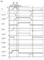
図6は、電力変換装置1の逆変換動作時におけるスイッチング素子Q1~Q4のオンオフ制御を説明するための動作波形図である。図6には、スイッチング素子Q1~Q4の各々の動作波形と、ノードab間の電圧Vabの動作波形が示されている。
FIG. 6 is an operation waveform diagram for explaining on/off control of the switching elements Q1 to Q4 during the reverse conversion operation of the
図6を参照して、電力変換装置1の制御回路5(図1)は、周期的な搬送波CW(三角波またはのこぎり波)の電圧と、正弦波信号V*(変調波)の電圧とを比較し、比較結果に基づいて、スイッチング素子Q1,Q2に対してゲート信号G1,G2をそれぞれ出力する。搬送波CWは、正弦波信号V*の極性に応じて2種類用意される。
Referring to FIG. 6, control circuit 5 (FIG. 1) of
具体的には、正弦波信号V*の電位が搬送波CWの電位よりも高いときには、スイッチング素子Q1がオンされ、スイッチング素子Q2がオフされる。一方、正弦波信号V*の電位が搬送波CWの電位よりも低いときには、スイッチング素子Q1がオフされ、スイッチング素子Q2がオンされる。すなわち、スイッチング素子Q1,Q2は、搬送波CWの周波数(以下、キャリア周波数とも称する)でオンオフが制御される。 Specifically, when the potential of the sine wave signal V* is higher than the potential of the carrier wave CW, the switching element Q1 is turned on and the switching element Q2 is turned off. On the other hand, when the potential of the sine wave signal V* is lower than the potential of the carrier wave CW, the switching element Q1 is turned off and the switching element Q2 is turned on. That is, the switching elements Q1 and Q2 are controlled to be turned on and off by the frequency of the carrier wave CW (hereinafter also referred to as carrier frequency).
これに対して、スイッチング素子Q3,Q4は、正弦波信号V*の周波数でオンオフが制御される。具体的には、正弦波信号V*の電圧が正となる期間では、スイッチング素子Q3がオフに固定され、スイッチング素子Q4がオンに固定される。正弦波信号V*の電圧が負となる期間では、スイッチング素子Q3がオンに固定され、スイッチング素子Q4がオフに固定される。 On the other hand, the switching elements Q3 and Q4 are controlled to be turned on and off at the frequency of the sine wave signal V*. Specifically, during a period in which the voltage of the sine wave signal V* is positive, the switching element Q3 is fixed off and the switching element Q4 is fixed on. During the period when the voltage of the sine wave signal V* is negative, the switching element Q3 is fixed on and the switching element Q4 is fixed off.
このように、本実施の形態1に係る電力変換装置においては、第1ハーフブリッジ回路A(スイッチング素子Q1,Q2)をキャリア周波数でオンオフさせるとともに、第2ハーフブリッジ回路B(スイッチング素子Q3,Q4)を交流電力の周波数でオンオフさせる。このような駆動方式は、「非対称駆動方式」とも呼ばれる。 Thus, in the power converter according to the first embodiment, the first half bridge circuit A (switching elements Q1, Q2) is turned on and off at the carrier frequency, and the second half bridge circuit B (switching elements Q3, Q4) is turned on and off at the carrier frequency. ) is switched on and off at the frequency of the AC power. Such a drive scheme is also called an "asymmetric drive scheme".
ここで、電力変換装置の駆動方式には、非対称駆動方式以外に、第1ハーフブリッジ回路Aおよび第2ハーフブリッジ回路Bの双方をキャリア周波数でオンオフさせる方式がある。このような駆動方式は「対称駆動方式」とも呼ばれる。図7および図8を用いて、対称駆動方式での逆変換動作について説明する。 In addition to the asymmetric driving method, the driving method of the power converter includes a method in which both the first half bridge circuit A and the second half bridge circuit B are turned on and off at the carrier frequency. Such a drive scheme is also called a "symmetrical drive scheme". The inverse conversion operation in the symmetrical driving method will be described with reference to FIGS. 7 and 8. FIG.
最初に、スイッチング素子Q1およびQ4をオンすると、図7(A)に示す回路状態となる。ノードaの電位Va=Vdcになり、ノードbの電位Vb=0になるので、リアクトルL1に電圧VL=Va-Vout-Vb=Vdc-Voutが加わり、図中の矢印で示すように、正の電流が次第に増加する形で流れる。 First, when the switching elements Q1 and Q4 are turned on, the circuit state shown in FIG. 7A is obtained. Since the potential of node a becomes Va=Vdc and the potential of node b becomes Vb=0, the voltage VL=Va−Vout−Vb=Vdc−Vout is applied to reactor L1, and as indicated by the arrow in the figure, a positive voltage is applied. The current flows in an increasing fashion.
次に、スイッチング素子Q1をオフし、スイッチング素子Q2をオンすると、すなわちスイッチング素子Q2およびQ4をオンすると、図7(B)に示す回路状態となる。リアクトルL1を通過している電流は、リアクトルの電流維持作用のため即時0になれず、正の方向に流れ続ける。リアクトルL1および負荷2の直列回路は短絡され、電圧Vab=0となるため、リアクトルL1に電圧VL=-Voutが加わり、電流は次第に減少する。
Next, when the switching element Q1 is turned off and the switching element Q2 is turned on, that is, when the switching elements Q2 and Q4 are turned on, the circuit state shown in FIG. 7B is obtained. The current passing through the reactor L1 cannot immediately become 0 due to the current maintenance action of the reactor, and continues to flow in the positive direction. Since the series circuit of reactor L1 and
次に、スイッチング素子Q1をオンし、スイッチング素子Q2をオフすると、すなわちスイッチング素子Q1およびQ4をオンすると、図7(C)に示す回路状態である。ノードaの電位Va=Vdcになり、ノードbの電位Vb=0になるので、リアクトルL1に電圧VL=Va-Vout-Vb=Vdc-Voutが加わり、図中の矢印で示すように、正の電流が次第に増加する形で流れる。 Next, when the switching element Q1 is turned on and the switching element Q2 is turned off, that is, when the switching elements Q1 and Q4 are turned on, the circuit state shown in FIG. 7(C) is obtained. Since the potential of node a becomes Va=Vdc and the potential of node b becomes Vb=0, the voltage VL=Va−Vout−Vb=Vdc−Vout is applied to reactor L1, and as indicated by the arrow in the figure, a positive voltage is applied. The current flows in an increasing fashion.
次に、スイッチング素子Q3をオンし、スイッチング素子Q4をオフすると、すなわちスイッチング素子Q1およびQ3をオンすると、図7(D)に示す回路状態となる。リアクトルL1を通過している電流は、リアクトルの電流維持作用のため即時0になれず、正の方向に流れ続ける。リアクトルL1および負荷2の直列回路は短絡され、電圧Vab=0となるため、リアクトルL1に電圧VL=-Voutが加わり、電流は次第に減少する。
Next, when the switching element Q3 is turned on and the switching element Q4 is turned off, that is, when the switching elements Q1 and Q3 are turned on, the circuit state shown in FIG. 7(D) is obtained. The current passing through the reactor L1 cannot immediately become 0 due to the current maintenance action of the reactor, and continues to flow in the positive direction. Since the series circuit of reactor L1 and
図7(A)~(D)の回路状態が繰り返されることにより、負荷2には正の電圧が印加されることとなる。スイッチング素子Q1,Q2をオンオフするスイッチング周期およびスイッチング素子Q3,Q4をオンオフするスイッチング周期は互いに等しい。
A positive voltage is applied to the
次に、スイッチング素子Q2およびQ3をオンすると、図8(A)に示す回路状態となる。ノードbの電位Vb=Vdcになり、ノードaの電位Va=0なるので、リアクトルL1に電圧VL=Va-Vout-Vb=-Vdc-Voutが加わり、図中の矢印で示すように、負の電流が、絶対値が次第に増加する形で流れる。 Next, when the switching elements Q2 and Q3 are turned on, the circuit state shown in FIG. 8(A) is obtained. Since the potential of the node b becomes Vb=Vdc and the potential of the node a becomes Va=0, the voltage VL=Va-Vout-Vb=-Vdc-Vout is applied to the reactor L1, and as indicated by the arrow in the figure, a negative voltage is applied. A current flows with increasing absolute value.
次に、スイッチング素子Q3をオフし、スイッチング素子Q4をオンすると、すなわちスイッチング素子Q2およびQ4をオンすると、図8(B)に示す回路状態となる。リアクトルL1を通過している電流は、電流維持作用のため即時0になれず、負の方向に流れ続ける。リアクトルL1および負荷2の直列回路は短絡され、電圧Vab=0となるため、リアクトルL1に電圧VL=-Voutが加わり、電流の絶対値は次第に減少する。
Next, when the switching element Q3 is turned off and the switching element Q4 is turned on, that is, when the switching elements Q2 and Q4 are turned on, the circuit state shown in FIG. 8B is obtained. The current passing through the reactor L1 cannot immediately become 0 due to the current maintenance action, and continues to flow in the negative direction. Since the series circuit of reactor L1 and
次に、スイッチング素子Q3をオンし、スイッチング素子Q4をオフすると、すなわちスイッチング素子Q2およびQ3をオンすると、図8(C)に示す回路状態となる。ノードbの電位Vb=Vdcになり、ノードaの電位Va=0なるので、リアクトルL1に電圧VL=Va-Vout-Vb=-Vdc-Voutが加わり、図中の矢印で示すように、負の電流が、絶対値が次第に増加する形で流れる。 Next, when the switching element Q3 is turned on and the switching element Q4 is turned off, that is, when the switching elements Q2 and Q3 are turned on, the circuit state shown in FIG. 8(C) is obtained. Since the potential of the node b becomes Vb=Vdc and the potential of the node a becomes Va=0, the voltage VL=Va-Vout-Vb=-Vdc-Vout is applied to the reactor L1, and as indicated by the arrow in the figure, a negative voltage is applied. A current flows with increasing absolute value.
次に、スイッチング素子Q1をオンし、スイッチング素子Q2をオフすると、すなわちスイッチング素子Q1およびQ3をオンすると、図8(D)に示す回路状態となる。リアクトルL1を通過している電流は、電流維持作用のため即時0になれず、負の方向に流れ続ける。リアクトルL1および負荷2の直列回路は短絡され、電圧Vab=0となるため、リアクトルL1に電圧VL=-Voutが加わり、電流の絶対値は次第に減少する。
Next, when the switching element Q1 is turned on and the switching element Q2 is turned off, that is, when the switching elements Q1 and Q3 are turned on, the circuit state shown in FIG. 8(D) is obtained. The current passing through the reactor L1 cannot immediately become 0 due to the current maintenance action, and continues to flow in the negative direction. Since the series circuit of reactor L1 and
図8(A)~(D)の回路状態が繰り返されることにおり、負荷2には負の電圧が印加されることとなる。スイッチング素子Q1,Q2をオンオフするスイッチング周期およびスイッチング素子Q3,Q4をオンオフするスイッチング周期は互いに等しい。
Since the circuit states of FIGS. 8A to 8D are repeated, a negative voltage is applied to the
図9は、対称駆動方式におけるスイッチング素子Q1~Q4のオンオフ制御を説明するための動作波形図である。図9には、スイッチング素子Q1~Q4の各々の動作波形と、ノードab間の電圧Vabの動作波形が示されている。 FIG. 9 is an operation waveform diagram for explaining on/off control of the switching elements Q1 to Q4 in the symmetrical drive system. FIG. 9 shows the operation waveforms of each of switching elements Q1-Q4 and the operation waveform of voltage Vab between nodes ab.
図9を参照して、搬送波CWの電圧と、正弦波信号V*(変調波)の電圧とを比較し、比較結果に基づいて、スイッチング素子Q1,Q2に対してゲート信号G1,G2がそれぞれ出力される。また、搬送波CWの電圧と正弦波信号V*を反転した信号/V*の電圧とを比較し、比較結果に基づいて、スイッチング素子Q3,Q4に対してゲート信号G3,G4がそれぞれ出力される。 Referring to FIG. 9, the voltage of carrier wave CW and the voltage of sine wave signal V* (modulation wave) are compared. output. Also, the voltage of the carrier wave CW is compared with the voltage of the signal /V* obtained by inverting the sine wave signal V*, and based on the comparison result, gate signals G3 and G4 are output to the switching elements Q3 and Q4, respectively. .
具体的には、正弦波信号V*の電位が搬送波CWの電位よりも高いときには、スイッチング素子Q1がオンされ、スイッチング素子Q2がオフされる。一方、正弦波信号V*の電位が搬送波CWの電位よりも低いときには、スイッチング素子Q1がオフされ、スイッチング素子Q2がオンされる。すなわち、スイッチング素子Q1,Q2は、キャリア周波数でオンオフが制御される。 Specifically, when the potential of the sine wave signal V* is higher than the potential of the carrier wave CW, the switching element Q1 is turned on and the switching element Q2 is turned off. On the other hand, when the potential of the sine wave signal V* is lower than the potential of the carrier wave CW, the switching element Q1 is turned off and the switching element Q2 is turned on. That is, the switching elements Q1 and Q2 are controlled to be turned on and off by the carrier frequency.
反転信号/V*の電位が搬送波CWの電位よりも高いときには、スイッチング素子Q3がオンされ、スイッチング素子Q4がオフされる。一方、反転信号/V*の電位が搬送波CWの電位よりも低いときには、スイッチング素子Q3がオフされ、スイッチング素子Q4がオンされる。すなわち、スイッチング素子Q3,Q4は、キャリア周波数でオンオフが制御される。 When the potential of the inverted signal /V* is higher than the potential of the carrier wave CW, the switching element Q3 is turned on and the switching element Q4 is turned off. On the other hand, when the potential of the inverted signal /V* is lower than the potential of the carrier wave CW, the switching element Q3 is turned off and the switching element Q4 is turned on. That is, the switching elements Q3 and Q4 are controlled to be turned on and off by the carrier frequency.
図6の動作波形図と図9の動作波形図とを比較すると、非対称駆動方式では、2つのハーフブリッジ回路の一方(図6では第2ハーフブリッジ回路B)がキャリア周波数よりも低い交流周波数でオンオフするため、2つのハーフブリッジ回路がともにキャリア周波数でオンオフする対称駆動方式に比べて、一方のハーフブリッジ回路のスイッチング回数を減らすことができる。スイッチング回数の減少は、該ハーフブリッジ回路で生じるスイッチング損失の低減に繋がるため、最適な素子を使用することで、電力変換装置全体の電力変換効率の向上が期待できる。 Comparing the operating waveform diagram of FIG. 6 with the operating waveform diagram of FIG. 9, in the asymmetric driving method, one of the two half-bridge circuits (the second half-bridge circuit B in FIG. 6) operates at an AC frequency lower than the carrier frequency. Since it turns on and off, it is possible to reduce the number of switching times of one half-bridge circuit compared to a symmetrical drive system in which both half-bridge circuits turn on and off at the carrier frequency. A reduction in the number of times of switching leads to a reduction in switching loss that occurs in the half-bridge circuit. Therefore, by using optimum elements, an improvement in the power conversion efficiency of the entire power converter can be expected.
非対称駆動方式では、さらに、ハーフブリッジ回路のスイッチング周波数に応じて、ハーフブリッジ回路を構成するスイッチング素子を使い分けることができる。 In the asymmetric driving method, switching elements constituting the half-bridge circuit can be selectively used according to the switching frequency of the half-bridge circuit.
例えば、スイッチング周波数がキャリア周波数であるハーフブリッジ回路(第1ハーフブリッジ回路A)については、高周波動作が可能なワイドバンドギャップ半導体材料(例えば、SiC(炭化珪素)、GaN(窒化ガリウム)など)を用いて形成されたスイッチング素子(例えばSiC-MOSFET、GaN-HEMTなど)を使用することができる。 For example, for a half-bridge circuit (first half-bridge circuit A) whose switching frequency is the carrier frequency, a wide bandgap semiconductor material capable of high-frequency operation (for example, SiC (silicon carbide), GaN (gallium nitride), etc.) is used. A switching element (eg, SiC-MOSFET, GaN-HEMT, etc.) formed by using a silicon oxide can be used.
電力変換動作においては、スイッチング素子のチャネルだけでなく、フリーホイールダイオードを通しても電流を流すモードが存在する。フリーホイールダイオードに電流を流したり、遮断したりする場合、逆回復現象により、瞬間的にダイオードの逆方向に電流が流れる。この逆方向に電流が流れる時間が長くなるほど、該時間に発生する損失が大きくなる。したがって、スイッチング周波数がキャリア周波数であるスイッチング素子は、逆回復時間が早いフリーホイールダイオード(ボディダイオードを含む)を有することが望ましい。好ましくは、逆回復時間は200ns以下である。例えば、IGBTに対して、SiCショットキーバリアダイオードまたはFRD(First Recovery Diode)を逆並列に接続することができる。あるいは、高速ボディダイオードタイプのMOSFETを使用することができる。 In power conversion operation, there is a mode in which current flows not only through the channel of the switching element but also through the freewheel diode. When the freewheeling diode is turned on or off, current instantaneously flows in the reverse direction of the diode due to the reverse recovery phenomenon. The longer the time for the current to flow in the opposite direction, the greater the loss that occurs during that time. Therefore, the switching element whose switching frequency is the carrier frequency preferably has a freewheeling diode (including a body diode) with a fast reverse recovery time. Preferably, the reverse recovery time is 200 ns or less. For example, a SiC Schottky barrier diode or FRD (First Recovery Diode) can be connected in anti-parallel to the IGBT. Alternatively, a fast body diode type MOSFET can be used.
これに対して、スイッチング周波数が交流電力の周波数であるハーフブリッジ回路(第2ハーフブリッジ回路B)については、プレーナタイプのSiMOSFETに比べて、高耐圧を確保しながら導通損失を低減することができる、Siスーパージャンクション(Super Junction)MOSFETを使用することができる。 On the other hand, the half-bridge circuit (second half-bridge circuit B) whose switching frequency is the frequency of AC power can reduce the conduction loss while ensuring a high withstand voltage compared to the planar type SiMOSFET. , Si Super Junction MOSFETs can be used.
さらに、非対称駆動方式を採用することで、交流電力の周波数でスイッチングするハーフブリッジ回路(第2ハーフブリッジ回路B)のスイッチング損失を低減できるため、キャリア周波数でスイッチングするハーフブリッジ回路(第1ハーフブリッジ回路A)にのみ補助共振回路を設けることで、スイッチング素子のソフトスイッチングを実現することができる。これにより、簡易な構成でソフトスイッチングを実行できるため、電力変換装置の高効率化および低ノイズ化を実現することができる。 Furthermore, by adopting the asymmetric drive method, the switching loss of the half bridge circuit (second half bridge circuit B) that switches at the frequency of the AC power can be reduced, so the half bridge circuit (first half bridge circuit B) that switches at the carrier frequency can be reduced. By providing the auxiliary resonant circuit only in the circuit A), soft switching of the switching element can be realized. As a result, since soft switching can be performed with a simple configuration, it is possible to achieve high efficiency and low noise of the power converter.
[実施の形態2]
以下の実施の形態2~5では、実施の形態1で説明した非対称駆動方式の電力変換装置1において、ソフトスイッチングを実現するための構成について説明する。
[Embodiment 2]
In the following second to fifth embodiments, configurations for realizing soft switching in the asymmetric drive
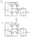
図10は、この発明の実施の形態2に従う電力変換装置1の主回路構成図である。図10を参照して、実施の形態2に従う電力変換装置1の回路構成は、図1に示した電力変換装置1の回路構成と基本的に同様であり、補助共振回路4および補助キャパシタCr1,Cr2を備える点が異なる。
FIG. 10 is a main circuit configuration diagram of
補助キャパシタCr1は、スイッチング素子Q1に並列に接続される。補助キャパシタCr2は、スイッチング素子Q2に並列に接続される。補助キャパシタCr1,Cr2としては、外付けのキャパシタを用いてもよいし、回路構成上等価な位置にあるスイッチング素子の寄生容量を用いてもよい。 Auxiliary capacitor Cr1 is connected in parallel with switching element Q1. Auxiliary capacitor Cr2 is connected in parallel with switching element Q2. As the auxiliary capacitors Cr1 and Cr2, external capacitors may be used, or parasitic capacitances of switching elements at equivalent positions in circuit configuration may be used.
補助共振回路4は、キャパシタCp,Cnと、補助スイッチング素子Qr1,Qr2と、補助リアクトルLrとを含む。キャパシタCpおよびCnは、同容量であり、直流端子T1(直流正母線PL1)および直流端子T2(直流負母線NL1)の間に直列に接続される。キャパシタCp,Cnは、直流電源P1の電圧V1を2分割するためのキャパシタである。キャパシタCp,Cnには、一般的に、電圧の変動を安定させるべく、容量が大きい電解キャパシタが用いられる。
補助スイッチング素子Qr1およびQr2は、キャパシタCpおよびCnの接続点(ノードn)とノードaとの間に電気的に直列に接続される。補助スイッチング素子Qr1,Qr2のオンオフは、制御回路5から出力されるゲート信号Gr1,Gr2によってそれぞれ制御される。なお、図10では、補助スイッチング素子Qr1,Qr2として、MOSFETを用いているが、IGBTなどの任意の自己消弧型のスイッチング素子を用いることができる。補助スイッチング素子Qr1,Qr2にはそれぞれ、補助ダイオードDr1,Dr2が逆並列に接続されている。補助スイッチング素子Qr1,Qr2および補助ダイオードDr1,Dr2は「双方向スイッチ」の一実施例に対応する。
Auxiliary switching elements Qr1 and Qr2 are electrically connected in series between a connection point (node n) of capacitors Cp and Cn and node a. On/off of the auxiliary switching elements Qr1 and Qr2 are controlled by gate signals Gr1 and Gr2 output from the
補助リアクトルLrは、補助スイッチング素子Qr1およびQr2の直列回路とノードaとの間に電気的に接続される。 Auxiliary reactor Lr is electrically connected between a series circuit of auxiliary switching elements Qr1 and Qr2 and node a.
次に、図11から図13を用いて、実施の形態2に従う電力変換装置1の動作、特に補助共振回路4によるソフトスイッチングを説明する。ここでは、負荷2に正の電圧を印加するとき(図2参照)のソフトスイッチングについて説明する。
Next, the operation of
以下の説明では、図10の補助スイッチング素子Qr1およびQr2の直列回路を補助スイッチSrで置き換えることとする。直流電源P1の出力電圧(電源電圧)をVdcとする。Ioは負荷2に流れる電流を示し、IL1はリアクトルL1に流れる電流を示し、ILrは補助リアクトルLrに流れるリアクトル電流を示す。
In the following description, the series circuit of auxiliary switching elements Qr1 and Qr2 in FIG. 10 is replaced with an auxiliary switch Sr. Let Vdc be the output voltage (power supply voltage) of the DC power supply P1. Io indicates the current flowing through the
図11および図12は、スイッチング素子Q2のダイオードD2に電流IL1が流れている状態(モードM0)からスイッチング素子Q1へ転流するときの状態を示している。図12は、図11に示す動作が実行された場合の動作波形図である。 FIGS. 11 and 12 show the state when the current IL1 is commutated to the switching element Q1 from the state (mode M0) in which the current IL1 flows through the diode D2 of the switching element Q2. FIG. 12 is an operation waveform diagram when the operation shown in FIG. 11 is executed.
図11を参照して、スイッチング素子Q2およびQ4がオンの状態においては(モードM0)、リアクトルL1および負荷2の直列回路が短絡され、図中の矢印で示すように、正の電流IL1が次第に減少する形で流れる。
Referring to FIG. 11, when switching elements Q2 and Q4 are on (mode M0), the series circuit of reactor L1 and
この状態で補助スイッチSr(補助スイッチング素子Qr1)のをターンオンすると(モードM1)、補助リアクトルLrに、正の電流ILrが流れ始める。転流期間中の電流ILrを一定とすれば、図13に示すように、リアクトル電流ILrはVdc/2Lrの傾きで直線的に増加し始める。 When the auxiliary switch Sr (auxiliary switching element Qr1) is turned on in this state (mode M1), a positive current ILr begins to flow through the auxiliary reactor Lr. If the current ILr during the commutation period is constant, the reactor current ILr begins to increase linearly with a slope of Vdc/2Lr, as shown in FIG.
リアクトル電流ILrが電流IL1よりも大きくなると、その超過分の電流は補助リアクトルLrからスイッチング素子Q2に流れ込み、キャパシタCp,Cnおよび補助スイッチSrを介して補助リアクトルLrに帰還する(モードM2)。 When reactor current ILr becomes larger than current IL1, the excess current flows from auxiliary reactor Lr into switching element Q2 and is fed back to auxiliary reactor Lr via capacitors Cp, Cn and auxiliary switch Sr (mode M2).
スイッチング素子Q2のドレイン電流Idが正になったときに、スイッチング素子Q2をターンオフすると(モードM3)、補助リアクトルLrと補助キャパシタCr1,Cr2とが共振動作になるため、リアクトル電流ILrはピーク値を向かえた後0に向かって減少する。このとき、リアクトル電流ILrは補助キャパシタCr1に流れ込むとともに、補助キャパシタCr2に流れ込む。この電流によって補助キャパシタCr2が充電され、かつ、補助キャパシタCr1が放電されることによって、スイッチング素子Q1およびQ2の接続点(ノードa)の電位が上昇する。このため、図13に示すように、スイッチング素子Q1のドレイン・ソース間電圧Vdsは次第に減少する。 When the switching element Q2 is turned off when the drain current Id of the switching element Q2 becomes positive (mode M3), the auxiliary reactor Lr and the auxiliary capacitors Cr1 and Cr2 operate in resonance, and the reactor current ILr reaches its peak value. Decrease toward 0 after turning. At this time, reactor current ILr flows into auxiliary capacitor Cr1 and auxiliary capacitor Cr2. This current charges auxiliary capacitor Cr2 and discharges auxiliary capacitor Cr1, thereby increasing the potential at the connection point (node a) between switching elements Q1 and Q2. Therefore, as shown in FIG. 13, the drain-source voltage Vds of the switching element Q1 gradually decreases.
ノードaの電位Va=Vdcに達すると、スイッチング素子Q1のダイオードD1がオンする。このダイオードD1がオンしている期間にスイッチング素子Q1をターンオンさせれば、ゼロ電圧スイッチングが行なわれることになる(モードM4)。 When the potential Va of the node a reaches Vdc, the diode D1 of the switching element Q1 is turned on. If the switching element Q1 is turned on while the diode D1 is on, zero voltage switching is performed (mode M4).
スイッチング素子Q1をターンオンすることにより、電流が直流電源P1の正極端子からスイッチング素子Q1に流れ込み、リアクトルL1、負荷2およびスイッチング素子Q4を介して直流電源P1の負極端子に帰還する(モードM5)。スイッチング素子Q1のドレイン・ソース間に流れるドレイン電流Idが次第に増加し、それに伴ってリアクトル電流ILrが減少する。リアクトル電流ILr=0となった後に、補助スイッチSr(補助スイッチング素子Qr1)をオフする(モードM6)。補助スイッチング素子Qr2の補助ダイオードDr2により負の電流は流れない。
By turning on switching element Q1, current flows from the positive terminal of DC power supply P1 to switching element Q1, and returns to the negative terminal of DC power supply P1 via reactor L1,
図14に、スイッチング素子Q1のドレイン・ソース間電圧Vdsおよびドレイン電流Idの動作波形の周波数スペクトルを示す。図14(A)には、実施の形態1に従う電力変換装置1(補助共振回路無し)のスイッチング素子Q1のVds波形の周波数スペクトル(波形k1)および、実施の形態2に従う電力変換装置1(補助共振回路有り)のスイッチング素子Q1のVds波形の周波数スペクトル(波形k2)が示されている。
FIG. 14 shows frequency spectra of operating waveforms of the drain-source voltage Vds and the drain current Id of the switching element Q1. FIG. 14A shows the frequency spectrum (waveform k1) of the Vds waveform of switching element Q1 of power converter 1 (without auxiliary resonance circuit) according to
図14(B)には、実施の形態1に従う電力変換装置1のスイッチング素子Q1のId波形の周波数スペクトル(波形k3)および、実施の形態2に従う電力変換装置1のスイッチング素子Q1のId波形の周波数スペクトル(波形k4)が示されている。
FIG. 14B shows the frequency spectrum (waveform k3) of the Id waveform of switching element Q1 of
図14(A)に示されるように、補助共振回路4を利用してスイッチング素子Q1をソフトスイッチングしたことにより、スイッチング素子Q1をハードスイッチングした場合に比べて、Vdsの高周波領域での強度が小さくなっている。図14(B)においても、スイッチング素子Q1をソフトスイッチングしたことにより、スイッチング素子Q1をハードスイッチングした場合に比べて、Idの高周波領域での強度が小さくなっている。このように、第1ハーフブリッジ回路Aのスイッチング素子をソフトスイッチングすることで、電磁干渉(EMI)ノイズを低減することができる。
As shown in FIG. 14A, by soft-switching the switching element Q1 using the
以上説明したように、実施の形態2に従う電力変換装置によれば、フルブリッジ回路において、キャリア周波数でスイッチングするハーフブリッジ回路にのみ補助共振回路を設けることによって、簡易な構成でスイッチング損失の低減およびEMIノイズの低減を実現することができる。 As described above, according to the power converter according to the second embodiment, in the full bridge circuit, by providing the auxiliary resonance circuit only in the half bridge circuit that switches at the carrier frequency, the switching loss can be reduced and the switching loss can be reduced with a simple configuration. A reduction in EMI noise can be achieved.
[実施の形態3]
上述した実施の形態2に従う電力変換装置1においては、補助共振回路4には、直流電源P1の電圧Vdcを2分割して中点電位(Vdc/2)を生成するためにキャパシタCp,Crの直列回路を用いている。そのため、負荷の大きさなどによって中点電位が変動する場合がある。また、キャパシタCp,Crに電解キャパシタを用いた場合、電解キャパシタは温度上昇によって容量が低下する電気部品であるため、キャパシタCp,Cnの劣化が進行することで、電力変換装置全体の寿命が短くなることが懸念される。
[Embodiment 3]
In
以下、実施の形態3~5では、キャパシタCp,Crの直列回路を用いずにスイッチング素子Q1,Q2のソフトスイッチングを実現するための補助共振回路の新たな構成について説明する。 In third to fifth embodiments, new configurations of auxiliary resonance circuits for realizing soft switching of switching elements Q1 and Q2 without using a series circuit of capacitors Cp and Cr will be described below.
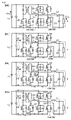
図15は、この発明の実施の形態3に従う電力変換装置1の主回路構成図である。図15を参照して、実施の形態3に従う電力変換装置1は、補助共振回路4Aの構成が図10に示した実施の形態2に従う電力変換装置1の補助共振回路4の構成と異なる。その他の点については、実施の形態2と共通するので、同一または相当する部分には同一の参照符号を付して説明は繰返さない。
FIG. 15 is a main circuit configuration diagram of
補助共振回路4Aは、補助スイッチング素子Qr1,Qr2および補助リアクトルLrを含む。補助スイッチング素子Qr1およびQr2は、直流端子T1(直流正母線PL1)および直流端子T2(直流負母線NL1)の間に電気的に直列に接続される。補助リアクトルLrは、補助スイッチング素子Qr1およびQr2の接続点(ノードc)とノードaとの間に電気的に接続される。
Auxiliary
次に、図16から図19を用いて、実施の形態3に従う電力変換装置1の動作、特に補助共振回路4Aによるソフトスイッチングを説明する。図16および図17では、負荷2に正の電圧を印加するときのソフトスイッチングについて説明する。
Next, the operation of
図16は、スイッチング素子Q2のダイオードD2に電流IL1が流れている状態(モードM0)からスイッチング素子Q1へ転流するときの状態を示している。図17は、図16に示す動作が実行された場合の動作波形図である。 FIG. 16 shows a state in which the current IL1 flows through the diode D2 of the switching element Q2 (mode M0) and is commutated to the switching element Q1. FIG. 17 is an operation waveform diagram when the operation shown in FIG. 16 is executed.
図16を参照して、スイッチング素子Q2およびQ4がオンの状態においては(モードM0)、リアクトルL1および負荷2の直列回路が短絡され、図中の矢印で示すように、正の電流IL1が次第に減少する形で流れる。
Referring to FIG. 16, when switching elements Q2 and Q4 are on (mode M0), the series circuit of reactor L1 and
この状態で補助スイッチング素子Qr1をターンオンすると(モードM1)、補助リアクトルLrに、正のリアクトル電流ILrが流れ始める。リアクトル電流ILrは、直流電源P1の正極端子から補助スイッチSr1、補助リアクトルLr、リアクトルL1、負荷2、スイッチング素子Q4を介して直流電源P1の負極端子に帰還される。転流期間中の電流IL1を一定とすれば、図17に示すように、リアクトル電流ILrはVdc/Lrの傾きで直線的に増加し始める。
When auxiliary switching element Qr1 is turned on in this state (mode M1), positive reactor current ILr begins to flow through auxiliary reactor Lr. Reactor current ILr is fed back from the positive terminal of DC power supply P1 to the negative terminal of DC power supply P1 via auxiliary switch Sr1, auxiliary reactor Lr, reactor L1,
リアクトル電流ILrが電流IL1よりも大きくなると、その超過分は補助リアクトルLrからスイッチング素子Q2に流れ込む。スイッチング素子Q2のドレイン電流Idが正になったときに、スイッチング素子Q2をターンオフすると(モードM2)、補助リアクトルLrと補助キャパシタCr1,Cr2とが共振動作になる。このとき、リアクトル電流ILrは補助キャパシタCr1に流れ込むとともに、補助キャパシタCr2に流れ込む。この電流によって補助キャパシタCr2が充電され、かつ、補助キャパシタCr1が放電されることによって、スイッチング素子Q1およびQ2の接続点(ノードa)の電位が上昇する。このため、図17に示すように、スイッチング素子Q1のドレイン・ソース間電圧Vdsは次第に減少する。 When reactor current ILr becomes larger than current IL1, the excess flows from auxiliary reactor Lr into switching element Q2. When the switching element Q2 is turned off when the drain current Id of the switching element Q2 becomes positive (mode M2), the auxiliary reactor Lr and the auxiliary capacitors Cr1 and Cr2 start resonant operation. At this time, reactor current ILr flows into auxiliary capacitor Cr1 and auxiliary capacitor Cr2. This current charges auxiliary capacitor Cr2 and discharges auxiliary capacitor Cr1, thereby increasing the potential at the connection point (node a) between switching elements Q1 and Q2. Therefore, as shown in FIG. 17, the drain-source voltage Vds of the switching element Q1 gradually decreases.
ノードaの電位Va=Vdcに達すると、スイッチング素子Q1のダイオードD1がオンする。このダイオードD1がオンしている期間にスイッチング素子Q1をターンオンさせれば、ゼロ電圧スイッチングが行なわれることになる(モードM3)。スイッチング素子Q1のターンオンと同じタイミングで、補助スイッチング素子Qr1をターンオフする。 When the potential Va of the node a reaches Vdc, the diode D1 of the switching element Q1 is turned on. If the switching element Q1 is turned on while the diode D1 is on, zero voltage switching is performed (mode M3). The auxiliary switching element Qr1 is turned off at the same timing as the switching element Q1 is turned on.
スイッチング素子Q1をターンオンすると(モードM3)、補助リアクトルLrの電流維持作用により、リアクトル電流ILrは、補助リアクトルLrからスイッチング素子Q1のダイオードD1、直流電源P1の正極端子、補助スイッチング素子Qr2の順に流れるとともに、補助リアクトルLrからリアクトルL1、負荷2、スイッチS4、補助スイッチング素子Qr2の補助ダイオードDr2の順に流れることとなる。図17に示すように、リアクトル電流ILrは直線的に減少し始める。
When the switching element Q1 is turned on (mode M3), due to the current maintenance action of the auxiliary reactor Lr, the reactor current ILr flows from the auxiliary reactor Lr through the diode D1 of the switching element Q1, the positive terminal of the DC power supply P1, and the auxiliary switching element Qr2 in that order. At the same time, the current flows from the auxiliary reactor Lr to the reactor L1, the
リアクトル電流ILrが減少し始めると、電流IL1を一定とするために、直流電源P1の正極端子からリアクトルL1に電流が流れ込み、負荷2、スイッチング素子Q4を介して直流電源P1の負極端子に帰還する(モードM4)。スイッチング素子Q1のドレイン・ソース間に流れるドレイン電流Idが次第に増加する。この状態でリアクトル電流ILr=0になると(モードM5)、ドレイン電流Idが一定となる。
When reactor current ILr begins to decrease, in order to keep current IL1 constant, current flows from the positive terminal of DC power supply P1 to reactor L1 and returns to the negative terminal of DC power supply P1 via
次に、図18および図19を用いて、負荷2に負の電圧を印加するときのソフトスイッチングについて説明する。
Next, soft switching when a negative voltage is applied to the
図18は、スイッチング素子Q1のダイオードD1に電流IL1が流れている状態(モードM0)からスイッチング素子Q2へ転流するときの状態を示している。図19は、図18に示す動作が実行された場合の動作波形図である。 FIG. 18 shows a state in which the current IL1 flows through the diode D1 of the switching element Q1 (mode M0) and is commutated to the switching element Q2. FIG. 19 is an operation waveform diagram when the operation shown in FIG. 18 is executed.
図18を参照して、スイッチング素子Q1およびQ3がオンの状態においては(モードM0)、リアクトルL1および負荷2の直列回路が短絡され、図中の矢印で示すように、負の電流IL1の絶対値が次第に減少する形で流れる。
Referring to FIG. 18, when switching elements Q1 and Q3 are on (mode M0), the series circuit of reactor L1 and
この状態で補助スイッチング素子Qr2をターンオンすると(モードM1)、補助リアクトルLrに、負のリアクトル電流ILrが流れ始める。リアクトル電流ILrは、直流電源P1の正極端子からスイッチング素子Q3、負荷2、リアクトルL1、補助リアクトルLr、補助スイッチング素子Qr2を介して直流電源P1の負極端子に帰還される。転流期間中の電流IL1を一定とすれば、図19に示すように、リアクトル電流ILrは直線的に減少し始める。
When auxiliary switching element Qr2 is turned on in this state (mode M1), negative reactor current ILr begins to flow through auxiliary reactor Lr. Reactor current ILr is fed back from the positive terminal of DC power supply P1 to the negative terminal of DC power supply P1 via switching element Q3,
この状態でスイッチング素子Q1をターンオフすると(モードM2)、補助リアクトルLrと補助キャパシタCr1,Cr2とが共振動作になる。このとき、リアクトル電流ILrは補助キャパシタCr1に流れ込むとともに、補助キャパシタCr2に流れ込む。この電流によって補助キャパシタCr2が放電され、かつ、補助キャパシタCr1が充電されることによって、スイッチング素子Q1およびQ2の接続点(ノードa)の電位が低下する。このため、図19に示すように、スイッチング素子Q2のドレイン・ソース間電圧Vdsは次第に減少する。 When the switching element Q1 is turned off in this state (mode M2), the auxiliary reactor Lr and the auxiliary capacitors Cr1 and Cr2 are brought into resonance operation. At this time, reactor current ILr flows into auxiliary capacitor Cr1 and auxiliary capacitor Cr2. This current discharges auxiliary capacitor Cr2 and charges auxiliary capacitor Cr1, thereby lowering the potential at the connection point (node a) between switching elements Q1 and Q2. Therefore, as shown in FIG. 19, the drain-source voltage Vds of the switching element Q2 gradually decreases.
ノードaの電位Va=0に達すると、スイッチング素子Q2のダイオードD2がオンする。このダイオードD2がオンしている期間にスイッチS2のスイッチング素子Q2をターンオンさせれば、ゼロ電圧スイッチングが行なわれることになる(モードM3)。スイッチング素子Q2のターンオンと同じタイミングで、補助スイッチング素子Qr2をターンオフする。
When the potential Va of the node a
補助スイッチング素子Qr2がターンオフすると(モードM3)、補助リアクトルLrの電流維持作用により、リアクトル電流ILrは、補助リアクトルLrから補助スイッチング素子Qr1のダイオードDr1を介して直流電源P1の正極端子、負極端子、スイッチング素子Q2のダイオードD2の順に流れるとともに、補助リアクトルLrからスイッチング素子Q3、負荷2、リアクトルL1の順に流れることとなる。図19に示すように、リアクトル電流ILrは直線的に増加し始める。
When the auxiliary switching element Qr2 is turned off (mode M3), due to the current maintenance action of the auxiliary reactor Lr, the reactor current ILr flows from the auxiliary reactor Lr through the diode Dr1 of the auxiliary switching element Qr1 to the positive and negative terminals of the DC power supply P1. The current flows through the diode D2 of the switching element Q2 in this order, and also flows from the auxiliary reactor Lr through the switching element Q3, the
リアクトル電流ILrが増加し始めると、電流IL1を一定とするために、直流電源P1の正極端子からスイッチング素子Q3および負荷2を介してリアクトルL1に電流が流れ込み、スイッチング素子Q2を介して直流電源P1の負極端子に帰還する(モードM4)。スイッチング素子Q3のドレイン・ソース間に流れるドレイン電流Idが次第に増加する。この状態でリアクトル電流ILrが0になると(モードM5)、ドレイン電流Idが一定となる。
When reactor current ILr starts to increase, in order to keep current IL1 constant, current flows from the positive terminal of DC power supply P1 through switching element Q3 and
以上説明したように、この発明の実施の形態3に従う電力変換装置1によれば、補助共振回路にキャパシタCp,Crの直列回路が含まれていないため、直列回路の中点電位の変動を抑制することができる。また、キャパシタCp,Crの劣化に起因した電力変換装置の寿命の低下を防ぐことができる。
As described above, according to the
[実施の形態4]
上述した実施の形態3に従う補助共振回路4Aにおいては、補助リアクトルLrと補助キャパシタCr1,Cr2との共振動作により、補助スイッチング素子Qr1に電流が流れている状態(図16のモードM2)において、補助スイッチング素子Qr1をターンオフさせている(モードM3)。そのため、半導体スイッチング素子Q1をソフトスイッチングできる一方で、補助スイッチング素子Qr1がハードスイッチングになることが懸念される。
[Embodiment 4]
In the auxiliary
補助スイッチング素子Qr1,Qr2をソフトスイッチングするためには、実施の形態2で示したように、直流電源P1の電圧Vdcを2分割した電圧を作ることが必要になるが、上記の理由からキャパシタCp,Cnの直列回路を用いることは得策ではない。 In order to soft-switch the auxiliary switching elements Qr1 and Qr2, it is necessary to create a voltage obtained by dividing the voltage Vdc of the DC power supply P1 into two as shown in the second embodiment. , Cn in series is not advisable.
以下の実施の形態4および5では、キャパシタCp,Cnの直列回路を用いずに、直流電源P1の電圧Vdcを2分割した電圧を生成することができる補助共振回路の構成について説明する。 In the following fourth and fifth embodiments, configurations of auxiliary resonance circuits capable of generating a voltage obtained by dividing voltage Vdc of DC power supply P1 into two without using a series circuit of capacitors Cp and Cn will be described.
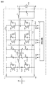
図20は、この発明の実施の形態4に従う電力変換装置1の主回路構成図である。図20を参照して、実施の形態4に従う電力変換装置1は、補助共振回路4Bの構成が図10に示した実施の形態2に従う電力変換装置1の補助共振回路4の構成と異なる。その他の点については、実施の形態2と共通するので、同一または相当する部分には同一の参照符号を付して説明は繰返さない。
FIG. 20 is a main circuit configuration diagram of
補助共振回路4Bは、補助スイッチング素子Qr1,Qr2、補助リアクトルLr、およびトランスTr1を含む。トランスTr1は、一次巻線n1および二次巻線n2を含む。トランスTr1は、理想トランスに加えて、励磁インダクタンスLmおよび漏れインダクタンスを有している。一次巻線n1と二次巻線n2とが電磁的に結合されることにより、一次巻線n1および二次巻線n2に同極性の起電力が誘起される。一次巻線n1と二次巻線n2との巻線比は2:1である。トランスTr1は「第1のトランス」の一実施例に対応する。
トランスTr1の一次巻線n1は、直流端子T1(直流正母線PL1)および直流端子T2(直流負母線NL1)の間に電気的に接続される。トランスTr1の二次巻線n2は、第1ハーフブリッジ回路Aのノードaおよび直流負母線NL1の間に電気的に接続される。 Primary winding n1 of transformer Tr1 is electrically connected between DC terminal T1 (DC positive bus PL1) and DC terminal T2 (DC negative bus NL1). A secondary winding n2 of transformer Tr1 is electrically connected between node a of first half bridge circuit A and DC negative bus NL1.
補助スイッチング素子Qr1は、トランスTr1の一次巻線n1および直流負母線NL1の間に電気的に接続される。補助スイッチング素子Qr2は、トランスTr1の二次巻線n2および直流負母線NL1の間に電気的に接続される。補助スイッチング素子Qr1,Qr2にはそれぞれ、補助ダイオードDr1,Dr2が逆並列に接続されている。 Auxiliary switching element Qr1 is electrically connected between primary winding n1 of transformer Tr1 and DC negative bus NL1. Auxiliary switching element Qr2 is electrically connected between secondary winding n2 of transformer Tr1 and DC negative bus NL1. Auxiliary diodes Dr1 and Dr2 are connected in antiparallel to the auxiliary switching elements Qr1 and Qr2, respectively.
補助リアクトルLrは、二次巻線n2およびノードaの間に接続される。補助リアクトルLrは、トランスTr1の漏れインダクタンスを利用してもよく、外付けしてもよい。 Auxiliary reactor Lr is connected between secondary winding n2 and node a. The auxiliary reactor Lr may utilize the leakage inductance of the transformer Tr1 or may be externally attached.
次に、図21から図26を用いて、実施の形態4に従う電力変換装置1の動作、特に補助共振回路4Bによるソフトスイッチングを説明する。図21から図23では、負荷2に正の電圧を印加するときのソフトスイッチングについて説明する。
Next, the operation of
図21および図22は、スイッチング素子Q2のダイオードD2に電流IL1が流れている状態(モードM0)からスイッチング素子Q1へ転流するときの状態を示している。図23は、図21および図22に示す動作が実行された場合の動作波形図である。 FIGS. 21 and 22 show the state when the current IL1 is commutated to the switching element Q1 from the state (mode M0) in which the current IL1 flows through the diode D2 of the switching element Q2. FIG. 23 is an operation waveform diagram when the operations shown in FIGS. 21 and 22 are executed.
図21を参照して、スイッチング素子Q2およびQ4がオンの状態においては(モードM0)、リアクトルL1および負荷2の直列回路が短絡され、図中の矢印で示すように、正の電流IL1が次第に減少する形で流れる。
Referring to FIG. 21, when switching elements Q2 and Q4 are on (mode M0), the series circuit of reactor L1 and
この状態で補助スイッチング素子Qr1をターンオンすると(モードM1)、トランスTr1の一次巻線n1には直流電源P1の電圧Vdcが印加され、一次巻線n1と二次巻線n2との巻線比が2:1であるので、二次巻線n2および補助リアクトルLrの接続点には電圧Vdcの1/2の電圧が印加される。これにより、補助リアクトルLrに、正のリアクトル電流ILrが流れ始める。リアクトル電流ILrは、トランスTr1の二次巻線n2から補助リアクトルLr、スイッチング素子Q4、補助スイッチング素子Qr2の補助ダイオードDr2を介して二次巻線n2に帰還される。転流期間中の電流IL1を一定とすれば、図23に示すように、リアクトル電流ILrはVdc/2Lrの傾きで直線的に増加し始める。また、スイッチング素子Q2のドレイン電流Idは0に向かって直線的に増加し始める。 When the auxiliary switching element Qr1 is turned on in this state (mode M1), the voltage Vdc of the DC power supply P1 is applied to the primary winding n1 of the transformer Tr1, and the turns ratio between the primary winding n1 and the secondary winding n2 becomes Since the ratio is 2:1, a voltage half the voltage Vdc is applied to the connection point between the secondary winding n2 and the auxiliary reactor Lr. As a result, the positive reactor current ILr begins to flow through the auxiliary reactor Lr. Reactor current ILr is fed back from secondary winding n2 of transformer Tr1 to secondary winding n2 via auxiliary reactor Lr, switching element Q4, and auxiliary diode Dr2 of auxiliary switching element Qr2. If the current IL1 during the commutation period is constant, the reactor current ILr begins to increase linearly with a slope of Vdc/2Lr, as shown in FIG. Also, the drain current Id of the switching element Q2 begins to increase linearly toward zero.
リアクトル電流ILrが電流IL1よりも大きくなると、その超過分の電流は補助リアクトルLrからスイッチング素子Q2に流れ込む(モードM2)。 When reactor current ILr becomes larger than current IL1, the excess current flows from auxiliary reactor Lr into switching element Q2 (mode M2).
スイッチング素子Q2のドレイン電流Idが正になったときに、スイッチング素子Q2をターンオフすると(モードM3)、補助リアクトルLrと補助キャパシタCr1,Cr2とが共振動作になる。このとき、リアクトル電流ILrは、補助キャパシタCr2に流れ込むとともに、補助キャパシタCr1に流れ込む。この電流によって補助キャパシタCr2が充電され、かつ、補助キャパシタCr1が放電されることによって、スイッチング素子Q1およびQ2の接続点(ノードa)の電位が上昇する。このため、図23に示すように、スイッチング素子Q1のドレイン・ソース間電圧Vdsは次第に減少する。 When the switching element Q2 is turned off when the drain current Id of the switching element Q2 becomes positive (mode M3), the auxiliary reactor Lr and the auxiliary capacitors Cr1 and Cr2 start resonant operation. At this time, reactor current ILr flows into auxiliary capacitor Cr2 and auxiliary capacitor Cr1. This current charges auxiliary capacitor Cr2 and discharges auxiliary capacitor Cr1, thereby increasing the potential at the connection point (node a) between switching elements Q1 and Q2. Therefore, as shown in FIG. 23, the drain-source voltage Vds of the switching element Q1 gradually decreases.
ノードaの電位Va=Vdcに達すると、スイッチング素子Q1のダイオードD1がオンする。このダイオードD1がオンしている期間にスイッチング素子Q1をターンオンさせれば、ゼロ電圧スイッチングが行なわれることになる(モードM4)。 When the potential Va of the node a reaches Vdc, the diode D1 of the switching element Q1 is turned on. If the switching element Q1 is turned on while the diode D1 is on, zero voltage switching is performed (mode M4).
スイッチング素子Q1をターンオンすると(モードM5)、電流が直流電源P1の正極端子からスイッチング素子Q1に流れ込み、リアクトルL1、負荷2、スイッチング素子Q4を介して直流電源P1の負極端子に帰還する。スイッチング素子Q1のドレイン・ソース間に流れるドレイン電流Idが次第に増加する。リアクトル電流ILr=0となったときに、補助スイッチング素子Qr1をターンオフすることにより(モードM6)、補助スイッチング素子Qr1のゼロ電流スイッチングが行なわれる。
When the switching element Q1 is turned on (mode M5), current flows from the positive terminal of the DC power supply P1 to the switching element Q1 and returns to the negative terminal of the DC power supply P1 via the reactor L1, the
次に、図24および図26を用いて、負荷2に負の電圧を印加するときのソフトスイッチングについて説明する。
Next, soft switching when a negative voltage is applied to the
図24および図25は、スイッチング素子Q1のダイオードD1に電流IL1が流れている状態(モードM0)からスイッチング素子Q2へ転流するときの状態を示している。図26は、図24および図25に示す動作が実行された場合の動作波形図である。 FIGS. 24 and 25 show the state when the current IL1 is commutated to the switching element Q2 from the state (mode M0) in which the current IL1 flows through the diode D1 of the switching element Q1. FIG. 26 is an operation waveform diagram when the operations shown in FIGS. 24 and 25 are executed.
図24を参照して、スイッチング素子Q1およびQ3がオンの状態においては(モードM0)、リアクトルL1および負荷2の直列回路が短絡され、図中の矢印で示すように、負の電流IL1の絶対値が次第に減少する形で流れる。
Referring to FIG. 24, when switching elements Q1 and Q3 are on (mode M0), the series circuit of reactor L1 and
この状態で補助スイッチング素子Qr2をターンオンすると(モードM1)、補助リアクトルLrに、負のリアクトル電流ILrが流れ始める。リアクトル電流ILrは、直流電源P1の正極端子からスイッチング素子Q3、負荷2、リアクトルL1、補助リアクトルLr、補助スイッチング素子Qr2を介して直流電源P1の負極端子に帰還される。このとき、補助ダイオードDr1、一次巻線n1、直流電源P1、補助ダイオードDr1の経路で電流が流れる。一次巻線n1には電圧Vdcが印加され、一次巻線nと二次巻線n2との巻線比が2:1であるので、二次巻線n2および補助リアクトルLrの接続点には電圧Vdcの1/2の電圧が印加される。転流期間中の電流IL1を一定とすれば、図26に示すように、リアクトル電流ILrは-Vdc/2Lrの傾きで直線的に減少し始める。また、スイッチング素子Q1のドレイン電流Idは0に向かって直線的に増加し始める。
When auxiliary switching element Qr2 is turned on in this state (mode M1), negative reactor current ILr begins to flow through auxiliary reactor Lr. Reactor current ILr is fed back from the positive terminal of DC power supply P1 to the negative terminal of DC power supply P1 via switching element Q3,
リアクトル電流ILrが電流IL1よりも小さくなると、その超過分の電流はスイッチング素子Q3に流れ込む(モードM2)。 When reactor current ILr becomes smaller than current IL1, the excess current flows into switching element Q3 (mode M2).
スイッチング素子Q1のドレイン電流Idが正になったときに、スイッチング素子Q1をターンオフすると(モードM3)、補助リアクトルLrと補助キャパシタCr1,Cr2とが共振動作になる。このとき、リアクトル電流ILrは、補助キャパシタCr2に流れ込むとともに、補助キャパシタCr1に流れ込む。この電流によって補助キャパシタCr1が充電され、かつ、補助キャパシタCr2が放電されることによって、スイッチング素子Q1およびQ2の接続点(ノードa)の電位が低下する。このため、図26に示すように、スイッチング素子Q2のドレイン・ソース間電圧Vdsは次第に減少する。 When the switching element Q1 is turned off when the drain current Id of the switching element Q1 becomes positive (mode M3), the auxiliary reactor Lr and the auxiliary capacitors Cr1 and Cr2 are in resonance operation. At this time, reactor current ILr flows into auxiliary capacitor Cr2 and auxiliary capacitor Cr1. This current charges auxiliary capacitor Cr1 and discharges auxiliary capacitor Cr2, thereby lowering the potential at the connection point (node a) between switching elements Q1 and Q2. Therefore, as shown in FIG. 26, the drain-source voltage Vds of the switching element Q2 gradually decreases.
ノードaの電位Va=0に達すると、スイッチング素子Q2のダイオードD2がオンする。このダイオードD2がオンしている期間にスイッチング素子Q2をターンオンさせれば、ゼロ電圧スイッチングが行なわれることになる(モードM4)。
When the potential Va of the node a
スイッチング素子Q2をターンオンすると、電流が直流電源P1の正極端子からスイッチング素子Q3に流れ込み、負荷2、リアクトルL1、スイッチング素子Q2を介して直流電源P1の負極端子に帰還する(モードM5)。スイッチング素子Q2のドレイン・ソース間に流れるドレイン電流Idが次第に増加する。リアクトル電流ILr=0となったときに、補助スイッチング素子Qr2をターンオフすることにより(モードM6)、補助スイッチング素子Qr1のゼロ電流スイッチングが行なわれる。
When switching element Q2 is turned on, current flows from the positive terminal of DC power supply P1 to switching element Q3 and returns to the negative terminal of DC power supply P1 via
以上説明したように、この発明の実施の形態4に従う電力変換装置1によれば、キャパシタCp,Cnの直列回路を用いずに、直流電源P1の電圧Vdcを2分割した電圧を生成することができるため、補助スイッチング素子Qr1,Qr2をソフトスイッチングすることができる。
As described above, according to
また、本実施の形態4に従う電力変換装置1において、補助スイッチング素子Qr1およびQr2はともに、直流電源P1の負極端子(直流負母線NL1)に接続されているため、補助スイッチング素子Qr1のゲート信号Gr1と、補助スイッチング素子Qr2のゲート信号Gr2とを同電位の信号とすることができる。図15に示した実施の形態3に従う電力変換装置1においては、補助スイッチング素子Qr1およびQr2が直流正母線PL1および直流負母線NL1の間に直列に接続されるため、高電位側の補助スイッチング素子Qr1のゲート信号Gr1の電位を、低電位側の補助スイッチング素子Qr1のゲート信号Gr2の電位よりも高くする必要がある。そのため、補助スイッチング素子Qr1のゲート駆動回路は、ゲート信号Gr1の電位を上げるためのレベルシフタが内蔵されており、補助スイッチング素子Qr2のゲート駆動回路とは電気的に分離されている。
Further, in
これに対して、本実施の形態4においては、補助スイッチング素子Qr1およびQr2が同電位にあるため、互いのゲート駆動回路を電気的に分離することが不要となる。したがって、ゲート駆動回路を簡素化でき、結果的に電力変換装置1を小型化および低コスト化することができる。
In contrast, in the fourth embodiment, since the auxiliary switching elements Qr1 and Qr2 are at the same potential, it is not necessary to electrically separate the gate drive circuits from each other. Therefore, the gate drive circuit can be simplified, and as a result, the size and cost of the
[変形例]
図27は、本実施の形態4の変形例に従う電力変換装置1の主回路構成図である。図27を参照して、実施の形態4の変形例に従う電力変換装置1は、補助共振回路4Cの構成が図20に示した実施の形態4に従う電力変換装置1の補助共振回路4Bの構成と異なる。その他の点については、実施の形態2と共通するので、同一または相当する部分には同一の参照符号を付して説明は繰返さない。
[Modification]
FIG. 27 is a main circuit configuration diagram of
本変形例に従う電力変換装置1においては、図20に示した電力変換装置1のトランスTr1がトランスTr2に置き換えられるとともに、ダイオードDa2が追加されている。
In
トランスTr2は、一次巻線n1、二次巻線n2およびリセット巻線n3を含む。リセット巻線n3は、一方端が直流正母線PLに接続され、他方端がダイオードDa2のカソードに接続されている。ダイオードDa2のアノードは直流負母線NL1に接続されている。すなわち、ダイオードDa2およびリセット巻線n3の直列回路は、直流負母線NL1から直流正母線PL1に向かう方向がダイオードDa2の順方向となるように、直流正母線PL1および直流負母線NL1の間に電気的に接続されている。 Transformer Tr2 includes a primary winding n1, a secondary winding n2 and a reset winding n3. Reset winding n3 has one end connected to DC positive bus PL and the other end connected to the cathode of diode Da2. The anode of diode Da2 is connected to DC negative bus NL1. That is, the series circuit of the diode Da2 and the reset winding n3 is electrically connected between the DC positive bus PL1 and the DC negative bus NL1 so that the direction from the DC negative bus NL1 to the DC positive bus PL1 is the forward direction of the diode Da2. properly connected.
リセット巻線n3およびダイオードDa2は、トランスTr2の励磁インダクタンスLmに蓄積された電磁エネルギを放出するためのリセット回路を構成する。 Reset winding n3 and diode Da2 form a reset circuit for releasing electromagnetic energy accumulated in exciting inductance Lm of transformer Tr2.
具体的には、補助スイッチング素子Qr1,Qr2がオフしたときには、トランスTr2の励磁インダクタンスLmによる逆起電力が発生する。この逆起電力によって一次巻線n1および二次巻線n2に発生した電圧(サージ電圧)が補助スイッチング素子Qr1,Qr2に印加されることで、補助スイッチング素子Qr1,Qr2は損傷する虞がある。 Specifically, when the auxiliary switching elements Qr1 and Qr2 are turned off, a back electromotive force is generated by the exciting inductance Lm of the transformer Tr2. A voltage (surge voltage) generated in the primary winding n1 and the secondary winding n2 by this back electromotive force is applied to the auxiliary switching elements Qr1 and Qr2, which may damage the auxiliary switching elements Qr1 and Qr2.
リセット巻線n3およびダイオードDa2の直列回路は、この逆起電力を直流電源P1に回生することができる。これにより、補助スイッチング素子Qr1,Qr2に過電圧が印加されることを回避できるため、補助スイッチング素子Qr1,Qr2の損傷を防ぐことができる。 A series circuit of reset winding n3 and diode Da2 can regenerate this back electromotive force to DC power supply P1. As a result, application of overvoltage to the auxiliary switching elements Qr1 and Qr2 can be avoided, and damage to the auxiliary switching elements Qr1 and Qr2 can be prevented.
[実施の形態5]
図28は、この発明の実施の形態5に従う電力変換装置1の主回路構成図である。図28を参照して、本実施の形態5に従う電力変換装置1は、補助共振回路4Dの構成が図15に示した実施の形態3に従う電力変換装置1の補助共振回路4Aの構成と異なる。その他の点については、実施の形態2と共通するので、同一または相当する部分には同一の参照符号を付して説明は繰返さない。
[Embodiment 5]
FIG. 28 is a main circuit configuration diagram of
補助共振回路4Dは、補助スイッチング素子Qr1,Qr2、補助リアクトルLr、トランスTr3、およびダイオードDb1,Db2,Dc1,Dc2,Dr3,Dr4を含む。
Auxiliary
補助スイッチング素子Qr1およびQr2は、直流端子T1(直流正母線PL1)および直流端子T2(直流負母線NL1)の間に電気的に直列に接続される。補助リアクトルLrは、補助スイッチング素子Qr1およびQr2の接続点(ノードc)とノードaとの間に電気的に接続される。 Auxiliary switching elements Qr1 and Qr2 are electrically connected in series between DC terminal T1 (DC positive bus PL1) and DC terminal T2 (DC negative bus NL1). Auxiliary reactor Lr is electrically connected between a connection point (node c) of auxiliary switching elements Qr1 and Qr2 and node a.
ダイオードDr3は、直流正母線PL1およびノードcの間に、補助スイッチング素子Qr1と電気的に直列に接続される。ダイオードDr4は、直流負母線NL1およびノードcの間に、補助スイッチング素子Qr2と電気的に直列に接続される。図27の構成例では、ダイオードDr3のアノードが補助スイッチング素子Qr1に接続され、カソードがノードcに接続されている。ダイオードDr3は、直流負母線PL1および補助スイッチング素子Qr1の間に接続されていてもよい。図28の構成例では、また、ダイオードDr4のアノードがノードcに接続され、カソードが補助スイッチング素子Qr2に接続されている。ダイオードDr4は、補助スイッチング素子Qr2および直流負母線NL1の間に接続されていてもよい。ダイオードDr3は「第5のダイオード」の一実施例に対応し、ダイオードDr4は「第6のダイオード」の一実施例に対応する。 Diode Dr3 is electrically connected in series with auxiliary switching element Qr1 between DC positive bus PL1 and node c. Diode Dr4 is electrically connected in series with auxiliary switching element Qr2 between DC negative bus NL1 and node c. In the configuration example of FIG. 27, the diode Dr3 has its anode connected to the auxiliary switching element Qr1 and its cathode connected to the node c. Diode Dr3 may be connected between DC negative bus PL1 and auxiliary switching element Qr1. In the configuration example of FIG. 28, the anode of the diode Dr4 is also connected to the node c, and the cathode is connected to the auxiliary switching element Qr2. Diode Dr4 may be connected between auxiliary switching element Qr2 and DC negative bus NL1. Diode Dr3 corresponds to an embodiment of "fifth diode" and diode Dr4 corresponds to an embodiment of "sixth diode".
ダイオードDb1およびDb2は、直流端子T1(直流正母線PL1)および直流端子T2(直流負母線NL1)の間に電気的に直列に接続される。ダイオードDb2のアノードは直流負母線NL1と電気的に接続され、ダイオードDb1のカソードは直流正母線PL1と電気的に接続される。ダイオードDb1は「第1のダイオード」の一実施例に対応し、ダイオードDb2は「第2のダイオード」の一実施例に対応する。 Diodes Db1 and Db2 are electrically connected in series between DC terminal T1 (DC positive bus PL1) and DC terminal T2 (DC negative bus NL1). The anode of diode Db2 is electrically connected to DC negative bus NL1, and the cathode of diode Db1 is electrically connected to DC positive bus PL1. Diode Db1 corresponds to an example of "first diode" and diode Db2 corresponds to an example of "second diode".
ダイオードDc1およびDc2は、直流端子T1(直流正母線PL1)および直流端子T2(直流負母線NL1)の間に電気的に直列に接続される。ダイオードDc2のアノードは直流負母線NL1と電気的に接続され、ダイオードDc1のカソードは直流正母線PL1と電気的に接続される。ダイオードDc1は「第3のダイオード」の一実施例に対応し、ダイオードDc2は「第4のダイオード」の一実施例に対応する。 Diodes Dc1 and Dc2 are electrically connected in series between DC terminal T1 (DC positive bus PL1) and DC terminal T2 (DC negative bus NL1). The anode of diode Dc2 is electrically connected to DC negative bus NL1, and the cathode of diode Dc1 is electrically connected to DC positive bus PL1. Diode Dc1 corresponds to an example of "third diode" and diode Dc2 corresponds to an example of "fourth diode".
トランスTr3は、一次巻線n1および二次巻線n2を含む。トランスTr3は、理想トランスに加えて、励磁インダクタンスLmおよび漏れインダクタンスを有している。一次巻線n1と二次巻線n2とが電磁的に結合されることにより、一次巻線n1および二次巻線n2に同極性の起電力が誘起される。一次巻線n1と二次巻線n2との巻線比は1:2である。トランスTr3は「第2のトランス」の一実施例に対応する。 Transformer Tr3 includes a primary winding n1 and a secondary winding n2. Transformer Tr3 has an exciting inductance Lm and a leakage inductance in addition to the ideal transformer. Electromotive force of the same polarity is induced in the primary winding n1 and the secondary winding n2 by electromagnetically coupling the primary winding n1 and the secondary winding n2. The turns ratio between the primary winding n1 and the secondary winding n2 is 1:2. Transformer Tr3 corresponds to an embodiment of the "second transformer".
トランスTr3の二次巻線n2は、ダイオードDb1およびDb2の接続点(ノードd)と、ダイオードDc1およびDc2の接続点(ノードe)との間に接続される。トランスTr3の一次巻線n1は、補助スイッチング素子Qr1およびQr2の接続点(ノードc)とノードaとの間に、補助リアクトルLrと電気的に直列に接続される。補助リアクトルLrは、トランスTr3の漏れインダクタンスを利用してもよく、外付けしてもよい。 A secondary winding n2 of transformer Tr3 is connected between a connection point (node d) between diodes Db1 and Db2 and a connection point (node e) between diodes Dc1 and Dc2. Primary winding n1 of transformer Tr3 is electrically connected in series with auxiliary reactor Lr between a connection point (node c) of auxiliary switching elements Qr1 and Qr2 and node a. The auxiliary reactor Lr may utilize the leakage inductance of the transformer Tr3, or may be externally attached.
ダイオードDb1,Db2,Dc1,Dc2およびトランスTr3の二次巻線n2は、ダイオードブリッジ回路を構成する。ダイオードブリッジ回路は、ダイオードDb1およびDc1の接続点(すなわち直流正母線PL1)と、ダイオードDb2およびDc2の接続点(すなわち直流負母線NL1)とを出力端子とし、ダイオードDb1およびDb2の接続点(ノードd)とダイオードDc1およびDc2の接続点(ノードe)とを入力端子とする。 Diodes Db1, Db2, Dc1, Dc2 and secondary winding n2 of transformer Tr3 form a diode bridge circuit. The diode bridge circuit has a connection point between diodes Db1 and Dc1 (that is, DC positive bus PL1) and a connection point between diodes Db2 and Dc2 (that is, DC negative bus NL1) as output terminals, and a connection point between diodes Db1 and Db2 (node d) and the connection point (node e) of the diodes Dc1 and Dc2 are used as input terminals.
補助スイッチング素子Qr1またはQr2をオンしてトランスTr3の一次巻線n1に電流を流すと、電磁誘導により、二次巻線n2に電流が生じる。この二次巻線n2に生じた電流が、二次巻線n2の両端に接続される2つのダイオードを流れることにより、二次巻線n2には電圧Vdcまたは-Vdcが印加される。一次巻線n1と二次巻線n2との巻線比が2:1であるので、一次巻線n1には、電圧Vdcまたは-Vdcの1/2の電圧が印加されることになる。 When the auxiliary switching element Qr1 or Qr2 is turned on to flow a current through the primary winding n1 of the transformer Tr3, a current is generated in the secondary winding n2 due to electromagnetic induction. A voltage Vdc or -Vdc is applied to the secondary winding n2 by the current generated in the secondary winding n2 flowing through two diodes connected across the secondary winding n2. Since the winding ratio between the primary winding n1 and the secondary winding n2 is 2:1, the voltage Vdc or 1/2 of -Vdc is applied to the primary winding n1.
実施の形態5に従う電力変換装置1の動作は、図23および図26に示した実施の形態4に従う電力変換装置1の動作と同じである。すなわち、負荷2に正の電圧を印加するときの補助共振回路4Dによるソフトスイッチングは、図23に示した補助共振回路4Bによるソフトスイッチングと同じである。
The operation of
具体的には、図23のモードM1で示したように、スイッチング素子Q1をゼロ電圧スイッチングでターンオンするためには、補助スイッチング素子Qr1をオンとする。したがって、図29に示すように、ノードcの電位Vc=Vdcとなる。一方、スイッチング素子Q2がオンのため、ノードaの電位Va=0である。 Specifically, as shown in mode M1 of FIG. 23, in order to turn on the switching element Q1 with zero voltage switching, the auxiliary switching element Qr1 is turned on. Therefore, as shown in FIG. 29, the potential of node c is Vc=Vdc. On the other hand, since the switching element Q2 is on, the potential of the node a is Va=0.
この場合、図中に矢印で示すように、ノードcからノードaに向かって電流が流れることとなる。トランスTr3では、一次巻線n1に流れる電流によって、ダイオードDc2、二次巻線n2およびダイオードDb1を通って流れる電流が誘導される。これにより、二次巻線n2にはノードd側の端子が高電位となり、ノードe側の端子が低電位となるように電圧Vdcが印加されるため、一次巻線n1には、ノードc側の端子を高電位として電圧Vdcの1/2の電圧が印加される。その結果、補助リアクトルLrおよび一次巻線n1の接続点に電圧Vdcの1/2の電圧を印加することができる。補助リアクトルLrおよび補助キャパシタCr1,Cr2の共振動作によってノードaの電位Va=Vdcとなったときに、スイッチング素子Q1をターンオンすれば、ゼロ電圧スイッチングを実現できる。 In this case, current flows from node c to node a as indicated by the arrow in the figure. In transformer Tr3, current flowing through primary winding n1 induces current flowing through diode Dc2, secondary winding n2 and diode Db1. As a result, a voltage Vdc is applied to the secondary winding n2 so that the terminal on the node d side becomes a high potential and the terminal on the node e side becomes a low potential. 1/2 of the voltage Vdc is applied with the terminal of . As a result, a voltage that is half the voltage Vdc can be applied to the connection point between the auxiliary reactor Lr and the primary winding n1. Zero voltage switching can be realized by turning on the switching element Q1 when the potential Va of the node a becomes equal to Vdc due to the resonance operation of the auxiliary reactor Lr and the auxiliary capacitors Cr1 and Cr2.
スイッチング素子Q1をターンオンした後(図23のモードM4)、リアクトル電流ILr=0となったときに、補助スイッチング素子Qr1をターンオフすることにより(モードM6)、補助スイッチング素子Qr1のゼロ電流スイッチングが行なわれる。ダイオードDr3は、リアクトル電流ILrが逆方向(負方向)に流れ始めるのを阻止するために設けられている。 After turning on the switching element Q1 (mode M4 in FIG. 23), when the reactor current ILr becomes 0, the auxiliary switching element Qr1 is turned off (mode M6), whereby zero current switching of the auxiliary switching element Qr1 is performed. be Diode Dr3 is provided to prevent reactor current ILr from starting to flow in the reverse direction (negative direction).
同様に、負荷2に負の電圧を印加するときの補助共振回路4Dによるソフトスイッチングは、図26に示した補助共振回路4Bによるソフトスイッチングと同じである。図26のモードM1で示したように、スイッチング素子Q2をゼロ電圧スイッチングでターンオンするためには、補助スイッチング素子Qr2をオンとする。したがって、図30に示すように、ノードcの電位Vc=0となる。一方、スイッチング素子Q1がオンのため、ノードaの電位Va=Vdcである。
Similarly, soft switching by the auxiliary
この場合、図中に矢印で示すように、ノードaからノードcに向かって電流が流れることとなる。トランスTr3では、一次巻線n1に流れる電流によって、ダイオードDb2、二次巻線n2およびダイオードDc1を通って流れる電流が誘導される。これにより、二次巻線n2にはノードe側の端子が高電位となり、ノードd側の端子が低電位となるように電圧Vdcが印加されるため、一次巻線n1には、ノードa側の端子を高電位として電圧Vdcの1/2の電圧が印加される。その結果、補助リアクトルLrおよび一次巻線n1の接続点に電圧Vdcの1/2の電圧を印加することができる。補助リアクトルLrおよび補助キャパシタCr1,Cr2の共振動作によってノードaの電位Va=0となったときに、スイッチング素子Q2をターンオンすれば、ゼロ電圧スイッチングを実現できる。 In this case, current flows from node a to node c, as indicated by arrows in the figure. In transformer Tr3, current flowing through primary winding n1 induces current flowing through diode Db2, secondary winding n2 and diode Dc1. As a result, the voltage Vdc is applied to the secondary winding n2 so that the terminal on the node e side becomes high potential and the terminal on the node d side becomes low potential. 1/2 of the voltage Vdc is applied with the terminal of . As a result, a voltage that is half the voltage Vdc can be applied to the connection point between the auxiliary reactor Lr and the primary winding n1. Zero voltage switching can be realized by turning on the switching element Q2 when the potential Va of the node a becomes 0 due to the resonance operation of the auxiliary reactor Lr and the auxiliary capacitors Cr1 and Cr2.
スイッチング素子Q2をターンオンした後(図25のモードM4)、リアクトル電流ILr=0となったときに、補助スイッチング素子Qr2をターンオフすることにより、補助スイッチング素子Qr2のゼロ電流スイッチングが行なわれる。ダイオードDr4は、リアクトル電流ILrが逆方向(正方向)に流れ始めるのを阻止するために設けられている。 After switching element Q2 is turned on (mode M4 in FIG. 25), auxiliary switching element Qr2 is turned off when reactor current ILr=0, thereby performing zero current switching of auxiliary switching element Qr2. Diode Dr4 is provided to prevent reactor current ILr from starting to flow in the reverse direction (forward direction).
以上説明したように、この発明の実施の形態5に従う電力変換装置1によれば、キャパシタCp,Cnの直列回路を用いずに、直流電源P1の電圧Vdcを2分割した電圧を生成することができるため、補助スイッチング素子Qr1,Qr2をソフトスイッチングすることができる。
As described above, according to
また、実施の形態5に従う電力変換装置1においては、ダイオードDb1,Db2,Dc1,Dc2にダイオードブリッジ回路を用いることができる。ダイオードブリッジ回路は通常、小型の素子であるため、電力変換装置1を大型化させることなく、電圧Vdcの1/2の電圧を作ることができる。
Further, in
[電力変換装置の適用例]
上述した実施の形態2~5においては、実施の形態1で説明した非対称駆動方式のフルブリッジ回路からなる電力変換装置1において、ソフトスイッチングを実現するための構成について説明したが、各実施の形態で示した補助共振回路は、以下に示すようなハーフブリッジ回路を持つ全ての電力変換装置に対して適用することが可能である。
[Example of application of power converter]
In the second to fifth embodiments described above, the configuration for realizing soft switching has been described in the
図31から図34には、ハーフブリッジ回路からなる電力変換装置1A~1Dがそれぞれ示されている。図31を参照して、電力変換装置1Aは、第1ハーフブリッジ回路Aと、図14の補助共振回路4Aとを有する。図32を参照して、電力変換装置1Bは、第1ハーフブリッジ回路Aと、図20の補助共振回路4Bとを有する。図33を参照して、電力変換装置1Cは、第1ハーフブリッジ回路Aと、図27の補助共振回路4Cとを有する。図34を参照して、電力変換装置1Dは、第1ハーフブリッジ回路Aと、図28の補助共振回路4Dとを有する。電力変換装置1A~1Dの動作は、第2ハーフブリッジ回路Bのオンオフを除いて、実施の形態2~5に従う電力変換装置の動作とそれぞれ同じである。
31 to 34
今回開示された実施の形態はすべての点で例示であって、制限的なものではないと考えられるべきである。この発明の範囲は上記した説明ではなくて特許請求の範囲によって示され、特許請求の範囲と均等の意味および範囲内でのすべての変更が含まれることが意図される。 The embodiments disclosed this time are illustrative in all respects and should not be considered restrictive. The scope of the present invention is indicated by the scope of the claims rather than the above description, and is intended to include all modifications within the meaning and range of equivalents of the scope of the claims.
1,1A~1D 電力変換装置、2,3 負荷、4,4A,4B,4C,4D 補助共振回路、5 制御回路、A 第1ハーフブリッジ回路、B 第2ハーフブリッジ回路、C0,C5,Cn,Cp キャパシタ、Cr1,Cr2 補助キャパシタ、D1~D4,Da1,Da2,Db1,Db2,Dc1,Dc2 ダイオード、Dr1,Dr2 補助ダイオード、L1 リアクトル、Lr 補助リアクトル、PL1 直流正母線、NL1 直流負母線、P1 直流電源、P2 交流系統、Q1~Q4 半導体スイッチング素子、Qr1,Qr2 補助スイッチング素子、S1~S4 スイッチ、Sr,Sr1,Sr2 補助スイッチ、T1 直流端子(高電位側直流端子)、T2 直流端子(低電位側直流端子)、T3,T4 交流端子、Tr1,Tr2,Tr3 トランス、n1 一次巻線、n2 二次巻線、n3 リセット巻線。 1, 1A to 1D power converter, 2, 3 load, 4, 4A, 4B, 4C, 4D auxiliary resonance circuit, 5 control circuit, A first half bridge circuit, B second half bridge circuit, C0, C5, Cn , Cp capacitor, Cr1, Cr2 auxiliary capacitor, D1 to D4, Da1, Da2, Db1, Db2, Dc1, Dc2 diode, Dr1, Dr2 auxiliary diode, L1 reactor, Lr auxiliary reactor, PL1 DC positive bus, NL1 DC negative bus, P1 DC power supply, P2 AC system, Q1 to Q4 semiconductor switching elements, Qr1, Qr2 auxiliary switching elements, S1 to S4 switches, Sr, Sr1, Sr2 auxiliary switches, T1 DC terminal (high potential side DC terminal), T2 DC terminal ( DC terminal on low potential side), T3, T4 AC terminals, Tr1, Tr2, Tr3 Transformers, n1 primary winding, n2 secondary winding, n3 reset winding.
Claims (6)
前記高電位側直流端子および第1のノードの間に電気的に接続された第1のスイッチング素子と、
前記第1のノードおよび前記低電位側直流端子の間に電気的に接続された第2のスイッチング素子と、
前記第1のノードに電気的に接続された交流端子と、
前記第1のスイッチング素子に並列に接続された第1のキャパシタと、
前記第2のスイッチング素子に並列に接続された第2のキャパシタと、
リアクトルを含み、前記第1および第2のキャパシタと前記リアクトルとの共振動作により前記第1および第2のスイッチング素子をソフトスイッチングさせるように構成された補助共振回路とを備え、
前記補助共振回路は、
前記高電位側直流端子および前記低電位側直流端子の間に電気的に接続された一次巻線と、前記第1のノードおよび前記低電位側直流端子の間に前記リアクトルと電気的に直列に接続された二次巻線とを有する第1のトランスと、
前記一次巻線および前記低電位側直流端子の間に電気的に接続された第1の補助スイッチング素子と、
前記二次巻線および前記低電位側直流端子の間に電気的に接続された第2の補助スイッチング素子とを含む、電力変換装置。 a high potential side DC terminal and a low potential side DC terminal;
a first switching element electrically connected between the high potential side DC terminal and the first node;
a second switching element electrically connected between the first node and the low potential side DC terminal;
an AC terminal electrically connected to the first node;
a first capacitor connected in parallel to the first switching element;
a second capacitor connected in parallel to the second switching element;
an auxiliary resonant circuit including a reactor and configured to soft-switch the first and second switching elements by resonant operation of the first and second capacitors and the reactor;
The auxiliary resonance circuit is
a primary winding electrically connected between the high potential side DC terminal and the low potential side DC terminal; and a primary winding electrically connected in series with the reactor between the first node and the low potential side DC terminal. a first transformer having a connected secondary winding;
a first auxiliary switching element electrically connected between the primary winding and the low potential side DC terminal;
and a second auxiliary switching element electrically connected between the secondary winding and the low potential side DC terminal.
前記補助共振回路は、前記低電位側直流端子から前記高電位側直流端子に向かう方向を順方向として、前記高電位側直流端子および前記低電位側直流端子の間に前記リセット巻線と電気的に直列に接続されたダイオードをさらに含む、請求項1または2に記載の電力変換装置。 The first transformer has a reset winding electrically connected between the high potential side DC terminal and the low potential side DC terminal,
The auxiliary resonant circuit is electrically connected to the reset winding between the high-potential DC terminal and the low-potential DC terminal, with a forward direction from the low-potential DC terminal to the high-potential DC terminal. 3. The power converter of claim 1 or 2 , further comprising a diode connected in series with .
前記高電位側直流端子および第1のノードの間に電気的に接続された第1のスイッチング素子と、
前記第1のノードおよび前記低電位側直流端子の間に電気的に接続された第2のスイッチング素子と、
前記第1のノードに電気的に接続された交流端子と、
前記第1のスイッチング素子に並列に接続された第1のキャパシタと、
前記第2のスイッチング素子に並列に接続された第2のキャパシタと、
リアクトルを含み、前記第1および第2のキャパシタと前記リアクトルとの共振動作により前記第1および第2のスイッチング素子をソフトスイッチングさせるように構成された補助共振回路とを備え、
前記補助共振回路は、前記高電位側直流端子および前記低電位側直流端子の間に電気的に直列に接続された第1および第2の補助スイッチング素子をさらに含み、
前記リアクトルは、前記第1および第2の補助スイッチング素子の接続ノードと前記第1のノードとの間に電気的に接続され、
前記補助共振回路は、
前記低電位側直流端子から前記高電位側直流端子に向かう方向を順方向として、前記低電位側直流端子および前記高電位側直流端子の間に電気的に直列に接続された第1および第2のダイオードと、
前記低電位側直流端子から前記高電位側直流端子に向かう方向を順方向として、前記低電位側直流端子および前記高電位側直流端子の間に電気的に直列に接続された第3および第4のダイオードと、
前記第1および第2の補助スイッチング素子の接続ノードと前記第1のノードとの間に前記リアクトルと電気的に直列に接続された一次巻線と、前記第1および第2のダイオードの接続ノードと前記第3および第4のダイオードの接続ノードとの間に電気的に接続された二次巻線とを有する第2のトランスとをさらに含む、電力変換装置。 a high potential side DC terminal and a low potential side DC terminal;
a first switching element electrically connected between the high potential side DC terminal and the first node;
a second switching element electrically connected between the first node and the low potential side DC terminal;
an AC terminal electrically connected to the first node;
a first capacitor connected in parallel to the first switching element;
a second capacitor connected in parallel to the second switching element;
an auxiliary resonant circuit including a reactor and configured to soft-switch the first and second switching elements by resonant operation of the first and second capacitors and the reactor;
The auxiliary resonant circuit further includes first and second auxiliary switching elements electrically connected in series between the high potential side DC terminal and the low potential side DC terminal,
the reactor is electrically connected between a connection node of the first and second auxiliary switching elements and the first node;
The auxiliary resonance circuit is
First and second electrically connected in series between the low potential side DC terminal and the high potential side DC terminal, with the direction from the low potential side DC terminal to the high potential side DC terminal being the forward direction. and a diode of
Third and fourth electrically connected in series between the low potential side DC terminal and the high potential side DC terminal, with the direction from the low potential side DC terminal to the high potential side DC terminal as the forward direction. and a diode of
a primary winding electrically connected in series with the reactor between a connection node of the first and second auxiliary switching elements and the first node; and a connection node of the first and second diodes. and a secondary winding electrically connected between the connection node of the third and fourth diodes.
前記高電位側直流端子および前記第1および第2の補助スイッチング素子の接続ノードとの間に、前記第1の補助スイッチング素子と電気的に直列に接続された第5のダイオードと、
前記低電位側直流端子および前記第1および第2の補助スイッチング素子の接続ノードとの間に、前記第2の補助スイッチング素子と電気的に直列に接続された第6のダイオードとをさらに含む、請求項4または5に記載の電力変換装置。 The auxiliary resonance circuit is
a fifth diode electrically connected in series with the first auxiliary switching element between the high potential side DC terminal and a connection node of the first and second auxiliary switching elements;
a sixth diode electrically connected in series with the second auxiliary switching element between the low potential side DC terminal and a connection node of the first and second auxiliary switching elements; The power converter according to claim 4 or 5 .
Priority Applications (1)
| Application Number | Priority Date | Filing Date | Title |
|---|---|---|---|
| JP2021192078A JP7144591B2 (en) | 2017-12-04 | 2021-11-26 | power converter |
Applications Claiming Priority (2)
| Application Number | Priority Date | Filing Date | Title |
|---|---|---|---|
| JP2017232720A JP6999387B2 (en) | 2017-12-04 | 2017-12-04 | Power converter |
| JP2021192078A JP7144591B2 (en) | 2017-12-04 | 2021-11-26 | power converter |
Related Parent Applications (1)
| Application Number | Title | Priority Date | Filing Date |
|---|---|---|---|
| JP2017232720A Division JP6999387B2 (en) | 2017-12-04 | 2017-12-04 | Power converter |
Publications (2)
| Publication Number | Publication Date |
|---|---|
| JP2022016663A JP2022016663A (en) | 2022-01-21 |
| JP7144591B2 true JP7144591B2 (en) | 2022-09-29 |
Family
ID=87575211
Family Applications (1)
| Application Number | Title | Priority Date | Filing Date |
|---|---|---|---|
| JP2021192078A Active JP7144591B2 (en) | 2017-12-04 | 2021-11-26 | power converter |
Country Status (1)
| Country | Link |
|---|---|
| JP (1) | JP7144591B2 (en) |
Citations (4)
| Publication number | Priority date | Publication date | Assignee | Title |
|---|---|---|---|---|
| JP2010081788A (en) | 2008-08-27 | 2010-04-08 | Sanken Electric Co Ltd | Resonance type inverter device |
| JP2011055580A (en) | 2009-08-31 | 2011-03-17 | Sanken Electric Co Ltd | Resonance type power conversion device |
| US20150194909A1 (en) | 2014-01-08 | 2015-07-09 | Majid Pahlevaninezhad | Zvs voltage source inverter |
| JP6214846B1 (en) | 2016-10-24 | 2017-10-18 | 三菱電機株式会社 | Semiconductor switch gate drive circuit |
Family Cites Families (3)
| Publication number | Priority date | Publication date | Assignee | Title |
|---|---|---|---|---|
| US5546294A (en) * | 1995-07-24 | 1996-08-13 | General Electric Company | Resonant converter with wide load range |
| US7796405B2 (en) * | 2008-04-07 | 2010-09-14 | Dell Products, Lp | Phase shifted DC-DC converter with improved efficiency at light load |
| EP2475091A1 (en) * | 2011-01-07 | 2012-07-11 | PL Technologies AG | Modulator for capacitive loads comprising a series resonance circuit and corresponding method |
-
2021
- 2021-11-26 JP JP2021192078A patent/JP7144591B2/en active Active
Patent Citations (4)
| Publication number | Priority date | Publication date | Assignee | Title |
|---|---|---|---|---|
| JP2010081788A (en) | 2008-08-27 | 2010-04-08 | Sanken Electric Co Ltd | Resonance type inverter device |
| JP2011055580A (en) | 2009-08-31 | 2011-03-17 | Sanken Electric Co Ltd | Resonance type power conversion device |
| US20150194909A1 (en) | 2014-01-08 | 2015-07-09 | Majid Pahlevaninezhad | Zvs voltage source inverter |
| JP6214846B1 (en) | 2016-10-24 | 2017-10-18 | 三菱電機株式会社 | Semiconductor switch gate drive circuit |
Also Published As
| Publication number | Publication date |
|---|---|
| JP2022016663A (en) | 2022-01-21 |
Similar Documents
| Publication | Publication Date | Title |
|---|---|---|
| US9118259B2 (en) | Phase-shifted dual-bridge DC/DC converter with wide-range ZVS and zero circulating current | |
| EP2722979B1 (en) | Switch mode converter including auxiliary commutation circuit for achieving zero current switching | |
| US6483724B1 (en) | DC/DC ZVS full bridge converter power supply method and apparatus | |
| US9520792B2 (en) | Staggered parallel three-level DC/DC converter and AC/DC converter | |
| JP4426115B2 (en) | General self-drive synchronous rectification scheme for synchronous rectifier with floating gate | |
| EP2461473B1 (en) | Power supply controlled by pulse width modulation and phase shift modulation | |
| US7110265B2 (en) | Non-isolated DC-DC converters with direct primary to load current | |
| US9780695B2 (en) | Control method of inverter circuit | |
| US20100220500A1 (en) | Power converter and method for controlling power converter | |
| CN109874375B (en) | Power conversion device | |
| US20120294047A1 (en) | Resonant Converter | |
| JPWO2014155604A1 (en) | DC / DC converter | |
| JP4534786B2 (en) | Switching power supply circuit | |
| JP2012050264A (en) | Load driving device | |
| US6906931B1 (en) | Zero-voltage switching half-bridge DC-DC converter topology by utilizing the transformer leakage inductance trapped energy | |
| CN115224909A (en) | Power conversion device | |
| JP6999387B2 (en) | Power converter | |
| JP2006197711A (en) | Switching power supply | |
| JP2022553339A (en) | Inverter circuit and method, e.g. for use in power factor correction | |
| JP7144591B2 (en) | power converter | |
| JP6458235B2 (en) | Switching power supply | |
| US10075055B2 (en) | Zero-voltage-switching scheme for phase shift converters | |
| KR100834031B1 (en) | Power factor correction circuit using snubber circuit | |
| TWI565205B (en) | Power converter device | |
| JP4107826B2 (en) | Power circuit |
Legal Events
| Date | Code | Title | Description |
|---|---|---|---|
| A621 | Written request for application examination |
Free format text: JAPANESE INTERMEDIATE CODE: A621 Effective date: 20211126 |
|
| A131 | Notification of reasons for refusal |
Free format text: JAPANESE INTERMEDIATE CODE: A131 Effective date: 20220705 |
|
| A521 | Request for written amendment filed |
Free format text: JAPANESE INTERMEDIATE CODE: A523 Effective date: 20220819 |
|
| TRDD | Decision of grant or rejection written | ||
| A01 | Written decision to grant a patent or to grant a registration (utility model) |
Free format text: JAPANESE INTERMEDIATE CODE: A01 Effective date: 20220906 |
|
| A61 | First payment of annual fees (during grant procedure) |
Free format text: JAPANESE INTERMEDIATE CODE: A61 Effective date: 20220915 |
|
| R150 | Certificate of patent or registration of utility model |
Ref document number: 7144591 Country of ref document: JP Free format text: JAPANESE INTERMEDIATE CODE: R150 |