JP7139552B2 - Semiconductor integrated circuit wiring design device and semiconductor integrated circuit wiring design program - Google Patents
Semiconductor integrated circuit wiring design device and semiconductor integrated circuit wiring design program Download PDFInfo
- Publication number
- JP7139552B2 JP7139552B2 JP2019125804A JP2019125804A JP7139552B2 JP 7139552 B2 JP7139552 B2 JP 7139552B2 JP 2019125804 A JP2019125804 A JP 2019125804A JP 2019125804 A JP2019125804 A JP 2019125804A JP 7139552 B2 JP7139552 B2 JP 7139552B2
- Authority
- JP
- Japan
- Prior art keywords
- line
- branch line
- pin
- point branch
- wiring
- Prior art date
- Legal status (The legal status is an assumption and is not a legal conclusion. Google has not performed a legal analysis and makes no representation as to the accuracy of the status listed.)
- Active
Links
Images


Landscapes
- Design And Manufacture Of Integrated Circuits (AREA)
Description
この発明は、半導体集積回路の配線設計装置及び半導体集積回路の配線設計用プログラムに関するものである。 The present invention relates to a wiring design apparatus for a semiconductor integrated circuit and a wiring design program for a semiconductor integrated circuit.
従来、半導体集積回路の設計の素子配置工程においては、できる限りサイズを小さくすることを優先し、デッドスペースを作らない配置プランを作ることが一般的である。例えば、特許文献1には、セル上フィードスルーの使用効率上昇を図り、配線の迂回を減少させて、チップ全体の面積を小さくする配線設計用CAD装置が開示されている。しかし、ほとんどのケースでは配置の段階で結線に要する配線トラックの利用効率まで考慮されておらず、配置効率を優先するが故に配線効率、品質の悪化を招来する可能性があった。
Conventionally, in the element placement process of designing a semiconductor integrated circuit, it is common to give priority to minimizing the size as much as possible and create a placement plan that does not create dead space. For example,
素子が格子状に配置されている場合、幹線から素子のピンまで最短距離で結線しようとすると、上下に配置されている素子と配線トラックが重なり合うことになり、配線ショートが発生することとなった。 When elements are arranged in a grid pattern, if an attempt is made to wire from the main line to the pins of the elements at the shortest distance, the elements and wiring tracks arranged above and below overlap, resulting in wiring shorts. .
また、どの座標からでも支線と結線できるようにセルのピン形状を長くすることが考えられる(図1)。即ち、ピンP1は幹線配線M1の区間M11で直線的に接続されれば良く、また、P2は幹線配線M2の区間M22で直線的に接続されれば良い。しかし、区間M11と区間M22は同じ直線上に配置する訳にはいかず、図の上下方向にずれた位置に配置せざるを得ない。同様に、ピンP3は幹線配線M3の区間M33で直線的に接続されれば良く、また、P4は幹線配線M4の区間M44で直線的に接続されれば良い。しかし、区間M33と区間M44は同じ直線上に配置する訳にはいかず、図の上下方向にずれた位置に配置せざるを得ない。このように支線の迂回配線は回避できるが、幹線の配線時にピンの座標から終点を特定できなくなるため、二重配線トラックを作ってしまう問題もある。 Also, it is conceivable to lengthen the pin shape of the cell so that the branch line can be connected from any coordinate (Fig. 1). That is, the pin P1 may be linearly connected in the section M11 of the trunk wiring M1, and the pin P2 may be linearly connected in the section M22 of the trunk wiring M2. However, the section M11 and the section M22 cannot be arranged on the same straight line, and must be arranged at positions shifted in the vertical direction of the figure. Similarly, the pin P3 may be linearly connected in the section M33 of the trunk wiring M3, and the pin P4 may be linearly connected in the section M44 of the trunk wiring M4. However, the section M33 and the section M44 cannot be arranged on the same straight line, and must be arranged at positions shifted in the vertical direction of the figure. In this way, detour wiring of branch lines can be avoided, but there is also the problem of creating a double wiring track because the end point cannot be specified from the pin coordinates when wiring the main line.
特許文献2には、配線レイアウトの設計方法が開示されている。この設計手法は、側壁法と呼ばれる手法を用いる。側壁法を前提としたレイアウトの設計方法であって、第1の方向に延び、前記第1の方向と交差する第2の方向に第1の周期で配置された複数本の第1のパターン、及び、前記第1の方向に延び、前記第1のパターン間の中央にそれぞれ配置された複数本の第2のパターンが設けられたベースパターンを用意する工程を備える。更に、1本の前記第2のパターンを挟んで隣り合う2本の前記第1のパターン間に、前記第2の方向に延び、前記2本の第1のパターン同士を接続すると共に、前記1本の第2のパターンを前記2本の第1のパターンと接しない2つのパターンに置き換える工程と、を備える。これにより高集積度を実現するものである。
特許文献3には、配線後の入力レイアウトデータの配線パターンの配線毎の配線幅を検出したり、配線領域毎の配線密度を検出したりする。そして、上記の検出結果に基づいて、プロセスによって決まる配線幅・配線密度条件を用いて、CMPの際に段差が発生しやすい太幅配線や配線密度の高い領域を特定する。その後、上記により特定された太幅配線や配線領域の周辺領域に存在し、円錐部の高いエアギャップが形成される配線間隔箇所を検出し、その検出結果に基づいてエアギャップ生成領域を生成又は削除する手法が開示されている。 Japanese Patent Application Laid-Open No. 2002-200002 detects the wiring width of each wiring of the wiring pattern of the input layout data after wiring, and detects the wiring density of each wiring area. Then, based on the above detection result, using the wiring width/wiring density conditions determined by the process, a wide wiring or a high wiring density region where a step is likely to occur during CMP is specified. After that, the wire gaps existing in the area around the wide wires and wiring regions specified above and forming high conical air gaps are detected, and an air gap generation region is generated or generated based on the detection result. Techniques for deleting are disclosed.
特許文献4には、チップサイズの増大を防止しつつ、厳格なデザインルールおよびチップの平坦性を考慮した、効率的な電源配線のレイアウト設計を実現する手法が開示されている。具体的には、電源配線補強実施部が電源配線の補強を行う際に、一般配線との関係も考慮してレイアウトを決定する。また、配線面積率制約判定部が測定した各配線層の配線面積率を参照し、面積率の最も低い配線層を優先的に用いて配線の補強を実施する。補強配線には、補強配線属性付与部が属性情報を付与し、一般配線の設計変更があったときは、その属性情報に基づき、補強配線削除部が補強配線を一括削除し、レイアウト設計のやり直しを可能とするものである。
本実施形態では、事前に配線工程を考慮してセル配置することによって、必要な座標計算を単純化して自動配置配線する半導体集積回路の配線設計装置を提供する。 The present embodiment provides a wiring design apparatus for a semiconductor integrated circuit that simplifies necessary coordinate calculations and performs automatic layout and wiring by arranging cells in consideration of the wiring process in advance.
実施形態に係る半導体集積回路の配線設計装置は、セルの位置情報及び大きさ情報、前記セル内のピンの位置情報及び大きさ情報、幹線配線の位置情報及び大きさ情報を含む配線設計情報に基づき、複数の幹線配線中の所定数本の幹線配線を始点とし前記幹線配線に直交する幹線始点支線と、セル内のピンを始点とし前記幹線配線に直交するように延びるピン始点支線とを発生する始点支線発生手段と、発生された前記幹線始点支線と発生された前記ピン始点支線とに関する発生支線情報及び前記配線設計情報に基づき、発生された前記幹線始点支線と発生された前記ピン始点支線が他の配線に重ならぬように最短距離で接続する最短距離接続手段とを具備することを特徴とする。 A wiring design apparatus for a semiconductor integrated circuit according to an embodiment provides wiring design information including position information and size information of a cell, position information and size information of a pin in the cell, and position information and size information of a main wiring. Based on this, generation of a main line starting point branch line starting from a predetermined number of main lines among a plurality of main lines and perpendicular to the main lines, and a pin starting point branch line starting from a pin in the cell and extending perpendicular to the main lines. and based on the generated branch line information and the wiring design information regarding the generated main line start point branch line and the generated pin start point branch line, the generated trunk line start point branch line and the generated pin start point branch line. and a shortest distance connection means for connecting at the shortest distance so that the wiring does not overlap with other wiring.
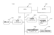
以下添付図面を参照して、本発明に係る半導体集積回路の配線設計装置及び半導体集積回路の配線設計用プログラムの実施形態を説明する。各図において同一の構成要素には、同一の符号を付して重複する説明を省略する。図2に実施形態に係る半導体集積回路の配線設計装置100のブロック図を示す。半導体集積回路の配線設計装置100は、サーバコンピュータ、パーソナルコンピュータ、その他のコンピュータにより構成することができる。
DESCRIPTION OF THE PREFERRED EMBODIMENTS Embodiments of a semiconductor integrated circuit wiring design apparatus and a semiconductor integrated circuit wiring design program according to the present invention will be described below with reference to the accompanying drawings. In each figure, the same components are denoted by the same reference numerals, and overlapping descriptions are omitted. FIG. 2 shows a block diagram of a
半導体集積回路の配線設計装置100は、CPU101が主メモリ102のプログラムやデータに基づき演算を行うものである。CPU101には、バス103及び外部記憶インタフェース304を介して外部記憶装置104が接続されており、外部記憶装置104には、半導体集積回路の配線設計用プログラムが記憶されている。CPU101が外部記憶装置104から半導体集積回路の配線設計用プログラムを主メモリ102へ読み出してこのプログラムを実行することにより半導体集積回路の配線設計装置100として機能する。
A
バス103には、外部記憶装置104以外に配線設計用情報供給部インタフェース305を介して半導体集積回路の配線設計用情報供給部105が接続されている。配線設計用情報供給部105は、外部の入力装置などから配線設計用情報を入力して保持するものとすることができ、或いは、外部の何らかの装置等で既に作成された配線設計用情報を取り込み保持したものとすることができる。更に、クライアントから提供された配線設計用情報を記憶した媒体がセットされることにより、配線設計用情報を保持し供給可能となっている装置であっても良い。更に、上記の構成を全て備えたものであっても良い。いずれにしても、CPU101が半導体集積回路の配線設計用プログラムを実行して配線設計用情報に基づき配線設計を行う場合には配線設計用情報はこの配線設計用情報供給部105から供給される。
The
配線設計用情報は、配線を行うために必要な情報であって、セルの位置情報及び大きさ情報、前記セル内のピンの位置情報及び大きさ情報、幹線配線の位置情報及び大きさ情報を含むものであリ、接続すべきピンの識別情報と幹線配線の識別情報のペアが含まれる。なお、大きさ情報は、セル、ピン、幹線配線のいずれのものについても、例えば四角の枠により規定されるものとし、四角形における対角線により結ばれる2つの角の座標によって表すものとすることができる。また、半導体集積回路自体については、設計済みであっても未設計であっても良く、上記配線設計用情報が作成されていれば良い。 The wiring design information is information necessary for wiring, and includes cell position information and size information, pin position information and size information in the cell, and main line position information and size information. It contains a pair of identification information of the pin to be connected and identification information of the main wiring. The size information for each of the cells, pins, and trunk lines is defined by, for example, a square frame, and can be represented by the coordinates of two corners connected by a diagonal line in the square. . Further, the semiconductor integrated circuit itself may or may not have been designed as long as the wiring design information is created.
バス103には、出力部インタフェース306を介して結果出力部106が接続されている。結果出力部106は、表示装置やプリンタなど、半導体集積回路の設計装置100において処理した結果を出力する装置とすることができる。また、結果出力部106は、半導体集積回路の配線設計装置100において処理した結果を記憶する媒体でもよく、更に、回線などを介して処理の依頼者(クライアント)へ処理結果を送信などする装置であっても良い。
A
本実施形態では、外部記憶装置104に記憶されている半導体集積回路の配線設計用プログラムが実行されることにより、図3に示される各手段が実現される。即ち、半導体集積回路の配線設計装置100は、図3に示されるように、始点支線発生手段201、最短距離接続手段202を具備している。
In this embodiment, each means shown in FIG. 3 is implemented by executing a wiring design program for a semiconductor integrated circuit stored in the
始点支線発生手段201は、セルの位置情報及び大きさ情報、上記セル内のピンの位置情報及び大きさ情報、幹線配線の位置情報及び大きさ情報を含む配線設計情報に基づき、複数の幹線配線中の所定数本の幹線配線を始点とし上記幹線配線に直交する幹線始点支線と、セル内のピンを始点とし上記幹線配線に直交するように延びるピン始点支線とを発生するものである。 The starting point branch line generating means 201 generates a plurality of trunk lines based on wiring design information including cell position information and size information, pin position information and size information in the cell, and trunk line position information and size information. A main line starting point branch line starting from a predetermined number of main lines in the cells and perpendicular to the main lines, and a pin starting point branch line starting from a pin in the cell and extending perpendicular to the main lines are generated.
最短距離接続手段202は、発生された上記幹線始点支線と発生された上記ピン始点支線とに関する発生支線情報及び上記配線設計情報に基づき、発生された上記幹線始点支線と発生された上記ピン始点支線が他の配線に重ならぬように最短距離で接続するものである。 The shortest distance connecting means 202 connects the generated main line start point branch line and the generated pin start point branch line based on the generated branch line information and the wiring design information regarding the generated trunk line start point branch line and the generated pin start point branch line. are connected at the shortest distance so that they do not overlap with other wiring.
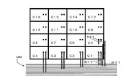
本実施形態では、半導体集積回路の配線設計装置100は、同じ大きさのセルであって、セル内の同じ位置にピンが配置されているセルが図4の如く縦横に複数並べられた半導体集積回路について配線設計を行う。図4は、4行4列でセルC1~C16が並べられたものである。各セルC1~C16の領域内に示されている2つのドットは、ピン位置を示している。
In this embodiment, the
本実施形態では、前記最短距離接続手段202は、上記幹線始点支線または上記ピン始点支線が他の配線と重なる場合には、上記幹線始点支線と上記ピン始点支線に直交する接続線を発生させて上記幹線始点支線と上記ピン始点支線とを接続する。また、最短距離接続手段202は、複数本の幹線配線に最も近接するセルのピンと幹線配線との間については、発生された上記幹線始点支線と発生された上記ピン始点支線とを直接接続した直線支線により接続を行う。
In this embodiment, the shortest
本実施形態では、前記始点支線発生手段201は、上記複数の幹線配線から数えて第1行目のセルにおけるピンと接続する幹線始点支線に隣接させて、複数の幹線配線から数えて第2行目のセルにおけるピンと接続する幹線始点支線を発生させる。また、上記複数の幹線配線から数えて第2行目のセルにおけるピンと接続する幹線始点支線に隣接させて、複数の幹線配線から数えて第3行目のセルにおけるピンと接続する幹線始点支線を発生させる。以下同様に、前行のセルにおけるピンと接続する幹線始点支線と次行のセルにおけるピンと接続する幹線始点支線とを隣接させて幹線始点支線を発生させる。 In this embodiment, the starting point branch line generating means 201 places the main line starting point branch line connected to the pin in the cell on the first row counted from the plurality of trunk wiring lines adjacent to the main line start branch line connected to the pin in the cell on the second row counted from the plurality of trunk wiring lines. Generate a trunk origin branch line that connects with a pin in a cell of . In addition, adjacent to the main line starting point branch line that connects to the pin in the cell on the second row counted from the plurality of trunk lines, a trunk line start point branch line that connects to the pin on the cell on the third line counted from the plurality of trunk lines is generated. Let In the same way, the main line starting point branch line connected to the pin in the previous row and the main line starting point branch line connecting to the pin in the next row cell are adjacent to each other to generate the main line starting point branch line.
以上の構成を有する第1の実施形態は、図5、図6に示されるフローチャートに対応するプログラムが実行されることにより実現される。本実施形態では、4列4行のセルであり、コラムiを1とし、ロウjを1とする(S11)。ピンを始点とするピン始点支線を発生し(S12)、このピン始点支線と直交する所要幹線配線の位置を始点として幹線始点支線を発生させる(S13)。ロウj=1であり、最も幹線配線に近い行のセルであるからピン始点支線と幹線始点支線を直線により接続して(コラムi,ロウj)=(1,1)の支線発生を完了する(S14)。 The first embodiment having the configuration described above is implemented by executing a program corresponding to the flowcharts shown in FIGS. In this embodiment, the cell is 4 columns and 4 rows, and the column i is set to 1 and the row j is set to 1 (S11). A pin starting point branch line is generated starting from the pin (S12), and a trunk starting point branch line is generated starting from the position of the required main line wiring orthogonal to the pin starting point branch line (S13). Since row j=1 and the cell is in the row closest to the main line, the pin starting point branch line and the main line starting point branch line are connected by a straight line to complete branch line generation for (column i, row j)=(1, 1). (S14).
次にコラムiを1歩進し(S15)、コラムi=5となっていないかを検出する(S16)。コラムi=5となっていない場合には、ステップS12へ戻って処理を続ける。ステップS16においてコラムi=5となっていることが検出された場合にはコラムi=1として(S17)、図6のフローチャートへ進み、ロウjを1歩進し(S21)、ロウj=5となっていないかを検出する(S22)。ロウj=5となっていない場合には、ピンを始点とするピン始点支線P21を発生し(S23)、他の配線と重なりがないかを検出する(S24)。この例では、重なりが生じるのでYESへ分岐し、上記複数の幹線配線MMから数えて第1行目のセルC1におけるピンと接続する幹線始点支線B11に隣接させて、複数の幹線配線MMから数えて第2行目のセルC5におけるピンと接続する幹線始点支線B21を発生させる(S25)。この様子を図7に示す。 Next, the column i is advanced by one (S15), and it is detected whether the column i=5 (S16). If column i is not equal to 5, the process returns to step S12 to continue processing. If column i=5 is detected in step S16, column i=1 is set (S17), the process proceeds to the flow chart of FIG. 6, row j is advanced by one (S21), and row j=5. (S22). If row j is not 5, a pin starting point branch line P21 is generated starting from the pin (S23), and it is detected whether or not there is an overlap with another wiring (S24). In this example, since there is an overlap, the branch is made to YES, counting from the plurality of main wirings MM, making it adjacent to the main wiring starting point branch line B11 connected to the pin in the cell C1 of the first row, counting from the plurality of main wirings MM. A main line starting point branch line B21 connected to the pin in cell C5 of the second row is generated (S25). This state is shown in FIG.
次に、上記は、幹線始点支線B21または上記ピン始点支線P21が他の配線と重なる場合に相当するので、上記幹線始点支線B21と上記ピン始点支線P21に直交する接続線J21を発生させて上記幹線始点支線B21と上記ピン始点支線P21とを接続する(S26)。この様子を図8に示す。 Next, since the above corresponds to the case where the main line start point branch line B21 or the pin start point branch line P21 overlaps with another wiring, a connection line J21 is generated that is orthogonal to the above-mentioned trunk line start point branch line B21 and the pin start point branch line P21, and the above The trunk starting point branch line B21 and the pin starting point branch line P21 are connected (S26). This state is shown in FIG.
ステップS26の次には、コラムiを1歩進し(S27)、コラムi=5となっていないかを検出する(S28)。コラムi=5となっていない場合には、ステップS23へ戻って処理を続ける。上記ステップS28においてコラムi=5となっていることが検出された場合には、コラムi=1として(S29)、次の行のセル内のピンからのピン始点支線の発生処理を行うためにステップS21へ戻る。このため、以下同様に、前行のセルにおけるピンと接続する幹線始点支線と次行のセルにおけるピンと接続する幹線始点支線とを隣接させて幹線始点支線を発生させる処理が行われる(S21~S29)。 After step S26, column i is advanced by one (S27), and it is detected whether column i=5 (S28). If column i is not equal to 5, the process returns to step S23 and continues. If column i=5 is detected in step S28, column i=1 is set (S29), and a pin starting point branch line is generated from the pin in the cell of the next row. Return to step S21. For this reason, in the same way, the main line starting point branch line connected to the pin in the previous row and the main line starting point branch line connecting to the pin in the next row cell are adjacent to each other to generate the main line starting point branch line (S21 to S29). .
本実施形態では、4行分の処理が行われたときに、ステップS22においてYESへ分岐することになり、処理は終了となる。このときに、図9に示すように全てのセルC1~C16のピンと複数の幹線配線MMの対応する幹線配線との間に、ピン始点支線(P××(××は、数字))で示した線)と幹線始点支線(B××で示した線)と接続線(J××で示した線)とにより構成される支線SSが設けられる。この支線SSは、前行のセルにおけるピンと接続する幹線始点支線と次行のセルにおけるピンと接続する幹線始点支線とを隣接させて幹線始点支線を発生させる処理を行っているために、接続線(J××で示した線)を最短にでき、最短距離の配線を実現している。 In this embodiment, when the processing for four lines has been performed, the process branches to YES in step S22, and the process ends. At this time, as shown in FIG. 9, pins of all the cells C1 to C16 and the corresponding trunk wires of the plurality of trunk wires MM are indicated by pin start branch lines (P×× (×× is a number)). A branch line SS is provided, which is composed of a main line starting point branch line (line indicated by Bxx) and a connecting line (line indicated by Jxx). Since this branch line SS is processed to generate a main line starting point branch line by adjoining the main line starting point branch line connecting to the pin in the previous row cell and the trunk line starting point branch line connecting to the pin in the next row cell, the connecting line ( The line indicated by Jxx) can be made the shortest, realizing wiring of the shortest distance.
次に第2の実施形態を説明する。この第2の実施形態では、上記第1の実施形態において発生させた接続線(J××で示した線)を用いない。本実施形態の始点支線発生手段201は、上記幹線始点支線または上記ピン始点支線が他の配線と重なる場合には、セルを横方向にシフトさせてシフトした位置のピンと複数の幹線配線との間で支線を発生させる。 Next, a second embodiment will be described. In this second embodiment, the connecting lines (lines indicated by Jxx) generated in the first embodiment are not used. When the main line starting point branch line or the pin starting point branch line overlaps with another wiring, the starting point branch line generating means 201 of this embodiment shifts the cell in the horizontal direction to generate a line between the pin at the shifted position and the plurality of main line lines. to generate a branch line.
シフトした位置のピンと複数の幹線配線との間で支線を発生させる場合において、ピンからは複数の幹線配線に直交する方向に延びるピン始点支線を発生させ、幹線配線の上記ピンに対応する位置から幹線配線に直交するようにピン方向へ延びる幹線始点支線を発生させる点は、第1の実施形態と同じである。発生させたピン始点支線と対応する幹線始点支線を直線的に接続する。 When branch lines are generated between a pin at a shifted position and a plurality of trunk lines, a pin starting point branch line extending in a direction orthogonal to the plurality of trunk lines is generated from the pin, and is generated from a position corresponding to the pin of the trunk line. It is the same as in the first embodiment in that a main line start point branch line extending in the pin direction is generated so as to be orthogonal to the main line wiring. The generated pin start point branch line and the corresponding trunk line start point branch line are connected linearly.
上記のようにすることから、図10に示すように上記複数の幹線配線MMに近いセルC1~C4のピンと上記複数の幹線配線MM中のセル側から遠い位置(図では下側)から幹線の選択を行って該当位置から幹線始点支線を発生する。即ち、幹線については配線トラックの順番<1>~<16>で選択し、セルのピンの選択は、「セルのピン選択順」の矢印に示される順で行う。この順は、セルの枠内に<1>~<16>で示されている。 From the above, as shown in FIG. 10, the pins of the cells C1 to C4 near the plurality of main lines MM and the positions far from the cell side in the plurality of main lines MM (lower side in the figure) are connected to the main lines. Select and generate a trunk line start point branch line from the corresponding position. That is, the main lines are selected in the order <1> to <16> of the wiring tracks, and the cell pins are selected in the order indicated by the arrows in the "cell pin selection order". This order is indicated by <1> to <16> in the frame of the cell.
発生された幹線始点支線と発生されたピン始点支線とを接続する順は、図11に示されるようになる。即ち、幹線については配線トラックの順番<1>~<16>で選択したものに対し、ピン始点支線としては図11の右側に描かれている矢印の通りに進む。つまり、ピン始点支線としてはセル枠内に[1]~[16]の順に幹線始点支線と接続してゆく。しかしながら、上記の通りにピン始点支線を発生させ、幹線始点支線を発生させた場合には、ピン始点支線は同じ列にあるから、そのままでは支線に重なりが生じる。 FIG. 11 shows the order in which the generated main line starting point branch line and the generated pin starting point branch line are connected. That is, the main line is selected in the order <1> to <16> of the wiring track, and the branch line at the pin start point proceeds as indicated by the arrows drawn on the right side of FIG. That is, as the pin starting point branch line, it connects to the main line starting point branch line in the order of [1] to [16] within the cell frame. However, when the pin start point branch line is generated and the main line start point branch line is generated as described above, the pin start point branch lines are in the same column, so the branch lines overlap.
始点支線発生手段201は、上記幹線始点支線または上記ピン始点支線が他の配線と重なる場合には、セルを横方向にシフトさせてシフトした位置のピンと複数の幹線配線との間で支線を発生させる。例えば、図12に示すように、第1行目のセルC1~C4については、当初の位置へ配置したままとし、第2行目のセルC5~C8については、セルC5~C8のピンから引き出したピン始点支線が第1行目のセルC1~C4のピンから引き出したピン始点支線と重ならないようにシフトを行う(ここでは、左シフト)。また、第3行目のセルC9~C12については、セルC9~C12のピンから引き出したピン始点支線が第2行目のセルC5~C8のピンから引き出したピン始点支線と重ならないようにシフトを行う(ここでは、左シフト)。更に、第4行目のセルC13~C16については、セルC13~C16のピンから引き出したピン始点支線が第3行目のセルC9~C12のピンから引き出したピン始点支線と重ならないようにシフトを行う(ここでは、左シフト)。 When the main line starting point branch line or the pin starting point branch line overlaps with another wiring, the starting point branch line generating means 201 shifts the cell in the horizontal direction to generate a branch line between the pin at the shifted position and the plurality of main line wirings. Let For example, as shown in FIG. 12, the cells C1 to C4 in the first row are left in their original positions, and the cells C5 to C8 in the second row are pulled out from the pins of the cells C5 to C8. A shift is performed so that the pin start point branch line obtained does not overlap with the pin start point branch line drawn from the pins of the cells C1 to C4 in the first row (here, left shift). In addition, the cells C9 to C12 in the third row are shifted so that the pin start branch lines drawn from the pins of the cells C9 to C12 do not overlap the pin start branch lines drawn from the pins of the cells C5 to C8 in the second row. (here, left shift). Further, the cells C13 to C16 in the fourth row are shifted so that the pin start branch lines drawn from the pins of the cells C13 to C16 do not overlap the pin start branch lines drawn from the pins of the cells C9 to C12 in the third row. (here, left shift).
また、始点支線発生手段201は、セルの大きさに応じてシフト量を決定してシフトを行う。例えば、セルの一部について示す図13のように、1行目のセルC01、C02、・・・が2行目以降のセルC5、・・・、C9、・・・、C13の大きさと異なる場合について説明する。この例では、4行目のセルはシフトせず、3行目から1行目のセルをシフトするものとする。すると、3行目から1行目のセルを同じ距離シフトした場合には、図13(A)に示すように、1行目のセルC01、C02が重なってしまう。係る場合には、1行目のセルC01、C02についてシフト量の調整を行い、図13(B)に示されるように1行目のセルC01、C02が重ならぬようにする。 Also, the starting point branch line generating means 201 determines the amount of shift according to the size of the cell and performs the shift. For example, as shown in FIG. 13 showing a part of cells, cells C01, C02, . A case will be described. In this example, it is assumed that the cells in the 4th row are not shifted and the cells in the 3rd to 1st rows are shifted. Then, when the cells in the third row to the first row are shifted by the same distance, the cells C01 and C02 in the first row overlap as shown in FIG. 13(A). In such a case, the shift amount is adjusted for the cells C01 and C02 in the first row so that the cells C01 and C02 in the first row do not overlap as shown in FIG. 13(B).
以上の構成を有する第2の実施形態は、図14に示されるフローチャートに対応するプログラムが実行されることにより実現される。本実施形態では、4列4行のセルである。まず、幹線配線の配線する順を入力する(S31)。ここでは、図10において説明したように、順番<1>~<16>と入力がなされる。次に既にセル配置の設計が完了しているか検出する(S32)。ステップS32においてNOへ分岐すると、セルが何行(ロウ)×何列(コラム)に配置されているかの情報を入力し(S34)、この情報に基づきセルの配置が行われる(S35)。一方、セル配置の設計が完了している場合には、設計済の情報(データ)からセルが何行(ロウ)×何列(コラム)に配置されているかの情報を取り出す(S33)。 The second embodiment having the above configuration is implemented by executing a program corresponding to the flowchart shown in FIG. In this embodiment, the cells are 4 columns and 4 rows. First, the order in which the trunk lines are wired is input (S31). Here, as described with reference to FIG. 10, the order <1> to <16> is input. Next, it is detected whether or not the cell placement design has already been completed (S32). When branched to NO in step S32, information on how many rows (rows) and how many columns (columns) the cells are arranged is input (S34), and the cells are arranged based on this information (S35). On the other hand, if the design of the cell layout has been completed, the information (row)×column (column) in which the cells are laid out is extracted from the designed information (data) (S33).
ステップS33またはステップS35に続いて、図10において説明した通り、幹線の配線トラックの順番を元に、可能な限り支線の長さが均等になるよう、「セルのピン選択順」を決定する(S36)。次に、図11において説明した通りに、セル配置の座標、ロウ位置、セルのセル枠サイズを基に支線の配線トラックの順番(配線順)を算出する(S37)。 Following step S33 or step S35, as described with reference to FIG. 10, the "cell pin selection order" is determined based on the order of wiring tracks of the main line so that the lengths of the branch lines are as uniform as possible ( S36). Next, as described with reference to FIG. 11, the order of wiring tracks (wiring order) of branch lines is calculated based on the coordinates of the cell arrangement, the row position, and the cell frame size of the cell (S37).
ステップS37に続いて図12において説明した通り、支線の配線トラックの順番、ピン図形の座標、配線ピッチの値を元にセル配置をシフトする(S38)。次に、シフトによりセルの重なりが生じないかを検出し(S39)、生じる場合には図13において説明した通りにシフト量を調整して適正な位置に配置する(S40)。以上によりセルの配置位置が確定となる(S41)。 After step S37, as described with reference to FIG. 12, the cell layout is shifted based on the wiring track order of the branch line, the coordinates of the pin figure, and the wiring pitch (S38). Next, it is detected whether or not the cells overlap due to the shift (S39), and if so, the amount of shift is adjusted as described with reference to FIG. Thus, the arrangement position of the cell is determined (S41).
上記でセルのシフトが完了したのかを検出し(S42)、NOとなるとステップS38へ戻って発生させるセルから延びる支線が他の配線(支線)と重ならないように処理を続ける。この結果、ステップS42においてYESへ分岐すると、ピン位置、幹線の配線トラックの順番の情報を基に、幹線を配線する(S43)。更に、幹線とセルのピンを支線で結線する(S44)。即ち、図12、図13により説明した通りのシフト後のセルのピンから発生させたピン始点支線と、幹線始点支線とを直線で結んで支線として配線を完了する。この結果、図15に示されるように、セルC1~C16からは幹線MMへ向けて直交するように延びた直線である支線SSによりピンと幹線MMの間が最短距離で接続される。 It is detected whether the shift of the cell is completed (S42), and if NO, the process returns to step S38 to continue the processing so that the branch line extending from the generated cell does not overlap other wiring (branch line). As a result, when branching to YES in step S42, the trunk line is wired based on the information of the pin position and the order of the wiring track of the trunk line (S43). Further, the main line and the pins of the cells are connected with branch lines (S44). That is, the pin start point branch line generated from the pin of the cell after shifting as explained with reference to FIGS. 12 and 13 and the main line start point branch line are connected by a straight line to complete the wiring as a branch line. As a result, as shown in FIG. 15, the pins and the main line MM are connected at the shortest distance by branch lines SS, which are straight lines extending perpendicularly from the cells C1 to C16 toward the main line MM.
また、図16に示す通り、ピンP1は幹線配線M1の端部で直線的に接続されれば良く、また、P1は幹線配線M1の端部で直線的に接続されれば良いので、無駄な配線を不要とでき、しかも最短距離で支線の配線を行うことができる。ピンP2と幹線配線M2、ピンP3と幹線配線M3、ピンP4と幹線配線M4についてもピンP1と幹線配線M1について述べた事項が成り立ち、図1に示した二重トラックを防ぐことができる。 Further, as shown in FIG. 16, the pin P1 may be connected linearly at the end of the main line M1, and the pin P1 may be connected linearly at the end of the main line M1. Wiring can be made unnecessary, and branch lines can be wired in the shortest distance. The pin P2 and the main wiring M2, the pin P3 and the main wiring M3, and the pin P4 and the main wiring M4 also hold the same as the pin P1 and the main wiring M1, so that the double tracks shown in FIG. 1 can be prevented.
なお、以上の実施形態では、1群の幹線配線MMの一方の側部に対してセル群が配置される半導体集積回路について述べてきたが、1群の幹線配線MMの両方の側部に対してセル群が配置される半導体集積回路について第1の実施形態と第2の実施形態は適用可能である。例えば、図17に示されるように1群の幹線配線MMに対し図の上側と図の下側にセル群が配置される場合を考える。 In the above embodiments, the semiconductor integrated circuit in which the cell group is arranged on one side of the group of main lines MM has been described. The first embodiment and the second embodiment can be applied to a semiconductor integrated circuit in which cell groups are arranged in the same direction. For example, as shown in FIG. 17, consider the case where cell groups are arranged on the upper side and the lower side of the drawing with respect to a group of trunk lines MM.
図17において、1群の幹線配線MMに対し図の上側に配置されているセル群のセルをC1U~C8Uとし、図の下側に配置されているセル群のセルをC1D~C8Dとする。係る場合に、図の上側の半導体集積回路についても図の下側の半導体集積回路についても、第1の実施形態の手法で動作する始点支線発生手段201と最短距離接続手段202とにより装置を構成することにより、第1の実施形態の例と同じように処理がなされ同様の効果を得ることができる。また、図の上側の半導体集積回路についても図の下側の半導体集積回路についても、第2の実施形態の実施形態の手法で動作する始点支線発生手段201と最短距離接続手段202とにより装置を構成することにより、第2の実施形態の例と同じように処理がなされ同様の効果を得ることができる。 In FIG. 17, the cells of the cell group arranged on the upper side of the figure with respect to one group of main wiring lines MM are C1U to C8U, and the cells of the cell group arranged on the lower side of the figure are assumed to be C1D to C8D. In such a case, both the semiconductor integrated circuit on the upper side of the figure and the semiconductor integrated circuit on the lower side of the figure are configured by the start point branch line generating means 201 and the shortest distance connecting means 202 that operate according to the method of the first embodiment. By doing so, the same processing as in the example of the first embodiment can be performed and the same effects can be obtained. In addition, for both the semiconductor integrated circuit on the upper side of the figure and the semiconductor integrated circuit on the lower side of the figure, the devices are connected by the start point branch line generating means 201 and the shortest distance connecting means 202 that operate according to the method of the second embodiment. With this configuration, processing can be performed in the same manner as in the example of the second embodiment, and similar effects can be obtained.
そして、図の上側の半導体集積回路のセル内のピン構成及び位置が、図の下側の半導体集積回路のセル内のピン構成及び位置と対象的である場合には、図の上側において設計される支線と図の上側において設計される支線とは、1群の幹線配線MMを挟んで対称となる。図17においては、図の上側のセルC5Uの1つのピンへ延びる支線S5Uと図の下側のセルC5Dの1つのピンへ延びる支線S5Dとは、1群の幹線配線MMを挟んで対称となる。このことから、図の上側の半導体集積回路のセル内のピンへ延びる全ての支線と対称的な下側の半導体集積回路のセル内のピンへ延びる全ての支線とは、1群の幹線配線MMを挟んで一直線となることから、支線の配線トラック(半導体集積回路における配線領域)として一連の位置に形成することができる。つまり、支線の配線トラックは共有ないしは一本化することができる。 If the pin configurations and positions within the cells of the semiconductor integrated circuit on the upper side of the diagram are symmetrical with the pin configurations and positions within the cells of the semiconductor integrated circuit on the lower side of the diagram, then the design on the upper side of the diagram is 1 and the branch line designed on the upper side of the figure are symmetrical with respect to the group of main wiring lines MM. In FIG. 17, the branch line S5U extending to one pin of the cell C5U on the upper side of the drawing and the branch line S5D extending to one pin of the cell C5D on the lower side of the drawing are symmetrical with respect to the group of main lines MM. . For this reason, all the branch lines extending to the pins in the cells of the semiconductor integrated circuit on the upper side of the figure and all the branch lines extending to the pins in the cells of the semiconductor integrated circuit on the lower side, which are symmetrical to each other, are a group of main wirings MM. , it can be formed in a series of positions as a branch line wiring track (wiring region in a semiconductor integrated circuit). That is, the wiring tracks of the branch lines can be shared or unified.
100 配線設計装置
102 主メモリ
103 バス
104 外部記憶装置
105 配線設計用情報供給部
106 結果出力部
201 始点支線発生手段
202 最短距離接続手段
304 外部記憶インタフェース
305 配線設計用情報供給部インタフェース
306 出力部インタフェース
REFERENCE SIGNS
Claims (12)
発生された前記幹線始点支線と発生された前記ピン始点支線とに関する発生支線情報及び前記配線設計情報に基づき、発生された前記幹線始点支線と発生された前記ピン始点支線が他の配線に重ならぬように最短距離で接続する最短距離接続手段と
を具備し、
前記最短距離接続手段は、複数本の幹線配線に最も近接するセルのピンと幹線配線との間については、発生された前記幹線始点支線と発生された前記ピン始点支線とを直接接続した直線支線により接続を行う
ことを特徴とする半導体集積回路の配線設計装置。 Based on wiring design information including cell position information and size information, pin position information and size information in the cell, and trunk line position information and size information, a predetermined number of trunk lines among a plurality of trunk lines. starting point branch line generating means for generating a main line starting point branch line starting from a wiring and perpendicular to the main wiring, and a pin starting branch line starting from a pin in a cell and extending perpendicular to the main wiring;
If the generated main line starting point branch line and the generated pin starting point branch line overlap another wiring based on the generated branch line information and the wiring design information regarding the generated main line starting point branch line and the generated pin starting point branch line. and a shortest distance connection means for connecting at the shortest distance without
The shortest-distance connecting means connects the pin of the cell closest to the plurality of main wires and the main wires by a straight branch line that directly connects the generated main-line starting point branch line and the generated pin-starting point branch line. make a connection
A wiring design device for a semiconductor integrated circuit, characterized by:
前記複数の幹線配線から数えて第1行目のセルにおけるピンと接続する幹線始点支線に隣接させて、複数の幹線配線から数えて第2行目のセルにおけるピンと接続する幹線始点支線を発生させ、
前記複数の幹線配線から数えて第2行目のセルにおけるピンと接続する幹線始点支線に隣接させて、複数の幹線配線から数えて第3行目のセルにおけるピンと接続する幹線始点支線を発生させ、
以下同様に、前行のセルにおけるピンと接続する幹線始点支線と次行のセルにおけるピンと接続する幹線始点支線とを隣接させて幹線始点支線を発生させることを特徴とする請求項3に記載の半導体集積回路の配線設計装置。 The start point branch line generating means is
generating a main line starting point branch line that is adjacent to the main line starting point branch line that connects to the pin in the cell on the first row counted from the plurality of main line lines and connects to the pin in the cell on the second line counted from the plurality of main line lines,
generating a main line starting point branch line that is adjacent to the main line starting point branch line that connects to the pin in the cell on the second row counted from the plurality of main line lines and connects to the pin in the cell on the third line counted from the plurality of main line lines,
4. The semiconductor device according to claim 3 , wherein the main line starting point branch line connected to the pin in the cell of the previous row and the main line starting point branch line connecting to the pin in the cell of the next row are similarly adjacent to each other to generate the trunk line starting point branch line. Wiring design equipment for integrated circuits.
セルの位置情報及び大きさ情報、前記セル内のピンの位置情報及び大きさ情報、幹線配線の位置情報及び大きさ情報を含む配線設計情報に基づき、複数の幹線配線中の所定数本の幹線配線を始点とし前記幹線配線に直交する幹線始点支線と、セル内のピンを始点とし前記幹線配線に直交するように延びるピン始点支線とを発生する始点支線発生手段、
発生された前記幹線始点支線と発生された前記ピン始点支線とに関する発生支線情報及
び前記配線設計情報に基づき、発生された前記幹線始点支線と発生された前記ピン始点支線が他の配線に重ならぬように最短距離で接続する最短距離接続手段
として機能させ、
前記コンピュータを前記最短距離接続手段として、
複数本の幹線配線に最も近接するセルのピンと幹線配線との間については、発生された前記幹線始点支線と発生された前記ピン始点支線とを直接接続した直線支線により接続を行うように機能させる
ことを特徴とする半導体集積回路の配線設計用プログラム。 the computer,
Based on wiring design information including cell position information and size information, pin position information and size information in the cell, and trunk line position information and size information, a predetermined number of trunk lines among a plurality of trunk lines. starting point branch line generating means for generating a main line starting point branch line starting from a wiring line and perpendicular to the main line line, and a pin starting point branch line starting from a pin in a cell and extending perpendicular to the main line line;
If the generated main line starting point branch line and the generated pin starting point branch line overlap another wiring based on the generated branch line information and the wiring design information regarding the generated main line starting point branch line and the generated pin starting point branch line. function as the shortest distance connection means to connect at the shortest distance without
With the computer as the shortest distance connection means,
Between the pin of the cell closest to the plurality of main wirings and the main wiring, a straight branch line that directly connects the generated main wiring start point branch line and the generated pin start point branch line functions to perform connection.
A wiring design program for a semiconductor integrated circuit, characterized by:
前記幹線始点支線または前記ピン始点支線が他の配線と重なる場合には、前記幹線始点支線と前記ピン始点支線に直交する接続線を発生させて前記幹線始点支線と前記ピン始点支線とを接続するように機能させることを特徴とする請求項7に記載の半導体集積回路の配線設計用プログラム。 With the computer as the shortest distance connection means,
When the main line start branch line or the pin start point branch line overlaps with another wiring, a connection line orthogonal to the trunk line start point branch line and the pin start point branch line is generated to connect the trunk line start point branch line and the pin start point branch line. 8. The wiring design program for a semiconductor integrated circuit according to claim 7 , wherein the program functions as described above.
前記複数の幹線配線から数えて第1行目のセルにおけるピンと接続する幹線始点支線に隣接させて、複数の幹線配線から数えて第2行目のセルにおけるピンと接続する幹線始点支線を発生させ、
前記複数の幹線配線から数えて第2行目のセルにおけるピンと接続する幹線始点支線に隣接させて、複数の幹線配線から数えて第3行目のセルにおけるピンと接続する幹線始点支線を発生させ、
以下同様に、前行のセルにおけるピンと接続する幹線始点支線と次行のセルにおけるピンと接続する幹線始点支線とを隣接させて幹線始点支線を発生させるように機能させることを特徴とする請求項9に記載の半導体集積回路の配線設計用プログラム。 With the computer as the starting point branch line generating means,
generating a main line starting point branch line that is adjacent to the main line starting point branch line that connects to the pin in the cell on the first row counted from the plurality of main line lines and connects to the pin in the cell on the second line counted from the plurality of main line lines,
generating a main line starting point branch line that is adjacent to the main line starting point branch line that connects to the pin in the cell on the second row counted from the plurality of main line lines and connects to the pin in the cell on the third line counted from the plurality of main line lines,
In the same way, the main line starting point branch line connected to the pin in the cell of the previous row and the main line starting point branch line connecting to the pin in the next row cell are made adjacent to each other to generate the trunk line starting point branch line. 3. A program for wiring design of a semiconductor integrated circuit according to .
前記幹線始点支線または前記ピン始点支線が他の配線と重なる場合には、セルを横方向にシフトさせてシフトした位置のピンと複数の幹線配線との間で支線を発生させるように機能させることを特徴とする請求項9または10に記載の半導体集積回路の配線設計用プログラム。 With the computer as the starting point branch line generating means,
When the main line starting point branch line or the pin starting point branch line overlaps with another wiring, the cell is shifted in the lateral direction so as to generate a branch line between the pin at the shifted position and the plurality of main wiring lines. 11. A wiring design program for a semiconductor integrated circuit according to claim 9 or 10 .
Priority Applications (1)
| Application Number | Priority Date | Filing Date | Title |
|---|---|---|---|
| JP2019125804A JP7139552B2 (en) | 2019-07-05 | 2019-07-05 | Semiconductor integrated circuit wiring design device and semiconductor integrated circuit wiring design program |
Applications Claiming Priority (1)
| Application Number | Priority Date | Filing Date | Title |
|---|---|---|---|
| JP2019125804A JP7139552B2 (en) | 2019-07-05 | 2019-07-05 | Semiconductor integrated circuit wiring design device and semiconductor integrated circuit wiring design program |
Publications (2)
| Publication Number | Publication Date |
|---|---|
| JP2021012935A JP2021012935A (en) | 2021-02-04 |
| JP7139552B2 true JP7139552B2 (en) | 2022-09-21 |
Family
ID=74227578
Family Applications (1)
| Application Number | Title | Priority Date | Filing Date |
|---|---|---|---|
| JP2019125804A Active JP7139552B2 (en) | 2019-07-05 | 2019-07-05 | Semiconductor integrated circuit wiring design device and semiconductor integrated circuit wiring design program |
Country Status (1)
| Country | Link |
|---|---|
| JP (1) | JP7139552B2 (en) |
Families Citing this family (1)
| Publication number | Priority date | Publication date | Assignee | Title |
|---|---|---|---|---|
| CN116956810B (en) * | 2023-08-01 | 2024-09-03 | 北京华大九天科技股份有限公司 | Wiring method and device, computing device and storage medium |
Citations (2)
| Publication number | Priority date | Publication date | Assignee | Title |
|---|---|---|---|---|
| JP2012084862A (en) | 2010-09-13 | 2012-04-26 | Semiconductor Energy Lab Co Ltd | Semiconductor device |
| US20170053054A1 (en) | 2015-08-20 | 2017-02-23 | Oracle International Corporation | Mitigating wire capacitance in an integrated circuit |
Family Cites Families (3)
| Publication number | Priority date | Publication date | Assignee | Title |
|---|---|---|---|---|
| JPH02278748A (en) * | 1989-04-19 | 1990-11-15 | Matsushita Electric Ind Co Ltd | Power supply wiring method |
| JPH02305472A (en) * | 1989-05-19 | 1990-12-19 | Fujitsu Ltd | Gate array with built-in cpu and manufacture thereof |
| JP2833453B2 (en) * | 1993-11-08 | 1998-12-09 | 日本電気株式会社 | Channel wiring method for semiconductor device |
-
2019
- 2019-07-05 JP JP2019125804A patent/JP7139552B2/en active Active
Patent Citations (2)
| Publication number | Priority date | Publication date | Assignee | Title |
|---|---|---|---|---|
| JP2012084862A (en) | 2010-09-13 | 2012-04-26 | Semiconductor Energy Lab Co Ltd | Semiconductor device |
| US20170053054A1 (en) | 2015-08-20 | 2017-02-23 | Oracle International Corporation | Mitigating wire capacitance in an integrated circuit |
Also Published As
| Publication number | Publication date |
|---|---|
| JP2021012935A (en) | 2021-02-04 |
Similar Documents
| Publication | Publication Date | Title |
|---|---|---|
| US10083269B2 (en) | Computer implemented system and method for generating a layout of a cell defining a circuit component | |
| JP4090118B2 (en) | LSI manufacturing method and recording medium recording layout program | |
| US7503026B2 (en) | Cell, standard cell, standard cell library, a placement method using standard cell, and a semiconductor integrated circuit | |
| JP3786398B2 (en) | Wiring method of semiconductor package | |
| US6245599B1 (en) | Circuit wiring system circuit wiring method semi-conductor package and semi-conductor package substrate | |
| JPH10313058A (en) | Semiconductor integrated circuit design apparatus, semiconductor integrated circuit design method, computer-readable recording medium storing semiconductor integrated circuit design program, and semiconductor integrated circuit manufacturing method | |
| JP4993362B2 (en) | Automatic delay adjustment method for semiconductor integrated circuit | |
| CN117764024A (en) | A clock tree comprehensive optimization method based on H-tree | |
| JP7139552B2 (en) | Semiconductor integrated circuit wiring design device and semiconductor integrated circuit wiring design program | |
| JP2006323643A (en) | Semiconductor integrated circuit floor plan design program, floor plan design apparatus, and design method | |
| JPH0421910B2 (en) | ||
| KR100216691B1 (en) | Layout input device and method and layout verification device and method | |
| JP2001306641A (en) | Automatic arranging and wiring method for semiconductor integrated circuit | |
| CN119067042A (en) | Chip layout generation method, device, computer equipment and storage medium | |
| Mattison | Design automation of MOS artwork | |
| JP5239766B2 (en) | Layout design method | |
| JPWO2013146276A1 (en) | Power system tree design support system and power system tree design method | |
| JP2921454B2 (en) | Wiring method of integrated circuit | |
| US6760896B2 (en) | Process layout of buffer modules in integrated circuits | |
| JP4907257B2 (en) | Circuit board wiring method and wiring support device | |
| US20030135837A1 (en) | Method and apparatus for automatic arrangement and wiring for a semiconductor integrated circuit design and wiring program therefor | |
| JP3141588B2 (en) | On-grid automatic wiring method | |
| JPH06216249A (en) | IC chip automatic layout design system | |
| JP2004157627A (en) | Placement and wiring program and semiconductor device manufacturing method | |
| JP2003282712A (en) | Wiring method for clock of semiconductor integrated circuit and semiconductor integrated circuit |
Legal Events
| Date | Code | Title | Description |
|---|---|---|---|
| A621 | Written request for application examination |
Free format text: JAPANESE INTERMEDIATE CODE: A621 Effective date: 20210719 |
|
| A977 | Report on retrieval |
Free format text: JAPANESE INTERMEDIATE CODE: A971007 Effective date: 20220510 |
|
| A131 | Notification of reasons for refusal |
Free format text: JAPANESE INTERMEDIATE CODE: A131 Effective date: 20220531 |
|
| A521 | Request for written amendment filed |
Free format text: JAPANESE INTERMEDIATE CODE: A523 Effective date: 20220726 |
|
| TRDD | Decision of grant or rejection written | ||
| A01 | Written decision to grant a patent or to grant a registration (utility model) |
Free format text: JAPANESE INTERMEDIATE CODE: A01 Effective date: 20220809 |
|
| A61 | First payment of annual fees (during grant procedure) |
Free format text: JAPANESE INTERMEDIATE CODE: A61 Effective date: 20220809 |
|
| R150 | Certificate of patent or registration of utility model |
Ref document number: 7139552 Country of ref document: JP Free format text: JAPANESE INTERMEDIATE CODE: R150 |
|
| R250 | Receipt of annual fees |
Free format text: JAPANESE INTERMEDIATE CODE: R250 |