JP7137913B2 - semiconductor equipment - Google Patents
semiconductor equipment Download PDFInfo
- Publication number
- JP7137913B2 JP7137913B2 JP2017123146A JP2017123146A JP7137913B2 JP 7137913 B2 JP7137913 B2 JP 7137913B2 JP 2017123146 A JP2017123146 A JP 2017123146A JP 2017123146 A JP2017123146 A JP 2017123146A JP 7137913 B2 JP7137913 B2 JP 7137913B2
- Authority
- JP
- Japan
- Prior art keywords
- layer
- oxide
- transistor
- conductive
- insulating layer
- Prior art date
- Legal status (The legal status is an assumption and is not a legal conclusion. Google has not performed a legal analysis and makes no representation as to the accuracy of the status listed.)
- Active
Links
Images


Description
本発明の一態様は、半導体装置に関する。本発明の一態様は、記憶装置に関する。 One embodiment of the present invention relates to a semiconductor device. One aspect of the present invention relates to a storage device.
なお、本発明の一態様は、上記の技術分野に限定されない。本明細書等で開示する本発明の一態様の技術分野としては、半導体装置、表示装置、発光装置、蓄電装置、記憶装置、電子機器、照明装置、入力装置、入出力装置、それらの駆動方法、又はそれらの製造方法、を一例として挙げることができる。 Note that one embodiment of the present invention is not limited to the above technical field. Technical fields of one embodiment of the present invention disclosed in this specification and the like include semiconductor devices, display devices, light-emitting devices, power storage devices, memory devices, electronic devices, lighting devices, input devices, input/output devices, and driving methods thereof. , or methods for producing them, can be mentioned as an example.
なお、本明細書等において、半導体装置とは、半導体特性を利用することで機能しうる装置全般を指す。トランジスタ、半導体回路、演算装置、記憶装置等は半導体装置の一態様である。また、撮像装置、電気光学装置、発電装置(薄膜太陽電池、有機薄膜太陽電池等を含む)、及び電子機器は半導体装置を有している場合がある。 Note that in this specification and the like, a semiconductor device refers to all devices that can function by utilizing semiconductor characteristics. A transistor, a semiconductor circuit, an arithmetic device, a memory device, or the like is one mode of a semiconductor device. Imaging devices, electro-optical devices, power generation devices (including thin-film solar cells, organic thin-film solar cells, etc.), and electronic devices may include semiconductor devices.
近年、扱われるデータ量の増大に伴って、より大きな記憶容量を有する半導体装置が求められている。単位面積あたりの記憶容量を増加させるためには、メモリセルを積層して形成することが有効である(特許文献1、特許文献2参照)。メモリセルを積層して設けることにより、単位面積当たりの記憶容量をメモリセルの積層数に応じて増加させることができる。
2. Description of the Related Art In recent years, as the amount of data to be handled increases, semiconductor devices with larger storage capacity are required. In order to increase the storage capacity per unit area, it is effective to stack memory cells (see
また、特許文献3には、酸化物半導体を用いた不揮発性の記憶装置が開示されている。
Further,
記憶装置はデータを格納するメモリセルアレイの他に、書き込みや読み出し動作を制御するための制御回路を有する。一般にメモリセルアレイの駆動電圧は制御回路よりも高いため、制御回路で生成された信号に基づいてメモリセルアレイを駆動する駆動回路には、高耐圧な素子が必要となる。しかしながら、このような高耐圧なトランジスタなどの素子は、制御回路を構成する素子よりもサイズが大きいため、メモリセルの数(すなわち記憶容量)が増大することに伴って、駆動回路を含む周辺回路の占有面積も増大してしまうといった問題があった。 A memory device has a memory cell array for storing data and a control circuit for controlling write and read operations. Since the drive voltage of the memory cell array is generally higher than that of the control circuit, the drive circuit that drives the memory cell array based on the signal generated by the control circuit requires elements with high withstand voltage. However, since such high-voltage transistors and other elements are larger in size than the elements that constitute the control circuit, the increase in the number of memory cells (that is, the storage capacity) leads to an increase in the number of peripheral circuits including the drive circuit. However, there is a problem that the occupied area is increased.
本発明の一態様は、周辺回路の占有面積を縮小することを課題の一とする。または、単位面積当たりの記憶容量の大きい半導体装置を提供することを課題の一とする。または、生産性の高い半導体装置を提供することを課題の一とする。または、新規な半導体装置、または記憶装置を提供することを課題の一とする。 An object of one embodiment of the present invention is to reduce the area occupied by a peripheral circuit. Another object is to provide a semiconductor device with a large memory capacity per unit area. Another object is to provide a highly productive semiconductor device. Another object is to provide a novel semiconductor device or memory device.
なお、これらの課題の記載は、他の課題の存在を妨げるものではない。なお、本発明の一態様は、これらの課題の全てを解決する必要はないものとする。なお、これら以外の課題は、明細書、図面、請求項などの記載から抽出することが可能である。 The description of these problems does not preclude the existence of other problems. Note that one embodiment of the present invention does not necessarily solve all of these problems. Problems other than these can be extracted from descriptions in the specification, drawings, claims, and the like.
本発明の一態様は、メモリトランジスタと、トランジスタと、を有する半導体装置である。メモリトランジスタは、第1の導電層、第2の導電層、第3の導電層、第1の絶縁層、第2の絶縁層、第3の絶縁層及び第1の半導体層を有する。トランジスタは、第4の導電層、第5の導電層、第4の絶縁層、及び第2の半導体層を有する。第1の導電層は開口を有し、第1の絶縁層は当該開口の内側に接して設けられ、第2の絶縁層は第1の絶縁層の内側に接して設けられ、第3の絶縁層は第2の絶縁層の内側に接して設けられ、第1の半導体層は第3の絶縁層の内側に接して設けられ、且つ、第1の導電層の開口よりも上下方向に突出して設けられる。また第2の導電層は第1の半導体層の底部に接して設けられ、第3の導電層は第1の半導体層の上部に接して設けられる。第4の導電層及び第5の導電層は、第2の半導体層にそれぞれ接して設けられる。第4の絶縁層は第2の半導体層に接して設けられる。第5の導電層は第4の絶縁層を介して第2の半導体層と重なる部分を有する。さらに、第1の絶縁層、第3の絶縁層、及び第4の絶縁層は、それぞれ酸化物を含む。さらに第2の絶縁層は、窒化物を含む。また、第1の半導体層と、第2の半導体層とは、同じ金属酸化物を含む。 One embodiment of the present invention is a semiconductor device including a memory transistor and a transistor. The memory transistor has a first conductive layer, a second conductive layer, a third conductive layer, a first insulating layer, a second insulating layer, a third insulating layer and a first semiconductor layer. The transistor has a fourth conductive layer, a fifth conductive layer, a fourth insulating layer, and a second semiconductor layer. The first conductive layer has an opening, the first insulating layer is provided in contact with the inner side of the opening, the second insulating layer is provided in contact with the inner side of the first insulating layer, and the third insulating layer is provided in contact with the inner side of the first insulating layer. The first semiconductor layer is provided in contact with the inner side of the second insulating layer, and the first semiconductor layer is provided in contact with the inner side of the third insulating layer and protrudes vertically beyond the opening of the first conductive layer. be provided. The second conductive layer is provided in contact with the bottom of the first semiconductor layer, and the third conductive layer is provided in contact with the top of the first semiconductor layer. A fourth conductive layer and a fifth conductive layer are provided in contact with the second semiconductor layer, respectively. A fourth insulating layer is provided in contact with the second semiconductor layer. The fifth conductive layer has a portion overlapping with the second semiconductor layer with the fourth insulating layer interposed therebetween. Additionally, the first insulating layer, the third insulating layer, and the fourth insulating layer each include an oxide. Furthermore, the second insulating layer includes nitride. Further, the first semiconductor layer and the second semiconductor layer contain the same metal oxide.
また、上記において、第3の導電層と、第4の導電層と、第5の導電層とは、互いに同じ金属元素を含むことが好ましい。 Further, in the above, the third conductive layer, the fourth conductive layer, and the fifth conductive layer preferably contain the same metal element.
また、上記において、第1の半導体層と、第2の半導体層とは、同じ金属酸化物膜を加工して形成されていることが好ましい。 Further, in the above, the first semiconductor layer and the second semiconductor layer are preferably formed by processing the same metal oxide film.
また、上記において、第3の導電層、第4の導電層、及び第5の導電層は、互いに同じ導電膜を加工して形成されていることが好ましい。 Further, in the above, the third conductive layer, the fourth conductive layer, and the fifth conductive layer are preferably formed by processing the same conductive film.
また、上記において、第1の導電層と、第4の導電層とは、電気的に接続されていることが好ましい。 Further, in the above, the first conductive layer and the fourth conductive layer are preferably electrically connected.
また、上記において、基板を有することが好ましい。このとき、メモリトランジスタは、当該基板上に複数設けられていることが好ましい。さらに、複数のメモリトランジスタは、基板の一面に対して垂直方向に積層して設けられていることが好ましい。 Moreover, in the above, it is preferable to have a substrate. At this time, it is preferable that a plurality of memory transistors be provided over the substrate. Furthermore, it is preferable that the plurality of memory transistors be stacked vertically with respect to one surface of the substrate.
また、上記において、第1の半導体層及び第2の半導体層は、第1の半導体膜と、第2の半導体膜の積層構造を有することが好ましい。このとき、第1の半導体膜と、第2の半導体膜とは、結晶性が異なることが好ましい。または、第1の半導体膜と、第2の半導体膜とは、組成が異なることが好ましい。 Further, in the above, the first semiconductor layer and the second semiconductor layer preferably have a stacked structure of the first semiconductor film and the second semiconductor film. At this time, it is preferable that the first semiconductor film and the second semiconductor film have different crystallinities. Alternatively, it is preferable that the first semiconductor film and the second semiconductor film have different compositions.
本発明の一態様によれば、周辺回路の占有面積を縮小できる。または、単位面積当たりの記憶容量の大きい半導体装置を提供できる。または、生産性の高い半導体装置を提供できる。または、新規な半導体装置、または記憶装置を提供できる。 According to one embodiment of the present invention, the area occupied by peripheral circuits can be reduced. Alternatively, a semiconductor device with a large memory capacity per unit area can be provided. Alternatively, a semiconductor device with high productivity can be provided. Alternatively, a novel semiconductor device or memory device can be provided.
なお、これらの効果の記載は、他の効果の存在を妨げるものではない。なお、本発明の一態様は、必ずしも、これらの効果の全てを有する必要はない。なお、これら以外の効果は、明細書、図面、請求項などの記載から抽出することが可能である。 Note that the description of these effects does not preclude the existence of other effects. Note that one embodiment of the present invention does not necessarily have all of these effects. Effects other than these can be extracted from descriptions in the specification, drawings, claims, and the like.
実施の形態について、図面を用いて詳細に説明する。但し、本発明は以下の説明に限定されず、本発明の趣旨及びその範囲から逸脱することなくその形態及び詳細を様々に変更し得ることは当業者であれば容易に理解される。従って、本発明は以下に示す実施の形態の記載内容に限定して解釈されるものではない。 Embodiments will be described in detail with reference to the drawings. However, the present invention is not limited to the following description, and those skilled in the art will easily understand that various changes can be made in form and detail without departing from the spirit and scope of the present invention. Therefore, the present invention should not be construed as being limited to the descriptions of the embodiments shown below.
なお、以下に説明する発明の構成において、同一部分又は同様な機能を有する部分には同一の符号を異なる図面間で共通して用い、その繰り返しの説明は省略する。また、同様の機能を指す場合には、ハッチパターンを同じくし、特に符号を付さない場合がある。 In the configuration of the invention to be described below, the same reference numerals are used in common for the same parts or parts having similar functions in different drawings, and repeated description thereof will be omitted. Moreover, when referring to similar functions, the hatch patterns may be the same and no particular reference numerals may be attached.
なお、本明細書で説明する各図において、各構成の大きさ、層の厚さ、または領域は、明瞭化のために誇張されている場合がある。よって、必ずしもそのスケールに限定されない。 In each drawing described in this specification, the size, layer thickness, or region of each configuration may be exaggerated for clarity. Therefore, it is not necessarily limited to that scale.
なお、本明細書等における「第1」、「第2」等の序数詞は、構成要素の混同を避けるために付すものであり、数的に限定するものではない。 Note that ordinal numbers such as “first” and “second” in this specification and the like are used to avoid confusion of constituent elements, and are not numerically limited.
トランジスタは半導体素子の一種であり、電流や電圧の増幅や、導通または非導通を制御するスイッチング動作などを実現することができる。本明細書におけるトランジスタは、IGFET(Insulated Gate Field Effect Transistor)や薄膜トランジスタ(TFT:Thin Film Transistor)を含む。 A transistor is a type of semiconductor element, and can achieve current or voltage amplification, switching operation for controlling conduction or non-conduction, and the like. A transistor in this specification includes an IGFET (Insulated Gate Field Effect Transistor) and a thin film transistor (TFT).
また、「ソース」や「ドレイン」の機能は、異なる極性のトランジスタを採用する場合や、回路動作において電流の方向が変化する場合などには入れ替わることがある。このため、本明細書においては、「ソース」や「ドレイン」の用語は、入れ替えて用いることができるものとする。 Also, the functions of "source" and "drain" may be interchanged when using transistors of different polarities or when the direction of current changes in circuit operation. Therefore, in this specification, the terms "source" and "drain" can be used interchangeably.
また、本明細書等において、トランジスタのソース、又はドレインのどちらか一方のことを「第1電極」と呼び、ソース、又はドレインの他方を「第2電極」とも呼ぶことがある。なお、ゲートについては「ゲート」又は「ゲート電極」とも呼ぶ。 In this specification and the like, either the source or the drain of a transistor may be called a "first electrode", and the other of the source and the drain may be called a "second electrode". Note that a gate is also called a “gate” or a “gate electrode”.
本明細書等において、金属酸化物(metal oxide)とは、広い表現での金属の酸化物である。金属酸化物は、酸化物絶縁体、酸化物導電体(透明酸化物導電体を含む)、酸化物半導体(Oxide Semiconductorまたは単にOSともいう)などに分類される。例えば、トランジスタの活性層に金属酸化物を用いた場合、当該金属酸化物を酸化物半導体と呼称する場合がある。つまり、OS FETと記載する場合においては、金属酸化物または酸化物半導体を有するトランジスタと換言することができる。 In this specification and the like, a metal oxide is a metal oxide in broad terms. Metal oxides are classified into oxide insulators, oxide conductors (including transparent oxide conductors), oxide semiconductors (also referred to as oxide semiconductors or simply OSs), and the like. For example, when a metal oxide is used for an active layer of a transistor, the metal oxide is sometimes called an oxide semiconductor. In other words, an OS FET can be referred to as a transistor including a metal oxide or an oxide semiconductor.
(実施の形態1)
本実施の形態では、本発明の一態様の半導体装置の構成例、作製方法例、回路構成、及びその動作方法例について説明する。
(Embodiment 1)
In this embodiment, a structure example, a manufacturing method example, a circuit structure, and an operation method example of a semiconductor device of one embodiment of the present invention will be described.
本発明の一態様は、メモリセルアレイと、高耐圧のトランジスタを含む回路部と、が同じ基板上に設けられた構成を有する。メモリセルアレイは、複数のメモリトランジスタが厚さ方向(縦方向)に積層された構成を有する。そのため、高耐圧のトランジスタをメモリセルアレイの近傍に配置することが可能となり、半導体装置の占有面積を縮小することができる。 One embodiment of the present invention has a structure in which a memory cell array and a circuit portion including high-voltage transistors are provided over the same substrate. The memory cell array has a structure in which a plurality of memory transistors are stacked in the thickness direction (vertical direction). Therefore, it is possible to arrange a high-voltage transistor in the vicinity of the memory cell array, so that the area occupied by the semiconductor device can be reduced.
ここで、メモリトランジスタが有する半導体層と、高耐圧のトランジスタが有する半導体層とは、同じ半導体膜を加工して形成される。これにより、各半導体層の形成工程を兼ねることができるため、作製工程を簡略化することができ、半導体装置の作製コストを低減できる。さらに、メモリセルアレイに接続される配線等と、高耐圧のトランジスタが有するソース電極、ドレイン電極、またはゲート電極等とが、同じ導電膜を加工して形成されることが好ましい。 Here, the semiconductor layer included in the memory transistor and the semiconductor layer included in the high-voltage transistor are formed by processing the same semiconductor film. As a result, the manufacturing process can be simplified and the manufacturing cost of the semiconductor device can be reduced because the process for forming each semiconductor layer can also be performed. Furthermore, it is preferable that the wirings and the like connected to the memory cell array and the source electrode, the drain electrode, the gate electrode, and the like of the high-voltage transistor are formed by processing the same conductive film.
また、メモリトランジスタと、高耐圧のトランジスタとがそれぞれ有する半導体層に、酸化物半導体を適用することが好ましい。酸化物半導体を用いたトランジスタは、シリコンを用いたトランジスタ等に比べて、ソース-ドレイン間の耐圧を高めることが可能なため、回路部を構成するトランジスタに好適に用いることができる。また酸化物半導体を用いたトランジスタは、シリコンに比べてゲート絶縁層の厚さを厚くしても駆動能力が低下しにくいという特徴を有するため、ゲート耐圧を向上させることが可能で、このようなトランジスタを回路部及びメモリトランジスタに用いることで、信頼性を高めることができる。 Further, an oxide semiconductor is preferably used for each of the semiconductor layers of the memory transistor and the high-voltage transistor. A transistor including an oxide semiconductor can have higher withstand voltage between a source and a drain than a transistor including silicon or the like, and thus can be suitably used as a transistor included in a circuit portion. In addition, since a transistor using an oxide semiconductor has a feature that driving capability is less likely to decrease even if the thickness of the gate insulating layer is increased compared to a transistor using silicon, it is possible to improve the gate breakdown voltage. Reliability can be improved by using a transistor for a circuit portion and a memory transistor.
ここで、メモリセルアレイを制御する制御回路上に重畳するように、上記メモリセルアレイや高耐圧トランジスタを含む回路部を設けることが好ましい。例えば制御回路を単結晶シリコン基板上に形成したCMOS回路等で構成し、その上部に、メモリセルアレイや回路部を形成することで実現できる。これにより、さらに半導体装置の占有面積を縮小することができるため、一枚の単結晶シリコン基板あたりのチップ数が増大し、作製コストを低減できる。 Here, it is preferable to provide a circuit portion including the memory cell array and the high-voltage transistor so as to overlap the control circuit for controlling the memory cell array. For example, it can be realized by configuring the control circuit with a CMOS circuit or the like formed on a single crystal silicon substrate, and forming a memory cell array and a circuit section thereon. Accordingly, the area occupied by the semiconductor device can be further reduced, so that the number of chips per single crystal silicon substrate can be increased and the manufacturing cost can be reduced.
以下では、より具体的な例について図面を参照して説明する。 A more specific example will be described below with reference to the drawings.
[構成例]
以下では、半導体装置700のメモリトランジスタ、メモリセルアレイ700M、及び回路部700Dが有するトランジスタの構成について、図面を参照して説明する。
[Configuration example]
The configurations of the memory transistors of the
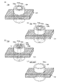
〔メモリセルアレイ〕
図1(A)は、半導体装置700の上面図であり、図1(B)は、図1(A)にA1-A2の一点鎖線で示す部位の断面図である。また、図1(C)は、図1(A)にA3-A4の一点鎖線で示す部位の断面図であり、メモリストリングを説明する断面図である。
[Memory cell array]
FIG. 1A is a top view of the
また、図1(D)は、図1(B)において、一点鎖線で囲まれた部分を拡大した断面図、または斜視図であり、メモリセルとして機能するメモリトランジスタを説明する図である。なお、以下においては、図1に示すように、x軸、y軸、z軸からなる直交座標系を便宜上設定して説明する。ここで、x軸およびy軸は、半導体装置700を設ける基板720の上面に平行にとり、z軸は基板720の上面に垂直にとる。
FIG. 1D is an enlarged cross-sectional view or perspective view of a portion surrounded by a dashed line in FIG. 1B, and is a diagram for explaining a memory transistor functioning as a memory cell. In the following, as shown in FIG. 1, an orthogonal coordinate system consisting of x-axis, y-axis, and z-axis is set for the sake of convenience. Here, the x-axis and y-axis are taken parallel to the top surface of the
半導体装置700は、基板720上に、メモリセルアレイ700Mと、回路部700Dとを有する。図1では、回路部700Dが有するトランジスタ750を示している。
A
メモリセルアレイ700Mは、基板720上に、複数の導電層701(導電層701_1乃至導電層701_m:mは、2以上の自然数)、導電層702、複数の絶縁層703(絶縁層703_1乃至絶縁層703_3)、複数の酸化物層704(酸化物層704_1乃至酸化物層704_3)、複数の導電層705(導電層705_1乃至導電層705_3)、複数の導電層706(導電層706_1乃至導電層706_3)、複数の接続層707(接続層707_1乃至接続層707_m)、複数の導電層708(導電層708_1乃至導電層708_m)、複数の絶縁層722、絶縁層724等を有する。
The
導電層701または導電層702と、絶縁層722とは交互に積層され、さらにこれを覆うように設けられた絶縁層724を含む積層体を構成する。絶縁層703は、該積層体を貫通するように形成された開口部の内側に設けられる。酸化物層704は、絶縁層703の内側に設けられる。導電層705は、酸化物層704の上端部と電気的に接続するように設けられる。導電層706は、酸化物層704の下端部と電気的に接続するように設けられる。接続層707は、導電層701と電気的に接続する。導電層708は、接続層707と電気的に接続する。
The
なお、図1(B)では、複数の導電層701を表すために、導電層701を3段以上表示しているが、本実施の形態は図1(B)に限られることなく、少なくとも導電層701を2段以上有していればよい。また図1(B)等では、x方向に配列する複数の柱状の開口部内に設けられる絶縁層703及び酸化物層704、並びに導電層706及び導電層705等を表すために、これらを3つ示しているが、これに限られることなく、少なくとも2つ以上有していればよい。
Note that three or more stages of the
ここで、図1(A)および図1(B)に示すように、導電層701はx軸方向に延伸して設けられる。また、図1(B)および図1(C)に示すように、絶縁層703および酸化物層704はz軸方向に延伸して設けられる。絶縁層703は、柱状の酸化物層704の側周辺を囲うように設けられている。つまり、導電層701と、絶縁層703および酸化物層704と、は互いに垂直に交差して設けられることが好ましい。また、図1(B)に示すように、接続層707は柱状に形成されており、z軸方向に延伸して設けられる。また、導電層708をy軸方向に延伸して設けてもよい。また、導電層705に接続される配線BLとして機能する導電層をy軸方向に延伸して設けてもよい。なお、導電層705の一部を配線BLとして機能させ、当該導電層をy軸方向に延伸して設けてもよい。
Here, as shown in FIGS. 1A and 1B, the
柱状の酸化物層704は、z軸方向の下端において、導電層706と電気的に接続し、上端において、導電層705と電気的に接続する。また、図1(C)に示すように、導電層706は、隣り合う2つの柱状の酸化物層704の下端と電気に接続し、該2つの柱状の酸化物層704の上端は、それぞれ、電気的に分離した導電層705と、電気的に接続する。
The
ここで、導電層701と、絶縁層703および酸化物層704と、が交差する領域近傍がメモリトランジスタ(メモリトランジスタ710)として機能する。また、導電層702と、絶縁層703および酸化物層704と、が交差する領域近傍が選択トランジスタ(ビット線側選択トランジスタ:SDT、またはソース線側選択トランジスタ:SST)として機能する。これらのメモリトランジスタおよび選択トランジスタのチャネル長方向はz軸に平行になる。メモリトランジスタまたは選択トランジスタが電気的に直列に接続されており、これらがメモリストリングを構成している。
Here, the vicinity of a region where the
なお、本実施の形態に示す半導体装置の構成は一例であり、本発明は、本実施の形態に係る図面等に示す、回路素子および配線等の、個数および配置等に限定されるものではない。本実施の形態に係る半導体装置が有する、回路素子および配線等の、個数および配置等は、回路構成や駆動方法に合わせて適宜設定することができる。 Note that the configuration of the semiconductor device shown in this embodiment is an example, and the present invention is not limited to the number, arrangement, etc. of circuit elements, wiring, etc. shown in the drawings and the like according to this embodiment. . The number, arrangement, and the like of circuit elements, wirings, and the like included in the semiconductor device according to this embodiment can be appropriately set according to the circuit configuration and the driving method.
メモリセルアレイ700M及び回路部700Dを設ける基板720は絶縁表面を有していることが好ましい。絶縁表面を有する基板としては、表面に絶縁膜が形成された半導体基板、絶縁性基板、表面に絶縁膜が形成された導電性基板などを用いればよい。半導体基板としては、例えば、シリコン、ゲルマニウムなどの単体半導体基板、または炭化シリコン、シリコンゲルマニウム、ヒ化ガリウム、リン化インジウム、酸化亜鉛、酸化ガリウムなどの半導体基板などを用いればよい。また、絶縁性基板としては、例えば、ガラス基板、石英基板、サファイア基板、安定化ジルコニア基板(イットリア安定化ジルコニア基板など)、樹脂基板などを用いればよい。また、前述の半導体基板内部に絶縁性の領域を有する半導体基板、例えばSOI(Silicon On Insulator)基板などを用いてもよい。また、導電性基板としては、黒鉛基板、金属基板、合金基板、導電性樹脂基板などを用いればよい。
The
導電層701は、メモリトランジスタ710のゲートとして機能し、ワード線と電気的に接続する。すなわち、導電層701、接続層707、および導電層708は、ワード線の一部としても機能する。ここで、導電層701は、図1(B)に示すように、下層の導電層701が上層の導電層701よりA2側に延伸した、階段状に設けられることが好ましい。このように、導電層701を設けることにより、下層の導電層701の上面の一部の領域が、より上層の導電層701と重ならないため、導電層701各層の当該領域と各接続層707を接続させることができる。
導電層701として、シリコンや、金属など、導電性を有する材料を用いることができる。導電層701として、シリコンを用いる場合、アモルファスシリコンや、ポリシリコンを用いることができる。また、シリコンに導電性を持たせるため、p型不純物やn型不純物を添加してもよい。また、シリコンを含む導電性材料として、チタン、コバルト、またはニッケルを含むシリサイドを導電層701として用いることができる。また、金属材料を導電層701に用いる場合、アルミニウム、クロム、銅、銀、金、白金、タンタル、ニッケル、チタン、モリブデン、タングステン、ハフニウム、バナジウム、ニオブ、マンガン、マグネシウム、ジルコニウム、ベリリウム、インジウム、ルテニウムなどから選ばれた金属元素を1種以上含む材料を用いることができる。
As the
導電層702は、絶縁層722を介して導電層701の上に設けられる。導電層702は、選択トランジスタ(ビット線側選択トランジスタ:SDT、およびソース線側選択トランジスタ:SST)のゲートとして機能する。また、導電層702は、導電層701と同様の材料を用いることができる。また、導電層702は、導電層701と同じ材料を用いてもよいし、異なる材料を用いてもよい。導電層701、および導電層702は、用途に応じて、仕事関数などを考慮し、決定すればよい。
The
導電層701および導電層702の、上層または下層に設けられる絶縁層722として、絶縁性を有する酸化物、窒化物、酸化窒化物、窒化酸化物、金属酸化物、金属酸化窒化物、金属窒化酸化物などを用いることができる。酸化シリコン、酸化窒化シリコン、窒化酸化シリコン、窒化シリコン、フッ素を添加した酸化シリコン、炭素を添加した酸化シリコン、炭素および窒素を添加した酸化シリコン、もしくは空孔を有する酸化シリコンまたは樹脂は、比誘電率が低いため、絶縁層722に用いることは好適である。
As the insulating
一方、絶縁層722として、酸化アルミニウム、酸化ガリウム、酸化ハフニウム、酸化ジルコニウム、アルミニウムおよびハフニウムを有する酸化物、アルミニウムおよびハフニウムを有する酸化窒化物、シリコンおよびハフニウムを有する酸化物、シリコンおよびハフニウムを有する酸化窒化物またはシリコンおよびハフニウムを有する窒化物などを用いることも可能だが、これらは比誘電率が高いため、2つの導電層701の間、または導電層701と導電層702との間に寄生容量が生じる場合がある。そのため、デバイスの設計、用途に応じて絶縁層722に用いる材料を決めることができる。
On the other hand, as the insulating
また、導電層701、導電層702等を覆う絶縁層724としては、絶縁層722と同様の材料を用いることができる。
For the insulating
酸化物層704、絶縁層703、および導電層701(導電層701_1乃至導電層701_mのいずれか一)により、メモリトランジスタ710が構成される。図1(B)、(C)には、メモリトランジスタ710がm段(mは2以上の自然数)積層している例を示している。
A
導電層705は、酸化物層704と電気的に接続し、ソース線SL、またはビット線BLの一部として機能する。導電層705として、金属元素を含む導電性材料を用いることが好ましい。また、導電層705と酸化物層704の界面には、導電層705が有する金属元素と、酸化物層704の成分とを含む金属化合物層が形成されていることが好ましい。該金属化合物が形成されることで、導電層705と、酸化物層704とのコンタクト抵抗が低減するため好ましい。または、酸化物層704に含まれる酸素を、導電層705が吸収し、酸化物層704の、導電層705と酸化物層704の界面近傍の抵抗を低減することで、導電層705と、酸化物層704とのコンタクト抵抗を低減することができる。
導電層705として、アルミニウム、ルテニウム、チタン、タンタル、クロム、タングステン、および銅から選ばれた一、または複数の金属元素を含む導電性材料を用いることが好ましい。
A conductive material containing one or more metal elements selected from aluminum, ruthenium, titanium, tantalum, chromium, tungsten, and copper is preferably used for the
導電層706は、図1(C)に示すように、ビット線BLの一部として機能する導電層705と電気的に接続する酸化物層704と、ソース線SLの一部として機能する導電層705と電気的に接続する酸化物層704と、電気的に接続することで、メモリストリングを構成する。図1(A)中の一点鎖線で囲まれた領域は、1つのメモリストリングを表している。なお、図1(A)では3つのメモリストリングが明示されているが、実際には1つのメモリセルアレイが有するメモリストリングの数は偶数であることが好ましく、2n(nは1以上の自然数)であることがより好ましい。
As shown in FIG. 1C, the
導電層706は、導電層705と同様の材料を用いることができる。また、導電層706は、導電層705と同じ材料を用いてもよいし、異なる材料を用いてもよい。
A material similar to that of the
また、導電層706と酸化物層704の界面には、導電層706が有する金属元素と、酸化物層704の成分とを含む金属化合物層が形成されていることが好ましい。該金属化合物が形成されることで、導電層706と、酸化物層704とのコンタクト抵抗が低減するため好ましい。または、酸化物層704に含まれる酸素を、導電層706が吸収し、酸化物層704の、導電層706と酸化物層704の界面近傍の抵抗を低減することで、導電層706と、酸化物層704とのコンタクト抵抗を低減することができる。
A metal compound layer containing a metal element included in the
図1(D)は、1つのメモリトランジスタ710及びその近傍の拡大図を示している。図1(D)に示すように、絶縁層703は、絶縁層703a、絶縁層703b、および絶縁層703cを有する。絶縁層703aは、導電層701側に設けられ、絶縁層703cは、酸化物層704側に設けられ、絶縁層703bは、絶縁層703aと絶縁層703cの間に設けられる。絶縁層703aはゲート絶縁層として機能し、絶縁層703bは電荷蓄積層として機能し、絶縁層703cはトンネル絶縁層として機能する。
FIG. 1D shows an enlarged view of one
ここで、図2(A)には、1つのメモリトランジスタ710及びその近傍の斜視図を示している。
Here, FIG. 2A shows a perspective view of one
絶縁層703aとして、酸化シリコンや、酸化窒化シリコンを用いることが好ましい。また、酸化アルミニウム、酸化ハフニウム、またはアルミニウムおよびハフニウムを有する酸化物を用いてもよい。また、これらを積層して絶縁層703aとしてもよい。
Silicon oxide or silicon oxynitride is preferably used for the insulating
絶縁層703bは、電荷蓄積層として機能する材料を用いることが好ましく、窒化シリコンや、窒化酸化シリコンを用いることが好ましい。また、酸化アルミニウム、酸化ハフニウム、またはアルミニウムおよびハフニウムを有する酸化物を用いてもよい。
The insulating
絶縁層703cとして、酸化シリコンや、酸化窒化シリコンを用いることが好ましい。また、酸化アルミニウム、酸化ハフニウム、またはアルミニウムおよびハフニウムを有する酸化物を用いてもよい。また、これらを積層して絶縁層703cとしてもよい。また、絶縁層703cは、絶縁層703aより薄いことが好ましい。詳細は後述するが、メモリトランジスタへのデータの書き込み、または消去において、絶縁層703cを通って、酸化物層704と絶縁層702bの間で、電荷の移動が行われる。すなわち、絶縁層703cは、トンネル絶縁層として機能する。
Silicon oxide or silicon oxynitride is preferably used for the insulating
特に、導電層701、導電層702、および絶縁膜を有する積層体に設けられた開口に絶縁層703を形成する場合、開口の底部に形成された絶縁層703は、ドライエッチングなどを用いた異方性エッチングにより除去する必要がある。異方性エッチングの際、絶縁層703cは、側面においても、プラズマ、ラジカル、ガス、薬液などに曝される。これらによって絶縁層703cの側面がダメージを受けると、絶縁層703cにトラップセンターが生じ、トランジスタの電気特性に影響を与える場合がある。トラップセンターの生成を抑制するためには、絶縁層703cの側面は、エッチングによるダメージに対して高い耐性を有していることが求められる。この場合、絶縁層703cとして、酸化アルミニウム、酸化シリコンと酸化アルミニウムの積層、または酸化窒化シリコンと酸化アルミニウムの積層を用いることが好ましい。
In particular, when the insulating
絶縁層703a、絶縁層703b、および絶縁層703cは、ALD法やCVD法を用いて形成することができる。また、絶縁層703a、絶縁層703b、および絶縁層703cの界面の汚染を防ぐためには、同一チャンバー内で、または複数のチャンバーを有するマルチチャンバ方式の成膜装置を用いて、大気雰囲気に曝すことなく、連続で成膜することが好ましい。
The insulating
酸化物層704は、酸化物半導体として機能する金属酸化物(以下、酸化物半導体ともいう)を用いることが好ましい。酸化物半導体は、シリコンなどからなる半導体と比較して、トランジスタのオン特性が良好で、高い移動度が得られるため、好ましい。
A metal oxide that functions as an oxide semiconductor (hereinafter also referred to as an oxide semiconductor) is preferably used for the
例えば、酸化物層704として、In-M-Zn酸化物(元素Mは、アルミニウム、ガリウム、イットリウム、銅、バナジウム、ベリリウム、ホウ素、チタン、鉄、ニッケル、ゲルマニウム、ジルコニウム、モリブデン、ランタン、セリウム、ネオジム、ハフニウム、タンタル、タングステン、またはマグネシウムなどから選ばれた一種、または複数種)等の金属酸化物を用いるとよい。また、酸化物層704として、In-Ga酸化物、In-Zn酸化物を用いてもよい。
For example, as the
図2(B)、(C)には、酸化物層704を積層構造とした場合の例を示している。
2B and 2C show an example in which the
図2(B)に示すように、メモリトランジスタ710は絶縁層703c側に設けられる酸化物層704aと酸化物層704aの内側に設けられる酸化物層704bを有することが好ましい。このとき、酸化物層704aは、酸化物層704bに対して、相対的にエネルギーギャップの広い酸化物を用いることが好ましい。ここで、エネルギーギャップの広い酸化物を、ワイドギャップ、エネルギーギャップの狭い酸化物をナローギャップと呼ぶことがある。
As shown in FIG. 2B, the
酸化物層704aをナローギャップとし、酸化物層704bをワイドギャップとする場合、酸化物層704aの伝導帯下端のエネルギーが、酸化物層704bの伝導帯下端のエネルギーより高くなることが好ましい。また、言い換えると、酸化物層704aの電子親和力が、酸化物層704bの電子親和力より小さいことが好ましい。
When the
また、酸化物層704aと酸化物層704bは、各金属原子の原子数比が異なる組み合わせにすることが好ましい。具体的には、酸化物層704aに用いる金属酸化物において、構成元素中の元素Mの原子数比が、酸化物層704bに用いる金属酸化物における、構成元素中の元素Mの原子数比より、大きいことが好ましい。また、酸化物層704aに用いる金属酸化物において、Inに対する元素Mの原子数比が、酸化物層704bに用いる金属酸化物における、Inに対する元素Mの原子数比より大きいことが好ましい。また、酸化物層704bに用いる金属酸化物において、元素Mに対するInの原子数比が、酸化物層704aに用いる金属酸化物における、元素Mに対するInの原子数比より大きいことが好ましい。
In addition, it is preferable that the
酸化物層704aには、例えばIn:Ga:Zn=1:3:4、In:Ga:Zn=1:3:2、またはIn:Ga:Zn=1:1:1の組成およびその近傍の組成を有する金属酸化物を用いることができる。また、酸化物層704bには、例えばIn:Ga:Zn=4:2:3から4.1、In:Ga:Zn=1:1:1、またはIn:Ga:Zn=5:1:6の組成およびその近傍の組成を有する金属酸化物を用いることができる。これらの酸化物層704aおよび酸化物層704bを上記の原子数比の関係を満たして組み合わせることが好ましい。例えば、酸化物層704aを、In:Ga:Zn=1:3:4の組成およびその近傍の組成を有する金属酸化物、酸化物層704bを、In:Ga:Zn=4:2:3から4.1の組成およびその近傍の組成を有する金属酸化物とするのが好ましい。なお、上記組成は、基板上に形成された酸化物中の原子数比、またはスパッタターゲットにおける原子数比を示す。
The
また、酸化物層704aとして、後述する、CAAC-OSを用い、酸化物層704bとして、CAC-OSを用いることが好ましい。酸化物層704aとして、CAAC-OSを用いる場合、c軸は、図1(A)などに示すx-y平面に平行、すなわちz軸に垂直で、かつ開口の側面から中心に向かうように配向することが好ましい。
Further, CAAC-OS, which will be described later, is preferably used for the
ここで、酸化物層704aと酸化物層704bの接合部において、伝導帯下端はなだらかに変化する。換言すると、酸化物層704aと酸化物層704bの接合部における伝導帯下端は、連続的に変化または連続接合するともいうことができる。このようにするためには、酸化物層704aと酸化物層704bとの界面において形成される混合層の欠陥準位密度を低くするとよい。
Here, the bottom of the conduction band changes smoothly at the junction between the
具体的には、酸化物層704aと酸化物層704bが、酸素以外に共通の元素を有する(主成分とする。)ことで、欠陥準位密度が低い混合層を形成することができる。例えば、酸化物層704bがIn-Ga-Zn酸化物の場合、酸化物層704aとして、In-Ga-Zn酸化物、Ga-Zn酸化物、酸化ガリウムなどを用いるとよい。これにより、酸化物層704aと酸化物層704bとの界面における欠陥準位密度を低くすることができる。そのため、界面散乱によるキャリア伝導への影響が小さくなり、メモリトランジスタ710は高いオン電流を得られる。
Specifically, when the
図2(B)に示すように、酸化物層704bは、酸化物層704aに囲まれるように設けられている。このような構成の場合、酸化物層704に、導電層705から導電層706への方向、あるいは導電層706から導電層705への方向(すなわちz軸方向)にキャリアを流す際、ナローギャップを有する成分において、主にキャリアが流れる。このため、上記構成を用いる場合、トランジスタのオン状態において高い電流駆動力、つまり大きなオン電流、及び高い電界効果移動度を得ることができる。
As shown in FIG. 2B, the
また、酸化物層704bと、絶縁層703cと、の間に酸化物層704aを設けることで、キャリアパスとなる酸化物層704bと、絶縁層703cが直接接することがなく、トラップセンターの形成を抑制することができる。半導体(酸化物半導体)と、絶縁層との界面に形成されたトラップセンターは、電子を捕獲し、トランジスタのしきい値電圧をプラス方向に変動させるため、トランジスタの信頼性や、オン、オフ特性に悪影響を及ぼす恐れがある。よって、当該酸化物を用いるトランジスタは、トラップセンターによる電気特性の影響を受けることがないため、オン状態においてより高い電流駆動力、つまり大きなオン電流、及び高い電界効果移動度を得ることができる。また、当該トランジスタ、および当該トランジスタを用いた半導体装置は、高い信頼性を得ることができる。
In addition, by providing the
図2(D)に示すメモリトランジスタ710は、絶縁層703a、絶縁層703b、および絶縁層703cの内側に、酸化物層704aが設けられ、酸化物層704aの内側に酸化物層704bが設けられ、酸化物層704bの内側に酸化物層704cが設けられている。また、酸化物層704cの内側には、絶縁層711が埋め込まれるように設けられていてもよい。なお、絶縁層711は、必ずしも設けなくてよく、酸化物層704cの内側は、空洞でもよい。
In the
酸化物層704bは、酸化物層704a、および酸化物層704cに挟まれるように設けられる。このとき、酸化物層704cは、酸化物層704aと同様にワイドギャップであることが好ましい。ワイドギャップである酸化物層704cを設けることで、酸化物層704を流れるキャリアを酸化物層704bに閉じ込めることができ、トランジスタのオン状態において高い電流駆動力、つまり大きなオン電流、及び高い電界効果移動度を得ることができる。
The
また、酸化物層704cの内側に絶縁層711を設ける場合、絶縁層711は、酸化物層704に酸素を供給できる材料であることが好ましい。絶縁層711として、水素や窒素を極力含まない酸化物を用いることで、酸化物層704に酸素を供給できる場合がある。酸化物層704に酸素を供給することで、酸化物層704中に含まれる水素や水などの不純物を除去することができ、酸化物層704は高純度化する。不純物が極力低減された酸化物を酸化物層704として用いることで、メモリトランジスタ、および当該トランジスタを用いた半導体装置は、高い信頼性を得ることができる。
In the case where the insulating
また、絶縁層711として、水素や窒素などの不純物を供給できる材料を用いることもできる。絶縁層711に水素や窒素を含む酸化物を用いることで、酸化物層704に水素や窒素を供給できる場合がある。酸化物層704に水素や窒素を供給することで、酸化物層704の抵抗値が下がる場合がある。酸化物層704の抵抗値を、回路動作の弊害にならない程度に下げることで、より低い駆動電圧で、メモリトランジスタを動作させることができる。また、メモリトランジスタのオン状態において高い電流駆動力、つまり大きなオン電流、及び高い電界効果移動度を得ることができる。
Alternatively, a material capable of supplying impurities such as hydrogen or nitrogen can be used for the insulating
図2(D)には、選択トランジスタ(ビット線側トランジスタ:SDT、またはソース線側トランジスタ:SST)及びその近傍における斜視図を示している。 FIG. 2D shows a perspective view of a selection transistor (bit line side transistor: SDT or source line side transistor: SST) and its vicinity.
図2(D)に示すように、選択トランジスタには電荷蓄積層を設けなくてもよい。よって、ビット線側トランジスタ:SDT、およびソース線側トランジスタ:SSTにおいて、絶縁層703として絶縁層703bおよび絶縁層703cを設けず、絶縁層703aのみを設ける構成にしてもよい。
As shown in FIG. 2D, the selection transistor need not be provided with a charge storage layer. Therefore, in the bit line side transistor: SDT and the source line side transistor: SST, only the insulating
なお、図2(D)において、酸化物層704を単層で示しているが、これに限らない。酸化物層704は、上記で例示した、2層構造または3層構造としてもよいし、4層以上の積層構造でもよい。また、酸化物層704の内側に、絶縁層711が設けられていてもよい。
Note that although the
なお、メモリトランジスタ710が設けられる、積層体に形成された開口は、図1(A)や、図2の各図において、上面を円形状としているがこれに限られるものではなく、例えば上面を楕円形状としてもよいし、三角形、四角形などの多角形状にしてもよい。また、多角形状とする場合、角部が丸みを帯びている形状としてもよい。また、当該開口の上面形状や断面形状に合わせて、絶縁層703、および酸化物層704の上面形状や断面形状も変化することがある。また、当該開口は、上方(導電層705側)の開口の断面積と比較して、下方(導電層706側)の開口の断面積が狭くなるような形状としてもよい。
Note that the opening formed in the stacked body in which the
〔接続構成例〕
図3は、メモリトランジスタを6段有するメモリセルアレイ700Mを複数組み合わせた記憶装置700Aを説明する上面図である。なお、図3では、説明を容易にするため、一部の構成要素を省略している。例えば、導電層701上に設けられる選択トランジスタ(ビット線側トランジスタ:SDT、およびソース線側トランジスタ:SST)や、それらの構成要件である導電層702は、省略している。また、ビット線BLやソース線SLの一部として機能する導電層705、およびワード線WLの一部として機能する導電層708は、実線にて示している。
[Connection configuration example]
FIG. 3 is a top view for explaining a
記憶装置700Aにおいて、各メモリセルアレイ700Mは、6段のメモリトランジスタを有するメモリストリングを4つ有する。
In the
メモリストリングのビット線側の端は、それぞれ異なるビット線BL(BL_1乃至BL_4)と電気的に接続する。一方、メモリストリングのソース線側の端は、ソース線SLと電気的に接続されており、共通の電位が与えられている。ソース線SLは、接地されていてもよいし、一定の電位が与えられていてもよい。また、回路の動作に合わせて、電位を変動させてもよい。 The ends of the memory strings on the bit line side are electrically connected to different bit lines BL (BL_1 to BL_4). On the other hand, the end of the memory string on the source line side is electrically connected to the source line SL and supplied with a common potential. The source line SL may be grounded or given a constant potential. Further, the potential may be varied according to the operation of the circuit.
導電層701_1乃至導電層701_6は、それぞれ異なるワード線WLと電気的に接続する。ビット線側の導電層701_1乃至導電層701_6は、それぞれWLa_1乃至WLa_6と電気的に接続し、ソース線側の導電層701_1乃至導電層701_6は、それぞれWLb_1乃至WLb_6と電気的に接続する。 The conductive layers 701_1 to 701_6 are electrically connected to different word lines WL. The conductive layers 701_1 to 701_6 on the bit line side are electrically connected to WLa_1 to WLa_6, respectively, and the conductive layers 701_1 to 701_6 on the source line side are electrically connected to WLb_1 to WLb_6, respectively.
ビット線BL(BL_1乃至BL_4)、およびワード線(WLa_1乃至WLa_6、およびWLb_1乃至WLb_6)を適宜選択することで、メモリセルアレイ700M内の任意のメモリトランジスタを選択することができる。また、選択されたメモリトランジスタに対して、書き込み、読み出し、消去などを行うことができる。
By appropriately selecting bit lines BL (BL_1 to BL_4) and word lines (WLa_1 to WLa_6 and WLb_1 to WLb_6), arbitrary memory transistors in the
また、各メモリストリングには、選択トランジスタ(図示しない)が設けられているため、記憶装置700A内の任意のメモリセルアレイ700Mを選択し、選択されたメモリセルアレイ700M内の任意のメモリトランジスタに対して、書き込み、読み出し、消去などを行うことができる。
In addition, since each memory string is provided with a selection transistor (not shown), an arbitrary
〔回路部〕
回路部700Dには、少なくとも1つ以上のトランジスタ750が設けられている。図1(A)、(B)には、回路部700Dの例として、トランジスタ750を示している。トランジスタ750は、チャネルが形成される半導体層に金属酸化物が適用され、極めて耐圧の高いトランジスタである。
[Circuit part]
At least one or
トランジスタ750は、酸化物層751、導電層752、導電層753a、導電層753b、及び絶縁層754を有する。酸化物層751は、絶縁層724上に設けられる。絶縁層754は酸化物層751上に設けられ、その一部はゲート絶縁層として機能する。導電層752は絶縁層754上に設けられ、その一部はゲート電極として機能する。導電層753a及び導電層753bは、それぞれ酸化物層751と接して設けられ、ソース電極またはドレイン電極として機能する。
The
ここで、酸化物層751は、上記メモリトランジスタ710が有する酸化物層704と同じ酸化物膜を加工して形成されていることが好ましい。さらに、導電層753a及び導電層753bは、上記メモリセルアレイ700Mの導電層705や導電層708と同じ導電膜を加工して形成されていることが好ましい。
Here, the
これにより、トランジスタ750の作製工程の一部を、メモリセルアレイ700Mの作製工程と兼ねることができるため、低コストでメモリセルアレイ700Mと回路部700Dとを同一基板上に形成することができる。
Accordingly, part of the manufacturing process of the
絶縁層754は、上記絶縁層703aと同様の材料を用いることができる。
For the insulating
導電層752は、上記導電層701等と同様の材料を用いることができる。
A material similar to that of the
続いて、トランジスタ750とメモリセルアレイ700Mとの接続例について説明する。
Next, an example of connection between the
図4(A)には、トランジスタ750の拡大図を示している。さらに図4(A)では、トランジスタ750と電気的に接続する1つのワード線と、1つのメモリストリングの断面概略図を示している。
FIG. 4A shows an enlarged view of the
図4(A)では、トランジスタ750を覆って、複数の開口を有する絶縁層761が設けられている。また絶縁層761の開口を埋める複数の接続層(接続層762、接続層763、接続層764a、接続層764b等)が設けられている。また、絶縁層761上には、配線として機能する複数の導電層(導電層765、導電層766a、導電層766b等)が設けられている。
In FIG. 4A, an insulating
トランジスタ750の導電層753bは、接続層764bを介して導電層766bと電気的に接続されている。また、トランジスタ750の導電層753aと、導電層701とは、接続層707、導電層708、接続層763、導電層766a、及び接続層764aを介して電気的に接続されている。また、導電層705は、接続層762を介して導電層765と電気的に接続されている。
The
このような構成とすることで、トランジスタ750とワード線として機能する導電層701とを電気的に接続することができる。
With such a structure, the
ここで、図4(A)に示すトランジスタ750は、半導体層として機能する酸化物層751の上面の一部、及び側面に接して導電層753aと導電層753bとが設けられている。また、絶縁層754と導電層752とは、それぞれ導電層753a及び導電層753bと重畳する部分を有する。図4(A)に示すトランジスタは750の構造は、TGTC(Top-Gate-Bottom-Contact)型のトランジスタと言うことができる。
Here, in the
図4(B)には、図4(A)とは一部の構成が異なる断面構成例を示している。 FIG. 4B shows a cross-sectional configuration example that is partly different from that of FIG. 4A.
図4(B)に示すトランジスタ750は、酸化物層751の端部と、導電層753aの端部または導電層753bの端部が、それぞれ一致している。また導電層753a及び導電層753bの下には酸化物層751が存在し、導電層753a及び導電層753bと絶縁層724とが接しないように形成されている。このような構成とすることで、導電層753a及び導電層753b等に絶縁層724中の酸素が拡散することを防ぐことができ、絶縁層724から酸化物層751に供給しうる酸素の量が減少することを防止できるとともに、導電層753a及び導電層753bが酸化されて導電性が低下することを抑制することができる。
In the
図4(B)に示すような構成は、例えば酸化物層751となる酸化物膜と、導電層753a及び導電層753bとなる導電膜を積層した積層膜を成膜し、酸化物層751となる領域を残すように当該積層膜を加工し、続いて、酸化物層751上のチャネル形成領域と重なる導電膜の一部をエッチングにより除去することで、形成することができる。
For example, the structure shown in FIG. It can be formed by processing the stacked film so as to leave a region with a different area, and then removing by etching a part of the conductive film which overlaps with the channel formation region over the
ここで、導電層708と接続層707との間に、酸化物層751と同じ酸化物を含む酸化物層751aが形成される場合がある。酸化物層751aは、導電層708や接続層707と接するため、工程中にかかる熱などにより、膜中の酸素が引き抜かれることや、水素が供給されることなどによって、キャリア密度が十分に高い状態、すなわち十分に低抵抗化された状態となっている。そのため、酸化物層751aが設けられることによる電気抵抗の上昇の影響はほとんどないと言える。
Here, an
以上が構成例についての説明である。 The above is the description of the configuration example.
[金属酸化物]
以下では、上記構成例で例示した酸化物層704、および酸化物層751等に適用可能な金属酸化物について説明する。
[Metal oxide]
Metal oxides that can be applied to the
金属酸化物は、少なくともインジウムまたは亜鉛を含むことが好ましい。特にインジウムおよび亜鉛を含むことが好ましい。また、それらに加えて、アルミニウム、ガリウム、イットリウムまたはスズなどが含まれていることが好ましい。また、ホウ素、チタン、鉄、ニッケル、ゲルマニウム、ジルコニウム、モリブデン、ランタン、セリウム、ネオジム、ハフニウム、タンタル、タングステン、またはマグネシウムなどから選ばれた一種、または複数種が含まれていてもよい。 The metal oxide preferably contains at least indium or zinc. Indium and zinc are particularly preferred. In addition to these, aluminum, gallium, yttrium, tin, or the like is preferably contained. Further, one or more selected from boron, titanium, iron, nickel, germanium, zirconium, molybdenum, lanthanum, cerium, neodymium, hafnium, tantalum, tungsten, magnesium, etc. may be contained.
ここでは、金属酸化物が、インジウム、元素Mおよび亜鉛を有するIn‐M‐Zn酸化物である場合を考える。なお、元素Mは、アルミニウム、ガリウム、イットリウムまたはスズなどとする。そのほかの元素Mに適用可能な元素としては、ホウ素、チタン、鉄、ニッケル、ゲルマニウム、ジルコニウム、モリブデン、ランタン、セリウム、ネオジム、ハフニウム、タンタル、タングステン、マグネシウムなどがある。ただし、元素Mとして、前述の元素を複数組み合わせることもできる。 Consider here the case where the metal oxide is an In-M-Zn oxide with indium, the element M and zinc. Note that the element M is aluminum, gallium, yttrium, tin, or the like. Other elements applicable to element M include boron, titanium, iron, nickel, germanium, zirconium, molybdenum, lanthanum, cerium, neodymium, hafnium, tantalum, tungsten, and magnesium. However, as the element M, a plurality of the above elements can be combined.
なお、本明細書等において、窒素を有する金属酸化物も金属酸化物(metal oxide)と総称する場合がある。また、窒素を有する金属酸化物を、金属酸窒化物(metal oxynitride)と呼称してもよい。 In this specification and the like, metal oxides containing nitrogen may also be collectively referred to as metal oxides. Metal oxides containing nitrogen may also be referred to as metal oxynitrides.
〔金属酸化物の構成〕
以下では、本発明の一態様で開示されるトランジスタに用いることができるCAC(Cloud-Aligned Composite)-OSの構成について説明する。
[Structure of Metal Oxide]
A structure of a CAC (Cloud-Aligned Composite)-OS that can be used for the transistor disclosed in one embodiment of the present invention is described below.
なお、本明細書等において、CAAC(c-axis aligned crystal)、およびCAC(Cloud-Aligned Composite)と記載する場合がある。なお、CAACは結晶構造の一例を表し、CACは機能、または材料の構成の一例を表す。 In this specification and the like, it may be referred to as CAAC (c-axis aligned crystal) and CAC (cloud-aligned composite). Note that CAAC represents an example of a crystal structure, and CAC represents an example of a function or material configuration.
CAC-OSまたはCAC-metal oxideとは、材料の一部では導電性の機能と、材料の一部では絶縁性の機能とを有し、材料の全体では半導体としての機能を有する。なお、CAC-OSまたはCAC-metal oxideを、トランジスタの活性層に用いる場合、導電性の機能は、キャリアとなる電子(または正孔)を流す機能であり、絶縁性の機能は、キャリアとなる電子を流さない機能である。導電性の機能と、絶縁性の機能とを、それぞれ相補的に作用させることで、スイッチングさせる機能(On/Offさせる機能)をCAC-OSまたはCAC-metal oxideに付与することができる。CAC-OSまたはCAC-metal oxideにおいて、それぞれの機能を分離させることで、双方の機能を最大限に高めることができる。 CAC-OS or CAC-metal oxide has a conductive function in a part of the material, an insulating function in a part of the material, and a semiconductor function in the whole material. Note that when CAC-OS or CAC-metal oxide is used for the active layer of a transistor, the conductive function is to flow electrons (or holes) that serve as carriers, and the insulating function is to serve as carriers. It is a function that does not flow electrons. A switching function (on/off function) can be imparted to the CAC-OS or CAC-metal oxide by causing the conductive function and the insulating function to act complementarily. By separating each function in CAC-OS or CAC-metal oxide, both functions can be maximized.
また、CAC-OSまたはCAC-metal oxideは、導電性領域、および絶縁性領域を有する。導電性領域は、上述の導電性の機能を有し、絶縁性領域は、上述の絶縁性の機能を有する。また、材料中において、導電性領域と、絶縁性領域とは、ナノ粒子レベルで分離している場合がある。また、導電性領域と、絶縁性領域とは、それぞれ材料中に偏在する場合がある。また、導電性領域は、周辺がぼけてクラウド状に連結して観察される場合がある。 CAC-OS or CAC-metal oxide also has a conductive region and an insulating region. The conductive regions have the above-described conductive function, and the insulating regions have the above-described insulating function. In some materials, the conductive region and the insulating region are separated at the nanoparticle level. Also, the conductive region and the insulating region may be unevenly distributed in the material. In addition, the conductive region may be observed to be connected like a cloud with its periphery blurred.
また、CAC-OSまたはCAC-metal oxideにおいて、導電性領域と、絶縁性領域とは、それぞれ0.5nm以上10nm以下、好ましくは0.5nm以上3nm以下のサイズで材料中に分散している場合がある。 In CAC-OS or CAC-metal oxide, the conductive region and the insulating region are each dispersed in the material with a size of 0.5 nm or more and 10 nm or less, preferably 0.5 nm or more and 3 nm or less. There is
また、CAC-OSまたはCAC-metal oxideは、異なるバンドギャップを有する成分により構成される。例えば、CAC-OSまたはCAC-metal oxideは、絶縁性領域に起因するワイドギャップを有する成分と、導電性領域に起因するナローギャップを有する成分と、により構成される。当該構成の場合、キャリアを流す際に、ナローギャップを有する成分において、主にキャリアが流れる。また、ナローギャップを有する成分が、ワイドギャップを有する成分に相補的に作用し、ナローギャップを有する成分に連動してワイドギャップを有する成分にもキャリアが流れる。このため、上記CAC-OSまたはCAC-metal oxideをトランジスタのチャネル形成領域に用いる場合、トランジスタのオン状態において高い電流駆動力、つまり大きなオン電流、および高い電界効果移動度を得ることができる。 Also, CAC-OS or CAC-metal oxide is composed of components having different bandgaps. For example, CAC-OS or CAC-metal oxide is composed of a component having a wide gap resulting from an insulating region and a component having a narrow gap resulting from a conductive region. In the case of this configuration, when the carriers flow, the carriers mainly flow in the component having the narrow gap. In addition, the component having a narrow gap acts complementarily on the component having a wide gap, and carriers also flow into the component having a wide gap in conjunction with the component having a narrow gap. Therefore, when the above CAC-OS or CAC-metal oxide is used for a channel formation region of a transistor, high current drivability, that is, large on-current and high field-effect mobility can be obtained in the on-state of the transistor.
すなわち、CAC-OSまたはCAC-metal oxideは、マトリックス複合材(matrix composite)、または金属マトリックス複合材(metal matrix composite)と呼称することもできる。 That is, CAC-OS or CAC-metal oxide can also be called a matrix composite or a metal matrix composite.
〔金属酸化物の構造〕
酸化物半導体(金属酸化物)は、単結晶酸化物半導体と、それ以外の非単結晶酸化物半導体と、に分けられる。非単結晶酸化物半導体としては、例えば、CAAC-OS(c-axis aligned crystalline oxide semiconductor)、多結晶酸化物半導体、nc-OS(nanocrystalline oxide semiconductor)、擬似非晶質酸化物半導体(a-like OS:amorphous-like oxide semiconductor)および非晶質酸化物半導体などがある。
[Structure of Metal Oxide]
Oxide semiconductors (metal oxides) are classified into single-crystal oxide semiconductors and non-single-crystal oxide semiconductors. Non-single-crystal oxide semiconductors include, for example, CAAC-OS (c-axis aligned crystalline oxide semiconductor), polycrystalline oxide semiconductors, nc-OS (nanocrystalline oxide semiconductors), pseudo-amorphous oxide semiconductors (a-like OS: amorphous-like oxide semiconductor), amorphous oxide semiconductor, and the like.
CAAC-OSは、c軸配向性を有し、かつa-b面方向において複数のナノ結晶が連結し、歪みを有した結晶構造となっている。なお、歪みとは、複数のナノ結晶が連結する領域において、格子配列の揃った領域と、別の格子配列の揃った領域と、の間で格子配列の向きが変化している箇所を指す。 CAAC-OS has a c-axis orientation and a distorted crystal structure in which a plurality of nanocrystals are connected in the ab plane direction. The strain refers to a portion where the orientation of the lattice arrangement changes between a region with a uniform lattice arrangement and another region with a uniform lattice arrangement in a region where a plurality of nanocrystals are connected.
ナノ結晶は、六角形を基本とするが、正六角形状とは限らず、非正六角形状である場合がある。また、歪みにおいて、五角形、および七角形などの格子配列を有する場合がある。なお、CAAC-OSにおいて、歪み近傍においても、明確な結晶粒界(グレインバウンダリーともいう。)を確認することは難しい。すなわち、格子配列の歪みによって、結晶粒界の形成が抑制されていることがわかる。これは、CAAC-OSが、a-b面方向において酸素原子の配列が稠密でないことや、金属元素が置換することで原子間の結合距離が変化することなどによって、歪みを許容することができるためである。 Although nanocrystals are basically hexagonal, they are not limited to regular hexagons and may have non-regular hexagons. Also, the distortion may have a lattice arrangement of pentagons, heptagons, and the like. In CAAC-OS, it is difficult to confirm clear crystal grain boundaries (also called grain boundaries) even in the vicinity of strain. That is, it can be seen that the distortion of the lattice arrangement suppresses the formation of grain boundaries. This is because the CAAC-OS can tolerate strain due to the fact that the arrangement of oxygen atoms is not dense in the ab plane direction and the bond distance between atoms changes due to the substitution of metal elements. It's for.
また、CAAC-OSは、インジウム、および酸素を有する層(以下、In層)と、元素M、亜鉛、および酸素を有する層(以下、(M,Zn)層)とが積層した、層状の結晶構造(層状構造ともいう)を有する傾向がある。なお、インジウムと元素Mは、互いに置換可能であり、(M,Zn)層の元素Mがインジウムと置換した場合、(In,M,Zn)層と表すこともできる。また、In層のインジウムが元素Mと置換した場合、(In,M)層と表すこともできる。 CAAC-OS is a layered crystal in which a layer containing indium and oxygen (hereinafter referred to as an In layer) and a layer containing the element M, zinc, and oxygen (hereinafter referred to as a (M, Zn) layer) are stacked. It tends to have a structure (also called a layered structure). Note that indium and the element M can be substituted with each other, and when the element M in the (M, Zn) layer is substituted with indium, the layer can also be expressed as an (In, M, Zn) layer. In addition, when indium in the In layer is replaced with the element M, it can also be expressed as an (In, M) layer.
CAAC-OSは結晶性の高い金属酸化物である。一方、CAAC-OSは、明確な結晶粒界を確認することが難しいため、結晶粒界に起因する電子移動度の低下が起こりにくいといえる。また、金属酸化物の結晶性は不純物の混入や欠陥の生成などによって低下する場合があるため、CAAC-OSは不純物や欠陥(酸素欠損(VO:oxygen vacancyともいう)など)の少ない金属酸化物ともいえる。したがって、CAAC-OSを有する金属酸化物は、物理的性質が安定する。そのため、CAAC-OSを有する金属酸化物は熱に強く、信頼性が高い。 CAAC-OS is a highly crystalline metal oxide. On the other hand, in CAAC-OS, since it is difficult to confirm a clear crystal grain boundary, it can be said that the decrease in electron mobility due to the crystal grain boundary is unlikely to occur. In addition, since the crystallinity of metal oxides may deteriorate due to the contamination of impurities and the generation of defects, CAAC-OS is a metal oxide with few impurities and defects (oxygen vacancy (V O ), etc.). It can be said that it is a thing. Therefore, metal oxides with CAAC-OS have stable physical properties. Therefore, a metal oxide containing CAAC-OS is heat resistant and highly reliable.
nc-OSは、微小な領域(例えば、1nm以上10nm以下の領域、特に1nm以上3nm以下の領域)において原子配列に周期性を有する。また、nc-OSは、異なるナノ結晶間で結晶方位に規則性が見られない。そのため、膜全体で配向性が見られない。したがって、nc-OSは、分析方法によっては、a-like OSや非晶質酸化物半導体と区別が付かない場合がある。 The nc-OS has periodic atomic arrangement in a minute region (eg, a region of 1 nm to 10 nm, particularly a region of 1 nm to 3 nm). Also, nc-OS shows no regularity in crystal orientation between different nanocrystals. Therefore, no orientation is observed in the entire film. Therefore, an nc-OS may be indistinguishable from an a-like OS or an amorphous oxide semiconductor depending on the analysis method.
a-like OSは、nc-OSと非晶質酸化物半導体との間の構造を有する金属酸化物である。a-like OSは、鬆または低密度領域を有する。すなわち、a-like OSは、nc-OSおよびCAAC-OSと比べて、結晶性が低い。 An a-like OS is a metal oxide having a structure between an nc-OS and an amorphous oxide semiconductor. An a-like OS has void or low density regions. That is, a-like OS has lower crystallinity than nc-OS and CAAC-OS.
酸化物半導体(金属酸化物)は、多様な構造をとり、それぞれが異なる特性を有する。本発明の一態様の酸化物半導体は、非晶質酸化物半導体、多結晶酸化物半導体、a-like OS、nc-OS、CAAC-OSのうち、二種以上を有していてもよい。 Oxide semiconductors (metal oxides) have various structures, each of which has different characteristics. An oxide semiconductor of one embodiment of the present invention may include two or more of an amorphous oxide semiconductor, a polycrystalline oxide semiconductor, an a-like OS, an nc-OS, and a CAAC-OS.
〔金属酸化物を有するトランジスタ〕
続いて、上記金属酸化物をトランジスタのチャネル形成領域に用いる場合について説明する。
[Transistor Containing Metal Oxide]
Next, the case where the above metal oxide is used for a channel formation region of a transistor will be described.
なお、上記金属酸化物をトランジスタのチャネル形成領域に用いることで、高い電界効果移動度のトランジスタを実現することができる。また、信頼性の高いトランジスタを実現することができる。 Note that by using the above metal oxide for a channel formation region of a transistor, a transistor with high field-effect mobility can be realized. Further, a highly reliable transistor can be realized.
また、トランジスタには、キャリア密度の低い金属酸化物を用いることが好ましい。金属酸化物膜のキャリア密度を低くする場合においては、金属酸化物膜中の不純物濃度を低くし、欠陥準位密度を低くすればよい。本明細書等において、不純物濃度が低く、欠陥準位密度の低いことを高純度真性または実質的に高純度真性という。例えば、金属酸化物は、キャリア密度が8×10¹¹/cm3未満、好ましくは1×1011/cm3未満、さらに好ましくは1×1010/cm3未満であり、1×10-9/cm3以上とすればよい。
A metal oxide with low carrier density is preferably used for a transistor. In order to lower the carrier density of the metal oxide film, the impurity concentration in the metal oxide film should be lowered to lower the defect level density. In this specification and the like, a low impurity concentration and a low defect level density are referred to as high-purity intrinsic or substantially high-purity intrinsic. For example, the metal oxide has a carrier density of less than 8×10 11 /cm 3 , preferably less than 1×10 11 /cm 3 , more preferably less than 1×10 10 /cm 3 , and a carrier density of 1×10 −9 /
また、高純度真性または実質的に高純度真性である金属酸化物膜は、欠陥準位密度が低いため、トラップ準位密度も低くなる場合がある。 In addition, since a highly purified intrinsic or substantially highly purified intrinsic metal oxide film has a low defect level density, the trap level density may also be low.
また、金属酸化物のトラップ準位に捕獲された電荷は、消失するまでに要する時間が長く、あたかも固定電荷のように振る舞うことがある。そのため、トラップ準位密度の高い金属酸化物をチャネル形成領域に有するトランジスタは、電気特性が不安定となる場合がある。 In addition, the charge trapped in the trap level of the metal oxide takes a long time to disappear, and may behave like a fixed charge. Therefore, a transistor including a metal oxide with a high trap level density in a channel formation region may have unstable electrical characteristics.
したがって、トランジスタの電気特性を安定にするためには、金属酸化物中の不純物濃度を低減することが有効である。また、金属酸化物中の不純物濃度を低減するためには、近接する膜中の不純物濃度も低減することが好ましい。不純物としては、水素、窒素、アルカリ金属、アルカリ土類金属、鉄、ニッケル、シリコン等がある。 Therefore, in order to stabilize the electrical characteristics of the transistor, it is effective to reduce the impurity concentration in the metal oxide. Moreover, in order to reduce the impurity concentration in the metal oxide, it is preferable to also reduce the impurity concentration in the adjacent film. Impurities include hydrogen, nitrogen, alkali metals, alkaline earth metals, iron, nickel, silicon, and the like.
〔不純物〕
ここで、金属酸化物中における各不純物の影響について説明する。
〔impurities〕
Here, the effect of each impurity in the metal oxide will be described.
金属酸化物において、第14族元素の一つであるシリコンや炭素が含まれると、金属酸化物において欠陥準位が形成される。このため、金属酸化物におけるシリコンや炭素の濃度と、金属酸化物との界面近傍のシリコンや炭素の濃度(二次イオン質量分析法(SIMS:Secondary Ion Mass Spectrometry)により得られる濃度)を、2×10¹⁸atoms/cm3以下、好ましくは2×1017atoms/cm3以下とする。 If the metal oxide contains silicon or carbon, which is one of the Group 14 elements, a defect level is formed in the metal oxide. Therefore, the concentration of silicon and carbon in the metal oxide and the concentration of silicon and carbon in the vicinity of the interface with the metal oxide (concentration obtained by secondary ion mass spectrometry (SIMS)) are 2. ×10 18 atoms/cm 3 or less, preferably 2 × 10 17 atoms/cm 3 or less.
また、金属酸化物にアルカリ金属またはアルカリ土類金属が含まれると、欠陥準位を形成し、キャリアを生成する場合がある。したがって、アルカリ金属またはアルカリ土類金属が含まれている金属酸化物をチャネル形成領域に用いたトランジスタはノーマリーオン特性となりやすい。このため、金属酸化物中のアルカリ金属またはアルカリ土類金属の濃度を低減することが好ましい。具体的には、SIMSにより得られる金属酸化物中のアルカリ金属またはアルカリ土類金属の濃度を、1×10¹⁸atoms/cm3以下、好ましくは2×1016atoms/cm3以下にする。 Further, if the metal oxide contains an alkali metal or an alkaline earth metal, it may form a defect level and generate carriers. Therefore, a transistor in which a metal oxide containing an alkali metal or an alkaline earth metal is used for a channel formation region tends to have normally-on characteristics. Therefore, it is preferable to reduce the concentration of alkali metals or alkaline earth metals in the metal oxide. Specifically, the concentration of the alkali metal or alkaline earth metal in the metal oxide obtained by SIMS is set to 1×10 18 atoms/cm 3 or less, preferably 2×10 16 atoms/cm 3 or less.
また、金属酸化物において、窒素が含まれると、キャリアである電子が生じ、キャリア密度が増加し、n型化しやすい。この結果、窒素が含まれている金属酸化物をチャネル形成領域に用いたトランジスタはノーマリーオン特性となりやすい。したがって、当該金属酸化物において、チャネル形成領域の窒素はできる限り低減されていることが好ましい。例えば、金属酸化物中の窒素濃度は、SIMSにおいて、5×10¹⁹atoms/cm3未満、好ましくは5×1018atoms/cm3以下、より好ましくは1×1018atoms/cm3以下、さらに好ましくは5×1017atoms/cm3以下とする。
In addition, when nitrogen is contained in the metal oxide, electrons as carriers are generated, the carrier density increases, and the metal oxide tends to be n-type. As a result, a transistor using a metal oxide containing nitrogen for a channel formation region tends to have normally-on characteristics. Therefore, nitrogen in the channel formation region in the metal oxide is preferably reduced as much as possible. For example, the nitrogen concentration in the metal oxide is less than 5×10 19 atoms/cm 3 in SIMS, preferably 5×10 18 atoms/cm 3 or less, more preferably 1×10 18 atoms/cm 3 or less, and further preferably 1×10 18 atoms/
また、金属酸化物に含まれる水素は、金属原子と結合する酸素と反応して水になるため、酸素欠損を形成する場合がある。該酸素欠損に水素が入ることで、キャリアである電子が生成される場合がある。また、水素の一部が金属原子と結合する酸素と結合して、キャリアである電子を生成することがある。従って、水素が含まれている金属酸化物を用いたトランジスタはノーマリーオン特性となりやすい。このため、金属酸化物中の水素はできる限り低減されていることが好ましい。具体的には、金属酸化物において、SIMSにより得られる水素濃度を、1×10²⁰atoms/cm3未満、好ましくは1×1019atoms/cm3未満、より好ましくは5×1018atoms/cm3未満、さらに好ましくは1×1018atoms/cm3未満とする。 In addition, since hydrogen contained in the metal oxide reacts with oxygen bonded to the metal atom to become water, oxygen vacancies may be formed. When hydrogen enters the oxygen vacancies, electrons, which are carriers, may be generated. In addition, part of hydrogen may bond with oxygen that bonds with a metal atom to generate an electron, which is a carrier. Therefore, a transistor using a metal oxide containing hydrogen tends to have normally-on characteristics. Therefore, it is preferable that hydrogen in the metal oxide is reduced as much as possible. Specifically, in the metal oxide, the hydrogen concentration obtained by SIMS is less than 1×10 20 atoms/cm 3 , preferably less than 1×10 19 atoms/cm 3 , more preferably less than 5×10 18 atoms/cm Less than 3 , more preferably less than 1×10 18 atoms/cm 3 .
不純物が十分に低減された金属酸化物をトランジスタのチャネル形成領域に用いることで、トランジスタのオフ電流を低減し、安定した電気特性を付与することができる。 By using a metal oxide in which impurities are sufficiently reduced for a channel formation region of a transistor, off-state current of the transistor can be reduced and stable electrical characteristics can be imparted to the transistor.
[作製方法例]
以下では、図1で例示した半導体装置700の作製方法の一例について、図5乃至図17を参照して説明する。なお、図5乃至図17の各図において、(A)はz軸方向から見た上面図であり、(B)は(A)にA1-A2の一点鎖線で示す部位の断面図であり、(C)は(A)にA3-A4の一点鎖線で示す部位の断面図である。
[Example of manufacturing method]
An example of a method for manufacturing the
まず、絶縁表面を有する基板720上に導電層706を形成し、導電層706を覆うように、絶縁膜721を形成する(図5参照)。
First, a
導電層706は、まず導電層706となる導電膜を形成し、リソグラフィー法を用いて加工し、導電層706を形成することができる。ただし、導電層706、および絶縁膜721の形成方法はこれに限らない。基板720上に絶縁膜721を形成し、絶縁膜721の不要な部分を除去することで、溝や開口を形成し、該溝や該開口部に導電層706を埋め込むように形成してもよい。このような導電層の形成方法をダマシン法(シングルダマシン法、デュアルダマシン法)と呼ぶ場合がある。ダマシン法で形成された導電層706、および絶縁膜721上にさらに絶縁膜を形成することで、図5に示す構造を得ることができる。
The
導電層706や、絶縁膜721の形成は、スパッタリング法、化学気相成長(CVD:Chemical Vapor Deposition)法、分子線エピタキシー(MBE:Molecular Beam Epitaxy)法、パルスレーザ堆積(PLD:Pulsed Laser Deposition)法またはALD(Atomic Layer Deposition)法などを用いて行うことができる。
The
なお、CVD法は、プラズマを利用するプラズマCVD(PECVD:Plasma Enhanced CVD)法、熱を利用する熱CVD(TCVD:Thermal CVD)法、光を利用する光CVD(Photo CVD)法などに分類できる。さらに用いる原料ガスによって金属CVD(MCVD:Metal CVD)法、有機金属CVD(MOCVD:Metal Organic CVD)法に分けることができる。 The CVD method can be classified into a plasma enhanced CVD (PECVD) method using plasma, a thermal CVD (TCVD) method using heat, a photo CVD (Photo CVD) method using light, and the like. . Further, the method can be classified into a metal CVD (MCVD: Metal CVD) method and an organic metal CVD (MOCVD: Metal Organic CVD) method depending on the raw material gas used.
プラズマCVD法は、比較的低温で高品質の膜が得られる。また、熱CVD法は、プラズマを用いないため、被処理物へのプラズマダメージを小さくすることが可能な成膜方法である。例えば、半導体装置に含まれる配線、電極、素子(トランジスタ、容量素子など)などは、プラズマから電荷を受け取ることでチャージアップする場合がある。このとき、蓄積した電荷によって、半導体装置に含まれる配線、電極、素子などが破壊される場合がある。一方、プラズマを用いない熱CVD法の場合、こういったプラズマダメージが生じないため、半導体装置の歩留まりを高くすることができる。また、熱CVD法では、成膜中のプラズマダメージが生じないため、欠陥の少ない膜が得られる。 The plasma CVD method can obtain high quality films at relatively low temperatures. Moreover, since the thermal CVD method does not use plasma, it is a film formation method capable of reducing plasma damage to the object to be processed. For example, wiring, electrodes, elements (transistors, capacitive elements, etc.) included in a semiconductor device may be charged up by receiving charges from plasma. At this time, the accumulated charges may destroy wiring, electrodes, elements, and the like included in the semiconductor device. On the other hand, a thermal CVD method that does not use plasma does not cause such plasma damage, so that the yield of semiconductor devices can be increased. Moreover, since the thermal CVD method does not cause plasma damage during film formation, a film with few defects can be obtained.
また、ALD法も、被処理物へのプラズマダメージを小さくすることが可能な成膜方法である。また、ALD法も、成膜中のプラズマダメージが生じないため、欠陥の少ない膜が得られる。 The ALD method is also a film forming method capable of reducing plasma damage to the object to be processed. Also, the ALD method does not cause plasma damage during film formation, so that a film with few defects can be obtained.
CVD法およびALD法は、ターゲットなどから放出される粒子が堆積する成膜方法とは異なり、被処理物の表面における反応により膜が形成される成膜方法である。したがって、被処理物の形状の影響を受けにくく、良好な段差被覆性を有する成膜方法である。特に、ALD法は、優れた段差被覆性と、優れた厚さの均一性を有するため、アスペクト比の高い開口部の表面を被覆する場合などに好適である。ただし、ALD法は、比較的成膜速度が遅いため、成膜速度の速いCVD法などの他の成膜方法と組み合わせて用いることが好ましい場合もある。 The CVD method and the ALD method are film forming methods in which a film is formed by a reaction on the surface of the object to be processed, unlike film forming methods in which particles emitted from a target or the like are deposited. Therefore, it is a film forming method which is not easily affected by the shape of the object to be processed and which has good step coverage. In particular, the ALD method has excellent step coverage and excellent thickness uniformity, and is therefore suitable for coating the surface of an opening with a high aspect ratio. However, since the ALD method has a relatively slow film formation rate, it may be preferable to use it in combination with another film formation method, such as the CVD method, which has a high film formation rate.
CVD法およびALD法は、原料ガスの流量比によって、得られる膜の組成を制御することができる。例えば、CVD法およびALD法では、原料ガスの流量比によって、任意の組成の膜を成膜することができる。また、例えば、CVD法およびALD法では、成膜しながら原料ガスの流量比を変化させることによって、組成が連続的に変化した膜を成膜することができる。原料ガスの流量比を変化させながら成膜する場合、複数の成膜室を用いて成膜する場合と比べて、搬送や圧力調整に掛かる時間の分、成膜に掛かる時間を短くすることができ、半導体装置の生産性を高めることができる場合もある。 In the CVD method and the ALD method, the composition of the film obtained can be controlled by the flow rate ratio of the raw material gases. For example, in the CVD method and the ALD method, it is possible to form a film of any composition depending on the flow rate ratio of source gases. Further, for example, in the CVD method and the ALD method, it is possible to form a film whose composition is continuously changed by changing the flow rate ratio of the source gases while forming the film. When film formation is performed while changing the flow rate ratio of the raw material gases, the time required for film formation can be shortened by the time required for transportation and pressure adjustment, compared to the case where film formation is performed using a plurality of film formation chambers. In some cases, the productivity of semiconductor devices can be improved.
なお、リソグラフィー法では、まず、フォトマスクを介してレジストを露光する。次に、露光された領域を、現像液を用いて除去または残存させてレジストマスクを形成する。次に、当該レジストマスクを介してエッチング処理することで導電膜、半導体膜または絶縁膜などを所望の形状に加工することができる。例えば、KrFエキシマレーザ光、ArFエキシマレーザ光、EUV(Extreme Ultraviolet)光などを用いて、レジストを露光することでレジストマスクを形成すればよい。また、基板と投影レンズとの間に液体(例えば水)を満たして露光する、液浸技術を用いてもよい。また、前述した光に代えて、電子ビームやイオンビームを用いてもよい。なお、電子ビームやイオンビームを用いる場合には、マスクは不要となる。なお、レジストマスクの除去には、アッシングなどのドライエッチング処理を行う、ウェットエッチング処理を行う、ドライエッチング処理後にウェットエッチング処理を行う、またはウェットエッチング処理後にドライエッチング処理を行うことができる。 Note that in the lithography method, first, the resist is exposed through a photomask. The exposed regions are then removed or left behind using a developer to form a resist mask. Next, the conductive film, the semiconductor film, the insulating film, or the like can be processed into a desired shape by etching treatment through the resist mask. For example, a resist mask may be formed by exposing a resist using KrF excimer laser light, ArF excimer laser light, EUV (Extreme Ultraviolet) light, or the like. Alternatively, a liquid immersion technique may be used in which a liquid (for example, water) is filled between the substrate and the projection lens for exposure. Also, an electron beam or an ion beam may be used instead of the light described above. A mask is not necessary when using an electron beam or an ion beam. Note that the resist mask can be removed by dry etching treatment such as ashing, wet etching treatment, dry etching treatment followed by wet etching treatment, or wet etching treatment followed by dry etching treatment.
また、レジストマスクの代わりに絶縁膜や導電膜からなるハードマスクを用いてもよい。ハードマスクを用いる場合、導電膜上にハードマスク材料となる絶縁膜や導電膜を形成し、その上にレジストマスクを形成し、ハードマスク材料をエッチングすることで所望の形状のハードマスクを形成することができる。 Alternatively, a hard mask made of an insulating film or a conductive film may be used instead of the resist mask. When a hard mask is used, an insulating film or a conductive film as a hard mask material is formed on the conductive film, a resist mask is formed thereon, and the hard mask material is etched to form a hard mask having a desired shape. be able to.
該加工はドライエッチング法やウェットエッチング法を用いることができる。ドライエッチング法による加工は微細加工に適している。 A dry etching method or a wet etching method can be used for the processing. Processing by the dry etching method is suitable for fine processing.
ドライエッチング装置としては、平行平板型電極を有する容量結合型プラズマ(CCP:Capacitively Coupled Plasma)エッチング装置を用いることができる。平行平板型電極を有する容量結合型プラズマエッチング装置は、平行平板型電極の一方の電極に高周波電源を印加する構成でもよい。または平行平板型電極の一方の電極に複数の異なった高周波電源を印加する構成でもよい。または平行平板型電極それぞれに同じ周波数の高周波電源を印加する構成でもよい。または平行平板型電極それぞれに周波数の異なる高周波電源を印加する構成でもよい。または高密度プラズマ源を有するドライエッチング装置を用いることができる。高密度プラズマ源を有するドライエッチング装置は、例えば、誘導結合型プラズマ(ICP:Inductively Coupled Plasma)エッチング装置などを用いることができる。 As a dry etching device, a capacitively coupled plasma (CCP) etching device having parallel plate electrodes can be used. A capacitively coupled plasma etching apparatus having parallel plate electrodes may be configured to apply a high frequency power supply to one of the parallel plate electrodes. Alternatively, a plurality of different high-frequency power sources may be applied to one of the parallel plate electrodes. Alternatively, a high-frequency power source of the same frequency may be applied to each parallel plate type electrode. Alternatively, a configuration in which high-frequency power sources with different frequencies are applied to the parallel plate electrodes may be used. Alternatively, a dry etching apparatus having a high density plasma source can be used. For example, an inductively coupled plasma (ICP) etching apparatus can be used as a dry etching apparatus having a high-density plasma source.
導電膜のエッチングにハードマスクを用いる場合、当該エッチング処理は、ハードマスクの形成に用いたレジストマスクを除去してから行ってもよいし、レジストマスクを残したまま行ってもよい。後者の場合、エッチング中にレジストマスクが消失することがある。上記導電膜のエッチング後にハードマスクをエッチングにより除去してもよい。一方、ハードマスクの材料が後工程に影響が無い、あるいは後工程で利用できる場合、必ずしもハードマスクを除去する必要は無い。 In the case of using a hard mask for etching the conductive film, the etching treatment may be performed after removing the resist mask used for forming the hard mask, or may be performed with the resist mask left. In the latter case, the resist mask may disappear during etching. After etching the conductive film, the hard mask may be removed by etching. On the other hand, if the hard mask material does not affect the post-process, or if it can be used in the post-process, it is not always necessary to remove the hard mask.
導電層706となる導電膜は、スパッタリング法を用いて、金属元素を含む導電膜を形成することが好ましい。また、CVD法を用いて形成することもできる。
A conductive film to be the
絶縁膜721の表面は、必要に応じて、平坦化処理が行われていることが好ましい。平坦化処理には、化学機械研磨(CMP)法やリフロー法を用いることができる。
The surface of the insulating
続いて、絶縁膜721上に導電膜701A、および絶縁膜722Aを交互に積層する。本実施の形態では、絶縁膜721上に導電膜701Aを形成し、導電膜701A上に絶縁膜722Aを形成する例を示しているが、形成の順序はこれに限らない。絶縁膜721上に絶縁膜722Aを形成し、絶縁膜722A上に導電膜701Aを形成してもよい。導電膜701A、および絶縁膜722Aの形成には、CVD法を用いることができる。また、スパッタリング法を用いてもよい。
Subsequently, a
また、本実施の形態では、導電膜701A、および絶縁膜722Aの積層数は限られない。求められる半導体装置の性能に応じて、それぞれ2層以上形成することができる。例えば、導電膜701A、および絶縁膜722Aは、それぞれ16層、32層、64層、または128層形成してもよいし、200層以上形成してもよい。
Further, in this embodiment mode, the number of layers of the
続いて、最も上側に位置する絶縁膜722A上に導電膜702Aを形成する。その後、導電膜702Aの上にマスク723を形成する(図6参照)。導電膜702Aは、導電膜701Aと同様な方法を用い、同様な材料を用いて形成することができる。なお、導電膜702Aは、導電膜701Aと同じ方法で形成してもよいし、異なる方法で形成してもよい。また、導電膜702Aは、導電膜701Aと同じ材料でもよいし、異なる材料でもよい。
Subsequently, a
次に、導電膜702A、導電膜701A、および絶縁膜722Aを加工し、図7(B)に示すような階段状の導電膜701B、導電膜702B、および絶縁膜722Bを形成する。導電膜702A、導電膜701A、および絶縁膜722Aの加工において、導電膜702A、導電膜701A、および絶縁膜722Aのエッチングと、マスク723のスリミングを交互に行うことで、階段状の導電膜701B、導電膜702B、および絶縁膜722Bを形成することができる。導電膜702A、導電膜701A、および絶縁膜722Aの加工により、マスク723は、幅、厚さ共に縮小し、マスク723Aとなる(図7参照)。
Next, the
次に、マスク723Aを除去し、絶縁層724を形成する。絶縁層724は、CVD法を用いて形成することができる。絶縁層724は、CMP法や、リフロー法を用いて、平坦化処理されていることが好ましい。続いて、絶縁層724上にマスク725を形成する(図8参照)。平坦化された絶縁層724上にマスク725を形成すると、リソグラフィーの精度が向上するため好ましい。
Next, the
次に、マスク725を用いて、絶縁層724、導電膜702B、導電膜701B、絶縁膜722B、および絶縁膜721を加工する(図9参照)。該加工により、メモリトランジスタのゲートとして機能し、ワード線と電気的に接続する導電層701と、選択トランジスタのゲートとして機能する導電層702が形成される。また、絶縁膜722Bは、該加工により絶縁層722となる。
Next, the insulating
その後、マスク725を除去する。次に、上記加工により除去された部分を埋め込むように絶縁層726を形成する。絶縁層726は、CVD法やALD法を用いて形成することができる。特に、ALD法を用いることで、アスペクト比の大きい溝や開口部に対しても、厚さの均一な膜を形成することができるため、好ましい。または、ALD法と、CVD法を組み合わせて絶縁層726を形成してもよい。絶縁層726は、CMP法や、リフロー法を用いて、平坦化処理されていることが好ましい。CMP法を用いて平坦化処理を行う場合、絶縁層724の表面が露出するまで絶縁層726を研磨してもよい。また、絶縁層724が消失しない程度に、絶縁層724と絶縁層726とを一緒に研磨してもよい。
After that, the
次に、絶縁層724を、リソグラフィー法を用いて加工し、導電層701が露出するように第1の開口を形成する(図10参照)。第1の開口は、階段状に形成された導電層701それぞれに対して形成する。また、図示しないが、導電層702が露出する開口も同時に形成することが好ましい。
Next, the insulating
次に、上記第1の開口に埋め込むように接続層707を形成する。接続層707は、CVD法やALD法を用いて形成することができる。特に、熱CVD法やALD法を用いることで、アスペクト比の大きい溝や開口部に対しても、厚さの均一な膜を形成することができるため、好ましい。または、CVDとALD法とを組み合わせて接続層707を形成してもよい。また、接続層707は、複数の層からなる積層構造を有していてもよい。接続層707は、絶縁層724上、および第1の開口内部に接続層707となる導電膜を形成し、CMPなどを用いて不要な導電膜を除去することで、形成することができる。
Next, a
次に、絶縁層724、導電層702、導電層701、絶縁層722、および絶縁膜721を、リソグラフィー法を用いて加工し、導電層706が露出するように第2の開口を形成する(図11参照)。
Next, the insulating
次に、絶縁層724、および接続層707上、および第2の開口内部に、絶縁層703となる絶縁膜703Aを形成する(図12参照)。なお、図示しないが、絶縁膜703Aは、絶縁層703aとなる絶縁膜と、絶縁層703bとなる絶縁膜と、絶縁層703cとなる絶縁膜を順次積層して形成すればよい。絶縁膜703Aは、CVD法やALD法を用いて形成することができる。特に、ALD法を用いることで、アスペクト比の大きい溝や開口部に対しても、厚さの均一な膜を形成することができるため、好ましい。または、ALD法と、CVD法を組み合わせて絶縁膜703Aを形成してもよい。絶縁層703aとなる絶縁膜、絶縁層703bとなる絶縁膜、および絶縁層703cとなる絶縁膜は、同じ成膜装置で形成されてもよいし、異なる成膜装置で形成されてもよい。なお、絶縁層703cが、絶縁層703aより薄くなるように、絶縁層703cとなる絶縁膜は、絶縁層703aとなる絶縁膜よりも薄く形成することが好ましい。
Next, an insulating
次に、第2の開口底部に形成された絶縁膜703Aを除去し、絶縁層703を得る(図13参照)。絶縁膜703Aの除去には、異方性エッチングを用いることが好ましい。このとき、絶縁層724、および接続層707上の絶縁膜703Aも除去されるため、絶縁層703は、第2の開口の側壁のみに設けられる。第2の開口底部の絶縁膜703Aを除去することで、再び導電層706が露出する。
Next, the insulating
ここで、図13(D)に示すように、第2の開口上部に位置する絶縁層703のうち、絶縁層703b、および絶縁層703cを除去することが好ましい。図13(D)は、図13(B)における一点鎖線で囲まれた部分の拡大図である。まず第2の開口内部に後工程にて容易に除去可能な犠牲層727を埋め込むように形成し、第2の開口内部の所望の深さまで、エッチングなどにより除去する。該エッチングにより、露出した絶縁層703c、および絶縁層703bを順次除去することで、導電層702の水平方向(x-y方向)に位置する絶縁層703を、絶縁層703aのみとすることができる。この場合、選択トランジスタSST、SDTのゲート絶縁膜は、絶縁層703aにより構成される。絶縁層703c、および絶縁層703bの除去後、犠牲層727を除去する。
Here, as shown in FIG. 13D, it is preferable to remove insulating
次に、第2の開口内部、及び絶縁層724上に、酸化物膜704Aを形成する(図14参照)。酸化物膜704Aは、後に酸化物層704及び酸化物層751となる膜である。ここで、酸化物膜704Aを積層膜とする場合には、2層または3層の酸化物膜を順次形成すればよい。このとき、トランジスタ750に適用される酸化物層751もまた、同様の積層構造とすることができる。
Next, an
酸化物膜704Aは、CVD法、ALD法、またはスパッタリング法を用いて形成することができる。特に、ALD法を用いることで、アスペクト比の大きい溝や開口部に対しても、厚さの均一な膜を形成することができるため、好ましい。または、ALD法、スパッタリング法、またはCVD法のうち2以上を組み合わせて酸化物膜704Aを形成してもよい。酸化物膜704Aを積層膜とする場合には、酸化物層704aとなる酸化物膜と酸化物層704bとなる酸化物膜、または酸化物層704aとなる酸化物膜、酸化物層704bとなる酸化物膜、および酸化物層704cとなる酸化物膜を順次成膜する。ここで、異なる酸化物膜は同じ成膜装置で形成されてもよいし、異なる成膜装置で形成されてもよい。
The
また、酸化物膜704Aの内側に、絶縁層711を形成してもよい。絶縁層711は、CVD法、またはALD法等で形成することができる。絶縁層711は、メモリトランジスタや、該メモリトランジスタを有する半導体装置に必要な特性に合わせて、酸化物層704に酸素を供給する材料や、水素を供給する材料を用いることができる。
Further, an insulating
ここで、酸化物膜704Aは、導電層706と接するように形成する。酸化物膜704Aと、導電層706が接することで、導電層706と酸化物膜704Aの界面には、導電層706が有する金属元素と、酸化物膜704Aの成分とを含む金属化合物層が形成される場合がある。該金属化合物が形成されることで、導電層706と、後の酸化物層704とのコンタクト抵抗が低減するため好ましい。また、酸化物膜704Aの底部近傍に含まれる酸素を、導電層706が吸収する場合がある。このとき、酸化物膜704Aの、導電層706との界面近傍の抵抗が低減し、導電層706と、後の酸化物層704とのコンタクト抵抗が低減するため好ましい。酸化物膜704Aと、導電層706が接する状態で、熱処理を行うことで、酸化物膜704Aの一部はより低抵抗化し、導電層706と、後の酸化物層704とのコンタクト抵抗がより低減する。熱処理は、窒素を含む雰囲気で、200℃以上500℃以下、このましくは、300℃以上400℃以下で行うことが好ましい。
Here, the
続いて、酸化物膜704A上に、マスク731を形成し、当該マスク731を用いて酸化物膜704Aの不要な部分をエッチングする(図15参照)。これにより、柱状の酸化物層704と、薄膜状の酸化物層751とを同時に形成することができる。その後、マスク731を除去する。
Subsequently, a
ここで、絶縁層711を形成した場合には、マスク731を除去した後、エッチングにより酸化物層751及び酸化物層704上の絶縁層711を除去することが好ましい。
Here, when the insulating
続いて、導電膜を成膜し、リソグラフィー法を用いて加工することにより、導電層705、導電層708、導電層753a、及び導電層753bを形成する(図16参照)。
Subsequently, a conductive film is formed and processed by a lithography method to form a
なお図示しないが、導電膜のエッチングの条件によっては、酸化物層751の上部が薄膜化する場合がある。また、導電膜のエッチングの条件によっては、絶縁層724の導電層705、導電層708、導電層753a、及び導電層753bに覆われない部分が薄膜化する場合がある。
Although not shown, the upper portion of the
続いて、絶縁層754となる絶縁膜と、導電層752となる導電膜とを順次成膜し、リソグラフィー法を用いて加工することにより、絶縁層754と、導電層752を形成する(図17参照)。以上の工程により、トランジスタ750を形成することができる。
Subsequently, an insulating film to be the insulating
なお、絶縁層754となる絶縁膜をエッチングせずに、導電層752となる導電膜のみをエッチングしてもよい。このとき、絶縁層754は導電層705や導電層708等を覆うように設けられる。
Note that only the conductive film to be the
なお、図4(B)に示すトランジスタを形成する場合には、まず酸化物膜704Aと、導電層753a等となる導電膜とを積層した積層膜を形成し、酸化物層751となる領域等を残すように当該積層膜を加工する。その後、酸化物層751上のチャネル形成領域と重なる導電膜の一部をエッチングにより除去することで、形成することができる。これにより、より微細なトランジスタ750を作製することができる。
Note that in the case of forming the transistor illustrated in FIG. 4B, first, a stacked film in which the
以降の工程では、回路構成に応じて図4(A)で例示した絶縁層761、接続層762、接続層763、接続層764a、接続層764b、導電層765、導電層766a、及び導電層766b等を形成すればよい。またこれよりも上部に、さらに絶縁層と、接続層と、配線として機能する導電層と、を積層して形成してもよい。
In subsequent steps, the insulating
以上のようにメモリセルアレイを作製することにより、各層ごとにメモリトランジスタを作製するためのパターン形成を行うことなく、複数の層のメモリトランジスタを一括で作製することができる。さらに、上記の方法でメモリセルアレイを作製する場合、メモリトランジスタの層数を増やしても、メモリトランジスタのパターン形成およびエッチング処理の工程数が増えない。このように、メモリセルアレイ作製の工程を短縮することができるので、生産性の高い半導体装置を提供することができる。 By fabricating the memory cell array as described above, memory transistors of a plurality of layers can be fabricated collectively without performing pattern formation for fabricating memory transistors for each layer. Furthermore, when fabricating a memory cell array by the above method, even if the number of layers of memory transistors is increased, the number of steps for patterning and etching the memory transistors does not increase. As described above, the number of steps for manufacturing a memory cell array can be shortened, so that a semiconductor device with high productivity can be provided.
さらに、メモリセルアレイの半導体層として機能する酸化物層と、トランジスタの半導体層として機能する酸化物層とを同時に形成することで、工程の増加を最小限に抑えつつ、メモリセルアレイの近傍にトランジスタを形成することができる。さらに、メモリセルアレイに接続する配線と、トランジスタのソース電極及びドレイン電極とを同時に形成することで、さらに工程を簡略化できる。 Further, by simultaneously forming an oxide layer functioning as a semiconductor layer of a memory cell array and an oxide layer functioning as a semiconductor layer of a transistor, transistors can be placed near the memory cell array while minimizing an increase in the number of steps. can be formed. Further, the process can be further simplified by simultaneously forming the wirings connected to the memory cell array and the source and drain electrodes of the transistors.
以上が半導体装置の作製方法についての説明である。 The above is the description of the method for manufacturing the semiconductor device.
[記憶装置の構成例]
図18(A)に、3次元構造のNAND型不揮発性記憶装置(3D NAND)の構成例を示す。図18(A)に示す記憶装置100は、制御回路105、メモリセルアレイ110、及び周辺回路を有する。
[Configuration example of storage device]
FIG. 18A shows a configuration example of a NAND-type nonvolatile memory device (3D NAND) with a three-dimensional structure. A
制御回路105は、記憶装置100全体を統括的に制御し、データの書き込み、データの読み出しを行う機能を有する。制御回路105は、外部からのコマンド信号を処理して、周辺回路の制御信号を生成する。図18(A)には、周辺回路として、行デコーダ121、行ドライバ122、センスアンプ123、ソース線ドライバ124、入出力回路125、バッファ126等が設けられている。
The
メモリセルアレイ110は、複数のメモリストリング112を有する。図18(B)にメモリストリング112の回路構成例を示す。メモリストリング112において、ビット線BLとソース線SL間に、選択トランジスタSST、メモリトランジスタMT1乃至MT2k(kは1以上の整数)、選択トランジスタSDTが電気的に直列接続されている。
The
なお、メモリトランジスタMT1乃至MT2kを区別しない場合、メモリトランジスタMTと呼ぶ。その他の要素についても同様である。 Note that the memory transistors MT1 to MT2k are referred to as memory transistors MT when they are not distinguished from each other. The same applies to other elements.
選択トランジスタSST、SDT、メモリトランジスタMT1乃至MT2kは、それぞれ、前述した通り、チャネルが金属酸化物で形成されているトランジスタである。メモリトランジスタMTは電荷蓄積層を備えており、不揮発性メモリセルを構成する。 The selection transistors SST and SDT and the memory transistors MT1 to MT2k are, as described above, transistors whose channels are formed of metal oxide. The memory transistor MT has a charge storage layer and constitutes a nonvolatile memory cell.
選択トランジスタSST、SDTのゲートは、それぞれ、選択ゲート線SGL、DGLに電気的に接続されている。メモリトランジスタMT1乃至MT2kのゲートは、それぞれ、ワード線WL1乃至WL2kに電気的に接続されている。ビット線BLは列方向に延在し、選択ゲート線SGL、DGL、ワード線WLは行方向に延在する。 Gates of the select transistors SST and SDT are electrically connected to select gate lines SGL and DGL, respectively. Gates of the memory transistors MT1 to MT2k are electrically connected to word lines WL1 to WL2k, respectively. Bit lines BL extend in the column direction, and select gate lines SGL, DGL and word lines WL extend in the row direction.
入出力回路125は、メモリセルアレイ110への書き込みデータを一時的に保持こと、メモリセルアレイ110から読み出されたデータを一時的に保持すること等を行う。
The input/
ソース線ドライバ124は、ソース線SLを駆動する。
The
ビット線BLはセンスアンプ123に電気的に接続される。センスアンプ123は、データの読み出し時において、メモリストリング112からビット線BLに読みだされた電圧を検知し、増幅する。また、データの書き込み時において、書き込みデータに応じた電圧をビット線BLに入力する。
Bit line BL is electrically connected to sense
行デコーダ121は、外部から入力されるアドレスデータをデコードし、アクセスされる行を選択する。行ドライバ122は、行デコーダ121のデコード結果に応じて、データの書込み、読出し、および消去に必要な電圧を、選択信号線DGL、SGL、ワード線WLに入力する。
Row decoder 121 decodes externally input address data and selects a row to be accessed. The
バッファ126は、行デコーダ121とワード線WLとの間に位置し、ワード線WLに与える電圧を安定化させる機能を有する。また、スイッチング素子を有し、セレクタとしての機能を有していてもよい。
図18(C)に、バッファ126に用いることのできるインバータ回路126aを示す。インバータ回路126aは、トランジスタM1とトランジスタM2が直列に接続された構成を有する。またトランジスタM1のゲートは入力信号が入力される入力端子INが接続され、トランジスタM2のゲートは上記入力信号を反転した信号が入力される入力信号INBが接続される。インバータ回路126aの出力端子OUTには、例えばワード線WLが接続される。
An
図18(D)に、バッファ126に用いることのできるスイッチ回路126bを示す。スイッチ回路126bは、トランジスタM3を有する。トランジスタM3のゲートは入力端子SWが接続され、ソースまたはドレインの一方は入力端子INが接続され、他方は出力端子OUTが接続される。入力端子SWに入力される選択信号により、入力端子INと出力端子OUTの導通または非導通が制御される。
A
上記で例示した、高耐圧のトランジスタ750は、例えばバッファ126、行ドライバ122、センスアンプ123、ソース線ドライバ124等が有するトランジスタに適用することができる。またバッファ126にトランジスタ750を適用する場合、例えばインバータ回路126aのトランジスタM1及びトランジスタM2の少なくとも一方や、スイッチ回路126bのトランジスタM3に適用することができる。
The high withstand
図19乃至図21に、メモリセルアレイ110の三次元積層構造例を示す。図19は、メモリセルアレイ110の三次元構造例を回路図で模式的に示した図である。図20は、メモリセルアレイ110の三次元構造例を示す斜視図である。図21は、ワード線WLと導電層701の接続部の三次元構造例を示す斜視図である。
19 to 21 show examples of a three-dimensional stacked structure of the
図19に示すように、メモリセルアレイ110は、センスアンプ123が形成されている領域に積層して設けられている。これにより、記憶装置100のレイアウト面積を縮小することができる。各ワード線WLは、高耐圧のトランジスタを有するバッファ126と電気的に接続され、バッファ126はその下部に設けられた行ドライバ122に電気的に接続されている。なお、図19では行ドライバ122をバッファ126の下部に設けた例を示したが、行ドライバ122の一部または全部を高耐圧のトランジスタで構成し、バッファ126と並べて配置してもよい。
As shown in FIG. 19, the
また図20及び図21に示すように、同じ段の導電層701でも、ビット線BL側の導電層701aはワード線WLaに接続され、ソース線SL側の導電層701bはワード線WLbに接続される。なお、図19乃至図21には、1のメモリストリング112あたり、8個のメモリトランジスタMT1乃至MT8を設けた例を示している。
20 and 21, among the
ここで、上記ではメモリセルアレイ110として、電荷蓄積層を備えるメモリトランジスタが適用されたメモリストリング112を有する例を示した。このようなメモリトランジスタとしては、例えば、MONOS構造を有するトランジスタ、SONOS構造を有するトランジスタ、または、浮遊ゲート(Floating Gate)構造を有するトランジスタなどがある。
Here, an example in which the
なお、メモリセルアレイ110に適用できるメモリセルはこれに限られない。図22(A)、(B)に、異なる構成を有するメモリセルの回路図の例を示す。
Note that memory cells that can be applied to the
図22(A)には、2つのメモリセル131を示している。メモリセル131は、トランジスタMと、容量素子Cを有する。またメモリセル131には、ワード線WL1またはワード線WL2と、ビット線BLと、所定の電位が与えられる配線PLとが接続されている。
Two
トランジスタMは、ゲートがワード線WL1またはワード線WL2と接続し、ソースまたはドレインの一方がビット線BLと接続し、ソースまたはドレインの他方が容量素子Cの一方の電極と接続する。容量素子Cは、他方の電極が配線PLと接続する。 The transistor M has a gate connected to the word line WL1 or the word line WL2, one of the source and the drain connected to the bit line BL, and the other of the source and the drain connected to one electrode of the capacitor C. The other electrode of the capacitive element C is connected to the wiring PL.
メモリセル131は、容量素子Cに電荷を蓄積することで、データを保持することができる。
By accumulating charge in the capacitor C, the
トランジスタMに、酸化物半導体が適用され、極めてオフ電流の小さいトランジスタを適用することで、シリコンが適用されたトランジスタを用いた場合に比べて、データ保持期間を極めて長いものとすることができる。そのため、リフレッシュ動作の頻度を低減できるため、極めて消費電力の低いメモリセルを実現できる。 When a transistor including an oxide semiconductor and having extremely low off-state current is used as the transistor M, the data retention period can be significantly longer than in the case of using a transistor including silicon. Therefore, the frequency of refresh operations can be reduced, so that a memory cell with extremely low power consumption can be realized.
図22(B)には、2つのメモリセル132を示している。メモリセル132は、トランジスタM1、トランジスタM2、及び容量素子Cを有する。またメモリセル132には、ワード線WL1またはワード線WL2と、ビット線BLと、選択信号線として機能する配線SL1または配線SL2と、読み出し信号線として機能する配線RL1または配線RL2と、所定の信号が与えられる配線PLが接続されている。
Two
トランジスタM1は、ゲートがワード線WL1またはワード線WL2と接続し、ソースまたはドレインの一方がビット線BLと接続し、ソースまたはドレインの他方が容量素子Cの一方の電極、及びトランジスタM2のゲートと接続する。トランジスタM2は、ソースまたはドレインの一方が配線SL1または配線SL2と接続し、ソースまたはドレインの他方が配線RL1または配線RL2と接続する。容量素子Cは、他方の電極が配線PLと接続する。 The transistor M1 has a gate connected to the word line WL1 or the word line WL2, one of the source and the drain connected to the bit line BL, and the other of the source and the drain connected to one electrode of the capacitor C and the gate of the transistor M2. Connecting. One of the source and the drain of the transistor M2 is connected to the wiring SL1 or the wiring SL2, and the other of the source and the drain is connected to the wiring RL1 or the wiring RL2. The other electrode of the capacitive element C is connected to the wiring PL.
メモリセル132は、トランジスタM2のゲートが接続されるノードの電位を保持することで、データを保持することができる。また、トランジスタM2にかかる電位に応じて、トランジスタM2の導通状態が変化するため、配線SL1(または配線SL2)と配線RL1(または配線RL2)との間に流れる電流を検知することで、非破壊でデータを読み出すことができる。
The
トランジスタM1に、酸化物半導体が適用され、極めてオフ電流の小さいトランジスタを適用することで、シリコンが適用されたトランジスタを用いた場合に比べて、データ保持期間を極めて長いものとすることができる。またトランジスタM2には、単結晶シリコンを適用したトランジスタを適用することが好ましい。 When a transistor including an oxide semiconductor and having extremely low off-state current is used as the transistor M1, the data retention period can be significantly longer than in the case of using a transistor including silicon. A transistor using single crystal silicon is preferably used as the transistor M2.
[記憶装置の回路動作について]
次に、メモリストリング112へのデータの書き込みと読み出し動作について、図23(A)乃至(C)を用いて説明する。なお、以降において、ワード線WL1乃至ワード線WL2kを共有するメモリトランジスタMTのまとまりをページと呼ぶ。
[Regarding the circuit operation of the storage device]
Next, the operation of writing data to and reading data from the
図23(A)乃至(C)では、一例として、メモリストリング112がメモリトランジスタMT1乃至MT8を有する例を示しているが、メモリトランジスタMTの数はこれに限定されない。
Although FIGS. 23A to 23C show an example in which the
〔消去動作〕
メモリトランジスタMTにデータを書き込む場合は、書き込み動作の前にデータを消去しておくことが好ましい。なお、データを消去する動作をリセット動作ともいう場合がある。消去動作は、メモリストリング112(ブロックともいう)ごとに行う。例えば、データを消去したいブロックを選択し、図23(A)に示すように、ワード線WL1乃至WL8には低電位(メモリトランジスタMT1乃至MT8が非導通となる電位、例えば0V)を印加し、ソース線SLおよびビット線BLに消去電位VEを印加し、選択トランジスタSDTおよび選択トランジスタSSTを導通させることで行うことができる。リセット動作により、メモリトランジスタMT1乃至MT8のそれぞれの電荷蓄積層に蓄積された電子を引き抜くことができる。これにより、メモリトランジスタMT1乃至MT8は、データ“1”を保持している状態となる。
[Erase operation]
When writing data to the memory transistor MT, it is preferable to erase the data before the write operation. Note that the operation of erasing data may also be referred to as a reset operation. The erase operation is performed for each memory string 112 (also called block). For example, a block whose data is to be erased is selected, and as shown in FIG. This can be done by applying an erasing potential VE to the source line SL and the bit line BL to turn on the selection transistor SDT and the selection transistor SST. The reset operation can extract electrons accumulated in the respective charge accumulation layers of the memory transistors MT1 to MT8. As a result, the memory transistors MT1 to MT8 are in a state of holding data "1".
なお、データの書き換えを行わないメモリトランジスタMTのデータは、ブロックの消去動作の前に別のメモリ領域に格納しておくことが好ましい。 It is preferable to store the data of the memory transistors MT, which are not to be rewritten, in another memory area before the block erase operation.
〔書き込み動作〕
まず、データの書き込み動作について図23(B)を用いて説明する。
[Write operation]
First, a data write operation is described with reference to FIG.
データの書き込み動作は、上述したページごとに行うことができる。まず、書き込みを行うページのワード線に書き込み電位(例えば15V)を印加し、書き込みを行わないページのワード線に正電位(トランジスタが導通する電位、例えば3V)を印加する。ここでは、図23(B)に示すように、まずワード線WL1に書き込み電位を印加し、ワード線WL2乃至WL8に正電位を印加する。そして、選択トランジスタSSTを非導通状態とし、選択トランジスタSDTを導通状態とする。そうすることで、ビット線BLの電位に応じたデータがメモリトランジスタMT1に書き込まれる。具体的には、ビット線BLの電位が低い電位(例えば0V)である場合、ワード線WL1に印加された書き込み電位との電位差が大きくなることによってメモリトランジスタMT1の電荷蓄積層に電子が注入される。また、ビット線BLの電位が正電位である場合、ワード線WL1に印加された書き込み電位との電位差が小さくなることによって、メモリトランジスタMT1の電荷蓄積層には電子が注入されない。即ち、ビット線BLに低い電位が印加された場合にはメモリトランジスタMT1に データ“0”が書き込まれ、正電位が印加された場合にはメモリトランジスタMT1セルのデータは“1”のままとなる。 The data write operation can be performed for each page as described above. First, a write potential (eg, 15 V) is applied to the word line of the page to be written, and a positive potential (the potential at which the transistor becomes conductive, eg, 3 V) is applied to the word line of the page not to be written. Here, as shown in FIG. 23B, first, a write potential is applied to the word line WL1, and a positive potential is applied to the word lines WL2 to WL8. Then, the select transistor SST is rendered non-conductive, and the select transistor SDT is rendered conductive. By doing so, data corresponding to the potential of the bit line BL is written to the memory transistor MT1. Specifically, when the potential of the bit line BL is a low potential (for example, 0 V), electrons are injected into the charge storage layer of the memory transistor MT1 due to an increase in the potential difference from the write potential applied to the word line WL1. be. Also, when the potential of the bit line BL is positive, the potential difference from the write potential applied to the word line WL1 becomes small, so electrons are not injected into the charge storage layer of the memory transistor MT1. That is, when a low potential is applied to the bit line BL, data "0" is written in the memory transistor MT1, and when a positive potential is applied, the data in the memory transistor MT1 cell remains "1". .
ここで、ビット線BLにメモリストリング112ごとに異なる電位を印加することで、ページごとのデータの書き込みを行うことができる。
Here, by applying a different potential to the bit line BL for each
なお、メモリトランジスタMTに多値のデータを書き込むこともできる。例えば、ビット線BLなどの電位や、電位を印加する時間によってメモリトランジスタの電荷蓄積層に注入される電荷量を制御すればよい。 Note that multi-valued data can also be written to the memory transistor MT. For example, the amount of charge injected into the charge storage layer of the memory transistor may be controlled by the potential of the bit line BL or the like and the time for applying the potential.
〔読み出し動作〕
次に、データの読み出し動作について図23(C)を用いて説明する。
[Read operation]
Next, a data reading operation is described with reference to FIG.
データの読み出し動作も、ページごとに行うことができる。まず、読み出しを行うページのワード線に低い電位(例えば0V)を印加し、読み出しを行わないページのワード線に正電位(トランジスタが導通する電位、例えば3V)を印加する。ここでは、図23(C)に示すように、まずワード線WL1に低い電位を印加し、ワード線WL2乃至WL8に正電位を印加する。そして、選択トランジスタSSTおよび選択トランジスタSSTを導通状態とする。また、ビット線BLに読み出し電位(例えば1V)を印加し、ソース線SLに低い電位(例えば0V)を印加する。このとき、メモリトランジスタがdata”1”であればメモリストリング112に電流が流れ、ビット線BLの電位が降下する。メモリトランジスタMT1が記憶するデータが”0”であれば、メモリストリング112に電流は流れず、ビット線BLの電位は変化しない。センスアンプ123は、ビット線BLの電位を検知し、増幅する。以上により、メモリストリング112のデータを読み出すことができる。
Data read operations can also be performed page by page. First, a low potential (for example, 0 V) is applied to the word line of the page to be read, and a positive potential (the potential at which the transistor becomes conductive, for example, 3 V) is applied to the word line of the page not to be read. Here, as shown in FIG. 23C, first, a low potential is applied to the word line WL1, and a positive potential is applied to the word lines WL2 to WL8. Then, the select transistor SST and the select transistor SST are turned on. Also, a read potential (eg, 1 V) is applied to the bit line BL, and a low potential (eg, 0 V) is applied to the source line SL. At this time, if the memory transistor is data "1", current flows through the
ここで、各メモリストリング112のデータをビット線BLに読み出すことで、ページ単位でデータを読み出すことができる。
Here, by reading the data of each
以上が記憶装置の回路動作についての説明である。 The above is the description of the circuit operation of the storage device.
本実施の形態は、少なくともその一部を本明細書中に記載する他の実施の形態と適宜組み合わせて実施することができる。 This embodiment can be implemented by appropriately combining at least part of it with other embodiments described herein.
(実施の形態2)
本実施の形態では、先の実施の形態に示す半導体装置を用いた記憶装置の応用例について説明する。先の実施の形態に示す半導体装置は、例えば、各種電子機器(例えば、情報端末、コンピュータ、スマートフォン、電子書籍端末、デジタルカメラ(ビデオカメラも含む)、録画再生装置、ナビゲーションシステムなど)の記憶装置に適用できる。なお、ここで、コンピュータとは、タブレット型のコンピュータや、ノート型のコンピュータや、デスクトップ型のコンピュータの他、サーバシステムのような大型のコンピュータを含むものである。または、先の実施の形態に示す半導体装置は、メモリカード(例えば、SDカード)、USBメモリ、SSD(ソリッド・ステート・ドライブ)等の各種のリムーバブル記憶装置に適用される。図24にリムーバブル記憶装置の幾つかの構成例を模式的に示す。例えば、先の実施の形態に示す半導体装置は、パッケージングされたメモリチップに加工され、様々なストレージ装置、リムーバブルメモリに用いられる。
(Embodiment 2)
In this embodiment, an application example of a memory device using the semiconductor device described in any of the above embodiments will be described. The semiconductor devices described in the above embodiments are, for example, storage devices of various electronic devices (for example, information terminals, computers, smartphones, electronic book terminals, digital cameras (including video cameras), recording/reproducing devices, navigation systems, etc.). can be applied to Here, the computer includes a tablet computer, a notebook computer, a desktop computer, and a large computer such as a server system. Alternatively, the semiconductor devices described in the above embodiments are applied to various removable storage devices such as memory cards (for example, SD cards), USB memories, and SSDs (solid state drives). FIG. 24 schematically shows some configuration examples of the removable storage device. For example, the semiconductor devices described in the previous embodiments are processed into packaged memory chips and used for various storage devices and removable memories.
図24(A)はUSBメモリの模式図である。USBメモリ1100は、筐体1101、キャップ1102、USBコネクタ1103および基板1104を有する。基板1104は、筐体1101に収納されている。例えば、基板1104には、メモリチップ1105、コントローラチップ1106が取り付けられている。基板1104のメモリチップ1105などに先の実施の形態に示す半導体装置を組み込むことができる。
FIG. 24A is a schematic diagram of a USB memory.
図24(B)はSDカードの外観の模式図であり、図24(C)は、SDカードの内部構造の模式図である。SDカード1110は、筐体1111、コネクタ1112および基板1113を有する。基板1113は筐体1111に収納されている。例えば、基板1113には、メモリチップ1114、コントローラチップ1115が取り付けられている。基板1113の裏面側にもメモリチップ1114を設けることで、SDカード1110の容量を増やすことができる。また、無線通信機能を備えた無線チップを基板1113に設けてもよい。これによって、ホスト装置とSDカード1110間の無線通信によって、メモリチップ1114のデータの読み出し、書き込みが可能となる。基板1113のメモリチップ1114などに先の実施の形態に示す半導体装置を組み込むことができる。
FIG. 24B is a schematic diagram of the appearance of the SD card, and FIG. 24C is a schematic diagram of the internal structure of the SD card.
図24(D)はSSDの外観の模式図であり、図24(E)は、SSDの内部構造の模式図である。SSD1150は、筐体1151、コネクタ1152および基板1153を有する。基板1153は筐体1151に収納されている。例えば、基板1153には、メモリチップ1154、メモリチップ1155、コントローラチップ1156が取り付けられている。メモリチップ1155はコントローラチップ1156のワークメモリであり、例えばDRAMチップを用いればよい。基板1153の裏面側にもメモリチップ1154を設けることで、SSD1150の容量を増やすことができる。基板1153のメモリチップ1154などに先の実施の形態に示す半導体装置を組み込むことができる。
FIG. 24D is a schematic diagram of the appearance of the SSD, and FIG. 24E is a schematic diagram of the internal structure of the SSD.
本実施の形態は、少なくともその一部を本明細書中に記載する他の実施の形態と適宜組み合わせて実施することができる。 This embodiment can be implemented by appropriately combining at least part of it with other embodiments described herein.
(実施の形態3)
本実施の形態では、図25を用いて、上記実施の形態に示す半導体装置を適用した、AIシステムについて説明を行う。
(Embodiment 3)
In this embodiment, an AI system to which the semiconductor device described in any of the above embodiments is applied will be described with reference to FIG.
図25はAIシステム4041の構成例を示すブロック図である。AIシステム4041は、演算部4010と、制御部4020と、入出力部4030を有する。
FIG. 25 is a block diagram showing a configuration example of the
演算部4010は、アナログ演算回路4011と、DOSRAM4012と、NOSRAM4013と、FPGA4014と、3D-NAND4015を有する。
The
ここで、DOSRAM(登録商標)とは、「Dynamic Oxide Semiconductor RAM」の略称であり、1T(トランジスタ)1C(容量)型のメモリセルを有するRAMを指す。 Here, DOSRAM (registered trademark) is an abbreviation for "Dynamic Oxide Semiconductor RAM" and refers to a RAM having 1T (transistor) 1C (capacitor) type memory cells.
また、NOSRAM(登録商標)とは「Nonvolatile Oxide Semiconductor RAM」の略称であり、ゲインセル型(2T型、3T型)のメモリセルを有するRAMを指す。DOSRAM、NOSRAMは、酸化物を半導体に用いたトランジスタ(以下、OSトランジスタと呼ぶ。)のオフ電流が低いことを利用したメモリである。なお、以下において、NOSRAMのようにOSトランジスタを用いたメモリ装置を、OSメモリと呼ぶ場合がある。 NOSRAM (registered trademark) is an abbreviation for "Nonvolatile Oxide Semiconductor RAM" and refers to a RAM having gain cell type (2T type, 3T type) memory cells. DOSRAMs and NOSRAMs are memories that take advantage of low off-state current of a transistor using an oxide as a semiconductor (hereinafter referred to as an OS transistor). Note that, hereinafter, a memory device using an OS transistor, such as a NOSRAM, may be referred to as an OS memory.
制御部4020は、CPU(Central Processing Unit)4021と、GPU(Graphics Processing Unit)4022と、PLL(Phase Locked Loop)4023と、SRAM(Static Random Access Memory)4024と、PROM(Programmable Read Only Memory)4025と、メモリコントローラ4026と、電源回路4027と、PMU(Power Management Unit)4028と、を有する。
制御部4020は、CPU(Central Processing Unit)4021と、GPU(Graphics Processing Unit)4022と、PLL(Phase Locked Loop)4023と、SRAM(Static Random Access Memory)4024と、PROM(Programmable Read Only Memory)4025 , a
入出力部4030は、外部記憶制御回路4031と、音声コーデック4032と、映像コーデック4033と、汎用入出力モジュール4034と、通信モジュール4035と、を有する。
The input/
演算部4010は、ニューラルネットワークによる学習または推論を実行することができる。
The
アナログ演算回路4011はA/D(アナログ/デジタル)変換回路、D/A(デジタル/アナログ)変換回路、および積和演算回路を有する。
The analog
アナログ演算回路4011はOSトランジスタを用いて形成することが好ましい。OSトランジスタを用いたアナログ演算回路4011は、アナログメモリを有し、学習または推論に必要な積和演算を、低消費電力で実行することが可能になる。
The analog
DOSRAM4012は、OSトランジスタを用いて形成されたDRAMであり、DOSRAM4012は、CPU4021から送られてくるデジタルデータを一時的に格納するメモリである。DOSRAM4012は、OSトランジスタを含むメモリセルと、Siトランジスタを含む読み出し回路部を有する。上記メモリセルと読み出し回路部は、積層された異なる層に設けることができるため、DOSRAM4012は、全体の回路面積を小さくすることができる。
The
ニューラルネットワークを用いた計算は、入力データが1000を超えることがある。上記入力データをSRAMに格納する場合、SRAMは回路面積に制限があり、記憶容量が小さいため、上記入力データを小分けにして格納せざるを得ない。DOSRAM4012は、限られた回路面積でも、メモリセルを高集積に配置することが可能であり、SRAMに比べて記憶容量が大きい。そのため、DOSRAM4012は、上記入力データを効率よく格納することができる。
Calculations using neural networks may have more than 1000 input data. When the input data is stored in the SRAM, the SRAM has a limited circuit area and a small storage capacity, so the input data must be divided and stored. The
NOSRAM4013はOSトランジスタを用いた不揮発性メモリである。NOSRAM4013は、フラッシュメモリや、ReRAM(Resistive Random Access Memory)、MRAM(Magnetoresistive Random Access Memory)などの他の不揮発性メモリと比べて、データを書き込む際の消費電力が小さい。また、フラッシュメモリやReRAMのように、データを書き込む際に素子が劣化することもなく、データの書き込み可能回数に制限が無い。
A
また、NOSRAM4013は、1ビットの2値データの他に、2ビット以上の多値データを記憶することができる。NOSRAM4013は多値データを記憶することで、1ビット当たりのメモリセル面積を小さくすることができる。
The
また、NOSRAM4013は、デジタルデータの他にアナログデータを記憶することができる。そのため、アナログ演算回路4011は、NOSRAM4013をアナログメモリとして用いることもできる。NOSRAM4013は、アナログデータのまま記憶することができるため、D/A変換回路やA/D変換回路が不要である。そのため、NOSRAM4013は周辺回路の面積を小さくすることができる。なお、本明細書においてアナログデータとは、3ビット(8値)以上分解能を有するデータのことを指す。上述した多値データがアナログデータに含まれる場合もある。
Also, the
ニューラルネットワークの計算に用いられるデータやパラメータは、一旦、NOSRAM4013に格納することができる。上記データやパラメータは、CPU4021を介して、AIシステム4041の外部に設けられたメモリに格納してもよいが、内部に設けられたNOSRAM4013の方が、より高速且つ低消費電力に上記データやパラメータを格納することができる。また、NOSRAM4013は、DOSRAM4012よりもビット線を長くすることができるので、記憶容量を大きくすることができる。
Data and parameters used for neural network calculation can be temporarily stored in the
FPGA4014は、OSトランジスタを用いたFPGAである。AIシステム4041は、FPGA4014を用いることによって、ハードウェアで後述する、ディープニューラルネットワーク(DNN)、畳み込みニューラルネットワーク(CNN)、再帰型ニューラルネットワーク(RNN)、自己符号化器、深層ボルツマンマシン(DBM)、深層信念ネットワーク(DBN)などの、ニューラルネットワークの接続を構成することができる。上記のニューラルネットワークの接続をハードウェアで構成することで、より高速に実行することができる。
The
FPGA4014はOSトランジスタを有するFPGAである。OS-FPGAは、SRAMで構成されるFPGAよりもメモリの面積を小さくすることができる。そのため、コンテキスト切り替え機能を追加しても面積増加が少ない。また、OS-FPGAはブースティングによりデータやパラメータを高速に伝えることができる。
3D-NAND4015は酸化物半導体を用いた不揮発性メモリである。3D-NAND4015は、高集積化されたメモリであり、単位面積あたりの記憶容量の大きい。
A 3D-
また、3D-NAND4015は、1ビットの2値データの他に、2ビット以上の多値データを記憶することができる。3D-NAND4015は多値データを記憶することで、1ビット当たりのメモリセル面積を、さらに小さくすることができる。
Also, the 3D-
また、3D-NAND4015として、例えば、上記実施の形態に示す半導体装置を用いることができる。これにより、メモリセルにおける占有面積を低減することができるので、3D-NAND4015をさらに高集積化させることができる。よって、3D-NAND4015の単位面積当たりの記憶容量を増加させることができる。
Further, as the 3D-
AIシステム4041は、アナログ演算回路4011、DOSRAM4012、NOSRAM4013、およびFPGA4014を1つのダイ(チップ)の上に設けることができる。そのため、AIシステム4041は、高速且つ低消費電力に、ニューラルネットワークの計算を実行することができる。また、アナログ演算回路4011、DOSRAM4012、NOSRAM4013、およびFPGA4014は、同じ製造プロセスで作製することができる。そのため、AIシステム4041は、低コストで作製することができる。
なお、演算部4010は、DOSRAM4012、NOSRAM4013、およびFPGA4014を、全て有する必要はない。AIシステム4041が解決したい課題に応じて、DOSRAM4012、NOSRAM4013、およびFPGA4014の一または複数を、選択して設ければよい。
Note that the
AIシステム4041は、解決したい課題に応じて、ディープニューラルネットワーク(DNN)、畳み込みニューラルネットワーク(CNN)、再帰型ニューラルネットワーク(RNN)、自己符号化器、深層ボルツマンマシン(DBM)、深層信念ネットワーク(DBN)などの演算を実行することができる。PROM4025は、これらの演算を実行するためのプログラムを保存することができる。また、これらプログラムの一部または全てを、NOSRAM4013または3D-NAND4015に保存してもよい。3D-NAND4015は、高集積化されたメモリであり、単位面積あたりの記憶容量が大きいので、大容量のプログラムを保存することができる。
The
ライブラリとして存在する既存のプログラムは、GPUの処理を前提としているものが多い。そのため、AIシステム4041はGPU4022を有することが好ましい。AIシステム4041は、学習と推論で用いられる積和演算のうち、律速となる積和演算を演算部4010で実行し、それ以外の積和演算をGPU4022で実行することができる。そうすることで、学習と推論を高速に実行することができる。
Many existing programs that exist as libraries assume GPU processing. Therefore,
電源回路4027は、論理回路用の低電圧電位を生成するだけではなく、アナログ演算のための電位生成も行う。電源回路4027はOSメモリを用いてもよい。電源回路4027は、基準電位をOSメモリに保存することで、消費電力を下げることができる。
The
PMU4028は、AIシステム4041の電力供給を一時的にオフにする機能を有する。
The
CPU4021およびGPU4022は、レジスタとしてOSメモリを有することが好ましい。CPU4021およびGPU4022はOSメモリを有することで、電力供給がオフになっても、OSメモリ中にデータ(論理値)を保持し続けることができる。その結果、AIシステム4041は、電力を節約することができる。
The
PLL4023は、クロックを生成する機能を有する。AIシステム4041は、PLL4023が生成したクロックを基準に動作を行う。PLL4023はOSメモリを有することが好ましい。PLL4023はOSメモリを有することで、クロックの発振周期を制御するアナログ電位を保持することができる。
The
AIシステム4041は、DRAMなどの外部メモリにデータを保存してもよい。そのため、AIシステム4041は、外部のDRAMとのインターフェースとして機能するメモリコントローラ4026を有することが好ましい。また、メモリコントローラ4026は、CPU4021またはGPU4022の近くに配置することが好ましい。そうすることで、データのやり取りを高速に行うことができる。
The
制御部4020に示す回路の一部または全ては、演算部4010と同じダイの上に形成することができる。そうすることで、AIシステム4041は、高速且つ低消費電力に、ニューラルネットワークの計算を実行することができる。
Part or all of the circuitry shown in
ニューラルネットワークの計算に用いられるデータは外部記憶装置(HDD(Hard Disk Drive)、SSD(Solid State Drive)など)に保存される場合が多い。そのため、AIシステム4041は、外部記憶装置とのインターフェースとして機能する外部記憶制御回路4031を有することが好ましい。
Data used for neural network calculations are often stored in an external storage device (HDD (Hard Disk Drive), SSD (Solid State Drive), etc.). Therefore, the
ニューラルネットワークを用いた学習と推論は、音声や映像を扱うことが多いので、AIシステム4041は音声コーデック4032および映像コーデック4033を有する。音声コーデック4032は、音声データのエンコード(符号化)およびデコード(復号)を行い、映像コーデック4033は、映像データのエンコードおよびデコードを行う。
Since learning and inference using neural networks often deal with audio and video,
AIシステム4041は、外部センサから得られたデータを用いて学習または推論を行うことができる。そのため、AIシステム4041は汎用入出力モジュール4034を有する。汎用入出力モジュール4034は、例えば、USB(Universal Serial Bus)やI2C(Inter-Integrated Circuit)などを含む。
AIシステム4041は、インターネットを経由して得られたデータを用いて学習または推論を行うことができる。そのため、AIシステム4041は、通信モジュール4035を有することが好ましい。
アナログ演算回路4011は、多値のフラッシュメモリをアナログメモリとして用いてもよい。しかし、フラッシュメモリは書き換え可能回数に制限がある。また、多値のフラッシュメモリは、エンベディッドで形成する(演算回路とメモリを同じダイの上に形成する)ことが非常に難しい。
The analog
また、アナログ演算回路4011は、ReRAMをアナログメモリとして用いてもよい。しかし、ReRAMは書き換え可能回数に制限があり、記憶精度の点でも問題がある。さらに、2端子でなる素子でありため、データの書き込みと読み出しを分ける回路設計が複雑になる。
Further, the
また、アナログ演算回路4011は、MRAMをアナログメモリとして用いてもよい。しかし、MRAMは抵抗変化率が低く、記憶精度の点で問題がある。
Also, the
以上を鑑み、アナログ演算回路4011は、OSメモリをアナログメモリとして用いることが好ましい。
In view of the above, the
本実施の形態は、少なくともその一部を本明細書中に記載する他の実施の形態と適宜組み合わせて実施することができる。 This embodiment can be implemented by appropriately combining at least part of it with other embodiments described herein.
(実施の形態4)
[AIシステムの応用例]
本実施の形態では、上記実施の形態に示すAIシステムの応用例について図26を用いて説明を行う。
(Embodiment 4)
[Application example of AI system]
In this embodiment, an application example of the AI system described in the above embodiment will be described with reference to FIG.
図26(A)は、図25で説明したAIシステム4041を並列に配置し、バス線を介してシステム間での信号の送受信を可能にした、AIシステム4041Aである。
FIG. 26(A) shows an
図26(A)に図示するAIシステム4041Aは、複数のAIシステム4041_1乃至AIシステム4041_n(nは自然数)を有する。AIシステム4041_1乃至AIシステム4041_nは、バス線4098を介して互いに接続されている。
An
また図26(B)は、図25で説明したAIシステム4041を図26(A)と同様に並列に配置し、ネットワークを介してシステム間での信号の送受信を可能にした、AIシステム4041Bである。
FIG. 26B shows an
図26(B)に図示するAIシステム4041Bは、複数のAIシステム4041_1乃至AIシステム4041_nを有する。AIシステム4041_1乃至AIシステム4041_nは、ネットワーク4099を介して互いに接続されている。
The
ネットワーク4099は、AIシステム4041_1乃至AIシステム4041_nのそれぞれに通信モジュールを設け、無線または有線による通信を行う構成とすればよい。通信モジュールは、アンテナを介して通信を行うことができる。例えばWorld Wide Web(WWW)の基盤であるインターネット、イントラネット、エクストラネット、PAN(Personal Area Network)、LAN(Local Area Network)、CAN(Campus Area Network)、MAN(Metropolitan Area Network)、WAN(Wide Area Network)、GAN(Global Area Network)等のコンピュータネットワークに各電子装置を接続させ、通信を行うことができる。無線通信を行う場合、通信プロトコル又は通信技術として、LTE(Long Term Evolution)、GSM(Global System for Mobile Communication:登録商標)、EDGE(Enhanced Data Rates for GSM Evolution)、CDMA2000(Code Division Multiple Access 2000)、W-CDMA(登録商標)などの通信規格、またはWi-Fi(登録商標)、Bluetooth(登録商標)、ZigBee(登録商標)等のIEEEにより通信規格化された仕様を用いることができる。
The
図26(A)、(B)の構成とすることで、外部のセンサ等で得られたアナログ信号を別々のAIシステムで処理することができる。例えば、生体情報のように、脳波、脈拍、血圧、体温等といった情報を脳波センサ、脈波センサ、血圧センサ、温度センサといった各種センサで取得し、別々のAIシステムでアナログ信号を処理することができる。別々のAIシステムのそれぞれで信号の処理、または学習を行うことで一つのAIシステムあたりの情報処理量を少なくできる。そのため、より少ない演算量で信号の処理、または学習を行うことができる。その結果、認識精度を高めることができる。それぞれのAIシステムで得られた情報から、複雑に変化する生体情報の変化を瞬時に統合的に把握することができるといったことが期待できる。 With the configurations of FIGS. 26A and 26B, analog signals obtained by external sensors or the like can be processed by separate AI systems. For example, like biological information, information such as brain waves, pulse, blood pressure, body temperature, etc. can be acquired by various sensors such as brain wave sensors, pulse wave sensors, blood pressure sensors, and temperature sensors, and analog signals can be processed by separate AI systems. can. By performing signal processing or learning in each of the separate AI systems, the amount of information processing per AI system can be reduced. Therefore, signal processing or learning can be performed with a smaller amount of calculation. As a result, recognition accuracy can be improved. From the information obtained by each AI system, it can be expected that changes in complexly changing biological information can be instantly and comprehensively grasped.
本実施の形態に示す構成は、他の実施の形態に示す構成と適宜組み合わせて用いることができる。 The structure described in this embodiment can be used in appropriate combination with any of the structures described in other embodiments.
(実施の形態5)
本実施の形態は、上記実施の形態に示すAIシステムが組み込まれたICの一例を示す。
(Embodiment 5)
This embodiment shows an example of an IC incorporating the AI system shown in the above embodiment.
上記実施の形態に示すAIシステムは、CPU等のSiトランジスタでなるデジタル処理回路と、OSトランジスタを用いたアナログ演算回路、3D-NAND、OS-FPGAおよびDOSRAM、NOSRAM等のOSメモリを、1のダイに集積することができる。 The AI system shown in the above embodiment includes a digital processing circuit made of Si transistors such as a CPU, an analog arithmetic circuit using OS transistors, a 3D-NAND, an OS-FPGA, and an OS memory such as DOSRAM and NOSRAM. It can be integrated on the die.
図27に、AIシステムを組み込んだICの一例を示す。図27に示すAIシステムIC7000は、リード7001及び回路部7003を有する。AIシステムIC7000は、例えばプリント基板7002に実装される。このようなICチップが複数組み合わされて、それぞれがプリント基板7002上で電気的に接続されることで電子部品が実装された基板(実装基板7004)が完成する。回路部7003には、上記実施の形態で示した各種の回路が1のダイに設けられている。回路部7003は、先の実施の形態に示すように、積層構造をもち、Siトランジスタ層7031、配線層7032、OSトランジスタ層7033に大別される。OSトランジスタ層7033をSiトランジスタ層7031に積層して設けることができるため、AIシステムIC7000の小型化が容易である。
FIG. 27 shows an example of an IC incorporating an AI system. An
図27では、AIシステムIC7000のパッケージにQFP(Quad Flat Package)を適用しているが、パケージの態様はこれに限定されない。 Although a QFP (Quad Flat Package) is applied to the package of the AI system IC7000 in FIG. 27, the form of the package is not limited to this.
CPU等のデジタル処理回路と、OSトランジスタを用いたアナログ演算回路、3D-NAND、OS-FPGAおよびDOSRAM、NOSRAM等のOSメモリは、全て、Siトランジスタ層7031、配線層7032およびOSトランジスタ層7033に形成することができる。すなわち、上記AIシステムを構成する素子は、同一の製造プロセスで形成することが可能である。そのため、本実施の形態に示すICは、構成する素子が増えても製造プロセスを増やす必要がなく、上記AIシステムを低コストで組み込むことができる。
Digital processing circuits such as CPUs, analog arithmetic circuits using OS transistors, 3D-NAND, OS-FPGA, and OS memories such as DOSRAM and NOSRAM are all formed on the
本実施の形態は、少なくともその一部を本明細書中に記載する他の実施の形態と適宜組み合わせて実施することができる。 This embodiment can be implemented by appropriately combining at least part of it with other embodiments described herein.
(実施の形態6)
[電子機器]
本発明の一態様に係る半導体装置は、様々な電子機器に用いることができる。図28および図29に、本発明の一態様に係る半導体装置を用いた電子機器の具体例を示す。
(Embodiment 6)
[Electronics]
A semiconductor device according to one embodiment of the present invention can be used for various electronic devices. 28 and 29 illustrate specific examples of electronic devices using a semiconductor device according to one embodiment of the present invention.
図28(A)に示すロボット2000は、演算装置2001、センサ2002、ライト2003、リフト2004、駆動部2005、移動機構2011を備えており、移動しながら静止画や動画を撮影することができる。このようなロボットは、警備システムや、監視システムとして用いることができる。
A
ロボット2000は、さらに、通信手段2006、スピーカ2007、マイクロフォン2008、表示部2009、発光部2010などを備えていてもよい。
The
演算装置2001には、本発明の一態様に係る半導体装置を用いることができる。また、演算装置2001には、本発明の一態様に係るAIシステムが組み込まれたICを用いることができる。センサ2002は、ロボット2000の周囲を撮影する、カメラとしての機能を有する。ライト2003は、センサ2002でロボット2000の周囲を撮影する際のライトとして用いることができる。なお、センサ2002で、静止画を撮影する際には、ライト2003は、フラッシュライトとして機能することが好ましい。センサ2002は、リフト2004を介して、ロボット本体と接続されている。センサ2002の高さは、リフト2004により調整することができる。リフト2004は、伸縮式であることが好ましい。また、リフト2004は、複数のブームにより構成された折り畳み式のものでもよい。また、ロボット2000には、駆動部2005と、駆動部2005に接続された移動機構2011が設けられているため、センサ2002による撮像範囲、すなわち監視範囲が広がり、好ましい。
A semiconductor device according to one embodiment of the present invention can be used for the
通信手段2006は、センサ2002により撮像された情報を管理者や、管理者が所有するサーバへ送信することができる。また、センサ2002により撮像された情報を演算装置2001にて解析し、犯罪、事故、火災などの非常事態と判断された場合は、警備会社、警察、消防、医療機関、土地や建物のオーナーへ連絡することができる。スピーカ2007は、犯罪者への警告、怪我人や急病人への問いかけ、避難の誘導など、ロボット周囲に情報の発信を行うことができる。マイクロフォン2008は、ロボット2000周囲の音声の取得に用いることができる。また、通信手段2006、およびスピーカ2007と合わせて用いることで、ロボット2000は電話としての機能を有することができる。ロボット2000周囲にいる人は、管理者や任意の人と会話することができる。表示部2009は、任意の情報を表示することができる。非常時の場合は、災害情報や避難経路を表示することができる。また、通信手段2006、スピーカ2007、およびマイクロフォン2008と合わせて用いることで、ロボット2000はテレビ電話としての機能を有することができる。ロボット2000周囲にいる人は、管理者や任意の人と表示部2009を見ながら会話することができる。
A
発光部2010は、ロボット2000の進行方向や停止状態を文字や光で示すことができる。また、非常事態を示してもよい。
The
図28(B)は、ロボット2000の構成を示すブロック図である。演算装置2001は、センサ2002により得られた映像などの情報から、ライト2003の点灯や消灯、明るさの調整を行う。また、リフト2004の高さの調整、あるいは、駆動部2005の制御を行い、ロボット2000や、センサ2002の位置合わせを行う。また、駆動部2005の動作状況を、発光部2010を用いて示すことができる。また、通信手段2006を用いて、センサ2002やマイクロフォン2008から得られたロボット2000の周囲の情報を管理者、または管理者が所有するサーバに送信することができる。また、演算装置2001や、管理者の判断により、スピーカ2007や表示部2009を用いて、ロボット2000の周囲に情報を発信することができる。
FIG. 28B is a block diagram showing the configuration of the
センサ2002に用いるセンサとして、周囲が暗くても撮像が可能なセンサを用いる場合は、ライト2003は設けなくてもよい。このようなセンサとして、受光部にセレン(Se)を用いたイメージセンサを用いることができる。
The light 2003 may not be provided when a sensor capable of capturing an image even in a dark environment is used as the
このようなロボット2000は、商業施設や、オフィスの警備に用いることができる。センサ2002やマイクロフォン2008から得られた情報は、演算装置2001やサーバに保存される。保存された情報は、AIシステムにより解析され、物品の紛失や破損、不審者の侵入、火災などの災害などの異常の有無を判断する。情報の解析には、ディープラーニングを用いてもよい。異常が発生したと判断した場合、ロボット2000は、管理者への連絡および周囲への情報発信を行い、周囲の状況を記録する。
Such a
また、ロボット2000は、農作物の生育状況の監視に用いてもよい。田んぼや畑に設置されたロボット2000は、センサ2002により、農作物の葉、あるいは実の形、大きさ、色を監視し、病気になっていないか、害虫の付着が無いかを判断する。ロボット2000には、移動機構2011が設けられているため、広範囲の農作物の生育状況を監視することができる。また、ロボット2000には、リフト2004が設けられているため、農作物の種類や、生育状況によらず、任意の高さの葉や実を監視することができる。監視結果は、通信手段2006を用いて生産者に送られ、生産者は、農作物に必要な肥料や農薬の種類、量、散布時期を判断することができる。また、演算装置2001を用いて、監視結果を、AIシステムにより解析し、農作物に必要な、肥料や農薬の種類、量、散布時期を判断して、生産者に通知してもよい。監視結果の解析には、ディープラーニングを用いてもよい。
Also, the
図29(A)は、ロボット3001を用いた、仕分けシステム3000を示す。ロボット3001は、演算装置3002、ブーム3003、およびアーム3004を備えている。また、ロボット3001は有線、または無線の通信手段3011を備えていてもよい。また、仕分けシステム3000は、センサ3009を有する筐体3008を備えている。筐体3008は、通信手段3010を有している。筐体3008は、仕分けシステム3000、または仕分け作業エリアの天井、壁、梁(いずれも図示せず)に設けられる。また、筐体3008は、ロボット3001に設けられていてもよい。例えば、ブーム3003、またはアーム3004に設けられていてもよい。筐体3008がロボット3001に設けられている場合は、センサ3009により得られた情報は、通信手段3010、および通信手段3011を介さず、演算装置3002に送られ、処理されてもよい。
FIG. 29A shows a
ブーム3003は、可動式となっており、アーム3004を所望の位置に配置することができる。また、アーム3004は伸縮式としてもよい。所望の物品3007上に配置されたアームを伸ばし、所望の物品3007を掴み、アーム3004を縮めた後、ブーム3003によりアーム3004を移動してもよい。
仕分けシステム3000は、容器3005内の物品3007を容器3006に移動させることができる。容器3005と容器3006は、同一形状でも良いし、異なる形状でもよい。また、一つの容器3005に入れられた複数の物品3007を複数の容器3006に振り分けて移動してもよい。
容器3005、および容器3006として、コンテナ、段ボール箱、商品を梱包する箱、ケース、フィルム、または袋、食品保管用のバット、弁当箱などが用いられる。また、容器3005、および容器3006の少なくとも一方は、鍋やフライパンなどの調理器具でもよい。
As
演算装置3002には、本発明の一態様に係る半導体装置を用いることができる。また、演算装置3002には、本発明の一態様に係るAIシステムが組み込まれたICを用いることができる。
A semiconductor device according to one embodiment of the present invention can be used for the
センサ3009は、容器3005の位置、容器3006の位置、容器3005内、および容器3005内の物品3007の状態を読み取り、通信手段3010を用いて演算装置3002に情報を送信する。情報の送信は無線または、有線で行う。また、通信手段3010を用いずに、有線にて情報を送信してもよい。演算装置3002は、送信された情報の解析を行う。ここで、物品3007の状態とは、形、数、物品3007同士の重なりなどのことを指す。演算装置3002は、センサ3009からの情報をもとに解析を行い、物品3007の詳細情報を導出する。演算装置3002、またはロボット3001と通信可能なサーバに保存されたデータと比較し、物品3007の三次元形状や、堅さ(柔らかさ)を導出する。また、物品3007の三次元形状や堅さ(柔らかさ)から、アーム3004の形状を変えることができる。
The
物品3007の詳細情報を導出するには、AIシステムを用いた解析を利用することができる。情報の解析には、ディープラーニングを用いてもよい。
Analysis using an AI system can be used to derive detailed information about the
図29(B)は、一対の板3021が水平方向に移動し、物品3007を挟むことができるアームである。一対の板3021が中心に向かって水平方向に移動することで、物品3007を挟むことができる。このようなアームは、物品3007を面で捉えることができ、立方体や直方体など、柱状の形を有する物品3007を掴むのに適している。図29(C)は、複数のバー3022が水平方向に移動し、物品3007を挟むことができるアームである。複数のバー3022が中心に向かって水平方向に移動することで、物品3007を挟むことができる。このようなアームは、物品3007を点で捉えることができ、球状の形を有する物品3007、または物品3007の形が一定でない場合、すなわち不定型な物品3007を掴むに適している。なお、図29(C)では、バー3022の数を4本としたが、本実施の形態はこれに限らない。バー3022は3本でもよいし、5本以上でも良い。図29(D)は、一対の板3023が、共通の軸を中心に、お互いが近づくように回転することで物品3007を挟むことができるアームである。このようなアームは、物品3007を面で捉えることができ、紙やフィルムなど、薄膜状の形を有する物品3007を掴むのに適している。図29(E)は、一対のかぎ状の板3024が、共通の軸を中心に、お互いの先端が近づくように回転することで物品3007を挟むことができるアームである。このようなアームは、物品3007を点、または線で捉えることができ、紙やフィルムなど、薄膜状の形を有する物品3007や、より小さい粒状の形を有する物品3007を掴むのに適している。また、図29(F)に示すように、アームの先端にヘラ3025を取り付け、より小さい粒状の形を有する物品3007をすくってもよい。
FIG. 29(B) shows an arm in which a pair of
図29(A)乃至図29(F)に示すアームは、一例であり、本発明の一態様はこれらの形状に限らない。また、各アームの用途の説明も一例であり、本発明の一態様はこれらの記載に限らない。 The arms illustrated in FIGS. 29A to 29F are examples, and one embodiment of the present invention is not limited to these shapes. Further, the description of the application of each arm is also an example, and one embodiment of the present invention is not limited to these descriptions.
ロボット3001は、演算装置3002からの信号に基づき、ブーム3003を動かし、アーム3004を、容器3005内の所望の物品3007上に移動する。伸縮式のアーム3004の場合、アーム3004を伸ばし、アーム3004の先端を物品3007の高さまで降ろす。アームの先端を動かし、所望の物品3007を掴む。物品3007を掴んだまま、アームを縮める。再びブーム3003を動かし、アーム3004を、容器3006の所望の位置に移動する。このとき、容器3006に対する物品3007の角度を調整する為、アーム3004を回転してもよい。アーム3004を伸ばし、物品3007を容器3006に配置し、アーム3004は、物品3007を放す。以上の操作を繰り返し行い、ロボット3001は、物品3007を容器3005から容器3006に移動させることができる。
容器3005、および容器3006の位置情報、および物品3007の状態をAIシステムを用いて解析しているため、物品3007の形状や堅さによらず、確実に物品3007を移動することができる。物品3007の例としては、立方体、または直方体の箱、または任意の形状の箱やケースに詰められた物品だけでなく、卵、ハンバーグやコロッケなど、成形された加工食品、ジャガイモやトマトなど、不定形な野菜などの食品、ネジやナットなどの機械部品、紙やフィルムなどの薄膜などが挙げられる。本実施の形態に示した仕分けシステム3000は、物品3007の形状や堅さを考慮してアームの形状を変えることができるため、上記に例示した物品3007を、形状や堅さによらず、容器3005から容器3006に移動させることができる。
Since the AI system is used to analyze the positional information of the
例えば、本発明の一態様の半導体装置を用いた記憶装置は、上述した電子機器の制御情報や、制御プログラムなどを長期間保持することができる。本発明の一態様に係る半導体装置を用いることで、信頼性の高い電子機器を実現することができる。 For example, a storage device using the semiconductor device of one embodiment of the present invention can retain control information, control programs, and the like of the above electronic devices for a long period of time. With the use of the semiconductor device of one embodiment of the present invention, a highly reliable electronic device can be achieved.
また、例えば、上述した電子機器の演算装置などに、上記AIシステムが組み込まれたICを用いることができる。これにより、本実施の形態に示す電子機器は、AIシステムによって、状況に応じた的確な動作を、低消費電力で行うことができる。 Further, for example, an IC in which the AI system is incorporated can be used in an arithmetic unit of the electronic device described above. Thus, the electronic device described in this embodiment can operate accurately according to the situation with low power consumption by the AI system.
本実施の形態は、少なくともその一部を本明細書中に記載する他の実施の形態と適宜組み合わせて実施することができる。 This embodiment can be implemented by appropriately combining at least part of it with other embodiments described herein.
100 記憶装置
105 制御回路
110 メモリセルアレイ
112 メモリストリング
121 行デコーダ
122 行ドライバ
123 センスアンプ
124 ソース線ドライバ
125 入出力回路
126 バッファ
126a インバータ回路
126b スイッチ回路
131 メモリセル
132 メモリセル
700 半導体装置
700A 記憶装置
700D 回路部
700M メモリセルアレイ
701 導電層
701_m 導電層
701_1 導電層
701_6 導電層
701a 導電層
701A 導電膜
701b 導電層
701B 導電膜
702 導電層
702A 導電膜
702b 絶縁層
702B 導電膜
703 絶縁層
703_1 絶縁層
703_3 絶縁層
703a 絶縁層
703A 絶縁膜
703b 絶縁層
703c 絶縁層
704 酸化物層
704_1 酸化物層
704_3 酸化物層
704a 酸化物層
704A 酸化物膜
704b 酸化物層
704c 酸化物層
705 導電層
705_1 導電層
705_3 導電層
706 導電層
706_1 導電層
706_3 導電層
707 接続層
707_m 接続層
707_1 接続層
708 導電層
708_m 導電層
708_1 導電層
710 メモリトランジスタ
711 絶縁層
720 基板
721 絶縁膜
722 絶縁層
722A 絶縁膜
722B 絶縁膜
723 マスク
723A マスク
724 絶縁層
725 マスク
726 絶縁層
727 犠牲層
731 マスク
750 トランジスタ
751 酸化物層
751a 酸化物層
752 導電層
753a 導電層
753b 導電層
754 絶縁層
761 絶縁層
762 接続層
763 接続層
764a 接続層
764b 接続層
765 導電層
766a 導電層
766b 導電層
1100 USBメモリ
1101 筐体
1102 キャップ
1103 USBコネクタ
1104 基板
1105 メモリチップ
1106 コントローラチップ
1110 SDカード
1111 筐体
1112 コネクタ
1113 基板
1114 メモリチップ
1115 コントローラチップ
1150 SSD
1151 筐体
1152 コネクタ
1153 基板
1154 メモリチップ
1155 メモリチップ
1156 コントローラチップ
2000 ロボット
2001 演算装置
2002 センサ
2003 ライト
2004 リフト
2005 駆動部
2006 通信手段
2007 スピーカ
2008 マイクロフォン
2009 表示部
2010 発光部
2011 移動機構
3000 システム
3001 ロボット
3002 演算装置
3003 ブーム
3004 アーム
3005 容器
3006 容器
3007 物品
3008 筐体
3009 センサ
3010 通信手段
3011 通信手段
3021 板
3022 バー
3023 板
3024 板
3025 ヘラ
4010 演算部
4011 アナログ演算回路
4012 DOSRAM
4013 NOSRAM
4014 FPGA
4020 制御部
4021 CPU
4022 GPU
4023 PLL
4025 PROM
4026 メモリコントローラ
4027 電源回路
4028 PMU
4030 入出力部
4031 外部記憶制御回路
4032 音声コーデック
4033 映像コーデック
4034 汎用入出力モジュール
4035 通信モジュール
4041 AIシステム
4041_n AIシステム
4041_1 AIシステム
4041A AIシステム
4041B AIシステム
4098 バス線
4099 ネットワーク
7000 AIシステムIC
7001 リード
7002 プリント基板
7003 回路部
7004 実装基板
7031 Siトランジスタ層
7032 配線層
7033 OSトランジスタ層
100 storage device 105 control circuit 110 memory cell array 112 memory string 121 row decoder 122 row driver 123 sense amplifier 124 source line driver 125 input/output circuit 126 buffer 126a inverter circuit 126b switch circuit 131 memory cell 132 memory cell 700 semiconductor device 700A storage device 700D Circuit portion 700M Memory cell array 701 Conductive layer 701_m Conductive layer 701_1 Conductive layer 701_6 Conductive layer 701a Conductive layer 701A Conductive film 701b Conductive layer 701B Conductive film 702 Conductive layer 702A Conductive film 702b Insulating layer 702B Conductive film 703 Insulating layer 703_1 Insulating layer 703_3 Insulating layer 703a insulating layer 703A insulating film 703b insulating layer 703c insulating layer 704 oxide layer 704_1 oxide layer 704_3 oxide layer 704a oxide layer 704A oxide film 704b oxide layer 704c oxide layer 705 conductive layer 705_1 conductive layer 705_3 conductive layer 706 Conductive layer 706_1 Conductive layer 706_3 Conductive layer 707 Connection layer 707_m Connection layer 707_1 Connection layer 708 Conductive layer 708_m Conductive layer 708_1 Conductive layer 710 Memory transistor 711 Insulating layer 720 Substrate 721 Insulating film 722 Insulating layer 722A Insulating film 722B Insulating film 723 Mask 723A Mask 724 insulating layer 725 mask 726 insulating layer 727 sacrificial layer 731 mask 750 transistor 751 oxide layer 751a oxide layer 752 conductive layer 753a conductive layer 753b conductive layer 754 insulating layer 761 insulating layer 762 connection layer 763 connection layer 764a connection layer 764b connection layer 765 conductive layer 766a conductive layer 766b conductive layer 1100 USB memory 1101 housing 1102 cap 1103 USB connector 1104 substrate 1105 memory chip 1106 controller chip 1110 SD card 1111 housing 1112 connector 1113 substrate 1114 memory chip 1115 controller chip 1150 SSD
1151
4013 NOSRAM
4014 FPGA
4020
4022 GPUs
4023 PLL
4025 PROMs
4026
4030 Input/
7001
Claims (1)
前記メモリトランジスタは、第1の導電層、第2の導電層、第3の導電層、第1の絶縁層、第2の絶縁層、第3の絶縁層、及び第1の半導体層を有し、
前記トランジスタは、第4の導電層、第5の導電層、第6の導電層、第4の絶縁層、及び第2の半導体層を有し、
前記第1の導電層は、開口を有し、
前記第1の絶縁層は、前記開口の内側に接して設けられ、
前記第2の絶縁層は、前記第1の絶縁層の内側に接して設けられ、
前記第3の絶縁層は、前記第2の絶縁層の内側に接して設けられ、
前記第1の半導体層は、前記第3の絶縁層の内側に接して設けられ、且つ、前記第1の導電層の前記開口よりも上下方向に突出して設けられ、
前記第1の半導体層は、前記第1の絶縁層の上部、前記第2の絶縁層の上部、及び前記第3の絶縁層の上部よりも突出し、且つ前記第1の絶縁層の上部、前記第2の絶縁層の上部、及び前記第3の絶縁層の上部と接して設けられ、
前記第2の導電層は、前記第1の半導体層の底部に接して設けられ、
前記第3の導電層は、前記第1の半導体層の上部に接して設けられ、
前記第3の導電層の端部は、前記第1の半導体層の端部と一致し、
前記第4の導電層及び前記第5の導電層は、前記第2の半導体層にそれぞれ接して設けられ、
前記第4の導電層の端部及び前記第5の導電層の端部は、前記第2の半導体層の端部と一致し、
前記第4の絶縁層は、前記第2の半導体層に接して設けられ、
前記第6の導電層は、前記第4の絶縁層を介して前記第2の半導体層と重なる部分を有し、
前記第1の絶縁層、前記第3の絶縁層、及び前記第4の絶縁層は、それぞれ酸化物を含み、
前記第2の絶縁層は、窒化物を含み、
前記第1の半導体層と、前記第2の半導体層とは、同じ金属酸化物を含む、
半導体装置。 A semiconductor device having a memory transistor and a transistor on a substrate having an insulating surface,
The memory transistor has a first conductive layer, a second conductive layer, a third conductive layer, a first insulating layer, a second insulating layer, a third insulating layer, and a first semiconductor layer. ,
the transistor has a fourth conductive layer, a fifth conductive layer, a sixth conductive layer, a fourth insulating layer, and a second semiconductor layer;
The first conductive layer has an opening,
The first insulating layer is provided in contact with the inner side of the opening,
The second insulating layer is provided in contact with the inside of the first insulating layer,
The third insulating layer is provided in contact with the inside of the second insulating layer,
the first semiconductor layer is provided in contact with the inner side of the third insulating layer and is provided to protrude in the vertical direction beyond the opening of the first conductive layer;
The first semiconductor layer protrudes from the top of the first insulating layer, the top of the second insulating layer, and the top of the third insulating layer, and the top of the first insulating layer and the top of the third insulating layer. Provided in contact with the top of the second insulating layer and the top of the third insulating layer,
The second conductive layer is provided in contact with the bottom of the first semiconductor layer,
the third conductive layer is provided in contact with an upper portion of the first semiconductor layer;
an edge of the third conductive layer coincides with an edge of the first semiconductor layer;
the fourth conductive layer and the fifth conductive layer are provided in contact with the second semiconductor layer, respectively;
an end portion of the fourth conductive layer and an end portion of the fifth conductive layer are aligned with an end portion of the second semiconductor layer;
The fourth insulating layer is provided in contact with the second semiconductor layer,
The sixth conductive layer has a portion overlapping with the second semiconductor layer with the fourth insulating layer interposed therebetween,
the first insulating layer, the third insulating layer, and the fourth insulating layer each comprise an oxide;
the second insulating layer comprises a nitride;
The first semiconductor layer and the second semiconductor layer contain the same metal oxide,
semiconductor device.
Priority Applications (2)
| Application Number | Priority Date | Filing Date | Title |
|---|---|---|---|
| JP2017123146A JP7137913B2 (en) | 2017-06-23 | 2017-06-23 | semiconductor equipment |
| JP2022140753A JP7439196B2 (en) | 2017-06-23 | 2022-09-05 | semiconductor equipment |
Applications Claiming Priority (1)
| Application Number | Priority Date | Filing Date | Title |
|---|---|---|---|
| JP2017123146A JP7137913B2 (en) | 2017-06-23 | 2017-06-23 | semiconductor equipment |
Related Child Applications (1)
| Application Number | Title | Priority Date | Filing Date |
|---|---|---|---|
| JP2022140753A Division JP7439196B2 (en) | 2017-06-23 | 2022-09-05 | semiconductor equipment |
Publications (3)
| Publication Number | Publication Date |
|---|---|
| JP2019009259A JP2019009259A (en) | 2019-01-17 |
| JP2019009259A5 JP2019009259A5 (en) | 2020-08-06 |
| JP7137913B2 true JP7137913B2 (en) | 2022-09-15 |
Family
ID=65026844
Family Applications (2)
| Application Number | Title | Priority Date | Filing Date |
|---|---|---|---|
| JP2017123146A Active JP7137913B2 (en) | 2017-06-23 | 2017-06-23 | semiconductor equipment |
| JP2022140753A Active JP7439196B2 (en) | 2017-06-23 | 2022-09-05 | semiconductor equipment |
Family Applications After (1)
| Application Number | Title | Priority Date | Filing Date |
|---|---|---|---|
| JP2022140753A Active JP7439196B2 (en) | 2017-06-23 | 2022-09-05 | semiconductor equipment |
Country Status (1)
| Country | Link |
|---|---|
| JP (2) | JP7137913B2 (en) |
Families Citing this family (4)
| Publication number | Priority date | Publication date | Assignee | Title |
|---|---|---|---|---|
| TWI678793B (en) * | 2019-01-31 | 2019-12-01 | 華邦電子股份有限公司 | Memeory device and method of manufacturing the same |
| US10872811B2 (en) | 2019-03-27 | 2020-12-22 | Winbond Electronics Corp. | Memory device and manufacturing method thereof |
| JP7193428B2 (en) | 2019-08-09 | 2022-12-20 | 東京エレクトロン株式会社 | Etching method and substrate processing apparatus |
| JP7382848B2 (en) | 2020-02-20 | 2023-11-17 | 東京エレクトロン株式会社 | Substrate processing method and substrate processing apparatus |
Citations (6)
| Publication number | Priority date | Publication date | Assignee | Title |
|---|---|---|---|---|
| JP2011108882A (en) | 2009-11-18 | 2011-06-02 | Mitsui Mining & Smelting Co Ltd | Thin film transistor using oxide semiconductor, and method of manufacturing the same |
| JP2012248823A (en) | 2011-05-26 | 2012-12-13 | Sk Hynix Inc | Nonvolatile memory device and manufacturing method of the same |
| JP2013247143A (en) | 2012-05-23 | 2013-12-09 | Semiconductor Energy Lab Co Ltd | Semiconductor device |
| JP2016063027A (en) | 2014-09-17 | 2016-04-25 | 株式会社東芝 | Nonvolatile semiconductor storage device and manufacturing method of the same |
| JP2017034144A (en) | 2015-08-04 | 2017-02-09 | 株式会社東芝 | Semiconductor storage |
| JP2017092432A (en) | 2015-11-17 | 2017-05-25 | 株式会社東芝 | Oxide semiconductor and semiconductor device |
Family Cites Families (4)
| Publication number | Priority date | Publication date | Assignee | Title |
|---|---|---|---|---|
| JP2013065382A (en) | 2011-09-20 | 2013-04-11 | Toshiba Corp | Nonvolatile semiconductor memory device |
| US9634097B2 (en) | 2014-11-25 | 2017-04-25 | Sandisk Technologies Llc | 3D NAND with oxide semiconductor channel |
| JP6430302B2 (en) | 2015-03-13 | 2018-11-28 | 東芝メモリ株式会社 | Nonvolatile semiconductor memory device |
| US9773787B2 (en) | 2015-11-03 | 2017-09-26 | Semiconductor Energy Laboratory Co., Ltd. | Semiconductor device, memory device, electronic device, or method for driving the semiconductor device |
-
2017
- 2017-06-23 JP JP2017123146A patent/JP7137913B2/en active Active
-
2022
- 2022-09-05 JP JP2022140753A patent/JP7439196B2/en active Active
Patent Citations (6)
| Publication number | Priority date | Publication date | Assignee | Title |
|---|---|---|---|---|
| JP2011108882A (en) | 2009-11-18 | 2011-06-02 | Mitsui Mining & Smelting Co Ltd | Thin film transistor using oxide semiconductor, and method of manufacturing the same |
| JP2012248823A (en) | 2011-05-26 | 2012-12-13 | Sk Hynix Inc | Nonvolatile memory device and manufacturing method of the same |
| JP2013247143A (en) | 2012-05-23 | 2013-12-09 | Semiconductor Energy Lab Co Ltd | Semiconductor device |
| JP2016063027A (en) | 2014-09-17 | 2016-04-25 | 株式会社東芝 | Nonvolatile semiconductor storage device and manufacturing method of the same |
| JP2017034144A (en) | 2015-08-04 | 2017-02-09 | 株式会社東芝 | Semiconductor storage |
| JP2017092432A (en) | 2015-11-17 | 2017-05-25 | 株式会社東芝 | Oxide semiconductor and semiconductor device |
Also Published As
| Publication number | Publication date |
|---|---|
| JP7439196B2 (en) | 2024-02-27 |
| JP2019009259A (en) | 2019-01-17 |
| JP2022171745A (en) | 2022-11-11 |
Similar Documents
| Publication | Publication Date | Title |
|---|---|---|
| JP7094786B2 (en) | Semiconductor equipment | |
| JP7265475B2 (en) | semiconductor equipment | |
| JP7439196B2 (en) | semiconductor equipment | |
| JP7106383B2 (en) | semiconductor equipment | |
| US20220140090A1 (en) | Semiconductor device, and method of manufacturing the semiconductor device | |
| JP2018201011A (en) | Semiconductor device and manufacture method of semiconductor device | |
| US11849584B2 (en) | Semiconductor device, manufacturing method of semiconductor device, and operation method of semiconductor device | |
| JP7235410B2 (en) | semiconductor equipment | |
| JP2018206841A (en) | Semiconductor device, and method of manufacturing the same | |
| WO2018215878A1 (en) | Semiconductor device, and semiconductor device production method | |
| JP7237822B2 (en) | semiconductor equipment |
Legal Events
| Date | Code | Title | Description |
|---|---|---|---|
| A521 | Request for written amendment filed |
Free format text: JAPANESE INTERMEDIATE CODE: A523 Effective date: 20200619 |
|
| A621 | Written request for application examination |
Free format text: JAPANESE INTERMEDIATE CODE: A621 Effective date: 20200619 |
|
| A131 | Notification of reasons for refusal |
Free format text: JAPANESE INTERMEDIATE CODE: A131 Effective date: 20210525 |
|
| A977 | Report on retrieval |
Free format text: JAPANESE INTERMEDIATE CODE: A971007 Effective date: 20210526 |
|
| A601 | Written request for extension of time |
Free format text: JAPANESE INTERMEDIATE CODE: A601 Effective date: 20210720 |
|
| A521 | Request for written amendment filed |
Free format text: JAPANESE INTERMEDIATE CODE: A523 Effective date: 20210924 |
|
| A131 | Notification of reasons for refusal |
Free format text: JAPANESE INTERMEDIATE CODE: A131 Effective date: 20220208 |
|
| A521 | Request for written amendment filed |
Free format text: JAPANESE INTERMEDIATE CODE: A523 Effective date: 20220323 |
|
| TRDD | Decision of grant or rejection written | ||
| A01 | Written decision to grant a patent or to grant a registration (utility model) |
Free format text: JAPANESE INTERMEDIATE CODE: A01 Effective date: 20220817 |
|
| A61 | First payment of annual fees (during grant procedure) |
Free format text: JAPANESE INTERMEDIATE CODE: A61 Effective date: 20220905 |
|
| R150 | Certificate of patent or registration of utility model |
Ref document number: 7137913 Country of ref document: JP Free format text: JAPANESE INTERMEDIATE CODE: R150 |