JP7123692B2 - Wiring board design support device, wiring board via placement method, and wiring board via placement program - Google Patents
Wiring board design support device, wiring board via placement method, and wiring board via placement program Download PDFInfo
- Publication number
- JP7123692B2 JP7123692B2 JP2018152509A JP2018152509A JP7123692B2 JP 7123692 B2 JP7123692 B2 JP 7123692B2 JP 2018152509 A JP2018152509 A JP 2018152509A JP 2018152509 A JP2018152509 A JP 2018152509A JP 7123692 B2 JP7123692 B2 JP 7123692B2
- Authority
- JP
- Japan
- Prior art keywords
- wiring board
- wiring
- vias
- movement
- vertical
- Prior art date
- Legal status (The legal status is an assumption and is not a legal conclusion. Google has not performed a legal analysis and makes no representation as to the accuracy of the status listed.)
- Active
Links
Images


Classifications
-
- G—PHYSICS
- G06—COMPUTING; CALCULATING OR COUNTING
- G06F—ELECTRIC DIGITAL DATA PROCESSING
- G06F30/00—Computer-aided design [CAD]
- G06F30/30—Circuit design
- G06F30/39—Circuit design at the physical level
- G06F30/394—Routing
-
- G—PHYSICS
- G01—MEASURING; TESTING
- G01R—MEASURING ELECTRIC VARIABLES; MEASURING MAGNETIC VARIABLES
- G01R1/00—Details of instruments or arrangements of the types included in groups G01R5/00 - G01R13/00 and G01R31/00
- G01R1/02—General constructional details
- G01R1/06—Measuring leads; Measuring probes
- G01R1/067—Measuring probes
- G01R1/073—Multiple probes
- G01R1/07307—Multiple probes with individual probe elements, e.g. needles, cantilever beams or bump contacts, fixed in relation to each other, e.g. bed of nails fixture or probe card
- G01R1/07342—Multiple probes with individual probe elements, e.g. needles, cantilever beams or bump contacts, fixed in relation to each other, e.g. bed of nails fixture or probe card the body of the probe being at an angle other than perpendicular to test object, e.g. probe card
-
- G—PHYSICS
- G01—MEASURING; TESTING
- G01R—MEASURING ELECTRIC VARIABLES; MEASURING MAGNETIC VARIABLES
- G01R3/00—Apparatus or processes specially adapted for the manufacture or maintenance of measuring instruments, e.g. of probe tips
-
- H—ELECTRICITY
- H05—ELECTRIC TECHNIQUES NOT OTHERWISE PROVIDED FOR
- H05K—PRINTED CIRCUITS; CASINGS OR CONSTRUCTIONAL DETAILS OF ELECTRIC APPARATUS; MANUFACTURE OF ASSEMBLAGES OF ELECTRICAL COMPONENTS
- H05K3/00—Apparatus or processes for manufacturing printed circuits
- H05K3/40—Forming printed elements for providing electric connections to or between printed circuits
- H05K3/4038—Through-connections; Vertical interconnect access [VIA] connections
-
- G—PHYSICS
- G01—MEASURING; TESTING
- G01R—MEASURING ELECTRIC VARIABLES; MEASURING MAGNETIC VARIABLES
- G01R1/00—Details of instruments or arrangements of the types included in groups G01R5/00 - G01R13/00 and G01R31/00
- G01R1/02—General constructional details
- G01R1/06—Measuring leads; Measuring probes
- G01R1/067—Measuring probes
- G01R1/073—Multiple probes
- G01R1/07307—Multiple probes with individual probe elements, e.g. needles, cantilever beams or bump contacts, fixed in relation to each other, e.g. bed of nails fixture or probe card
-
- G—PHYSICS
- G06—COMPUTING; CALCULATING OR COUNTING
- G06F—ELECTRIC DIGITAL DATA PROCESSING
- G06F30/00—Computer-aided design [CAD]
- G06F30/30—Circuit design
- G06F30/39—Circuit design at the physical level
Description
本発明は、配線基板設計支援装置、配線基板ビア配置方法及び配線基板ビア配置プログラムに関し、例えば、半導体ウェハに形成された複数の電子回路を試験するプローブカードの配線基板(多層配線基板)におけるビアの配置を決定する装置に適用し得る。 The present invention relates to a wiring board design support device, a wiring board via placement method, and a wiring board via placement program. can be applied to an apparatus for determining the placement of
半導体ウェハ上に形成された各半導体集積回路(電子回路)は、各チップに分離される前に、テスター装置を用いた電気的な検査を受ける。この電気的検査では、一般的に、テスター装置と被試験体である各半導体集積回路との間にプローブカードを介在させて、プローブカードがテスター装置と各半導体集積回路との間で検査信号や応答出力等を伝達する。 Each semiconductor integrated circuit (electronic circuit) formed on a semiconductor wafer undergoes an electrical test using a tester before being separated into chips. In this electrical test, generally, a probe card is interposed between a tester device and each semiconductor integrated circuit to be tested, and the probe card transmits test signals and signals between the tester device and each semiconductor integrated circuit. Transmit response output, etc.
より具体的には、プローブカードは円板状であり、当該プローブカードの上面周縁部には、テスター装置と接続するテスターインタフェース部が設けられている。 More specifically, the probe card is disc-shaped, and a tester interface section for connecting with a tester device is provided on the peripheral edge of the upper surface of the probe card.
プローブカードには、テスターインタフェース部と電気的に接続している複数のプローブが設けられており、各プローブが各半導体集積回路の電極パッドと接触することにより、各半導体集積回路は各プローブを介してテスターと電気的に接続される。 The probe card is provided with a plurality of probes that are electrically connected to the tester interface section, and each probe contacts the electrode pad of each semiconductor integrated circuit, thereby allowing each semiconductor integrated circuit to pass through each probe. electrically connected to the tester.
また、プローブカードは配線基板を有しており、配線基板の一方の面に複数のプローブが配置されている。各プローブは、直接的な配線経路を経由して上記テスターインタフェース部と接続したり、又は、上記配線基板の上面に設けられた電子部品(例えば、リレー、コンデンサ、抵抗器、コイル等)を経由して上記テスターインタフェース部と接続したりする。従って、このようなプローブカードの配線基板として、多層配線基板が形成されている。 Further, the probe card has a wiring board, and a plurality of probes are arranged on one surface of the wiring board. Each probe is connected to the tester interface section via a direct wiring path, or via electronic components (for example, relays, capacitors, resistors, coils, etc.) provided on the upper surface of the wiring board. and connect to the tester interface unit. Therefore, a multilayer wiring board is formed as a wiring board for such a probe card.
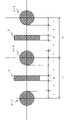
多数の配線経路を実現するため、多層配線基板を構成する各層の配線基板上には多数のビアを配置するが、各ビアは、実装部品等に合わせて、等ピッチの格子状に配置するのが一般的であり、等ピッチ間隔のビアの間に配線を収容させている(図12参照)。 In order to realize a large number of wiring paths, a large number of vias are arranged on each layer of the wiring board that constitutes the multilayer wiring board. is common, and wiring is accommodated between vias at regular intervals (see FIG. 12).
例えば、図13に示すように、ビアパッドの径(ここでは直径2r)が0.5mmであり、配線幅wが0.1mmであり、ビアパッドのピッチ間隔pが0.8mmで、ビアパッド2を配置する場合を考える。この場合、ビアパッドと配線パターンの間に0.05mm以上のクリアランスを確保することが必要であるとすると、ビアパッド2-1及び2-2の間に1本の配線3を設けることになる。
For example, as shown in FIG. 13, the diameter of the via pad (here, diameter 2r) is 0.5 mm, the wiring width w is 0.1 mm, and the pitch interval p of the via pad is 0.8 mm. Consider the case of In this case, if it is necessary to secure a clearance of 0.05 mm or more between the via pad and the wiring pattern, one
近年、実装部品の狭ピッチ化に伴い、各配線基板上に配置する各ビアパッドのピッチ間隔も狭ピッチとなっており、ビアパッド間に収容する配線数を増やすことが難しくなっている。 In recent years, as the pitch of mounted components has become narrower, the pitch between via pads arranged on each wiring board has also become narrower, making it difficult to increase the number of wires accommodated between the via pads.
等ピッチで格子状に配列されたビアパッドの間に配線を収容する際に、配線基板の設計条件によっては、ビアパッドのピッチ間隔にクリアランスがわずかに残っていることがある。そのような場合に、配線収容性を向上させるために、設計者はビアパッドの配置を調整して、配線数を増やすようにしている。 When wiring is accommodated between via pads that are arranged in a grid pattern with an equal pitch, a slight clearance may remain between the via pads depending on the design conditions of the wiring board. In such cases, designers adjust the layout of via pads to increase the number of wires in order to improve the wiring capacity.
従来、ビアパッドの配置を調整する方法として、例えば、特許文献1に記載される技術がある。特許文献1の記載技術は、あるブロック領域にあるビアパッド間の縦方向若しくは横方向のピッチ間隔を長くしたり、短くしたりするものである。
Conventionally, there is a technique described in
また、設計者は、配線収容性を向上させるために、ビアパッドの位置を任意の位置に調整するということも行なっている。 Designers also adjust the positions of via pads to arbitrary positions in order to improve wiring capacity.
しかしながら、上述したように、設計者がビアパッドの位置を任意の位置に調整する方法は、作業効率が悪い。また、ビアパッドの位置を変えることによりビア配置領域が拡大するため、ビア配置領域同士の干渉により実装部品を高密度に配置することが難しくなってしまう。 However, as described above, the method by which the designer adjusts the position of the via pad to an arbitrary position is inefficient. In addition, since the via arrangement area is enlarged by changing the position of the via pad, interference between the via arrangement areas makes it difficult to arrange the mounted components at a high density.
また、特許文献1の記載技術のように、ビアパッド間の縦方向若しくは横方向のピッチ間隔を調整する方法は、縦方向若しくは横方向のいずれかにおいて広い領域と狭い領域とが混在してしまうので、収容する配線数に偏りが生じてしまい、他の配線層への影響が生じ得る。
Moreover, in the method of adjusting the vertical or horizontal pitch between via pads, as in the technique described in
そのため、良好な作業効率性で、ビア配置領域を拡大せずに、縦方向及び横方向共に偏りなく配線収容性を向上させることができる配線基板設計支援装置、配線基板ビア配置方法及び配線基板ビア配置プログラムが求められている。 Therefore, a wiring board design support device, a wiring board via arrangement method, and a wiring board via which can improve the wiring capacity evenly in both the vertical and horizontal directions without enlarging the via arrangement area with good work efficiency. A placement program is needed.
かかる課題を解決するために、第1の本発明に係る配線基板設計支援装置は、配線基板に複数のビアを配置する配線基板設計支援装置において、(1)配線基板に配置させるビア及び配線に関する設計情報を記憶する設計情報記憶手段と、(2)設計情報に基づいて、縦横の間隔を等間隔とした格子点の位置を、縦方向及び横方向に所定の移動量だけ移動させるものであって、当該格子の行毎に格子点の横の移動方向を交互に変え、かつ、当該格子の列毎に格子点の縦の移動方向を交互に変えて、移動後の格子点の位置にビアを配置する配線基板ビア配置手段とを備えることを特徴とする。 In order to solve this problem, a wiring board design aid apparatus according to a first aspect of the present invention provides a wiring board design aid apparatus for arranging a plurality of vias on a wiring board, which includes: (1) vias and wiring to be arranged on the wiring board; (2) a design information storage means for storing design information; and (2) based on the design information, the positions of grid points, which are equally spaced in the vertical and horizontal directions, are moved in the vertical and horizontal directions by a predetermined amount of movement. Then, the direction of horizontal movement of the grid points is alternately changed for each row of the grid and the direction of vertical movement of the grid points is alternately changed for each column of the grid, and vias are formed at the positions of the grid points after movement. wiring board via arrangement means for arranging the .
第2の本発明に係る配線基板ビア配置方法は、配線基板に複数のビアを配置する配線基板設計支援方法において、(1)設計情報記憶手段が、配線基板に配置させるビア及び配線に関する設計情報を記憶し、(2)配線基板ビア配置手段が、設計情報に基づいて、縦横の間隔を等間隔とした格子点の位置を、縦方向及び横方向に所定の移動量だけ移動させるものであって、当該格子の行毎に格子点の横の移動方向を交互に変え、かつ、当該格子の列毎に格子点の縦の移動方向を交互に変えて、移動後の格子点の位置にビアを配置することを特徴とする。 A wiring board via placement method according to a second aspect of the present invention is a wiring board design support method for placing a plurality of vias on a wiring board, wherein: (1) design information storage means stores design information relating to vias and wiring to be placed on the wiring board and (2) the wiring board via placement means moves the positions of the grid points, which are equally spaced in the vertical and horizontal directions, by a predetermined amount of movement in the vertical and horizontal directions, based on the design information. Then, the direction of horizontal movement of the grid points is alternately changed for each row of the grid and the direction of vertical movement of the grid points is alternately changed for each column of the grid, and vias are formed at the positions of the grid points after movement. is characterized by arranging
第3の本発明に係る配線基板ビア配置プログラムは、配線基板に複数のビアを配置する配線基板設計支援プログラムにおいて、配線基板に配置させるビア及び配線に関する設計情報を記憶する設計情報記憶手段を有するコンピュータを、設計情報に基づいて、縦横の間隔を等間隔とした格子点の位置を、縦方向及び横方向に所定の移動量だけ移動させるものであって、当該格子の行毎に格子点の横の移動方向を交互に変え、かつ、当該格子の列毎に格子点の縦の移動方向を交互に変えて、移動後の格子点の位置にビアを配置する配線基板ビア配置手段として機能させることを特徴とする。 A wiring board via placement program according to a third aspect of the present invention is a wiring board design support program for placing a plurality of vias on a wiring board, and has design information storage means for storing design information relating to vias and wiring to be placed on the wiring board. Based on the design information, the positions of the grid points, which are equally spaced in the vertical and horizontal directions, are moved by a predetermined amount in the vertical and horizontal directions. Alternating the horizontal movement direction and alternately changing the vertical movement direction of the grid points for each row of the grid to function as wiring board via placement means for arranging vias at the positions of the grid points after movement. It is characterized by
本発明によれば、良好な作業効率性で、ビア配置領域を拡大せずに、縦方向及び横方向共に偏りなく配線収容性を向上させることができる。 According to the present invention, it is possible to improve the wiring capacity with good work efficiency, without enlarging the via arrangement area, and without bias in both the vertical and horizontal directions.
(A)主たる実施形態
以下では、本発明に係る配線基板設計支援装置、配線基板ビア配置方法及び配線基板ビア配置プログラムの実施形態を、図面を参照しながら詳細に説明する。
(A) Main Embodiments Hereinafter, embodiments of a wiring board design support apparatus, a wiring board via placement method, and a wiring board via placement program according to the present invention will be described in detail with reference to the drawings.
(A-1)実施形態の構成
図2は、この実施形態に係る配線基板設計支援装置のハードウェア構成を示す構成図である。
(A-1) Configuration of Embodiment FIG. 2 is a configuration diagram showing a hardware configuration of a wiring board design support apparatus according to this embodiment.
図2において、この実施形態に係る配線基板設計支援装置10は、主制御部11、外部記憶部12、表示部13、入力部14を有する。
In FIG. 2, the circuit board design support
この実施形態に係る配線基板設計支援装置10のハードウェア構成は、例えば、パーソナルコンピュータなどの汎用コンピュータや、配線基板を設計する専用のCAD(Computer-Aided Design)装置等を適用することができる。また、そのようなコンピュータに、実施形態に係る配線基板ビア配置プログラム11Pをインストールすることにより、配線基板設計支援装置10としての機能を実現するようにしてもよい。いずれの構築方法を採用した場合であっても、例えば、図2に示すようなハードウェア構成を有する。なお、配線基板設計支援装置10は、図2に例示する構成要素に加えて、プリンタ、通信部等が、主制御部11に接続されていてもよい。
For the hardware configuration of the wiring board
主制御部11は、CPUや主メモリやワーキングメモリ等を有し、搭載されている実施形態の配線基板ビア配置プログラム11Pを実行するものである。
The
外部記憶部12は、ハードディスク装置、USBメモリなどの主制御部11外部のメモリが該当し、各種データを格納するものである。外部記憶部12は、例えば、後述する基板設計CADデータ12Aや基板設計CAD用ビア追加配置ファイル22Bを格納する。
The
表示部13は、設計者に対して、ガイダンス情報や設計イメージ情報などを表示出力するためのものである。入力部14は、キーボードやマウス等が該当し、設計者からの入力情報を取込むものである。すなわち、表示部13及び入力部14は、設計者とのマンマシンインタフェースを構成している。
The display unit 13 is for displaying and outputting guidance information, design image information, and the like to the designer. The
図3は、この実施形態の配線基板ビア配置プログラム11Pの機能部(ルーチン)構成を示す説明図である。なお、図3に示す全て又は一部の機能部は、ソフトウェアによる実現方法に限定されず、専用チップなどのハードウェアで実現しても良いものである。 FIG. 3 is an explanatory diagram showing the functional part (routine) configuration of the wiring board via placement program 11P of this embodiment. Note that all or part of the functional units shown in FIG. 3 are not limited to being implemented by software, and may be implemented by hardware such as dedicated chips.
図3において、配線基板ビア配置プログラム11Pは、設計データ読込部111、ビア配置部112、配線設定部113を有する。また、ビア配置部112は、余剰クリアランス算出部41、不足クリアランス算出部42、ビア移動量算出部43、ビア座標算出部44、ビア配置情報出力部45を有する。
In FIG. 3, the wiring board via placement program 11P has a design data reading unit 111, a via placement unit 112, and a
なお、主制御部11が実行する配線基板ビア配置プログラム11Pの各構成要素の処理は、動作の項で詳細に説明する。
The processing of each component of the wiring board via placement program 11P executed by the
(A-2)実施形態の動作
次に、この実施形態に係る配線基板設計支援装置10における配線基板ビア配置処理の動作を、図面を参照しながら詳細に説明する。
(A-2) Operation of Embodiment Next, the operation of wiring board via placement processing in the wiring board
図4は、この実施形態に係る配線基板ビア配置処理を示すフローチャートである。 FIG. 4 is a flow chart showing wiring board via placement processing according to this embodiment.
配線基板設計支援装置10において、配線基板ビアの配置方法が開始すると、主制御部11は、外部記憶部12から、基板設計CADデータを読み取る(S10)。
When the wiring board via arrangement method is started in the wiring board
ここで、主制御部11が外部記憶部12から読み取る基板設計CADデータは、配線基板上に配置するビアと配線の設計に必要な情報とすることができる。例えば、基板設計CADデータは、ビアパッド径情報(この実施形態ではビアパッドの半径;r)、ビアパッドピッチ情報(p)、配線パターン幅情報(w)、クリアランス情報(c)、各ビアの座標情報(x,y)を含むものとする。なお、基板設計CADデータは、上記各種情報に限定されるものではなく、それ以外に、配線基板上面に設ける電子部品配置情報、配線基板下面のパッド情報等を含むようにしてもよい。
Here, the board design CAD data read by the
ビアパッド径情報は、配置するビアが接続するパッド(ビアパッド)の径を示す情報である。例えば、図9は、ビアと当該ビアが接続するパッドとの関係を例示する図である。図9では、ビアVが貫通ビアであり、ビアVが半円球状のパッド21と接続している場合を例示している。この例の場合、ビアパッド径情報は、ビアVが接続しているパッド21の径情報を意味する。なお、この実施形態では、ビアパッド径情報がパッド21の半径rである場合を例示するが、ビアパッドの径情報はパッド21の直径であってもよい。また、ビアパッド径情報は、ビアVが接続しているパッド21の形状等に応じた情報とすることができる。
The via pad diameter information is information indicating the diameter of a pad (via pad) connected to a via to be arranged. For example, FIG. 9 is a diagram illustrating the relationship between vias and pads to which the vias are connected. FIG. 9 illustrates the case where the via V is a through via and is connected to the
ビアパッドピッチ情報は、等ピッチで格子状に配列するビア間の距離である。より具体的には、各ビアパッドの中心位置を結ぶ直線の距離である。 Via pad pitch information is the distance between vias arranged in a grid at equal pitches. More specifically, it is the distance of a straight line connecting the center positions of the via pads.
配線パターン幅情報は、配線の幅長である。 The wiring pattern width information is the width length of the wiring.
各ビアの座標情報は、配線基板上のある領域における、X方向及びY方向に等ピッチで格子状に配置した各ビアの座標情報である。プローブカードの配線基板は円板状であり、例えば円形の中心を原点としたXY座標系で表すことができ、等ピッチで形成した格子状のX方向の線とY方向の線との交点の位置を、各ビアの座標情報とすることができる。 The coordinate information of each via is the coordinate information of each via arranged in a grid pattern with equal pitches in the X direction and the Y direction in a certain area on the wiring board. The wiring board of the probe card is disk-shaped, and can be represented, for example, by an XY coordinate system with the center of the circle as the origin. The position can be the coordinate information of each via.
クリアランス情報は、あるビアパッドと配線との間、若しくは、配線と配線との間で最低限確保しなければならない距離である。この実施形態では、ビアパッドと配線との間のクリアランスと、配線と配線との間のクリアランスとが同じである場合を例示する。しかし、ビアパッドと配線との間のクリアランスと、配線と配線との間のクリアランスが異なる場合であってよい。 The clearance information is the minimum distance that must be secured between a certain via pad and wiring or between wirings. This embodiment exemplifies the case where the clearance between the via pad and the wiring is the same as the clearance between the wirings. However, the clearance between the via pad and the wiring may be different from the clearance between the wirings.
上記のように、ビア配置の決定動作を開始する前に、上記基板設計CADデータが定まっており、主制御部11は、上記基板設計CADデータを外部記憶部12から読み取ることができる。
As described above, the board design CAD data is determined before starting the via placement determination operation, and the
主制御部11が基板設計CADデータを読み取ると、主制御部11は、読み取った基板設計CADデータに基づいて、配線数nのときの余剰クリアランスmの値を算出し(S11)、さらに配線数(n+1)のときの不足クリアランスsの値を算出する(S12)。
When the
[余剰クリアランスmの算出方法]
ここで、配線数nとする場合の余剰クリアランスmの算出方法について、図5及び図6を参照しながら説明する。
[Calculation method of surplus clearance m]
Here, a method of calculating the surplus clearance m when the number of wires is n will be described with reference to FIGS. 5 and 6. FIG.
主制御部11は、基板設計CADデータとして、各ビアパッドの半径r、各配線の幅w、クリアランスc、ビアパッドピッチpを取得し、(1)式に従って、余剰クリアランスmの値を算出する。
m=p-min p
=p-2r-(n×w)-(n+1)c …(1)
The
m = p - min p
=p−2r−(n×w)−(n+1)c (1)
(1)式は、2個のビアパッド2-1及び2-2の間に、n本の配線3を収容したときに、基板設計CADデータにおいて予め設定されているビアパッドピッチpに対するクリアランスの余剰量mを算出する演算式である。ここでは、配線3の数が2本である場合を例示している。
Equation (1) is a clearance surplus with respect to the via pad pitch p preset in the board design CAD data when n wirings 3 are accommodated between the two via pads 2-1 and 2-2. It is an arithmetic expression for calculating the quantity m. Here, the case where the number of
(1)式が意味するところは、ビアパッド2-1又は2-2と配線3との間や、収容する配線3同士の間には、最小限確保しなければならないクリアランスcが必要となる。そのため、ビアパッドと配線又は配線同士の間にクリアランスcを確保した状態で、ビアパッド2-1及び2-2の間にn本の配線3を収容させた場合に、どれだけクリアランスが残っているかを導出している。
Expression (1) means that a minimum clearance c is required between the via pad 2-1 or 2-2 and the
図5に示すように、「min p」は、2個のビアパッド2-1及び2-2の間に、n本の配線3を収容するときに必要な最小ビアパッドピッチの距離である。
As shown in FIG. 5, "min p" is the minimum via pad pitch required to accommodate
(1)式では、予め設定されているビアパッドピッチpから、配線数nとしたときの配線収容に必要な最小ビアパッドピッチmin Pを減算した差分値を、余剰クリアランスmの値としている(図6参照)。 In the formula (1), the difference value obtained by subtracting the minimum via pad pitch min P required to accommodate wiring when the number of wirings is n from the via pad pitch p set in advance is taken as the value of the surplus clearance m ( See Figure 6).
[不足クリアランスsの算出方法]
次に、配線数(n+1)とする場合の不足クリアランスsの算出方法について、図7を参照しながら説明する。
[Calculation method of insufficient clearance s]
Next, a method of calculating the insufficient clearance s when the number of wirings is (n+1) will be described with reference to FIG.
主制御部11は、ビアパッド2-1及び2-2間に収容する配線3の数をインクリメントして、配線数をn+1とする。そして、主制御部11は、各ビアパッドの半径r、各配線の幅w、クリアランスc、ビアパッドピッチpを用いて、(2)式に従って、不足クリアランスsの値を算出する。
s=min p-p
=2r+(n+1)w+(n+2)-p …(2)
The
s = min pp
=2r+(n+1)w+(n+2)-p (2)
(2)式は、(n+1)本の配線を収容したときに、基板設計CADデータにおいて予め設定されているビアパッドピッチpで不足しているクリアランスの不足量を算出する演算式である。つまり、(2)式は、2個のビアパッド2-1及び2-2の間に収容する配線数を増やしたときの不足するクリアランス不足量を導出している。 Expression (2) is an arithmetic expression for calculating the amount of insufficient clearance at the via pad pitch p preset in the board design CAD data when (n+1) wirings are accommodated. In other words, the equation (2) derives the insufficient amount of clearance when the number of wires accommodated between the two via pads 2-1 and 2-2 is increased.
図7に示すように、(2)式では、配線数(n+1)としたときの配線収容に必要な最小ビアパッドピッチmin Pから、予め設定されているビアパッドピッチpを減算した差分値を、不足クリアランスsの値としている。 As shown in FIG. 7, in equation (2), the difference value obtained by subtracting the preset via pad pitch p from the minimum via pad pitch min P required to accommodate wiring when the number of wirings is (n+1) is , the value of the insufficient clearance s.
[余剰クリアランスmと不足クリアランスsとの比較]
主制御部11は、余剰クリアランスmの値と不足クリアランスsの値とを比較する(S13)。
[Comparison between surplus clearance m and insufficient clearance s]
The
そして、余剰クリアランスmの値が不足クリアランスsの値以上である場合(S13)、主制御部11は、不等ピッチで各ビアパッドを配置することができると判断して、S14の処理に移行することができる。つまり、余剰クリアランスmの値が不足クリアランスsの値以上である場合には、主制御部11は、ビアパッドの間にn本の配線3を収容することができる(すなわち、収容配線数を増やせるもの)と判断し、等ピッチの格子状に配置されている各ビアパッドの位置を移動させるようにする。
Then, when the value of the surplus clearance m is equal to or greater than the value of the insufficient clearance s (S13), the
一方、余剰クリアランスmの値が不足クリアランスsの値より小さい場合(s13)、主制御部11は、不等ピットで各ビアパッドを配置することができないと判断して、通常のビアパッドの配置処理を行なう(S16)。
On the other hand, when the value of the surplus clearance m is smaller than the value of the insufficient clearance s (s13), the
[ビア移動量(オフセット量)の算出及び配置]
S13において、余剰クリアランスmの値が不足クリアランスsの値以上である場合、主制御部11は、等ピッチの格子状に配置されている各ビアパッドの位置座標から、X方向及びY方向に移動させるための移動量deltaを算出する(S14)。
[Calculation and Arrangement of Via Movement Amount (Offset Amount)]
In S13, if the value of the surplus clearance m is equal to or greater than the value of the insufficient clearance s, the
そして、主制御部11は、等ピッチの格子状に配置されている各ビアパッドの位置座標(すなわち、x座標値、y座標値のそれぞれ)に、移動量deltaを加算又は減算して、不等ピッチの各ビアパッドの位置座標(x座標値、y座標値)を算出する(S15)。これにより、等ピッチの格子状に配置されていた各ビアパッドを、不等ピッチに配置することができる(S15)。
Then, the
ここで、図1、図8を参照しながら、主制御部11によるビアパッドの移動量deltaの算出方法及び各ビアパッドの配置方法を説明する。
Here, a method of calculating the movement amount delta of the via pad and a method of arranging each via pad by the
主制御部11は、余剰クリアランスmの値と不足クリアランスsの値とを用いて、(3)式に従い各ビアパッドの移動量deltaを算出する。
s/2≦ delta ≦m/2 …(3)
The
s/2≤delta≤m/2 (3)
(3)式より、各ビアパッドの移動量deltaの値を、不足クリアランスsの値の1/2以上であり、余剰クリアランスmの値の1/2以下とする。移動量deltaの値は、上記(3)式の条件を満たしていれば、任意の値とすることができる。 (3), the value of the movement amount delta of each via pad is set to 1/2 or more of the value of the insufficient clearance s and 1/2 or less of the value of the surplus clearance m. The value of the movement amount delta can be any value as long as the condition of the above formula (3) is satisfied.
移動量deltaは、上述したように、等ピッチの格子点にある各ビアパッドの位置座標から、X方向の移動量及びY方向の移動量であり、この実施形態では、X方向の移動量とY方向の移動量とが同じとする。すなわち、各ビアパッドは、X方向に移動量deltaだけ移動し、かつ、Y方向に移動量deltaだけ移動する。このように、X方向の移動量とY方向の移動量は同じ移動量としており、その移動後の位置が配置調整後のビアの位置となる。 The amount of movement delta is, as described above, the amount of movement in the X direction and the amount of movement in the Y direction from the positional coordinates of each via pad at lattice points at equal pitches. The amount of movement in the direction is assumed to be the same. That is, each via pad moves in the X direction by the movement amount delta and moves in the Y direction by the movement amount delta. Thus, the amount of movement in the X direction and the amount of movement in the Y direction are the same, and the position after the movement is the position of the via after the placement adjustment.
また、図8に示すように、等ピッチの格子点にある各ビアパッドの位置座標からの移動方向は、X方向、Y方向共に、移動量deltaを移動させる方向を交互に変える。 Further, as shown in FIG. 8, the direction of movement from the positional coordinates of each via pad at grid points with equal pitch alternates in both the X direction and the Y direction to move the movement amount delta.
換言すると、X方向に関する移動方向は、格子状に配列しているビアパッドのうち、同一の行に属しているビアパッドについては、「-方向」に移動量deltaだけ移動させ、当該行に隣接している行に属しているビアパッドについては、「+方向」に移動量deltaだけ移動させる。このように、ビアパッドのX方向の移動については、行毎に、交互に移動させる方向を変えて、X座標値から移動量deltaだけ移動させる。 In other words, regarding the movement direction in the X direction, of the via pads arranged in a grid pattern, the via pads belonging to the same row are moved in the “− direction” by the movement amount delta, and are moved adjacent to the row. The via pad belonging to the current row is moved in the "+ direction" by the movement amount delta. As described above, the via pad is moved in the X direction by changing the direction of movement alternately for each row, and moving the via pad by the movement amount delta from the X coordinate value.
またY方向に関する移動方向も、X方向の移動と同様とする。すなわち、格子状に配列しているビアパッドのうち、同一の列に属しているビアパッドについては、「-方向」に移動量deltaだけ移動させ、当該列に隣接している列に属しているビアパッドについては、「+方向」に移動量deltaだけ移動させる。このように、ビアパッドのY方向の移動については、列毎に、交互に移動させる方向を変えて、Y座標値から移動量deltaだけ移動させる。 Also, the direction of movement in the Y direction is the same as the movement in the X direction. That is, of the via pads arranged in a grid pattern, the via pads belonging to the same row are moved in the "- direction" by the movement amount delta, and the via pads belonging to the row adjacent to the row are moved. moves in the "+ direction" by the movement amount delta. In this manner, the via pads are moved in the Y direction by changing the direction of movement alternately for each column, and moving the via pads by the movement amount delta from the Y coordinate value.
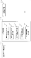
上述したように、各ビアパッドのX方向、Y方向のそれぞれについて、移動方向を交互に変えながら、移動量deltaだけ移動させることにより、図1に例示するように、等ピッチで格子状に配置していた各ビアパッド2は、不等ピッチで配置されることになる。
As described above, each of the via pads in the X direction and the Y direction is moved by the movement amount delta while alternately changing the movement direction. The via
[配線の設定]
主制御部11は、不等ピッチで各ビアパッド2が配置されると、ビアパッド2の間に配線3を設定する。
[Wiring settings]
When the via
ここで、図1、図10及び図11と図13とを用いて、等ピッチのビアパッド2(2-1及び2-2)間に配線3を設定する場合と、不等ピッチのビアパッド2(2-1及び2-2)間に配線3を設定する場合とを比較しながら説明する。
Here, referring to FIGS. 1, 10, 11 and 13, a case of setting
なお、ビアパッド2(2-1及び2-2)の半径rが0.5mmであり、配線幅wが0.1mmであり、ビアパッド2と配線3との間若しくは配線間に0.05mm以上のクリアランスcを確保することが必要であるものとする。
The radius r of the via pad 2 (2-1 and 2-2) is 0.5 mm, the wiring width w is 0.1 mm, and the distance between the via
図13に示すように、等ピッチであるビアパッドピッチ間隔pが0.8mmの場合、ビアパッド2-1及び2-2の間には1本の配線3のみを収容可能である。
As shown in FIG. 13, when the uniform via pad pitch interval p is 0.8 mm, only one
これに対して、図1に示すように、例えば移動量deltaを0.05mmとして、各ビアパッド2の位置座標を移動させて、不等ピッチにビアパッド2を配置したとする。
On the other hand, as shown in FIG. 1, it is assumed that the position coordinates of each via
この場合、図11に示すように、ビアパッド2-1とビアパッド2-2との間のビアパッドピッチ間隔p1は0.9mmとなるので、ビアパッド2-1及び2-2の間には2本の配線3を収容することができる。一方、ビアパッド2-2とビアパッド2-3との間のビアパッドピッチ間隔p2は0.7mmとなるので、ビアパッド2-2及び2-3の間には1本の配線3を収容することができる(図10参照)。
In this case, as shown in FIG. 11, the via pad pitch interval p1 between the via pads 2-1 and 2-2 is 0.9 mm. of
このように、各ビアパッド2が不等ピッチで配置されることにより、隣接するビアパッド2との間のピッチ間隔が拡がる領域と、逆に隣接するビアパッド2のピッチ間隔が狭くなる領域とが生じる。従って、主制御部11は、図10、図11に示すように、ピッチ間隔が拡がった領域では、収容配線数を増やして、配線3を収容することができる。
By arranging the via
また、ビアの位置を移動させる移動量deltaの値は、上記(3)式のように、不足クリアランスsの値の1/2以上であり、余剰クリアランスmの値の1/2以下とするため、ピッチ間隔が狭くなった領域においても、等ピッチでビアパッド2を配置したときと同数の配線3を収容することができる。
Further, the value of the movement amount delta for moving the position of the via is, as in the above equation (3), 1/2 or more of the value of the insufficient clearance s and 1/2 or less of the value of the surplus clearance m. , the same number of
(A-3)実施形態の効果
以上のように、この実施形態によれば、等ピッチで格子状に配置されたビアパッドの位置座標にオフセット量としての移動量を加算又は減算して、不等ピッチのビアパッドを配置しているので、ビア配置領域を拡大させずに、縦方向、横方向共に、偏りなく配線収容性を向上させることができる。
(A-3) Effect of Embodiment As described above, according to this embodiment, a movement amount as an offset amount is added to or subtracted from the position coordinates of via pads arranged in a grid pattern at an equal pitch, and unequal Since the via pads are arranged at a pitch, it is possible to improve the wiring capacity evenly in both the vertical and horizontal directions without increasing the via arrangement area.
また、実施形態によれば、予め規則性のある不等ピッチでビアパッドを配置しているので、作業効率性も良い。 Moreover, according to the embodiment, since the via pads are arranged in advance at irregular pitches with regularity, work efficiency is also good.
さらに、実施形態によれば、配線収容性が向上するため、多層配線基板は、層数削減が期待でき、配線基板の製造コストの削減も可能となる。 Furthermore, according to the embodiment, since the wiring capacity is improved, the number of layers in the multilayer wiring board can be expected to be reduced, and the manufacturing cost of the wiring board can be reduced.
(B)他の実施形態
上述した実施形態においても種々の変形実施形態を言及したが、本発明は、以下の変形実施形態にも適用することができる。
(B) Other Embodiments Although various modified embodiments have been mentioned in the embodiments described above, the present invention can also be applied to the following modified embodiments.
(B-1)上述した実施形態では、ビアの配置方法を例示して説明した。しかし、例えばBGA(Ball Grid Array)等のように、ピッチで複数の電子部品を搭載する配線基板において、等ピッチで、一列以上、配列している上記各電子部品の端子の位置を配置する場合にも適用できる。つまり、ビアの配置に限定されるものではなく、電子部品の端子の配置としてもよいし、又等ピッチに配列されていれば、格子状に配置されていることに限定されるものではない。 (B-1) In the above-described embodiments, the method of arranging vias has been exemplified. However, in a wiring board on which a plurality of electronic components are mounted at a pitch, such as a BGA (Ball Grid Array), when arranging the positions of the terminals of the electronic components arranged in one or more rows at an equal pitch, can also be applied to In other words, the arrangement is not limited to the arrangement of vias, but may be the arrangement of terminals of electronic components, and is not limited to being arranged in a grid as long as they are arranged at equal pitches.
(B-2)上述した実施形態において、余剰クリアランスの算出方法、不足クリアランスの算出方法は、上記の限定されるものではない。 (B-2) In the above-described embodiment, the method of calculating the surplus clearance and the method of calculating the insufficient clearance are not limited to those described above.
2(2-1~2-3)、21,22…ビアパッド、3…配線パターン、
10…配線基板設計支援装置、11…主制御部、12…外部記憶部、13…表示部、14…入力部、11P…配線基板ビア配置プログラム、111…設計データ読込部、112…ビア配置部、113…配線設定部、41…余剰クリアランス算出部、42…不足クリアランス算出部、43…ビア移動量算出部、44…ビア座標算出部、45…ビア配置情報出力部。
2 (2-1 to 2-3), 21, 22... via pads, 3... wiring patterns,
DESCRIPTION OF
Claims (5)
上記配線基板に配置させるビア及び配線に関する設計情報を記憶する設計情報記憶手段と、
上記設計情報に基づいて、縦横の間隔を等間隔とした格子点の位置を、縦方向及び横方向に所定の移動量だけ移動させるものであって、当該格子の行毎に上記格子点の横の移動方向を交互に変え、かつ、当該格子の列毎に上記格子点の縦の移動方向を交互に変えて、移動後の上記格子点の位置にビアを配置する配線基板ビア配置手段と
を備えることを特徴とする配線基板設計支援装置。 In a wiring board design support device for arranging a plurality of vias on a wiring board,
design information storage means for storing design information about vias and wiring to be arranged on the wiring board;
Based on the design information, the positions of the grid points, which are equally spaced in the vertical and horizontal directions, are moved in the vertical and horizontal directions by a predetermined amount of movement. and wiring board via placement means for alternately changing the moving direction of the grid points and alternately changing the vertical moving direction of the grid points for each row of the grid to place vias at the positions of the grid points after movement. A wiring board design support device, comprising:
上記設計情報に基づいて、上記縦横の間隔が等間隔とした格子点の位置にビアを配置して、ビア間に配線を配置したときの余剰クリアランスの値を求める余剰クリアランス算出部と、
上記ビア間に、上記配線の数を増やして上記配線を配置したとき不足クリアランスの値を求める不足クリアランス算出部と、
上記余剰クリアランスの値と上記不足クリアランスの値との比較結果に応じて、上記格子点の位置を縦方向及び横方向に移動させる移動量を算出する移動量算出部と
を有することを特徴とする請求項1に記載の配線基板設計支援装置。 The wiring board via placement means includes:
a surplus clearance calculation unit that calculates a value of surplus clearance when wiring is arranged between the vias by arranging the vias at the positions of the grid points with the equal intervals in the vertical and horizontal directions based on the design information;
an insufficient clearance calculation unit that obtains a value of insufficient clearance when increasing the number of the wirings and arranging the wirings between the vias;
a movement amount calculation unit that calculates a movement amount for moving the position of the grid point in the vertical direction and the horizontal direction according to a comparison result between the value of the excess clearance and the value of the insufficient clearance. 2. The wiring board design support device according to claim 1.
設計情報記憶手段が、上記配線基板に配置させるビア及び配線に関する設計情報を記憶し、
配線基板ビア配置手段が、上記設計情報に基づいて、縦横の間隔を等間隔とした格子点の位置を、縦方向及び横方向に所定の移動量だけ移動させるものであって、当該格子の行毎に上記格子点の横の移動方向を交互に変え、かつ、当該格子の列毎に上記格子点の縦の移動方向を交互に変えて、移動後の上記格子点の位置にビアを配置する
ことを特徴とする配線基板ビア配置方法。 In a wiring board via arrangement method for arranging a plurality of vias on a wiring board,
design information storage means stores design information about vias and wiring to be arranged on the wiring board;
Wiring board via placement means moves the positions of grid points, which are equally spaced in the vertical and horizontal directions, by a predetermined amount of movement in the vertical and horizontal directions based on the design information. alternately changing the horizontal movement direction of the lattice points for each column of the lattice, and alternately changing the vertical movement direction of the lattice points for each row of the lattice, and arranging the vias at the positions of the lattice points after movement. A wiring board via arrangement method characterized by:
上記配線基板に配置させるビア及び配線に関する設計情報を記憶する設計情報記憶手段を有するコンピュータを、
上記設計情報に基づいて、縦横の間隔を等間隔とした格子点の位置を、縦方向及び横方向に所定の移動量だけ移動させるものであって、当該格子の行毎に上記格子点の横の移動方向を交互に変え、かつ、当該格子の列毎に上記格子点の縦の移動方向を交互に変えて、移動後の上記格子点の位置にビアを配置する配線基板ビア配置手段
として機能させることを特徴とする配線基板ビア配置プログラム。 In a wiring board via placement program for arranging a plurality of vias on a wiring board,
a computer having design information storage means for storing design information relating to vias and wiring to be arranged on the wiring board;
Based on the design information, the positions of the grid points, which are equally spaced in the vertical and horizontal directions, are moved in the vertical and horizontal directions by a predetermined amount of movement. and alternately change the vertical movement direction of the grid points for each row of the grid to place vias at the positions of the grid points after movement. A wiring board via placement program characterized by:
Priority Applications (5)
| Application Number | Priority Date | Filing Date | Title |
|---|---|---|---|
| JP2018152509A JP7123692B2 (en) | 2018-08-13 | 2018-08-13 | Wiring board design support device, wiring board via placement method, and wiring board via placement program |
| US16/454,441 US10776556B2 (en) | 2018-08-13 | 2019-06-27 | Wiring board design support apparatus, method for wiring board via arrangement and storage medium recording program for wiring board via arrangement |
| TW108123535A TWI724447B (en) | 2018-08-13 | 2019-07-04 | Wiring board design support device, wiring board through hole placement method and wiring board through hole placement program |
| KR1020190085240A KR102289322B1 (en) | 2018-08-13 | 2019-07-15 | Wiring Board Design Support Apparatus, Method for Wiring Board Via Arrangement and Program for Wiring Board Via Arrangement |
| CN201910744180.7A CN110874518B (en) | 2018-08-13 | 2019-08-13 | Design support device for wiring substrate, via arrangement method, and recording medium |
Applications Claiming Priority (1)
| Application Number | Priority Date | Filing Date | Title |
|---|---|---|---|
| JP2018152509A JP7123692B2 (en) | 2018-08-13 | 2018-08-13 | Wiring board design support device, wiring board via placement method, and wiring board via placement program |
Publications (2)
| Publication Number | Publication Date |
|---|---|
| JP2020027487A JP2020027487A (en) | 2020-02-20 |
| JP7123692B2 true JP7123692B2 (en) | 2022-08-23 |
Family
ID=69406146
Family Applications (1)
| Application Number | Title | Priority Date | Filing Date |
|---|---|---|---|
| JP2018152509A Active JP7123692B2 (en) | 2018-08-13 | 2018-08-13 | Wiring board design support device, wiring board via placement method, and wiring board via placement program |
Country Status (5)
| Country | Link |
|---|---|
| US (1) | US10776556B2 (en) |
| JP (1) | JP7123692B2 (en) |
| KR (1) | KR102289322B1 (en) |
| CN (1) | CN110874518B (en) |
| TW (1) | TWI724447B (en) |
Families Citing this family (4)
| Publication number | Priority date | Publication date | Assignee | Title |
|---|---|---|---|---|
| US11901286B2 (en) * | 2021-01-28 | 2024-02-13 | Taiwan Semiconductor Manufacturing Company, Ltd. | Diagonal via pattern and method |
| CN112949244B (en) * | 2021-03-29 | 2022-12-13 | 福建福强精密印制线路板有限公司 | Intelligent nail selecting method and storage medium |
| CN114340175A (en) * | 2022-01-10 | 2022-04-12 | 鹤山市泰利诺电子有限公司 | Circuit board routing method |
| CN117320268A (en) * | 2022-06-21 | 2023-12-29 | 中兴智能科技南京有限公司 | Circuit board and circuit board assembly |
Citations (3)
| Publication number | Priority date | Publication date | Assignee | Title |
|---|---|---|---|---|
| JP2002334124A (en) | 2001-05-11 | 2002-11-22 | Nec Corp | Device and method for adjusting wiring width in printed wiring board |
| US7269813B2 (en) | 2004-11-19 | 2007-09-11 | Alcatel | Off-width pitch for improved circuit card routing |
| WO2009122494A1 (en) | 2008-03-31 | 2009-10-08 | 富士通株式会社 | Wiring board design support device, wiring board design support method, wiring board design support program, and computer-readable recording medium having the program recorded |
Family Cites Families (29)
| Publication number | Priority date | Publication date | Assignee | Title |
|---|---|---|---|---|
| JPH06140751A (en) * | 1992-10-28 | 1994-05-20 | Matsushita Electric Works Ltd | Method for lead wire soldering onto printed-wiring board |
| US6510539B1 (en) * | 1999-10-29 | 2003-01-21 | International Business Machines Corporation | System and method for physically modeling electronic modules wiring |
| JP3786398B2 (en) * | 2000-09-07 | 2006-06-14 | 新光電気工業株式会社 | Wiring method of semiconductor package |
| US6762366B1 (en) * | 2001-04-27 | 2004-07-13 | Lsi Logic Corporation | Ball assignment for ball grid array package |
| WO2008095091A2 (en) * | 2007-01-31 | 2008-08-07 | Nanonexus, Inc. | Structures and processes for fabrication of probe card assemblies with multi-layer interconnect |
| US7624367B2 (en) * | 2002-11-18 | 2009-11-24 | Cadence Design Systems, Inc. | Method and system for routing |
| US7007258B2 (en) * | 2003-06-13 | 2006-02-28 | Sun Microsystems, Inc. | Method, apparatus, and computer program product for generation of a via array within a fill area of a design layout |
| US7738259B2 (en) * | 2004-01-22 | 2010-06-15 | Alcatel Lucent | Shared via decoupling for area arrays components |
| JP4528024B2 (en) * | 2004-04-28 | 2010-08-18 | 富士通株式会社 | Program for executing circuit analysis method |
| US7340711B2 (en) * | 2004-06-04 | 2008-03-04 | Cadence Design Systems, Inc. | Method and apparatus for local preferred direction routing |
| US7323787B2 (en) * | 2005-01-25 | 2008-01-29 | Alcatel | Off-grid decoupling of ball grid array (BGA) devices and method |
| JP2007041867A (en) * | 2005-08-03 | 2007-02-15 | Elpida Memory Inc | Inductance analysis system, method and program |
| US7368667B2 (en) * | 2005-08-10 | 2008-05-06 | Alcatel | Using rows/columns of micro-vias to create PCB routing channels in BGA interconnect grid (micro-via channels) |
| JP4270210B2 (en) | 2006-01-20 | 2009-05-27 | セイコーエプソン株式会社 | Circuit board, bumped semiconductor element mounting structure, electro-optical device, and electronic device |
| US7464358B1 (en) * | 2006-01-26 | 2008-12-09 | Cadence Design Systems, Inc. | Method for resolving overloads in autorouting physical interconnections |
| TWI319298B (en) * | 2007-03-19 | 2010-01-01 | Inventec Corp | Via-adjusting method and system |
| US7797663B2 (en) * | 2007-04-04 | 2010-09-14 | Cisco Technology, Inc. | Conductive dome probes for measuring system level multi-GHZ signals |
| TWI330798B (en) * | 2007-05-01 | 2010-09-21 | Inventec Corp | Method for designing printed circuit board |
| JP5223790B2 (en) * | 2009-06-22 | 2013-06-26 | 富士通株式会社 | Printed circuit board design support program, printed circuit board design support method, and printed circuit board design support apparatus |
| JP5212296B2 (en) * | 2009-07-22 | 2013-06-19 | 富士通株式会社 | Wiring design support device, wiring design support method, and wiring design support program |
| JP5459543B2 (en) * | 2009-12-04 | 2014-04-02 | 日本電気株式会社 | Circuit board and design method thereof |
| JP2012038043A (en) * | 2010-08-05 | 2012-02-23 | Sharp Corp | Wiring design support device, wiring design support method, and wiring design support program |
| US9627306B2 (en) * | 2012-02-15 | 2017-04-18 | Cypress Semiconductor Corporation | Ball grid structure |
| JP5779145B2 (en) * | 2012-06-28 | 2015-09-16 | 株式会社Screenホールディングス | Wiring data generation device, generation method, program thereof, and drawing device |
| JP6249340B2 (en) * | 2013-02-07 | 2017-12-20 | パナソニックIpマネジメント株式会社 | ORGANIC ELECTROLUMINESCENT ELEMENT AND LIGHTING DEVICE |
| JP6234797B2 (en) * | 2013-12-06 | 2017-11-22 | 株式会社日本マイクロニクス | Wiring board via arrangement determination apparatus, method and program |
| US9898567B2 (en) * | 2014-02-28 | 2018-02-20 | Synopsys, Inc. | Automatic layout modification tool with non-uniform grids |
| KR20160096249A (en) * | 2015-02-04 | 2016-08-16 | 삼성전자주식회사 | System for verifying design |
| US9635760B1 (en) * | 2016-01-19 | 2017-04-25 | Alcatel-Lucent Usa Inc. | 0204 shifted vias with merge pads |
-
2018
- 2018-08-13 JP JP2018152509A patent/JP7123692B2/en active Active
-
2019
- 2019-06-27 US US16/454,441 patent/US10776556B2/en active Active
- 2019-07-04 TW TW108123535A patent/TWI724447B/en active
- 2019-07-15 KR KR1020190085240A patent/KR102289322B1/en active IP Right Grant
- 2019-08-13 CN CN201910744180.7A patent/CN110874518B/en active Active
Patent Citations (3)
| Publication number | Priority date | Publication date | Assignee | Title |
|---|---|---|---|---|
| JP2002334124A (en) | 2001-05-11 | 2002-11-22 | Nec Corp | Device and method for adjusting wiring width in printed wiring board |
| US7269813B2 (en) | 2004-11-19 | 2007-09-11 | Alcatel | Off-width pitch for improved circuit card routing |
| WO2009122494A1 (en) | 2008-03-31 | 2009-10-08 | 富士通株式会社 | Wiring board design support device, wiring board design support method, wiring board design support program, and computer-readable recording medium having the program recorded |
Also Published As
| Publication number | Publication date |
|---|---|
| JP2020027487A (en) | 2020-02-20 |
| KR20200019080A (en) | 2020-02-21 |
| CN110874518A (en) | 2020-03-10 |
| TW202018301A (en) | 2020-05-16 |
| KR102289322B1 (en) | 2021-08-11 |
| CN110874518B (en) | 2023-09-08 |
| TWI724447B (en) | 2021-04-11 |
| US10776556B2 (en) | 2020-09-15 |
| US20200050732A1 (en) | 2020-02-13 |
Similar Documents
| Publication | Publication Date | Title |
|---|---|---|
| JP7123692B2 (en) | Wiring board design support device, wiring board via placement method, and wiring board via placement program | |
| US20060136848A1 (en) | Cell, standard cell, standard cell library, a placement method using standard cell, and a semiconductor integrated circuit | |
| JP2009223885A (en) | Method of designing printed circuit board, and design support apparatus of printed circuit board | |
| JPH0969568A (en) | Method for arranging and wiring flip-chip-type semiconductor device | |
| KR101824780B1 (en) | Method and system for diagnosing a semiconductor wafer | |
| US7698679B2 (en) | Method and apparatus for automatic routing yield optimization | |
| JP2013037451A (en) | Layout design device, layout design method, and layout design program | |
| JP2006253187A (en) | Power source analyzing method and program for analyzing power source analysis | |
| US7884629B2 (en) | Probe card layout | |
| US20150324507A1 (en) | Printed circuit board design verification system, printed circuit board design verification method, and recording medium | |
| US20090013298A1 (en) | Offset Fill | |
| US9760670B2 (en) | Semiconductor device design methods and conductive bump pattern enhancement methods | |
| JP5136333B2 (en) | Power noise analysis model creation method, power noise analysis model creation device, and power noise analysis model creation program | |
| US20120047472A1 (en) | Dummy-metal-layout evaluating device and dummy-metal-layout evaluating method | |
| US11901223B2 (en) | Stress analysis method and semiconductor device manufacturing method | |
| JP3589931B2 (en) | Layout method of semiconductor integrated circuit | |
| JP2012023278A (en) | Semiconductor device and method of manufacturing semiconductor device | |
| US20070033563A1 (en) | Method of semiconductor device and design supporting system of semiconductor device | |
| JP2006294707A (en) | Semiconductor integrated circuit and method of wiring the same | |
| JP4943918B2 (en) | Real shape verification device | |
| JP2008282214A (en) | Printed circuit board design device, printed circuit board design method, and printed circuit board design program | |
| US20070131647A1 (en) | Semiconductor device and support method for designing the same | |
| JP2017162336A (en) | Board design device and board design method | |
| US20170023616A1 (en) | Interdigitized polysymmetric fanouts, and associated systems and methods | |
| JP2012083952A (en) | Layout design device, layout design method, and program |
Legal Events
| Date | Code | Title | Description |
|---|---|---|---|
| A621 | Written request for application examination |
Free format text: JAPANESE INTERMEDIATE CODE: A621 Effective date: 20210805 |
|
| A977 | Report on retrieval |
Free format text: JAPANESE INTERMEDIATE CODE: A971007 Effective date: 20220624 |
|
| TRDD | Decision of grant or rejection written | ||
| A01 | Written decision to grant a patent or to grant a registration (utility model) |
Free format text: JAPANESE INTERMEDIATE CODE: A01 Effective date: 20220712 |
|
| A61 | First payment of annual fees (during grant procedure) |
Free format text: JAPANESE INTERMEDIATE CODE: A61 Effective date: 20220810 |
|
| R150 | Certificate of patent or registration of utility model |
Ref document number: 7123692 Country of ref document: JP Free format text: JAPANESE INTERMEDIATE CODE: R150 |