JP7121971B2 - Three-phase AC-DC converter - Google Patents
Three-phase AC-DC converter Download PDFInfo
- Publication number
- JP7121971B2 JP7121971B2 JP2018053681A JP2018053681A JP7121971B2 JP 7121971 B2 JP7121971 B2 JP 7121971B2 JP 2018053681 A JP2018053681 A JP 2018053681A JP 2018053681 A JP2018053681 A JP 2018053681A JP 7121971 B2 JP7121971 B2 JP 7121971B2
- Authority
- JP
- Japan
- Prior art keywords
- phase
- converter
- switch
- power supply
- circuit
- Prior art date
- Legal status (The legal status is an assumption and is not a legal conclusion. Google has not performed a legal analysis and makes no representation as to the accuracy of the status listed.)
- Active
Links
Images


Classifications
-
- Y—GENERAL TAGGING OF NEW TECHNOLOGICAL DEVELOPMENTS; GENERAL TAGGING OF CROSS-SECTIONAL TECHNOLOGIES SPANNING OVER SEVERAL SECTIONS OF THE IPC; TECHNICAL SUBJECTS COVERED BY FORMER USPC CROSS-REFERENCE ART COLLECTIONS [XRACs] AND DIGESTS
- Y02—TECHNOLOGIES OR APPLICATIONS FOR MITIGATION OR ADAPTATION AGAINST CLIMATE CHANGE
- Y02B—CLIMATE CHANGE MITIGATION TECHNOLOGIES RELATED TO BUILDINGS, e.g. HOUSING, HOUSE APPLIANCES OR RELATED END-USER APPLICATIONS
- Y02B70/00—Technologies for an efficient end-user side electric power management and consumption
- Y02B70/10—Technologies improving the efficiency by using switched-mode power supplies [SMPS], i.e. efficient power electronics conversion e.g. power factor correction or reduction of losses in power supplies or efficient standby modes
Description
本発明は、三相交流(三相AC)を直流(DC)に変換する三相AC-DCコンバータに関するものである。 The present invention relates to a three-phase AC-DC converter that converts three-phase alternating current (three-phase AC) to direct current (DC).
太陽光発電などの分散電源、鉄道・船舶などの輸送交通用電源、またデータセンターなどの情報通信用電源では、CO2削減のために大型の低周波トランスではなく、小型な高周波トランスの適用が進む傾向であり、特に、中圧交流(例えば、3.3kV,6.6kV)から低圧直流(400~700V)を生成する電源では、パワー半導体素子のスイッチングに基づき交流を変換する高周波リンク電力変圧器(Solid State Transformer;SST)が有用である。SSTは高周波でトランスを励磁するため、従来の変圧器と比較して大幅な小型化が可能である。しかし現状では、電力変換段数の増加やパワー半導体素子での電力損失、電力制御手段の複雑化などが要因で実用レベルに至っておらず、SSTの更なる小型軽量化と電力変換効率の向上(高効率化)が期待されている。 Distributed power sources such as solar power generation, transportation power sources such as railroads and ships, and information and communication power sources such as data centers use small high-frequency transformers instead of large low-frequency transformers to reduce CO2 emissions. In particular, in power supplies that generate low-voltage DC (400-700V) from medium-voltage AC (e.g., 3.3 kV, 6.6 kV), high-frequency link power transformers that convert AC based on the switching of power semiconductor elements A solid state transformer (SST) is useful. Since the SST excites the transformer at a high frequency, it can be made much smaller than conventional transformers. However, at present, due to factors such as an increase in the number of power conversion stages, power loss in power semiconductor devices, and the complication of power control means, it has not yet reached a practical level. efficiency) is expected.
電力変換段数に関しては、低周波交流から直流へ変換(三相AC-DC変換)、直流を昇圧変換および力率改善(DC-DC昇圧変換)、直流から高周波交流へ変換(DC-AC変換)、高周波交流から直流に変換(AC-DC変換)といった複数段変換をより簡略化すべきことが要求されている。特に、低周波から高周波を生成する3段変換プロセスを1段まで削減することにより、2~3%の電力損失の改善が図れると言われている。
また、SSTデバイス全体の体積増化と重量増化およびメンテナンス頻度増化の要因である大容量の電力フィルタを用いない回路方式の導入は、小型軽量化にとって重要であり、低コスト化が図れる。また、パワー半導体素子の高速スイッチング動作に関して、低損失化、低ノイズ化を実現するソフトスイッチング技術が必要であり、それに適する電力制御として高周波パルス変調制御の導入が重要である。加えて、実用性の観点から、技術的に未成熟な自励式双方スイッチを使用しない回路方式がのぞましい。更に、国内外の三相電源の結線方式の違いや、用途に応じて多重化や直並列化ができる拡張性が必要である。
Regarding the number of power conversion stages, low-frequency AC to DC conversion (three-phase AC-DC conversion), DC step-up conversion and power factor improvement (DC-DC step-up conversion), and DC to high-frequency AC conversion (DC-AC conversion). , high-frequency alternating current to direct current (AC-DC conversion) should be simplified more. In particular, it is said that a 2-3% improvement in power loss can be achieved by reducing the three-stage conversion process for generating high frequencies from low frequencies to one stage.
In addition, the introduction of a circuit system that does not use a large-capacity power filter, which is a factor in increasing the volume and weight of the entire SST device and increasing the frequency of maintenance, is important for miniaturization and weight reduction, and costs can be reduced. In addition, regarding the high-speed switching operation of power semiconductor devices, a soft-switching technique that achieves low loss and low noise is required, and the introduction of high-frequency pulse modulation control as suitable power control is important. In addition, from the viewpoint of practicality, a circuit system that does not use a technically immature self-excited double-sided switch is desirable. Furthermore, it is necessary to have expandability that allows multiplexing and series-parallelization according to differences in wiring methods of three-phase power sources in Japan and overseas, and applications.
三相交流電圧から直流電圧に変換する従来例としては、例えば特許文献1に電源装置(図22を参照)が開示されている。特許文献1の電源装置は、三相AC-DC変換、DC-DC昇圧変換、DC-AC変換、AC-DC変換と何段階も経た変換を行うために、電力変換効率が低下するという問題を有している。すなわち、高周波トランスの1次側が低周波交流から直流、直流の昇圧、直流から高周波交流の3段変換のため、損失が大きく、また部品数も多くなる。すなわち、多段変換ゆえにパワートランジスタ、インダクタやキャパシタなど回路部品点数の増加による電力変換効率の低下、回路部品コストの増加という問題がある。また、平滑直流リンクを形成する平滑コンデンサ(図22に示すC1,C2)は、通常、大容量アルミ電解コンデンサ等を利用するため、重量が大きくなり、メンテナンス頻度も多くなり、デバイスの小型化と同時に長寿化を阻害するという問題がある。
As a conventional example for converting a three-phase AC voltage to a DC voltage, for example,
また、三相交流電圧を単相交流電圧して単相交流を直流に変換する従来例としては、例えば特許文献2にAC-DCコンバータ(図23を参照)が開示されている。特許文献2にAC-DCコンバータは、3相-単相マトリクスコンバータという回路構成を用い、6個の双方向スイッチを用いて三相交流電圧を単相交流電圧に変換している。しかしながら、双方向スイッチは、デバイスの信頼性が低く、耐圧の高い素子が未開発で、また、転流時に素子の破壊を起こす等の問題を有しており、商業的な利用が困難な状況にある。また、特許文献2にAC-DCコンバータでは、正弦波-三角波比較方式や空間ベクトル変調等の電力制御手法を適用しているために、変調度分解能の制限や制御演算処理の複雑化の恐れがあり、高周波化が困難である。
As a conventional example of converting a three-phase AC voltage into a single-phase AC voltage and converting the single-phase AC into a DC, for example,
上記状況に鑑みて、本発明は、三相交流電源から入力する低周波交流を1段の回路構成にて高周波交流に変換することにより、電力損失を少なく、部品点数も減らし、電力変換効率の向上を図ることができる三相AC-DCコンバータを提供することを目的とする。
商用周波の三相交流電源が接続されたHFトランス1次側コンバータは、各相電力制御回路(Phase modular構造)であり、用途に応じてその2次側は直列または並列接続とする。このため、電源の2倍周波成分をもつ電力脈動をキャンセルし、直流出力端における電圧脈動を効果的に抑制した三相AC-DCコンバータを提供する。
In view of the above situation, the present invention converts low-frequency AC input from a three-phase AC power supply into high-frequency AC in a single-stage circuit configuration, thereby reducing power loss, reducing the number of parts, and improving power conversion efficiency. It is an object of the present invention to provide an improved three-phase AC-DC converter.
An HF transformer primary side converter connected to a commercial frequency three-phase AC power supply is a power control circuit for each phase (Phase modular structure), and its secondary side is connected in series or in parallel depending on the application. For this reason, a three-phase AC-DC converter is provided that cancels power pulsation having a double frequency component of the power supply and effectively suppresses voltage pulsation at the DC output terminal.
上記目的を達成すべく、本発明の三相AC-DCコンバータは、以下の1)~4)を備え、各相に接続されたフルブリッジインバータ回路の半導体スイッチは、120°位相差を設けてスイッチングされる構成である。
1)三相交流電源の各相に接続される昇圧ACチョッパ回路(力率改善コンバータ、以下PFC(power factor correction)コンバータ)及びフルブリッジインバータ回路から成る1次側コンバータを備える。
2)上記フルブリッジインバータ回路の出力側を1次側に接続する高周波トランスを備える。
3)上記高周波トランスの2次側に接続され、全波整流回路を有し交流を直流に変換する2次側コンバータを備える。
4)上記フルブリッジインバータ回路を構成する半導体スイッチを制御する制御回路を備える。
In order to achieve the above object, the three-phase AC-DC converter of the present invention comprises the following 1) to 4), and the semiconductor switches of the full-bridge inverter circuit connected to each phase are provided with a 120° phase difference. It is a switched configuration.
1) A primary-side converter comprising a boost AC chopper circuit (power factor correction converter, hereinafter PFC (power factor correction) converter) connected to each phase of a three-phase AC power supply and a full-bridge inverter circuit.
2) A high-frequency transformer that connects the output side of the full-bridge inverter circuit to the primary side.
3) A secondary side converter is provided which is connected to the secondary side of the high-frequency transformer, has a full-wave rectifier circuit, and converts alternating current to direct current.
4) A control circuit for controlling the semiconductor switches forming the full-bridge inverter circuit.
上記1)の三相交流電源の各相に接続される昇圧ACチョッパ回路及びフルブリッジインバータ回路から成る1次側コンバータによって、1段の回路構成にて低周波交流から高周波交流に変換でき、電力損失を少なく、部品点数も減らし、電力変換効率の向上を実現する。また、上記1)の1次側コンバータによれば、従来の直接変換回路(高周波サイクロコンバータやマトリクスコンバータ)とは異なり、技術的に未成熟である双方向スイッチを一切使用せず、既存のパワー半導体スイッチ等を適用でき、実用性が高く低コストのSSTを構築できる。つまり、双方向スイッチが不用な回路構造のため、電力変換器として高い信頼性と低コスト化に有利である。更に、上記1)の1次側コンバータは、平滑直流リンクを一切使用しないことから、従来のように大容量アルミ電解コンデンサが不要となり、長寿命であり電源システムとしての保守メンテナンス性が格段に向上し、また、小型軽量化に向く。
本発明の三相AC-DCコンバータでは、各相間のフルブリッジインバータ回路を120°の位相差を設けてスイッチングさせることにより、出力端での高周波リプルを抑制する。
The primary side converter consisting of a boost AC chopper circuit and a full-bridge inverter circuit connected to each phase of the three-phase AC power supply in 1) above can convert low-frequency AC to high-frequency AC in a single-stage circuit configuration. It reduces loss, reduces the number of parts, and improves power conversion efficiency. In addition, according to the primary side converter of 1) above, unlike conventional direct conversion circuits (high-frequency cycloconverters and matrix converters), no bidirectional switches, which are technically immature, are used. A semiconductor switch or the like can be applied, and a highly practical and low-cost SST can be constructed. That is, since the circuit structure does not require a bidirectional switch, it is advantageous for high reliability and low cost as a power converter. Furthermore, since the primary side converter of 1) above does not use a smoothed DC link at all, it does not require a large capacity aluminum electrolytic capacitor, which is required in the conventional case. Also, it is suitable for miniaturization and weight reduction.
In the three-phase AC-DC converter of the present invention, high-frequency ripple at the output end is suppressed by switching the full-bridge inverter circuits between the phases with a phase difference of 120°.
本発明の三相AC-DCコンバータは、三相交流電源の結線方式は、Δ結線とY結線の双方に適用可能である。
すなわち、三相交流電源がΔ結線の場合には、各相の1次側コンバータが各相の交流電源の両端に接続される構成である。一方、三相交流電源が電源中性点と各相1線が共通結線とされるY結線の場合には、各相の1次側コンバータの一端が各相の交流電源の一端に接続され、各相の前記1次側コンバータの他端同士が接続される構成である。
本発明の三相AC-DCコンバータは、国内で主流のΔ結線(三相3線式)に加えて、国外で主流のY結線(三相4線式)にも対応できる高い拡張性を有する所謂“ワールドワイド対応電源"である。
The three-phase AC-DC converter of the present invention can be applied to both the Δ connection and the Y connection as the connection system of the three-phase AC power supply.
That is, when the three-phase AC power supply is delta-connected, the primary converter of each phase is connected to both ends of the AC power supply of each phase. On the other hand, in the case of a Y-connection in which the three-phase AC power supply has a common connection between the neutral point of the power supply and one line of each phase, one end of the primary side converter of each phase is connected to one end of the AC power supply of each phase, The configuration is such that the other ends of the primary side converters of the respective phases are connected to each other.
The three-phase AC-DC converter of the present invention has high scalability that can support Y-connection (three-phase four-wire), which is the mainstream overseas, in addition to delta connection (three-phase, three-wire), which is the mainstream in Japan. It is a so-called "worldwide compatible power supply".
本発明の三相AC-DCコンバータにおける2次側コンバータは、各相の高周波トランスの2次側を並列結線とされることでもよい。高周波トランスの2次側を並列結線として、交流電源周波数の2倍周波数の電力脈動を軽減でき、これにより、出力平滑フィルタ容量を低減可能にできる。なお、従来の三相整流コンバータ同様に、6倍周波数生成分は現われるが、その電力脈動が小さく、出力フィルタで容易に除去することができる。
或は、本発明の三相AC-DCコンバータにおける2次側コンバータは、各相の高周波トランスの2次側を直列結線とされることでもよい。この場合、各相あたりの入力直列接続が実現でき、大型電動機駆動など産業用高電圧ドライブシステムにも適用可能である。
このように、本発明の三相AC-DCコンバータにおける高周波トランスの2次側は、用途に応じて並列結線(低インピーダンス負荷の場合)または直列結線(高インピーダンス負荷の場合)が可能である。本発明の三相AC-DCコンバータでは、2次巻線接続点から小容量平滑フィルタおよび整流器などを介して直流出力を得ることができる。
In the secondary side converter in the three-phase AC-DC converter of the present invention, the secondary side of the high frequency transformer of each phase may be connected in parallel. By connecting the secondary side of the high-frequency transformer in parallel, it is possible to reduce the power pulsation of the double frequency of the AC power supply frequency, thereby making it possible to reduce the output smoothing filter capacity. As in the conventional three-phase rectifying converter, the 6-fold frequency component appears, but its power ripple is small and can be easily removed by an output filter.
Alternatively, in the secondary side converter in the three-phase AC-DC converter of the present invention, the secondary side of the high frequency transformer of each phase may be connected in series. In this case, serial connection of inputs for each phase can be realized, and it can be applied to industrial high-voltage drive systems such as those for driving large electric motors.
Thus, the secondary side of the high-frequency transformer in the three-phase AC-DC converter of the present invention can be connected in parallel (for low impedance loads) or in series (for high impedance loads) depending on the application. In the three-phase AC-DC converter of the present invention, a DC output can be obtained from the secondary winding connection point through a small capacity smoothing filter, a rectifier, and the like.
本発明の三相AC-DCコンバータにおける2次側コンバータの全波整流回路は、具体的には、ブリッジ接続した整流ダイオードと、平滑コンデンサから構成される。 The full-wave rectifier circuit of the secondary converter in the three-phase AC-DC converter of the present invention is specifically composed of a bridge-connected rectifier diode and a smoothing capacitor.
本発明の三相AC-DCコンバータにおいて、1次側コンバータは、昇圧ACチョッパ回路及びフルブリッジインバータ回路から成る低周波交流から高周波交流に変換するコンバータユニットがN(N≧2)ユニット直列接続されて各相に接続されてもよい。
本発明の三相AC-DCコンバータにおいて、1次側コンバータと各相の交流電源との間には、高周波スイッチングノイズを選択的に除去する低域通過型フィルタが設けられることが好ましい。低域通過型フィルタは、特定の周波数帯域の信号を通過、或は、信号を遮断する機能を備えており、インダクタとキャパシタによって構成されたLCフィルタ回路が好適に用いることができ、高周波ノイズを選択的に除去する。LCフィルタ回路は、LPF(Low Pass Filter)であり、入力用商用周波交流電源への高周波スイッチング成分を除去できることから、三相交流電源側における電磁ノイズの影響を軽減できる。
In the three-phase AC-DC converter of the present invention, the primary side converter includes N (N≧2) units connected in series for converting low-frequency alternating current to high-frequency alternating current, which consists of a step-up AC chopper circuit and a full-bridge inverter circuit. may be connected to each phase.
In the three-phase AC-DC converter of the present invention, a low-pass filter for selectively removing high-frequency switching noise is preferably provided between the primary side converter and the AC power supply of each phase. A low-pass filter has the function of passing or blocking signals in a specific frequency band, and an LC filter circuit composed of inductors and capacitors can be suitably used to reduce high-frequency noise. Remove selectively. The LC filter circuit is an LPF (Low Pass Filter), and can remove high-frequency switching components to the input commercial-frequency AC power supply, thereby reducing the influence of electromagnetic noise on the three-phase AC power supply side.
ここで、本発明の三相AC-DCコンバータにおける1次側コンバータは、具体的には、下記a)~e)を備え、a)の第1インバータレッグとb)の第2インバータレッグとがフルブリッジ構成を成す。
a)ハイサイドの第1スイッチとローサイドの第2スイッチが直列接続され、第1および第2スイッチに各々逆並列ダイオードが接続された第1インバータレッグを備える。
b)ハイサイドの第3スイッチとローサイドの第4スイッチが直列接続され、第3および第4スイッチに各々逆並列ダイオードが接続された第2インバータレッグを備える。
c)インバータレッグに並列に設けられた非平滑DCリンクキャパシタを備える。
d)各相の交流電源の一端に直列接続された昇圧用リアクトルを備える。
e)インバータレッグと入力用交流電源の間に接続されるブリッジレス整流用の第1および第2ダイオードを備える。
Here, the primary side converter in the three-phase AC-DC converter of the present invention specifically includes the following a) to e), and the first inverter leg of a) and the second inverter leg of b) are Form a full-bridge configuration.
a) A first inverter leg having a first high-side switch and a second low-side switch connected in series, with an anti-parallel diode connected to each of the first and second switches.
b) a second inverter leg having a high side third switch and a low side fourth switch connected in series with an antiparallel diode connected to each of the third and fourth switches;
c) A non-smoothing DC link capacitor in parallel with the inverter leg.
d) A step-up reactor connected in series to one end of each phase AC power supply.
e) with first and second diodes for bridgeless rectification connected between the inverter leg and the input AC power supply;
上記構成の1次側コンバータによれば、部品点数の削減を実現し、電力変換プロセスの損失低減、すなわち電力変換効率の向上に加え、コンバータの信頼性向上が図られる。
また、制御方法として、1次側コンバータのスイッチ駆動タイミングを位相制御することにより、高周波出力を調整できる位相シフトパルス幅変調方式を適用する。
三相交流電源の各相に昇圧用リアクトルと第1~第4スイッチを接続し、小容量キャパシタによる非平滑DCリンクキャパシタを用いることによって、インバータレッグの上下2つのスイッチからなるブリッレッグの駆動タイミングパルスを左右間で位相差を設けてスイッチング動作を行い、その高周波出力電流の実効値を、制御回路の指令値に応じて連続的に調整する。
According to the primary side converter having the above configuration, the number of parts can be reduced, the loss in the power conversion process can be reduced, that is, the power conversion efficiency can be improved, and the reliability of the converter can be improved.
In addition, as a control method, a phase shift pulse width modulation method is applied that can adjust the high frequency output by phase-controlling the switch driving timing of the primary side converter.
By connecting a step-up reactor and first to fourth switches to each phase of a three-phase AC power supply, and using a non-smoothing DC link capacitor with a small capacity capacitor, the drive timing pulse of the brig leg consisting of two upper and lower switches of the inverter leg is generated. are provided with a phase difference between the left and right sides to perform switching operation, and the effective value of the high-frequency output current is continuously adjusted according to the command value of the control circuit.
本発明の三相AC-DCコンバータにおいて、非平滑DCリンクキャパシタは、同容量又は略同容量の2つのキャパシタが、第1インバータレッグと第2インバータレッグの各々に並列に設けられたことが好ましい。特に、前記の2つのキャパシタの内の1つのキャパシタは、第1インバータレッグの近傍に配置され、もう1つのキャパシタは、第2インバータレッグの近傍に配置されることがより好ましい。また、同容量又は略同容量の2つのキャパシタとしたのは、回路配線等により浮遊容量から、2つのキャパシタは、多少値が異なる場合もあり、略同容量の2つのキャパシタであってもよいからである。
同容量又は略同容量の2つのキャパシタが、第1インバータレッグと第2インバータレッグの各々に並列に設けられ、それぞれのキャパシタが各々のインバータレッグの近傍に配置される場合では、1つの非平滑DCリンクキャパシタがインバータレッグに並列に設けられる場合と比べて、配線およびパワー半導体スイッチ内部の寄生(浮遊)インダクタンスに起因するスイッチターンオフ時の寄生振動を抑制し、より高効率な電力変換が期待できる。
In the three-phase AC-DC converter of the present invention, it is preferable that two non-smoothing DC link capacitors having the same or approximately the same capacity are provided in parallel in each of the first inverter leg and the second inverter leg. . More preferably, one of said two capacitors is arranged near the first inverter leg and the other capacitor is arranged near the second inverter leg. The two capacitors having the same or substantially the same capacity are used because the two capacitors may have slightly different values due to floating capacitance due to circuit wiring or the like, and two capacitors having substantially the same capacity may be used. It is from.
If two capacitors of equal or approximately equal capacity are provided in parallel on each of the first inverter leg and the second inverter leg, and each capacitor is placed near each inverter leg, then one unsmoothing Compared to the case where the DC link capacitor is installed in parallel with the inverter leg, it is possible to suppress the parasitic oscillation at the time of switch turn-off caused by the parasitic (stray) inductance in the wiring and power semiconductor switch, and more efficient power conversion can be expected. .
本発明の三相AC-DCコンバータにおけるインバータレッグにおいて、第1~第4スイッチにそれぞれ並列に、ゼロ電圧ソフトスイッチング(ZVS)用ロスレススナバキャパシタが接続されたことが好ましい。
ZVS用ロスレススナバキャパシタが接続されることにより、パワー半導体で構成される第1~第4スイッチのゼロ電圧ソフトスイッチングが実現でき、これにより高出力から低出力まで低スイッチング損失と低電磁ノイズを実現できる。
In the inverter leg in the three-phase AC-DC converter of the present invention, it is preferable that lossless snubber capacitors for zero voltage soft switching (ZVS) are connected in parallel to the first to fourth switches, respectively.
By connecting a lossless snubber capacitor for ZVS, zero-voltage soft switching of the 1st to 4th switches composed of power semiconductors can be realized, thereby achieving low switching loss and low electromagnetic noise from high output to low output. can.
また、本発明の三相AC-DCコンバータにおけるインバータレッグにおいて、第1スイッチと第3スイッチにそれぞれ並列に、或は、第2スイッチと第4スイッチにそれぞれ並列に、ゼロ電圧ソフトスイッチング(ZVS)用ロスレススナバキャパシタが接続されたことが好ましい。
ZVS用ロスレススナバキャパシタが接続されることにより、パワー半導体で構成される第1スイッチと第2スイッチのゼロ電圧ソフトスイッチング、或は、第3スイッチと第4スイッチのゼロ電圧ソフトスイッチングが実現でき、これにより高出力から低出力まで低スイッチング損失と低電磁ノイズを実現できる。なお、第1~第4スイッチ全てに並列にZVS用ロスレススナバキャパシタが接続される場合と比べて、ハイサイドとローサイドのスイッチ間で転流電流に若干の差異が出るが、実用上さしたる影響ではない。
In addition, in the inverter leg in the three-phase AC-DC converter of the present invention, zero voltage soft switching (ZVS) in parallel with the first switch and the third switch respectively or in parallel with the second switch and the fourth switch respectively. It is preferable that a lossless snubber capacitor for is connected.
By connecting the lossless snubber capacitor for ZVS, zero voltage soft switching of the first switch and the second switch, or zero voltage soft switching of the third switch and the fourth switch, which are composed of power semiconductors, can be realized, As a result, low switching loss and low electromagnetic noise can be achieved from high output to low output. Compared to the case where ZVS lossless snubber capacitors are connected in parallel to all of the first to fourth switches, there is a slight difference in the commutation current between the high-side and low-side switches, but the effect is not significant in practice. do not have.
本発明の三相AC-DCコンバータにおいて、各相の交流電源は、インバータレッグのハイサイドに接続され、各相の交流電源の一端に直列接続された昇圧用リアクトルの端から分岐して、一方はブリッジレス整流用の第1ダイオードを介して第1インバータレッグの第1スイッチ側と接続され、他方はブリッジレス整流用の第2ダイオードを介して第1インバータレッグの第2スイッチ側と接続されることが好ましい。この接続方法によれば、高周波スイッチング動作に起因する電磁ノイズの影響を軽減できる。 In the three-phase AC-DC converter of the present invention, the AC power supply of each phase is connected to the high side of the inverter leg, branched from the end of the boost reactor connected in series to one end of the AC power supply of each phase, is connected to the first switch side of the first inverter leg through a first diode for bridgeless rectification, and the other is connected to the second switch side of the first inverter leg through a second diode for bridgeless rectification. preferably. This connection method can reduce the influence of electromagnetic noise caused by the high-frequency switching operation.
本発明の三相AC-DCコンバータにおいて、各相の交流電源は、インバータレッグのローサイドに接続され、各相の交流電源の一端に直列接続された昇圧用リアクトルの端は第1インバータレッグの中点に接続されることでもよい。 In the three-phase AC-DC converter of the present invention, each phase AC power supply is connected to the low side of the inverter leg, and the end of the step-up reactor connected in series to one end of each phase AC power supply is in the first inverter leg. It may be connected to a point.
本発明の三相AC-DCコンバータにおいて、第1~第4スイッチのパルス幅変調制御(PWM制御)により、昇圧用リアクトルを介して、各相の交流電圧に対して、非平滑DCリンクキャパシタの電圧を昇圧する。
本発明の三相AC-DCコンバータにおける1次側コンバータにおいて、インバータレッグと入力用交流電源の間に接続されるブリッジレス整流用の第1および第2ダイオードを、パワーMOSFET又はパワートランジスタに置換し、同期整流(synchronous rectification)方式の回路とすることにより、さらに変換効率を高めることが可能である。
In the three-phase AC-DC converter of the present invention, by pulse width modulation control (PWM control) of the first to fourth switches, the non-smoothing DC link capacitor is applied to the AC voltage of each phase via the boosting reactor. Boost the voltage.
In the primary side converter in the three-phase AC-DC converter of the present invention, the first and second diodes for bridgeless rectification connected between the inverter leg and the input AC power supply are replaced with power MOSFETs or power transistors. The conversion efficiency can be further improved by adopting a synchronous rectification circuit.
次に、本発明の三相AC-DCコンバータの制御方法について説明する。
本発明の制御方法は、本発明の三相AC-DCコンバータの制御方法であって、各相に接続されたフルブリッジインバータ回路の半導体スイッチが120°位相差を設けてスイッチングされ、第1スイッチに対する第4スイッチの導通開始区間、或は、第2スイッチに対する第3スイッチの導通開始区間を、各相ブリッジ回路の基準相レッグに応じて制御相レッグを遅らせる位相シフトパルス幅変調制御を行う。位相シフトパルス幅変調の制御回路は、第1スイッチ/第2スイッチ,第4スイッチ/第3スイッチ間の適切な位相シフト角に入力信号を変換して、第1スイッチ~第4スイッチのスイッチング動作のパルス信号を出力することにより、第1スイッチに対する第4スイッチの導通開始区間、又は、第2スイッチに対する第3スイッチの導通開始区間を、各相ブリッジ回路の基準相レッグに応じて制御相レッグを遅らせる。
Next, a method for controlling the three-phase AC-DC converter of the present invention will be described.
The control method of the present invention is a control method of a three-phase AC-DC converter of the present invention, wherein the semiconductor switches of the full-bridge inverter circuit connected to each phase are switched with a phase difference of 120°, and the first switch Phase shift pulse width modulation control is performed to delay the conduction start interval of the fourth switch to the second switch or the conduction start interval of the third switch to the second switch according to the reference phase leg of each phase bridge circuit. A control circuit for phase shift pulse width modulation converts an input signal to an appropriate phase shift angle between the first switch/second switch and the fourth switch/third switch to perform switching operations of the first to fourth switches. By outputting the pulse signal of , the conduction start section of the fourth switch with respect to the first switch or the conduction start section of the third switch with respect to the second switch is set according to the reference phase leg of each phase bridge circuit. delay.
本発明の制御方法において、具体的には、1次側コンバータは、昇圧ACチョッパ回路/PFCコンバータ及びフルブリッジインバータ回路から成る低周波交流から高周波交流に変換するコンバータユニットがN(N≧2)ユニット直列接続されて各相に接続され、同一相に接続される各コンバータユニットは2π/Nの位相差を設けてスイッチングされる。 Specifically, in the control method of the present invention, the primary-side converter includes N (N≧2) converter units for converting low-frequency alternating current to high-frequency alternating current, including a boost AC chopper circuit/PFC converter and a full-bridge inverter circuit. The units are connected in series and connected to each phase, and each converter unit connected to the same phase is switched with a phase difference of 2π/N.
本発明の三相AC-DCコンバータによれば、三相交流電源から入力する低周波交流を1段の回路構成にて高周波交流に変換することにより、電力損失を少なく、部品点数も減らし、電力変換効率の向上を図ることができるといった効果がある。
また、本発明の三相AC-DCコンバータによれば、電力変換効率の高効率化が図れ、装置の小型軽量化、低コスト化を図ることができる。さらに、パワー半導体スイッチのゼロ電圧ソフトスイッチングが実現可能で、高出力から低出力までスイッチング損失及び電磁ノイズの低減を実現できる。
According to the three-phase AC-DC converter of the present invention, low-frequency AC input from a three-phase AC power supply is converted into high-frequency AC in a single-stage circuit configuration, thereby reducing power loss, reducing the number of parts, and increasing power consumption. There is an effect that the conversion efficiency can be improved.
Further, according to the three-phase AC-DC converter of the present invention, the efficiency of power conversion can be improved, and the size and weight of the device can be reduced and the cost can be reduced. Furthermore, zero-voltage soft switching of power semiconductor switches can be realized, and switching loss and electromagnetic noise can be reduced from high output to low output.
以下、本発明の実施形態について、図面を参照しながら詳細に説明していく。なお、本発明の範囲は、以下の実施例や図示例に限定されるものではなく、幾多の変更及び変形が可能である。 BEST MODE FOR CARRYING OUT THE INVENTION Hereinafter, embodiments of the present invention will be described in detail with reference to the drawings. The scope of the present invention is not limited to the following examples and illustrated examples, and many modifications and variations are possible.
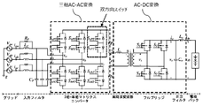
三相AC-DCコンバータの一実施態様について、図1に示す回路構成図を参照して説明する。図1に示す三相AC-DCコンバータは、三相交流電圧vinの各相に接続される1次側コンバータユニット(No.1~No.3)と、1次側コンバータユニットの出力側を1次側に接続するHFトランス(高周波トランス)と、HFトランスの2次側に接続され、整流ダイオードのブリッジ式の全波整流回路を用いて交流を直流に変換する2次側コンバータと、1次側コンバータユニットを制御する制御回路(図示せず)から構成される。制御回路は、各相に接続された1次側コンバータユニットに対して、120°位相差を設けてスイッチングする。 One embodiment of the three-phase AC-DC converter will be described with reference to the circuit configuration diagram shown in FIG. The three-phase AC-DC converter shown in FIG. an HF transformer (high-frequency transformer) connected to the primary side; a secondary-side converter connected to the secondary side of the HF transformer and converting AC to DC using a bridge-type full-wave rectifier circuit of rectifying diodes; It is composed of a control circuit (not shown) that controls the secondary converter unit. The control circuit performs switching with a 120° phase difference with respect to the primary converter units connected to each phase.
1次側コンバータユニットは、昇圧用リアクトルLbとブリッジレス整流用の第1および第2ダイオードD5,D6から成る昇圧ACチョッパ回路/PFCコンバータと、フルブリッジインバータ回路から構成される。
フルブリッジインバータ回路は、ハイサイドの第1スイッチS1とローサイドの第2スイッチS2が直列接続され、第1および第2スイッチに各々逆並列ダイオードD1,D2が接続された第1インバータレッグと、ハイサイドの第3スイッチS3とローサイドの第4スイッチS4が直列接続され、第3および第4スイッチに各々逆並列ダイオードD3,D4が接続された第2インバータレッグから構成され、第1インバータレッグと第2インバータレッグはフルブリッジ構成を形成している。スイッチQ1,Q2は基準相スイッチとなり、スイッチQ3,Q4は制御相スイッチとなり、それぞれアクティブスイッチとして動作する。
非平滑DCリンクキャパシタ(Cd)は、昇圧ACチョッパ回路の一部として作用すると同時に、フルブリッジ回路においては高周波周期での電圧源となる。低周波(商用周波)と高周波とを「リンク」する非平滑直流ステージとして位置付けられる要素である。
1次側コンバータユニットは、昇圧用リアクトルLbと、ブリッジレス整流用ダイオードD5,D6と、基準相スイッチQ1,Q2と、制御相スイッチQ4,Q4と、非平滑DCリンクキャパシタ(Cd)とから成り、昇圧形PFCコンバータを形成している。
The primary - side converter unit is composed of a boost AC chopper circuit/PFC converter composed of a boost reactor Lb and first and second bridgeless rectification diodes D5 and D6, and a full bridge inverter circuit.
The full-bridge inverter circuit is a first inverter in which a high-side first switch S1 and a low-side second switch S2 are connected in series, and antiparallel diodes D1 and D2 are connected to the first and second switches, respectively. and a second inverter leg in which a third high-side switch S3 and a fourth low-side switch S4 are connected in series, and anti-parallel diodes D3 and D4 are connected to the third and fourth switches, respectively. and the first inverter leg and the second inverter leg form a full bridge configuration. Switches Q 1 and Q 2 act as reference phase switches and switches Q 3 and Q 4 act as control phase switches, each operating as an active switch.
The non-smoothing DC link capacitor (C d ) acts as part of the boost AC chopper circuit and at the same time as the voltage source in the full bridge circuit at high frequency periods. It is an element positioned as a non-smooth DC stage that "links" low frequencies (commercial frequencies) and high frequencies.
The primary-side converter unit includes a boost reactor Lb , bridgeless rectifier diodes D5 and D6 , reference phase switches Q1 and Q2 , control phase switches Q4 and Q4 , and a non-smoothing DC link. and a capacitor (C d ) to form a boost PFC converter.
1次側コンバータユニットのフルブリッジインバータ回路は、各アクティブスイッチに並列に接続するロスレススナバキャパシタ(Cs1~Cs4)を利用して、部分共振のゼロ電圧ソフトスイッチング(ZVS)動作を行う。また、非平滑DCリンクキャパシタ(Cd)は、大容量アルミ電解コンデンサを使用しない、所謂、ケミコンレスであり、高いメンテナンス性と軽量・省スペース化を図ることができる。
図1に示す回路には、各相の交流電圧vin側にLCフィルタ(LfとCf)を設けているが、これは各相の交流電圧vinの高周波スイッチング成分を除去できることから、電源側における電磁ノイズの影響を軽減するためのものである。従って、LCフィルタを設けなくとも、三相AC-DCコンバータの機能を発揮することができる。
The full bridge inverter circuit of the primary side converter unit performs a partial resonance zero voltage soft switching (ZVS) operation using lossless snubber capacitors (C s1 to C s4 ) connected in parallel to each active switch. In addition, the non-smoothing DC link capacitor (C d ) does not use a large-capacity aluminum electrolytic capacitor, that is, it is a so-called chemicon-less capacitor, and high maintainability, light weight, and space saving can be achieved.
The circuit shown in FIG. 1 is provided with an LC filter (L f and C f ) on the AC voltage vin side of each phase. This is to reduce the influence of electromagnetic noise on the power supply side. Therefore, the function of a three-phase AC-DC converter can be exhibited without providing an LC filter.
1次側コンバータユニットのフルブリッジインバータ回路の4つのアクティブスイッチ(Q1~Q4)に対して、位相シフトPWM制御を用いることにより、電源電圧を検出することなく、高周波スイッチングを実現する。
図1に示す回路における位相シフトPWM制御は、図示しない位相シフトコントローラ(制御回路)により行う。図2に、制御機能ブロック図を付加した回路構成図を示す。図2に示すように、位相シフトコントローラは、U相、V相、W相にそれぞれ接続されたフルブリッジインバータ回路の4つのアクティブスイッチ(Q1~Q4)を、120°位相差を設けてスイッチングするように制御する。すなわち、図2の矢印Aの点線枠に示すように、2次側コンバータの出力直流電圧Voと出力電流Ioを、それぞれリファレンス電圧Vorefとリファレンス電流Iorefと比較することによりモニタリングし、Q1/Q2,Q4/Q3間の適切な位相シフト角φs
*に入力信号を変換する。そして、アクティブスイッチ(Q1~Q4)にゲート駆動回路ユニット(Gate Driver)がゲート駆動パルスを供給し、基準相アクティブスイッチQ1に対するQ4の導通開始区間、又は、同じく基準相アクティブスイッチQ2に対するQ3の導通開始区間を、相間で120°の位相差を設けて、各相ブリッジ回路の基準相レッグに応じて制御相レッグを遅らせる位相シフトパルス幅変調制御を行う。
By using phase shift PWM control for the four active switches (Q 1 to Q 4 ) of the full bridge inverter circuit of the primary side converter unit, high frequency switching is realized without detecting the power supply voltage.
Phase shift PWM control in the circuit shown in FIG. 1 is performed by a phase shift controller (control circuit) not shown. FIG. 2 shows a circuit configuration diagram to which a control function block diagram is added. As shown in FIG. 2, the phase shift controller has four active switches (Q 1 to Q 4 ) of a full-bridge inverter circuit connected to the U-phase, V-phase, and W-phase, respectively, with a 120° phase difference. Control to switch. That is, as shown in the dotted frame of arrow A in FIG. 2, the output DC voltage V o and the output current I o of the secondary converter are monitored by comparing them with the reference voltage V oref and the reference current I oref respectively, Convert the input signal to the appropriate phase shift angle φ s * between Q 1 /Q 2 and Q 4 /Q 3 . Then, a gate drive circuit unit (Gate Driver) supplies a gate drive pulse to the active switches (Q 1 to Q 4 ), and the conduction start interval of Q 4 with respect to the reference phase active switch Q 1 or the reference phase active switch Q 2 with a phase shift of 120° between the phases to provide phase shift pulse width modulation control that delays the control phase leg relative to the reference phase leg of each phase bridge circuit.
各相の交流電源(vin)は、昇圧用リアクトル(Lb)を介して、非平滑DCリンクキャパシタ(Cd)の端子電圧(vd)へ昇圧される。そのため、非平滑DCリンクキャパシタ(Cd)の端子電圧は、各相の交流電圧の半波整流に振幅変調をかけた包絡線を示す。
また同時に、非平滑DCリンクキャパシタ(Cd)は、位相シフトPWM制御により、フルブリッジ回路における高周波インバータ動作を行う。
The AC power supply (v in ) of each phase is stepped up to the terminal voltage (v d ) of the non-smoothing DC link capacitor (C d ) through the step-up reactor (L b ). Therefore, the terminal voltage of the non-smoothing DC link capacitor (C d ) shows an envelope obtained by applying amplitude modulation to the half-wave rectification of the AC voltage of each phase.
At the same time, the non-smoothing DC link capacitor (C d ) performs high frequency inverter operation in the full bridge circuit by phase shift PWM control.
ここで、回路の動作周波数(スイッチング周波数)fsを、1次側コンバータユニットのフルブリッジインバータ回路の直列共振周波数frより高く設定して、各アクティブスイッチ(Q1~Q4 )がZVSターンオフおよびゼロ電圧/ゼロ電流ソフトスイッチング(ZVZCS) ターンオンを実現する。回路の動作周波数fsは、一般的には、5~200kHz近傍で使用されているが、アクティブスイッチの高速化によりさらに、周波数が高くなる場合がある。 Here, the operating frequency (switching frequency) f s of the circuit is set higher than the series resonance frequency f r of the full bridge inverter circuit of the primary side converter unit, and each active switch (Q 1 to Q 4 ) is ZVS turned off. and zero voltage/zero current soft switching (ZVZCS) turn-on. The operating frequency fs of the circuit is generally used in the vicinity of 5 to 200 kHz, but the frequency may become higher as the speed of the active switch increases.
回路の制御方法は、基準相スイッチ(Q1,Q2)に対して、制御相スイッチ(Q3,Q4)のオンタイミングを調整する位相シフトPWM制御を適用する。このとき、回路動作の1 周期(Ts)における位相シフト期間をtφsと定義すると、tφsは下記数式で表される。ここで、φsは位相シフト角である。各相の交流電圧vinの正半サイクルと負半サイクルでアクティブスイッチのゲート信号の切り替えを行わなくとも、所望の動作を得られることから、各相の交流電圧vinの極性判別用センサが不要である。 The circuit control method applies phase shift PWM control for adjusting the ON timing of the control phase switches (Q 3 , Q 4 ) to the reference phase switches (Q 1 , Q 2 ). At this time, if the phase shift period in one cycle (T s ) of the circuit operation is defined as t φs , t φs is expressed by the following formula. where φ s is the phase shift angle. Since the desired operation can be obtained without switching the gate signal of the active switch in the positive half cycle and the negative half cycle of the AC voltage vin of each phase, the sensor for discriminating the polarity of the AC voltage vin of each phase is provided. No need.

次に、図1に示す回路構成の回路動作について説明する。
三相交流電源の各相の交流電圧vinが正の半サイクル(vs>0)において、本実施例の三相AC-DCコンバータの1次側コンバータユニットの動作は、以下に述べる12の動作モードから成る。本実施例の三相AC-DCコンバータの1次側コンバータユニットは、時間の経過に従い、アクティブスイッチをそれぞれのゲートトリガ信号によってオン/オフ制御することによって、t0~t11の区間において高周波電力変換を行う。
以下、t0~t11の各区間(tn~tn+1;n=0~5)における本実施例の三相AC-DCコンバータの1次側コンバータユニットの各動作モードについて説明する。
なお、参考までに、単相AC-DCコンバータにおける遷移モード図とモード動作波形図を、それぞれ図14と図15に示す。
Next, the circuit operation of the circuit configuration shown in FIG. 1 will be described.
The operation of the primary side converter unit of the three-phase AC-DC converter of this embodiment in the positive half cycle (v s >0) of the AC voltage v in of each phase of the three-phase AC power supply is as follows. It consists of operating modes. The primary-side converter unit of the three-phase AC-DC converter of this embodiment turns on/off the active switches according to the passage of time by respective gate trigger signals, so that high-frequency power is generated in the interval from t0 to t11 . do the conversion.
Each operation mode of the primary side converter unit of the three-phase AC-DC converter of the present embodiment in each section from t 0 to t 11 (t n to t n+1 ; n=0 to 5) will be described below.
For reference, a transition mode diagram and a mode operation waveform diagram in a single-phase AC-DC converter are shown in FIGS. 14 and 15, respectively.
<Mode 1:電力定常区間t0~t1>
アクティブスイッチ(Q1,Q4)がオン状態であり、各相の交流電流IinはVin-Lb-D5-S1-Vinの経路で流れ、昇圧用インダクタLbに磁気エネルギーが蓄積される。一方、高周波インバータでは、S1-T1-S4-Cd-S1の経路で電流が流れ、非平滑キャパシタCdから静電エネルギーが放出されてHFトランスへ電力供給される。
<Mode 1: Power steady section t 0 to t 1 >
The active switches (Q 1 , Q 4 ) are in the ON state, the AC current I in of each phase flows through the route of V in −L b −D 5 −S 1 −V in , and the magnetic energy is accumulated. On the other hand, in the high-frequency inverter, current flows through the path of S 1 -T 1 -S 4 -C d -S 1 , and electrostatic energy is released from the non-smoothing capacitor C d and supplied to the HF transformer.
<Mode 2:基準相レッグ部分共振区間t1~t2(ハイサイド->ローサイド)>
時刻t1において、スイッチS1のゲート信号を取り除くと、各相の交流電流IinはVin-Lb-D5-Cs1の経路を流れ、ハイサイドのアクティブスイッチQ1に並列のロスレススナバキャパシタCs1の充電を開始する。ロスレススナバキャパシタCs1の端子電圧、すなわちアクティブスイッチQ1の端子間電圧VQ1は、ゼロから緩やかに上昇を始める。これと同時に、ローサイドのアクティブスイッチQ2に並列のロスレススナバキャパシタCs2は放電を開始し、アクティブスイッチQ2の端子電圧VQ2は、非平滑DCリンクキャパシタCdの端子電圧vdより緩やかに下降を開始する。すなわち、ロスレススナバキャパシタCs1, Cs2およびHFトランスの漏れインダクタンスによる部分共振動作となる。
<Mode 2: Reference Phase Leg Partial Resonance Section t 1 to t 2 (High Side -> Low Side)>
At time t 1 , when the gate signal of switch S 1 is removed, alternating current I in of each phase flows through the path of V in -L b -D 5 -C s1 , resulting in a lossless current in parallel with high-side active switch Q 1 . Start charging the snubber capacitor Cs1 . The terminal voltage of the lossless snubber capacitor Cs1, that is, the voltage VQ1 between the terminals of the active switch Q1 starts to rise gently from zero. At the same time, the lossless snubber capacitor Cs2 in parallel with the low-side active switch Q2 begins to discharge, and the terminal voltage VQ2 of the active switch Q2 becomes slower than the terminal voltage vd of the non-smoothing DC link capacitor Cd . Start descending. In other words, the lossless snubber capacitors C s1 and C s2 and the leakage inductance of the HF transformer cause partial resonance operation.
<Mode 3:基準相レッグZVS区間t2~t3>
時刻t2において、ハイサイドのアクティブスイッチQ1の端子間電圧VQ1がvdまで達すると、アクティブスイッチQ1のZVSターンオフ動作が完了する。これと同時に、ローサイドのアクティブスイッチQ2の端子電圧VQ2がゼロまで下降すると、HFトランス1次側巻線電流ITが逆並列ダイオードD2へ転流し、S4-D2-T1-S4の経路で電流が流れる。この間にスイッチS2にゲート駆動パルスを供給して、ローサイドのアクティブスイッチQ2のゼロ電圧/ゼロ電流ソフトスイッチング(ZVZCS)ターンオンを実現する。一方、各相の入力交流電流Iinは、非平滑DCリンクキャパシタCdへ流れ込み、昇圧用インダクタLbの残存磁気エネルギーは、非平滑DCリンクキャパシタCdへの蓄積静電エネルギーとなる。
<Mode 3 : reference phase leg ZVS section t2 to t3>
At time t2, when the voltage VQ1 across the high-side active switch Q1 reaches vd , the ZVS turn - off operation of the active switch Q1 is completed. At the same time, when the terminal voltage V Q2 of the low-side active switch Q 2 drops to zero, the HF transformer primary winding current I T is commutated to the anti-parallel diode D 2 and S 4 −D 2 −T 1 − Current flows in the path of S4 . A gate drive pulse is applied to switch S2 during this time to achieve a zero voltage/zero current soft switching ( ZVZCS ) turn-on of the low side active switch Q2 . On the other hand, the input AC current Iin of each phase flows into the non-smoothing DC link capacitor Cd , and the residual magnetic energy of the boosting inductor Lb becomes electrostatic energy stored in the non-smoothing DC link capacitor Cd .
<Mode 4:制御相レッグ部分共振区間t3~t4(ローサイド->ハイサイド)>
時刻t3において、スイッチS4へのゲート駆動信号を取り除くと、HFトランス1次側巻線電流ITの一部は、ローサイドのアクティブスイッチQ4に並列のロスレススナバキャパシタCs4に電流が流れ込み、アクティブスイッチQ4の端子電圧VQ4はゼロから緩やかに上昇を始める。これと同時に、残りのHFトランスに流れる電流ITは、ハイサイドのアクティブスイッチQ3のロスレススナバキャパシタCs3を放電し、アクティブスイッチQ3の端子電圧VQ3は非平滑DCリンクキャパシタCdの端子電圧vdより緩やかに下降を始める。
<Mode 4: Control Phase Leg Partial Resonance Section t 3 to t 4 (Low Side -> High Side)>
At time t3 , removing the gate drive signal to switch S4 causes a portion of the HF transformer primary winding current IT to flow into lossless snubber capacitor Cs4 in parallel with low - side active switch Q4 . , the terminal voltage VQ4 of the active switch Q4 begins to slowly rise from zero. At the same time, the current I T flowing through the remaining HF transformer discharges the lossless snubber capacitor Cs3 of the high-side active switch Q3 , and the voltage VQ3 at the terminals of the active switch Q3 becomes the voltage of the non-smoothing DC link capacitor Cd . It begins to drop more slowly than the terminal voltage vd .
<Mode 5:制御相レッグZVS区間t4~t5>
時刻t4において、ローサイドのアクティブスイッチQ4の端子電圧VQ4がvdまで達すると、アクティブスイッチQ4のZVSターンオフ動作が完了する。これと同時に、ハイサイドのアクティブスイッチQ3の端子電圧VQ3がゼロまで下降すると、HFトランスに流れる電流ITは逆並列ダイオードD3へ転流し、D3-Cd-D2-T1-D3の経路で電流が流れる。この間にハイサイドのアクティブスイッチQ3のゲート駆動パルスを供給し、アクティブスイッチQ3のゼロ電圧/ゼロ電流ソフトスイッチング(ZVZCS)ターンオンを実現する。
<Mode 5 : Control phase leg ZVS section t4 to t5 >
At time t4, when the terminal voltage VQ4 of the low - side active switch Q4 reaches vd , the ZVS turn-off operation of the active switch Q4 is completed. At the same time, when the terminal voltage VQ3 of the high-side active switch Q3 drops to zero, the current I T flowing through the HF transformer is commutated to the anti - parallel diode D3, resulting in D3 - Cd-D2 - T1. A current flows through the path of -D3 . During this time a gate drive pulse for the high side active switch Q3 is provided to achieve a zero voltage/zero current soft switching ( ZVZCS ) turn on of the active switch Q3.
<Mode 6:電力供給定常区間t5~t6>
時刻t5において、逆並列ダイオードD3からスイッチS3へ転流し、HFトランスに流れる電流ITの極性が切り替わるとともに、各相の入力交流電流Iinの一部からHFトランスへ電力を供給する状態となる。
さらに、時刻t6において、逆並列ダイオードD2からスイッチS2への転流が完了すると、各相の入力交流電流Iinとともに非平滑DCリンクキャパシタCdも放電状態となりHFトランスに流れる電流ITとなる。
<Mode 6 : Power supply steady section t5 to t6 >
At time t5 , the polarity of the current IT flowing through the HF transformer is switched from the antiparallel diode D3 to the switch S3 , and power is supplied to the HF transformer from a portion of the input AC current Iin of each phase. state.
Furthermore, at time t6 , when the commutation from the anti - parallel diode D2 to the switch S2 is completed, the non - smoothing DC link capacitor Cd is discharged along with the input AC current Iin of each phase, and the current I flows through the HF transformer. becomes T.
<Mode 7:電力供給定常区間t6~t7>
時刻t6にて負荷電流が入力電流Iinを超えると、非平滑DCリンクキャパシタが放電モードとなり、第2スイッチQ2において逆並列ダイオードD2からスイッチS2へ転流する。
<Mode 7: Power supply steady section t 6 to t 7 >
When the load current exceeds the input current Iin at time t6, the non-smoothing DC link capacitor goes into discharge mode and commutates from antiparallel diode D2 to switch S2 in second switch Q2 .
<Mode 8:基準相レッグ部分共振区間t7~t8(ローサイド->ハイサイド)>
時刻t7において、スイッチS2のゲート駆動信号を取り除くと、HFトランス1次側巻線電流ITはローサイドのアクティブスイッチQ2に並列のロスレススナバキャパシタCs2の充電を開始する。ロスレススナバキャパシタCs2の端子電圧、すなわちアクティブスイッチQ2の端子間電圧VQ2は、ゼロから緩やかに上昇を始める。これと同時に、ハイサイドのアクティブスイッチQ1に並列のロスレススナバキャパシタCs1は放電を開始し、アクティブスイッチQ1の端子電圧VQ1は、非平滑DCリンクキャパシタCdの端子電圧vdより緩やかに下降を開始する。すなわち、ロスレススナバキャパシタCs1, Cs2およびHFトランスの漏れインダクタンスによる部分共振動作となる。
<Mode 8: Reference Phase Leg Partial Resonance Section t 7 to t 8 (Low Side -> High Side)>
At time t7 , removing the gate drive signal for switch S2 causes the HF transformer primary winding current IT to begin charging lossless snubber capacitor Cs2 in parallel with low-side active switch Q2 . The terminal voltage of the lossless snubber capacitor Cs2, that is, the voltage across the terminals of the active switch Q2 , VQ2 , begins to slowly rise from zero. At the same time, the lossless snubber capacitor Cs1 in parallel with the high-side active switch Q1 begins to discharge, and the voltage VQ1 across the active switch Q1 is slower than the voltage vd across the non-smoothing DC link capacitor Cd . start descending to In other words, the lossless snubber capacitors C s1 and C s2 and the leakage inductance of the HF transformer cause partial resonance operation.
<Mode 9:基準相レッグZVS区間t8~t9>
時刻t8において、ローサイドのアクティブスイッチQ2の端子間電圧VQ2がvdまで達すると、アクティブスイッチQ2のZVSターンオフ動作が完了する。これと同時に、ハイサイドのアクティブスイッチQ1の端子電圧VQ1がゼロまで下降すると、HFトランス1次側巻線電流ITが逆並列ダイオードD1へ転流し、S3-T1-D1-S3の経路で電流が流れる。この間にスイッチS1にゲート駆動パルスを供給して、ハイサイドのアクティブスイッチQ1のゼロ電圧/ゼロ電流ソフトスイッチング(ZVZCS)ターンオンを実現する。
<Mode 9 : reference phase leg ZVS section t8 to t9 >
At time t8, when the voltage VQ2 across the low - side active switch Q2 reaches vd , the ZVS turn-off operation of the active switch Q2 is completed. At the same time, when the terminal voltage V Q1 of the high-side active switch Q 1 drops to zero, the HF transformer primary winding current I T is commutated to the antiparallel diode D 1 and S 3 −T 1 −D 1 Current flows in the path of -S3 . A gate drive pulse is applied to switch S1 during this time to achieve a zero voltage/zero current soft switching (ZVZCS) turn-on of the high side active switch Q1 .
<Mode 10:制御相レッグ部分共振区間t9~t10(ハイサイド->ローサイド)>
時刻t9において、スイッチS3へのゲート駆動信号を取り除くと、HFトランス1次側巻線電流ITの一部は、ハイサイドのアクティブスイッチQ3に並列のロスレススナバキャパシタCs3に電流が流れ込み、アクティブスイッチQ3の端子電圧VQ3はゼロから緩やかに上昇を始める。これと同時に、残りのHFトランス1次側巻線電流ITは、ローサイドのアクティブスイッチQ4のロスレススナバキャパシタCs4を放電し、アクティブスイッチQ4の端子電圧VQ4は非平滑DCリンクキャパシタCdの端子電圧vdより緩やかに下降を始める。
<Mode 10: Control Phase Leg Partial Resonance Section t 9 to t 10 (High Side -> Low Side)>
At time t9 , removing the gate drive signal to switch S3 causes a portion of the HF transformer primary winding current IT to flow through lossless snubber capacitor Cs3 in parallel with high-side active switch Q3 . , and the terminal voltage VQ3 of active switch Q3 begins to slowly rise from zero. At the same time, the remaining HF transformer primary winding current IT discharges the lossless snubber capacitor Cs4 of the low-side active switch Q4, and the terminal voltage VQ4 of the active switch Q4 becomes the non -smoothing DC link capacitor C The terminal voltage v of d begins to fall more slowly than d .
<Mode 11:基準相レッグZVS区間t10~t11>
時刻t10において、ハイサイドのアクティブスイッチQ3の端子間電圧VQ3がvdまで達すると、アクティブスイッチQ3のZVSターンオフ動作が完了する。これと同時に、ローサイドのアクティブスイッチQ4の端子電圧VQ4がゼロまで下降すると、HFトランス1次側電流ITが逆並列ダイオードD4へ転流し、各相の入力交流電流Iinの一部と重なりながら、D4-T1-Vs-Lb-D5-Cd-D4の経路で電流が流れる。この間にスイッチS4にゲート駆動パルスを供給して、ローサイドのアクティブスイッチQ4のゼロ電圧/ゼロ電流ソフトスイッチング(ZVZCS)ターンオンを実現する。
<Mode 11 : reference phase leg ZVS interval t10 to t11 >
At time t10, when the voltage VQ3 across the high-side active switch Q3 reaches vd , the ZVS turn-off operation of the active switch Q3 is completed. At the same time, when the terminal voltage VQ4 of the low - side active switch Q4 drops to zero, the HF transformer primary current IT is commutated to the antiparallel diode D4, and a portion of the input AC current Iin of each phase is , a current flows along the route of D 4 -T 1 -V s -L b -D 5 -C d -D 4 . A gate drive pulse is applied to switch S4 during this time to achieve a zero voltage/zero current soft switching ( ZVZCS ) turn-on of the low side active switch Q4 .
<Mode 12:電力供給定常区間t11~t12>
時刻t11にて負荷電流が入力電流Iinより下回ると、基準相レッグのハイサイドスイッチQ1はD1からS1へ転流し、その順方向導通電流は次第に増加する。
<Mode 12: Power supply steady section t 11 to t 12 >
When the load current drops below the input current I in at time t 11 , the reference phase leg high-side switch Q 1 commutates from D 1 to S 1 and its forward conduction current gradually increases.
一方、各相の入力交流電圧vinが負の半サイクル(vs<0)においての動作モードは、アクティブスイッチ(Q1とQ2,Q3とQ4)、ブリッジレス整流用ダイオード(D5とD6),ロスレススナバキャパシタ(Cs1とCs2, Cs3とCs4)での転流現象がそれぞれ入れ替わり、各相の入力交流電圧vinが正の半サイクル(vs>0)と同様の動作モード遷移となる。 On the other hand, the operation mode in the negative half cycle (vs < 0 ) of the input AC voltage v in of each phase is active switches (Q 1 and Q 2 , Q 3 and Q 4 ), bridgeless rectifier diodes (D 5 and D 6 ), the commutation phenomena in the lossless snubber capacitors (C s1 and C s2 , C s3 and C s4 ) are switched, respectively, and the input AC voltage v in of each phase is a positive half cycle (v s >0). Operation mode transition is the same as
スイッチターンオフ時の電圧変化率(dv/dt)が最も高くなる非平滑DCリンクキャパシタCdの端子電圧vdのピーク付近においては、ターンオフ後にロスレススナバキャパシタの電荷が完全に放電する前に、相対するスイッチがオンすることになる。ここでは、この時の電圧を残留電圧とし、その際の不完全なZVS動作をセミZVS動作とする。 Near the peak of the terminal voltage vd of the non-smoothing DC link capacitor Cd, where the voltage change rate (dv/dt) at switch turn-off is the highest, before the charge of the lossless snubber capacitor is completely discharged after turn-off, relative switch is turned on. Here, the voltage at this time is defined as a residual voltage, and the imperfect ZVS operation at that time is defined as a semi-ZVS operation.
図1の三相AC-DCコンバータ回路のスイッチング周波数と出力直流電圧の関係について、図3及び図4を参照して説明する。図3,4は、実施例1の回路において、各相位相シフト角差とスイッチング周波数との関係を示したものである。各相において、高周波トランス(HFトランスT1,T2,T3)の巻き線間の漏れインダクタンスを用いて直列共振による電流反転を可能とする。本実施例の回路では、この直列共振周波数は20kHzに設定されている。なお、平滑キャパシタC7は100μF,負荷抵抗は20Ωである。
図3(1),(2)に、スイッチング周波数が30kHzで,各相位相シフト角差が120°と0°の場合におけるVo(出力直流電圧)及びVaco(出力交流電圧)を比較する。また、図3(3),(4)に、スイッチング周波数が26kHzで,各相位相シフト角差が120°と0°の場合におけるVo(出力直流電圧)及びVaco(出力交流電圧)を比較する。さらに、図4(1)(2)に、スイッチング周波数が22kHzで,各相位相シフト角差が120°と0°の場合におけるVo(出力直流電圧)及びVaco(出力交流電圧)を比較する。
The relationship between the switching frequency and the output DC voltage of the three-phase AC-DC converter circuit of FIG. 1 will be described with reference to FIGS. 3 and 4. FIG. 3 and 4 show the relationship between the phase shift angle difference of each phase and the switching frequency in the circuit of the first embodiment. In each phase, the leakage inductance between the windings of the high - frequency transformers (HF transformers T1, T2 , T3) is used to enable current reversal due to series resonance. In the circuit of this embodiment, this series resonance frequency is set to 20 kHz. The smoothing capacitor C7 is 100 μF and the load resistance is 20Ω.
3(1) and 3(2) compare Vo (output DC voltage) and Vaco (output AC voltage) when the switching frequency is 30 kHz and the phase shift angle difference of each phase is 120° and 0°. 3 (3) and (4) compare Vo (output DC voltage) and Vaco (output AC voltage) when the switching frequency is 26 kHz and the phase shift angle difference of each phase is 120° and 0°. . 4(1) and 4(2) compare Vo (output DC voltage) and Vaco (output AC voltage) when the switching frequency is 22 kHz and the phase shift angle difference of each phase is 120° and 0°.
図3,4のグラフの結果を図5の相関図に纏める。スイッチング周波数が直列共振周波数20kHzに近づくと、出力直流電圧が上がることがわかる。また、それと同時に波形のリプルが大きくなることがわかる。一方で、スイッチング周波数が同じ場合、各相位相シフト角差が0°よりも120°の方が、出力直流電圧が若干低下するが、波形のリプルが小さく、脈動が抑えられることがわかる。
図16~図18は、本実施例の三相AC-DCコンバータの出力並列方式の高周波周期における各相1次側波形、各相2次側波形および1次側スイッチング波形を示す。120°位相差による高周波電流生成とその出力合成およびゼロ電圧ソフトスイッチング動作が達成できていることがわかる。
The results of the graphs of FIGS. 3 and 4 are summarized in the correlation diagram of FIG. It can be seen that the output DC voltage rises when the switching frequency approaches the series resonance frequency of 20 kHz. At the same time, it can be seen that the ripple of the waveform increases. On the other hand, when the switching frequency is the same, the output DC voltage is slightly lower when the phase shift angle difference of each phase is 120° than when the phase shift angle is 0°, but the waveform ripple is small and pulsation is suppressed.
16 to 18 show primary side waveforms of each phase, secondary side waveforms of each phase, and primary side switching waveforms in the high frequency period of the output parallel system of the three-phase AC-DC converter of this embodiment. It can be seen that high-frequency current generation and its output synthesis with a 120° phase difference and zero-voltage soft switching operation can be achieved.
本実施例の三相AC-DCコンバータの回路構成図を図6に示す。上述の実施例1の回路構成(図1)では、三相交流電源側はΔ結線で接続されており、2次側のHFトランスの結線は並列接続されている。本実施例の三相AC-DCコンバータの回路構成では、実施例1の回路構成(図1)と異なり、三相交流電源側は、電源中性点と各相1線が共通結線とされるY結線で接続され、2次側のHFトランスの結線は直列接続されている。それ以外の構成は、実施例1の回路構成と同じであり、図6に示す三相AC-DCコンバータは、三相交流電圧vinの各相に接続される1次側コンバータユニット(No.1~No.3)と、1次側コンバータユニットの出力側を1次側に接続するHFトランス(高周波トランス)と、HFトランスの2次側に接続され、整流ダイオードのブリッジ式の全波整流回路を用いて交流を直流に変換する2次側コンバータと、1次側コンバータユニットを制御する制御回路(図示せず)から構成される。制御回路は、各相に接続された1次側コンバータユニットに対して、120°位相差を設けてスイッチングする。
1次側コンバータユニットは、昇圧用リアクトルLbとブリッジレス整流用の第1および第2ダイオードD5,D6から成る昇圧ACチョッパ回路/PFCコンバータと、フルブリッジインバータ回路から構成される。
FIG. 6 shows a circuit configuration diagram of the three-phase AC-DC converter of this embodiment. In the circuit configuration of the first embodiment described above (FIG. 1), the three-phase AC power supply side is connected by Δ connection, and the connection of the HF transformer on the secondary side is connected in parallel. In the circuit configuration of the three-phase AC-DC converter of this embodiment, unlike the circuit configuration of Embodiment 1 (Fig. 1), on the three-phase AC power supply side, the neutral point of the power supply and one line for each phase are connected in common. They are connected by Y connection, and the connection of the HF transformer on the secondary side is connected in series. The rest of the configuration is the same as the circuit configuration of the first embodiment, and the three-phase AC-DC converter shown in FIG. 6 is a primary-side converter unit (No. 1 to No. 3), an HF transformer (high-frequency transformer) that connects the output side of the primary-side converter unit to the primary side, and a bridge-type full-wave rectifier of rectifying diodes that is connected to the secondary side of the HF transformer. It consists of a secondary converter that converts alternating current to direct current using a circuit, and a control circuit (not shown) that controls the primary converter unit. The control circuit performs switching with a 120° phase difference with respect to the primary converter units connected to each phase.
The primary - side converter unit is composed of a boost AC chopper circuit/PFC converter composed of a boost reactor Lb and first and second bridgeless rectification diodes D5 and D6, and a full bridge inverter circuit.
図7,8にスイッチング周波数と出力直流電圧のグラフ及び相関図を示す。図7(1),(2)及び図8に示すように、スイッチング周波数が直列共振周波数20kHzに近い22kHzの場合、実施例1と同様に、各相位相シフト角差が0°よりも120°の方が、出力直流電圧が若干低下するが、波形のリプルが小さく、脈動が抑えられることがわかる。
また、図7(2)のリプルの拡大した図7(3)から、出力電圧が入力電圧(60Hz)の6倍のリプル(360Hz)を有することが確認できた。なお、各相位相シフト角差120°の場合は、出力電圧の曲線が安定状態に達する時間が、各相位相シフト角差0°の場合よりも長いことも確認されている。
7 and 8 show graphs and correlation diagrams of switching frequency and output DC voltage. As shown in FIGS. 7(1), 7(2) and 8, when the switching frequency is 22 kHz, which is close to the series resonance frequency of 20 kHz, the phase shift angle difference of each phase is 120° rather than 0° as in the first embodiment. It can be seen that although the output DC voltage is slightly lower in the case of , the ripple in the waveform is smaller and the pulsation is suppressed.
Also, from FIG. 7(3), which is an enlarged view of the ripple in FIG. 7(2), it was confirmed that the output voltage has a ripple (360 Hz) six times as large as the input voltage (60 Hz). It is also confirmed that the output voltage curve reaches a stable state at a phase shift angle difference of 120° for each phase longer than when the phase shift angle difference for each phase is 0°.
本実施例の三相AC-DCコンバータの回路構成図を図9に示す。上述の実施例1の回路構成(図1)では、三相交流電源側はΔ結線で接続されており、2次側のHFトランスの結線は並列接続されているが、本実施例の三相AC-DCコンバータの回路構成では、図9に示すように、三相交流電源側はΔ結線で接続され、2次側のHFトランスの結線は直列接続されている。それ以外の構成は、実施例1の回路構成と同じである。
高周波トランスの2次側を直列結線にすることにより、各相あたりの入力直列接続が実現でき、大型電動機駆動など産業用高電圧ドライブシステムに適用できる。
図19~図21は、本実施例の三相AC-DCコンバータの出力直列方式の高周波周期における各相1次側波形、各相2次側波形および1次側スイッチング波形を示す。120°位相差による高周波電流生成とその出力合成およびゼロ電圧ソフトスイッチング動作が達成できていることがわかる。
FIG. 9 shows a circuit diagram of the three-phase AC-DC converter of this embodiment. In the circuit configuration of the first embodiment described above (FIG. 1), the three-phase AC power supply side is connected by Δ connection, and the connection of the HF transformer on the secondary side is connected in parallel. In the circuit configuration of the AC-DC converter, as shown in FIG. 9, the side of the three-phase AC power supply is connected by delta connection, and the connection of the HF transformer on the secondary side is connected in series. Other configurations are the same as the circuit configuration of the first embodiment.
By connecting the secondary side of the high-frequency transformer in series, it is possible to realize serial connection of inputs for each phase, and it can be applied to industrial high-voltage drive systems such as those for driving large electric motors.
19 to 21 show primary side waveforms of each phase, secondary side waveforms of each phase, and primary side switching waveforms in a high frequency period of the output series system of the three-phase AC-DC converter of this embodiment. It can be seen that high-frequency current generation and its output synthesis with a 120° phase difference and zero-voltage soft switching operation can be achieved.
本実施例の三相AC-DCコンバータの回路構成図を図10に示す。上述の実施例2の回路構成(図6)では、三相交流電源側は、電源中性点と各相1線が共通結線とされるY結線で接続され、2次側のHFトランスの結線は直列接続されているが、本実施例の三相AC-DCコンバータの回路構成では、図10に示すように、三相交流電源側は、電源中性点と各相1線が共通結線とされるY結線で接続され、2次側のHFトランスの結線は並列接続されている。それ以外の構成は、実施例2の回路構成と同じである。
高周波トランスの2次側を並列結線にすることにより、交流電源周波数の2倍周波数の電力脈動を軽減でき、これにより、出力平滑フィルタ容量を低減可能にできる。なお、従来の三相整流コンバータ同様に、6倍周波数生成分は現われるが、その電力脈動が小さく、出力フィルタで容易に除去することができる。
実施例1~4の如く、本発明の三相AC-DCコンバータにおける高周波トランスの2次側は、用途に応じて並列結線(低インピーダンス負荷の場合)または直列結線(高インピーダンス負荷の場合)を用途に応じて選択できる。
FIG. 10 shows a circuit diagram of the three-phase AC-DC converter of this embodiment. In the circuit configuration of
By connecting the secondary side of the high-frequency transformer in parallel, it is possible to reduce the power pulsation of the double frequency of the AC power supply frequency, thereby making it possible to reduce the output smoothing filter capacity. As in the conventional three-phase rectifying converter, the 6-fold frequency component appears, but its power ripple is small and can be easily removed by an output filter.
As in Examples 1 to 4, the secondary side of the high-frequency transformer in the three-phase AC-DC converter of the present invention is connected in parallel (for low impedance loads) or in series (for high impedance loads) depending on the application. It can be selected according to the application.
本実施例の三相AC-DCコンバータの回路構成図を図11に示す。本実施例の三相AC-DCコンバータは、比較的大容量電源に対して有効となる回路構成である。本実施例の回路構成では、三相交流電源側はΔ結線で接続されており、2次側のHFトランスの結線は並列接続されているが、実施例1の回路構成(図1)と異なり、図11に示すように、各相に昇圧ACチョッパ回路及びフルブリッジインバータ回路から成る低周波交流から高周波交流に変換する1次側コンバータユニットが3ユニット直列接続されている。1次側コンバータユニットNo.1~No.9の構成とその他の構成は実施例1の回路構成と同じである。
同一相に直列接続されたそれぞれの1次側コンバータユニット(No.1~No.3,No4~No.6,No.7~No.9)内部では、位相シフトコントローラ(図示せず)により、それぞれのフルブリッジインバータ回路の4つのアクティブスイッチ(Q1~Q4)を、出力指令に応じて位相差を設けてスイッチングする位相シフトパルス幅変調を適用する。さらに、U相、V相、W相にそれぞれ接続されたフルブリッジインバータ回路(No.1とNo.4とNo.7,No.2とNo.5とNo.8,No.3とNo.6とNo.9)のそれぞれの4つのアクティブスイッチ(Q1~Q4)は120°位相差を設けてスイッチングするように位相シフトコントローラにより制御される。
本実施例の三相AC-DCコンバータでは、1次側コンバータユニットは、各相の最小ユニットに対して位相シフトパルス幅変調を適用し、各相における直列接続された最小ユニット同士が360°/Nの位相差を設けられ(ここで、Nは同一相に直列接続されたユニット数であり、本実施例ではN=3になる)、相間は120°の位相差を設けられる。
FIG. 11 shows a circuit diagram of the three-phase AC-DC converter of this embodiment. The three-phase AC-DC converter of this embodiment has a circuit configuration that is effective for a relatively large-capacity power supply. In the circuit configuration of this embodiment, the three-phase AC power supply side is connected by Δ connection, and the connection of the HF transformer on the secondary side is connected in parallel. , and as shown in FIG. 11, three primary side converter units for converting low-frequency alternating current to high-frequency alternating current are connected in series, each comprising a step-up AC chopper circuit and a full-bridge inverter circuit for each phase. The configuration of the primary side converter units No. 1 to No. 9 and other configurations are the same as the circuit configuration of the first embodiment.
Inside each primary side converter unit (No.1 to No.3, No.4 to No.6, No.7 to No.9) connected in series in the same phase, a phase shift controller (not shown) Phase shift pulse width modulation is applied to switch the four active switches (Q 1 to Q 4 ) of each full bridge inverter circuit with a phase difference according to the output command. Furthermore, full-bridge inverter circuits (No.1, No.4 and No.7, No.2, No.5 and No.8, No.3 and No.8, No.3 and No.8, No.3 and No.8, No.3 and No.7, No.2 and No.5 and No.8, No.3 and No.7, No.2 and No.5 and No.8, No.3 and No.8, No.3 and No.8, No.4 and No.7, No.2 and No.5 and No.8, No.3 and No.8, 6 and No. 9 ) are controlled by a phase shift controller to switch with a 120 ° phase difference.
In the three-phase AC-DC converter of this embodiment, the primary side converter unit applies phase shift pulse width modulation to the minimum unit of each phase, and the minimum units connected in series in each phase are 360°/ A phase difference of N is provided (here, N is the number of units connected in series in the same phase, and N=3 in this embodiment), and a phase difference of 120° is provided between the phases.
図12と図13は、上述の実施例1~4における三相AC-DCコンバータにおいて、それぞれ2次側HFトランスの結線が直列接続と並列接続の場合の2次側コンバータにおける三相交流電源側の力率改善(PFC)動作を示すシミュレーション波形を示している。図12と図13から、2次側HFトランスの結線が直列接続と並列接続の双方とも、各相(U相、V相、W相)の力率1運転を実現しており、PFC動作が可能であることが確認できる。 12 and 13 show the three-phase AC power supply side in the secondary converter when the secondary side HF transformer is connected in series and in parallel, respectively, in the three-phase AC-DC converters in Examples 1 to 4 described above. 2 shows simulated waveforms illustrating power factor correction (PFC) operation of the . From FIGS. 12 and 13, both the series connection and the parallel connection of the secondary side HF transformer realize a power factor operation of 1 for each phase (U phase, V phase, W phase), and the PFC operation is It can be confirmed that it is possible.
本発明の三相AC-DCコンバータは、直流給電が有効に利用できる分野、例えばスマートグリッドなどの電力分野、発電プラントや製造所など産業分野ならびに船舶・鉄道などの輸送分野におけるAC-DCコンバータとして有用である。また、電池を動力源とする自動車や船舶(フェリー旅客船)などへの非接触給電にも適用可能である。 The three-phase AC-DC converter of the present invention can be used as an AC-DC converter in fields where DC power supply can be effectively used, such as power fields such as smart grids, industrial fields such as power generation plants and manufacturing plants, and transportation fields such as ships and railways. Useful. It can also be applied to non-contact power supply to automobiles, ships (passenger ferries), etc. that use batteries as power sources.
vin 三相交流電圧
vout 出力直流電圧
Q1~Q4 アクティブスイッチ
S1~S4 トランジスタスイッチ
D1~D4 逆並列ダイオード
D5,D6 逆流阻止/整流ダイオード
Cd 非平滑DCリンクキャパシタ
Lb 昇圧用リアクトル
CS1~CS4 ZVS用ロスレススナバキャパシタ
v in three-phase AC voltage v out output DC voltage Q 1 to Q 4 active switches S 1 to S 4 transistor switches D 1 to D 4 antiparallel diodes D 5 , D 6 reverse blocking/rectifying diodes C d non-smoothing DC link capacitor L b boosting reactor C S1 to C S4 Lossless snubber capacitor for ZVS
Claims (16)
前記フルブリッジインバータ回路の出力側を1次側に接続する高周波トランスと、
前記高周波トランスの2次側に接続され、全波整流回路を有し交流を直流に変換する2次側コンバータと、
前記フルブリッジインバータ回路を構成する半導体スイッチを制御する制御回路、
を備え、
各相に接続された前記フルブリッジインバータ回路は、120°位相差を設けてスイッチングされることを特徴とする三相AC-DCコンバータ。 A primary side converter composed of a boost AC chopper circuit (power factor correction converter) and a full bridge inverter circuit connected to each phase of a three-phase AC power supply;
a high-frequency transformer that connects the output side of the full-bridge inverter circuit to the primary side;
a secondary-side converter connected to the secondary side of the high-frequency transformer and having a full-wave rectifier circuit for converting alternating current to direct current;
a control circuit for controlling semiconductor switches that constitute the full-bridge inverter circuit;
with
A three-phase AC-DC converter, wherein the full-bridge inverter circuits connected to each phase are switched with a phase difference of 120°.
ハイサイドの第1スイッチとローサイドの第2スイッチが直列接続され、第1および第2スイッチに各々逆並列ダイオードが接続された第1インバータレッグと、
ハイサイドの第3スイッチとローサイドの第4スイッチが直列接続され、第3および第4スイッチに各々逆並列ダイオードが接続された第2インバータレッグと、
インバータレッグに並列に設けられた非平滑DCリンクキャパシタと、
各相の交流電源の一端に直列接続された昇圧用リアクトルと、
インバータレッグと入力用交流電源の間に接続されるブリッジレス整流用の第1および第2ダイオードと、
を備え、
第1インバータレッグと第2インバータレッグとがフルブリッジ構成を成す請求項1~7の何れかの三相AC-DCコンバータ。 The primary side converter,
a first inverter leg having a first high-side switch and a second low-side switch connected in series, with an antiparallel diode connected to each of the first and second switches;
a second inverter leg having a third high-side switch and a fourth low-side switch connected in series, with an antiparallel diode connected to each of the third and fourth switches;
a non-smoothing DC link capacitor in parallel with the inverter leg;
a step-up reactor connected in series to one end of each phase AC power supply;
first and second diodes for bridgeless rectification connected between the inverter leg and the input AC power supply;
with
A three-phase AC-DC converter according to any preceding claim, wherein the first inverter leg and the second inverter leg form a full bridge configuration.
各相の交流電源の一端に直列接続された前記昇圧用リアクトルの端から分岐して、一方はブリッジレス整流用の第1ダイオードを介して第1インバータレッグの第1スイッチ側と接続され、他方はブリッジレス整流用の第2ダイオードを介して第1インバータレッグの第2スイッチ側と接続される請求項8~11の何れかの三相AC-DCコンバータ。 each phase AC power source is connected to the high side of said inverter leg;
Branched from the end of the step-up reactor connected in series to one end of the AC power supply of each phase, one side is connected to the first switch side of the first inverter leg via the first diode for bridgeless rectification, and the other side is connected to the first switch side of the first inverter leg. is connected with the second switch side of the first inverter leg through a second diode for bridgeless rectification.
各相に接続された前記フルブリッジインバータ回路の半導体スイッチが120°位相差を設けてスイッチングされ、
第1スイッチに対する第4スイッチの導通開始区間、或は、第2スイッチに対する第3スイッチの導通開始区間を、各相ブリッジ回路の基準相レッグに応じて制御相レッグを遅らせる位相シフトパルス幅変調制御を行うことを特徴とする三相AC-DCコンバータ制御方法。 A control method for a three-phase AC-DC converter according to any one of claims 8 to 14 ,
The semiconductor switches of the full bridge inverter circuit connected to each phase are switched with a 120° phase difference,
Phase shift pulse width modulation control for delaying the conduction start interval of the fourth switch with respect to the first switch or the conduction start interval of the third switch with respect to the second switch in accordance with the reference phase leg of each phase bridge circuit. A three-phase AC-DC converter control method characterized by performing
前記三相交流電源がΔ結線であり、各相の前記1次側コンバータが各相の交流電源の両端に接続され、
同一相に接続される各コンバータユニットは2π/Nの位相差を設けてスイッチングされる請求項15の三相AC-DCコンバータ制御方法。 The primary-side converter includes N (N≧2) units connected in series and each phase is connected to a converter unit that converts a low-frequency alternating current to a high-frequency alternating current, and is composed of a boost AC chopper circuit and a full-bridge inverter circuit;
The three-phase AC power supply is a Δ connection, and the primary converter of each phase is connected to both ends of the AC power supply of each phase,
16. The three-phase AC-DC converter control method according to claim 15 , wherein each converter unit connected in the same phase is switched with a phase difference of 2π/N.
Priority Applications (1)
| Application Number | Priority Date | Filing Date | Title |
|---|---|---|---|
| JP2018053681A JP7121971B2 (en) | 2018-03-21 | 2018-03-21 | Three-phase AC-DC converter |
Applications Claiming Priority (1)
| Application Number | Priority Date | Filing Date | Title |
|---|---|---|---|
| JP2018053681A JP7121971B2 (en) | 2018-03-21 | 2018-03-21 | Three-phase AC-DC converter |
Publications (2)
| Publication Number | Publication Date |
|---|---|
| JP2019169991A JP2019169991A (en) | 2019-10-03 |
| JP7121971B2 true JP7121971B2 (en) | 2022-08-19 |
Family
ID=68107639
Family Applications (1)
| Application Number | Title | Priority Date | Filing Date |
|---|---|---|---|
| JP2018053681A Active JP7121971B2 (en) | 2018-03-21 | 2018-03-21 | Three-phase AC-DC converter |
Country Status (1)
| Country | Link |
|---|---|
| JP (1) | JP7121971B2 (en) |
Families Citing this family (3)
| Publication number | Priority date | Publication date | Assignee | Title |
|---|---|---|---|---|
| EP4280443A4 (en) * | 2021-01-21 | 2024-03-13 | Huawei Digital Power Tech Co Ltd | Resonant ac/dc converter, electronic device, and adapter |
| CN114157158A (en) * | 2021-12-02 | 2022-03-08 | 襄阳九鼎昊天环保设备有限公司 | Multi-group composite high-frequency high-voltage electrostatic power supply |
| CN115189587B (en) * | 2022-09-07 | 2022-12-13 | 深圳市恒运昌真空技术有限公司 | Three-phase resonant rectifier and control method thereof |
Citations (4)
| Publication number | Priority date | Publication date | Assignee | Title |
|---|---|---|---|---|
| JP2013516953A (en) | 2010-01-11 | 2013-05-13 | コーニンクレッカ フィリップス エレクトロニクス エヌ ヴィ | AC / DC conversion circuit |
| JP2015228316A (en) | 2014-05-30 | 2015-12-17 | 国立大学法人神戸大学 | Commercial frequency-high frequency converter for induction heating, and method of controlling the same |
| WO2016024223A1 (en) | 2014-08-13 | 2016-02-18 | Inesc Porto- Instituto De Engenharia De Sistemas E Computadores Do Porto | Ac/dc converter with three to single phase matrix converter, full-bridge ac/dc converter and hf transformer |
| JP2017199628A (en) | 2016-04-28 | 2017-11-02 | 国立大学法人神戸大学 | Single state commercial frequency-high frequency converter for induction heating and control method for the same |
Family Cites Families (2)
| Publication number | Priority date | Publication date | Assignee | Title |
|---|---|---|---|---|
| EP0562662B1 (en) * | 1992-03-27 | 1997-05-21 | Ascom FRAKO GmbH | AC/DC converter |
| US9729066B1 (en) * | 2016-06-30 | 2017-08-08 | Hella Kgaa Hueck & Co. | Electric power conversion apparatus having single-phase and multi-phase operation modes |
-
2018
- 2018-03-21 JP JP2018053681A patent/JP7121971B2/en active Active
Patent Citations (4)
| Publication number | Priority date | Publication date | Assignee | Title |
|---|---|---|---|---|
| JP2013516953A (en) | 2010-01-11 | 2013-05-13 | コーニンクレッカ フィリップス エレクトロニクス エヌ ヴィ | AC / DC conversion circuit |
| JP2015228316A (en) | 2014-05-30 | 2015-12-17 | 国立大学法人神戸大学 | Commercial frequency-high frequency converter for induction heating, and method of controlling the same |
| WO2016024223A1 (en) | 2014-08-13 | 2016-02-18 | Inesc Porto- Instituto De Engenharia De Sistemas E Computadores Do Porto | Ac/dc converter with three to single phase matrix converter, full-bridge ac/dc converter and hf transformer |
| JP2017199628A (en) | 2016-04-28 | 2017-11-02 | 国立大学法人神戸大学 | Single state commercial frequency-high frequency converter for induction heating and control method for the same |
Also Published As
| Publication number | Publication date |
|---|---|
| JP2019169991A (en) | 2019-10-03 |
Similar Documents
| Publication | Publication Date | Title |
|---|---|---|
| US8295069B2 (en) | Power conversion with added pseudo-phase | |
| US8300426B2 (en) | Converter for enhanced efficiency power conversion | |
| US8514601B2 (en) | Power conversion with added pseudo-phase | |
| US20100259955A1 (en) | Soft switching power converter | |
| CA2768517A1 (en) | Dc-dc converter circuit for high input-to-output voltage conversion | |
| JP2003324956A (en) | Method of controlling series resonant bridge inverter circuit and the circuit | |
| Amirabadi | A new class of high-power-density universal power converters | |
| JP7121971B2 (en) | Three-phase AC-DC converter | |
| Chen et al. | Analysis and design considerations of an improved ZVS full-bridge DC-DC converter | |
| JP2017199628A (en) | Single state commercial frequency-high frequency converter for induction heating and control method for the same | |
| JP3681596B2 (en) | DC power supply | |
| US10848071B2 (en) | Highly reliable and compact universal power converter | |
| JP2001224172A (en) | Power converter | |
| JP4488130B2 (en) | Power converter | |
| Mozaffari et al. | A multifunction series inductive AC-link universal power converter with reduced-switch count | |
| KR20100006785A (en) | Three phase current-fed dc/dc converter with active clamp | |
| WO2013035671A1 (en) | Power conversion device, control method, and program | |
| Kumar et al. | A Two Stage Buck–Boost Converter with Soft Switching for Wind Power Applications | |
| Khodabandeh et al. | Capacitive-Link Universal Converters with Low Voltage Stress and High Switching Frequency | |
| Li et al. | A current fed two-inductor boost converter for grid interactive photovoltaic applications | |
| SARASWATHI et al. | Modeling and Simulation of BLDC Motor Drive Fed by Isolated DC-DC Converter | |
| Lin et al. | DC converter with full-bridge converters and flying capacitors | |
| MX2012009617A (en) | Dc-dc converter circuit for high input-to-output voltage conversion. |
Legal Events
| Date | Code | Title | Description |
|---|---|---|---|
| A621 | Written request for application examination |
Free format text: JAPANESE INTERMEDIATE CODE: A621 Effective date: 20210317 |
|
| A131 | Notification of reasons for refusal |
Free format text: JAPANESE INTERMEDIATE CODE: A131 Effective date: 20220308 |
|
| A521 | Request for written amendment filed |
Free format text: JAPANESE INTERMEDIATE CODE: A523 Effective date: 20220506 |
|
| TRDD | Decision of grant or rejection written | ||
| A01 | Written decision to grant a patent or to grant a registration (utility model) |
Free format text: JAPANESE INTERMEDIATE CODE: A01 Effective date: 20220727 |
|
| A61 | First payment of annual fees (during grant procedure) |
Free format text: JAPANESE INTERMEDIATE CODE: A61 Effective date: 20220801 |
|
| R150 | Certificate of patent or registration of utility model |
Ref document number: 7121971 Country of ref document: JP Free format text: JAPANESE INTERMEDIATE CODE: R150 |