JP7085453B2 - Diagnostic method for power converters and power converters - Google Patents
Diagnostic method for power converters and power converters Download PDFInfo
- Publication number
- JP7085453B2 JP7085453B2 JP2018196372A JP2018196372A JP7085453B2 JP 7085453 B2 JP7085453 B2 JP 7085453B2 JP 2018196372 A JP2018196372 A JP 2018196372A JP 2018196372 A JP2018196372 A JP 2018196372A JP 7085453 B2 JP7085453 B2 JP 7085453B2
- Authority
- JP
- Japan
- Prior art keywords
- voltage
- current
- conversion device
- power conversion
- switching element
- Prior art date
- Legal status (The legal status is an assumption and is not a legal conclusion. Google has not performed a legal analysis and makes no representation as to the accuracy of the status listed.)
- Active
Links
Images


Classifications
-
- H—ELECTRICITY
- H02—GENERATION; CONVERSION OR DISTRIBUTION OF ELECTRIC POWER
- H02M—APPARATUS FOR CONVERSION BETWEEN AC AND AC, BETWEEN AC AND DC, OR BETWEEN DC AND DC, AND FOR USE WITH MAINS OR SIMILAR POWER SUPPLY SYSTEMS; CONVERSION OF DC OR AC INPUT POWER INTO SURGE OUTPUT POWER; CONTROL OR REGULATION THEREOF
- H02M7/00—Conversion of ac power input into dc power output; Conversion of dc power input into ac power output
- H02M7/42—Conversion of dc power input into ac power output without possibility of reversal
- H02M7/44—Conversion of dc power input into ac power output without possibility of reversal by static converters
- H02M7/48—Conversion of dc power input into ac power output without possibility of reversal by static converters using discharge tubes with control electrode or semiconductor devices with control electrode
- H02M7/53—Conversion of dc power input into ac power output without possibility of reversal by static converters using discharge tubes with control electrode or semiconductor devices with control electrode using devices of a triode or transistor type requiring continuous application of a control signal
- H02M7/537—Conversion of dc power input into ac power output without possibility of reversal by static converters using discharge tubes with control electrode or semiconductor devices with control electrode using devices of a triode or transistor type requiring continuous application of a control signal using semiconductor devices only, e.g. single switched pulse inverters
- H02M7/5387—Conversion of dc power input into ac power output without possibility of reversal by static converters using discharge tubes with control electrode or semiconductor devices with control electrode using devices of a triode or transistor type requiring continuous application of a control signal using semiconductor devices only, e.g. single switched pulse inverters in a bridge configuration
-
- G—PHYSICS
- G01—MEASURING; TESTING
- G01R—MEASURING ELECTRIC VARIABLES; MEASURING MAGNETIC VARIABLES
- G01R31/00—Arrangements for testing electric properties; Arrangements for locating electric faults; Arrangements for electrical testing characterised by what is being tested not provided for elsewhere
- G01R31/40—Testing power supplies
- G01R31/42—AC power supplies
Description
本発明は、異常診断機能を備えた電力変換装置及び電力変換装置の診断方法に関し、特に、大容量の電力変換装置の異常診断に好適である。 The present invention relates to a power conversion device having an abnormality diagnosis function and a method for diagnosing the power conversion device, and is particularly suitable for abnormality diagnosis of a large-capacity power conversion device.
鉄道や大型産業機器向けの電動機を制御するために用いる電力変換装置や、電力系統用などの大容量の周波数変換に用いる電力変換装置は、大容量の電力用半導体素子を用いて、高電圧かつ大電流の電力制御を行うものである。 Power converters used to control electric power for railways and large industrial equipment, and power converters used for large-capacity frequency conversion such as for power systems, use large-capacity semiconductor elements for electric power to achieve high voltage. It controls the power of a large current.
このような機器では、稼働中に故障が発生すると、システムの損傷や計画外のシステム停止が生じ、大きな経済的損失が発生する可能性がある。こうした状況を防止する目的で、電力変換装置の劣化や異常を検出し、機能停止による破壊防止、機器を更新する必要性の関係者への通知、また電力変換装置の延命制御等が必要である。 Failures of such equipment during operation can result in system damage and unplanned system outages, which can result in significant economic loss. For the purpose of preventing such a situation, it is necessary to detect deterioration or abnormality of the power conversion device, prevent destruction due to outage, notify related parties of the need to update the device, and control the life extension of the power conversion device. ..
電力変換装置の故障要因として、半導体スイッチング素子の過熱が知られている。半導体スイッチング素子は、その接合温度(Tj)が定格以上に高い状態で動作させると破壊に到る。このため、電力変換装置には放熱設計が施されている。 Overheating of semiconductor switching elements is known as a cause of failure of power conversion devices. A semiconductor switching element will be destroyed if it is operated in a state where its junction temperature (Tj) is higher than the rating. Therefore, the power conversion device is designed to dissipate heat.
ここで、半導体素子は、実装のために半導体チップと熱膨張係数の異なる材料が積層されていることから、稼働中の半導体チップの自己発熱による熱応力の蓄積により、はんだやボンドワイヤが経年劣化することを避けられない。
よって、半導体スイッチング素子の熱インピーダンスは継時的に上昇し、半導体素子が過熱することがある。
Here, since the semiconductor element is laminated with a material having a coefficient of thermal expansion different from that of the semiconductor chip for mounting, the solder and the bond wire deteriorate over time due to the accumulation of thermal stress due to the self-heating of the semiconductor chip in operation. It is inevitable to do.
Therefore, the thermal impedance of the semiconductor switching element may increase over time, and the semiconductor element may overheat.
一方で、電力変換装置は無保守が前提であるため、通常の保全作業では半導体スイッチング素子そのものを点検することは極めて少なく、使用開始から一定期間が経過したタイミングで機器自体の更新を行う。 On the other hand, since the power conversion device is premised on no maintenance, it is extremely rare to inspect the semiconductor switching element itself in normal maintenance work, and the device itself is updated when a certain period of time has passed from the start of use.
しかしながら、電力変換装置は、その使用環境によっては劣化の進行が加速され、電力変換装置の寿命はそれぞれに異なる。そのため、それぞれの電力変換装置の状態をオンラインで監視し、機器更新のタイミングを個別に最適化することによる保守コストの低減が望まれている。 However, the progress of deterioration of the power conversion device is accelerated depending on the usage environment, and the life of the power conversion device is different for each. Therefore, it is desired to reduce the maintenance cost by monitoring the status of each power conversion device online and optimizing the timing of device update individually.
その中で、簡便な方法で電力変換装置を状態監視する技術として、システム稼働中に接合温度を測定する技術が知られている。
半導体スイッチング素子の内部に温度センサを内蔵する方法があるが、センサを集積させることにコストがかかり、また温度センサの応答速度や信頼性の観点で課題が多い。
Among them, as a technique for monitoring the state of the power conversion device by a simple method, a technique for measuring the junction temperature during system operation is known.
There is a method of incorporating a temperature sensor inside the semiconductor switching element, but it is costly to integrate the sensor, and there are many problems in terms of the response speed and reliability of the temperature sensor.
また、半導体スイッチング素子の電気特性の温度依存性を利用して、接合温度を推定する技術が知られている。例えば、特許文献1には、IGBT(Insulated Gate Bipolar Transistor)素子のスイッチオフ段階のゲート-エミッタ電圧特性において、ミラープラトーの開始段階から終了段階までの遅延時間を検出することで、IGBT素子の接合温度を決定し、平均接合温度の持続的な上昇が記録された場合に、素子の老朽化を検出する方法が開示されている。
Further, a technique for estimating the junction temperature by utilizing the temperature dependence of the electrical characteristics of the semiconductor switching element is known. For example, in
上述した特許文献1に記載の方法では、ミラープラトーの開始から終了までのスイッチオフの遅延時間からIGBT素子の接合温度を推定しているが、スイッチオフ遅延時間は、IGBT素子の接合温度のみならず、スイッチオフする直前のコレクタ電流及びコレクタ電圧によっても変化することについては触れられていない。
In the method described in
発明者らは、スイッチオフ遅延時間が、IGBT素子の接合温度のみならずスイッチオフする直前のコレクタ電流及びコレクタ電圧に敏感に影響を受けることを見出した。
従って、例えば電力変換装置によってモータを制御する場合のように、電力変換装置が備える半導体スイッチング素子に印加される電圧及び半導体スイッチング素子に流れる電流が時々刻々と変化するシステムにおいては、スイッチオフ遅延時間のみならず、スイッチオフ時のコレクタ電流及びコレクタ電圧を精度よく検出し、これらの電流と電圧とスイッチオフ遅延時間との関係から接合温度を算出する必要がある。
The inventors have found that the switch-off delay time is sensitively affected not only by the junction temperature of the IGBT element but also by the collector current and collector voltage immediately before the switch-off.
Therefore, in a system in which the voltage applied to the semiconductor switching element of the power conversion device and the current flowing through the semiconductor switching element change from moment to moment, for example, when the motor is controlled by the power conversion device, the switch-off delay time Not only that, it is necessary to accurately detect the collector current and collector voltage at the time of switch-off, and calculate the junction temperature from the relationship between these currents, voltage, and switch-off delay time.
上述のとおり、半導体スイッチング素子は熱応力の蓄積によってはんだやボンドワイヤが経年劣化するため、熱応力の起源となる温度振動の監視は極めて重要である。そのためには、稼働中の半導体スイッチング素子に印加される様々な電流及び電圧の条件において、継続的に接合温度を監視し、温度振動の蓄積を監視する必要がある。 As described above, since the solder and bond wires of semiconductor switching elements deteriorate over time due to the accumulation of thermal stress, it is extremely important to monitor the temperature vibration that is the source of the thermal stress. For that purpose, it is necessary to continuously monitor the junction temperature and monitor the accumulation of temperature vibration under various current and voltage conditions applied to the semiconductor switching element in operation.
しかし、半導体スイッチング素子のターンオフ動作においては電流及び電圧が急激に変化するため、スイッチング動作のタイミングに同期してコレクタ電流を検出することは極めて難しいという課題がある。 However, since the current and voltage change rapidly in the turn-off operation of the semiconductor switching element, there is a problem that it is extremely difficult to detect the collector current in synchronization with the timing of the switching operation.
そこで、本発明の目的は、半導体スイッチング素子を有する電力変換装置において、簡便な構成で、自らの異常や摩耗度を高精度に検出できる電力変換装置及びそのための診断方法を提供することにある。 Therefore, an object of the present invention is to provide a power conversion device having a semiconductor switching element, which has a simple configuration and can detect its own abnormality and degree of wear with high accuracy, and a diagnostic method for that purpose.
上記課題を解決するために、本発明に係る電力変換装置は、電力変換装置を構成するスイッチング素子を駆動するためのPWM指令信号に基づいてスイッチング素子を駆動するゲート駆動回路と、スイッチング素子がターンオフするタイミングにおける、コレクタ電流又はドレイン電流及びコレクタ電圧又はドレイン電圧をそれぞれ推定するための算出を行う電流算出部及び電圧算出部と、PWM指令信号、スイッチング素子のスイッチング動作に伴って生成するフィードバック信号、コレクタ電流又はドレイン電流の推定電流及びコレクタ電圧又はドレイン電圧の推定電圧に基づいて、電力変換装置の運転状態を推定する状態監視部と、状態監視部が推定した電力変換装置の運転状態に基づいて当該電力変換装置の異常を判定する異常診断部とを備えることを特徴とする。 In order to solve the above problems, the power conversion device according to the present invention has a gate drive circuit that drives the switching element based on a PWM command signal for driving the switching element constituting the power conversion device, and the switching element is turned off. A current calculation unit and a voltage calculation unit that perform calculations for estimating the collector current or drain current and the collector voltage or drain voltage, respectively, and a PWM command signal, a feedback signal generated by the switching operation of the switching element, Based on the estimated current of the collector current or drain current and the operating state of the power conversion device estimated by the state monitoring unit and the state monitoring unit that estimates the operating state of the power conversion device based on the estimated voltage of the collector voltage or drain voltage. It is characterized by including an abnormality diagnosis unit for determining an abnormality of the power conversion device.
本発明によれば、簡便な構成で以て、自らの異常や摩耗度を高精度に検出できる電力変換装置及びそのための診断方法を提供できる。
上記した以外の課題、構成及び効果は、以下の実施形態の説明によって明らかにされる。
According to the present invention, it is possible to provide a power conversion device capable of detecting its own abnormality and the degree of wear with high accuracy and a diagnostic method for the same with a simple configuration.
Issues, configurations and effects other than those described above will be clarified by the description of the following embodiments.
以下、本発明を実施するための形態として、本発明に係る実施例1~3を、図面を用いて説明する。なお、各図面において、同一の構成については同一の符号を付し、重複する部分についてはその詳細な説明は省略する。 Hereinafter, Examples 1 to 3 according to the present invention will be described with reference to the drawings as a mode for carrying out the present invention. In each drawing, the same components are designated by the same reference numerals, and the detailed description of the overlapping portions will be omitted.
図1は、実施例1に係る電力変換装置の構成の一例を示すブロック図である。
制御部1は、PWM指令信号を出力し、フィードバック信号(FB)を入力する。
ゲート駆動回路3は、制御部1から受信したPWM指令信号に基づいて半導体スイッチング素子2を駆動すると共に、該駆動の結果に基づいて制御部1及び状態監視部6にフィードバック信号(FB)を送信する。
FIG. 1 is a block diagram showing an example of the configuration of the power conversion device according to the first embodiment.
The
The
状態監視部6は、電流算出部4が算出する半導体スイッチング素子2のターンオフ時の推定コレクタ電流、電圧算出部5が算出する半導体スイッチング素子2のターンオフ時の推定コレクタ電圧、先のPWM指令信号及び先のフィードバック信号(FB)に基づいて、半導体スイッチング素子2から構成される電力変換装置の運転状態を監視する。
異常診断部7は、状態監視部6による電力変換装置の監視結果に基づいて、スイッチング素子2の異常及び劣化などの電力変換装置内の異常状態を判定する。
The
The
図2は、実施例1に係る電力変換装置において、電流算出部4、電圧算出部5、状態監視部6及び異常診断部7を制御部1に集約した構成の一例を示すブロック図である。
直流電力を交流電力に変換するインバータ8、該インバータ8が生成した3相交流電流(U相電流ium、V相電流ivm及びW相電流iwm)により駆動される3相交流式のモータ9及びインバータ8に制御用のPWM指令信号を送信する制御部1を備える。
FIG. 2 is a block diagram showing an example of a configuration in which the
制御部1は、CPU、メモリ等を有するマイクロコンピュータを含み、構成要素としては、電流算出部4、電圧算出部5、状態監視部6、異常診断部7、トルク指令算出部10、電流指令算出部11、電流指令/3相電圧変換部12、PWM変換部13、電流帰還変換部14、PWM指令信号幅算出部15及びフィードバック信号幅算出部16を備える。
The
電流帰還変換部14は、U相電流センサ、V相電流センサ及びW相電流センサ(共に図示せず)により検出された各相のモータ駆動電流を、モータ9の回転角度θを用いた座標変換により、d軸電流id及びq軸電流iqに変換し、電流指令/3相電圧変換部12に入力する。
The current
電流指令算出部11は、トルク指令算出部10から入力されるトルク指令値に基づき、d軸電流指令値id*及びq軸電流指令値iq*を、予め作成されたテーブル等にしたがって算出し、電流指令/3相電圧変換部12に入力する。
The current
電流指令/3相電圧変換部12は、d軸電流指令値id*、q軸電流指令値iq*及び電流帰還変換部14から入力されるd軸電流idとq軸電流iqから、d軸及びq軸の電圧指令値を生成した後、該電圧指令値をモータ9の回転角度θを用いて3相交流電圧指令値Vu*、Vv*及びVw*に変換し、PWM変換部13に入力する。
The current command / 3-phase
PWM変換部13は、入力された3相交流電圧指令値Vu*、Vv*及びVw*からPWM指令信号(uh、ul、vh、vl、wh及びwl)を生成し、インバータ8に入力する。
インバータ8は、PWM変換部13から入力したPWM指令信号に基づいてモータ9の各相に駆動電流を出力し、モータ9を駆動する。
The
The
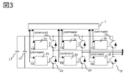
図3は、スイッチング素子2で構成されるインバータ8の具体的な構成の一例を示す図である。
インバータ8は、直流電源17及び平滑コンデンサ18の正極側と負極側との間に接続され、入力電流を直流電力と交流電力の間で変換して出力する。このために、インバータ8は、複数の半導体スイッチング素子(2a~2f)を備え、それぞれの出力線は、モータ9の3相(U相、V相及びW相)の巻き線に接続され、各半導体スイッチング素子(2a~2f)のオン・オフを制御して、モータ9と直流電源17との接続を制御する。
FIG. 3 is a diagram showing an example of a specific configuration of the
The
ゲート駆動回路3a~3fは、制御部1から送信されるPWM指令信号に基づき各半導体スイッチング素子(2a~2f)を駆動し、また、その駆動結果に基づき制御部1へフィードバック信号(FB)を送信する。
ここで、半導体スイッチング素子(2a~2f)としては、図示しているIGBTに限定するものではなく、トランジスタ、MOS-FET等、種々のスイッチング素子を採用できる。MOS-FETを用いた場合は、エミッタをソース、コレクタをドレインに読み替えることになる。
The
Here, the semiconductor switching element (2a to 2f) is not limited to the IGBT shown in the figure, and various switching elements such as a transistor and a MOS-FET can be adopted. When a MOS-FET is used, the emitter is read as the source and the collector is read as the drain.
図4は、PWM指令信号及びフィードバック信号(FB)からスイッチオフ遅延時間を算出するための制御部1の具体的な回路構成の一例を示す図である。
ゲート駆動回路3と制御部1とは、絶縁素子19a、19b(具体的には、光結合型素子、磁気結合型素子又は静電結合型素子等)によって絶縁されている。
FIG. 4 is a diagram showing an example of a specific circuit configuration of the
The
ゲート駆動回路3は、絶縁素子19aと19b、半導体スイッチング素子2を駆動するゲート駆動部20、ゲート電圧とスイッチオン参照電圧とを比較してスイッチオンを判定する比較器21及びゲート電圧とスイッチオフ参照電圧とを比較してスイッチオフを判定する比較器22から構成されている。比較器21及び比較器22の動作に基づいて、フィードバック信号(FB)がゲート駆動回路3から制御部1に送信される。
The
制御部1において、ゲート駆動回路3から受信したフィードバック信号(FB)は、内蔵する時間測定部23に入力され、フィードバック信号(FB)によるパルス幅が測定される。また、PWM変換部13から出力されたPWM指令信号は、ゲート駆動回路3のみならず、制御部1が内蔵する時間測定部24にも入力され、PWM指令信号パルス幅が測定される。ここで、時間測定部23及び時間測定部24は、例えば10n秒以下の時間分解能を持つ。時間測定部23及び時間測定部24で測定されたフィードバック信号(FB)及びPWM指令信号の各パルス幅それぞれは、時間比較部25に入力され、両方の値が比較されることでスイッチオフ遅延時間を算出することができる。
In the
また、上述の制御部1では、時間測定部23及び24により、フィードバック信号(FB)及びPWM指令信号の各パルス幅をそれぞれ測定したが、それらに替えて、PWM指令信号のスイッチオフからフィードバック信号(FB)のスイッチオフまでの時間を測定する別の時間測定部(図示せず)を設け、その測定時間に基づいてスイッチオフ遅延時間を算出するようにしてもよい。
Further, in the
図5は、PWM指令信号、ゲート電圧及びフィードバック信号(FB)、3者相互の時間的関係を示す図である。
図5に示すように、PWM変換部13から出力されたスイッチオンのPWM指令信号は、絶縁素子19bを含むゲート駆動回路3による回路遅延を経た後に、半導体スイッチング素子2のゲート端子にスイッチオン信号が入力される。半導体スイッチング素子2にスイッチオン信号が入力されると、ゲート抵抗と素子の容量に応じた時定数でゲート電圧が上昇する。ゲート電圧が該時定数による素子遅延を経てスイッチオン参照電圧に到達すると、比較器21が動作し、スイッチオンのフィードバック信号(FB)が出力される。フィードバック信号(FB)は、絶縁素子19aを含むゲート駆動回路3による回路遅延を経た後に、時間測定部23に入力される。
FIG. 5 is a diagram showing a PWM command signal, a gate voltage, a feedback signal (FB), and a temporal relationship between the three parties.
As shown in FIG. 5, the switch-on PWM command signal output from the
また同様に、スイッチオフのPWM指令信号がPWM変換部13から出力されると、絶縁素子19bを含むゲート駆動回路3による回路遅延を経た後に、半導体スイッチング素子2のゲート端子にスイッチオフ信号が入力される。半導体スイッチング素子2にスイッチオフ信号が入力されると、ゲート抵抗と素子の容量に応じた時定数でゲート電圧が下降する。ゲート電圧が該時定数による素子遅延を経てスイッチオフ参照電圧に到達すると、比較器22が動作し、スイッチオフのフィードバック信号(FB)が出力される。フィードバック信号(FB)は、絶縁素子19aを含むゲート駆動回路3による回路遅延を経た後に、時間測定部23に入力される。
Similarly, when the switch-off PWM command signal is output from the
時間測定部23は、スイッチオンのフィードバック信号(FB)及びスイッチオフのフィードバック信号(FB)の各入力に基づいて、フィードバック信号(FB)のパルス幅を測定する。
ここにおいて、発明者は、PWM指令信号、半導体スイッチング素子2のスイッチング波形及びフィードバック信号波形の相関を解析した。その結果、スイッチオンにおいて、素子遅延は、接合温度、コレクタ電流及び直流電源電圧に依存せずほぼ一定である。その一方で、スイッチオフにおいて、素子遅延は、接合温度、コレクタ電流及び直流電源電圧に依存して変化することを見出した。
The
Here, the inventor analyzed the correlation between the PWM command signal, the switching waveform of the
図6は、その(a)~(c)に、回路遅延時間を一定に揃えた条件の下で、スイッチオン時に、PWM指令信号出力時を基準時間とした場合のスイッチング波形を示す図である。
図6の(a)は接合温度を(例として、40℃及び100℃の場合)、図6の(b)はコレクタ電流を(例として、600A、900A及び1200Aの場合)、図6の(c)は直流電源電圧を(例として、1100V、1300V及び1500Vの場合)、様々に変えた場合の波形を示している。なお、スイッチオンを判定するスイッチオン参照電圧は、一例として5Vに設定している。
FIG. 6 is a diagram showing switching waveforms (a) to (c) when the switch is turned on and the PWM command signal is output as a reference time under the condition that the circuit delay time is made constant. ..
FIG. 6 (a) shows the junction temperature (for example, at 40 ° C. and 100 ° C.), FIG. 6 (b) shows the collector current (for example, at 600A, 900A, and 1200A), and FIG. 6 (for example). c) shows the waveform when the DC power supply voltage is changed in various ways (for example, in the case of 1100V, 1300V and 1500V). The switch-on reference voltage for determining the switch-on is set to 5V as an example.
図6(a)~(c)に示すように、接合温度、コレクタ電流及び直流電源電圧に依存せず、ゲート電圧がスイッチオン参照電圧に到達するタイミングは、ほとんど一定である。従って、スイッチオン時の素子遅延において、接合温度、コレクタ電流及び直流電源電圧に対する依存性は、非常に小さいことが分かる。 As shown in FIGS. 6A to 6C, the timing at which the gate voltage reaches the switch-on reference voltage is almost constant regardless of the junction temperature, collector current, and DC power supply voltage. Therefore, it can be seen that the dependence on the junction temperature, collector current, and DC power supply voltage in the element delay when the switch is turned on is very small.
図7は、その(a)~(f)に、回路遅延時間を一定に揃えた条件の下で、スイッチオフ時に、PWM指令信号出力時を基準時間とした場合のスイッチング波形((a)、(c)及び(e))とフィードバック信号波形((b)、(d)及び(f))を示す図である。
図7の(a)と(b)は接合温度を(例として、40℃及び100℃の場合)、図7の(c)と(d)はコレクタ電流を(例として、600A、900A及び1200Aの場合)、図7の(e)と(f)は直流電源電圧を(例として、1100V、1300V及び1500Vの場合)、様々に変えた場合の波形を示している。なお、スイッチオフを判定するスイッチオフ参照電圧は、一例として-5Vに設定している。
7 (a) and 7 show the switching waveforms ((a)) in the case where the circuit delay time is made constant and the PWM command signal output time is used as the reference time when the switch is turned off. It is a figure which shows (c) and (e)) and a feedback signal waveform ((b), (d) and (f)).
(A) and (b) of FIG. 7 refer to the junction temperature (for example, at 40 ° C. and 100 ° C.), and FIGS. 7 (c) and (d) refer to the collector current (for example, 600A, 900A and 1200A). In the case of), FIGS. 7 (e) and 7 (f) show waveforms when the DC power supply voltage is changed in various ways (for example, in the case of 1100V, 1300V and 1500V). The switch-off reference voltage for determining the switch-off is set to -5V as an example.
図7の(a)では接合温度が上昇すると、図7の(c)ではコレクタ電流が減少すると、また図7の(e)では直流電源電圧が上昇するとそれぞれ、ゲート電圧がスイッチオフ参照電圧に到達するまでの遅延時間は大きくなることが分かる。これらの現象は、主に素子の帰還容量の各パラメータに対する依存性で説明できることが知られている。
また、図7の(b)、(d)及び(f)に示すように、スイッチオフのフィードバック信号(FB)が出力されるタイミングは、ゲート電圧がスイッチオフ参照電圧に到達するまでの遅延時間に応じて変化することが分かる。
従って、スイッチオフ時の素子遅延は、接合温度、コレクタ電流及び直流電源電圧に依存して変化することが分かる。
When the junction temperature rises in (a) of FIG. 7, the collector current decreases in (c) of FIG. 7, and the DC power supply voltage rises in (e) of FIG. 7, the gate voltage becomes the switch-off reference voltage. It can be seen that the delay time to reach is large. It is known that these phenomena can be explained mainly by the dependence of the feedback capacitance of the device on each parameter.
Further, as shown in FIGS. 7 (b), (d) and (f), the timing at which the switch-off feedback signal (FB) is output is the delay time until the gate voltage reaches the switch-off reference voltage. It can be seen that it changes according to.
Therefore, it can be seen that the element delay at the time of switch-off changes depending on the junction temperature, collector current, and DC power supply voltage.
以上の結果により、PWM指令信号とフィードバック信号(FB)のパルス幅とを比較すれば、スイッチオフ時の素子遅延の変化を測定することができることを見出した。
回路遅延については、ゲート駆動回路3の雰囲気温度によって変化することを確認し、スイッチオン時の回路遅延の変化とスイッチオフ時の回路遅延の変化が同等であることを確認した。この結果により、PWM指令信号とフィードバック信号(FB)のパルス幅とを比較すれば、ゲート駆動回路による回路遅延の温度変化の影響を相殺できることを見出した。もし、スイッチオン時とスイッチオフ時の回路遅延の温度依存性が異なるような回路構成の場合は、ゲート駆動回路に温度計を設置するなどして、回路遅延の変化を補正すればよい。
From the above results, it has been found that the change in the element delay at the time of switch-off can be measured by comparing the pulse width of the PWM command signal and the feedback signal (FB).
It was confirmed that the circuit delay changed depending on the atmospheric temperature of the
上述の検討結果により、半導体スイッチング素子2の接合温度を推定するには、ターンオフ時の直流電源電圧及びコレクタ電流を検出し、上述の素子の遅延時間と検出した電流及び電圧との関係から、接合温度を算出する必要がある。
In order to estimate the junction temperature of the
直流電源電圧の検出に関しては、実施例1では、平滑コンデンサ18の正極側と負極側との電圧を測定して算出した。一方、コレクタ電流の検出に関しては、ターンオフ動作時にコレクタ電流が急激に変化するため、ターンオフのタイミングに合わせて電流をサンプリングすることは極めて困難である。また、図2に示すように、モータ制御用にモータ各相の電流をサンプリングしているが、一般的には、キャリア信号に同期してPWM指令信号のオン・オフの各中点でサンプリングされていることから、ターンオフのタイミングで電流を検出することがモータ制御には用いられていない。
Regarding the detection of the DC power supply voltage, in Example 1, the voltage between the positive electrode side and the negative electrode side of the smoothing
ここで発明者は、PWM指令信号、モータ制御用にキャリア信号に同期してサンプリングされたモータ相電流値及びターンオフ時のコレクタ電流の関係を解析した。その結果、各相のPWM指令信号の組み合わせによるモータ各相の電圧と、直流電源電圧、モータ誘起電圧Em及びモータ定数(インダクタンスL)に基づいて算出されるモータ相電流(ium、ivm及びiwm)の変化率と、キャリア同期によってサンプリングされたモータ相電流値と、またPWM指令信号のパルス幅と半導体スイッチング素子2の動作遅延による位相差とによって、ターンオフ時のコレクタ電流を推定できることを見出した。実施例1において、半導体スイッチング素子2の動作遅延は10μ秒以下であり、予め定数として設定したが、モータ相電流の変化率が小さい場合には動作遅延の影響を無視しても十分に電流精度を高くすることもできる。
Here, the inventor analyzed the relationship between the PWM command signal, the motor phase current value sampled in synchronization with the carrier signal for motor control, and the collector current at turn-off. As a result, the motor phase currents (ium, ivm and iwm) calculated based on the voltage of each phase of the motor by the combination of the PWM command signals of each phase, the DC power supply voltage, the motor induced voltage Em and the motor constant (intravenous L). It has been found that the collector current at turn-off can be estimated from the rate of change of, the motor phase current value sampled by carrier synchronization, and the phase difference between the pulse width of the PWM command signal and the operation delay of the
図8は、PWM指令信号、キャリア信号、モータ相電流(Im)、モータ制御用に検出されたモータ電流値(電流サンプル)及びターンオフ時の推定コレクタ電流、それぞれの関係を示す図である。
実施例1では、上述の関係を用いて、PWM指令信号幅やキャリア周期等の制御用の内部パラメータ及びモータ相電流を電流算出部4に入力し、ターンオフ時のコレクタ電流を算出している。実施例1によれば、従来から用いられていたモータ制御用に検出した電流値を用いて、ターンオフ時のコレクタ電流を精度良く推定することができる。
FIG. 8 is a diagram showing the relationship between a PWM command signal, a carrier signal, a motor phase current (Im), a motor current value (current sample) detected for motor control, and an estimated collector current at turn-off.
In the first embodiment, the internal parameters for control such as the PWM command signal width and the carrier cycle and the motor phase current are input to the
図9は、スイッチオフ遅延に関して、その(a)に半導体スイッチング素子2の接合温度(Tj)との関係、その(b)にコレクタ電流(Ice)との関係、その(c)に直流電源電圧(Vce)との関係、それぞれを示している。
また、状態監視部6には、時間比較部25により算出されたスイッチオフ遅延時間と、電流算出部4によって算出されたターンオフ時の推定コレクタ電流と、電圧算出部5によって算出されたターンオフ時の直流電源電圧とが入力され、これらの遅延時間と電流及び電圧との関係から、スイッチング毎に半導体スイッチング素子2の接合温度が推定される。その様子を、例示的に図9の(d)に示す。
In FIG. 9, regarding the switch-off delay, (a) has a relationship with the junction temperature (Tj) of the
Further, the
以上のように、実施例1の着眼点の一つは、電力変換装置内の複数の半導体スイッチング素子2の摩耗度を監視し、システムの故障を未然に防止し、適切な機器更新の時期を通知するものである。
As described above, one of the points of focus of the first embodiment is to monitor the degree of wear of a plurality of
図10は、モータ相電流の経時変化及び接合温度が最大と最少になる点を示す図である。
状態監視部6は、例えば図10に示すように、各モータ相電流(Im)の一周期において、最大値(Tmax)及び最小値(Tmin)でのスイッチング動作時の接合温度を監視し、その温度差と回数を熱サイクルの頻度分布としてメモリ等に記憶する手段を有する。この熱サイクルを頻度に変換する方法としては、例えばレインフローアルゴリズムがある。
FIG. 10 is a diagram showing the time course of the motor phase current and the points where the junction temperature becomes the maximum and the minimum.
As shown in FIG. 10, for example, the
図11は、接合温度の時系列データとヒストグラムに変換した温度振幅頻度の例を示す図である。横軸の温度振幅ΔTは、例えば5℃刻みで設定する。縦軸は、サイクル数Nの対数表示(logN)である。熱サイクル定格としては、半導体スイッチング素子2の出荷時に提供されるパワーサイクル試験を用いる。図11において、Niは、温度振幅Tiの許容最大サイクル数、ni(図11に示す黒塗り部分)は、状態監視部6によって得られた温度振幅Tiのサイクル数である。また、各温度振幅Tiの摩耗度Diは、ni/Niで与えられ、全体の摩耗度は、ΣDiで与えられる。
FIG. 11 is a diagram showing an example of the time series data of the joining temperature and the temperature amplitude frequency converted into a histogram. The temperature amplitude ΔT on the horizontal axis is set, for example, in increments of 5 ° C. The vertical axis is a logarithmic display (logN) of the number of cycles N. As the thermal cycle rating, the power cycle test provided at the time of shipment of the
状態監視部6で算出されたΣDiは、異常診断部7に送信される。異常診断部7は、入力されたΣDiが規定値を超過した場合に素子の摩耗劣化を判定し、判定結果を関係者に通知する。その際に、異常診断部7は、機器更新を促すGUI(Graphical User Interface)を備えてもよい。また、異常判定結果は、車両情報統合システムに送信することもでき、さらに、中央監視システムに含めれば、複数の車両の監視が可能となり、保全計画の最適化に寄与させることができる。
The ΣDi calculated by the
以上のとおり、実施例1によれば、半導体スイッチング素子の接合温度変化の時系列データを蓄積し、基準値と比較判定することによって、半導体スイッチング素子及びこれに関連する電力変換装置の摩耗度を高精度に検出し、故障などの不具合を高精度に防ぐと共に、機器更新や保全の最適化を図ることが可能である。 As described above, according to the first embodiment, the degree of wear of the semiconductor switching element and the power conversion device related thereto is determined by accumulating the time-series data of the junction temperature change of the semiconductor switching element and comparing and determining it with the reference value. It is possible to detect with high accuracy, prevent defects such as failures with high accuracy, and optimize equipment update and maintenance.
実施例2は、本発明に係る構成を用いて、電力変換装置に発生する突発的な異常を検知する方法を提供する。具体的には、電力変換装置の地絡等による電流値の異常の検知方法であって、以下にその方法について説明する。
図12は、その(a)に、正常動作時及び地絡発生時のモータ相電流(Im)の変化を示し、その(b)に、スイッチオフ遅延時間と算出された推定接合温度(Tj)との関係を示す図である。
The second embodiment provides a method for detecting a sudden abnormality occurring in a power conversion device by using the configuration according to the present invention. Specifically, it is a method for detecting an abnormality in the current value due to a ground fault or the like of a power conversion device, and the method will be described below.
FIG. 12 shows the change in the motor phase current (Im) during normal operation and when a ground fault occurs in (a), and in (b), the switch-off delay time and the calculated estimated junction temperature (Tj). It is a figure which shows the relationship with.
図12の(a)に示すように、地絡が発生するとモータ相電流(Im)の変化率が正常動作時に比べて大きくなるため、電流算出部4で算出したコレクタ電流の推定値よりも、実際に半導体スイッチング素子2を通電するコレクタ電流は大きくなる。
その結果、図12の(b)に示すように、地絡が発生した場合はスイッチオフ遅延時間が正常動作時に比べて短くなるため、スイッチオフ遅延時間とコレクタ電流及びコレクタ電圧の各推定値に基づいて、状態監視部6で推定される半導体スイッチング素子2の接合温度(Tj)は正常動作時と比較して低く推定される。また、スイッチオフ遅延時間の電流依存性が大きいため、状態監視部6では半導体スイッチング素子2の接合温度(Tj)は急激に低下した異常な結果を出力する。
As shown in FIG. 12 (a), when a ground fault occurs, the rate of change of the motor phase current (Im) becomes larger than that during normal operation, so that the estimated value of the collector current calculated by the
As a result, as shown in FIG. 12B, when a ground fault occurs, the switch-off delay time becomes shorter than that during normal operation. Therefore, the switch-off delay time and the estimated values of the collector current and the collector voltage are used. Based on this, the junction temperature (Tj) of the
以上のことから、スイッチオフ遅延時間、コレクタ電流及びコレクタ電圧の各推定値に基づいて、地絡等によるコレクタ電流値の異常判定することができる。
実施例2によれば、状態監視部6から異常監視部7に入力された接合温度(Tj)の時系列データにおいて、接合温度変化が所定の値より大きい異常な値を出力した場合に電流値の異常を判定することができる。
From the above, it is possible to determine an abnormality in the collector current value due to a ground fault or the like based on the estimated values of the switch-off delay time, the collector current, and the collector voltage.
According to the second embodiment, in the time series data of the junction temperature (Tj) input from the
一般的には、地絡や短絡の検知は、予め参照電流値を設け、この参照電流値を超過した過電流状態となった場合に検知するため、検知タイミングが遅れる課題があった。実施例2による地絡検知では、過電流状態に至らない低電流領域での動作においてもスイッチング毎に異常の有無を判定することができるため、システムの保護をより早期に実施できる長所がある。
従って、実施例2に係る異常検知方法によって、システムの損傷を防止あるいは軽減することが可能となる。
In general, the detection of a ground fault or a short circuit has a problem that the detection timing is delayed because the reference current value is set in advance and the detection is performed when the overcurrent state exceeds the reference current value. The ground fault detection according to the second embodiment has an advantage that the protection of the system can be carried out earlier because it is possible to determine the presence or absence of an abnormality for each switching even in the operation in the low current region where the overcurrent state does not occur.
Therefore, the abnormality detection method according to the second embodiment can prevent or reduce damage to the system.
実施例3は、本発明に係る構成を用いて、電力変換装置に発生する突発的な異常を検知する別の方法を提供する。具体的には、ゲート駆動回路の誤動作の検知方法であって、以下にその検知方法について説明する。
図13は、実施例3に係る制御部1の一部の構成を、ゲート駆動回路3と共に示す図である。
先の実施例1では、時間測定部23及び24により、フィードバック信号(FB)及びPWM指令信号の各パルス幅をそれぞれ測定し、時間比較部25にてスイッチオフ遅延時間を算出した。実施例3においては、先の実施例1の構成に加えてさらにパルス回数測定部26を備え、時間測定部23及び24の出力結果に基づいてフィードバック信号(FB)及びPWM指令信号の各パルス回数をカウントすることを特徴とする。
The third embodiment provides another method for detecting a sudden abnormality occurring in a power conversion device by using the configuration according to the present invention. Specifically, it is a method of detecting a malfunction of a gate drive circuit, and the detection method will be described below.
FIG. 13 is a diagram showing a partial configuration of the
In the first embodiment, the
図14は、実施例3に係るパルス回数測定部26によりカウントされたPWM信号及びフィードバック信号(FB)の各パルス数の関係を示す図である。
ゲート駆動回路3は、周辺環境や電力変換装置自身の動作の影響を受けて誤動作する可能性があることが知られている。ゲート駆動回路3が誤動作によって意図せずに動作すると、電力変換装置の短絡が発生する場合があり、システムが損傷する懸念がある。
FIG. 14 is a diagram showing the relationship between the number of pulses of the PWM signal and the feedback signal (FB) counted by the pulse
It is known that the
そこで、一般的にはPWM指令信号及びフィードバック信号の各出力を比較し、ゲート駆動回路が正常に動作しているかを監視し、PWM指令信号及びフィードバック信号の各出力の不一致期間が所定の値より大きい場合に、ゲート駆動回路の誤動作を判定する。
しかしながら、図5に示すように、正常動作時において、PWM指令信号とフィードバック信号との間には、回路遅延や素子遅延による動作遅延が存在するため、異常判定のための出力不一致期間の閾値を大きくする必要がある。このように、出力不一致期間の閾値を大きくすると、短期間の誤動作を検出できないため、システムに劣化や損傷をもたらす懸念がある。
Therefore, in general, the outputs of the PWM command signal and the feedback signal are compared to monitor whether the gate drive circuit is operating normally, and the mismatch period between the outputs of the PWM command signal and the feedback signal is more than a predetermined value. If it is large, the malfunction of the gate drive circuit is determined.
However, as shown in FIG. 5, during normal operation, there is an operation delay due to a circuit delay or an element delay between the PWM command signal and the feedback signal, so the threshold value of the output mismatch period for abnormality determination is set. It needs to be large. As described above, if the threshold value of the output mismatch period is increased, a short-term malfunction cannot be detected, and there is a concern that the system may be deteriorated or damaged.
実施例3によれば、PWM指令信号及びフィードバック信号(FB)の各パルス数の比較に基づいて、ゲート駆動回路3の誤動作を検出するため、短期間の誤動作の検出が可能になる長所がある。さらに、図14に示すように、時間測定部23でフィードバック信号(FB)のパルス幅も測定可能であるため、誤動作期間を検出することも可能である。
従って、実施例3に係る異常検知方法によって、システムの損傷を防止あるいは軽減することが可能となる。
According to the third embodiment, since the malfunction of the
Therefore, the abnormality detection method according to the third embodiment can prevent or reduce damage to the system.
1…制御部、2(2a~2f)…半導体スイッチング素子、
3(3a~3f)…ゲート駆動回路、4…電流算出部、5…電圧算出部、
6…状態監視部、7…異常診断部、8…インバータ、9…モータ、
10…トルク指令算出部、11…電流指令算出部、
12…電流指令/3相電圧指令変換部、13…PWM変換部、
14…電流帰還変換部、15…PWM指令信号幅算出部、
16…フィードバック信号幅算出部、17…直流電源、18…平滑コンデンサ、
19(19a・19b)…絶縁素子、20…ゲート駆動部、21・22…比較器、
23・24…時間測定部、25…時間比較部、26…パルス回数測定部
1 ... Control unit, 2 (2a to 2f) ... Semiconductor switching element,
3 (3a to 3f) ... Gate drive circuit, 4 ... Current calculation unit, 5 ... Voltage calculation unit,
6 ... Condition monitoring unit, 7 ... Abnormality diagnosis unit, 8 ... Inverter, 9 ... Motor,
10 ... Torque command calculation unit, 11 ... Current command calculation unit,
12 ... Current command / 3-phase voltage command conversion unit, 13 ... PWM conversion unit,
14 ... Current feedback conversion unit, 15 ... PWM command signal width calculation unit,
16 ... Feedback signal width calculation unit, 17 ... DC power supply, 18 ... Smoothing capacitor,
19 (19a / 19b) ... Insulation element, 20 ... Gate drive unit, 21.22 ... Comparator,
23/24 ... Time measurement unit, 25 ... Time comparison unit, 26 ... Pulse count measurement unit
Claims (14)
前記スイッチング素子を駆動するためのPWM指令信号に基づいて前記スイッチング素子を駆動するゲート駆動回路と、
前記スイッチング素子がターンオフするタイミングにおける、コレクタ電流又はドレイン電流及びコレクタ電圧又はドレイン電圧をそれぞれ推定するための算出を行う電流算出部及び電圧算出部と、
前記PWM指令信号、前記スイッチング素子のスイッチング動作に伴って生成するフィードバック信号、前記コレクタ電流又は前記ドレイン電流の推定電流及び前記コレクタ電圧又は前記ドレイン電圧の推定電圧に基づいて、前記電力変換装置の運転状態を推定する状態監視部と、
前記状態監視部が推定した前記電力変換装置の運転状態に基づいて当該電力変換装置の異常を判定する異常診断部と、
前記PWM指令信号のオン期間又はオフ期間を測定する第1の時間測定部と、
前記フィードバック信号のオン期間又はオフ期間を測定する第2の時間測定部と
を備え、
前記第1の時間測定部により測定された前記PWM指令信号のオン期間又はオフ期間と、前記第2の時間測定部により測定された前記フィードバック信号のオン期間又はオフ期間とに基づいて、前記スイッチング素子のスイッチオフ遅延時間を算出する
ことを特徴とする電力変換装置。 A power conversion device having a switching element.
A gate drive circuit that drives the switching element based on a PWM command signal for driving the switching element, and a gate drive circuit.
A current calculation unit and a voltage calculation unit that perform calculations for estimating the collector current or drain current and the collector voltage or drain voltage at the timing at which the switching element turns off, respectively.
The operation of the power conversion device is based on the PWM command signal, the feedback signal generated by the switching operation of the switching element, the estimated current of the collector current or the drain current, and the estimated voltage of the collector voltage or the drain voltage. A state monitoring unit that estimates the state, and a state monitoring unit
An abnormality diagnosis unit that determines an abnormality in the power conversion device based on the operating state of the power conversion device estimated by the condition monitoring unit, and an abnormality diagnosis unit .
A first time measuring unit for measuring an on period or an off period of the PWM command signal, and
With a second time measuring unit that measures the on period or off period of the feedback signal
Equipped with
The switching is based on the on / off period of the PWM command signal measured by the first time measuring unit and the on / off period of the feedback signal measured by the second time measuring unit. Calculate the switch-off delay time of the element
A power conversion device characterized by that .
前記フィードバック信号は、前記スイッチング素子のスイッチング動作時におけるゲートとエミッタ又はソースとの間の電圧と、スイッチオン参照電圧及びスイッチオフ参照電圧とをそれぞれ比較することにより生成される
ことを特徴とする電力変換装置。 The power conversion device according to claim 1.
The feedback signal is a power generated by comparing a voltage between a gate and an emitter or a source during a switching operation of the switching element with a switch-on reference voltage and a switch-off reference voltage, respectively. Converter.
前記電圧算出部は、前記電力変換装置の直流電源側の正極と負極との間に設けたコンデンサの測定電圧に基づいて前記コレクタ電圧又は前記ドレイン電圧の推定電圧を算出する
ことを特徴とする電力変換装置。 The power conversion device according to claim 1 or 2.
The voltage calculation unit calculates the estimated voltage of the collector voltage or the drain voltage based on the measured voltage of the capacitor provided between the positive electrode and the negative electrode on the DC power supply side of the power conversion device.
A power conversion device characterized by that.
前記電流算出部は、前記電力変換装置が出力する各相電流の測定電流、前記PWM指令信号及び前記コレクタ電圧又は前記ドレイン電圧の推定電圧に基づいて、前記スイッチング素子がスイッチオフするタイミングにおける前記コレクタ電流又は前記ドレイン電流の推定電流を算出する
ことを特徴とする電力変換装置。 The power conversion device according to any one of claims 1 to 3 .
The current calculation unit is based on the measured current of each phase current output by the power conversion device, the PWM command signal, and the estimated voltage of the collector voltage or the drain voltage, and the collector at the timing when the switching element is switched off. Calculate the estimated current of the current or the drain current
A power conversion device characterized by that.
前記状態監視部は、前記スイッチオフ遅延時間、前記コレクタ電流又は前記ドレイン電流の推定電流及び前記コレクタ電圧又は前記ドレイン電圧の推定電圧に基づいて、前記スイッチング素子の接合温度を算出する
ことを特徴とする電力変換装置。 The power conversion device according to any one of claims 1 to 4.
The condition monitoring unit calculates the junction temperature of the switching element based on the switch-off delay time, the estimated current of the collector current or the drain current, and the estimated voltage of the collector voltage or the drain voltage.
A power conversion device characterized by that.
前記状態監視部は、算出された前記接合温度の時系列データから当該接合温度が変化する温度振幅及び当該接合温度が当該温度振幅で変化する回数を算出し、当該温度振幅と当該回数に基づいて前記スイッチング素子の摩耗度を算出する
ことを特徴とする電力変換装置。 The power conversion device according to claim 5 .
The condition monitoring unit calculates the temperature amplitude at which the junction temperature changes and the number of times the junction temperature changes with the temperature amplitude from the calculated time-series data of the junction temperature, and based on the temperature amplitude and the number of times. Calculate the degree of wear of the switching element
A power conversion device characterized by that.
前記異常診断部は、前記スイッチオフ遅延時間、前記コレクタ電圧又は前記ドレイン電圧の推定電圧及び前記コレクタ電流又は前記ドレイン電流の推定電流に基づいて、前記コレクタ電流又は前記ドレイン電流の電流値の異常を判定する
ことを特徴とする電力変換装置。 The power conversion device according to any one of claims 1 to 6 .
The abnormality diagnosis unit detects an abnormality in the current value of the collector current or the drain current based on the switch-off delay time, the estimated voltage of the collector voltage or the drain voltage, and the estimated current of the collector current or the drain current. judge
A power conversion device characterized by that.
前記PWM指令信号のパルス回数及び前記フィードバック信号のパルス回数をそれぞれ測定するパルス回数測定部を備え、測定されたそれぞれの前記パルス回数の比較結果に基づいて前記ゲート駆動回路の誤動作を検知する
ことを特徴とする電力変換装置。 The power conversion device according to any one of claims 1 to 7 .
A pulse number measuring unit for measuring the number of pulses of the PWM command signal and the number of pulses of the feedback signal is provided, and a malfunction of the gate drive circuit is detected based on the comparison result of each measured number of pulses.
A power conversion device characterized by that.
前記スイッチング素子を駆動するためのPWM指令信号、前記スイッチング素子のスイッチング動作に伴って生成するフィードバック信号、前記コレクタ電流又は前記ドレイン電流の推定電流及び前記コレクタ電圧又は前記ドレイン電圧の推定電圧に基づいて、前記電力変換装置の運転状態を推定する第2のステップと、Based on the PWM command signal for driving the switching element, the feedback signal generated by the switching operation of the switching element, the estimated current of the collector current or the drain current, and the estimated voltage of the collector voltage or the drain voltage. , The second step of estimating the operating state of the power converter,
推定した前記電力変換装置の運転状態に基づいて当該電力変換装置の異常を判定する第3のステップと、A third step of determining an abnormality of the power conversion device based on the estimated operating state of the power conversion device, and
前記PWM指令信号のオン期間又はオフ期間及び前記フィードバック信号のオン期間又はオフ期間を測定する第4のステップと、The fourth step of measuring the on period or off period of the PWM command signal and the on period or off period of the feedback signal, and
測定した前記PWM指令信号のオン期間又はオフ期間と、測定した前記フィードバック信号のオン期間又はオフ期間とに基づいて、前記スイッチング素子のスイッチオフ遅延時間を算出する第5のステップとA fifth step of calculating the switch-off delay time of the switching element based on the measured on-period or off-period of the PWM command signal and the on-period or off-period of the measured feedback signal.
を有する電力変換装置の診断方法。A method of diagnosing a power converter having.
前記フィードバック信号を、前記スイッチング素子のスイッチング動作時におけるゲートとエミッタ又はソースとの間の電圧と、スイッチオン参照電圧及びスイッチオフ参照電圧とをそれぞれ比較することにより生成するThe feedback signal is generated by comparing the voltage between the gate and the emitter or source during the switching operation of the switching element with the switch-on reference voltage and the switch-off reference voltage, respectively.
ことを特徴とする電力変換装置の診断方法。A method of diagnosing a power converter, which is characterized by the fact that.
前記スイッチオフ遅延時間、前記コレクタ電流又は前記ドレイン電流の推定電流及び前記コレクタ電圧又は前記ドレイン電圧の推定電圧に基づいて、前記スイッチング素子の接合温度を算出する第6のステップ
を更に有する電力変換装置の診断方法。 The method for diagnosing a power conversion device according to claim 9 or 10.
A sixth step of calculating the junction temperature of the switching element based on the switch-off delay time, the estimated current of the collector current or the drain current, and the estimated voltage of the collector voltage or the drain voltage.
A method of diagnosing a power conversion device having the above.
算出された前記接合温度の時系列データから前記接合温度が変化する温度振幅及び当該接合温度が当該温度振幅で変化する回数を算出し、当該温度振幅と当該回数に基づいて前記スイッチング素子の摩耗度を算出する第7のステップ
を更に有する電力変換装置の診断方法。 The method for diagnosing the power conversion device according to claim 11.
From the calculated time-series data of the junction temperature, the temperature amplitude at which the junction temperature changes and the number of times the junction temperature changes with the temperature amplitude are calculated, and the degree of wear of the switching element is calculated based on the temperature amplitude and the number of times. 7th step to calculate
A method of diagnosing a power conversion device having the above.
前記スイッチオフ遅延時間、前記コレクタ電圧又は前記ドレイン電圧の推定電圧及び前記コレクタ電流又は前記ドレイン電流の推定電流に基づいて、前記コレクタ電流又は前記ドレイン電流の電流値の異常を判定する第8のステップ
を更に有する電力変換装置の診断方法。 The method for diagnosing a power conversion device according to any one of claims 9 to 12 .
Eighth step to determine an abnormality in the current value of the collector current or the drain current based on the switch-off delay time, the estimated voltage of the collector voltage or the drain voltage, and the estimated current of the collector current or the drain current.
A method of diagnosing a power conversion device having the above.
前記PWM指令信号のパルス回数及び前記フィードバック信号のパルス回数をそれぞれ測定する第9のステップと、
測定したそれぞれの前記パルス回数の比較結果に基づいて前記スイッチング素子のゲート駆動回路の誤動作を検知する第10のステップと
を更に有する電力変換装置の診断方法。
The method for diagnosing a power conversion device according to any one of claims 9 to 13 .
A ninth step of measuring the number of pulses of the PWM command signal and the number of pulses of the feedback signal, respectively.
The tenth step of detecting the malfunction of the gate drive circuit of the switching element based on the comparison result of the measured number of pulses.
A method of diagnosing a power conversion device having the above.
Priority Applications (2)
| Application Number | Priority Date | Filing Date | Title |
|---|---|---|---|
| JP2018196372A JP7085453B2 (en) | 2018-10-18 | 2018-10-18 | Diagnostic method for power converters and power converters |
| CN201910985749.9A CN111092563B (en) | 2018-10-18 | 2019-10-17 | Power conversion device and diagnosis method for power conversion device |
Applications Claiming Priority (1)
| Application Number | Priority Date | Filing Date | Title |
|---|---|---|---|
| JP2018196372A JP7085453B2 (en) | 2018-10-18 | 2018-10-18 | Diagnostic method for power converters and power converters |
Publications (2)
| Publication Number | Publication Date |
|---|---|
| JP2020065386A JP2020065386A (en) | 2020-04-23 |
| JP7085453B2 true JP7085453B2 (en) | 2022-06-16 |
Family
ID=70387649
Family Applications (1)
| Application Number | Title | Priority Date | Filing Date |
|---|---|---|---|
| JP2018196372A Active JP7085453B2 (en) | 2018-10-18 | 2018-10-18 | Diagnostic method for power converters and power converters |
Country Status (2)
| Country | Link |
|---|---|
| JP (1) | JP7085453B2 (en) |
| CN (1) | CN111092563B (en) |
Families Citing this family (1)
| Publication number | Priority date | Publication date | Assignee | Title |
|---|---|---|---|---|
| CN111352003B (en) * | 2020-05-25 | 2020-08-21 | 北京中航科电测控技术股份有限公司 | Analysis system for electrical equipment faults |
Citations (6)
| Publication number | Priority date | Publication date | Assignee | Title |
|---|---|---|---|---|
| WO2007034544A1 (en) | 2005-09-21 | 2007-03-29 | Mitsubishi Denki Kabushiki Kaisha | Excessive-temperature detection system of motor controller |
| JP2009201311A (en) | 2008-02-25 | 2009-09-03 | Hitachi Ltd | Control device for power converter |
| US20130177041A1 (en) | 2012-01-11 | 2013-07-11 | Abb Research Ltd | System and method for monitoring in real time the operating state of an igbt device |
| WO2016042970A1 (en) | 2014-09-19 | 2016-03-24 | 株式会社日立製作所 | Power conversion device |
| JP2017118792A (en) | 2015-12-25 | 2017-06-29 | 株式会社東芝 | Control circuit |
| JP2018011250A (en) | 2016-07-15 | 2018-01-18 | 富士電機株式会社 | Semiconductor device |
Family Cites Families (6)
| Publication number | Priority date | Publication date | Assignee | Title |
|---|---|---|---|---|
| JPH07170724A (en) * | 1993-12-10 | 1995-07-04 | Toshiba Corp | Drive circuit for switching element |
| JPH1097497A (en) * | 1996-09-19 | 1998-04-14 | N T T Data Tsushin Kk | Interface checker and circuit inspecting method |
| JP3886876B2 (en) * | 2002-01-17 | 2007-02-28 | 三菱電機株式会社 | Power semiconductor element drive circuit |
| JP2013055801A (en) * | 2011-09-05 | 2013-03-21 | Nissan Motor Co Ltd | Power conversion device |
| JP6117744B2 (en) * | 2014-07-11 | 2017-04-19 | ファナック株式会社 | Motor drive device having dead band width estimation function of output stage |
| US10700678B2 (en) * | 2015-06-16 | 2020-06-30 | Mitsubishi Electric Corporation | Drive control circuit for power semiconductor element |
-
2018
- 2018-10-18 JP JP2018196372A patent/JP7085453B2/en active Active
-
2019
- 2019-10-17 CN CN201910985749.9A patent/CN111092563B/en active Active
Patent Citations (7)
| Publication number | Priority date | Publication date | Assignee | Title |
|---|---|---|---|---|
| WO2007034544A1 (en) | 2005-09-21 | 2007-03-29 | Mitsubishi Denki Kabushiki Kaisha | Excessive-temperature detection system of motor controller |
| JP2009201311A (en) | 2008-02-25 | 2009-09-03 | Hitachi Ltd | Control device for power converter |
| US20130177041A1 (en) | 2012-01-11 | 2013-07-11 | Abb Research Ltd | System and method for monitoring in real time the operating state of an igbt device |
| JP2013142704A (en) | 2012-01-11 | 2013-07-22 | Abb Research Ltd | System and method for monitoring operation state of igbt device in real time |
| WO2016042970A1 (en) | 2014-09-19 | 2016-03-24 | 株式会社日立製作所 | Power conversion device |
| JP2017118792A (en) | 2015-12-25 | 2017-06-29 | 株式会社東芝 | Control circuit |
| JP2018011250A (en) | 2016-07-15 | 2018-01-18 | 富士電機株式会社 | Semiconductor device |
Also Published As
| Publication number | Publication date |
|---|---|
| CN111092563A (en) | 2020-05-01 |
| JP2020065386A (en) | 2020-04-23 |
| CN111092563B (en) | 2023-10-10 |
Similar Documents
| Publication | Publication Date | Title |
|---|---|---|
| US9935577B2 (en) | Semiconductor device and fault detecting method | |
| JP6853147B2 (en) | Diagnostic methods for power converters, motor control systems, and power converters | |
| EP2424064B1 (en) | Overcurrent fault detection device for electrical drive control system | |
| EP3197036B1 (en) | Power conversion device | |
| JP6699253B2 (en) | Power conversion device, switching element short-circuit failure diagnosis method, and switching element open failure diagnosis method | |
| CN101142737A (en) | Superheating detection mode of electric motor control device | |
| WO2017195247A1 (en) | Diagnosis system for power conversion device, diagnosis method for semiconductor module, and power conversion device | |
| JP4772104B2 (en) | Power converter | |
| JP6825975B2 (en) | Power converter, its diagnostic system, diagnostic method, and motor control system using it | |
| KR101142973B1 (en) | Apparatus and method for diagnosing electrical contact quality of motor, and a medium having computer readable program for executing the method | |
| JP7085453B2 (en) | Diagnostic method for power converters and power converters | |
| JP5422909B2 (en) | Power converter | |
| WO2019198775A1 (en) | Diagnostic device and diagnostic system | |
| KR101259623B1 (en) | Apparatus for controlling inverter current and Method for operating the same | |
| JP2010252576A (en) | Current controller | |
| JP6714767B2 (en) | Power converter diagnostic circuit, power converter diagnostic system | |
| WO2017085825A1 (en) | Power conversion device and vehicle control system | |
| JP7072497B2 (en) | Power converter and its status monitoring method | |
| Oelkers et al. | Oversampling based approach for open circuit fault detection in PMSM drive systems | |
| JP2019187055A (en) | Power conversion device and diagnostic system of power conversion device |
Legal Events
| Date | Code | Title | Description |
|---|---|---|---|
| A621 | Written request for application examination |
Free format text: JAPANESE INTERMEDIATE CODE: A621 Effective date: 20210326 |
|
| A977 | Report on retrieval |
Free format text: JAPANESE INTERMEDIATE CODE: A971007 Effective date: 20220126 |
|
| A131 | Notification of reasons for refusal |
Free format text: JAPANESE INTERMEDIATE CODE: A131 Effective date: 20220201 |
|
| A521 | Request for written amendment filed |
Free format text: JAPANESE INTERMEDIATE CODE: A523 Effective date: 20220301 |
|
| TRDD | Decision of grant or rejection written | ||
| A01 | Written decision to grant a patent or to grant a registration (utility model) |
Free format text: JAPANESE INTERMEDIATE CODE: A01 Effective date: 20220531 |
|
| A61 | First payment of annual fees (during grant procedure) |
Free format text: JAPANESE INTERMEDIATE CODE: A61 Effective date: 20220606 |
|
| R150 | Certificate of patent or registration of utility model |
Ref document number: 7085453 Country of ref document: JP Free format text: JAPANESE INTERMEDIATE CODE: R150 |