JP7080867B2 - Sn-Bi-In system low melting point bonding member, micro member and semiconductor electronic circuit, bump manufacturing method and semiconductor electronic circuit mounting method - Google Patents
Sn-Bi-In system low melting point bonding member, micro member and semiconductor electronic circuit, bump manufacturing method and semiconductor electronic circuit mounting method Download PDFInfo
- Publication number
- JP7080867B2 JP7080867B2 JP2019165701A JP2019165701A JP7080867B2 JP 7080867 B2 JP7080867 B2 JP 7080867B2 JP 2019165701 A JP2019165701 A JP 2019165701A JP 2019165701 A JP2019165701 A JP 2019165701A JP 7080867 B2 JP7080867 B2 JP 7080867B2
- Authority
- JP
- Japan
- Prior art keywords
- plating
- melting point
- low melting
- plated
- mass
- Prior art date
- Legal status (The legal status is an assumption and is not a legal conclusion. Google has not performed a legal analysis and makes no representation as to the accuracy of the status listed.)
- Active
Links
Images


Classifications
-
- H—ELECTRICITY
- H01—ELECTRIC ELEMENTS
- H01L—SEMICONDUCTOR DEVICES NOT COVERED BY CLASS H10
- H01L2224/00—Indexing scheme for arrangements for connecting or disconnecting semiconductor or solid-state bodies and methods related thereto as covered by H01L24/00
- H01L2224/01—Means for bonding being attached to, or being formed on, the surface to be connected, e.g. chip-to-package, die-attach, "first-level" interconnects; Manufacturing methods related thereto
- H01L2224/10—Bump connectors; Manufacturing methods related thereto
- H01L2224/11—Manufacturing methods
-
- H—ELECTRICITY
- H01—ELECTRIC ELEMENTS
- H01L—SEMICONDUCTOR DEVICES NOT COVERED BY CLASS H10
- H01L2224/00—Indexing scheme for arrangements for connecting or disconnecting semiconductor or solid-state bodies and methods related thereto as covered by H01L24/00
- H01L2224/01—Means for bonding being attached to, or being formed on, the surface to be connected, e.g. chip-to-package, die-attach, "first-level" interconnects; Manufacturing methods related thereto
- H01L2224/10—Bump connectors; Manufacturing methods related thereto
- H01L2224/15—Structure, shape, material or disposition of the bump connectors after the connecting process
- H01L2224/16—Structure, shape, material or disposition of the bump connectors after the connecting process of an individual bump connector
- H01L2224/161—Disposition
- H01L2224/16151—Disposition the bump connector connecting between a semiconductor or solid-state body and an item not being a semiconductor or solid-state body, e.g. chip-to-substrate, chip-to-passive
- H01L2224/16221—Disposition the bump connector connecting between a semiconductor or solid-state body and an item not being a semiconductor or solid-state body, e.g. chip-to-substrate, chip-to-passive the body and the item being stacked
- H01L2224/16225—Disposition the bump connector connecting between a semiconductor or solid-state body and an item not being a semiconductor or solid-state body, e.g. chip-to-substrate, chip-to-passive the body and the item being stacked the item being non-metallic, e.g. insulating substrate with or without metallisation
-
- H—ELECTRICITY
- H01—ELECTRIC ELEMENTS
- H01L—SEMICONDUCTOR DEVICES NOT COVERED BY CLASS H10
- H01L2224/00—Indexing scheme for arrangements for connecting or disconnecting semiconductor or solid-state bodies and methods related thereto as covered by H01L24/00
- H01L2224/80—Methods for connecting semiconductor or other solid state bodies using means for bonding being attached to, or being formed on, the surface to be connected
- H01L2224/81—Methods for connecting semiconductor or other solid state bodies using means for bonding being attached to, or being formed on, the surface to be connected using a bump connector
- H01L2224/8119—Arrangement of the bump connectors prior to mounting
- H01L2224/81191—Arrangement of the bump connectors prior to mounting wherein the bump connectors are disposed only on the semiconductor or solid-state body
Landscapes
- Electric Connection Of Electric Components To Printed Circuits (AREA)
Description
本発明は、半導体実装時の鉛フリーはんだ材料に関し、特に低温領域で使用可能なSn-Bi-In系接合部材に関する。 The present invention relates to a lead-free solder material for semiconductor mounting, and particularly to a Sn-Bi-In-based joining member that can be used in a low temperature region.
近年、RoHS規制等により環境への有害物質に対する規制がますます厳しくなってきており、半導体チップを含む電子部品をプリント配線板(PWB)に接合する目的で使用されるはんだ合金も規制対象になる。これらのはんだ成分には古くから主成分として鉛(Pd)が使用されてきたため、鉛を含まないはんだ合金(以下、「Pdフリーはんだ合金」とも称する)の開発が活発に行われている。 In recent years, regulations on harmful substances to the environment have become more and more strict due to RoHS regulations, etc., and solder alloys used for the purpose of joining electronic components including semiconductor chips to printed wiring boards (PWB) are also subject to regulation. .. Since lead (Pd) has been used as a main component of these solder components for a long time, lead-free solder alloys (hereinafter, also referred to as "Pd-free solder alloys") are being actively developed.
電子部品をプリント配線板に接合する際に使用するはんだ合金等の導電性接合材料は、その使用限界温度によって高温用(約260℃~400℃)と中低温用(約140℃~230℃)とに大別され、その中で、低温用のはんだ合金は、一般的に、Pb-63Snの共晶合金の融点183℃よりも融点が低いはんだ合金を指すものとされている。しかしながら、最近は電子部品の中には、フレキシブル性を有する樹脂基板や圧電セラミックスのPZT(チタン酸ジルコン酸鉛)基板などの耐熱性が非常に低く、高温に晒されるとその機能が劣化したり破壊されたりするものがあり、そのような電子部品の実装時の接合温度は135℃以下、好ましくは120℃以下、より好ましくは110℃以下の低温ではんだ付けする必要があるため、より融点の低い低温用のはんだ合金が求められている。 Conductive bonding materials such as solder alloys used when bonding electronic components to printed wiring boards are for high temperatures (about 260 ° C to 400 ° C) and for medium and low temperatures (about 140 ° C to 230 ° C) depending on the usage limit temperature. Among them, the low temperature solder alloy generally refers to a solder alloy having a melting point lower than the melting point of the eutectic alloy of Pb-63Sn of 183 ° C. However, recently, some electronic components have very low heat resistance such as flexible resin substrates and piezoelectric ceramics PZT (lead titanate zirconate) substrates, and their functions deteriorate when exposed to high temperatures. Some of them are broken, and the bonding temperature at the time of mounting such electronic components is 135 ° C. or lower, preferably 120 ° C. or lower, more preferably 110 ° C. or lower, and therefore it is necessary to solder at a low temperature of 110 ° C. or lower. There is a demand for solder alloys for low temperatures.
また、集積回路はCMOS技術の微細化による機能あたりのコスト低減が進められ、実装工程でも最近は微細化チップをパッケージレベルで集積して単位面積当たりの多チップ化、多層化、複合化による高集積化が進んでいる。実装での接合方法もリード線からはんだボール、はんだバンプ接合へ進展しており、実装時のはんだ接合の簡便性、低コスト化が望まれている。 In addition, the cost per function of integrated circuits has been reduced by miniaturizing CMOS technology, and recently in the mounting process, miniaturized chips have been integrated at the package level to increase the number of chips per unit area, multi-layering, and compounding. Integration is progressing. The joining method in mounting has also progressed from lead wires to solder balls and solder bumps, and it is desired that solder joining be simple and cost-reduced at the time of mounting.
従来、Pbフリーはんだとしては、Sn-3.5Ag(融点=221℃)やSn-0.7Cu(融点=227℃)、Sn-Ag-Cu(融点=217℃)などが使用されている。しかし、これらのはんだ合金は融点が200℃以上と高く、半導体実装時のはんだ付け温度135℃以下での使用は困難である。 Conventionally, as Pb-free solder, Sn-3.5Ag (melting point = 221 ° C.), Sn-0.7Cu (melting point = 227 ° C.), Sn-Ag-Cu (melting point = 217 ° C.) and the like have been used. However, these solder alloys have a high melting point of 200 ° C. or higher, and it is difficult to use them at a soldering temperature of 135 ° C. or lower when mounting a semiconductor.
Pbフリーの低温用はんだ合金としては、特許文献1には、Sn37~47質量%、Ag0.1質量%以上1.0質量%未満、Biが残部の低温接合用はんだ合金が記載されている。
As the Pb-free low-temperature solder alloy,
特許文献2には、Sn40質量%、Bi55質量%、In5質量%とからなるはんだ合金や、Sn34質量%、Bi46質量%、In20質量%とからなるはんだ合金が記載されている。また、前記はんだ合金を、球体形成としたはんだ粉末や、はんだペースト、これらを用いたはんだ付け方法などが記載されている。 Patent Document 2 describes a solder alloy composed of Sn40% by mass, Bi55% by mass and In5% by mass, and a solder alloy composed of Sn34% by mass, Bi46% by mass and In20% by mass. Further, a solder powder obtained by forming a sphere of the solder alloy, a solder paste, a soldering method using these, and the like are described.
特許文献3には、まず第1層の錫/インジウム層をめっきし、次にこの錫/インジウム層の上に第2層の光沢錫/ビスマス層をめっきし、続いて第1及び第2めっき層をリフローするSn-In-Biはんだ合金めっき層の形成方法が記載されている。
In
特許文献1記載のSn-Bi-Ag系はんだ合金は、融点が137~139℃である。実装時の接合温度は融点+20℃程度必要な場合が多いため、実装時の接合温度が157℃以上は必要で135℃以下では接合できない。
The Sn—Bi—Ag-based solder alloy described in
特許文献2記載のSn-Bi-In系はんだ合金についても、融点が117~139℃であるため、実装時の接合温度が137℃以上は必要で135℃以下では接合できない。また、当該はんだ合金はSn-Bi-Inの3種類の金属を配合して、電気炉(400℃)で加熱溶融して作製した物を用いており「金属の配合→加熱溶融」の工程およびはんだ材料とするために次工程として「粉砕→はんだペースト化」の工程を必要とするため生産性に乏しい。なお、当該はんだ合金を被めっき物の表面にめっき加工処理したことのみが記載されているが、そのめっき処理の詳細は示されていない。 The Sn—Bi—In based solder alloy described in Patent Document 2 also has a melting point of 117 to 139 ° C., so that the bonding temperature at the time of mounting is required to be 137 ° C. or higher and cannot be bonded at 135 ° C. or lower. In addition, the solder alloy is made by blending three types of metals, Sn-Bi-In, and heating and melting in an electric furnace (400 ° C.). Productivity is poor because the next step is "crushing → solder paste" to make it a solder material. It is only described that the solder alloy is plated on the surface of the object to be plated, but the details of the plating treatment are not shown.
特許文献3記載のSn-In-Bi系のめっき方法は、2種類の2成分系のめっき浴を用いるため、めっきで消費される2成分の補給が必要でめっき浴の運転管理が煩雑となり、めっき物組成を安定させることが難しい。更には、めっき浴中の成分組成が限定されるため、めっき積層物の組成の範囲が限定されてしまうことが予想される。また、当該文献に記載されているはんだ合金の組成範囲では融点が180~220℃のため、記載のリフロー温度が260℃程度と非常に高く、実装時の接合温度が135℃以下では接合することができない。
Since the Sn-In-Bi-based plating method described in
また、半導体電子部品実装時の導電性接合材料としてはんだ合金を用いた電子製品は、季節変動、屋内外、電子製品の作動による自己発熱などの通常の使用環境下において用いられるため、融点が60~62℃程度では接合強度の低下が懸念され、その耐久性が乏しい場合もある。 In addition, electronic products that use solder alloys as the conductive joining material when mounting semiconductor electronic components are used under normal usage environments such as seasonal fluctuations, indoors and outdoors, and self-heating due to the operation of electronic products, and therefore have a melting point of 60. At about ~ 62 ° C., there is a concern that the bonding strength may decrease, and the durability may be poor.
前述した様に、近年はRoHS規制等による有害物質に対する規制が厳しくなってきており、従来から半導体製品の製造工程で導電性接合材料として使用されてきたPb含有はんだ合金も規制対象となるため、Pbフリーはんだ合金への転換が求められている。 As mentioned above, in recent years, regulations on harmful substances such as RoHS regulations have become stricter, and Pb-containing solder alloys that have been used as conductive bonding materials in the manufacturing process of semiconductor products are also subject to regulation. Conversion to Pb-free solder alloys is required.
更に、集積回路は微細化の進展に伴い、実装時の接合方法の微細化精度の向上およびその工程簡便性の向上などの低コスト化が求められている。 Further, with the progress of miniaturization of integrated circuits, there is a demand for cost reduction such as improvement of miniaturization accuracy of the joining method at the time of mounting and improvement of the process convenience thereof.
また、スマートフォンやセンサー類の高機能化需要に向けてフレキシブル基板やストレッチャブル基板に使用される樹脂基板、圧電素子CdTe半導体素子、CCD素子、フォログラム素子などの耐熱性の低い配線基板や電子素子の需要増が予想されており、これに伴う実装工程での低温接合(135℃以下)できる導電性接合材料およびその接合方法の開発が求められている。 In addition, in order to meet the demand for higher functionality of smartphones and sensors, resin substrates used for flexible substrates and stretchable substrates, piezoelectric elements CdTe semiconductor elements, CCD elements, phorogram elements, and other low heat resistant wiring boards and electronic elements. Demand is expected to increase, and along with this, there is a demand for the development of conductive bonding materials and their bonding methods that can be bonded at low temperatures (135 ° C or lower) in the mounting process.
本発明は、このような課題を鑑みてなされたものであり、本発明の目的は、接合信頼性が高く、90~135℃での低温接合が可能で、かつ、電子製品の通常の使用環境下での接合耐久性が維持できるPbフリーの低融点導電性接合部材を提供することにある。 The present invention has been made in view of such problems, and an object of the present invention is that the bonding reliability is high, low temperature bonding at 90 to 135 ° C. is possible, and the normal usage environment of electronic products is used. It is an object of the present invention to provide a Pb-free low melting point conductive bonding member capable of maintaining the bonding durability underneath.
従来のPbフリーの導電性接合材料であるSn-Ag系、Sn-Cu系、Sn-Ag-Cu系の融点は200℃以上、Sn-Bi系、Sn-Bi-In系の融点は約120℃以上であり、実装時のリフロー温度(接合温度)はこれよりも約20℃以上高くする必要があるため、少なくとも140℃以上のリフロー温度となる。本発明者らは、鋭意検討を重ねた結果、被めっき物の表面にSn-Bi-Inを特定の組成範囲で各々単独で積層めっきし、これを90~135℃で加熱リフローすることで得られるSn-Bi-In系低融点はんだ合金は、融点が69~110℃で接合部材とするときも90~135℃程度の低温実装ができ、接合強度も優れていることを見出し本発明の完成に至った。すなわち、本発明は、以下の発明に係るものである。 The conventional Pb-free conductive bonding materials, Sn-Ag, Sn-Cu, and Sn-Ag-Cu, have a melting point of 200 ° C. or higher, and the Sn-Bi and Sn-Bi-In have a melting point of about 120. The temperature is at least 140 ° C. or higher, and the reflow temperature (joining temperature) at the time of mounting needs to be higher than this by about 20 ° C. or higher, so that the reflow temperature is at least 140 ° C. or higher. As a result of diligent studies, the present inventors obtained by laminating and plating Sn-Bi-In independently on the surface of the object to be plated in a specific composition range, and heating and reflowing this at 90 to 135 ° C. The Sn-Bi-In-based low melting point solder alloy to be obtained has a melting point of 69 to 110 ° C., and can be mounted at a low temperature of about 90 to 135 ° C. even when used as a bonding member, and has excellent bonding strength. It came to. That is, the present invention relates to the following invention.
<1> Sn-Bi-In三元状態図で、Snがx質量%、Biがy質量%、Inがz質量%である点を(x、y、z)とするとき、
点1(1、69、30)、点2(26、52、22)、点3(35、25、40)、点4(1、59、40)の4点を頂点とする四角形の範囲内であり、融点が69~110℃であるSn-Bi-In合金を含むSn-Bi-In系低融点接合部材。
<2> 前記Sn-Bi-In合金が、Ag、Cu、Ni、Zn、およびSbからなる群から選択される1以上の混合成分を含み、前記Sn-Bi-In合金における前記混合成分の合計質量が0.001~3.0質量%である前記<1>記載のSn-Bi-In系低融点接合部材。
<3> アンダーメタルとしてTi、Ni、Cu、Au、Sn、Ag、Cr、Pd、Pt、W、Co、TiW、NiP、NiB、NiCo、およびNiVからなる群から選択される1以上のアンダーメタルを成膜したものの上に前記Sn-Bi-In合金が配置される前記<1>または<2>に記載のSn-Bi-In系低融点接合部材。
<4> 前記Sn-Bi-In合金が、Sn、Bi、およびInの濃度が異なる複数の層を有する積層めっき層を有する前記<1>~<3>のいずれかに記載のSn-Bi-In系低融点接合部材。
<5> 前記積層めっき層を、加熱リフローして形成されたバンプを有する前記<4>記載のSn-Bi-In系低融点接合部材。
<6> 大きさが1mm以下である、微小金属ボール、導電性の金属の被覆層を有する微小樹脂ボール、はんだ合金の被覆層を有する微小樹脂ボール、および微小ピン部材からなる群から選択されるいずれかのコア材の表層に前記Sn-Bi-In合金を有する微小部材を有する前記<1>~<5>のいずれかに記載のSn-Bi-In系低融点接合部材。
<7> 前記微小部材を導電性接合部のパッド上に実装し加熱リフローして前記微小部材を配置した前記<6>記載のSn-Bi-In系低融点接合部材。
<8> 前記<1>~<7>のいずれかに記載のSn-Bi-In系低融点接合部材を有することを特徴とする半導体電子回路。
<1> In the Sn-Bi-In ternary phase diagram, where (x, y, z) is a point where Sn is x mass%, Bi is y mass%, and In is z mass%.
Within the range of the square whose vertices are the four points of point 1 (1, 69, 30), point 2 (26, 52, 22), point 3 (35, 25, 40), and point 4 (1, 59, 40). A Sn—Bi—In-based low melting point bonding member containing a Sn—Bi—In alloy having a melting point of 69 to 110 ° C.
<2> The Sn—Bi-In alloy contains one or more mixed components selected from the group consisting of Ag, Cu, Ni, Zn, and Sb, and the sum of the mixed components in the Sn—Bi-In alloy. The Sn-Bi-In-based low melting point bonding member according to <1>, wherein the mass is 0.001 to 3.0% by mass.
<3> One or more undermetals selected from the group consisting of Ti, Ni, Cu, Au, Sn, Ag, Cr, Pd, Pt, W, Co, TiW, NiP, NiB, NiCo, and NiV as the undermetal. The Sn—Bi—In-based low melting point bonding member according to <1> or <2>, wherein the Sn—Bi—In alloy is arranged on the film formed of the above.
<4> The Sn-Bi- In-based low melting point bonding member.
<5> The Sn-Bi-In-based low melting point joining member according to <4>, which has bumps formed by heating and reflowing the laminated plating layer.
<6> Selected from the group consisting of micrometal balls having a size of 1 mm or less, microresin balls having a conductive metal coating layer, microresin balls having a solder alloy coating layer, and micropin members. The Sn—Bi—In-based low melting point bonding member according to any one of <1> to <5>, which has a micromember having the Sn—Bi—In alloy on the surface layer of any core material.
<7> The Sn-Bi-In-based low melting point bonding member according to <6>, wherein the minute member is mounted on a pad of a conductive bonding portion and heat reflowed to arrange the minute member.
<8> A semiconductor electronic circuit comprising the Sn—Bi—In-based low melting point bonding member according to any one of <1> to <7>.
本発明のSn-Bi-In系低融点接合部材は、接合信頼性が高く90~135℃での接合が可能で低温実装性に優れる。 The Sn-Bi-In-based low melting point bonding member of the present invention has high bonding reliability, can be bonded at 90 to 135 ° C., and is excellent in low temperature mountability.
以下に本発明について詳述するが、本発明は、以下の実施の形態に限定されるものではなく、その要旨の範囲内で種々に変更して実施することができる。なお、本明細書において「~」という表現を用いる場合、その前後の数値又は物性値を含む表現として用いるものとする。 The present invention will be described in detail below, but the present invention is not limited to the following embodiments, and can be variously modified and carried out within the scope of the gist thereof. In addition, when the expression "-" is used in this specification, it shall be used as an expression including numerical values or physical property values before and after the expression.
[本発明のSn-Bi-In系低融点接合部材]
本発明のSn-Bi-In系低融点接合部材は、Sn-Bi-In三元状態図で、Snがx質量%、Biがy質量%、Inがz質量%である点を(x、y、z)とするとき、点1(1、69、30)、点2(26、52、22)、点3(35、25、40)、点4(1、59、40)の4点を頂点とする四角形の範囲内であり、融点が69~110℃であるSn-Bi-In合金を含む。以下、「本発明のSn-Bi-In系低融点接合部材」を、単に「本発明の接合部材」と記載する場合がある。
[Sn-Bi-In-based low melting point bonding member of the present invention]
The Sn-Bi-In-based low melting point bonding member of the present invention has a Sn-Bi-In ternary state diagram in which Sn is x mass%, Bi is y mass%, and In is z mass% (x, When y, z), four points of point 1 (1, 69, 30), point 2 (26, 52, 22), point 3 (35, 25, 40), and point 4 (1, 59, 40). Includes a Sn—Bi-In alloy having a melting point of 69 to 110 ° C. within the range of the quadrangle having the apex. Hereinafter, the "Sn-Bi-In-based low melting point joining member" of the present invention may be simply referred to as "the joining member of the present invention".
本発明の接合部材は、例えば、Sn-Bi-In合金の各々の原料金属を配合し、溶融してSn-Bi-In系低融点はんだ合金を作製する方法や、被めっき物の表面にSn-Bi-In濃度が所定の組成範囲になる様に3成分をそれぞれ積層めっきして低融点めっき積層物を形成する方法や、このめっき積層物を加熱リフローしてSn-Bi-In系低融点はんだ合金バンプを作製する方法などで得ることができる。これらのなかでも、低融点めっき積層物の形成を利用する方法(めっき積層法)は組成を調整しやすく、Sn-Bi-Inの合金化とそのバンプ化が一気に行えるため簡便性および接合信頼性に優れ、工業的には有用である。 The joining member of the present invention is, for example, a method of blending each raw material metal of a Sn-Bi-In alloy and melting it to produce a Sn-Bi-In-based low melting point solder alloy, or a method of producing Sn on the surface of an object to be plated. A method of forming a low melting point plated laminate by laminating and plating each of the three components so that the -Bi-In concentration is within a predetermined composition range, or heating and reflowing this plated laminate to create a Sn-Bi-In low melting point. It can be obtained by a method of manufacturing a solder alloy bump or the like. Among these, the method utilizing the formation of the low melting point plated laminate (plating laminate method) is easy to adjust the composition, and since the alloying of Sn-Bi-In and its bump formation can be performed at once, the convenience and joining reliability are achieved. Excellent and industrially useful.
図1は、本発明の接合部材に関するSn-Bi-In三元状態図を説明するための図である。本発明に係る接合部材は、Sn-Bi-In三元状態図で、Snがx質量%、Biがy質量%、Inがz質量%である点を(x、y、z)とするとき、点1(1、69、30)、点2(26、52、22)、点3(35、25、40)、点4(1、59、40)の4点を頂点とする四角形の範囲内に制御したものを用いる。 FIG. 1 is a diagram for explaining a Sn-Bi-In ternary phase diagram regarding the joining member of the present invention. The joining member according to the present invention is a Sn-Bi-In ternary state diagram, where (x, y, z) is a point where Sn is x mass%, Bi is y mass%, and In is z mass%. , Point 1 (1, 69, 30), Point 2 (26, 52, 22), Point 3 (35, 25, 40), Point 4 (1, 59, 40). Use what is controlled inside.
このような組成のものを接合部材に用いることで、集積回路の低温実装の実現に大きく寄与できる。また、この接合部材は、低温で処理できるため実装時に消費するエネルギーも低減することができ、めっきにより製造した合金化などにも適しており、製造時の熱処理に消費するエネルギーも低減することができる。 By using a material having such a composition as a joining member, it can greatly contribute to the realization of low temperature mounting of an integrated circuit. In addition, since this joining member can be processed at a low temperature, the energy consumed during mounting can be reduced, and it is suitable for alloying manufactured by plating, and the energy consumed for heat treatment during manufacturing can also be reduced. can.
本発明の接合部材の組成に関する図1の四角形は、点1と点4を結ぶ線と、点1と点2を結ぶ線と、点2と点3を結ぶ線と、点3と点4を結ぶ線の四辺の線によりその範囲が特定される。この範囲内でSn、Bi、In成分をそれぞれ積層めっきすることで、融点が69~110℃のSn-Bi-In系低融点めっき積層物となり、これを90~135℃で加熱溶融して容易に前記のSn-Bi-In系低融点めっき積層物と同等の融点を有するSn-Bi-In系低融点合金として用いることもできる。
The quadrangle of FIG. 1 regarding the composition of the joining member of the present invention includes a
点1(1、69、30)と点4(1、59、40)を結ぶ線よりも外側(図1における下側)の場合、Snを含まないものとなり、被めっき物または接合部材との濡れ性が低下してしまい十分な接合強度または接合耐久性が低下する。また、Snが微量含まれることで110℃以下の融点のものを得やすくなり、低融点接合部材の調製が行いやすくなる。 If it is outside the line connecting the point 1 (1, 69, 30) and the point 4 (1, 59, 40) (lower side in FIG. 1), it does not contain Sn and is with the object to be plated or the joining member. Wetability is reduced and sufficient bonding strength or bonding durability is reduced. Further, since a small amount of Sn is contained, it becomes easy to obtain a melting point having a melting point of 110 ° C. or lower, and it becomes easy to prepare a low melting point joining member.
点1(1、69、30)と点2(26、52、22)を結ぶ線よりも外側(図1における右側)の場合、後述する実施例にも示すように、例えば比較例1、比較例2で271℃の吸熱ピークが生じ、残留Biにより融点が高くなる。 In the case of the outside of the line connecting the point 1 (1, 69, 30) and the point 2 (26, 52, 22) (on the right side in FIG. 1), for example, Comparative Example 1 and comparison as shown in Examples described later. In Example 2, an endothermic peak of 271 ° C. occurs, and the melting point becomes higher due to the residual Bi.
点2(26、52、22)と点3(35、25、40)を結ぶ線よりも外側(図1における上側)の場合、後述する実施例にも示すように、例えば、比較例3ではSn-58Bi融点近傍の136℃およびBi融点近傍の271℃に吸熱ピークが生じ、残留Sn-Bi合金および残留Biにより融点が高くなる。また、例えば、比較例4、比較例5では、Sn融点近傍の232℃や220℃に吸熱ピークが生じ、残留Snにより融点が高くなる。 In the case of the outside (upper side in FIG. 1) of the line connecting the point 2 (26, 52, 22) and the point 3 (35, 25, 40), for example, in Comparative Example 3, as shown in Examples described later. Heat absorption peaks occur at 136 ° C. near the melting point of Sn-58Bi and 271 ° C. near the melting point of Bi, and the melting point is increased by the residual Sn-Bi alloy and the residual Bi. Further, for example, in Comparative Example 4 and Comparative Example 5, an endothermic peak occurs at 232 ° C. or 220 ° C. near the melting point of Sn, and the melting point becomes higher due to the residual Sn.
点3(35、25、40)と点4(1、59、40)を結ぶ線よりも外側(図1における左側)の場合、後述する実施例にも示すように、例えば、比較例6~9ではIn濃度が40質量%を超えているため、61~64℃の吸熱ピークが生じ、低融点成分による耐熱性が低下する。また、後述する実施例の比較例12、13に示すように、バンプシェア強度が低下する。また、比較的高価なInの比率が多いものとなりコストが高くなり汎用性が低下する。 In the case of the outside (left side in FIG. 1) from the line connecting the point 3 (35, 25, 40) and the point 4 (1, 59, 40), for example, as shown in Examples described later, for example, Comparative Examples 6 to 6 to In No. 9, since the In concentration exceeds 40% by mass, an endothermic peak of 61 to 64 ° C. occurs, and the heat resistance due to the low melting point component is lowered. Further, as shown in Comparative Examples 12 and 13 of Examples described later, the bump share strength is lowered. In addition, the ratio of relatively expensive In is high, the cost is high, and the versatility is lowered.
本発明に係る接合部材は、Sn(スズ)-Bi(ビスマス)-In(インジウム)系の合金(Sn-Bi-In合金)を用いる。本発明に係る接合部材において、前述した三元状態図の質量濃度は、はんだ合金や積層めっき層の構造を有する部分の総量において、SnとBiとInの合計を100質量%として換算したときのそれぞれの成分の濃度である。 As the joining member according to the present invention, a Sn (tin) -Bi (bismuth) -In (indium) based alloy (Sn-Bi-In alloy) is used. In the joining member according to the present invention, the mass concentration in the above-mentioned ternary phase diagram is calculated by converting the total of Sn, Bi, and In as 100% by mass in the total amount of the parts having the structure of the solder alloy or the laminated plating layer. The concentration of each component.
Sn-Bi-In組成を前記した本発明の接合部材の組成範囲内とすることで、そのはんだ合金の融点は安定して69~110℃とすることができ、低温領域の90~135℃での加熱リフローによる接合が可能で低温実装に好適であることが特徴である。また、接合信頼性が高い接合部材である。
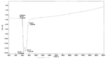
なお、本発明の接合部材の融点は、Sn-Bi-In合金部分の融点である。またその測定方法は、後述する実施例に記載のように、DSCで測定したときの吸熱ピークのトップ温度をその成分の融点として扱うものである。また、ピークが複数ある場合は、最も低い温度の吸熱ピークを最低融点とし、最も高い温度の吸熱ピークを最高融点として扱う。
By setting the Sn-Bi-In composition within the composition range of the joining member of the present invention described above, the melting point of the solder alloy can be stably set to 69 to 110 ° C, and at 90 to 135 ° C in the low temperature region. It is characterized by being suitable for low temperature mounting because it can be joined by heating reflow. Further, it is a joining member having high joining reliability.
The melting point of the joining member of the present invention is the melting point of the Sn—Bi—In alloy portion. Further, in the measuring method, as described in Examples described later, the top temperature of the endothermic peak measured by DSC is treated as the melting point of the component. When there are a plurality of peaks, the endothermic peak at the lowest temperature is treated as the lowest melting point, and the endothermic peak at the highest temperature is treated as the highest melting point.
本発明の接合部材はIn濃度の上限を40質量%としている。これを超えるIn濃度でもSn-Bi-Inはんだ合金の融点が110℃以下となる場合があるが、In濃度が50質量%を超えると当該はんだ合金と被めっき物の接着強度が既存のPbフリーはんだ(Sn2.5Ag、Sn3.2Ag、Sn58Bi合金など)の3.3mg/μm2よりも低下してしまうため、実装用導電性接合材として使用できない場合がある。 The joining member of the present invention has an upper limit of In concentration of 40% by mass. Even if the In concentration exceeds this, the melting point of the Sn-Bi-In solder alloy may be 110 ° C or lower, but if the In concentration exceeds 50% by mass, the adhesive strength between the solder alloy and the object to be plated is Pb-free. Since it is lower than 3.3 mg / μm 2 of solder (Sn2.5Ag, Sn3.2Ag, Sn58Bi alloy, etc.), it may not be used as a conductive bonding material for mounting.
また、In濃度が40質量%を超えると当該めっき積層物および当該はんだ合金の融点が69℃未満になり、電子製品の通常の使用温度環境下における接合耐久性の低下が懸念される。また、Inは高価なため、多く用いることはコスト増となるため汎用性の観点からも好ましくない。 Further, when the In concentration exceeds 40% by mass, the melting point of the plated laminate and the solder alloy becomes less than 69 ° C., and there is a concern that the bonding durability of the electronic product under the normal operating temperature environment is lowered. Further, since In is expensive, it is not preferable from the viewpoint of versatility because using it in large quantities increases the cost.
(めっき)
本発明のSn-Bi-In系低融点接合部材等の形成については、Snめっき、Biめっき、Inめっきをそれぞれ行うことで得られる低融点めっき積層物を利用する方法であるめっき積層法を主体に説明する。めっき方法は、電解めっきまたは無電解めっきのいずれの方法でも可能であるが、めっき所要時間や生産性などを考慮すると電解めっきが好ましい。
(Plating)
The formation of the Sn-Bi-In low melting point bonding member and the like of the present invention mainly consists of a plating lamination method which is a method of utilizing a low melting point plating laminate obtained by performing Sn plating, Bi plating, and In plating, respectively. Explain to. The plating method can be either electrolytic plating or electroless plating, but electrolytic plating is preferable in consideration of the required plating time and productivity.
使用可能なめっき装置を電解めっきの場合を例に述べると、用いる各めっき液に対して耐蝕性を有する材質で構成されためっき槽に、撹拌翼、揺動、スキージ撹拌などの撹拌機能と電流値を所定の範囲で制御できる整流器を備えたものを使用して、陽極に溶解性アノードや不溶性アノードなどを用いて、陰極に被めっき物をセットできるめっき装置を用いることができる。 Taking the case of electrolytic plating as an example of a plating device that can be used, a plating tank made of a material that is corrosion resistant to each plating solution to be used has a stirring function such as stirring blades, rocking, and squeegee stirring, and current. A plating device capable of setting an object to be plated on the cathode can be used by using a rectifier capable of controlling the value within a predetermined range, using a soluble anode or an insoluble anode as the anode.
めっき積層の工程をSn→Bi→Inの順で積層する場合を例に説明すると、「被めっき物の表面洗浄・乾燥→Snめっき→水洗・乾燥→Biめっき→水洗・乾燥→Inめっき→水洗・乾燥→レジスト除去→水洗・乾燥→はんだ合金バンプ化(加熱リフロー)」の順で行われる。 To explain the case where the plating lamination process is laminated in the order of Sn → Bi → In, “Surface cleaning / drying of the object to be plated → Sn plating → water washing / drying → Bi plating → water washing / drying → In plating → water washing”・ Drying → resist removal → washing / drying → solder alloy bumping (heating reflow) ”is performed in this order.
以下に、本発明のSn-Bi-In系低融点はんだ合金およびそのはんだ合金バンプの形成について工程ごとに説明する。 Hereinafter, the formation of the Sn-Bi-In-based low melting point solder alloy of the present invention and the solder alloy bumps thereof will be described for each step.
(接合部材を配置する対象部材)
本発明にかかるSn-Bi-In系低融点はんだ合金やそのはんだ合金バンプを形成させる対象となる部材は、LSIなどの半導体電子部品またはこれを複数搭載して回路構成されたパッケージやモジュールとするためのプリント配線板などの配線基板などである。これらの部材は、必要に応じてその表面をフォトリソグラフィー等により所要の導電性接合部(パッド)がパターン形成されたものを使用する。
(Target member to place the joining member)
The Sn-Bi-In-based low melting point solder alloy according to the present invention and the member to be formed to form the solder alloy bump thereof are semiconductor electronic components such as LSI or a package or module in which a plurality thereof are mounted to form a circuit. It is a wiring board such as a printed wiring board for the purpose. As these members, those having the required conductive joints (pads) patterned on the surface thereof by photolithography or the like are used, if necessary.
また、大きさが1mm以下である、微小金属ボール、導電性の金属の被覆層を有する微小樹脂ボール、はんだ合金の被覆層を有する微小樹脂ボール、および微小ピン部材からなる群から選択されるいずれかのコア材を用いることもできる。これらのコア材の表層に、Sn-Bi-In合金を用いて被覆して本発明の接合部材とすることができる。これらのコア材の被覆は、めっきにより行ったり、はんだ合金化したSn-Bi-In合金等で被覆してもよい。 Further, any of the groups selected from the group consisting of micrometal balls having a size of 1 mm or less, microresin balls having a conductive metal coating layer, microresin balls having a solder alloy coating layer, and micropin members. The core material can also be used. The surface layer of these core materials can be coated with a Sn—Bi—In alloy to obtain the joining member of the present invention. The coating of these core materials may be performed by plating, or may be coated with a solder alloyed Sn-Bi-In alloy or the like.
コア材としてボールグリットアレイ(以下、BGAという)等の微小ボール搭載型の導電性接合材料のコアボールとして用いられる微小ボールを用いることもできる。微小ボールは、直径1mm以下の微小金属ボールまたは微小樹脂ボールを使用できる。特に微小樹脂ボールは電子回路部品の軽量化、熱応力緩和(弾性変形が可能)などに有効なコアボール材として用いられている。 As the core material, microballs used as core balls of a microball-mounted conductive joining material such as a ball grit array (hereinafter referred to as BGA) can also be used. As the minute balls, a minute metal ball or a minute resin ball having a diameter of 1 mm or less can be used. In particular, microresin balls are used as core ball materials that are effective for reducing the weight of electronic circuit parts and relaxing thermal stress (which can be elastically deformed).
微小金属ボールとしては、例えば、直径が0.05~1.0mmのCu、Ni-Co-Fe合金や、Ni-Fe合金などの導電性金属球であればいずれも用いることができる。また、必要に応じてその表面に厚み0.1~30μmのNi、Cu、はんだなどの導電性被覆を施した微小金属ボールの使用も可能である。また、微小金属ボールの変わりに円柱状の微小金属ピンを用いることもできる。 As the minute metal ball, for example, any conductive metal ball such as Cu, Ni—Co—Fe alloy or Ni—Fe alloy having a diameter of 0.05 to 1.0 mm can be used. Further, if necessary, it is also possible to use a minute metal ball having a surface thereof coated with a conductive coating such as Ni, Cu, or solder having a thickness of 0.1 to 30 μm. Further, a columnar micrometal pin can be used instead of the micrometal ball.
微小樹脂ボールとしては、例えば、直径が0.05~1.0mmのアクリル樹脂、ポリプロピレン樹脂、塩化ビニル樹脂、ポリフェニレンサルファイト、ジビニルベンゼン架橋重合体などの一般的な樹脂で微小ボール化が可能なものであればいずれも用いることができる。なお、これらの微小樹脂ボールは非導電性のため、その表面に無電解めっき等により0.5~5.0μm程度のNi、Cu、はんだなどの導電性金属または合金等で被覆したものを使用する。 As the fine resin ball, for example, a general resin such as an acrylic resin having a diameter of 0.05 to 1.0 mm, a polypropylene resin, a vinyl chloride resin, polyphenylene sulfide, and a divinylbenzene crosslinked polymer can be used to form a fine ball. Any of them can be used. Since these minute resin balls are non-conductive, those whose surface is coated with a conductive metal or alloy such as Ni, Cu, or solder of about 0.5 to 5.0 μm by electroless plating or the like is used. do.
また、コア材はボール状に限られず、円柱状や角柱状、錘状、またこれらの角を面取りした形状などの微小ピンを用いることもできる。微小ピンは、前述の微小金属ボールや微小樹脂ボールに準じる材質や大きさ等を有する微小金属ピンや微小樹脂ピンを用いることができる。なお、微小ピンの場合、最も小さい辺を、微小金属ボールや微小樹脂ボールにおける直径に相当するものとする。 Further, the core material is not limited to a ball shape, and micropins such as a columnar shape, a prismatic shape, a weight shape, and a shape in which these corners are chamfered can also be used. As the minute pin, a minute metal pin or a minute resin pin having the same material and size as the above-mentioned minute metal ball or minute resin ball can be used. In the case of a minute pin, the smallest side corresponds to the diameter of the minute metal ball or the minute resin ball.
(被めっき物の表面洗浄・乾燥)
被めっき物の表面洗浄は、被めっき物の表面の付着物を除去して清浄化することが目的であり、付着物除去が可能な溶媒を選定して用いる。例えば、有機溶媒としてはメタノール、エタノール、イソプロピルアルコール等の低級アルコール類、アセトン、メチルエチルケトン(MEK)、イソブチルケトン(MIBK)等のケトン類などが挙げられる。水系溶媒としては、アンモニア、有機アミン化合物等と過酸化水素水の併用、アニオン系、カチオン系、ノニオン系の界面活性剤などが添加された水溶液が挙げられる。これらの溶媒のうち、被めっき物の材質を侵さないことを考慮して適時選択して用いる。
(Surface cleaning and drying of the object to be plated)
The purpose of surface cleaning of the object to be plated is to remove and clean the deposits on the surface of the object to be plated, and a solvent capable of removing the deposits is selected and used. For example, examples of the organic solvent include lower alcohols such as methanol, ethanol and isopropyl alcohol, and ketones such as acetone, methyl ethyl ketone (MEK) and isobutyl ketone (MIBK). Examples of the aqueous solvent include a combined use of ammonia, an organic amine compound and the like and a hydrogen peroxide solution, and an aqueous solution to which an anionic, cationic or nonionic surfactant is added. Of these solvents, they are selected and used in a timely manner in consideration of not attacking the material of the object to be plated.
被めっき物の表面洗浄は、室温~100℃の範囲内でこれらの溶媒中に浸漬または溶媒でのシャワー洗浄などの方法で洗浄する。溶媒洗浄後は、表面に付着した溶媒成分を水洗して、表面を清浄化すれば良い。次に、被めっき物の乾燥であるが、室温~100℃の範囲で加温乾燥または通風乾燥すれば良い。なお、乾燥工程は省略して次めっき工程に進めることも可能である。 The surface of the object to be plated is washed by a method such as immersion in these solvents or shower washing with a solvent within the range of room temperature to 100 ° C. After washing with the solvent, the solvent component adhering to the surface may be washed with water to clean the surface. Next, regarding the drying of the object to be plated, heating drying or ventilation drying may be performed in the range of room temperature to 100 ° C. It is also possible to omit the drying step and proceed to the next plating step.
(アンダーメタルの形成)
導電性接合部がパターン形成された被めっき物の表面に、必要に応じてTi(チタン)、Ni(ニッケル)、Cu(銅)、Au(金、Sn(スズ)、Ag(銀)、Cr(クロム)、Pd(パラジウム)、Pt(白金)、W(タングステン)、Co(コバルト)、TiW(チタン-タングステン)、NiP(ニッケル-リン)、NiB(ニッケル-ホウ素)、NiCo(ニッケル-コバルト)、およびNiV(ニッケル-バナジウム)からなる群から選択される1以上のアンダーメタルを成膜したものを用いることも可能である。これらのアンダーメタルは、単独または複数を積層して用いても構わない。成膜方法は、蒸着、PVD、めっき法などから適応可能な方法を適時選択して用いれば良い。成膜の膜厚は、各々で0.01~10μmの範囲で適時設定すれば良い。
(Formation of under metal)
Ti (tungsten), Ni (nickel), Cu (copper), Au (gold, Sn (tin), Ag (silver), Cr (Chrome), Pd (palladium), Pt (platinum), W (tungsten), Co (cobalt), TiW (tungsten-tungsten), NiP (nickel-phosphorus), NiB (nickel-boron), NiCo (nickel-cobalt) ), And one or more undermetals formed from the group consisting of NiV (nickel-vanadium) can also be used. These undermetals may be used alone or in combination of two or more. As the film forming method, an applicable method may be appropriately selected from vapor deposition, PVD, plating method and the like. The film forming film thickness may be set in the range of 0.01 to 10 μm in a timely manner. good.
(導電性ポストの形成)
また、集積回路の微細化に伴って導電性接合材料のはんだ合金を狭い間隔(狭ピッチ)で並べることによる実装時(加熱リフロー時)のショート防止などの目的で設けられる円柱状の導電性ポストをアンダーメタル上に形成したものを用いることも可能である。円柱状のポスト材としては、Cu、Ag、Niなどの導電性金属から適時選択すれば良い。円柱状ポストの形成は、PVD、めっき法などから適応可能な方法を適時選択して用いれば良い。円柱状ポストの高さは、1~200μmの範囲が通常であり、その必要に応じて適時設定すれば良い。
(Formation of conductive post)
In addition, a columnar conductive post provided for the purpose of preventing short circuits during mounting (during heating reflow) by arranging solder alloys of conductive joining materials at narrow intervals (narrow pitch) with the miniaturization of integrated circuits. It is also possible to use the one formed on the under metal. The columnar post material may be appropriately selected from conductive metals such as Cu, Ag, and Ni. The columnar post may be formed by appropriately selecting and using an applicable method from PVD, plating method and the like. The height of the columnar post is usually in the range of 1 to 200 μm, and may be set in a timely manner as necessary.
(Sn-Bi-In系低融点めっき積層物の形成方法)
前記した導電性接合部がパターン形成されたこれらの被めっき物上に、本発明のSn-Bi-In系低融点接合部材にかかるめっき積層物を形成する方法について以下に説明する。まず、Sn、Bi、In各々のめっき処理の方法を以下に例示する。
(Method for forming Sn-Bi-In low melting point plated laminate)
A method for forming a plated laminate to be applied to the Sn-Bi-In-based low melting point bonding member of the present invention on these objects to be plated on which the above-mentioned conductive bonding portions are patterned will be described below. First, the method of plating each of Sn, Bi, and In is illustrated below.
(Snめっき)
Snめっきは、被めっき物をめっきする主たる成分としてSnを含むめっき液等を用いて行うめっき処理である。Snめっき液は、市販のものを使用すれば良く、例えば石原ケミカル社のSnめっき液などが挙げられる。めっき条件としては、例えば撹拌翼、揺動、スキージ撹拌などを用いた撹拌下で、温度5~50℃、めっき液中のSnイオン濃度1~70g/L、電流密度0.1~20.0A/dm2の範囲内で任意に設定すれば良い。Snめっき量は、設定条件下でのめっき処理時間(めっき液浸漬時間)で制御可能である。
(Sn plating)
Sn plating is a plating process performed using a plating solution or the like containing Sn as a main component for plating an object to be plated. As the Sn plating solution, a commercially available one may be used, and examples thereof include Sn plating solution manufactured by Ishihara Chemical Co., Ltd. The plating conditions are, for example, under stirring using a stirring blade, rocking, squeegee stirring, etc., a temperature of 5 to 50 ° C., a Sn ion concentration in the plating solution of 1 to 70 g / L, and a current density of 0.1 to 20.0 A. It may be set arbitrarily within the range of / dm 2 . The Sn plating amount can be controlled by the plating treatment time (plating solution immersion time) under the set conditions.
(Biめっき)
Biめっきは、被めっき物をめっきする主たる成分としてBiを含むめっき液等を用いて行うめっき処理である。Biめっき液は、市販のものを使用すれば良く、例えば石原ケミカル社のBiめっき液などが挙げられる。めっき条件としては、例えば撹拌翼、揺動、スキージ撹拌などを用いた撹拌下で、温度5~50℃、めっき液中のBiイオン濃度1~70g/L、電流密度0.1~20.0A/dm2の範囲内で任意に設定すれば良い。Biめっき量は、設定条件下でのめっき処理時間(めっき液浸漬時間)で制御可能である。
(Bi plating)
Bi plating is a plating process performed using a plating solution or the like containing Bi as a main component for plating an object to be plated. As the Bi plating solution, a commercially available one may be used, and examples thereof include Bi plating solution manufactured by Ishihara Chemical Co., Ltd. The plating conditions are, for example, under stirring using a stirring blade, rocking, squeegee stirring, etc., a temperature of 5 to 50 ° C., a Bi ion concentration in the plating solution of 1 to 70 g / L, and a current density of 0.1 to 20.0 A. It may be set arbitrarily within the range of / dm 2 . The Bi plating amount can be controlled by the plating treatment time (plating solution immersion time) under the set conditions.
(Inめっき)
Inめっきは、被めっき物をめっきする主たる成分としてInを含むめっき液等を用いて行うめっき処理である。Inめっき液は、市販のものを使用すれば良く、例えば石原ケミカル社やEEJA社のInめっき液などが挙げられる。めっき条件としては、例えば撹拌翼、揺動、スキージ撹拌などを用いた撹拌下で、温度5~50℃、めっき液中のInイオン濃度1~70g/L、電流密度0.1~20.0A/dm2の範囲内で任意に設定すれば良い。Inめっき量は、設定条件下でのめっき処理時間(めっき液浸漬時間)で制御可能である。
(In plating)
In plating is a plating process performed using a plating solution or the like containing In as a main component for plating an object to be plated. As the In plating solution, a commercially available one may be used, and examples thereof include In plating solutions manufactured by Ishihara Chemical Co., Ltd. and EEJA Co., Ltd. The plating conditions are, for example, under stirring using a stirring blade, rocking, squeegee stirring, etc., a temperature of 5 to 50 ° C., an In ion concentration of 1 to 70 g / L in the plating solution, and a current density of 0.1 to 20.0 A. It may be set arbitrarily within the range of / dm 2 . The amount of In plating can be controlled by the plating treatment time (plating solution immersion time) under the set conditions.
なお、これらのSnめっき、Biめっき、およびInめっきは、任意で用いる混合成分等の他のめっき成分を含むものを用いてもよい。めっき液等のめっき用組成物において、主たる成分に対して他のめっき成分の総量(「他のめっき成分の総量(g/L)」/「主たる成分(g/L)」)は、50質量%以下が好ましく、30質量%以下が好ましく、20質量%以下が好ましい。例えば、Snめっきに、任意の混合成分であるCuを混合したSn・Cu混合めっき液や、Agを混合したSn・Agめっき液を、主成分としてSnを含むことからSnめっきとして用いてもよい。Biめっき、Inめっきも同様である。 As these Sn plating, Bi plating, and In plating, those containing other plating components such as an optional mixed component may be used. In a plating composition such as a plating solution, the total amount of other plating components (“total amount of other plating components (g / L)” / “main component (g / L)”) with respect to the main component is 50 mass. % Or less is preferable, 30% by mass or less is preferable, and 20% by mass or less is preferable. For example, a Sn / Cu mixed plating solution in which Cu, which is an arbitrary mixed component, or a Sn / Ag plating solution in which Ag is mixed may be used for Sn plating because it contains Sn as a main component. .. The same applies to Bi plating and In plating.
(めっき積層順番)
めっき積層順番は、SnめっきとBiめっきとInめっきを、いずれも行うものとすることができ、その順序は任意でよい。具体的には、被めっき物の表面から順に、Sn→Bi→In、Sn→In→Bi、Bi→Sn→In、Bi→In→Sn、In→Sn→Bi、In→Bi→Snの順のいずれの順番でも可能である。電解めっきでSn-Bi-Inを所定の組成で安定的に積層するには、標準電極電位が高くイオン化傾向の小さいものからめっきした方が好ましく「Bi→Sn→In」または「Sn→Bi→In」の順番で積層めっきすることがより好ましい。なお、25℃、105パスカル(Pa)で標準水素電極を基準した場合の標準電極電位は、Bi=0.317V、Sn=-0.138V、In=-0.338Vであり、3成分のなかで最も電位の低いInめっきを1つ目や2つ目のめっきとすると、Inは次成分のめっき操作中に電解めっき浴中でイオン化して溶出し易いため、めっき積層物中における濃度が設定条件よりも低下し易い。よって、Inめっきは、SnめっきおよびBiめっきを行った後に行う、最後のめっきとすることが好ましい。
(Plating stacking order)
The plating stacking order may be Sn plating, Bi plating, or In plating, and the order may be arbitrary. Specifically, in order from the surface of the object to be plated, Sn → Bi → In, Sn → In → Bi, Bi → Sn → In, Bi → In → Sn, In → Sn → Bi, In → Bi → Sn. Any order is possible. In order to stably laminate Sn-Bi-In with a predetermined composition by electrolytic plating, it is preferable to plate from the one having the highest standard electrode potential and the lowest ionization tendency, "Bi → Sn → In" or "Sn → Bi →". It is more preferable to perform laminated plating in the order of "In". When the standard hydrogen electrode is used as a reference at 25 ° C. and 105 pascal (Pa), the standard electrode potentials are Bi = 0.317V, Sn = −0.138V, and In = −0.338V, and the three components are If the In plating with the lowest potential is the first or second plating, In is easily ionized and eluted in the electrolytic plating bath during the plating operation of the next component, so that the concentration in the plated laminate is high. It tends to be lower than the set condition. Therefore, it is preferable that the In plating is the final plating performed after the Sn plating and the Bi plating.
(めっき積層物)
めっき積層物は、Sn、Bi、In各成分を単独で逐次にめっき処理して積層したものである。本発明のめっき積層物は、Sn、Bi、Inの濃度差が異なる複数の層を有している。この層は、例えば、Snめっきによる層にInが拡散したSnIn層や、Biめっきによる層にInが拡散したBiIn層を有するものとすることができる。めっき後に、これらの合金層を形成することで、Sn、Bi、In各々単独の融点よりも大幅に低い69~110℃の低融点めっき積層物にできる。
(Plated laminate)
The plated laminate is obtained by sequentially plating the Sn, Bi, and In components independently and laminating them. The plated laminate of the present invention has a plurality of layers having different concentrations of Sn, Bi, and In. This layer may have, for example, a SnIn layer in which In is diffused in a layer by Sn plating, or a BiIn layer in which In is diffused in a layer by Bi plating. By forming these alloy layers after plating, a low melting point plated laminate having a melting point of 69 to 110 ° C., which is significantly lower than the melting points of Sn, Bi, and In alone, can be obtained.
なお、めっき積層物における各元素の濃度は、めっき積層物を被めっき物から剥離して、酸溶解後、高周波誘導結合プラズマ-発光分析装置によって定量分析して、その濃度を求めることができる。各層は、その層の主たる金属となるSnやBi、Inを含み、SnIn層はSnとInを含み、BiIn層はBiとInを含む。 The concentration of each element in the plated laminate can be determined by peeling the plated laminate from the object to be plated, dissolving the acid, and then quantitatively analyzing it with a high-frequency inductively coupled plasma-emission analyzer. Each layer contains Sn, Bi, and In, which are the main metals of the layer, the SnIn layer contains Sn and In, and the BiIn layer contains Bi and In.
各層は、実質的にその層を構成する金属元素からなるものであることが好ましいが、その層の金属元素に加えて、原料や製造工程上、不可避的に含まれる不純物を含むものでもよい。このような不純物としては、Fe(鉄)やC(炭素)などがあげられる。 Each layer is preferably composed of a metal element substantially constituting the layer, but may contain impurities inevitably contained in a raw material or a manufacturing process in addition to the metal element of the layer. Examples of such impurities include Fe (iron) and C (carbon).
また、後述するような混合元素として含まれる任意添加元素を含むものとしてもよい。なお、Pbフリーとして使用するためにPbの混合量を低減することが好ましく、Sn-Bi-In合金におけるPbの濃度は0.1質量%以下が好ましく、0.05質量%以下、0.01質量%以下がより好ましい。Pbは検出下限以下であることがさらに好ましい。 Further, it may contain an optional additive element contained as a mixed element as described later. In addition, it is preferable to reduce the mixing amount of Pb for use as Pb-free, and the concentration of Pb in the Sn—Bi—In alloy is preferably 0.1% by mass or less, 0.05% by mass or less, 0.01. More preferably, it is by mass or less. It is more preferable that Pb is not less than the lower limit of detection.
接合部材において、Sn-Bi-Inの三元状態図における濃度は、めっき積層物やはんだ合金といったSn-Bi-In合金の部分における、Sn、Bi、およびIn各々のめっき成分元素の合計を100質量%としたときの各元素が占める割合(質量分率)により規定したものである。また、めっき積層物やはんだ合金といったSn-Bi-In合金の部分において、Sn、Bi、およびInの合計量が占める割合(Sn+Bi+Inの質量/Sn-Bi-In合金の全質量)は、70質量%以上が好ましく、80質量%以上がより好ましく、90質量%以上であることがさらに好ましく、95質量%以上が特に好ましい。 In the joining member, the concentration in the ternary state diagram of Sn-Bi-In is 100, which is the total of the plating component elements of Sn, Bi, and In in the portion of the Sn-Bi-In alloy such as the plated laminate and the solder alloy. It is defined by the ratio (mass fraction) occupied by each element when it is defined as% by mass. Further, the ratio of the total amount of Sn, Bi, and In in the portion of the Sn—Bi—In alloy such as the plated laminate or the solder alloy (mass of Sn + Bi + In / total mass of Sn—Bi—In alloy) is 70 mass. % Or more is preferable, 80% by mass or more is more preferable, 90% by mass or more is further preferable, and 95% by mass or more is particularly preferable.
(Snの層)
Snめっきにより得られるSnの層は、Sn(スズ)を含む層である。Snの層は、Inを除いてSnを主たる成分として含んでおり、この層におけるInを除く元素におけるSn濃度は、70質量%以上が好ましく、80質量%以上がより好ましく、90質量%以上であることがさらに好ましい。このSnの層は、Snめっきにより得ることができる。
(Sn layer)
The Sn layer obtained by Sn plating is a layer containing Sn (tin). The Sn layer contains Sn as a main component excluding In, and the Sn concentration in the elements excluding In in this layer is preferably 70% by mass or more, more preferably 80% by mass or more, and 90% by mass or more. It is more preferable to have. This Sn layer can be obtained by Sn plating.
また、Snの層は、Inも含む、SnIn層としてもよい。このSnIn層は、その層の主たる成分として、SnおよびInを含み、SnとInの合計が、その層における70質量%以上や、80質量%以上、90質量%以上、95質量%以上とすることができる。SnIn層は、双方を含み、Sn:Inの質量比率が、1:99~99:1であり、5:95~95:5や、10:90~90:10、20:80~80:20などとすることもできる。 Further, the Sn layer may be a SnIn layer including In. This SnIn layer contains Sn and In as the main components of the layer, and the total of Sn and In is 70% by mass or more, 80% by mass or more, 90% by mass or more, and 95% by mass or more in the layer. be able to. The SnIn layer contains both, and the mass ratio of Sn: In is 1:99 to 99: 1, 5:95 to 95: 5, 10:90 to 90:10, 20:80 to 80:20. And so on.
(Biの層)
Biめっきにより得られるBiの層は、Bi(ビスマス)を含む層である。Biの層は、Inを除いてBiを主たる成分として含んでおり、この層におけるInを除く元素におけるBi濃度は、70質量%以上が好ましく、80質量%以上がより好ましく、90質量%以上であることがさらに好ましい。このBiの層は、Biめっきにより得ることができる。
(Bi layer)
The Bi layer obtained by Bi plating is a layer containing Bi (bismuth). The Bi layer contains Bi as a main component excluding In, and the Bi concentration in the element excluding In in this layer is preferably 70% by mass or more, more preferably 80% by mass or more, and 90% by mass or more. It is more preferable to have. This Bi layer can be obtained by Bi plating.
また、Biの層は、Inも含む、BiIn層としてもよい。このBiIn層は、その層の主たる成分として、BiおよびInを含み、BiとInの合計が、その層における70質量%以上や、80質量%以上、90質量%以上、95質量%以上とすることができる。BiIn層は、双方を含み、Bi:Inの質量比率が、1:99~99:1であり、5:95~95:5や、10:90~90:10、20:80~80:20などとすることもできる。 Further, the Bi layer may be a BiIn layer including In. This BiIn layer contains Bi and In as the main components of the layer, and the total of Bi and In is 70% by mass or more, 80% by mass or more, 90% by mass or more, and 95% by mass or more in the layer. be able to. The BiIn layer contains both, and the mass ratio of Bi: In is 1:99 to 99: 1, 5:95 to 95: 5, 10:90 to 90:10, 20:80 to 80:20. And so on.
(Inの層)
Inめっきにより積層めっき層に含まれるInは、めっき処理中にSnの層やBiの層中に拡散し易いため、In単独を主成分とした単独層は形成し難く、SnIn合金またはBiIn合金の形態で形成される場合がある。
(In layer)
Since In contained in the laminated plating layer by In plating easily diffuses into the Sn layer and the Bi layer during the plating process, it is difficult to form a single layer containing In alone as a main component, and it is difficult to form a single layer containing In alone. May be formed in morphology.
(めっき積層数)
積層めっき層のめっき積層数は、特に限定されず、Sn、Bi、Inの濃度が異なる2層以上の複数の層を有するものであれば良い。なお、被めっき物とめっき成分の相互作用による双方成分の合金化や拡散防止などの目的により、前記の3成分の濃度が異なる層を形成させて、3層や、4層、5層などの積層も可能である。
(Number of plated layers)
The number of plated layers of the laminated plating layer is not particularly limited, and may be any one having two or more layers having different concentrations of Sn, Bi, and In. For the purpose of alloying both components and preventing diffusion due to the interaction between the object to be plated and the plating components, layers having different concentrations of the above three components are formed to form three layers, four layers, five layers, or the like. Laminating is also possible.
(各めっき工程後の水洗・乾燥)
各めっき工程後の水洗の目的は、めっき浴から引上げた時に被めっき物の表面に付着しためっき液の除去であり、水中に浸漬または水シャワーにより水洗して清浄化する。その後の乾燥は、めっき積層物の融点未満の温度で乾燥すれば良い。めっき積層物の融点を考慮したうえで、通常は室温~100℃の範囲で適時設定して加温乾燥または通風乾燥すれば良い。なお、次工程で残存水分があっても問題なければ、乾燥工程を省略して次工程に進めることも可能である。
(Washing and drying after each plating process)
The purpose of washing with water after each plating step is to remove the plating solution adhering to the surface of the object to be plated when it is pulled up from the plating bath, and it is cleaned by immersing it in water or washing it with water by a water shower. Subsequent drying may be performed at a temperature lower than the melting point of the plated laminate. In consideration of the melting point of the plated laminate, usually, it may be set appropriately in the range of room temperature to 100 ° C. and then heated and dried or ventilated. If there is no problem even if there is residual water in the next step, it is possible to skip the drying step and proceed to the next step.
(パターン用レジストの除去)
レジストパターン除去は、Sn-Bi-In系低融点めっき積層物を侵さずにレジスト除去できる薬液に浸漬またはシャワー洗浄などの公知の湿式法、または酸素プラズマによるアッシング処理などの方法を用いて除去することが可能である。
(Removal of resist for pattern)
The resist pattern is removed by using a known wet method such as immersion in a chemical solution capable of removing the resist without damaging the Sn-Bi-In low melting point plating laminate or shower washing, or a method such as ashing treatment with oxygen plasma. It is possible.
湿式法の場合に用いる薬液としては、例えば、主成分がジメチルスルホキシドなどの有機溶媒、水酸化カリウムなどの水系溶媒などが挙げられ、レジスト材料の除去性やめっき析出物の耐性を考慮して適時選択すれば良い。薬液でのレジスト除去後に、被めっき物を水中に浸漬または水シャワーにより水洗して清浄化した後、室温~100℃の範囲で加温乾燥または通風乾燥する。 Examples of the chemical solution used in the wet method include an organic solvent whose main component is dimethyl sulfoxide and the like, an aqueous solvent such as potassium hydroxide, and the like, and timely considering the removability of the resist material and the resistance of the plating precipitate. Just choose. After removing the resist with a chemical solution, the object to be plated is immersed in water or washed with water in a water shower to clean it, and then heated and dried or ventilated and dried in the range of room temperature to 100 ° C.
(微量金属の添加)
本発明のSn-Bi-In系低融点接合部材は、皮膜の平滑性や、密着性などの物性向上の目的で、融点が110℃を超えない範囲で、適宜、Sn-Bi-In合金に、Ag、Cu、Ni、Zn、およびSbからなる群から選択される1以上の混合成分を含み、Sn-Bi-In合金における前記混合成分の合計質量が占める割合(混合成分の合計質量/Sn-Bi-In合金の質量)が、0.001~3.0質量%の範囲で混合することも可能である。これらの特定の混合成分の混合の方法は、合金成分を調整するとき混合する金属を所定量含んだ状態で合金化させることができる。例えば、Sn-Bi-In系低融点めっき積層物を用いる場合、含有量が所定量になる様に、Sn、Bi、Inのいずれかのめっき液中に添加して被膜中に導入すれば良い。
(Addition of trace metal)
The Sn-Bi-In low melting point bonding member of the present invention is appropriately made into a Sn-Bi-In alloy within a range where the melting point does not exceed 110 ° C. for the purpose of improving physical properties such as film smoothness and adhesion. , Ag, Cu, Ni, Zn, and Sb containing one or more mixed components selected from the group, and the ratio of the total mass of the mixed components in the Sn—Bi—In alloy (total mass of mixed components / Sn). -The mass of the Bi-In alloy) can be mixed in the range of 0.001 to 3.0% by mass. The method of mixing these specific mixed components can be alloyed with a predetermined amount of metal to be mixed when the alloy components are prepared. For example, when a Sn-Bi-In low melting point plating laminate is used, it may be added to any of Sn, Bi, and In plating solutions and introduced into the coating film so that the content becomes a predetermined amount. ..
なお、錯化剤等により、析出電位を調整して添加金属との合金めっきを得る観点からSnめっき液中またはBiめっき液中に添加することが好ましい。SnまたはBiめっき液中へのこれらの添加金属の添加量は、SnまたはBiの質量濃度に対して1/1000~1/10濃度の範囲で、得られるめっき積層物中で所定濃度になる様に適時選定して用いれば良い。 From the viewpoint of adjusting the precipitation potential with a complexing agent or the like to obtain alloy plating with the added metal, it is preferable to add it in the Sn plating solution or the Bi plating solution. The amount of these added metals added to the Sn or Bi plating solution is in the range of 1/1000 to 1/10 of the mass concentration of Sn or Bi so that the concentration becomes a predetermined concentration in the obtained plating laminate. It may be selected and used in a timely manner.
以上のように得られたSn-Bi-In系低融点接合部材は、融点が69~110℃と低融点のため、これを90~135℃の低温領域で加熱リフローして用いることができる。この接合部材は、めっき積層物の状態のまま実装工程で用いても良いし、後述する低融点はんだ合金バンプ化して実装工程で用いても良い。 Since the Sn-Bi-In-based low melting point bonding member obtained as described above has a low melting point of 69 to 110 ° C., it can be used by heating and reflowing in a low temperature region of 90 to 135 ° C. This joining member may be used in the mounting process as it is in the state of the plated laminate, or may be formed into a low melting point solder alloy bump, which will be described later, and used in the mounting process.
また、導電性接合材料として用いるはんだ合金の製造方法は、各々の合金成分を粉砕または破砕し、表面洗浄・乾燥して所定の組成になる様に配合混合したものを、配合成分中で最も高い成分の融点以上で加熱溶融して合金化したものを塊状で取り出し、更にこれを粉砕して合金微粒子とし、フラックス成分などと調合してはんだ合金ペースト等にしたものを被めっき物に塗布して加熱リフローにより実装するものがあげられる。本発明のはんだ合金もこの製造方法で製造してもよい。この方法は、工程が多く生産性が低下し、集積回路の微細化に伴う配線接合の狭ピッチ化に伴う寸法信頼性への適応が難しい場合がある。 In addition, the method for manufacturing a solder alloy used as a conductive bonding material is the highest among the compounding components, in which each alloy component is crushed or crushed, surface-cleaned and dried to obtain a predetermined composition. The alloyed material that is heated and melted above the melting point of the component is taken out as a lump, which is further crushed into alloy fine particles, which is mixed with a flux component to form a solder alloy paste, etc., and applied to the object to be plated. Some are mounted by heating reflow. The solder alloy of the present invention may also be manufactured by this manufacturing method. This method has many steps and the productivity is lowered, and it may be difficult to adapt to the dimensional reliability due to the narrowing of the pitch of the wiring connection due to the miniaturization of the integrated circuit.
Sn-Bi-In系低融点めっき積層物を加熱リフローしてはんだ合金化する方法は、これらの工程を大幅に軽減し、かつ微細なパターン形成表面に直接、めっき工法で導電性接合材料を形成するため寸法信頼性が高いことおよび得られるSn-Bi-In系はんだ合金が69~110℃の低融点であるため、90~135℃の低温領域での加熱リフローによる接合が可能であり、低温実装に適している。このような観点から、はんだ合金は、被めっき物の表面に設けられたSnめっき、Biめっき、およびInめっきを行い得られる積層めっき層を有するものを用いることが好ましい。 The method of heating and reflowing the Sn-Bi-In low melting point plating laminate to form a solder alloy significantly reduces these steps and forms a conductive bonding material directly on the fine pattern forming surface by the plating method. Therefore, since the dimensional reliability is high and the obtained Sn—Bi-In solder alloy has a low melting point of 69 to 110 ° C., it is possible to join by heating reflow in a low temperature region of 90 to 135 ° C., and the temperature is low. Suitable for mounting. From such a viewpoint, it is preferable to use a solder alloy having a laminated plating layer that can be subjected to Sn plating, Bi plating, and In plating provided on the surface of the object to be plated.
(はんだ合金バンプの形成)
本発明の接合部材は、はんだ合金の形態とすることもできる。このはんだ合金バンプを製造するにあたっては、Sn-Bi-In系低融点接合部材に係るめっき積層物を90~135℃の低温領域で加熱リフロー処理してバンプ形成したものを用いてもよい。一般的に加熱リフローによるはんだ合金バンプの形成では、合金組成が均一で表面凹凸が無く、均一な球状または半球状の形状物性が求められる。また、実装物性としては、被めっき物などの接合部材の接着対象物との接合強度が3.3mg/μm2以上、ヒートサイクル耐久性などが必要である。これらの要求物性に悪影響する因子は、はんだ合金そのものの基本物性や、加熱リフロー前の合金成分の自然酸化膜や不純物付着や混入などがあげられる。
(Formation of solder alloy bumps)
The joining member of the present invention may also be in the form of a solder alloy. In manufacturing this solder alloy bump, a plated laminate related to a Sn—Bi—In low melting point bonding member may be heated and reflowed in a low temperature region of 90 to 135 ° C. to form a bump. Generally, in the formation of solder alloy bumps by heating reflow, it is required that the alloy composition is uniform, there is no surface unevenness, and uniform spherical or hemispherical shape physical properties are required. Further, as the mounting physical characteristics, it is necessary that the bonding strength of the bonding member such as the object to be plated with the object to be bonded is 3.3 mg / μm 2 or more, and the heat cycle durability is required. Factors that adversely affect these required physical properties include the basic physical properties of the solder alloy itself, the natural oxide film of the alloy component before heating reflow, and the adhesion and mixing of impurities.
Sn-Bi-In系低融点めっき積層物のはんだ合金バンプ化では、加熱リフロー時の低温での自然酸化膜除去を目的に「ぎ酸ガス還元法」を用いる。自然酸化膜の除去方法としては、一般的には以下に示す「ぎ酸ガス還元法」と「水素ガス還元法」があり、後者は230℃以上で、前者は150℃付近で還元反応が生じるため、低温処理、安全性、信頼性、コスト面で優位な「ぎ酸ガス還元法」の適応が好ましい。
・ぎ酸ガス還元法 MeO + HCOOH → Me + CO2 +H2O
・水素ガス還元法 MeO + H2 → Me + H2O
In the solder alloy bump formation of the Sn-Bi-In low melting point plating laminate, the "silicic acid gas reduction method" is used for the purpose of removing the natural oxide film at a low temperature during heating reflow. As a method for removing the natural oxide film, there are generally the "geic acid gas reduction method" and the "hydrogen gas reduction method" shown below. The latter causes a reduction reaction at 230 ° C or higher, and the former causes a reduction reaction at around 150 ° C. Therefore, it is preferable to apply the "hydrogen gas reduction method", which is superior in terms of low temperature treatment, safety, reliability, and cost.
・ Formic acid gas reduction method MeO + HCOOH → Me + CO 2 + H 2 O
・ Hydrogen gas reduction method MeO + H 2 → Me + H 2 O
Sn-Bi-In系低融点めっき積層物の加熱リフローは、「ぎ酸ガス還元法」を用いて、還元剤:ぎ酸、圧力:20~400mbar、昇温速度:10~150℃/min、トップ温度:70~110℃、トップ温度保持時間:20~300秒の範囲で、Sn-Bi-In系低融点めっき積層物の組成見合いで適時選定すれば良い。こうして得られる本発明のSn-Bi-In系低融点接合部材は、実装時の加熱リフロー温度が90~135℃の低温領域での接合が可能であるため低温実装に適することが特徴である。 The heating reflow of the Sn-Bi-In low melting point plated laminate uses the "silic acid gas reduction method", reducing agent: formic acid, pressure: 20 to 400 mbar, temperature rising rate: 10 to 150 ° C./min, The top temperature may be selected in the range of 70 to 110 ° C. and the top temperature holding time: 20 to 300 seconds in a timely manner according to the composition of the Sn-Bi-In low melting point plated laminate. The Sn-Bi-In-based low-melting point bonding member of the present invention thus obtained is characterized in that it is suitable for low-temperature mounting because it can be bonded in a low temperature region where the heating reflow temperature at the time of mounting is 90 to 135 ° C.
(コア材へのめっき積層)
次に、被めっき物等としてBGA等の微小ボール搭載型の導電性接合材料のコアボールとして用いられる微小金属ボールおよび微小樹脂ボール、微小ピンなどのコア材の表層が、Sn-Bi-In系低融点めっき積層物で被覆された接合部材を形成する方法について説明する。
(Plating and laminating on core material)
Next, the surface layer of the core material such as a minute metal ball, a minute resin ball, and a minute pin used as a core ball of a conductive bonding material mounted on a minute ball such as BGA as an object to be plated is a Sn-Bi-In system. A method for forming a joining member coated with a low melting point plating laminate will be described.
(微小金属ボールなどへのめっき積層)
微小金属ボールなどのコア材のめっき方法としては、円周方向に回転する円柱状めっき槽で、めっき槽内中央部に陽極、槽内円周部に陰極が配設され、回転軸が水平軸による垂直方向回転あるいは傾斜軸による傾斜回転し、5~200rpm程度の回転数でめっき処理を行う。具体的には、槽内にめっき液と被めっき物のボール等を入れて、所定のめっき厚みになる様に電流密度および通電時間を設定してめっき処理を行い、終了すれば回転円周部よりめっき処理されたボール等およびめっき液が排出される回転型めっき装置(バレルめっき法)を用いることができる。また、これを微小金属ボールのめっき用に改良された特開平10-18096号公報や、特開平10-270836号公報に記載の回転型めっき装置や、更には特開平11-92994号公報に記載の回転型めっき装置を用いることができる。
(Plating and laminating on minute metal balls, etc.)
As a method for plating core materials such as minute metal balls, a columnar plating tank that rotates in the circumferential direction has an anode in the center of the plating tank and a cathode in the circumference of the tank, and the axis of rotation is the horizontal axis. The plating process is performed at a rotation speed of about 5 to 200 rpm by rotating in the vertical direction or tilting by the tilting axis. Specifically, a plating solution and a ball of an object to be plated are put in a tank, the current density and the energization time are set so as to have a predetermined plating thickness, and the plating process is performed. A rotary plating device (barrel plating method) in which a more plated ball or the like and a plating solution are discharged can be used. Further, the rotary plating apparatus described in JP-A-10-18096, JP-A-10-270863, which has been improved for plating fine metal balls, and further, JP-A-11-92294. Rotary plating equipment can be used.
微小金属ボール表面などにSn-Bi-In系低融点めっき積層物を形成する場合は、前記したバレルめっき法(回転型めっき装置)等の公知の装置を用いることができる。Sn、Bi、In各々のめっき方法は前述のSn-Bi-In系低融点めっき積層物の形成方法と同様の条件でめっきすれば良く、めっき積層の順番は特に限定されないが、最初(最下層)にSnめっきまたはBiめっき、最後(最上層)にInめっきすることが好ましい。また、めっき膜の平滑性、密着性向上、またはめっき処理中のボール相互の凝集防止などの物性向上の目的で前述した(特定の微量金属添加)と同様の微量金属を添加することができる。
なお、コア材として微小金属ピンなどを用いる場合も前記した微小金属ボールを用いる場合と同様に、本発明のSn-Bi-In系低融点めっき積層物を形成することが可能である
When forming a Sn-Bi-In-based low melting point plating laminate on the surface of a minute metal ball or the like, a known device such as the barrel plating method (rotary plating device) described above can be used. Each of the Sn, Bi, and In plating methods may be plated under the same conditions as the above-mentioned method for forming the Sn-Bi-In low melting point plating laminate, and the order of the plating laminates is not particularly limited, but the first (bottom layer). ) Is preferably Sn-plated or Bi-plated, and the last (top layer) is preferably In-plated. Further, the same trace metal as described above (addition of a specific trace metal) can be added for the purpose of improving the smoothness and adhesion of the plating film, or improving the physical properties such as preventing the balls from aggregating with each other during the plating process.
When a fine metal pin or the like is used as the core material, it is possible to form the Sn-Bi-In-based low melting point plating laminate of the present invention in the same manner as when the fine metal ball is used.
(微小樹脂ボールなどへのめっき積層)
微小金属ボールなどの表面にSn-Bi-In系低融点めっき積層物を被覆する方法は、前記したバレルめっき法(回転型めっき装置)等の公知の装置を用いることができる。Sn、Bi、In各々のめっき方法は前述のSn-Bi-In系低融点めっき積層物の形成方法と同様の条件でめっきすれば良く、めっき積層の順番は特に限定されないが、最初(最下層)にSnまたはBiめっき、最後(最上層)にInめっきすることが好ましい。また、めっき膜の平滑性、密着性向上、またはめっき処理中のボール相互の凝集防止などの物性向上の目的で前述した(特定の微量金属添加)と同様の微量金属を添加することができる。
(Plating and laminating on minute resin balls, etc.)
As a method of coating the surface of a fine metal ball or the like with a Sn-Bi-In low melting point plating laminate, a known device such as the barrel plating method (rotary plating device) described above can be used. Each of the Sn, Bi, and In plating methods may be plated under the same conditions as the above-mentioned method for forming the Sn-Bi-In low melting point plating laminate, and the order of the plating laminates is not particularly limited, but the first (bottom layer). ) Is Sn or Bi plated, and the last (top layer) is In plated. Further, the same trace metal as described above (addition of a specific trace metal) can be added for the purpose of improving the smoothness and adhesion of the plating film, or improving the physical properties such as preventing the balls from aggregating with each other during the plating process.
以上が、微小金属ボールや微小樹脂ボール、微小ピン部材などの表面が本発明に係るSn-Bi-In系低融点めっき積層物で被覆された接合部材を形成する方法であり、こうして得られる微小部材の接合部材は、表層の積層めっき層の融点が69~110℃の低温領域であり、そのまま実装工程で用いても良い。また、これを後述する微小ボールなどの微小部材搭載型の低融点はんだ合金バンプとして実装工程で用いても良い。 The above is a method for forming a joining member in which the surface of a minute metal ball, a minute resin ball, a minute pin member, or the like is covered with the Sn-Bi-In-based low melting point plating laminate according to the present invention, and the minute amount thus obtained. The joining member of the member has a melting point of 69 to 110 ° C. in the low temperature region of the laminated plating layer of the surface layer, and may be used as it is in the mounting step. Further, this may be used in the mounting process as a low melting point solder alloy bump mounted on a minute member such as a minute ball described later.
(微小部材搭載バンプの形成)
前記のコア材の表面をSn-Bi-In系低融点めっき積層物で被覆された微小金属ボールや微小樹脂ボールなどのバンプ形成について例示する。BGA用プリント配線板などの導電性接合部のパット上にフラックスを塗布し、その上に前記したSn-Bi-In系低融点めっき積層物で被覆された微小金属ボールや微小樹脂ボールなどを実装した後、前述のSn-Bi-In系低融点はんだ合金バンプの形成と同様の方法で加熱リフローすることで、導電性接合部のパッド上にバンプ形成が可能である。
(Formation of bumps for mounting micro members)
The formation of bumps such as micrometal balls and microresin balls in which the surface of the core material is coated with a Sn-Bi-In low melting point plating laminate will be exemplified. Flux is applied on the pad of the conductive joint such as the printed wiring board for BGA, and the fine metal balls and fine resin balls coated with the above-mentioned Sn-Bi-In low melting point plating laminate are mounted on it. After that, the bumps can be formed on the pad of the conductive joint portion by heating and reflowing in the same manner as the formation of the Sn—Bi—In type low melting point solder alloy bump described above.
(電子回路の実装)
本発明にかかるめっき積層物や、本発明にかかるめっき積層物を加熱リフローして形成されるSn-Bi-In系低融点はんだ合金バンプのような接合部材を、配線基板と、半導体チップ表面との間に配置して、90~135℃の範囲内で加熱リフローして前記配線基板と前記半導体チップとを接合する半導体電子回路の実装を行うことができる。
(Implementation of electronic circuit)
A bonding member such as a plated laminate according to the present invention or a Sn-Bi-In-based low melting point solder alloy bump formed by heating and reflowing the plated laminate according to the present invention is provided on a wiring board and a semiconductor chip surface. It is possible to mount a semiconductor electronic circuit that joins the wiring board and the semiconductor chip by arranging between the two and heating and reflowing within the range of 90 to 135 ° C.
この実装は、例えば、接合部となるはんだ合金をバンプやめっき積層物として形成した半導体チップを準備し、配線基板の接続用の電極部に重ねて、ギ酸などの還元雰囲気中で90~135℃の範囲内で加熱リフローして両者を接合する。バンプやめっき積層物は、配線基板側に形成しても良く、その場合、半導体チップ側に接続用の電極部に接合する。さらには、バンプやめっき積層物は、半導体チップ側、配線基板側ともに形成させていても良く、その場合は、バンプやめっき積層物同士を重ねて、接合する。本接合は、半導体チップや配線基板などの電子回路基板以外のはんだ付けにも適用できる。 In this mounting, for example, a semiconductor chip in which a solder alloy to be a bonding portion is formed as a bump or a plated laminate is prepared, laminated on an electrode portion for connecting a wiring board, and 90 to 135 ° C. in a reducing atmosphere such as formic acid. Heat reflow within the range of and join the two. The bumps and the plated laminate may be formed on the wiring board side, and in that case, they are joined to the electrode portion for connection on the semiconductor chip side. Further, the bumps and the plated laminates may be formed on both the semiconductor chip side and the wiring board side. In that case, the bumps and the plated laminates are overlapped and joined. This bonding can also be applied to soldering other than electronic circuit boards such as semiconductor chips and wiring boards.
なお、本発明にかかるはんだ合金バンプやめっき積層物といったSn-Bi-In合金は、所定のSn、Bi、In濃度であり、融点が低いため、135℃以下程度の加熱で溶融し、20~30℃程度の常温付近では固体である。これらのはんだ合金バンプやめっき積層物は、接合部として機能することから、これらの接合部を備え被接合物と接合するものを本願においては接合部材とよぶ。例えば、はんだ合金バンプそのものやめっき積層物そのもの、また、これらを表面等に配置させた微小部材や半導体チップ等も、本願における接合部材に含む。 The Sn-Bi-In alloys such as the solder alloy bumps and the plated laminates according to the present invention have predetermined Sn, Bi and In concentrations and have a low melting point, so that they are melted by heating at about 135 ° C. or lower and 20 to 20 to It is solid at around room temperature of about 30 ° C. Since these solder alloy bumps and plated laminates function as joints, those having these joints and joining to the object to be joined are referred to as joint members in the present application. For example, the solder alloy bump itself, the plated laminate itself, and the micromembers and semiconductor chips on which these are arranged on the surface and the like are also included in the joining member in the present application.
本発明のSn-Bi-In系低融点接合部材にかかるめっき積層物およびそのはんだ合金バンプの製造工程の概念図を図2に、その実装概念図を図3に、参考として示す。 FIG. 2 shows a conceptual diagram of the manufacturing process of the plated laminate and its solder alloy bumps on the Sn-Bi-In-based low melting point bonding member of the present invention, and FIG. 3 shows a conceptual diagram of the mounting thereof for reference.
図2は、本発明の接合部材にかかるはんだ合金バンプ形成までの製造工程の概念図の一例である。
まず、1)加工前ウエハに示すように、基板1(シリコン、化合物半導体、圧電素子、樹脂基板等)上に、パッド3(Au、Au-Cu等)が配置され、保護膜2(SiN、ポリイミド等)を有している。
次に、2)給電膜形成に示すように、保護膜2やパッド3上に、給電膜4(Ti/Cu等)を形成する。
次に、3)レジスト膜塗布に示すように、給電膜4の上に、レジスト膜5を塗布する。
次に、4)露光・現像に示すように、レジスト膜5に所定のパターンで露光・現像を行い、レジスト膜5の一部を除去する。この時、通常、パッド3に対応する位置に露光を行う。
次に、5)アンダーメタル形成に示すように、レジスト膜5を露光・現像して孔が形成された部分にアンダーメタル6(Ni、Cu等)を形成する。
次に、6)めっき積層に示すように、本発明の接合部材に関する製造方法により、積層めっき層7(Sn、Bi、In)を形成する。
次に、7)レジスト剥離に示すように、残存していたレジスト膜5も除去する。これにより、パッド3上に積層めっき層7が形成された状態となる。
次に、8)給電膜エッチングに示すように、給電膜4をエッチングにより除去する。
そして、9)バンプ形成に示すように、加熱リフローすることで、積層めっき層7から、はんだ合金バンプ8(Sn/Bi/In)が形成され、接合部材として用いることができる。なお、8)給電膜エッチング後のめっき層7をそのまま接合部材として用いることもできる。
FIG. 2 is an example of a conceptual diagram of a manufacturing process up to the formation of solder alloy bumps on the joining member of the present invention.
First, 1) as shown in the unprocessed wafer, a pad 3 (Au, Au-Cu, etc.) is arranged on a substrate 1 (silicon, compound semiconductor, piezoelectric element, resin substrate, etc.), and a protective film 2 (SiN, It has polyimide etc.).
Next, as shown in 2) Forming the feeding film, the feeding film 4 (Ti / Cu or the like) is formed on the protective film 2 and the
Next, as shown in 3) Applying the resist film, the resist
Next, as shown in 4) Exposure / development, the resist
Next, as shown in 5) Undermetal formation, the resist
Next, as shown in 6) Plating Lamination, the laminated plating layer 7 (Sn, Bi, In) is formed by the manufacturing method for the joining member of the present invention.
Next, as shown in 7) resist peeling, the remaining resist
Next, as shown in 8) Feeding film etching, the
Then, as shown in 9) Bump formation, the solder alloy bump 8 (Sn / Bi / In) is formed from the
図3は、実装の一例を示す概念図である。はんだ合金バンプ9を、対応する位置の接合用の金属膜10(Au)に接触するように配置させて(図3上部参照)、90~135℃の範囲内で加熱リフローして前記配線基板と前記半導体チップとを接合することができる(図3下部)。
FIG. 3 is a conceptual diagram showing an example of implementation. The
以下、実施例により本発明を更に詳細に説明するが、本発明は、その要旨を変更しない限り以下の実施例に限定されるものではない。 Hereinafter, the present invention will be described in more detail with reference to Examples, but the present invention is not limited to the following Examples unless the gist thereof is changed.
(めっき積層物およびはんだ合金バンプの組成測定)
実施例1~15、比較例1~9で得られたSn-Bi-In系めっき積層物をSUS基板から剥離して、酸溶解後、ICP-OES(高周波誘導結合プラズマ-発光分光分析装置)にて、定量分析を行った。また、実施例16、比較例10~13、参考例1~2については、めっき積層物を加熱リフローしたはんだ合金バンプを前記同様に測定した。使用機器及び測定条件は以下の通りである。
・測定機 Thermo Fisher Scientific社ICP発光分光分析装置 形式:iCAP6300Duo
・測定条件 検量線法による定量分析
測定波長:Sn188.9nm、Bi306.7nm、In325.6nm
(Measurement of composition of plated laminate and solder alloy bump)
The Sn-Bi-In plated laminates obtained in Examples 1 to 15 and Comparative Examples 1 to 9 were peeled off from the SUS substrate, and after acid dissolution, ICP-OES (high frequency inductively coupled plasma-emission spectroscopic analyzer). Quantitative analysis was performed at. Further, in Example 16, Comparative Examples 10 to 13, and Reference Examples 1 and 2, the solder alloy bumps obtained by heating and reflowing the plated laminate were measured in the same manner as described above. The equipment used and the measurement conditions are as follows.
-Measuring machine Thermo Fisher Scientific ICP emission spectroscopic analyzer Format: iCAP6300Duo
・ Measurement conditions Quantitative analysis by calibration curve method
Measurement wavelength: Sn188.9nm, Bi306.7nm, In325.6nm
(めっき積層物の融点測定)
実施例1~15、比較例1~9で得られたSn-Bi-In系めっき積層物をSUS基板から剥離、粉砕したサンプルを、DSC(示差走査熱量計)を用いて昇温過程における吸熱プロファイルを測定した。昇温過程のDSC測定においては、各成分の融解熱が吸熱ピークとして表れ、測定サンプルの組成によって単独または複数の吸熱ピークとなる。本発明では、便宜的に各吸熱ピークのトップ温度をその成分の融点として扱う。また、ピークが複数ある場合は、最も低い温度の吸熱ピークを最低融点、最も高い温度の吸熱ピークを最高融点とした。使用機器及び測定条件は以下の通りである。
・測定機器 セイコーインスツル株式会社DSC装置 形式:DSC6220型
・測定条件 サンプル量:10~36mg
測定パン:アルミニウム
雰囲気:窒素ガス
測定温度範囲:室温~300℃,昇温速度:10℃/分
(Measurement of melting point of plated laminate)
The Sn-Bi-In plated laminates obtained in Examples 1 to 15 and Comparative Examples 1 to 9 were peeled from the SUS substrate and crushed, and the sample was endothermic in the temperature raising process using a DSC (Differential Scanning Calorimeter). The profile was measured. In the DSC measurement in the heating process, the heat of fusion of each component appears as an endothermic peak, and it becomes one or more endothermic peaks depending on the composition of the measurement sample. In the present invention, for convenience, the top temperature of each endothermic peak is treated as the melting point of the component. When there are a plurality of peaks, the endothermic peak at the lowest temperature is defined as the lowest melting point, and the endothermic peak at the highest temperature is defined as the highest melting point. The equipment used and the measurement conditions are as follows.
・ Measuring equipment Seiko Instruments Inc. DSC equipment Type: DSC6220 type ・ Measurement conditions Sample amount: 10 to 36 mg
Measuring pan: Aluminum
Atmosphere: Nitrogen gas
Measurement temperature range: room temperature to 300 ° C, temperature rise rate: 10 ° C / min
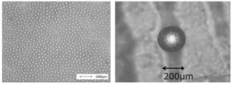
(バンプ直径の測定)
実施例16、比較例10~13、参考例1~2で得られたはんだ合金バンプのバンプ直径を画像計測にて測定した。使用機器及び測定条件は以下の通りである。
・測定機器 キーエンス社レーザー顕微鏡 形式:VK-X150
・測定条件 画像計測:200倍画像からの測長
(Measurement of bump diameter)
The bump diameters of the solder alloy bumps obtained in Example 16, Comparative Examples 10 to 13, and Reference Examples 1 and 2 were measured by image measurement. The equipment used and the measurement conditions are as follows.
・ Measuring equipment Keyence laser microscope Format: VK-X150
・ Measurement conditions Image measurement: Length measurement from 200x image
(バンプのシェア強度測定)
実施例16、比較例10~13、参考例1~2で得られたはんだ合金バンプのシェア強度をシェア強度試験機にて測定した。使用機器及び測定条件は以下の通りである。
・測定機器 DAGE社ボンドテスター 形式:4000
・測定条件 シェアスピード:150μm/s、シェア位置:はんだ部
(Measurement of bump share strength)
The share strength of the solder alloy bumps obtained in Example 16, Comparative Examples 10 to 13, and Reference Examples 1 and 2 was measured by a share strength tester. The equipment used and the measurement conditions are as follows.
・ Measuring equipment DAGE Bond Tester Format: 4000
・ Measurement conditions Share speed: 150 μm / s, Share position: Solder part
[実施例1]
脱脂洗浄したSUS304板(100mm×40mm×厚み0.3mm)の裏面の全面にテフロン(登録商標)テープを張り付け、一方の表面にテフロン(登録商標)テープを張り付けてSUS板開口部が40mm×40mmとして被めっき物とした。めっき浴としては、ガラス製1Lビーカーを用い、各々のめっき液を500mlほど入れて、陽極には白金を使用した。
Sn-Bi-In各々のめっき液は以下のものを使用した。
・Snめっき液 石原ケミカル社製(Sn濃度 5g/L)
・Biめっき液 石原ケミカル社製(Bi濃度 40g/L)
・Inめっき液 EJJA社製(In濃度 25g/L)
第1層目はBiめっきを行った。条件は、前記の被めっき物をBiめっき液に浸漬して揺動しながら、温度20℃、電流密度2A/dm2一定で、8分間めっき処理した後、引上げて、直ぐに水槽に浸漬し、これを引上げて水シャワー洗浄した。これを通風乾燥器を用いて、50℃で5分間乾燥してBiめっき物を得た。
[Example 1]
Teflon (registered trademark) tape is attached to the entire back surface of the degreased and cleaned SUS304 plate (100 mm x 40 mm x thickness 0.3 mm), and Teflon (registered trademark) tape is attached to one surface, and the SUS plate opening is 40 mm x 40 mm. As an object to be plated. A glass 1L beaker was used as the plating bath, about 500 ml of each plating solution was put therein, and platinum was used for the anode.
The following plating solutions were used for each Sn-Bi-In plating solution.
・ Sn plating solution manufactured by Ishihara Chemical Co., Ltd. (Sn concentration 5 g / L)
・ Bi plating solution manufactured by Ishihara Chemical Co., Ltd. (Bi concentration 40 g / L)
-In plating solution manufactured by EJJA (In concentration 25 g / L)
The first layer was Bi-plated. The conditions are that the object to be plated is immersed in a Bi plating solution and shaken while being plated at a temperature of 20 ° C. and a current density of 2 A / dm 2 for 8 minutes, then pulled up and immediately immersed in a water tank. I pulled it up and washed it with a water shower. This was dried at 50 ° C. for 5 minutes using a ventilation dryer to obtain a Bi-plated product.
続いて、第2層目のInめっきを行った。Biめっき処理された被めっき物をInめっき液に浸漬して揺動しながら、温度20℃、電流密度3A/dm2一定で、5分間めっき処理した後、引上げて、直ぐに水槽に浸漬し、引上げて水シャワー洗浄した。これを通風乾燥器を用いて、50℃で5分間乾燥してBi/Inめっき物を得た。
引き続いて、第3層目のSnめっきを行った。Bi-Inめっき処理された被めっき物をSnめっき液に浸漬して揺動しながら、温度20℃、電流密度1A/dm2一定で、30秒間めっき処理した後、引上げて、直ぐに水槽に浸漬し、引上げて水シャワー洗浄した。これを通風乾燥器を用いて、50℃で5分間乾燥してBi-In-Sn系のめっき積層物を得た。
得られたBi-In-Snめっき積層物をSUS板から剥ぎ取り粉砕したサンプルの組成をThermo Fisher Scientific社ICP発光分光分析装置、融点をセイコーインスツル株式会社DSC装置を用いて測定した。
Subsequently, the second layer of In plating was performed. The Bi-plated object is immersed in the In plating solution and shaken while being plated at a temperature of 20 ° C. and a current density of 3 A / dm 2 for 5 minutes, then pulled up and immediately immersed in a water tank. I pulled it up and washed it with a water shower. This was dried at 50 ° C. for 5 minutes using a ventilation dryer to obtain a Bi / In plated product.
Subsequently, Sn plating of the third layer was performed. The Bi-In plated object is immersed in the Sn plating solution and shaken while being plated at a temperature of 20 ° C. and a current density of 1 A / dm 2 for 30 seconds, then pulled up and immediately immersed in a water tank. Then, I pulled it up and washed it with a water shower. This was dried at 50 ° C. for 5 minutes using a ventilation dryer to obtain a Bi-In—Sn-based plated laminate.
The composition of the sample obtained by stripping the obtained Bi-In-Sn plated laminate from a SUS plate and pulverizing it was measured using an ICP emission spectrophotometer of Thermo Fisher Scientific Inc. and a melting point of a DSC apparatus of Seiko Instruments Inc.
[実施例2~12、比較例1~9]
実施例1と同様の方法で、めっき積層の順番と各めっき成分のめっき時間を変えて、種々のSn-Bi-In組成を振っためっき積層物サンプルを作製した。
表1に、実施例1~12および比較例1~9で得られたSn-Bi-In系めっき積層物の組成分析結果および融点測定結果を示す。また、融点測定時のDSC測定プロファイルの代表例として、実施例2、4、5、8、10、12、比較例2、4、6、8、9を図4~14に示す。なお、表1の融点判定においては、融点が69℃以上110℃以下のとき「〇」とし、69℃未満あるいは110℃を超えるものが含まれるとき「×」とした。
[Examples 2 to 12, Comparative Examples 1 to 9]
By the same method as in Example 1, the order of plating and lamination and the plating time of each plating component were changed to prepare plated laminate samples with various Sn-Bi-In compositions.
Table 1 shows the composition analysis results and melting point measurement results of the Sn-Bi-In-based plated laminates obtained in Examples 1 to 12 and Comparative Examples 1 to 9. Further, as typical examples of the DSC measurement profile at the time of melting point measurement, Examples 2, 4, 5, 8, 10, 12 and Comparative Examples 2, 4, 6, 8 and 9 are shown in FIGS. 4 to 14. In the melting point determination in Table 1, when the melting point was 69 ° C. or higher and 110 ° C. or lower, it was evaluated as “◯”, and when the melting point was less than 69 ° C. or higher than 110 ° C., it was evaluated as “x”.
被めっき物の表面に、Sn-Bi-Inを各々単独でめっき積層しためっき積層物を後述(実施例16)する様に加熱リフローしてSn-Bi-In系はんだ合金バンプを形成する本発明は、煩雑な合金製造工程が省略できると共に、めっき処理時間(めっき液浸漬時間)を変えるだけの操作でSn-Bi-In組成を任意に制御できるため、従来のはんだ合金の製造工程を著しく簡便に行うことができ、実施例1~12に示す様にSn-Bi-In組成を特定範囲内に制御することで、融点が69~110℃の当該めっき積層物が得られ、低融点領域でそのはんだ合金化が可能なことが判明した。一方、本発明のSn-Bi-In系組成範囲外である比較例1~9では、DSC測定結果からめっき積層物の融点(吸熱ピーク)が、69℃未満または110℃を超えるものが含まれることが判る。参考までに、実施例1~12、比較例1~9および後述する実施例16、比較例10~13のSn-Bi-In組成の三元状態図を図1に示す。 INDUSTRIAL APPLICABILITY The present invention forms a Sn-Bi-In-based solder alloy bump by heating and reflowing a plated laminate in which Sn-Bi-In is individually plated and laminated on the surface of the object to be plated as described later (Example 16). The complicated alloy manufacturing process can be omitted, and the Sn-Bi-In composition can be arbitrarily controlled by simply changing the plating processing time (plating liquid immersion time), which greatly simplifies the conventional solder alloy manufacturing process. By controlling the Sn—Bi-In composition within a specific range as shown in Examples 1 to 12, the plated laminate having a melting point of 69 to 110 ° C. can be obtained, and in the low melting point region. It turned out that the solder alloying is possible. On the other hand, in Comparative Examples 1 to 9 which are outside the Sn-Bi-In system composition range of the present invention, the melting point (endothermic peak) of the plated laminate is less than 69 ° C or higher than 110 ° C from the DSC measurement results. It turns out. For reference, FIG. 1 shows a ternary phase diagram of the Sn-Bi-In composition of Examples 1 to 12, Comparative Examples 1 to 9, and Examples 16 and 10 to 13 described later.
これらの結果から、Sn-Bi-In三元状態図で、Snがx質量%、Biがy質量%、Inがz質量%である点を(x、y、z)とするとき、点1(1、69、30)、点2(26、52、22)、点3(35、25、40)、点4(1、59、40)の4点を頂点とする四角形の範囲内に制御する本発明の接合部材は、融点が110℃以下のため、集積回路の低温実装の実現に大きく寄与できると判断する。また、融点が69℃以上のため、60℃程度の使用環境に曝されても耐久性を有する。
From these results, when (x, y, z) is a point where Sn is x mass%, Bi is y mass%, and In is z mass% in the Sn-Bi-In ternary state diagram,
一方、これらの範囲から外れた場合、例えば比較例1、比較例2で271℃の吸熱ピークが生じ、残留Biにより融点が高くなる。比較例3ではSn-58Bi融点近傍の136℃およびBi融点近傍の271℃に吸熱ピークが生じ、残留Sn-Bi合金および残留Biにより融点が高くなる。比較例4、比較例5では、Sn融点近傍の232℃や220℃に吸熱ピークが生じ、残留Snにより融点が高くなる。比較例6~9ではIn濃度が40質量%を超えているため、61~64℃の吸熱ピークが生じ、低融点成分による耐熱性が低下する。また、表3の比較例12、13に示すように、In濃度が50質量%を超えるとバンプシェア強度が低下する(表3)。 On the other hand, when it deviates from these ranges, an endothermic peak of 271 ° C. occurs in Comparative Example 1 and Comparative Example 2, and the melting point becomes high due to the residual Bi. In Comparative Example 3, heat absorption peaks occur at 136 ° C. near the melting point of Sn-58Bi and 271 ° C. near the melting point of Bi, and the melting point becomes higher due to the residual Sn—Bi alloy and the residual Bi. In Comparative Example 4 and Comparative Example 5, an endothermic peak occurs at 232 ° C. or 220 ° C. near the melting point of Sn, and the melting point becomes higher due to the residual Sn. In Comparative Examples 6 to 9, since the In concentration exceeds 40% by mass, an endothermic peak of 61 to 64 ° C. occurs, and the heat resistance due to the low melting point component is lowered. Further, as shown in Comparative Examples 12 and 13 in Table 3, when the In concentration exceeds 50% by mass, the bump share strength decreases (Table 3).
なお、表1(めっき積層物の組成分析と融点測定結果)に係る各組成を、三元状態図の範囲を定める点としてもよく、いずれかの点を点1~点4に代えて頂点とすることもできる。または、表1に係る点を用いて他の三角形や五角形、六角形、七角形、八角形等の多角形の頂点として範囲を定めることもできる。
In addition, each composition according to Table 1 (composition analysis and melting point measurement result of the plated laminate) may be used as a point for defining the range of the ternary phase diagram, and any point may be replaced with a

[実施例13]
Snめっき液にCuを添加した、Sn=60g/L、Cu=1g/Lのめっき液を用いて、SnCu→Bi→Inの順番でめっき積層した以外は実施例1と同様の操作を行い、微量のCu添加系めっき積層物を得た。このめっき積層物をSUS板から剥ぎ取り粉砕したサンプルの組成をThermo Fisher Scientific社ICP発光分光分析装置を用いて測定し、融点をセイコーインスツル株式会社DSC装置を用いて測定した。結果を表2(Cu、Ag微量添加系めっき積層物の組成分析と融点測定結果)に示す。
[Example 13]
The same operation as in Example 1 was performed except that the plating solution of Sn = 60 g / L and Cu = 1 g / L, in which Cu was added to the Sn plating solution, was plated and laminated in the order of SnCu → Bi → In. A trace amount of Cu-added plated laminate was obtained. The composition of the sample obtained by stripping and pulverizing this plated laminate from a SUS plate was measured using an ICP emission spectrophotometer of Thermo Fisher Scientific Inc., and the melting point was measured using a DSC device of Seiko Instruments Inc. The results are shown in Table 2 (results of composition analysis and melting point measurement of Cu and Ag trace amount addition plating laminates).
[実施例14~15]
Snめっき液にAgを添加した、Sn=40g/L、Ag=2.5g/Lのめっき液を用いて、SnAg→Bi→Inの順番でめっき積層した以外は実施例1と同様の操作を行い、微量のAg添加系めっき積層物を得た。このめっき積層物をSUS板から剥ぎ取り粉砕したサンプルの組成をThermo Fisher Scientific社ICP発光分光分析装置、融点をセイコーインスツル株式会社DSC装置を用いて測定した。結果を表2(Cu、Ag微量添加系めっき積層物の組成分析と融点測定結果)に示す。
[Examples 14 to 15]
The same operation as in Example 1 was performed except that the plating solution of Sn = 40 g / L and Ag = 2.5 g / L, in which Ag was added to the Sn plating solution, was plated and laminated in the order of SnAg → Bi → In. This was performed to obtain a trace amount of Ag-added plated laminate. The composition of the sample obtained by stripping this plated laminate from a SUS plate and pulverizing it was measured using an ICP emission spectrophotometer of Thermo Fisher Scientific Inc. and a melting point of a DSC apparatus of Seiko Instruments Inc. The results are shown in Table 2 (results of composition analysis and melting point measurement of Cu and Ag trace amount addition plating laminates).
実施例13~15の結果から、微量のCuまたはAgを添加したSn-Bi-In系めっき積層物の融点は69~107℃と低融点領域であることから、微量のCuまたはAgが添加されたSn-Bi-In系めっき積層物およびそのはんだ合金が低温実装用の導電性接合材料としての使用できることが確認された。 From the results of Examples 13 to 15, since the melting point of the Sn—Bi-In-based plated laminate to which a trace amount of Cu or Ag was added is as low as 69 to 107 ° C., a trace amount of Cu or Ag was added. It was confirmed that the Sn-Bi-In-based plated laminate and its solder alloy can be used as a conductive bonding material for low-temperature mounting.

[実施例16]
自然酸化膜付きのシリコンウェハ表面に、スパッタで厚み0.1μmのTi膜と0.3μmのCu膜を成膜し、フォトリソグラフィーにて配線接続用の開口部(60μmφ×高さ40μm:1000000個、ピッチ間隔:150μm)が設けられたレジストパターンが形成されたシリコンウェハを作製し、続いて、ポストを電解めっきでCuを10μm厚みで、更にその上に、電解めっきでNiを3μm厚みで成膜して、パターン形成被めっき物を作製した。
[Example 16]
A Ti film with a thickness of 0.1 μm and a Cu film with a thickness of 0.3 μm are formed on the surface of a silicon wafer with a natural oxide film by sputtering, and openings for wiring connection (60 μm φ x
前記のパターン形成被めっき物を用いて、実施例1と同様の方法で各めっき成分のめっき時間を変えて「Bi→Sn→In」の順番でめっき積層を行い、Sn-Bi-In系低融点めっき積層物を作製した。これを、レジスト剥離液に浸漬して、レジスト除去した後のSn-Bi-In系低融点めっき積層物の外観写真を図15に示す。更にその断面をSEM-EDX観察した結果を図16に示す。これらの図から、レジストパターン形状に相応した円柱状のめっき積層物が形成されていることが判る。また、断面SEM-EDXから、Cu/Niのアンダーメタル上にBi層→Sn層の順に積層めっきされ、InがこれらのBi層およびSn層にほぼ均一に拡散しているのが観察された。めっき積層の段階でInが下層のSn層およびBi層中に拡散して、SnInおよびBiInの合金を形成することで、最終物のめっき積層物の融点がSn、Bi、In各々単独の融点よりも大幅に低い、加熱リフロー段階でもめっき積層物全体が低融点化するものと考えられる。 Using the above-mentioned pattern-forming object to be plated, plating and laminating were performed in the order of "Bi-> Sn-> In" by changing the plating time of each plating component in the same manner as in Example 1, and the Sn-Bi-In system was low. A melting point plated laminate was prepared. FIG. 15 shows an external photograph of the Sn-Bi-In-based low melting point plating laminate after immersing this in a resist stripping solution and removing the resist. Further, the result of SEM-EDX observation of the cross section is shown in FIG. From these figures, it can be seen that a columnar plated laminate corresponding to the shape of the resist pattern is formed. Further, from the cross section SEM-EDX, it was observed that In was laminated and plated on the Cu / Ni undermetal in the order of Bi layer → Sn layer, and In was diffused almost uniformly to these Bi layer and Sn layer. In is diffused into the lower Sn layer and Bi layer at the stage of plating lamination to form an alloy of SnIn and BiIn, so that the melting point of the final plated laminate is higher than the melting point of Sn, Bi and In alone. It is considered that the melting point of the entire plated laminate is lowered even at the heating reflow stage, which is significantly lower.
続いて、このレジスト除去後のSn-Bi-In系低融点めっき積層物をシンアペックス社製VSU-200リフロー装置を用いて、下記条件でリフローしてSn-Bi-In系低融点はんだ合金バンプを作製した。このバンプ外観SEM写真を図17および図18に示す。また、そのバンプ断面をSEM-EDX観察した結果を図19に示す。バンプ外観SEM写真から、Cu/Niアンダーメタル上に半球状のはんだ合金バンプが形成されているのが判る。更に、バンプ断面のSEM-EDX写真からSn-Bi-Inがほぼ均一に分散したはんだ合金バンプが形成されていることが確認された。
・還元剤 :ギ酸
・圧力 :200mbar
・昇温速度 :20℃/min
・トップ温度:110℃(キープ時間180sec)
Subsequently, the Sn-Bi-In low melting point plated laminate after removing the resist is reflowed under the following conditions using a VSU-200 reflow device manufactured by Synapex, and the Sn-Bi-In low melting point solder alloy bump. Was produced. The bump appearance SEM photographs are shown in FIGS. 17 and 18. Further, FIG. 19 shows the result of SEM-EDX observation of the bump cross section. From the bump appearance SEM photograph, it can be seen that hemispherical solder alloy bumps are formed on the Cu / Ni undermetal. Further, from the SEM-EDX photograph of the bump cross section, it was confirmed that the solder alloy bump in which Sn-Bi-In was dispersed almost uniformly was formed.
・ Reducing agent: Formic acid ・ Pressure: 200 mbar
・ Temperature rise rate: 20 ° C / min
・ Top temperature: 110 ° C (keeping time 180 sec)
[比較例10~13]
比較例10~13は、バンプ組成が所定の組成になる様に、めっき積層時の各めっき液でのめっき処理時間(浸漬時間)を変えた以外は実施例16に準じて操作を行い、本発明のSn-Bi-In系組成範囲外のSn-Bi-In系低融点はんだ合金バンプを作製した。
[Comparative Examples 10 to 13]
Comparative Examples 10 to 13 were operated according to Example 16 except that the plating treatment time (immersion time) in each plating solution at the time of plating lamination was changed so that the bump composition became a predetermined composition. A Sn-Bi-In type low melting point solder alloy bump outside the Sn-Bi-In type composition range of the present invention was produced.
[参考例1~2]
はんだ合金バンプのシェア強度測定用のレファレンスとして、実施例16と同様のレジストパターンが形成されたシリコンウェハを用いて、同様の操作で表3に示すアンダーメタルを成膜(但し、参考例1は10μmのCuポスト形成は省略した)した上に、既存Pbフリーはんだ合金のバンプを作製した。参考例1は、Sn3.2Ag(Sn:96.8質量%、Ag:3.2質量%)はんだ合金バンプである。また、参考例2は、Sn58Bi(Sn:42質量%、Bi:58質量%)はんだ合金バンプである。いずれも公知のSnAgめっき液を用いてSnAgめっき処理したものをそれぞれ乾燥して、実施例16と同様のレジスト除去操作を行った後、同様のリフロー装置を用いて表3記載のリフロー温度以外は同様の操作条件ではんだ合金バンプを作製した。
[Reference Examples 1 and 2]
As a reference for measuring the share strength of the solder alloy bump, a silicon wafer on which the same resist pattern as in Example 16 was formed was used, and the undermetal shown in Table 3 was formed by the same operation (however, Reference Example 1 is The formation of a 10 μm Cu post was omitted), and bumps of an existing Pb-free solder alloy were prepared. Reference Example 1 is a Sn3.2Ag (Sn: 96.8% by mass, Ag: 3.2% by mass) solder alloy bump. Reference Example 2 is a Sn58Bi (Sn: 42% by mass, Bi: 58% by mass) solder alloy bump. In each case, the SnAg-plated products were dried using a known SnAg plating solution, the same resist removing operation as in Example 16 was performed, and then the same reflow apparatus was used except for the reflow temperatures shown in Table 3. Solder alloy bumps were manufactured under the same operating conditions.
表3(バンプ組成とシェア強度)に、実施例16、比較例10~13および参考例1~2の「めっき積層物~合金バンプ組成~バンプシェア強度測定結果」を示す。なお、表中のめっき積層厚みは所定の組成にするための目標値である。参考までに、シェア強度試験機の概念図を図20に示す。
また、実施例16、比較例10~13の結果から得られた「In濃度とバンプシェア強度の関係」を図21に示す。
Table 3 (bump composition and share strength) shows "plated laminate-alloy bump composition-bump share strength measurement result" of Example 16, Comparative Examples 10 to 13, and Reference Examples 1 and 2. The plating layer thickness in the table is a target value for achieving a predetermined composition. For reference, FIG. 20 shows a conceptual diagram of the share strength tester.
Further, FIG. 21 shows the “relationship between the In concentration and the bump share strength” obtained from the results of Example 16 and Comparative Examples 10 to 13.
既存Pbフリーはんだ合金として通常的に用いられている参考例1~2のSnAg系、Sn58Bi系のバンプシェア強度は3.3mg/μm2であった。 The bump share strength of the SnAg-based and Sn58Bi-based of Reference Examples 1 and 2, which are usually used as existing Pb-free solder alloys, was 3.3 mg / μm 2 .
実施例16のSn-Bi-In系低融点はんだ合金バンプのシェア強度は、5.6mg/μm2と十分な接合強度を有していることが判明した。一方、比較例12~13では図21に示す様に、In濃度が50質量%を超えるとバンプシェア強度がレファレンスの3.3mg/μm2よりも低下してしまうことが確認された。一方、本発明のSn-Bi-In系組成範囲外(図1参照)の比較例6~9では、In濃度が概ね40質量%を超えると融点が69℃未満のため電子製品の通常の使用温度環境下(max60~65℃)での導電性接合材料としての物性低下が懸念される。また、In濃度が40質量%未満であっても、比較例1~5では本発明の組成範囲外だと融点が110℃を超えてしまい低温接合材料として適応できない。比較例10~11も同様に高融点化すると考えられる。
It was found that the share strength of the Sn—Bi—In based low melting point solder alloy bump of Example 16 was 5.6 mg / μm 2 and had a sufficient bonding strength. On the other hand, in Comparative Examples 12 to 13, as shown in FIG. 21, it was confirmed that the bump share strength was lower than the reference 3.3 mg / μm 2 when the In concentration exceeded 50% by mass. On the other hand, in Comparative Examples 6 to 9 outside the Sn-Bi-In system composition range of the present invention (see FIG. 1), when the In concentration exceeds approximately 40% by mass, the melting point is less than 69 ° C., so that the electronic product is normally used. There is a concern that the physical properties of the conductive bonding material may deteriorate in a temperature environment (

[実施例17]
微小金属ボール表面にSn-Bi-In系の低融点めっき積層物を形成した。まず、微小金属ボールの表面に、バリア層として電解Niめっきを成膜した。脱脂洗浄したφ450μmのCuボールの表面に、回転型めっき装置を用いて電解Niめっきを厚み約2μmを成膜した物を作製した。続いて、回転型めっき装置を用いてSnAg-Bi-Inのめっき積層を行った。SnAg-Bi-In各々のめっき液は以下のものを使用した。
・SnAgめっき液 石原ケミカル社製(Sn濃度 5g/L、Ag濃度 0.5g/L)
・Biめっき液 石原ケミカル社製(Bi濃度 40g/L)
・Inめっき液 EJJA社製(In濃度 25g/L)
[Example 17]
A Sn-Bi-In-based low melting point plating laminate was formed on the surface of the micrometal balls. First, electrolytic Ni plating was formed as a barrier layer on the surface of the minute metal balls. A product having a thickness of about 2 μm formed by electrolytic Ni plating was produced on the surface of a degreased and washed φ450 μm Cu ball using a rotary plating device. Subsequently, SnAg-Bi-In was plated and laminated using a rotary plating apparatus. The following plating solutions were used for each SnAg-Bi-In plating solution.
-SnAg plating solution manufactured by Ishihara Chemical Co., Ltd. (Sn concentration 5 g / L, Ag concentration 0.5 g / L)
・ Bi plating solution manufactured by Ishihara Chemical Co., Ltd. (Bi concentration 40 g / L)
-In plating solution manufactured by EJJA (In concentration 25 g / L)
第1層目はBiめっきを行った。条件は、前記の被めっき物をBiめっき液が入った装置に入れ温度20℃、回転数178rpm、電流密度0.2A/dm2一定で、2時間めっき処理した後、引上げて、直ぐにろ過洗浄した。これを通風乾燥器を用いて、50℃で1時間乾燥してBiめっき物を得た。 The first layer was Bi-plated. The conditions are that the object to be plated is placed in a device containing a Bi plating solution, the temperature is 20 ° C., the rotation speed is 178 rpm, the current density is 0.2 A / dm 2 , and the plating process is performed for 2 hours. did. This was dried at 50 ° C. for 1 hour using a ventilation dryer to obtain a Bi-plated product.
続いて、第2層目のSnAgめっきを行った。Biめっき処理された被めっき物をSnAgめっき液が入った装置に入れ温度20℃、回転数178rpm、電流密度0.1A/dm2一定で、2時間めっき処理した後、引上げて、直ぐにろ過洗浄した。これを通風乾燥器を用いて、50℃で1時間乾燥してBi-SnAgめっき物を得た。 Subsequently, SnAg plating of the second layer was performed. The Bi-plated object is placed in a device containing SnAg plating solution, plated at a temperature of 20 ° C., rotation speed of 178 rpm, and current density of 0.1 A / dm 2 for 2 hours, then pulled up and immediately filtered and washed. did. This was dried at 50 ° C. for 1 hour using a ventilation dryer to obtain a Bi-SnAg plated product.
引き続いて、第3層目のInめっきを行った。Bi-SnAgめっき処理された被めっき物をInめっき液が入った装置に入れ温度20℃、回転数178rpm、電流密度0.1A/dm2一定で、6時間めっき処理した後、引上げて、直ぐにろ過洗浄した。これを通風乾燥器を用いて、50℃で1時間乾燥してBi-SnAg-In系低融点めっき積層物で被覆された微小金属ボールを得た。得られた微小金属ボール表面のBi-SnAg-In系低融点めっき積層物を溶解させたサンプルの組成をThermo Fisher Scientific社ICP発光分光分析装置で測定したところ、Sn16.9質量%、Bi49.2質量%、In33.4質量%、Ag0.5質量%であった。また、得られたBi-SnAg-In系低融点めっき積層物で被覆された微小金属ボールの外観写真を図22に示す。 Subsequently, In plating of the third layer was performed. The Bi-SnAg-plated object is placed in a device containing an In plating solution, plated at a temperature of 20 ° C., a rotation speed of 178 rpm, and a current density of 0.1 A / dm 2 for 6 hours, then pulled up and immediately. It was filtered and washed. This was dried at 50 ° C. for 1 hour using a ventilation dryer to obtain micrometal balls coated with a Bi-SnAg-In-based low melting point plating laminate. The composition of the sample obtained by dissolving the Bi-SnAg-In low melting point plated laminate on the surface of the obtained fine metal balls was measured by a Thermo Fisher Scientific ICP emission spectrophotometer and found to be Sn16.9 mass%, Bi49.2. It was mass%, In33.4 mass%, and Ag 0.5 mass%. Further, FIG. 22 shows an external photograph of the obtained micrometal balls coated with the Bi-SnAg-In-based low melting point plating laminate.
[実施例18]
微小樹脂ボール表面にSn-Bi-In系の低融点めっき積層物を形成した。まず、微小樹脂ボールの表面に導電性金属を成膜した。脱脂洗浄したφ210μmの樹脂ボールに導電層として、まず撹拌下で無電解Niめっきを厚み約1μm、続いて回転型めっき槽を用いて電解Cuめっきを厚み約10μm、更にバリア層として電解Niめっきを厚み約1μmを成膜した物を作製した。Sn-Bi-In各々のめっき液は、実施例17と同じものを使用した。
[Example 18]
A Sn-Bi-In-based low melting point plating laminate was formed on the surface of the fine resin balls. First, a conductive metal was formed on the surface of the minute resin ball. Degreased and washed φ210 μm resin balls as a conductive layer, first electrolyzed Ni plating with a thickness of about 1 μm under stirring, then electrolytic Cu plating with a thickness of about 10 μm using a rotary plating tank, and electrolytic Ni plating as a barrier layer. A product having a thickness of about 1 μm was produced. The same plating solution as in Example 17 was used for each Sn-Bi-In plating solution.
第1層目はBiめっきを行った。条件は、前記の被めっき物をBiめっき液が入った装置に入れ温度20℃、回転数178rpm、電流密度0.2A/dm2一定で、2時間めっき処理した後、引上げて、直ぐにろ過洗浄した。これを通風乾燥器を用いて、50℃で1時間乾燥してBiめっき物を得た。 The first layer was Bi-plated. The conditions are that the object to be plated is placed in a device containing a Bi plating solution, the temperature is 20 ° C., the rotation speed is 178 rpm, the current density is 0.2 A / dm 2 , and the plating process is performed for 2 hours. did. This was dried at 50 ° C. for 1 hour using a ventilation dryer to obtain a Bi-plated product.
続いて、第2層目のSnAgめっきを行った。Biめっき処理された被めっき物をSnAgめっき液が入った装置に入れ温度20℃、回転数178rpm、電流密度0.1A/dm2一定で、6時間めっき処理した後、引上げて、直ぐにろ過洗浄した。これを通風乾燥器を用いて、50℃で1時間乾燥してBi-SnAgめっき物を得た。 Subsequently, SnAg plating of the second layer was performed. The Bi-plated object is placed in a device containing SnAg plating solution, plated at a temperature of 20 ° C., rotation speed of 178 rpm, and current density of 0.1 A / dm 2 for 6 hours, then pulled up and immediately filtered and washed. did. This was dried at 50 ° C. for 1 hour using a ventilation dryer to obtain a Bi-SnAg plated product.
引き続いて、第3層目のInめっきを行った。Bi-SnAgめっき処理された被めっき物をInめっき液が入った装置に入れ温度20℃、回転数178rpm、電流密度0.1A/dm2一定で、12時間めっき処理した後、引上げて、直ぐにろ過洗浄した。これを通風乾燥器を用いて、50℃で1時間乾燥してBi-SnAg-In系低融点めっき積層物で被覆された微小樹脂ボールを得た。得られた微小樹脂ボール表面のBi-SnAg-In系低融点めっき積層物を溶解させたサンプルの組成をThermo Fisher Scientific社ICP発光分光分析装置で測定したところ、Sn30.0質量%、Bi32.4質量%、In37.4質量%、Ag0.2質量%であった。また、得られたBi-SnAg-In系低融点めっき積層物で被覆された微小樹脂ボールの外観写真を図23に示す。 Subsequently, In plating of the third layer was performed. The Bi-SnAg-plated object is placed in a device containing an In plating solution, plated at a temperature of 20 ° C., a rotation speed of 178 rpm, and a current density of 0.1 A / dm 2 for 12 hours, then pulled up and immediately. It was filtered and washed. This was dried at 50 ° C. for 1 hour using a ventilation dryer to obtain microresin balls coated with a Bi-SnAg-In-based low melting point plating laminate. The composition of the sample obtained by dissolving the Bi-SnAg-In low melting point plating laminate on the surface of the obtained fine resin balls was measured by a Thermo Fisher Scientific ICP emission spectrophotometer and found to be Sn30.0% by mass and Bi32.4. It was mass%, In37.4 mass%, and Ag 0.2 mass%. Further, FIG. 23 shows an external photograph of the obtained microresin balls coated with the Bi-SnAg-In-based low melting point plating laminate.
[実施例19]
微金属円柱表面にSn-Bi-In系の低融点めっき積層物を形成した。まず、脱脂洗浄したφ300μm、L500μmのCu円柱の表面に、バリア層として回転型めっき装置を用いて電解Niめっきを厚み約2μmを成膜した物を作製した。続いて、回転型めっき装置を用いてSnAg-Bi-Inのめっき積層を行った。SnAg-Bi-In各々のめっき液は以下のものを使用した。
・SnAgめっき液 石原ケミカル社製(Sn濃度 5g/L、Ag濃度 0.5g/L)
・Biめっき液 石原ケミカル社製(Bi濃度 40g/L)
・Inめっき液 EJJA社製(In濃度 25g/L)
[Example 19]
A Sn-Bi-In-based low melting point plating laminate was formed on the surface of a fine metal cylinder. First, a product having a thickness of about 2 μm formed by electrolytic Ni plating was produced on the surface of a Cu cylinder having a diameter of 300 μm and L500 μm that had been degreased and washed using a rotary plating device as a barrier layer. Subsequently, SnAg-Bi-In was plated and laminated using a rotary plating apparatus. The following plating solutions were used for each SnAg-Bi-In plating solution.
-SnAg plating solution manufactured by Ishihara Chemical Co., Ltd. (Sn concentration 5 g / L, Ag concentration 0.5 g / L)
・ Bi plating solution manufactured by Ishihara Chemical Co., Ltd. (Bi concentration 40 g / L)
-In plating solution manufactured by EJJA (In concentration 25 g / L)
第1層目はBiめっきを行った。条件は、前記の被めっき物をBiめっき液が入った装置に入れ温度20℃、回転数178rpm、電流密度0.2A/dm2一定で、2時間めっき処理した後、引上げて、直ぐにろ過洗浄した。これを通風乾燥器を用いて、50℃で1時間乾燥してBiめっき物を得た。 The first layer was Bi-plated. The conditions are that the object to be plated is placed in a device containing a Bi plating solution, the temperature is 20 ° C., the rotation speed is 178 rpm, the current density is 0.2 A / dm 2 , and the plating process is performed for 2 hours. did. This was dried at 50 ° C. for 1 hour using a ventilation dryer to obtain a Bi-plated product.
続いて、第2層目のSnAgめっきを行った。Biめっき処理された被めっき物をSnAgめっき液が入った装置に入れ温度20℃、回転数178rpm、電流密度0.1A/dm2一定で、2時間めっき処理した後、引上げて、直ぐにろ過洗浄した。これを通風乾燥器を用いて、50℃で1時間乾燥してBi-SnAgめっき物を得た。 Subsequently, SnAg plating of the second layer was performed. The Bi-plated object is placed in a device containing SnAg plating solution, plated at a temperature of 20 ° C., rotation speed of 178 rpm, and current density of 0.1 A / dm 2 for 2 hours, then pulled up and immediately filtered and washed. did. This was dried at 50 ° C. for 1 hour using a ventilation dryer to obtain a Bi-SnAg plated product.
引き続いて、第3層目のInめっきを行った。Bi-SnAgめっき処理された被めっき物をInめっき液が入った装置に入れ温度20℃、回転数178rpm、電流密度0.1A/dm2一定で、6時間めっき処理した後、引上げて、直ぐにろ過洗浄した。これを通風乾燥器を用いて、50℃で1時間乾燥してBi-SnAg-Inめっき積層物を得た。得られたBi-SnAg-Inめっき積層物を溶解させサンプルの組成をThermo Fisher Scientific社ICP発光分光分析装置で測定したところ、Sn9.7質量%、Bi51.8質量%、In37.9質量%、Ag0.6質量%であった。図24に得られためっき積層物の外観写真を示す。 Subsequently, In plating of the third layer was performed. The Bi-SnAg-plated object is placed in a device containing an In plating solution, plated at a temperature of 20 ° C., a rotation speed of 178 rpm, and a current density of 0.1 A / dm 2 for 6 hours, then pulled up and immediately. It was filtered and washed. This was dried at 50 ° C. for 1 hour using a ventilation dryer to obtain a Bi-SnAg-In plated laminate. The obtained Bi-SnAg-In plated laminate was dissolved and the composition of the sample was measured by Thermo Fisher Scientific ICP emission spectrophotometer. Sn9.7% by mass, Bi51.8% by mass, In37.9% by mass, Ag was 0.6% by mass. FIG. 24 shows an external photograph of the obtained plated laminate.
本発明のSn-Bi-In系低融点接合部材は、半導体電子部品と配線基板の低温接合が可能であり、はんだ付け実装用途に好適に用いることができる。また、特に低温接合が可能であることからフレキシブル基板(樹脂基板)や圧電素子CdTe半導体素子、CCD素子、フォログラム素子などの耐熱性の低い電子部品の低温実装時の導電性接合材料として好適に用いることができる。 The Sn-Bi-In-based low melting point bonding member of the present invention is capable of low-temperature bonding of semiconductor electronic components and wiring boards, and can be suitably used for soldering mounting applications. Further, since low temperature bonding is possible, it is suitably used as a conductive bonding material for low temperature mounting of electronic components having low heat resistance such as flexible substrates (resin substrates), piezoelectric elements CdTe semiconductor elements, CCD elements, and phorogram elements. be able to.
1 基板
2 保護膜
3 パッド
4 給電膜
5 レジスト膜
6 アンダーメタル
7 積層めっき層
8 はんだ合金バンプ
9 はんだ合金バンプ
10 接合用の金属膜
1 Substrate 2
Claims (8)
前記積層めっき層は、示差走査型熱量計(DSC)を用いて、窒素雰囲気下、10℃/分の昇温速度で、室温から300℃まで昇温したときに観測される全ての吸熱ピークのピークトップの温度が69~110℃であり、
前記積層めっき層が、少なくとも、SnとInを含むSnIn層と、BiとInを含むBiIn層を有し、
前記積層めっき層におけるSnとBiとInとの合計量が占める割合が95質量%以上であり、
前記積層めっき層の総量において、SnとBiとInとの合計を100質量%として換算したときのそれぞれの濃度が、Sn-Bi-In三元状態図で、Snがx質量%、Biがy質量%、Inがz質量%である点を(x、y、z)とするとき、点1(1、69、30)、点2(26、52、22)、点3(35、25、40)、点4(1、59、40)の4点を頂点とする四角形の範囲内であるSn-Bi-In系低融点接合部材。 It is a Sn—Bi-In-based low melting point bonding member composed of a laminated plating layer in which a plurality of layers having different concentrations of Sn, Bi, and In are laminated.
The laminated plating layer has all the endothermic peaks observed when the temperature is raised from room temperature to 300 ° C. at a heating rate of 10 ° C./min under a nitrogen atmosphere using a differential scanning calorimeter (DSC). The peak top temperature is 69-110 ° C,
The laminated plating layer has at least a SnIn layer containing Sn and In and a BiIn layer containing Bi and In.
The ratio of the total amount of Sn, Bi, and In in the laminated plating layer is 95% by mass or more.
In the total amount of the laminated plating layer, when the total of Sn, Bi and In is converted into 100% by mass, the respective concentrations are in the Sn-Bi-In ternary state diagram, where Sn is x% by mass and Bi is y. When (x, y, z) is a point where mass% and In are z mass%, point 1 (1, 69, 30), point 2 (26, 52, 22), point 3 (35, 25, 40), a Sn-Bi-In-based low melting point joining member within the range of a quadrangle having four points (1, 59, 40) as vertices.
前記Sn-Bi-In系低融点接合部材における前記混合成分の合計質量が0.001~3.0質量%である請求項1記載のSn-Bi-In系低融点接合部材。 Contains one or more mixed components selected from the group consisting of Ag, Cu, Ni, Zn, and Sb.
The Sn-Bi-In low melting point joining member according to claim 1, wherein the total mass of the mixed components in the Sn-Bi-In low melting point joining member is 0.001 to 3.0% by mass.
Priority Applications (6)
| Application Number | Priority Date | Filing Date | Title |
|---|---|---|---|
| JP2019165701A JP7080867B2 (en) | 2019-09-11 | 2019-09-11 | Sn-Bi-In system low melting point bonding member, micro member and semiconductor electronic circuit, bump manufacturing method and semiconductor electronic circuit mounting method |
| US17/641,568 US20220395935A1 (en) | 2019-09-11 | 2020-09-04 | Sn-bi-in-based low melting-point joining member, production method therefor, semiconductor electronic circuit, and mounting method therefor |
| EP20863183.8A EP4029639A4 (en) | 2019-09-11 | 2020-09-04 | Sn-bi-in-based low melting-point joining member, production method therefor, semiconductor electronic circuit, and mounting method therefor |
| KR1020227011610A KR20220055494A (en) | 2019-09-11 | 2020-09-04 | Sn-Bi-In-based low-melting point junction member and manufacturing method thereof, and semiconductor electronic circuit and mounting method thereof |
| PCT/JP2020/033647 WO2021049437A1 (en) | 2019-09-11 | 2020-09-04 | Sn-bi-in-based low melting-point joining member, production method therefor, semiconductor electronic circuit, and mounting method therefor |
| TW109131104A TW202120704A (en) | 2019-09-11 | 2020-09-10 | Sn-bi-in-based low melting-point joining member, production method therefor, semiconductor electronic circuit, and mounting method therefor |
Applications Claiming Priority (1)
| Application Number | Priority Date | Filing Date | Title |
|---|---|---|---|
| JP2019165701A JP7080867B2 (en) | 2019-09-11 | 2019-09-11 | Sn-Bi-In system low melting point bonding member, micro member and semiconductor electronic circuit, bump manufacturing method and semiconductor electronic circuit mounting method |
Publications (3)
| Publication Number | Publication Date |
|---|---|
| JP2021041430A JP2021041430A (en) | 2021-03-18 |
| JP2021041430A5 JP2021041430A5 (en) | 2022-01-20 |
| JP7080867B2 true JP7080867B2 (en) | 2022-06-06 |
Family
ID=74862861
Family Applications (1)
| Application Number | Title | Priority Date | Filing Date |
|---|---|---|---|
| JP2019165701A Active JP7080867B2 (en) | 2019-09-11 | 2019-09-11 | Sn-Bi-In system low melting point bonding member, micro member and semiconductor electronic circuit, bump manufacturing method and semiconductor electronic circuit mounting method |
Country Status (1)
| Country | Link |
|---|---|
| JP (1) | JP7080867B2 (en) |
Citations (6)
| Publication number | Priority date | Publication date | Assignee | Title |
|---|---|---|---|---|
| JP2000511466A (en) | 1996-05-10 | 2000-09-05 | フォード、モーター、カンパニー | Wax composition |
| JP2001219267A (en) | 2000-02-09 | 2001-08-14 | Nippon Macdermid Kk | Method for forming tin-indium-bismuth solder alloy plating layer |
| WO2008016140A1 (en) | 2006-08-04 | 2008-02-07 | Panasonic Corporation | Bonding material, bonded portion and circuit board |
| JP5534122B1 (en) | 2014-02-04 | 2014-06-25 | 千住金属工業株式会社 | Core ball, solder paste, foam solder, flux coated core ball and solder joint |
| WO2016056656A1 (en) | 2014-10-10 | 2016-04-14 | 石原ケミカル株式会社 | Method for manufacturing alloy bump |
| JP2018079480A (en) | 2016-11-14 | 2018-05-24 | 住友金属鉱山株式会社 | Bi-In-Sn TYPE SOLDER ALLOY FOR LOW TEMPERATURE, ELECTRONIC PART IMPLEMENTATION SUBSTRATE USING THE ALLOY, AND APPARATUS MOUNTING THE IMPLEMENTATION SUBSTRATE |
Family Cites Families (1)
| Publication number | Priority date | Publication date | Assignee | Title |
|---|---|---|---|---|
| US5344607A (en) * | 1993-06-16 | 1994-09-06 | International Business Machines Corporation | Lead-free, high tin, ternary solder alloy of tin, bismuth, and indium |
-
2019
- 2019-09-11 JP JP2019165701A patent/JP7080867B2/en active Active
Patent Citations (6)
| Publication number | Priority date | Publication date | Assignee | Title |
|---|---|---|---|---|
| JP2000511466A (en) | 1996-05-10 | 2000-09-05 | フォード、モーター、カンパニー | Wax composition |
| JP2001219267A (en) | 2000-02-09 | 2001-08-14 | Nippon Macdermid Kk | Method for forming tin-indium-bismuth solder alloy plating layer |
| WO2008016140A1 (en) | 2006-08-04 | 2008-02-07 | Panasonic Corporation | Bonding material, bonded portion and circuit board |
| JP5534122B1 (en) | 2014-02-04 | 2014-06-25 | 千住金属工業株式会社 | Core ball, solder paste, foam solder, flux coated core ball and solder joint |
| WO2016056656A1 (en) | 2014-10-10 | 2016-04-14 | 石原ケミカル株式会社 | Method for manufacturing alloy bump |
| JP2018079480A (en) | 2016-11-14 | 2018-05-24 | 住友金属鉱山株式会社 | Bi-In-Sn TYPE SOLDER ALLOY FOR LOW TEMPERATURE, ELECTRONIC PART IMPLEMENTATION SUBSTRATE USING THE ALLOY, AND APPARATUS MOUNTING THE IMPLEMENTATION SUBSTRATE |
Also Published As
| Publication number | Publication date |
|---|---|
| JP2021041430A (en) | 2021-03-18 |
Similar Documents
| Publication | Publication Date | Title |
|---|---|---|
| JP5365749B2 (en) | Lead-free solder balls | |
| CN101009263B (en) | Printed circuit board for semiconductor package and method of manufacturing the same | |
| JP2000260801A (en) | Semiconductor device and method of producing the same | |
| JP7091405B2 (en) | Sn-Bi-In system low melting point bonding member and its manufacturing method, semiconductor electronic circuit and its mounting method | |
| KR20140119693A (en) | Wiring board and method for manufacturing wiring board | |
| JP7091406B2 (en) | Sn-Bi-In system low melting point bonding member, micro member and semiconductor electronic circuit, bump manufacturing method and semiconductor electronic circuit mounting method | |
| JPH08164496A (en) | Sn-zn solder, sn-zn-bi solder, method for surface treatment of same, and mounted substrate using it | |
| WO2006017327A2 (en) | Electrocodeposition of lead free tin alloys | |
| WO2021049437A1 (en) | Sn-bi-in-based low melting-point joining member, production method therefor, semiconductor electronic circuit, and mounting method therefor | |
| WO2004105053A1 (en) | Conductive ball, method of forming electrode of electronic part, electronic part and electronic equipment | |
| JP2010040691A (en) | Lead-free bump forming method | |
| JP7080867B2 (en) | Sn-Bi-In system low melting point bonding member, micro member and semiconductor electronic circuit, bump manufacturing method and semiconductor electronic circuit mounting method | |
| JP7080939B2 (en) | Low melting point bonding member and its manufacturing method, semiconductor electronic circuit and its mounting method | |
| CN106914675B (en) | Scaling powder is coated with the manufacturing method of ball and scaling powder coating ball | |
| WO2022050186A1 (en) | Sn-in-based low melting-point joining member, production method therefor, semiconductor electronic circuit, and mounting method therefor | |
| Gupte et al. | Effect of solder paste volume and reflow parameters on solder paste wicking and joint shear strength of Ni–Au-coated Cu spheres | |
| JP2007046087A (en) | Metallic ball | |
| Arshad et al. | Under bump metallurgy (UBM)-A technology review for flip chip packaging | |
| Karim et al. | Lead-free bump interconnections for flip-chip applications | |
| Azlina et al. | Comparison between SAC405 lead-free solders and EN (P) EPIG and EN (B) EPIG surface finishes | |
| CN114171484B (en) | Core material, electronic component, and bump electrode forming method | |
| TWI313923B (en) | Surface structure of semiconductor package substrate | |
| JP2002331385A (en) | Soldering material, manufacturing method therefor, and soldering paste | |
| Adawiyah et al. | Solder volume effect on interfacial reaction between Sn-Ag-Cu/ENImAg substrate | |
| JP3980473B2 (en) | Manufacturing method of electronic parts |
Legal Events
| Date | Code | Title | Description |
|---|---|---|---|
| A521 | Request for written amendment filed |
Free format text: JAPANESE INTERMEDIATE CODE: A523 Effective date: 20220112 |
|
| A621 | Written request for application examination |
Free format text: JAPANESE INTERMEDIATE CODE: A621 Effective date: 20220112 |
|
| A871 | Explanation of circumstances concerning accelerated examination |
Free format text: JAPANESE INTERMEDIATE CODE: A871 Effective date: 20220112 |
|
| A131 | Notification of reasons for refusal |
Free format text: JAPANESE INTERMEDIATE CODE: A131 Effective date: 20220208 |
|
| A521 | Request for written amendment filed |
Free format text: JAPANESE INTERMEDIATE CODE: A523 Effective date: 20220310 |
|
| A131 | Notification of reasons for refusal |
Free format text: JAPANESE INTERMEDIATE CODE: A131 Effective date: 20220405 |
|
| A521 | Request for written amendment filed |
Free format text: JAPANESE INTERMEDIATE CODE: A523 Effective date: 20220422 |
|
| TRDD | Decision of grant or rejection written | ||
| A01 | Written decision to grant a patent or to grant a registration (utility model) |
Free format text: JAPANESE INTERMEDIATE CODE: A01 Effective date: 20220517 |
|
| A61 | First payment of annual fees (during grant procedure) |
Free format text: JAPANESE INTERMEDIATE CODE: A61 Effective date: 20220525 |
|
| R150 | Certificate of patent or registration of utility model |
Ref document number: 7080867 Country of ref document: JP Free format text: JAPANESE INTERMEDIATE CODE: R150 |