JP7001896B2 - DC-DC converter - Google Patents
DC-DC converter Download PDFInfo
- Publication number
- JP7001896B2 JP7001896B2 JP2017217769A JP2017217769A JP7001896B2 JP 7001896 B2 JP7001896 B2 JP 7001896B2 JP 2017217769 A JP2017217769 A JP 2017217769A JP 2017217769 A JP2017217769 A JP 2017217769A JP 7001896 B2 JP7001896 B2 JP 7001896B2
- Authority
- JP
- Japan
- Prior art keywords
- switching element
- mode
- current
- reactor
- switching
- Prior art date
- Legal status (The legal status is an assumption and is not a legal conclusion. Google has not performed a legal analysis and makes no representation as to the accuracy of the status listed.)
- Active
Links
Images


Classifications
-
- H—ELECTRICITY
- H02—GENERATION; CONVERSION OR DISTRIBUTION OF ELECTRIC POWER
- H02M—APPARATUS FOR CONVERSION BETWEEN AC AND AC, BETWEEN AC AND DC, OR BETWEEN DC AND DC, AND FOR USE WITH MAINS OR SIMILAR POWER SUPPLY SYSTEMS; CONVERSION OF DC OR AC INPUT POWER INTO SURGE OUTPUT POWER; CONTROL OR REGULATION THEREOF
- H02M3/00—Conversion of dc power input into dc power output
- H02M3/02—Conversion of dc power input into dc power output without intermediate conversion into ac
- H02M3/04—Conversion of dc power input into dc power output without intermediate conversion into ac by static converters
- H02M3/10—Conversion of dc power input into dc power output without intermediate conversion into ac by static converters using discharge tubes with control electrode or semiconductor devices with control electrode
- H02M3/145—Conversion of dc power input into dc power output without intermediate conversion into ac by static converters using discharge tubes with control electrode or semiconductor devices with control electrode using devices of a triode or transistor type requiring continuous application of a control signal
- H02M3/155—Conversion of dc power input into dc power output without intermediate conversion into ac by static converters using discharge tubes with control electrode or semiconductor devices with control electrode using devices of a triode or transistor type requiring continuous application of a control signal using semiconductor devices only
- H02M3/156—Conversion of dc power input into dc power output without intermediate conversion into ac by static converters using discharge tubes with control electrode or semiconductor devices with control electrode using devices of a triode or transistor type requiring continuous application of a control signal using semiconductor devices only with automatic control of output voltage or current, e.g. switching regulators
- H02M3/158—Conversion of dc power input into dc power output without intermediate conversion into ac by static converters using discharge tubes with control electrode or semiconductor devices with control electrode using devices of a triode or transistor type requiring continuous application of a control signal using semiconductor devices only with automatic control of output voltage or current, e.g. switching regulators including plural semiconductor devices as final control devices for a single load
-
- H—ELECTRICITY
- H02—GENERATION; CONVERSION OR DISTRIBUTION OF ELECTRIC POWER
- H02M—APPARATUS FOR CONVERSION BETWEEN AC AND AC, BETWEEN AC AND DC, OR BETWEEN DC AND DC, AND FOR USE WITH MAINS OR SIMILAR POWER SUPPLY SYSTEMS; CONVERSION OF DC OR AC INPUT POWER INTO SURGE OUTPUT POWER; CONTROL OR REGULATION THEREOF
- H02M3/00—Conversion of dc power input into dc power output
- H02M3/02—Conversion of dc power input into dc power output without intermediate conversion into ac
- H02M3/04—Conversion of dc power input into dc power output without intermediate conversion into ac by static converters
- H02M3/06—Conversion of dc power input into dc power output without intermediate conversion into ac by static converters using resistors or capacitors, e.g. potential divider
- H02M3/07—Conversion of dc power input into dc power output without intermediate conversion into ac by static converters using resistors or capacitors, e.g. potential divider using capacitors charged and discharged alternately by semiconductor devices with control electrode, e.g. charge pumps
- H02M3/073—Charge pumps of the Schenkel-type
-
- H—ELECTRICITY
- H02—GENERATION; CONVERSION OR DISTRIBUTION OF ELECTRIC POWER
- H02M—APPARATUS FOR CONVERSION BETWEEN AC AND AC, BETWEEN AC AND DC, OR BETWEEN DC AND DC, AND FOR USE WITH MAINS OR SIMILAR POWER SUPPLY SYSTEMS; CONVERSION OF DC OR AC INPUT POWER INTO SURGE OUTPUT POWER; CONTROL OR REGULATION THEREOF
- H02M1/00—Details of apparatus for conversion
- H02M1/08—Circuits specially adapted for the generation of control voltages for semiconductor devices incorporated in static converters
- H02M1/088—Circuits specially adapted for the generation of control voltages for semiconductor devices incorporated in static converters for the simultaneous control of series or parallel connected semiconductor devices
-
- H—ELECTRICITY
- H02—GENERATION; CONVERSION OR DISTRIBUTION OF ELECTRIC POWER
- H02M—APPARATUS FOR CONVERSION BETWEEN AC AND AC, BETWEEN AC AND DC, OR BETWEEN DC AND DC, AND FOR USE WITH MAINS OR SIMILAR POWER SUPPLY SYSTEMS; CONVERSION OF DC OR AC INPUT POWER INTO SURGE OUTPUT POWER; CONTROL OR REGULATION THEREOF
- H02M3/00—Conversion of dc power input into dc power output
- H02M3/02—Conversion of dc power input into dc power output without intermediate conversion into ac
- H02M3/04—Conversion of dc power input into dc power output without intermediate conversion into ac by static converters
- H02M3/06—Conversion of dc power input into dc power output without intermediate conversion into ac by static converters using resistors or capacitors, e.g. potential divider
- H02M3/07—Conversion of dc power input into dc power output without intermediate conversion into ac by static converters using resistors or capacitors, e.g. potential divider using capacitors charged and discharged alternately by semiconductor devices with control electrode, e.g. charge pumps
-
- H—ELECTRICITY
- H02—GENERATION; CONVERSION OR DISTRIBUTION OF ELECTRIC POWER
- H02M—APPARATUS FOR CONVERSION BETWEEN AC AND AC, BETWEEN AC AND DC, OR BETWEEN DC AND DC, AND FOR USE WITH MAINS OR SIMILAR POWER SUPPLY SYSTEMS; CONVERSION OF DC OR AC INPUT POWER INTO SURGE OUTPUT POWER; CONTROL OR REGULATION THEREOF
- H02M7/00—Conversion of ac power input into dc power output; Conversion of dc power input into ac power output
- H02M7/42—Conversion of dc power input into ac power output without possibility of reversal
- H02M7/44—Conversion of dc power input into ac power output without possibility of reversal by static converters
-
- H—ELECTRICITY
- H02—GENERATION; CONVERSION OR DISTRIBUTION OF ELECTRIC POWER
- H02M—APPARATUS FOR CONVERSION BETWEEN AC AND AC, BETWEEN AC AND DC, OR BETWEEN DC AND DC, AND FOR USE WITH MAINS OR SIMILAR POWER SUPPLY SYSTEMS; CONVERSION OF DC OR AC INPUT POWER INTO SURGE OUTPUT POWER; CONTROL OR REGULATION THEREOF
- H02M1/00—Details of apparatus for conversion
- H02M1/0003—Details of control, feedback or regulation circuits
- H02M1/0009—Devices or circuits for detecting current in a converter
-
- H—ELECTRICITY
- H02—GENERATION; CONVERSION OR DISTRIBUTION OF ELECTRIC POWER
- H02M—APPARATUS FOR CONVERSION BETWEEN AC AND AC, BETWEEN AC AND DC, OR BETWEEN DC AND DC, AND FOR USE WITH MAINS OR SIMILAR POWER SUPPLY SYSTEMS; CONVERSION OF DC OR AC INPUT POWER INTO SURGE OUTPUT POWER; CONTROL OR REGULATION THEREOF
- H02M1/00—Details of apparatus for conversion
- H02M1/0048—Circuits or arrangements for reducing losses
-
- Y—GENERAL TAGGING OF NEW TECHNOLOGICAL DEVELOPMENTS; GENERAL TAGGING OF CROSS-SECTIONAL TECHNOLOGIES SPANNING OVER SEVERAL SECTIONS OF THE IPC; TECHNICAL SUBJECTS COVERED BY FORMER USPC CROSS-REFERENCE ART COLLECTIONS [XRACs] AND DIGESTS
- Y02—TECHNOLOGIES OR APPLICATIONS FOR MITIGATION OR ADAPTATION AGAINST CLIMATE CHANGE
- Y02B—CLIMATE CHANGE MITIGATION TECHNOLOGIES RELATED TO BUILDINGS, e.g. HOUSING, HOUSE APPLIANCES OR RELATED END-USER APPLICATIONS
- Y02B70/00—Technologies for an efficient end-user side electric power management and consumption
- Y02B70/10—Technologies improving the efficiency by using switched-mode power supplies [SMPS], i.e. efficient power electronics conversion e.g. power factor correction or reduction of losses in power supplies or efficient standby modes
Description
本発明は、DC-DCコンバータに関する。 The present invention relates to a DC-DC converter.
従来より、太陽光発等の発電装置向けパワーコンディショナにおいては、発電装置の直流電圧をDC-DCコンバータにより昇圧し、インバータ回路によって交流に変換して出力するものがある。図11には、上記のようなパワーコンディショナに適用可能な一般的な昇圧チョッパ型のDC-DCコンバータ50の回路図を示す。このDC-DCコンバータ50は、入力電圧Vinを昇圧チョッパ53で昇圧するもので、リアクトル52に磁気エネルギーを貯留し、当該磁気エネルギーを再び電気エネルギーに変えて放出することで入力電圧を昇圧する。図11に示したような一般的な昇圧チョッパ型DC-DCコンバータ(以下、単純に「昇圧チョッパ」ともいう。)50においては、リアクトル52が装置体積及びコストに及ぼす影響が大きいため、リアクトル52の小型化に対する要求は高まっている。
Conventionally, in some power conditioners for power generation devices such as solar power generation devices, the DC voltage of the power generation device is boosted by a DC-DC converter, converted into alternating current by an inverter circuit, and output. FIG. 11 shows a circuit diagram of a general step-up chopper type DC-
ここで、リアクトル電流ILの制御方式としては、電流連続モード(以下、CCM(Continuous Current Mode)ともいう)と電流不連続モード(以下、DCM(Discontinuous
Current Mode)ともいう)がある。CCMは、平均電流が小さい軽負荷時には電流波形
の一部が負の値となる場合がある一方、DCMは、平均電流が小さい軽負荷時には電流波形を不連続波形とし電流が負の値とはしないモードであり、軽負荷時にはDCMの方が高い効率を得ることができる。よって、DCMを採用することで、CCM使用時と比較して小さい平均電流によって高効率な駆動が可能なため、昇圧のためのリアクトルを小型化することが可能である。
Here, as the control method of the reactor current IL, a current continuous mode (hereinafter, also referred to as CCM (Continuous Current Mode)) and a current discontinuous mode (hereinafter, DCM (Discontinuous)).
There is also Current Mode). In CCM, a part of the current waveform may have a negative value at a light load with a small average current, while in DCM, the current waveform becomes a discontinuous waveform at a light load with a small average current, and the current is a negative value. It is a mode that does not, and DCM can obtain higher efficiency when the load is light. Therefore, by adopting DCM, it is possible to drive with high efficiency by a small average current as compared with the case of using CCM, so that the reactor for boosting can be miniaturized.
しかしながら、DCMを採用した場合でも、重負荷時も含めた電流波形のピーク値を大幅に低減することは困難であるため、昇圧チョッパとして、比較的電流容量の大きなスイッチング素子が必要となっていた。また、リアクトルの更なる小型化の制限にもなっていた。このことは、装置の小型化、低コスト化を妨げる場合があった。 However, even when DCM is adopted, it is difficult to significantly reduce the peak value of the current waveform including under heavy load, so a switching element with a relatively large current capacity was required as a boost chopper. .. It also restricted the further miniaturization of the reactor. This may hinder the miniaturization and cost reduction of the device.
本発明は、上記のような問題に鑑みてなされたものであり、その目的は、DC-DCコンバータにおいて小電流容量のリアクトルやスイッチング素子を使用可能とし、装置の大きさまたは装置コストの低減が可能な技術を提供することである。 The present invention has been made in view of the above problems, and an object thereof is to enable a reactor or a switching element having a small current capacity to be used in a DC-DC converter, and to reduce the size of the device or the cost of the device. To provide possible technology.
上記の課題を解決するための本発明は、直流入力電圧を昇圧して直流出力電圧とするDC-DCコンバータであって、
前記直流出力電圧を出力する出力部に両端が接続され、4つのスイッチング素子が、第1スイッチング素子、第2スイッチング素子、第3スイッチング素子及び第4スイッチング素子の順番で直列に接続されたスイッチング回路と、
前記第1スイッチング素子と前記第2スイッチング素子との接続部と、前記第3スイッチング素子と前記第4スイッチング素子との接続部との間に接続されたフライングキャパ
シタと、
前記第2スイッチング素子と前記第3スイッチング素子との接続部と、前記直流入力電圧が入力される入力部の正極との間に接続されたリアクトルと、
所定のタイミングで前記スイッチング回路における前記各スイッチング素子をオンオフさせる制御回路と、
を備え、
前記制御回路は、前記リアクトルに流れるリアクトル電流における最大値が所定値以下となるように、前記各スイッチング素子をオンオフさせることを特徴とするDC-DCコンバータである。
The present invention for solving the above problems is a DC-DC converter that boosts a DC input voltage to a DC output voltage.
A switching circuit in which both ends are connected to an output unit that outputs a DC output voltage, and four switching elements are connected in series in the order of a first switching element, a second switching element, a third switching element, and a fourth switching element. When,
A flying capacitor connected between the connection portion between the first switching element and the second switching element and the connection portion between the third switching element and the fourth switching element.
A reactor connected between the connection portion between the second switching element and the third switching element and the positive electrode of the input portion to which the DC input voltage is input.
A control circuit that turns each switching element in the switching circuit on and off at a predetermined timing,
Equipped with
The control circuit is a DC-DC converter characterized in that each switching element is turned on and off so that the maximum value of the reactor current flowing through the reactor becomes a predetermined value or less.
ここで、本発明に係るDC-DCコンバータは、フライングキャパシタを備えているため、スイッチング回路における各スイッチング素子のオンオフタイミングを適宜調整することで、1スイッチング周期内のリアクトル電流の最大値を制御することが可能である。そして、本発明においては、制御回路は、前記リアクトル電流の最大値が所定値以下となるように、前記各スイッチング素子をオンオフさせることとした。よって、本発明によれば、DC-DCコンバータを構成する各素子(リアクトルやスイッチング回路を構成するスイッチング素子を含む)に過大な電流が流れることを抑制でき、電流容量の小さい素子を選択することが可能となる。その結果、装置の大きさや装置コストを低減することが可能となり、また、装置の信頼性を向上させることが可能となる。 Here, since the DC-DC converter according to the present invention includes a flying capacitor, the maximum value of the reactor current in one switching cycle is controlled by appropriately adjusting the on / off timing of each switching element in the switching circuit. It is possible. Then, in the present invention, the control circuit turns each switching element on and off so that the maximum value of the reactor current is equal to or less than a predetermined value. Therefore, according to the present invention, it is possible to suppress an excessive current from flowing through each element (including a reactor and a switching element constituting a switching circuit) constituting a DC-DC converter, and select an element having a small current capacity. Is possible. As a result, it is possible to reduce the size of the device and the cost of the device, and it is possible to improve the reliability of the device.
また、本発明においては、前記スイッチング回路における前記第1スイッチング素子と前記第2スイッチング素子がオフし前記第3スイッチング素子と前記第4スイッチング素子がオンする第1モードと、前記第1スイッチング素子と前記第3スイッチング素子がオフし前記第2スイッチング素子と前記第4スイッチング素子がオンする第2モードと、前記第2スイッチング素子と前記第4スイッチング素子がオフし前記第1スイッチング素子と前記第3スイッチング素子がオンする第3モードと、前記第3スイッチング素子と前記第4スイッチング素子がオフし前記第1スイッチング素子と前記第2スイッチング素子がオンする第4モードと、を有し、
前記制御回路は、前記第1モードにおける前記リアクトル電流の最大値が、前記スイッチング回路における各スイッチング素子の電流容量に係る電流未満となるように、前記第1モードの期間を決定するようにしてもよい。
Further, in the present invention, the first mode in which the first switching element and the second switching element in the switching circuit are turned off and the third switching element and the fourth switching element are turned on, and the first switching element. The second mode in which the third switching element is turned off and the second switching element and the fourth switching element are turned on, and the second switching element and the fourth switching element are turned off and the first switching element and the third switching element are turned on. It has a third mode in which the switching element is turned on, and a fourth mode in which the third switching element and the fourth switching element are turned off and the first switching element and the second switching element are turned on.
The control circuit may determine the period of the first mode so that the maximum value of the reactor current in the first mode is less than the current related to the current capacity of each switching element in the switching circuit. good.
ここで、本発明における第1モードは、リアクトルに対する充電モードであり、第1モードにおけるリアクトル電流の最大値は、スイッチング周期における第1モードのデューティに比例する。よって、第1モードにおけるリアクトル電流の最大値が、スイッチング素子の電流容量に係る電流未満となるように、第1モードの期間を決定すれば、より確実に、リアクトルや、スイッチング回路の各スイッチング素子として、より電流容量の低い素子を使用することが可能となり、装置の大きさ及び、装置コストを低減することが可能となる。 Here, the first mode in the present invention is a charging mode for the reactor, and the maximum value of the reactor current in the first mode is proportional to the duty of the first mode in the switching cycle. Therefore, if the period of the first mode is determined so that the maximum value of the reactor current in the first mode is less than the current related to the current capacity of the switching element, the reactor and each switching element of the switching circuit can be more reliably determined. Therefore, it is possible to use an element having a lower current capacity, and it is possible to reduce the size of the device and the cost of the device.
また、本発明においては、前記第2モードと前記第3モードにおける前記リアクトル電流の電流時間積が同等となるように、前記第2モード及び前記第3モードの期間が決定されるようにしてもよい。 Further, in the present invention, the periods of the second mode and the third mode are determined so that the current-time products of the reactor currents in the second mode and the third mode are equal to each other. good.
ここで、本発明における第2モードは、フライングキャパシタに対する充電モードであり、第3モードは、フライングキャパシタからの放電モードである。よって、第2モードと第3モードにおけるリアクトル電流の電流時間積を同等とすれば、フライングキャパシタに流れる電流の時間積を1スイッチング周期内で零とすることが可能となる。その結果、本発明のDC-DCコンバータにおいて、第1モード~第4モードの駆動を繰返した場合にも、フライングキャパシタの充電量を一定範囲に維持することができ、制御の連続性
を担保することが可能となる。
Here, the second mode in the present invention is a charging mode for the flying capacitor, and the third mode is a discharging mode from the flying capacitor. Therefore, if the current-time product of the reactor currents in the second mode and the third mode are equalized, the time product of the current flowing through the flying capacitor can be set to zero within one switching cycle. As a result, in the DC-DC converter of the present invention, the charge amount of the flying capacitor can be maintained within a certain range even when the driving of the first mode to the fourth mode is repeated, and the continuity of control is ensured. It becomes possible.
また、本発明においては、前記第2モードにおける前記リアクトル電流の値として、前記第1モードにおける前記リアクトル電流の最大値が継続されるようにしてもよい。そうすれば、第2モードにおいては、リアクトル電流の値は第1モード終了時の値(第1モードにおける最大値)から変化しない。よって、第1モードにおけるリアクトル電流の最大値を、スイッチング回路における各スイッチング素子の電流容量に係る電流未満とすることで、さらに確実に、1スイッチング周期内におけるリアクトル電流の最大値を、リアクトルや、スイッチング回路における各スイッチング素子の電流容量に係る電流未満にできる。その結果、さらに確実に、前記スイッチング回路における各スイッチング素子として、より電流容量の低い素子を使用することが可能となり、装置の大きさ及び、装置コストを低減することが可能となる。 Further, in the present invention, the maximum value of the reactor current in the first mode may be continued as the value of the reactor current in the second mode. Then, in the second mode, the value of the reactor current does not change from the value at the end of the first mode (the maximum value in the first mode). Therefore, by setting the maximum value of the reactor current in the first mode to be less than the current related to the current capacity of each switching element in the switching circuit, the maximum value of the reactor current in one switching cycle can be more reliably set to the reactor or. It can be less than the current related to the current capacity of each switching element in the switching circuit. As a result, it becomes possible to more reliably use an element having a lower current capacity as each switching element in the switching circuit, and it becomes possible to reduce the size of the device and the cost of the device.
また、本発明においては、前記リアクトル電流が前記スイッチング回路側から前記入力部側に流れる場合には、前記リアクトル電流を零とする、電流不連続モードが適用されるようにしてもよい。そうすれば、特に低負荷時における効率を向上させることが可能となる。 Further, in the present invention, when the reactor current flows from the switching circuit side to the input unit side, a current discontinuity mode in which the reactor current is set to zero may be applied. Then, it becomes possible to improve the efficiency especially at the time of low load.
また、本発明は、上記のDC-DCコンバータと、前記DC-DCコンバータの出力を交流に変換するインバータ回路と、を備えるパワーコンディショナであってもよい。 Further, the present invention may be a power conditioner including the above-mentioned DC-DC converter and an inverter circuit for converting the output of the DC-DC converter into alternating current.
なお、本発明においては、上記の課題を解決するための手段を可能な範囲において、組み合わせて使用することができる。 In the present invention, means for solving the above problems can be used in combination to the extent possible.
本発明によれば、DC-DCコンバータにおいて小電流容量のリアクトルやスイッチング素子を使用可能とし、装置の大きさまたは装置コストを低減することが可能となる。 According to the present invention, a reactor or a switching element having a small current capacity can be used in a DC-DC converter, and the size of the device or the cost of the device can be reduced.
<適用例>
以下、本発明の適用例について、図面を参照しつつ説明する。図1には、本適用例におけるパワーコンディショナ101を備えた発電システム100の概略構成を示す。発電システム100は、太陽電池等の発電装置102と、発電装置102が接続されるパワーコンディショナ101とを有している。パワーコンディショナ101の出力は電力系統105あるいは不図示の負荷に接続されている。パワーコンディショナ101は、発電装置102から出力される電力を、電力系統105あるいは不図示の負荷への供給に適したものに変換する。なお、パワーコンディショナ101は、発電装置102の出力端から電力が入力されるDC-DCコンバータ10と、平滑コンデンサ106を介してDC-DCコンバータ10に接続されDC-DCコンバータ10から出力される直流電力を交流電力に変換するインバータ回路103とを有している。
<Application example>
Hereinafter, application examples of the present invention will be described with reference to the drawings. FIG. 1 shows a schematic configuration of a
本適用例においては、DC-DCコンバータ10として、図2に示すようなフライングキャパシタ型DC-DCコンバータ(以下、FCC(Flying Capacitor Converter)ともいう)を採用する。FCC10について詳細に説明する。
In this application example, as the DC-
発電装置102の正極及び負極(不図示)は、入力部1における高圧側の端子及び低圧側の端子(不図示)に接続される。また、入力部1における高圧側の端子(正極)には昇圧用のリアクトル2の一端が接続される。また、スイッチング回路3は、その両端が出力部5に接続され、出力部5の正極側から負極側に向かって、第1スイッチング素子3a、第2スイッチング素子3b、第3スイッチング素子3c、第4スイッチング素子3dの順に直列に接続されている。第1スイッチング素子3a~第4スイッチング素子3dの各々は、MOSFETのソースとダイオードのアノードとが接続され、MOSFETのドレインとダイオードのカソードとが接続され、MOSFETのゲートにゲート信号が入力されるようになっている。ダイオードは、MOSFETの寄生ダイオードであっても構わない。
The positive electrode and the negative electrode (not shown) of the
第1スイッチング素子3aの一端(MOSFETのドレイン側)は出力部5の正極に接続されている。第1スイッチング素子3aの他端(MOSFETのソース側)には第2スイッチング素子3bの一端(MOSFETのドレイン側)が接続され、第2スイッチング素子3bの他端(MOSFETのソース側)には第3スイッチング素子3cの一端(MOSFETのドレイン側)が接続され、第3スイッチング素子3cの他端(MOSFETのソース側)には第4スイッチング素子3dの一端(MOSFETのドレイン側)が接続されている。第4スイッチング素子3dの他端(MOSFETのソース側)は出力部5の負極に接続されている。リアクトル2の他端には第2スイッチング素子3bの他端(MOSFETのソース側)と第3スイッチング素子3cの一端(MOSFETのドレイン側)とが接続されている。
One end (drain side of the MOSFET) of the
FCC10における、第1スイッチング素子3aと第2スイッチング素子3bとの接続点と、第3スイッチング素子3cと第4スイッチング素子3dとの接続点とには、フライングキャパシタ4が接続されている。このフライングキャパシタ4は、FCC10の回路内でフローティングしたキャパシタであって、複数の異なる電圧を保持し,それらの電圧の加減により出力部5における出力電圧Vdcとしてマルチレベルの出力電圧を得ることを可能としたものである。
A flying
制御回路7は、第1スイッチング素子3a~第4スイッチング素子3dのゲート信号を生成し、ゲート信号を第1スイッチング素子3a~第4スイッチング素子3dに出力し、
第1スイッチング素子3aと第4スイッチング素子3dとを交互にオン/オフさせ、第2スイッチング素子3bと第3スイッチング素子3cとを交互にオン/オフさせることで、昇圧動作を行う。これらのスイッチング素子の制御によって、フライングキャパシタ4の電圧Vfcを変動させ、出力部5における出力電圧Vdcを制御する。
The control circuit 7 generates a gate signal of the
The boosting operation is performed by alternately turning on / off the
その際、制御回路7には、電流センサ6によって検出されるリアクトル電流ILが入力される。そして、制御回路7は、検出されたリアクトル電流ILに基づいて、リアクトル電流ILの値が所定の挙動を示すように第1スイッチング素子3a~第4スイッチング素子3dをオンオフさせる。その際、リアクトル電流ILにおける最大値が所定の値未満となるように、第1スイッチング素子3a~第4スイッチング素子3dのオンオフ時間を制御する。このような制御により、第1スイッチング素子3a~第4スイッチング素子3dとして電流容量の定格の低いスイッチング素子を用いることができるようにする。
At that time, the reactor current IL detected by the
なお、上記の適用例における発電装置102とは特に太陽電池に限定されない。例えば風力発電装置や地熱発電装置など他の原理に基づく発電装置であってもよいし、蓄電池などのバッテリ装置であってもよい。また、上記の適用例では、スイッチング回路3を構成するスイッチング素子としてMOSFETを例示したが、その他のスイッチング素子が使用可能であることは当然である。例えば、バイポーラトランジスタや絶縁ゲートバイポーラトランジスタ(IGBT)等を用いても構わない。
The
<実施例1(原理説明)>
次に、本発明に係るFCC10の作動原理について詳細に説明する。FCC10におけるリアクトル2を流れるリアクトル電流ILの制御方式としては、先述のように、電流連続モード(以下、CCM(Continuous Current Mode)ともいう)と電流不連続モード(以下、DCM(Discontinuous Current Mode)ともいう)が存在する。本実施例では、
FCC10を電流不連続モード(DCM)で駆動する。
<Example 1 (explanation of principle)>
Next, the operating principle of the
The
ここではまず、簡単のため、図11に示した一般的な昇圧チョッパ50の作動について説明する。図3には、一般的な昇圧チョッパ50におけるCCMにおけるリアクトル電流ILの変化のグラフを示す。図3(a)は重負荷時、図3(b)は軽負荷時についてのグラフである。図3(a)に示すように、重負荷時にはリアクトル電流ILの平均値は比較的高く、電流値は常に正となる。図3(b)に示すように、軽負荷時にはリアクトル電流ILの平均値は比較的低くなり、電流が正の値の場合と負の値の場合が交互に現れるようになる。このように、CCMにおいては、電流波形の形状が一定で制御が容易という利点がある一方、電流波形のピーク値が大きいため、電流容量の大きなスイッチング素子が必要になり、また、特に軽負荷時において効率が低下する不都合がある。なお、ここで、リアクトル電流ILが正の値の場合というのは、入力部1側からスイッチング回路3側にリアクトル2に電流が流れる場合を示し、リアクトル電流ILが負の値の場合というのは、スイッチング回路3側から入力部1側にリアクトル2に電流が流れる場合を示す。
Here, for the sake of simplicity, the operation of the
次に、DCMについて説明する。図4には、図11に示した昇圧チョッパ50においてDCMを適用した場合のリアクトル電流ILの変化を示す。図4(a)から図4(c)になるにつれ、重負荷時から、より負荷が低い場合について示している。図4(a)に示すように、重負荷時には、CCMの場合と同様、リアクトル電流ILの平均値は比較的高く、電流は常に正の値となる。図4(b)には、図4(a)の場合と比較してリアクトル電流ILの平均値が若干小さく、電流の最小値が略零となる状態について示す。この状態を臨界モードと呼び、平均電流値Iave=IL/2の関係が維持される。
Next, DCM will be described. FIG. 4 shows the change in the reactor current IL when DCM is applied in the step-up
図4(c)には、臨界モードよりもリアクトル電流ILの平均値が小さい軽負荷時について示す。DCMにおいては、軽負荷時にはリアクトル電流ILの平均値は低くなるが、
電流は負の値にはしない。すなわち、CCMにおいて電流が負の値になった期間においては、電流値を零にする。このことで、電流値が不連続となる。DCMの利点として軽負荷時の効率が改善することが挙げられるが、電流の値によって制御方法を切換えたり補償したりする必要が生じ、制御が複雑になるという不都合もある。また、この場合でも重負荷時の電流波形のピーク値はCCMの場合と同じであるため、電流容量の大きなスイッチング素子が必要になるという不都合も残る。
FIG. 4C shows a light load in which the average value of the reactor current IL is smaller than that in the critical mode. In DCM, the average value of the reactor current IL is low at light load,
The current should not be negative. That is, the current value is set to zero during the period when the current becomes a negative value in the CCM. This causes the current value to be discontinuous. One of the advantages of DCM is that it improves efficiency at light loads, but it also has the disadvantage of complicating control because it is necessary to switch or compensate the control method depending on the current value. Further, even in this case, since the peak value of the current waveform under heavy load is the same as that in the case of CCM, there remains the inconvenience that a switching element having a large current capacity is required.
それに対し、本実施例では、図2に示したFCC10に対して、DCMを適用するとともに、リアクトル電流ILの波形がマルチレベルとなるように制御(以下、「マルチレベル制御」ともいう。)することで、電流波形のピーク値がより低い値となるように調整することとした。
On the other hand, in this embodiment, DCM is applied to the
図5には、本実施例におけるマルチレベル制御の動作モードを示す。図5に示すように、マルチレベル制御では、モード1~モード4までの4つのモードを用いてリアクトル2に流れるリアクトル電流ILを制御する。モード1~モード4における第1スイッチング素子3a~第4スイッチング素子3dのON/OFFパターンを表1に示す。なお、本実施例におけるモード1~モード4は、第1モード~第4モードに相当する。

なお、図5及び表1に示すように、本実施例では、電流ピーク値を抑制するために、モード1、モード2、モード3、モード4の順番にモードを変更する。また、その際、入力電圧Vin、出力電圧Vdc、フライングキャパシタ4の電圧Vfcは下記の式(1)及び式(2)を満たす必要がある。
Vin≦Vdc/2・・・・・(1)
Vfc≦Vin ・・・・・(2)
また、上記のマルチレベル制御において回路動作の連続性を確保するために、フライングキャパシタ4に流れる電流の時間積がモード1~モード4までの1スイッチング周期でゼロとならなくてはならない。従って、モード2とモード3におけるリアクトル電流ILの電流時間積が等しくなるようにデューティを設定する必要がある。
As shown in FIGS. 5 and 1, in this embodiment, the modes are changed in the order of
Vin ≤ Vdc / 2 ... (1)
Vfc ≤ Vin ・ ・ ・ ・ ・ (2)
Further, in order to ensure the continuity of the circuit operation in the above-mentioned multi-level control, the time product of the current flowing through the flying
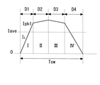
図6には、本実施例におけるマルチレベル制御で得られるリアクトル電流ILの波形の例を示す。図6は、臨界モードでの制御を前提としており、Tswはモード1~モード4からなるスイッチング周期である。また、D1~D4は各モードのデューティである。また、Ipk1はモード1における電流最大値である。
FIG. 6 shows an example of the waveform of the reactor current IL obtained by the multi-level control in this embodiment. FIG. 6 is premised on control in the critical mode, and Tsw is a switching cycle consisting of
図7には、図6に示すマルチレベル制御の電流波形を決定する際の波形決定ルーチンのフローチャートを示す。本ルーチンが実行されると、まず、ステップS101において、以下に示す式(3)によって、D1の値を決定する。
D1=Ipk1×L/(Vin×Tsw)・・・・・(3)
ここで、電流Ipk1の値は、スイッチング素子の電流容量との関係で予め決定され、ス
イッチング周期Tswは、伝送電力、効率、回路部品(定数)、制御応答のバランスから総合的に決定される。なお、周期Tswを適切に選択することで、臨界モードとすることが可能である。ステップS101の処理が終了するとステップS102に進む。
FIG. 7 shows a flowchart of the waveform determination routine for determining the current waveform of the multi-level control shown in FIG. When this routine is executed, first, in step S101, the value of D1 is determined by the following equation (3).
D1 = Ipk1 x L / (Vin x Tsw) ... (3)
Here, the value of the current Ipk1 is determined in advance in relation to the current capacity of the switching element, and the switching cycle Tsw is comprehensively determined from the balance of transmission power, efficiency, circuit components (constants), and control response. By appropriately selecting the period Tsw, it is possible to set the critical mode. When the process of step S101 is completed, the process proceeds to step S102.
ステップS102においては、D2とD3の値が、モード2とモード3の電流時間積の値が同じになるように決定される。ステップS102の処理が終了するとステップS103に進む。
In step S102, the values of D2 and D3 are determined so that the values of the current-time products of
ステップS103においては、平均電流値Iaveと、スイッチング周期Tswから伝送電
力Pを算出する。ステップS103の処理が終了するとステップS104に進む。
In step S103, the transmission power P is calculated from the average current value Iave and the switching cycle Tsw. When the process of step S103 is completed, the process proceeds to step S104.
ステップS104では、ステップS103において算出された伝送電力Pが所望の値となるように、Iave及びIpk1を調整する。 In step S104, Iave and Ipk1 are adjusted so that the transmission power P calculated in step S103 becomes a desired value.
次に、図8においては、本実施例におけるマルチレベル制御のシミュレーション結果の一例を示す。図8(a)は、図11に示した昇圧チョッパ50による臨界モードにおけるリアクトル電流ILの波形であり、スイッチング周波数fswBC=42.8kHzとしてい
る。一方、図8(b)は、図2に示したFCC10による臨界モードにおけるリアクトル電流ILの波形であり、スイッチング周波数fswFCC=30kHzとしている。また、図8(a)及び図8(b)のシミュレーション波形において、伝送電力P=1.5KW、Vdc=350V、Vfc=Vin=150v、L=100μHと共通の条件としている。
Next, FIG. 8 shows an example of the simulation result of the multi-level control in this embodiment. FIG. 8A is a waveform of the reactor current IL in the critical mode by the step-up
図8(a)に示すように、昇圧チョッパ50においては、臨界モードで、電流波形のピーク値は、20A程度と大きくなっている。一方、図8(b)に示す、FCC10のマルチレベル制御では、1スイッチング周期中のリアクトル電流ILは台形状に制御され、電流波形のピーク値を15A以下と小さくすることが可能となっている。なお、図8(b)に示す例では、モード2において、モード1におけるリアクトル電流ILの最大値が継続されている。これにより、モード1におけるリアクトル電流ILの最大値を抑えることで、より容易または確実に、1スイッチング周期中のリアクトル電流ILのピーク値を抑えられるようになっている。ここで、モード2におけるリアクトル電流ILの傾きAは、A=(Vin-Vfc)/Lと定義される(Lはリアクトル2のリアクタンス)。よって、モード2において、モード1におけるリアクトル電流ILの最大値を継続する(電流の傾きを零とする)ためには、Vin=Vfcの条件を満足させればよい。なお、Vin<Vfcの条件を満足させることで、第2モードにおけるリアクトル電流ILの傾きAをマイナスとし、モード2においてリアクトル電流ILを減少させ、モード1におけるリアクトル電流ILの最大値より小さくすることも可能である。
As shown in FIG. 8A, in the step-up
図9には、両回路方式による臨界モードにおける電流ピーク値の比較結果を示す。図9の横軸は伝送電力P、縦軸は(Ipeak×Vin)/Pで示される電流リプル比である。なお、ここでIpeakは、図8(a)においては三角波における頂点の電流値に相当する。また、図8(b)においては、モード1における電流の最大点の電流値(=Ipk1)に相当す
る。図9より、伝送電力Pが同一の場合、昇圧比αが大きくなると電流リプル比が大きくなり、平均電流値Iaveに対する電流ピークIpeakの比が大きくなることが分かる。
FIG. 9 shows a comparison result of the current peak value in the critical mode by both circuit methods. The horizontal axis of FIG. 9 is the transmission power P, and the vertical axis is the current ripple ratio represented by (Ipeak × Vin) / P. Here, Ipeak corresponds to the current value of the apex in the triangular wave in FIG. 8A. Further, in FIG. 8B, it corresponds to the current value (= Ipk1) at the maximum point of the current in
これは、昇圧比αが大きくなると、リアクトルへの充電モードであるモード1の期間D1が長くなり、電流ピーク値が大きくことに起因する。また、図9中、両回路方式における昇圧比α=2.33の場合の曲線を比較して分かるように、昇圧比αが同一の場合は、伝送電力Pが小さくなると、昇圧チョッパ50と、FCC10との電流ピーク値の差が大きくなる傾向が見られた。図9より、今回の昇圧比α及び伝送電力Pの範囲においては、両回路構成における伝送電力P及びリアクトルが同じ条件となる場合、昇圧チョッパ50に比較してFCC10では、電流リプル比を最大38.3%低減できることが分かった。これにより、リアクトル2及び、スイッチング回路3の各スイッチング素子3a~3dの電流容量を可及的に低減することができ、装置の大きさや装置コストを大幅に低減することが可能となる。
This is because when the step-up ratio α becomes large, the period D1 of the
なお、上記のシミュレーションは臨界モードで行ったが、本発明は臨界モードでない重負荷時や軽負荷時にも適用可能である。図10には、本実施例における制御を、重負荷時
、臨界モード、軽負荷時にそれぞれ適用した場合の波形のイメージを示す。図10(a)は重負荷時、図10(b)は臨界モード、図10(c)は軽負荷時に適用した場合の電流波形である。
Although the above simulation was performed in the critical mode, the present invention can be applied to a heavy load or a light load which is not the critical mode. FIG. 10 shows an image of a waveform when the control in this embodiment is applied under heavy load, critical mode, and light load, respectively. 10 (a) is a current waveform when applied under heavy load, FIG. 10 (b) is a critical mode, and FIG. 10 (c) is a light load.
重負荷時または軽負荷時に本発明を適用する場合にも、入力電圧Vinと出力電圧Vdcが変化しなければ、スイッチング周波数を変化させて臨界モードとした上で、マルチレベル制御を行っても構わない。リアクトル電流ILの波形を臨界モードとすることで、単純な電流制御方法によって、リアクトル電流ILのピーク値を可及的に低く抑えることが可能となる。 Even when the present invention is applied under heavy load or light load, if the input voltage Vin and the output voltage Vdc do not change, multi-level control may be performed after changing the switching frequency to the critical mode. do not have. By setting the waveform of the reactor current IL to the critical mode, it is possible to suppress the peak value of the reactor current IL as low as possible by a simple current control method.
上記の実施例で説明した内容は本発明の例示に過ぎない。上記の実施例で例示した内容の他、本発明の趣旨を逸脱しない範囲で、実施例の内容を適宜変更が可能なことは当然である。例えば、図8(b)で示したマルチレベル制御では、モード2においては、モード1におけるリアクトル電流ILのピーク値を維持し、電流波形が台形となるようにしたが、マルチレベル制御における電流波形の形状は必ずしも台形でなくてもよい。図6または図10に示したように、モード2においてリアクトル電流ILの値が変化するようにしても構わない。
The contents described in the above examples are merely examples of the present invention. In addition to the contents illustrated in the above examples, it is natural that the contents of the examples can be appropriately changed without departing from the spirit of the present invention. For example, in the multi-level control shown in FIG. 8 (b), in
また、例えば、上記の実施例では、実際のリアクトル電流ILを電流センサ6で検出し、検出値が例えば図7の波形決定ルーチンで決められた値となるように、制御回路7によってフィードバック制御することを前提としたが、電流センサ6で実際のリアクトル電流ILを検出せず、設計値に基づいて制御回路7がスイッチング回路3における各スイッチング素子3a~3dのオンオフをオープン制御しても構わない。さらに、入力電流の平均値Iave(=P/Vin)を用いてフィードバック制御することで、リアクトル電流ILを
制御しても構わない。
Further, for example, in the above embodiment, the actual reactor current IL is detected by the
また、上記の適用例及び実施例においては、制御回路7は、DC-DCコンバータ10が備える構成としたが、インバータ回路103におけるスイッチング素子の制御回路も含めてパワーコンディショナ101が備える構成としてもよい。
Further, in the above application examples and embodiments, the control circuit 7 has a configuration provided in the DC-
なお、以下には本発明の構成要件と実施例の構成とを対比可能とするために、本発明の構成要件を図面の符号付きで記載しておく。
<発明1>
直流入力電圧を昇圧して直流出力電圧とするDC-DCコンバータ(10)であって、
前記直流出力電圧を出力する出力部(5)に両端が接続され、4つのスイッチング素子が、第1スイッチング素子(3a)、第2スイッチング素子(3b)、第3スイッチング素子(3c)及び第4スイッチング素子(3d)の順番で直列に接続されたスイッチング回路(3)と、
前記第1スイッチング素子(3a)と前記第2スイッチング素子(3b)との接続部と、前記第3スイッチング素子(3c)と前記第4スイッチング素子(3d)との接続部との間に接続されたフライングキャパシタ(4)と、
前記第2スイッチング素子(3b)と前記第3スイッチング素子(3c)との接続部と、前記直流入力電圧が入力される入力部(1)の正極との間に接続されたリアクトル(2)と、
所定のタイミングで前記スイッチング回路における前記各スイッチング素子をオンオフさせる制御回路(7)と、
を備え、
前記制御回路(7)は、前記リアクトルに流れるリアクトル電流における最大値が所定値以下となるように、前記各スイッチング素子(3a~3d)をオンオフさせることを特徴とするDC-DCコンバータ。
<発明2>
前記スイッチング回路(3)における前記第1スイッチング素子(3a)と前記第2スイッチング素子(3b)がオフし前記第3スイッチング素子(3c)と前記第4スイッチング素子(3d)がオンする第1モードと、前記第1スイッチング素子(3a)と前記第3スイッチング素子(3c)がオフし前記第2スイッチング素子(3b)と前記第4スイッチング素子(3d)がオンする第2モードと、前記第2スイッチング素子(3b)と前記第4スイッチング素子(3d)がオフし前記第1スイッチング素子(3a)と前記第3スイッチング素子(3c)がオンする第3モードと、前記第3スイッチング素子(3c)と前記第4スイッチング素子(3d)がオフし前記第1スイッチング素子(3a)と前記第2スイッチング素子(3b)がオンする第4モードと、を有し、
前記制御回路(7)は、前記第1モードにおける前記リアクトル電流の最大値が、前記スイッチング回路(3)における各スイッチング素子(3a~3d)の電流容量に係る電流未満となるように、前記第1モードの期間を決定することを特徴とする、発明1に係るDC-DCコンバータ。
<発明3>
前記第2モードと前記第3モードにおける前記リアクトル電流の電流時間積が同等となるように、前記第2モード及び前記第3モードの期間が決定されることを特徴とする発明2に係るDC-DCコンバータ。
<発明4>
前記第2モードにおける、前記リアクトル電流の値として、前記第1モードにおける前記リアクトル電流の最大値が継続されることを特徴とする発明2または3に係るDC-DCコンバータ。
<発明5>
前記リアクトル電流が前記スイッチング回路側から前記入力部側に流れる場合には、前記リアクトル電流を零とする、電流不連続モードが適用されることを特徴とする、発明1から4のいずれかに係るDC-DCコンバータ。
<発明6>
発明1から5のいずれかに係るDC-DCコンバータと、
前記DC-DCコンバータの出力を交流に変換するインバータ回路と、
を備えるパワーコンディショナ。
In addition, in order to make it possible to compare the constituent elements of the present invention with the configurations of the examples, the constituent elements of the present invention are described below with reference numerals in the drawings.
<
A DC-DC converter (10) that boosts a DC input voltage to a DC output voltage.
Both ends are connected to the output unit (5) that outputs the DC output voltage, and the four switching elements are the first switching element (3a), the second switching element (3b), the third switching element (3c), and the fourth. A switching circuit (3) connected in series in the order of the switching elements (3d), and
It is connected between the connection portion between the first switching element (3a) and the second switching element (3b) and the connection portion between the third switching element (3c) and the fourth switching element (3d). Flying capacitor (4) and
A reactor (2) connected between the connection portion between the second switching element (3b) and the third switching element (3c) and the positive electrode of the input portion (1) to which the DC input voltage is input. ,
A control circuit (7) that turns each switching element in the switching circuit on and off at a predetermined timing, and
Equipped with
The control circuit (7) is a DC-DC converter characterized in that each of the switching elements (3a to 3d) is turned on and off so that the maximum value of the reactor current flowing through the reactor is equal to or less than a predetermined value.
<
A first mode in which the first switching element (3a) and the second switching element (3b) in the switching circuit (3) are turned off and the third switching element (3c) and the fourth switching element (3d) are turned on. A second mode in which the first switching element (3a) and the third switching element (3c) are turned off and the second switching element (3b) and the fourth switching element (3d) are turned on, and the second mode. A third mode in which the switching element (3b) and the fourth switching element (3d) are turned off and the first switching element (3a) and the third switching element (3c) are turned on, and the third switching element (3c). And a fourth mode in which the fourth switching element (3d) is turned off and the first switching element (3a) and the second switching element (3b) are turned on.
The control circuit (7) has the first mode so that the maximum value of the reactor current in the first mode is less than the current related to the current capacity of each switching element (3a to 3d) in the switching circuit (3). The DC-DC converter according to the
<
The DC-DC according to the
<
The DC-DC converter according to the
<
2. DC-DC converter.
<
The DC-DC converter according to any one of the
An inverter circuit that converts the output of the DC-DC converter into alternating current,
Power conditioner with.
1・・・入力部
2・・・リアクトル
3・・・スイッチング回路
3a~3d・・・スイッチング素子
4・・・フライングキャパシタ
5・・・出力部
6・・・電流センサ
7・・・制御回路
10・・・DC-DCコンバータ
50・・・昇圧チョッパ
100・・・発電システム
101・・・パワーコンディショナ
102・・・発電装置
103・・・インバータ回路
104・・・制御回路
105・・・系統
1 ...
Claims (4)
前記直流出力電圧を出力する出力部に両端が接続され、4つのスイッチング素子が、第1スイッチング素子、第2スイッチング素子、第3スイッチング素子及び第4スイッチング素子の順番で直列に接続されたスイッチング回路と、
前記第1スイッチング素子と前記第2スイッチング素子との接続部と、前記第3スイッチング素子と前記第4スイッチング素子との接続部との間に接続されたフライングキャパシタと、
前記第2スイッチング素子と前記第3スイッチング素子との接続部と、前記直流入力電圧が入力される入力部の正極との間に接続されたリアクトルと、
所定のタイミングで前記スイッチング回路における前記各スイッチング素子をオンオフさせる制御回路と、
を備え、
前記制御回路は、前記リアクトルに流れるリアクトル電流における最大値が所定値以下となるように、前記各スイッチング素子をオンオフさせ、
前記スイッチング回路における前記第1スイッチング素子と前記第2スイッチング素子がオフし前記第3スイッチング素子と前記第4スイッチング素子がオンする第1モードと、前記第1スイッチング素子と前記第3スイッチング素子がオフし前記第2スイッチング素子と前記第4スイッチング素子がオンする第2モードと、前記第2スイッチング素子と前記第4スイッチング素子がオフし前記第1スイッチング素子と前記第3スイッチング素子がオンする第3モードと、前記第3スイッチング素子と前記第4スイッチング素子がオフし前記第1スイッチング素子と前記第2スイッチング素子がオンする第4モードと、を有し、
前記制御回路は、前記第1モードにおける前記リアクトル電流の最大値が、前記スイッチング回路における各スイッチング素子の電流容量に係る電流未満となるように、前記第1モードの期間を決定し、前記第2モードと前記第3モードにおける前記リアクトル電流の電流時間積が同等となるように、前記第2モード及び前記第3モードの期間が決定されることを特徴とするDC-DCコンバータ。 A DC-DC converter that boosts the DC input voltage to the DC output voltage.
A switching circuit in which both ends are connected to an output unit that outputs a DC output voltage, and four switching elements are connected in series in the order of a first switching element, a second switching element, a third switching element, and a fourth switching element. When,
A flying capacitor connected between the connection portion between the first switching element and the second switching element and the connection portion between the third switching element and the fourth switching element.
A reactor connected between the connection portion between the second switching element and the third switching element and the positive electrode of the input portion to which the DC input voltage is input.
A control circuit that turns each switching element in the switching circuit on and off at a predetermined timing,
Equipped with
The control circuit turns each switching element on and off so that the maximum value of the reactor current flowing through the reactor is equal to or less than a predetermined value.
In the switching circuit, the first mode in which the first switching element and the second switching element are turned off and the third switching element and the fourth switching element are turned on, and the first switching element and the third switching element are turned off. A second mode in which the second switching element and the fourth switching element are turned on, and a third mode in which the second switching element and the fourth switching element are turned off and the first switching element and the third switching element are turned on. It has a mode and a fourth mode in which the third switching element and the fourth switching element are turned off and the first switching element and the second switching element are turned on.
The control circuit determines the period of the first mode so that the maximum value of the reactor current in the first mode is less than the current related to the current capacity of each switching element in the switching circuit, and the second mode. A DC-DC converter characterized in that the periods of the second mode and the third mode are determined so that the current-time product of the reactor currents in the mode and the third mode are equivalent .
前記DC-DCコンバータの出力を交流に変換するインバータ回路と、
を備えるパワーコンディショナ。 The DC-DC converter according to any one of claims 1 to 3 .
An inverter circuit that converts the output of the DC-DC converter into alternating current,
Power conditioner with.
Priority Applications (3)
| Application Number | Priority Date | Filing Date | Title |
|---|---|---|---|
| JP2017217769A JP7001896B2 (en) | 2017-11-10 | 2017-11-10 | DC-DC converter |
| TW107132705A TWI694668B (en) | 2017-11-10 | 2018-09-17 | DC-DC converter and power conditioner |
| US16/133,650 US10461637B2 (en) | 2017-11-10 | 2018-09-17 | DC-DC converter |
Applications Claiming Priority (1)
| Application Number | Priority Date | Filing Date | Title |
|---|---|---|---|
| JP2017217769A JP7001896B2 (en) | 2017-11-10 | 2017-11-10 | DC-DC converter |
Publications (2)
| Publication Number | Publication Date |
|---|---|
| JP2019092242A JP2019092242A (en) | 2019-06-13 |
| JP7001896B2 true JP7001896B2 (en) | 2022-01-20 |
Family
ID=66433596
Family Applications (1)
| Application Number | Title | Priority Date | Filing Date |
|---|---|---|---|
| JP2017217769A Active JP7001896B2 (en) | 2017-11-10 | 2017-11-10 | DC-DC converter |
Country Status (3)
| Country | Link |
|---|---|
| US (1) | US10461637B2 (en) |
| JP (1) | JP7001896B2 (en) |
| TW (1) | TWI694668B (en) |
Families Citing this family (4)
| Publication number | Priority date | Publication date | Assignee | Title |
|---|---|---|---|---|
| JP6789654B2 (en) * | 2016-04-04 | 2020-11-25 | 東芝キヤリア株式会社 | Power supply |
| KR20210151523A (en) * | 2020-06-05 | 2021-12-14 | 엘지이노텍 주식회사 | Converter |
| TWI766314B (en) * | 2020-07-21 | 2022-06-01 | 茂達電子股份有限公司 | Power converter with automatic balance mechanism of flying capacitor |
| KR102633213B1 (en) * | 2021-04-22 | 2024-02-05 | 엘에스일렉트릭(주) | Dc-dc converter |
Citations (4)
| Publication number | Priority date | Publication date | Assignee | Title |
|---|---|---|---|---|
| JP2013192383A (en) | 2012-03-14 | 2013-09-26 | Sanken Electric Co Ltd | Dc-dc converter |
| JP2015019480A (en) | 2013-07-10 | 2015-01-29 | 三菱電機株式会社 | Power conversion apparatus and control method for the same |
| JP2017169393A (en) | 2016-03-17 | 2017-09-21 | 三菱電機株式会社 | Controller of dc/dc converter and control method |
| US20170324321A1 (en) | 2016-05-06 | 2017-11-09 | Merus Audio Aps | Load adaptable boost dc-dc power converter |
Family Cites Families (9)
| Publication number | Priority date | Publication date | Assignee | Title |
|---|---|---|---|---|
| SE525546C2 (en) * | 2002-08-16 | 2005-03-08 | Abb Ab | A plant for transmitting electrical power and a method for operating such a plant |
| JP5457559B2 (en) * | 2010-07-30 | 2014-04-02 | 三菱電機株式会社 | DC / DC converter |
| JP5492040B2 (en) * | 2010-09-22 | 2014-05-14 | 株式会社豊田中央研究所 | Power system |
| KR101651161B1 (en) * | 2011-03-29 | 2016-08-25 | 후지필름 가부시키가이샤 | Optical film for 3d image display, 3d image display device, and 3d image display system |
| JP5859758B2 (en) * | 2011-07-05 | 2016-02-16 | ルネサスエレクトロニクス株式会社 | Manufacturing method of semiconductor device |
| US20130013478A1 (en) * | 2011-07-08 | 2013-01-10 | Jonathan Broadbent | System and method for incentivizing retirement savings |
| JP5644786B2 (en) * | 2012-01-25 | 2014-12-24 | トヨタ自動車株式会社 | Control device for voltage converter |
| DE102014104730A1 (en) * | 2014-04-03 | 2015-10-08 | Sma Solar Technology Ag | Method for reducing interference emissions of a current or voltage converter with clocked circuit breakers |
| CN106787877B (en) * | 2016-12-13 | 2019-03-05 | 清华大学 | Antithesis unipolar voltage module chain and its mixed multi-level current transformer |
-
2017
- 2017-11-10 JP JP2017217769A patent/JP7001896B2/en active Active
-
2018
- 2018-09-17 US US16/133,650 patent/US10461637B2/en active Active
- 2018-09-17 TW TW107132705A patent/TWI694668B/en active
Patent Citations (4)
| Publication number | Priority date | Publication date | Assignee | Title |
|---|---|---|---|---|
| JP2013192383A (en) | 2012-03-14 | 2013-09-26 | Sanken Electric Co Ltd | Dc-dc converter |
| JP2015019480A (en) | 2013-07-10 | 2015-01-29 | 三菱電機株式会社 | Power conversion apparatus and control method for the same |
| JP2017169393A (en) | 2016-03-17 | 2017-09-21 | 三菱電機株式会社 | Controller of dc/dc converter and control method |
| US20170324321A1 (en) | 2016-05-06 | 2017-11-09 | Merus Audio Aps | Load adaptable boost dc-dc power converter |
Also Published As
| Publication number | Publication date |
|---|---|
| US10461637B2 (en) | 2019-10-29 |
| TWI694668B (en) | 2020-05-21 |
| JP2019092242A (en) | 2019-06-13 |
| US20190149044A1 (en) | 2019-05-16 |
| TW201919319A (en) | 2019-05-16 |
Similar Documents
| Publication | Publication Date | Title |
|---|---|---|
| US9294001B2 (en) | Power converter with dead-time control function | |
| US9667153B2 (en) | Switching power supply apparatus for generating control signal for lowering switching frequency of switching devices | |
| JP7001896B2 (en) | DC-DC converter | |
| EP2963798B1 (en) | Dc-ac conversion device and control circuit | |
| CN102362419B (en) | Control device for transformer coupling type booster | |
| WO2011016199A1 (en) | Dc/dc power converter | |
| US8488346B2 (en) | Power conversion apparatus and method | |
| JP5491809B2 (en) | Grid-connected inverter device | |
| US20190260306A1 (en) | Power converter | |
| US20140211515A1 (en) | Dc-dc converter and power supply device having dc-dc converter | |
| JP2016163386A (en) | Power conversion device | |
| JP2008199808A (en) | System-interconnected inverter arrangement | |
| JP7090745B2 (en) | Power converter and DC distribution system | |
| WO2018110440A1 (en) | Snubber circuit and power conversion system using same | |
| US8824180B2 (en) | Power conversion apparatus | |
| JP6012822B1 (en) | Power converter | |
| JP2010088150A (en) | Charger | |
| JP7124297B2 (en) | power converter | |
| KR20140143908A (en) | Mehtod for controlling duty of Low Voltage DC/DC Converter | |
| US20160118904A1 (en) | Power conversion apparatus | |
| JP2005287249A (en) | Switching power supply | |
| JP2012029362A (en) | Power supply circuit | |
| JP2012222951A (en) | Charging device | |
| KR20190115364A (en) | Single and three phase combined charger | |
| CN106817019A (en) | Apparatus and method for controlling the low-voltage direct converter of environment-friendly type vehicle |
Legal Events
| Date | Code | Title | Description |
|---|---|---|---|
| A621 | Written request for application examination |
Free format text: JAPANESE INTERMEDIATE CODE: A621 Effective date: 20201014 |
|
| A977 | Report on retrieval |
Free format text: JAPANESE INTERMEDIATE CODE: A971007 Effective date: 20210820 |
|
| A131 | Notification of reasons for refusal |
Free format text: JAPANESE INTERMEDIATE CODE: A131 Effective date: 20210831 |
|
| A521 | Written amendment |
Free format text: JAPANESE INTERMEDIATE CODE: A523 Effective date: 20211101 |
|
| TRDD | Decision of grant or rejection written | ||
| A01 | Written decision to grant a patent or to grant a registration (utility model) |
Free format text: JAPANESE INTERMEDIATE CODE: A01 Effective date: 20211116 |
|
| A61 | First payment of annual fees (during grant procedure) |
Free format text: JAPANESE INTERMEDIATE CODE: A61 Effective date: 20211130 |
|
| R150 | Certificate of patent or registration of utility model |
Ref document number: 7001896 Country of ref document: JP Free format text: JAPANESE INTERMEDIATE CODE: R150 |