WO2018110440A1 - Snubber circuit and power conversion system using same - Google Patents
Snubber circuit and power conversion system using same Download PDFInfo
- Publication number
- WO2018110440A1 WO2018110440A1 PCT/JP2017/044107 JP2017044107W WO2018110440A1 WO 2018110440 A1 WO2018110440 A1 WO 2018110440A1 JP 2017044107 W JP2017044107 W JP 2017044107W WO 2018110440 A1 WO2018110440 A1 WO 2018110440A1
- Authority
- WO
- WIPO (PCT)
- Prior art keywords
- voltage
- circuit
- clamp
- pair
- points
- Prior art date
Links
Images


Classifications
-
- H—ELECTRICITY
- H02—GENERATION; CONVERSION OR DISTRIBUTION OF ELECTRIC POWER
- H02M—APPARATUS FOR CONVERSION BETWEEN AC AND AC, BETWEEN AC AND DC, OR BETWEEN DC AND DC, AND FOR USE WITH MAINS OR SIMILAR POWER SUPPLY SYSTEMS; CONVERSION OF DC OR AC INPUT POWER INTO SURGE OUTPUT POWER; CONTROL OR REGULATION THEREOF
- H02M1/00—Details of apparatus for conversion
- H02M1/32—Means for protecting converters other than automatic disconnection
- H02M1/34—Snubber circuits
- H02M1/342—Active non-dissipative snubbers
-
- H—ELECTRICITY
- H02—GENERATION; CONVERSION OR DISTRIBUTION OF ELECTRIC POWER
- H02M—APPARATUS FOR CONVERSION BETWEEN AC AND AC, BETWEEN AC AND DC, OR BETWEEN DC AND DC, AND FOR USE WITH MAINS OR SIMILAR POWER SUPPLY SYSTEMS; CONVERSION OF DC OR AC INPUT POWER INTO SURGE OUTPUT POWER; CONTROL OR REGULATION THEREOF
- H02M1/00—Details of apparatus for conversion
- H02M1/32—Means for protecting converters other than automatic disconnection
- H02M1/34—Snubber circuits
-
- H—ELECTRICITY
- H02—GENERATION; CONVERSION OR DISTRIBUTION OF ELECTRIC POWER
- H02M—APPARATUS FOR CONVERSION BETWEEN AC AND AC, BETWEEN AC AND DC, OR BETWEEN DC AND DC, AND FOR USE WITH MAINS OR SIMILAR POWER SUPPLY SYSTEMS; CONVERSION OF DC OR AC INPUT POWER INTO SURGE OUTPUT POWER; CONTROL OR REGULATION THEREOF
- H02M3/00—Conversion of dc power input into dc power output
- H02M3/22—Conversion of dc power input into dc power output with intermediate conversion into ac
- H02M3/24—Conversion of dc power input into dc power output with intermediate conversion into ac by static converters
- H02M3/28—Conversion of dc power input into dc power output with intermediate conversion into ac by static converters using discharge tubes with control electrode or semiconductor devices with control electrode to produce the intermediate ac
- H02M3/325—Conversion of dc power input into dc power output with intermediate conversion into ac by static converters using discharge tubes with control electrode or semiconductor devices with control electrode to produce the intermediate ac using devices of a triode or a transistor type requiring continuous application of a control signal
- H02M3/335—Conversion of dc power input into dc power output with intermediate conversion into ac by static converters using discharge tubes with control electrode or semiconductor devices with control electrode to produce the intermediate ac using devices of a triode or a transistor type requiring continuous application of a control signal using semiconductor devices only
- H02M3/33569—Conversion of dc power input into dc power output with intermediate conversion into ac by static converters using discharge tubes with control electrode or semiconductor devices with control electrode to produce the intermediate ac using devices of a triode or a transistor type requiring continuous application of a control signal using semiconductor devices only having several active switching elements
- H02M3/33576—Conversion of dc power input into dc power output with intermediate conversion into ac by static converters using discharge tubes with control electrode or semiconductor devices with control electrode to produce the intermediate ac using devices of a triode or a transistor type requiring continuous application of a control signal using semiconductor devices only having several active switching elements having at least one active switching element at the secondary side of an isolation transformer
- H02M3/33584—Bidirectional converters
-
- H—ELECTRICITY
- H02—GENERATION; CONVERSION OR DISTRIBUTION OF ELECTRIC POWER
- H02M—APPARATUS FOR CONVERSION BETWEEN AC AND AC, BETWEEN AC AND DC, OR BETWEEN DC AND DC, AND FOR USE WITH MAINS OR SIMILAR POWER SUPPLY SYSTEMS; CONVERSION OF DC OR AC INPUT POWER INTO SURGE OUTPUT POWER; CONTROL OR REGULATION THEREOF
- H02M3/00—Conversion of dc power input into dc power output
- H02M3/22—Conversion of dc power input into dc power output with intermediate conversion into ac
- H02M3/24—Conversion of dc power input into dc power output with intermediate conversion into ac by static converters
- H02M3/28—Conversion of dc power input into dc power output with intermediate conversion into ac by static converters using discharge tubes with control electrode or semiconductor devices with control electrode to produce the intermediate ac
- H02M3/325—Conversion of dc power input into dc power output with intermediate conversion into ac by static converters using discharge tubes with control electrode or semiconductor devices with control electrode to produce the intermediate ac using devices of a triode or a transistor type requiring continuous application of a control signal
- H02M3/335—Conversion of dc power input into dc power output with intermediate conversion into ac by static converters using discharge tubes with control electrode or semiconductor devices with control electrode to produce the intermediate ac using devices of a triode or a transistor type requiring continuous application of a control signal using semiconductor devices only
- H02M3/337—Conversion of dc power input into dc power output with intermediate conversion into ac by static converters using discharge tubes with control electrode or semiconductor devices with control electrode to produce the intermediate ac using devices of a triode or a transistor type requiring continuous application of a control signal using semiconductor devices only in push-pull configuration
- H02M3/3376—Conversion of dc power input into dc power output with intermediate conversion into ac by static converters using discharge tubes with control electrode or semiconductor devices with control electrode to produce the intermediate ac using devices of a triode or a transistor type requiring continuous application of a control signal using semiconductor devices only in push-pull configuration with automatic control of output voltage or current
-
- H—ELECTRICITY
- H02—GENERATION; CONVERSION OR DISTRIBUTION OF ELECTRIC POWER
- H02M—APPARATUS FOR CONVERSION BETWEEN AC AND AC, BETWEEN AC AND DC, OR BETWEEN DC AND DC, AND FOR USE WITH MAINS OR SIMILAR POWER SUPPLY SYSTEMS; CONVERSION OF DC OR AC INPUT POWER INTO SURGE OUTPUT POWER; CONTROL OR REGULATION THEREOF
- H02M7/00—Conversion of ac power input into dc power output; Conversion of dc power input into ac power output
- H02M7/42—Conversion of dc power input into ac power output without possibility of reversal
- H02M7/44—Conversion of dc power input into ac power output without possibility of reversal by static converters
- H02M7/48—Conversion of dc power input into ac power output without possibility of reversal by static converters using discharge tubes with control electrode or semiconductor devices with control electrode
- H02M7/53—Conversion of dc power input into ac power output without possibility of reversal by static converters using discharge tubes with control electrode or semiconductor devices with control electrode using devices of a triode or transistor type requiring continuous application of a control signal
- H02M7/537—Conversion of dc power input into ac power output without possibility of reversal by static converters using discharge tubes with control electrode or semiconductor devices with control electrode using devices of a triode or transistor type requiring continuous application of a control signal using semiconductor devices only, e.g. single switched pulse inverters
- H02M7/5387—Conversion of dc power input into ac power output without possibility of reversal by static converters using discharge tubes with control electrode or semiconductor devices with control electrode using devices of a triode or transistor type requiring continuous application of a control signal using semiconductor devices only, e.g. single switched pulse inverters in a bridge configuration
-
- H—ELECTRICITY
- H02—GENERATION; CONVERSION OR DISTRIBUTION OF ELECTRIC POWER
- H02M—APPARATUS FOR CONVERSION BETWEEN AC AND AC, BETWEEN AC AND DC, OR BETWEEN DC AND DC, AND FOR USE WITH MAINS OR SIMILAR POWER SUPPLY SYSTEMS; CONVERSION OF DC OR AC INPUT POWER INTO SURGE OUTPUT POWER; CONTROL OR REGULATION THEREOF
- H02M1/00—Details of apparatus for conversion
- H02M1/0067—Converter structures employing plural converter units, other than for parallel operation of the units on a single load
- H02M1/007—Plural converter units in cascade
-
- H—ELECTRICITY
- H02—GENERATION; CONVERSION OR DISTRIBUTION OF ELECTRIC POWER
- H02M—APPARATUS FOR CONVERSION BETWEEN AC AND AC, BETWEEN AC AND DC, OR BETWEEN DC AND DC, AND FOR USE WITH MAINS OR SIMILAR POWER SUPPLY SYSTEMS; CONVERSION OF DC OR AC INPUT POWER INTO SURGE OUTPUT POWER; CONTROL OR REGULATION THEREOF
- H02M3/00—Conversion of dc power input into dc power output
- H02M3/02—Conversion of dc power input into dc power output without intermediate conversion into ac
- H02M3/04—Conversion of dc power input into dc power output without intermediate conversion into ac by static converters
- H02M3/10—Conversion of dc power input into dc power output without intermediate conversion into ac by static converters using discharge tubes with control electrode or semiconductor devices with control electrode
- H02M3/145—Conversion of dc power input into dc power output without intermediate conversion into ac by static converters using discharge tubes with control electrode or semiconductor devices with control electrode using devices of a triode or transistor type requiring continuous application of a control signal
- H02M3/155—Conversion of dc power input into dc power output without intermediate conversion into ac by static converters using discharge tubes with control electrode or semiconductor devices with control electrode using devices of a triode or transistor type requiring continuous application of a control signal using semiconductor devices only
- H02M3/156—Conversion of dc power input into dc power output without intermediate conversion into ac by static converters using discharge tubes with control electrode or semiconductor devices with control electrode using devices of a triode or transistor type requiring continuous application of a control signal using semiconductor devices only with automatic control of output voltage or current, e.g. switching regulators
- H02M3/158—Conversion of dc power input into dc power output without intermediate conversion into ac by static converters using discharge tubes with control electrode or semiconductor devices with control electrode using devices of a triode or transistor type requiring continuous application of a control signal using semiconductor devices only with automatic control of output voltage or current, e.g. switching regulators including plural semiconductor devices as final control devices for a single load
-
- H—ELECTRICITY
- H02—GENERATION; CONVERSION OR DISTRIBUTION OF ELECTRIC POWER
- H02M—APPARATUS FOR CONVERSION BETWEEN AC AND AC, BETWEEN AC AND DC, OR BETWEEN DC AND DC, AND FOR USE WITH MAINS OR SIMILAR POWER SUPPLY SYSTEMS; CONVERSION OF DC OR AC INPUT POWER INTO SURGE OUTPUT POWER; CONTROL OR REGULATION THEREOF
- H02M7/00—Conversion of ac power input into dc power output; Conversion of dc power input into ac power output
- H02M7/66—Conversion of ac power input into dc power output; Conversion of dc power input into ac power output with possibility of reversal
- H02M7/68—Conversion of ac power input into dc power output; Conversion of dc power input into ac power output with possibility of reversal by static converters
- H02M7/72—Conversion of ac power input into dc power output; Conversion of dc power input into ac power output with possibility of reversal by static converters using discharge tubes with control electrode or semiconductor devices with control electrode
- H02M7/79—Conversion of ac power input into dc power output; Conversion of dc power input into ac power output with possibility of reversal by static converters using discharge tubes with control electrode or semiconductor devices with control electrode using devices of a triode or transistor type requiring continuous application of a control signal
- H02M7/797—Conversion of ac power input into dc power output; Conversion of dc power input into ac power output with possibility of reversal by static converters using discharge tubes with control electrode or semiconductor devices with control electrode using devices of a triode or transistor type requiring continuous application of a control signal using semiconductor devices only
-
- Y—GENERAL TAGGING OF NEW TECHNOLOGICAL DEVELOPMENTS; GENERAL TAGGING OF CROSS-SECTIONAL TECHNOLOGIES SPANNING OVER SEVERAL SECTIONS OF THE IPC; TECHNICAL SUBJECTS COVERED BY FORMER USPC CROSS-REFERENCE ART COLLECTIONS [XRACs] AND DIGESTS
- Y02—TECHNOLOGIES OR APPLICATIONS FOR MITIGATION OR ADAPTATION AGAINST CLIMATE CHANGE
- Y02B—CLIMATE CHANGE MITIGATION TECHNOLOGIES RELATED TO BUILDINGS, e.g. HOUSING, HOUSE APPLIANCES OR RELATED END-USER APPLICATIONS
- Y02B70/00—Technologies for an efficient end-user side electric power management and consumption
- Y02B70/10—Technologies improving the efficiency by using switched-mode power supplies [SMPS], i.e. efficient power electronics conversion e.g. power factor correction or reduction of losses in power supplies or efficient standby modes
Definitions
- the present disclosure relates generally to a snubber circuit and a power conversion system using the snubber circuit, and more particularly to a snubber circuit for suppressing ringing or surge voltage and power conversion using the snubber circuit About the system.
- Patent Document 1 describes that a snubber circuit is used in a power conversion system such as an AC / DC power converter.
- an AC / AC frequency converter connected to the primary side of a high-frequency transformer has a three-phase rectifier, an inverter, and a snubber circuit.
- the input side of the three-phase rectifier is connected to a three-phase commercial AC power source, and the output side is connected to the input side of the inverter.
- the input side of the inverter is connected to the output side of the three-phase rectifier, and the output side is connected to the primary side of the high-frequency transformer.
- the snubber circuit is connected between the three-phase rectifier and the inverter.
- the snubber circuit described in Patent Document 1 absorbs spike-like overvoltage generated by leakage inductance of a high-frequency transformer as energy, and regenerates the absorbed energy.
- This snubber circuit is a regenerative RCD unidirectional snubber circuit composed of a resistor, a capacitor, a diode, and a semiconductor switch.
- This disclosure has been made in view of the above reasons, and an object thereof is to provide a snubber circuit capable of suppressing loss and a power conversion system using the snubber circuit.
- the snubber circuit includes a first clamp circuit, a second clamp circuit, and a voltage conversion circuit.
- the first clamp circuit absorbs electric energy of the main circuit from the pair of first voltage points when the magnitude of the voltage between the pair of first voltage points in the main circuit exceeds a first clamp value. Accordingly, the first clamp circuit clamps the voltage between the pair of first voltage points to the first clamp value.
- the second clamp circuit injects electric energy from the pair of second voltage points to the main circuit when the magnitude of the voltage between the pair of second voltage points in the main circuit is lower than a second clamp value. . Thereby, the second clamp circuit clamps the voltage between the pair of second voltage points to the second clamp value.
- the voltage conversion circuit is electrically connected to the first clamp circuit and the second clamp circuit, and includes a first clamp voltage defining the first clamp value and a second clamp voltage defining the second clamp value. Voltage conversion between the two.
- the snubber circuit according to a second aspect is the first aspect, wherein the first voltage point on the high potential side of the pair of first voltage points and the second voltage point on the high potential side of the pair of second voltage points are Are at the same potential. In this case, the first voltage point on the low potential side of the pair of first voltage points and the second voltage point on the low potential side of the pair of second voltage points have the same potential.
- the voltage conversion circuit is configured to step down the first clamp voltage and generate the second clamp voltage.
- a snubber circuit is the DC / DC converter according to the first or second aspect, wherein the voltage conversion circuit includes a semiconductor switch, an inductor, and a capacitive element.
- the capacitive element is electrically connected in parallel with at least one of the semiconductor switch and the inductor.
- a snubber circuit is the snubber circuit according to any one of the first to third aspects, wherein the first clamp circuit includes a first diode electrically connected in series between the pair of first voltage points, and a first diode. One capacitor is included. In this case, the first clamp circuit causes a current to flow from the main circuit to the first capacitive element through the first diode when the voltage between the pair of first voltage points exceeds the first clamp value. It is configured.
- the second clamp circuit includes a second diode and a second capacitive element that are electrically connected in series between the pair of second voltage points. In this case, the second clamp circuit causes a current to flow from the second capacitive element to the main circuit through the second diode when a voltage between the pair of second voltage points is lower than the second clamp value. It is configured.
- a snubber circuit is the DC / DC converter according to any one of the first to fourth aspects, wherein the voltage conversion circuit includes a semiconductor switch and an inductor.
- the voltage conversion circuit is configured to switch the semiconductor switch so that an inductor current flowing through the inductor is in a discontinuous mode.
- the snubber circuit according to a sixth aspect is the DC / DC converter according to any one of the first to fifth aspects, wherein the voltage conversion circuit includes a semiconductor switch, an inductor, and a control circuit that controls the semiconductor switch. It is.
- the control circuit is configured to adjust the first clamp value and the second clamp value by adjusting a duty ratio of the semiconductor switch.
- a power conversion system includes a snubber circuit according to any one of the first to sixth aspects and the main circuit, and the main circuit is a power conversion circuit that performs power conversion.
- the main circuit includes two or more primary terminals, two or more secondary terminals, and a high-frequency insulating transformer.
- the main circuit is configured to perform power conversion between the two or more primary terminals and the two or more secondary terminals via the high-frequency insulating transformer.
- the snubber circuit is electrically connected to the high-frequency insulating transformer.
- FIG. 1 is a circuit diagram of a power conversion system according to an embodiment of the present disclosure.
- 2A is a circuit diagram of a snubber circuit according to an embodiment of the present disclosure
- FIG. 2B is a block diagram of a control circuit of the snubber circuit according to the embodiment.
- FIG. 3A is a waveform diagram of the bus voltage when there is no snubber circuit in the above power conversion system
- FIG. 3B is a waveform diagram of the bus voltage and current when there is a snubber circuit in the above power conversion system.
- FIG. 4 is a characteristic diagram showing the relationship between the duty ratio, voltage and power in the voltage conversion circuit of the snubber circuit.
- FIG. 5 is a waveform diagram of the switch voltage and switch current of the snubber circuit.
- FIG. 6A is a waveform diagram of the inductor current when the snubber circuit is not loaded
- FIG. 6B is a waveform diagram of the switch voltage and the switch current when the snubber circuit is not loaded.
- FIG. 7A is a waveform diagram of the inductor current of the snubber circuit same as above
- FIG. 7B is a waveform diagram of the switch voltage and switch current of the snubber circuit same as above.
- FIG. 8 is a timing chart showing the control signal and inductor current of the snubber circuit.
- FIG. 9 is a timing chart for explaining the operation sequence of the snubber circuit.
- FIG. 10 is a circuit diagram of the snubber circuit same as above.
- 11A is an equivalent circuit of the first phase of the snubber circuit
- FIG. 11B is an equivalent circuit of the second phase of the snubber circuit
- FIG. 11C is an equivalent circuit of the third phase of the snubber circuit
- 12A is an equivalent circuit of the fifth phase of the snubber circuit
- FIG. 12B is an equivalent circuit of the sixth phase of the snubber circuit
- FIG. 12C is an equivalent circuit of the seventh phase of the snubber circuit.
- the power conversion system 1 includes a main circuit 2 and a snubber circuit 3.
- the main circuit 2 is a power conversion circuit that performs power conversion.
- the snubber circuit 3 is a protection circuit for suppressing ringing or surge voltage generated in the main circuit 2.
- the power conversion system 1 according to the present embodiment can suppress such ringing by the snubber circuit 3.
- the snubber circuit 3 corresponds to a sub circuit with respect to the main circuit 2.
- the power conversion system 1 is used for power conversion between a power system 4 and a storage battery 5 as shown in FIG.
- the “power system” here refers to the entire system for an electric power company such as an electric power company to supply power to a power receiving facility of a consumer.
- the power conversion system 1 includes a pair of primary terminals T11 and T12 to which the storage battery 5 is electrically connected and a pair of secondary terminals T21 and T22 to which the power system 4 is electrically connected. And having.
- the power conversion system 1 converts AC power input from the power system 4 into DC power when the storage battery 5 is charged, supplies DC power to the storage battery 5, and is input from the storage battery 5 when the storage battery 5 is discharged.
- the DC power is converted into AC power, and the AC power is output to the power system 4.
- the power conversion system 1 is bi-directional between the pair of primary terminals T11 and T12 and the pair of secondary terminals T21 and T22 so that both the charging and discharging of the storage battery 5 can be supported. It is configured to perform power conversion. As a result, the power conversion system 1 connects the storage battery 5 to the power grid 4 to connect the grid, and charges the storage battery 5 with the power supplied from the power grid 4 or uses the discharge power of the storage battery 5 as the power grid 4. Or can be supplied to a load connected to the.
- the main circuit 2 includes a pair of primary terminals T11 and T12, a pair of secondary terminals T21 and T22, a capacitor C10, a first converter 21, a second converter 22, an RC snubber 23, a filter
- the circuit 24, the main control circuit 25, and the inductor L10 are included.
- the storage battery 5 is electrically connected between the pair of primary terminals T11 and T12 so that the primary terminal T11 is on the high potential (positive electrode) side.
- the power system 4 is electrically connected between the pair of secondary terminals T21 and T22.
- the “terminal” here may not be a component for connecting an electric wire or the like, and may be, for example, a lead of an electronic component or a part of a conductor included in a circuit board.
- the capacitor C10 is an electrolytic capacitor, and is electrically connected between the pair of input terminals T11 and T12.
- the capacitor C10 has a function of stabilizing the voltage between the pair of input terminals T11 and T12.
- the RC snubber 23 has a resistor R1 and a capacitor C11.
- the resistor R1 and the capacitor C11 are electrically connected in series between the pair of bus voltage points P1 and P2.
- the snubber circuit 3 is electrically connected between the pair of bus voltage points P1 and P2. During the operation of the main circuit 2, a DC bus voltage Vbus is generated at the pair of bus voltage points P1 and P2.
- the first converter 21 is electrically connected between the capacitor C10 and the RC snubber 23.
- the first conversion unit 21 includes a transformer 26 and first to fourth switching elements Q11 to Q14.
- the first converter 21 constitutes an insulated DC / DC converter that converts a DC voltage between the capacitor C10 and the RC snubber 23.
- each of the first to fourth switching elements Q11 to Q14 is composed of a depletion type n-channel MOSFET (Metal-Oxide-Semiconductor Field Effect Transistor).
- the transformer 26 has a primary winding 261 and a secondary winding 262 that are magnetically coupled to each other.
- the transformer 26 is a high-frequency insulating transformer with a center tap, and the primary winding 261 is configured by a series circuit of two windings L11 and L12 with the primary side center tap 263 as a connection point.
- the secondary winding 262 is configured by a series circuit of two windings L21 and L22 with the secondary side center tap 264 as a connection point.
- the primary side center tap 263 is electrically connected to the positive terminal (primary terminal T11) of the capacitor C10.
- the secondary side center tap 264 is electrically connected to the bus voltage point P1 on the high potential side in the pair of bus voltage points P1 and P2.
- the turns ratio of the windings L11, L12, L21, and L22 is 1: 1: 1: 1.
- the first switching element Q11 is electrically connected in series with the winding L11 between both ends of the capacitor C10.
- the second switching element Q12 is electrically connected in series with the winding L12 between both ends of the capacitor C10.
- the series circuit of the winding L11 and the first switching element Q11 and the series circuit of the winding L12 and the second switching element Q12 are electrically in parallel. It is connected.
- the drain of the first switching element Q11 is electrically connected to the primary side center tap 263 via the winding L11
- the drain of the second switching element Q12 is primary connected via the winding L12. It is electrically connected to the side center tap 263.
- the source of the first switching element Q11 and the source of the second switching element Q12 are both electrically connected to the negative terminal (primary terminal T12) of the capacitor C10.
- the third switching element Q13 is electrically connected in series with the winding L21 between both ends of the RC snubber 23.
- the fourth switching element Q14 is electrically connected in series with the winding L22 between both ends of the RC snubber 23.
- a series circuit of the winding L21 and the third switching element Q13 and a series circuit of the winding L22 and the fourth switching element Q14 are electrically parallel. It is connected to the.
- the drain of the third switching element Q13 is electrically connected to the secondary side center tap 264 via the winding L21
- the drain of the fourth switching element Q14 is connected via the winding L22.
- the secondary side center tap 264 is electrically connected.
- the source of the third switching element Q13 and the source of the fourth switching element Q14 are both electrically connected to the bus voltage point P2 on the low potential side of the pair of bus voltage points P1 and P2.
- the second converter 22 is electrically connected between the RC snubber 23 and the pair of secondary terminals T21 and T22.
- the second conversion unit 22 includes fifth to eighth switching elements Q15 to Q18.
- the second converter 22 constitutes a DC / AC converter (inverter) that performs conversion from a DC voltage to an AC voltage or an AC voltage to a DC voltage between the RC snubber 23 and the filter circuit 24.
- each of the fifth to eighth switching elements Q15 to Q18 is composed of a depletion type n-channel MOSFET.
- the fifth to eighth switching elements Q15 to Q18 are connected by a full bridge. That is, the fifth switching element Q15 is electrically connected in series with the sixth switching element Q16 between both ends of the RC snubber 23.
- the seventh switching element Q17 is electrically connected in series with the eighth switching element Q18 between both ends of the RC snubber 23.
- a series circuit of the fifth switching element Q15 and the sixth switching element Q16, and a series circuit of the seventh switching element Q17 and the eighth switching element Q18 Are electrically connected in parallel.
- the drain of the fifth switching element Q15 and the drain of the seventh switching element Q17 are both electrically connected to the high potential side bus voltage point P1 between the pair of bus voltage points P1 and P2.
- the source of the sixth switching element Q16 and the source of the eighth switching element Q18 are both electrically connected to the low potential side bus voltage point P2 between the pair of bus voltage points P1 and P2.
- the filter circuit 24 is electrically connected between the second converter 22 and the pair of secondary terminals T21 and T22. Specifically, one of the pair of terminals on the second converter 22 side in the filter circuit 24 is connected to the connection point of the source of the fifth switching element Q15 and the drain of the sixth switching element Q16 via the inductor L10. Electrically connected. The other of the pair of terminals on the second converter 22 side in the filter circuit 24 is electrically connected to a connection point between the source of the seventh switching element Q17 and the drain of the eighth switching element Q18. A pair of terminals on the secondary side terminals T21 and T22 side in the filter circuit 24 are electrically connected to the pair of secondary side terminals T21 and T22. In other words, the second converter 22 is electrically connected to the pair of secondary terminals T21 and T22 via the inductor L10 and the filter circuit 24.
- the main control circuit 25 outputs control signals S11 to S18 for controlling the first to eighth switching elements Q11 to Q18.
- the control signals S11 to S18 are applied to the gates of the first to eighth switching elements Q11 to Q18 directly or via a drive circuit, and the first to eighth switching elements Q11 to Q18 are individually turned on. / Turn off.
- the main control circuit 25 controls the first to eighth switching elements Q11 to Q18 by a PWM (Pulse Width Modulation) method capable of adjusting the duty ratio.
- the main control circuit 25 is configured by, for example, a microcomputer including a CPU (Central Processing Unit), an FPGA (Field-Programmable Gate Array), or an ASIC (Application Specific Integrated Circuit).
- FIGS. 1, 2A, and 2B show the configuration of the snubber circuit 3 shown in FIG. 1 by changing the arrangement of each element on the circuit diagram.
- the snubber circuit 3 is electrically connected to a pair of first voltage points P11 and P12 in the main circuit 2 and a pair of second voltage points P21 and P22 in the main circuit 2, as shown in FIG. That is, the main circuit 2 includes a pair of first voltage points P11 and P12 and a pair of second voltage points P21 and P22 to which the snubber circuit 3 is electrically connected.
- the pair of first voltage points P11 and P12 are directly connected to the pair of bus voltage points P1 and P2.
- the pair of second voltage points P21 and P22 are directly connected to the pair of bus voltage points P1 and P2.
- the first voltage point P11, the second voltage point P21, and the bus voltage point P1 on the high potential side are electrically equivalent points at the same potential.
- the first voltage point P12, the second voltage point P22, and the bus voltage point P2 on the low potential side are electrically equivalent points at the same potential.
- the pair of first voltage points P11 and P12 and the pair of second voltage points P21 and P22 are represented by using the symbol “terminal” in FIG. 2A, but of course, components for connecting electric wires and the like ( Terminal).
- the snubber circuit 3 includes a first clamp circuit 31, a second clamp circuit 32, a voltage conversion circuit 33, and a control circuit 34 (see FIG. 2B).
- the first clamp circuit 31 This is a circuit that absorbs electric energy of the main circuit 2 from one voltage point P11, P12. Thereby, the first clamp circuit 31 clamps the voltage between the pair of first voltage points P11 and P12 to the first clamp value v1. That is, when the bus voltage Vbus of the main circuit 2 exceeds the first clamp value v1, the first clamp circuit 31 extracts the electric energy exceeding the first clamp value v1 from the main circuit 2 to thereby generate the bus voltage. The upper limit value of Vbus is clamped to the first clamp value v1.
- the first clamp circuit 31 includes a first diode D1 and a first capacitance element C1 (capacitor).
- the first diode D1 and the first capacitive element C1 are electrically connected in series between the pair of first voltage points P11 and P12.
- the first clamp circuit 31 transfers the first capacitor element C1 from the main circuit 2 through the first diode D1.
- the current Id1 is configured to flow.
- the anode of the first diode D1 is electrically connected to the first voltage point P11 on the high potential side.
- the cathode of the first diode D1 is electrically connected to the first voltage point P12 on the low potential side via the first capacitive element C1.
- the bus voltage Vbus between the pair of first voltage points P11 and P12 exceeds the first clamp value v1.
- One diode D1 is turned on, and a current Id1 flows through the first capacitor element C1.
- the voltage obtained by adding the forward drop voltage of the first diode D1 to the voltage across the first capacitor C1 is the first clamp value v1.
- the forward voltage drop of the first diode D1 is sufficiently smaller than the first clamp value v1, the forward voltage drop of the first diode D1 is zero, that is, the voltage across the first capacitor element C1.
- the size is the first clamp value v1.
- the second clamp circuit 32 In this circuit, electric energy is injected into the main circuit 2 from two voltage points P21 and P22. Thus, the second clamp circuit 32 clamps the voltage between the pair of second voltage points P21 and P22 to the second clamp value v2. That is, when the bus voltage Vbus of the main circuit 2 is lower than the second clamp value v2, the second clamp circuit 32 regenerates the electrical energy of the difference between the bus voltage Vbus and the second clamp value v2 in the main circuit 2. As a result, the lower limit value of the bus voltage Vbus is clamped to the second clamp value v2.
- the second clamp circuit 32 includes a second diode D2 and a second capacitance element C2 (capacitor).
- the second diode D2 and the second capacitive element C2 are electrically connected in series between the pair of second voltage points P21 and P22.
- the second clamp circuit 32 passes from the second capacitor element C2 to the main circuit 2 through the second diode D2.
- the current Id2 is configured to flow.
- the cathode of the second diode D2 is electrically connected to the second voltage point P21 on the high potential side.
- the anode of the second diode D2 is electrically connected to the second voltage point P22 on the low potential side via the second capacitive element C2.
- the bus voltage Vbus between the pair of second voltage points P21 and P22 falls below the second clamp value v2. 2
- the diode D2 is turned on and the current Id2 flows through the main circuit 2.
- the voltage obtained by adding the forward drop voltage of the second diode D2 to the voltage across the second capacitor C2 is the second clamp value v2.
- the forward voltage drop of the second diode D2 is sufficiently smaller than the second clamp value v2, here, the forward voltage drop of the second diode D2 is zero, that is, the voltage across the second capacitor element C2.
- the voltage conversion circuit 33 is electrically connected to the first clamp circuit 31 and the second clamp circuit 32 as shown in FIG. 2A.
- the voltage conversion circuit 33 performs voltage conversion (step-down, step-up or step-up / step-down) between the first clamp voltage Vc1 and the second clamp voltage Vc2.
- first clamp voltage is a voltage that defines the first clamp value v1
- second clamp voltage is a voltage that defines the second clamp value v2, and is the voltage across the second capacitor C2 in the present embodiment.
- the voltage conversion circuit 33 is a chopper type DC / DC converter having a first switch SW1 made of a semiconductor switch and an inductor L1.
- the voltage conversion circuit 33 is a step-down (chopper) circuit, and steps down the first clamp voltage Vc1 to generate a second clamp voltage Vc2. That is, the voltage conversion circuit 33 steps down the voltage across the first capacitive element C1 to generate the voltage across the second capacitive element C2.
- the voltage conversion circuit 33 includes a second switch SW2 and a capacitive element C3 (capacitor) in addition to the first switch SW1 and the inductor L1.
- each of the first switch SW1 and the second switch SW2 is composed of a depletion type n-channel MOSFET.
- the first switch SW1 and the second switch SW2 are electrically connected in series between both ends of the first capacitive element C1.
- the drain of the first switch SW1 is electrically connected to the cathode of the first diode D1 in the first clamp circuit 31.
- the source of the second switch SW2 is electrically connected to the negative electrode side terminal (first voltage point P12) of the first capacitive element C1.
- the inductor L1 is electrically connected in series with the second switch SW2 between both ends of the second capacitive element C2. In other words, the inductor L1 is electrically connected between the connection point of the source of the first switch SW1 and the drain of the second switch SW2 and the anode of the second diode D2 of the second clamp circuit 32.
- the capacitive element C3 is electrically connected in parallel with the inductor L1 between the connection point of the source of the first switch SW1 and the drain of the second switch SW2 and the anode of the second diode D2 of the second clamp circuit 32. ing. Although details will be described in the section of “(3.3) Soft switching”, the capacitive element C3 is provided in order to realize soft switching of the first switch SW1 and the second switch SW2.
- the control circuit 34 outputs control signals S1 and S2 for controlling the first switch SW1 and the second switch SW2, as shown in FIG. 2B.
- the control signals S1 and S2 are applied to the gates of the first switch SW1 and the second switch SW2 directly or via a drive circuit, and individually turn on / off the first switch SW1 and the second switch SW2.
- the control circuit 34 controls the first switch SW1 and the second switch SW2 by a PWM method capable of adjusting the duty ratio.
- the control circuit 34 is an autonomous control circuit that performs feedback control using an analog circuit.
- the control circuit 34 is configured by, for example, an FPGA or an ASIC.
- the control circuit 34 includes a first clamp voltage Vc1 (a voltage across the first capacitor C1), an average value of a voltage (bus voltage Vbus) between the pair of second voltage points P21 and P22, Based on the above, the duty ratio of the control signals S1, S2 is determined. That is, the control circuit 34 detects the first clamp voltage Vc1 and the bus voltage Vbus, a value obtained by multiplying the difference obtained by multiplying the coefficient (k1, k2) by the coefficient (k3), a sawtooth wave, and the like. Is input to the comparator to generate control signals S1 and S2.
- control signal S1 and the control signal S2 are made of signals whose waveforms are inverted so that the first switch SW1 and the second switch SW2 are alternately turned on. Details will be described in the section “(3.2) Operation of Snubber Circuit”, but the step-down ratio of the voltage conversion circuit 33 varies depending on the duty ratio of the control signals S1 and S2. Accordingly, the first clamp value v1 is automatically determined relative to the average value v0 (see FIG. 3B) of the bus voltage Vbus.
- the power conversion system 1 performs bidirectional power conversion via the transformer 26 between the pair of primary terminals T11 and T12 and the pair of secondary terminals T21 and T22. Is configured to do. Therefore, the main circuit 2 has two operation modes of “inverter mode” and “converter mode”.
- the inverter mode is an operation mode in which DC power input to the pair of primary terminals T11 and T12 is converted into AC power and output from the pair of secondary terminals T21 and T22.
- the converter mode is an operation mode in which AC power input to the pair of secondary terminals T21 and T22 is converted into DC power and output from the pair of primary terminals T11 and T12.
- the main control circuit 25 controls the first converter 21 so that the combination of the first and third switching elements Q11 and Q13 and the combination of the second and fourth switching elements Q12 and Q14 are alternately turned on.
- the first to fourth switching elements Q11 to Q14 are controlled.
- the duty ratio of the first and third switching elements Q11 and Q13 (or the second and fourth switching elements Q12 and Q14) is 50%.
- a voltage “ ⁇ E” is generated at both ends of the winding L21, and when the second and fourth switching elements Q12 and Q14 are on, the windings are turned on.
- a voltage “E” is generated across the line L22. Therefore, the voltage “E” is alternately applied to the pair of bus voltage points P1 and P2 from the winding L21 and the winding L22.
- the main control circuit 25 controls the output voltage of the second conversion unit 22 by PWM control of the second conversion unit 22 during a period in which the voltages at the pair of bus voltage points P1 and P2 are fixed. Specifically, during the supply period in which the fifth and eighth switching elements Q15 and Q18 (or the sixth and seventh switching elements Q16 and Q17) are turned on, the winding L22 (or winding L21) to the second A current is supplied to the pair of secondary terminals T21 and T22 through the converter 22. On the other hand, during the circulation period in which the fifth and seventh switching elements Q15 and Q17 (or the sixth and eighth switching elements Q16 and Q18) are turned on, the current from the inductor L10 passes through the second conversion unit 22 as a return path. Flows. The main control circuit 25 controls the output voltage of the second converter 22 by changing the ratio between the supply period and the circulation period. The inversion operation in the secondary winding 262 of the transformer 26 of the first conversion unit 21 is performed in the circulation period.
- the main circuit 2 converts the DC power from the storage battery 5 into AC power and outputs the AC power from the pair of secondary terminals T21 and T22.
- the main circuit 2 operates the first conversion unit 21 and the second conversion unit 22 basically in the same sequence as in the inverter mode. That is, in the main circuit 2, if the output voltage of the second converter 22 is lower than the voltage of the power system 4, the AC power from the power system 4 is converted into DC power, and a pair of primary terminals T11, T12. Is output to the storage battery 5.
- ringing may occur in the DC bus voltage Vbus generated at the pair of bus voltage points P1 and P2 in accordance with the operation of the main circuit 2 as described above. That is, since the second converter 22 is connected to the storage battery 5 that is a DC power supply via the transformer 26, the second converter 22 is electrically connected to the DC power supply (storage battery 5) via the leakage inductance of the transformer 26. Can be considered as connected. Therefore, ringing may occur in the bus voltage Vbus during the switching operation of the second conversion unit 22.
- FIG. 3A shows the bus voltage Vbus with the horizontal axis as a time axis.
- the horizontal axis is the time axis
- the upper graph shows the bus voltage Vbus
- the lower graph shows the currents Id1 and Id2 (see FIG. 2A).
- the current Id1 represents the current flowing through the first diode D1 of the snubber circuit 3
- the current Id2 represents the current flowing through the second diode D2 of the snubber circuit 3.
- the bus voltage Vbus before being clamped is indicated by a broken line.
- the current Id1 is represented by a broken line
- the current Id2 is represented by a solid line.
- positive ringing and negative ringing may occur in the DC bus voltage Vbus generated at the pair of bus voltage points P1 and P2.
- positive ringing means ringing in the direction in which the voltage increases (positive direction) with respect to the average value v0 of the bus voltage Vbus (in FIG. 3A, it increases to “vr1”).
- Negative ringing means ringing in a direction in which the voltage decreases (negative direction) with respect to the average value v0 of the bus voltage Vbus (in FIG. 3A, it decreases to “vr2”).
- the snubber circuit 3 absorbs the electric energy of the main circuit 2 in the first clamp circuit 31, and thereby the bus voltage Vbus is set to the first voltage as shown in FIG. 3B. Clamp to the clamp value v1. That is, as a result of positive ringing in the bus voltage Vbus, when the magnitude of the bus voltage Vbus exceeds the first clamp value v1, the first diode D1 is turned on and the first clamp circuit 31 is activated. At this time, as shown in FIG. 3B, a pulsed current Id1 flows through the first diode D1 as the electric energy is absorbed by the first clamp circuit 31.
- the snubber circuit 3 draws out the electric energy exceeding the first clamp value v1 from the main circuit 2, and uses this electric energy as the first capacitance element. Can be stored in C1. Therefore, even if positive ringing occurs in the bus voltage Vbus, the maximum value of the bus voltage Vbus is suppressed to the first clamp value v1.
- the snubber circuit 3 is connected between the first clamp voltage Vc1 and the second clamp voltage Vc2 by the voltage conversion circuit 33 electrically connected between the first clamp circuit 31 and the second clamp circuit 32. Perform voltage conversion.
- the first switch SW1 and the second switch SW2 are alternately turned on by the control signals S1 and S2 from the control circuit 34, and the first clamp voltage Vc1 is stepped down to generate the second clamp voltage Vc2. . Therefore, the value of the voltage across the second capacitor C2 as the second clamp voltage Vc2 (second clamp value v2) is the value of the voltage across the first capacitor C1 as the first clamp voltage Vc1 (first clamp value). It becomes lower than v1).
- the first clamp circuit 31 when the first clamp circuit 31 is activated and electric energy is accumulated in the first capacitor element C1, at least a part of the electric energy is supplied to the second capacitor of the second clamp circuit 32 via the voltage conversion circuit 33. It is sent to the element C2 and stored in the second capacitor element C2.
- the snubber circuit 3 injects electric energy into the main circuit 2 by the second clamp circuit 32, thereby generating the bus voltage Vbus as shown in FIG. 3B. Clamp to the second clamp value v2. That is, as a result of negative ringing in the bus voltage Vbus, if the magnitude of the bus voltage Vbus falls below the second clamp value v2, the second diode D2 is turned on and the second clamp circuit 32 is activated. At this time, as shown in FIG. 3B, a pulsed current Id2 flows through the second diode D2 as electric energy is injected in the second clamp circuit 32.
- the snubber circuit 3 transfers the electric energy of the difference between the bus voltage Vbus and the second clamp value v2 from the second capacitive element C2 to the main circuit 2. Can be regenerated. Therefore, even if negative ringing occurs in the bus voltage Vbus, the minimum value of the bus voltage Vbus is suppressed to the second clamp value v2.
- the electrical energy stored in the second capacitive element C2 is the electrical energy sent from the first capacitive element C1 via the voltage conversion circuit 33 as described above. That is, the snubber circuit 3 receives the electric energy absorbed by the first clamp circuit 31 from the main circuit 2 when the positive ringing occurs in the bus voltage Vbus, and the second clamp when the negative ringing occurs in the bus voltage Vbus. Regeneration is performed from the circuit 32 to the main circuit 2. In other words, the snubber circuit 3 temporarily stores the electric energy absorbed when the positive ringing occurs and regenerates it when the negative ringing occurs. In this way, the positive ringing electrical energy generated in the bus voltage Vbus and the negative ringing electrical energy cancel each other, thereby suppressing both positive and negative ringing of the bus voltage Vbus.
- the first clamp value v1 and the second clamp value v2 can be adjusted by adjusting the duty ratio of the control signal S1 for controlling the first switch SW1. Is possible. That is, if the duty ratio of the control signal S1 changes, the step-down ratio in the voltage conversion circuit 33 changes. Accordingly, the first clamp value v1 and the second clamp value v2 also change.
- FIG. 4 is a graph showing the relationship between the duty ratio and the first clamp value v1 and the second clamp value v2 with the horizontal axis being the duty ratio of the control signal S1. Further, FIG. 4 also shows the relationship between the power regenerated to the main circuit 2 by the snubber circuit 3 (hereinafter referred to as “regenerative power p1”) and the duty ratio.
- the first clamp value v1 decreases as the duty ratio of the control signal S1 increases, that is, as the ratio of the ON period of the first switch SW1 in the switching period of the first switch SW1 increases.
- the second clamp value v2 becomes large.
- the first clamp value v1 and the second clamp value v2 become closer to the average value v0 of the bus voltage Vbus.
- the first clamp value v1 does not fall below the average value v0 of the bus voltage Vbus
- the second clamp value v2 does not exceed the average value v0 of the bus voltage Vbus.
- the regenerative power p1 increases as the duty ratio of the control signal S1 increases.
- the first clamp value v1 increases and the second clamp value decreases as the duty ratio of the control signal S1 decreases, that is, the proportion of the ON period of the first switch SW1 in the switching period of the first switch SW1 decreases. v2 becomes smaller. Further, the regenerative power p1 decreases as the duty ratio of the control signal S1 decreases.
- FIG. 5 shows the voltage across the first switch SW1 (hereinafter referred to as “switch voltage Vsw1”) and the current flowing through the first switch SW1 (hereinafter referred to as “switch current Isw1”) with the horizontal axis as the time axis. .
- the first condition is that the current flowing through the inductor L1 (hereinafter referred to as “inductor current IL”) when the first switch SW1 is turned on (when switching from off to on) as in the region Z2 shown in FIG. That is, the switch current Isw1 becomes zero or less.
- the first condition is that the first switch SW1 is switched so that the inductor current IL of the voltage conversion circuit 33 in the snubber circuit 3 is in the discontinuous mode.
- the first condition is realized by setting a circuit constant (inductance) of the inductor L1.
- the second condition is that the rise of the switch voltage Vsw1 does not intersect the fall of the switch current Isw1, as in the region Z1 shown in FIG.
- the second condition is that the switch voltage Vsw1 does not rise during the fall of the switch current Isw1 when the first switch SW1 is turned off in the snubber circuit 3 (when switching from on to off).
- the second condition is realized by setting the circuit constant (inductance) of the inductor L1 and the circuit constant (capacitance value) of the capacitive element C3 electrically connected in parallel to the inductor L1.
- the inductor current IL flowing through the inductor L1 is 0 [0] with the switching of the first switch SW1 when the snubber circuit 3 is not loaded, that is, when the current Id2 flowing through the second diode D2 is zero. Vibrates around A]. That is, the inductor current IL has a ripple centered on 0 [A].
- FIG. 6B shows the switch current Isw1 and the switch voltage Vsw1 in this case. At this time, the amplitude ILp at the peak-to-peak of the ripple in the inductor current IL is expressed by the following equation (1).
- Vin is the voltage across the first capacitor element C1 (ie, the first clamp value v1)
- Vo is the voltage across the second capacitor element C2 (ie, the second clamp value v2)
- L is the inductor. This is the inductance of L1.
- Equation 3 Substituting Equation 2 into Equation 1 gives Equation 3 below.
- the negative peak value of the inductor current IL that is, the minimum value Imin of the inductor current IL is obtained.
- the “load current Io” here means the output current of the snubber circuit 3, that is, the current Id2 flowing through the second diode D2.
- the inductor current IL increases by the load current Io.
- FIG. 7B shows the switch current Isw1 and the switch voltage Vsw1 in this case. Therefore, the minimum value Imin of the inductor current IL is represented by a value obtained by subtracting ILp / 2 from the load current Io, and is represented by the following equation (4).
- the minimum value Imin of the inductor current IL needs to be less than zero. Therefore, the following equation (5) obtained by solving the equation (4) with respect to L can be expressed by the inductance L of the inductor L1. Need to meet. That is, the first condition is satisfied if the inductance L of the inductor L1 is set in a range that satisfies the condition determined by the equation (5).
- the load current Io is variable, the rated value (maximum value) of the load current Io is substituted as the load current Io in the equation (5).
- the capacitive element C3 is an element for adjusting the inversion time of the inductor current IL. As shown in FIG. 8, the capacitive element C3 is electrically connected in parallel with the inductor L1, thereby functioning to delay the inversion timing of the inductor current IL, that is, the start of rising of the inductor current IL. Thereby, when the first switch SW1 is turned on, the inductor current IL can be suppressed to zero or less, and soft switching of the first switch SW1 can be realized. In FIG.
- control signal S1 for controlling the first switch SW1 and the control signal S2 for controlling the second switch SW2 are shown in the upper stage, and the inductor current IL is shown in the lower stage. If the control signal S1 is “H” (HighSLevel), the first switch SW1 is turned on. If the control signal S1 is “L” (Low Level), the first switch SW1 is turned off. Similarly, when the control signal S2 is “H”, the second switch SW2 is turned on, and when the control signal S2 is “L”, the second switch SW2 is turned off.
- the shaded area represents the electrical energy discharged from the capacitive element C3.
- “C” is the capacitance value of the capacitive element C3
- “D” is the duty ratio of the first switch SW1. Therefore, “DT” in the above formula is a value obtained by adding the dead time Td to the on time Ton, and “DT ⁇ 2” corresponds to a period during which the inductor current IL increases.
- inversion of the inductor current IL needs to be completed within the dead time Td. That is, in the equations 6 and 7, it is necessary to set the inductance L of the inductor L1 and the capacitance value C of the capacitive element C3 so as to satisfy the relationship of “ ⁇ 1 ⁇ Td” and “ ⁇ 2 ⁇ Td”.
- the operation of the snubber circuit 3 can be divided into seven phases of the first phase M1 to the seventh phase M7 as shown in FIG.
- the control signal S1 and control signal S2 are shown in the uppermost stage, the switch current Isw1 and the switch voltage Vsw1 in the second stage, and the switch current Isw2 and the switch voltage Vsw2 in the third stage.
- the voltage across the inductor L1 in the fourth stage hereinafter referred to as “inductor voltage VL”
- the inductor current IL in the fifth stage the load current Io in the sixth stage
- the third capacitor element C3 in the seventh stage.
- a flowing current Ic3 is shown.
- the control signal S1 and the control signal S2 are asymmetrical signal waveforms so that the length of the on-time differs between the first switch SW1 and the second switch SW2, and the duty ratio of the control signals S1 and S2 is a fixed value.
- the snubber circuit 3 is equivalently in an operation state as shown in FIG. 11A.
- the capacitance value of the second capacitive element C2 is sufficiently large and the load current Io is a direct current
- the inductor voltage VL becomes a constant voltage, and the difference between the first clamp value v1 and the second clamp value v2 The value (v1-v2) is maintained.
- the inductor current IL increases linearly.
- the switch current Isw1 at this time is the same as the inductor current IL.
- the snubber circuit 3 is equivalent to an operation state as shown in FIG. 11B. become.
- the inductor L1 and the third capacitive element C3 are electrically disconnected from the pair of first voltage points P11 and P12 and the pair of second voltage points P21 and P22, thereby forming an LC parallel resonance circuit.
- the third capacitive element C3 is discharged, the current Ic3 flows in the direction indicated by the arrow in FIG. 11B, and the direction (polarity) of the inductor voltage VL is gradually reversed.
- the current Ic3 is the same as the inductor current IL, and the load current Io is the same as the current Ic2.
- the third capacitor C3 delays the rise of the switch voltage Vsw1, thereby avoiding the overlap between the switch voltage Vsw1 and the switch current Isw1, and realizing soft switching.
- the third phase M3 is a dead time Td after inversion of the direction (polarity) of the inductor voltage VL, the first switch SW1 is kept off, the second switch SW2 is kept off, and the snubber circuit 3 is Equivalently, the operation state as shown in FIG. 11C is obtained. During this period, the parasitic diode of the second switch SW2 is turned on, and a reflux current flows through the parasitic diode in the direction indicated by the arrow in FIG. 11C.
- the inductor voltage VL is a constant voltage and maintains the same value as the second clamp voltage Vc2. At this time, charging / discharging of the 3rd capacitive element C3 is not performed.
- the switch voltage Vsw1 rises to the maximum value (first clamp value v1).
- the snubber circuit 3 is equivalently in an operation state as shown in FIG. 11D. Even during this period, a reflux current flows through the second switch SW2 for a while as in the third phase M3. In the middle of this period, the polarities of the switch current Isw2, the inductor current IL, and the current Ic2 are reversed. That is, the switch current Isw2 changes from negative to positive, the inductor current IL changes from positive to negative, and the current Ic2 changes from positive to negative. When the inductor current IL becomes negative, the discharge of the second capacitor element C2 starts.
- the snubber circuit 3 is equivalently operated as shown in FIG. 12A. become.
- the inductor L1 and the third capacitive element C3 are electrically disconnected from the pair of first voltage points P11 and P12 and the pair of second voltage points P21 and P22, and the LC A parallel resonant circuit is configured.
- the current Ic3 flows in the direction indicated by the arrow in FIG. 12A, and the direction (polarity) of the inductor voltage VL is gradually reversed.
- the current Ic3 is the same as the inductor current IL
- the load current Io is the same as the current Ic2.
- the sixth phase M6 is a dead time Td after inversion of the direction (polarity) of the inductor voltage VL, the first switch SW1 is kept off, the second switch SW2 is kept off, and the snubber circuit 3 is Equivalently, the operating state is as shown in FIG. 12B. During this period, the parasitic diode of the first switch SW1 is turned on, and the inductor current IL is regenerated to the first capacitor element C1 through the parasitic diode.
- the snubber circuit 3 is equivalently operated as shown in FIG. 12C.
- the switch current Isw1 becomes the same as the inductor current IL, but the inductor current IL is regenerated in the first capacitor element C1 following the sixth phase M6.
- the polarity of the switch current Isw1 is negative, and the switching loss is reduced because the parasitic diode of the first switch SW1 is conducting when the switch voltage Vsw1 falls.
- the power storage system including the power conversion system 1 and the storage battery 5 is not limited to a non-residential facility, and may be introduced into a house, or may be applied to a facility other than a facility such as an electric vehicle.
- the power conversion system 1 is not limited to power conversion between the power system 4 and the storage battery 5, for example, power between a power generation facility such as a solar power generation device or a fuel cell, and the power system 4 or a load. It may be used for conversion.
- the power conversion system 1 is not limited to a configuration that performs power conversion in both directions.
- the power conversion system 1 can transmit power only in one direction from the pair of primary terminals T11 and T12 to the pair of secondary terminals T21 and T22.
- the structure which performs conversion may be sufficient.
- the second switch SW2 is not limited to the MOSFET but may be a diode, for example.
- the second switch SW2 is provided in the same direction as the parasitic diode of the MOSFET, that is, the cathode is connected to the source of the first switch SW1 and the anode is connected to the first voltage point P12 on the low potential side. .
- the second clamp circuit 32 is electrically different from the pair of first voltage points P11 and P12 in the electrical energy absorbed by the first clamp circuit 31 from the pair of first voltage points P11 and P12 of the main circuit 2. You may regenerate to the main circuit 2 from a position.
- the voltage conversion circuit 33 is not limited to the step-down circuit that steps down the first clamp voltage Vc1 to generate the second clamp voltage Vc2, but for example, steps up the first clamp voltage Vc1 to generate the second clamp voltage Vc2. It may be a booster circuit.
- the capacitive element C3 is electrically connected in parallel with the inductor L1, as long as it is electrically connected in parallel with at least one of the first switch SW1 and the inductor L1. That is, the capacitive element C3 may be electrically connected in parallel with the first switch SW1, or may be electrically connected in parallel with both the first switch SW1 and the inductor L1.
- first diode D1 is not limited to the configuration in which the first diode D1 is electrically connected to the first voltage point P11 on the high potential side in the pair of first voltage points P11 and P12. It may be electrically connected to the first voltage point P12.
- the second diode D2 may be electrically connected to the second voltage point P22 on the low potential side in the pair of second voltage points P21 and P22.
- the first diode D1 and the second diode D2 may be, for example, MOSFET parasitic diodes.
- Each of the first to eighth switching elements Q11 to Q18 has a MOSFET parasitic diode, but, apart from the parasitic diode, is antiparallel to each of the first to eighth switching elements Q11 to Q18.
- a diode may be electrically connected.
- each of the first to eighth switching elements Q11 to Q18 is not limited to a MOSFET, but may be, for example, an IGBT (Insulated Gate Gate Bipolar Transistor) or the like.
- the RC snubber 23 is not an essential component for the power conversion system 1 (main circuit 2), and the RC snubber 23 may be omitted as appropriate.
- the first clamp voltage Vc1 may be a voltage that defines the first clamp value v1, and it is not essential that the magnitude of the first clamp voltage Vc1 is the first clamp value v1, for example, the first clamp voltage Vc1
- the magnitude of the voltage obtained by dividing the voltage Vc1 may be set as the first clamp value v1.
- the second clamp voltage Vc2 may be a voltage that defines the second clamp value v2.
- the power system 4 has been described with respect to single-phase AC.
- the configuration is not limited to this configuration, and the power system 4 may be, for example, three-phase AC.
- the main circuit 2 preferably has three primary terminals and three secondary terminals.
- the snubber circuit 3 includes the first clamp circuit 31, the second clamp circuit 32, and the voltage conversion circuit 33.
- the first clamp circuit 31 starts from the pair of first voltage points P11 and P12 when the magnitude of the voltage between the pair of first voltage points P11 and P12 in the main circuit 2 exceeds the first clamp value v1. 2 electrical energy is absorbed. Thereby, the first clamp circuit 31 clamps the voltage between the pair of first voltage points P11 and P12 to the first clamp value v1.
- the second clamp circuit 32 is connected to the main circuit 2 from the pair of second voltage points P21 and P22.
- the second clamp circuit 32 clamps the voltage between the pair of second voltage points P21 and P22 to the second clamp value v2.
- the voltage conversion circuit 33 is electrically connected to the first clamp circuit 31 and the second clamp circuit 32, and the first clamp voltage Vc1 that defines the first clamp value v1 and the second clamp voltage that defines the second clamp value v2. Voltage conversion is performed with Vc2.
- the snubber circuit 3 generates the electric energy of the main circuit 2 in the first clamp circuit 31 when positive ringing occurs in the voltage (Vbus) between the pair of first voltage points P11 and P12. By absorbing, the bus voltage Vbus is clamped to the first clamp value v1. Further, the snubber circuit 3 causes the second clamp circuit 32 to inject electric energy into the main circuit 2 when negative ringing occurs in the voltage (Vbus) between the pair of second voltage points P21 and P22. The bus voltage Vbus is clamped to the second clamp value v2. In addition, voltage conversion by the voltage conversion circuit 33 is performed between the first clamp voltage Vc1 that defines the first clamp value v1 and the second clamp voltage Vc2 that defines the second clamp value v2.
- the snubber circuit 3 regenerates electric energy absorbed from the main circuit 2 by the first clamp circuit 31 when positive ringing occurs from the second clamp circuit 32 to the main circuit 2 when negative ringing occurs. is doing. Therefore, in the snubber circuit 3, electric energy is used more effectively than in the RCD snubber circuit that converts the absorbed energy into heat and is consumed, and the loss in the snubber circuit 3 can be kept small.
- the snubber circuit 3 has the second clamp value v2 when the voltage between the pair of first voltage points P11 and P12 exceeds the first clamp value v1 and the voltage between the pair of second voltage points P21 and P22. Only when it falls below, regenerates electric energy. Therefore, the snubber circuit 3 does not regenerate a normal voltage (bus voltage Vbus) applied between the pair of first voltage points P11 and P12 or between the pair of second voltage points P21 and P22, but only the ringing component. It is possible to regenerate. Thereby, the snubber circuit 3 can suppress the influence which it has on operation
- the snubber circuit 3 does not require a transformer, and the configuration of the snubber circuit 3 can be simplified and loss can be reduced. Furthermore, when the autonomous control circuit 34 is used for controlling the voltage conversion circuit 33, the circuit scale of the snubber circuit 3 can be reduced.
- the snubber circuit 3 includes a first voltage point P11 on the high potential side at the pair of first voltage points P11 and P12 and a high potential side at the pair of second voltage points P21 and P22.
- the second voltage point P21 is preferably at the same potential.
- the first voltage point P12 on the low potential side of the pair of first voltage points P11 and P12 and the second voltage point P22 on the low potential side of the pair of second voltage points P21 and P22 may have the same potential.
- the voltage conversion circuit 33 is preferably configured to step down the first clamp voltage Vc1 and generate the second clamp voltage Vc2.
- the second clamp circuit 32 is electrically connected to the pair of first voltage points P11 and P12 using the electric energy absorbed by the first clamp circuit 31 from the pair of first voltage points P11 and P12 of the main circuit 2. Therefore, the main circuit 2 can be regenerated from an equivalent position. Accordingly, the snubber circuit 3 can be applied to the main circuit 2 that performs bidirectional power conversion.
- the snubber circuit 3 according to a third aspect is the DC / DC converter according to the first or second aspect, in which the voltage conversion circuit 33 includes a semiconductor switch (first switch SW1), an inductor L1, and a capacitive element C3. It is preferable that In this case, it is preferable that the capacitive element C3 is electrically connected in parallel with at least one of the semiconductor switch and the inductor L1. According to this configuration, soft switching of the semiconductor switch in the voltage conversion circuit 33 can be realized, and ringing and loss generated in the snubber circuit 3 can be suppressed to be small. However, this configuration is not essential for the snubber circuit 3, and the capacitive element C3 can be omitted as appropriate.
- the first clamp circuit 31 is electrically connected in series between the pair of first voltage points P11 and P12. It is preferable to have a diode D1 and a first capacitor element C1. In this case, when the voltage between the pair of first voltage points P11 and P12 exceeds the first clamp value v1, the first clamp circuit 31 causes a current to flow from the main circuit 2 to the first capacitive element C1 through the first diode D1. It is preferably configured to flow.
- the second clamp circuit 32 preferably includes a second diode D2 and a second capacitor element C2 that are electrically connected in series between the pair of second voltage points P21 and P22.
- the second clamp circuit 32 when the voltage between the pair of second voltage points P21 and P22 is lower than the second clamp value v2, the second clamp circuit 32 causes a current to flow from the second capacitance element C2 to the main circuit 2 through the second diode D2. It is preferably configured to flow. According to this configuration, the first clamp circuit 31 and the second clamp circuit 32 are realized by a relatively simple circuit configuration using a diode and a capacitive element (a capacitor or the like).
- the snubber circuit 3 according to the fifth aspect is a DC / DC converter according to any one of the first to fourth aspects, wherein the voltage conversion circuit 33 includes a semiconductor switch (first switch SW1) and an inductor L1. It is preferable. In this case, the voltage conversion circuit 33 is preferably configured to switch the semiconductor switch so that the inductor current IL flowing through the inductor L1 is in the discontinuous mode. According to this configuration, soft switching of the semiconductor switch in the voltage conversion circuit 33 can be realized, and ringing and loss generated in the snubber circuit 3 can be suppressed to be small. However, this configuration is not essential for the snubber circuit 3, and the voltage conversion circuit 33 may switch the semiconductor switch so that the inductor current IL flowing through the inductor L1 is in a critical mode or a continuous mode.
- the voltage conversion circuit 33 controls the semiconductor switch (first switch SW1), the inductor L1, and the semiconductor switch. It is preferable that the DC / DC converter has In this case, it is preferable that the control circuit 34 is configured to adjust the first clamp value v1 and the second clamp value v2 by adjusting the duty ratio of the semiconductor switch. According to this configuration, the first clamp value v1 and the second clamp value v2 can be set to arbitrary values by adjusting the duty ratio of the semiconductor switch. However, this configuration is not essential for the snubber circuit 3, and the duty ratio of the semiconductor switch may be fixed.
- a power conversion system 1 according to a seventh aspect includes a snubber circuit 3 according to any one of the first to sixth aspects, and a main circuit 2, and the main circuit 2 is a power conversion circuit that performs power conversion. is there.
- the snubber circuit 3 can effectively use electric energy and can suppress the loss in the snubber circuit 3 to be small.
- the loss in the snubber circuit 3 in the power conversion system 1 can be kept small, and the power conversion system 1 as a whole can improve the power conversion efficiency.
- the main circuit 2 performs power conversion with relatively high power, heat generation in the snubber circuit 3 is suppressed, leading to miniaturization of the snubber circuit 3 and simplification of the heat dissipation structure.
- the main circuit 2 includes two or more primary terminals T11 and T12, two or more secondary terminals T21 and T22, and a high-frequency insulating transformer (transformer 26). ).
- the main circuit 2 is configured to convert power between the two or more primary terminals T11 and T12 and the two or more secondary terminals T21 and T22 via a high-frequency insulating transformer. It is preferable.
- the power conversion system 1 can employ an insulating circuit configuration.
- the snubber circuit 3 is electrically connected to a high-frequency insulating transformer (transformer 26). According to this configuration, the ringing caused by the leakage inductance of the high frequency insulation transformer can be suppressed by the snubber circuit 3.
Abstract
A snubber circuit capable of suppressing loss, and a power conversion system using the same are provided. When the magnitude of the voltage between a pair of first voltage points (P11, P12) in a main circuit exceeds a first clamp value, a first clamping circuit (31) absorbs the electrical energy of the main circuit from the pair of first voltage points (P11, P12) to thereby clamp the voltage at the first clamp value. When the magnitude of the voltage between a pair of second voltage points (P21, P22) in a main circuit (2) is less than a second clamp value, a second clamping circuit (32) injects electrical energy to the main circuit (2) from the pair of second voltage points (P21, P22) to thereby clamp the voltage at the second clamp value. A voltage conversion circuit (33) converts the voltage between a first clamp voltage (Vc1) that defines the first clamp value and a second clamp voltage (Vc2) that defines the second clamp value.
Description
本開示は、一般に、スナバ回路(Snubber Circuit)及びそれを用いた電力変換システム(Power Conversion System)に関し、より詳細には、リンギング又はサージ電圧を抑制するためのスナバ回路及びそれを用いた電力変換システムに関する。
The present disclosure relates generally to a snubber circuit and a power conversion system using the snubber circuit, and more particularly to a snubber circuit for suppressing ringing or surge voltage and power conversion using the snubber circuit About the system.
特許文献1には、交流直流電力変換器等の電力変換システムにおいて、スナバ回路を用いることが記載されている。
Patent Document 1 describes that a snubber circuit is used in a power conversion system such as an AC / DC power converter.
特許文献1においては、高周波トランスの一次側に接続されるAC/AC周波数変換器が、三相整流器、インバータ及びスナバ回路を有する。三相整流器の入力側は、三相商用AC電源と接続され、出力側はインバータの入力側と接続される。インバータの入力側は、三相整流器の出力側と接続され、出力側は、高周波トランスの一次側と接続される。スナバ回路は、三相整流器とインバータとの間に接続される。
In Patent Document 1, an AC / AC frequency converter connected to the primary side of a high-frequency transformer has a three-phase rectifier, an inverter, and a snubber circuit. The input side of the three-phase rectifier is connected to a three-phase commercial AC power source, and the output side is connected to the input side of the inverter. The input side of the inverter is connected to the output side of the three-phase rectifier, and the output side is connected to the primary side of the high-frequency transformer. The snubber circuit is connected between the three-phase rectifier and the inverter.
特許文献1に記載のスナバ回路は、高周波トランスの漏れインダクタンスにより生じるスパイク状の過電圧をエネルギとして吸収し、吸収したエネルギを回生する。このスナバ回路は、抵抗、キャパシタ、ダイオード及び半導体スイッチで構成される回生式のRCD単方向スナバ回路である。
The snubber circuit described in Patent Document 1 absorbs spike-like overvoltage generated by leakage inductance of a high-frequency transformer as energy, and regenerates the absorbed energy. This snubber circuit is a regenerative RCD unidirectional snubber circuit composed of a resistor, a capacitor, a diode, and a semiconductor switch.
特許文献1に記載されているようなRCD単方向スナバ回路では、吸収したエネルギの少なくとも一部は、抵抗にて熱に変換されて消費される。そのため、電力変換システムで変換する電力が大きくなるほど、スナバ回路での損失が大きくなる、という問題がある。
In the RCD unidirectional snubber circuit described in Patent Document 1, at least a part of the absorbed energy is converted into heat by a resistor and consumed. Therefore, there is a problem that the loss in the snubber circuit increases as the power converted by the power conversion system increases.
本開示は上記事由に鑑みてなされており、損失を小さく抑えることができるスナバ回路及びそれを用いた電力変換システムを提供することを目的とする。
This disclosure has been made in view of the above reasons, and an object thereof is to provide a snubber circuit capable of suppressing loss and a power conversion system using the snubber circuit.
第1の態様に係るスナバ回路は、第1クランプ回路と、第2クランプ回路と、電圧変換回路と、を備える。前記第1クランプ回路は、主回路における一対の第1電圧点間の電圧の大きさが第1クランプ値を超える場合に、前記一対の第1電圧点から前記主回路の電気エネルギを吸収する。これにより、前記第1クランプ回路は、前記一対の第1電圧点間の電圧を前記第1クランプ値にクランプする。前記第2クランプ回路は、前記主回路における一対の第2電圧点間の電圧の大きさが第2クランプ値を下回る場合に、前記一対の第2電圧点から前記主回路に電気エネルギを注入する。これにより、前記第2クランプ回路は、前記一対の第2電圧点間の電圧を前記第2クランプ値にクランプする。前記電圧変換回路は、前記第1クランプ回路及び前記第2クランプ回路に電気的に接続され、前記第1クランプ値を規定する第1クランプ電圧と前記第2クランプ値を規定する第2クランプ電圧との間で電圧変換を行う。
The snubber circuit according to the first aspect includes a first clamp circuit, a second clamp circuit, and a voltage conversion circuit. The first clamp circuit absorbs electric energy of the main circuit from the pair of first voltage points when the magnitude of the voltage between the pair of first voltage points in the main circuit exceeds a first clamp value. Accordingly, the first clamp circuit clamps the voltage between the pair of first voltage points to the first clamp value. The second clamp circuit injects electric energy from the pair of second voltage points to the main circuit when the magnitude of the voltage between the pair of second voltage points in the main circuit is lower than a second clamp value. . Thereby, the second clamp circuit clamps the voltage between the pair of second voltage points to the second clamp value. The voltage conversion circuit is electrically connected to the first clamp circuit and the second clamp circuit, and includes a first clamp voltage defining the first clamp value and a second clamp voltage defining the second clamp value. Voltage conversion between the two.
第2の態様に係るスナバ回路は、第1の態様において、前記一対の第1電圧点における高電位側の第1電圧点と前記一対の第2電圧点における高電位側の第2電圧点とが同電位である。この場合、前記一対の第1電圧点における低電位側の第1電圧点と前記一対の第2電圧点における低電位側の第2電圧点とは同電位である。前記電圧変換回路は、前記第1クランプ電圧を降圧して前記第2クランプ電圧を生成するように構成されている。
The snubber circuit according to a second aspect is the first aspect, wherein the first voltage point on the high potential side of the pair of first voltage points and the second voltage point on the high potential side of the pair of second voltage points are Are at the same potential. In this case, the first voltage point on the low potential side of the pair of first voltage points and the second voltage point on the low potential side of the pair of second voltage points have the same potential. The voltage conversion circuit is configured to step down the first clamp voltage and generate the second clamp voltage.
第3の態様に係るスナバ回路は、第1又は2の態様において、前記電圧変換回路が、半導体スイッチと、インダクタと、容量素子と、を有するDC/DCコンバータである。この場合、前記容量素子は、前記半導体スイッチと前記インダクタとの少なくとも一方と電気的に並列に接続される。
A snubber circuit according to a third aspect is the DC / DC converter according to the first or second aspect, wherein the voltage conversion circuit includes a semiconductor switch, an inductor, and a capacitive element. In this case, the capacitive element is electrically connected in parallel with at least one of the semiconductor switch and the inductor.
第4の態様に係るスナバ回路は、第1~3のいずれかの態様において、前記第1クランプ回路が、前記一対の第1電圧点間に電気的に直列に接続された第1ダイオード及び第1容量素子を有する。この場合、前記第1クランプ回路は、前記一対の第1電圧点間の電圧が前記第1クランプ値を超える場合に、前記主回路から前記第1ダイオードを通して前記第1容量素子に電流が流れるように構成されている。前記第2クランプ回路は、前記一対の第2電圧点間に電気的に直列に接続された第2ダイオード及び第2容量素子を有する。この場合、前記第2クランプ回路は、前記一対の第2電圧点間の電圧が前記第2クランプ値を下回る場合に、前記第2容量素子から前記第2ダイオードを通して前記主回路に電流が流れるように構成されている。
A snubber circuit according to a fourth aspect is the snubber circuit according to any one of the first to third aspects, wherein the first clamp circuit includes a first diode electrically connected in series between the pair of first voltage points, and a first diode. One capacitor is included. In this case, the first clamp circuit causes a current to flow from the main circuit to the first capacitive element through the first diode when the voltage between the pair of first voltage points exceeds the first clamp value. It is configured. The second clamp circuit includes a second diode and a second capacitive element that are electrically connected in series between the pair of second voltage points. In this case, the second clamp circuit causes a current to flow from the second capacitive element to the main circuit through the second diode when a voltage between the pair of second voltage points is lower than the second clamp value. It is configured.
第5の態様に係るスナバ回路は、第1~4のいずれかの態様において、前記電圧変換回路が、半導体スイッチと、インダクタと、を有するDC/DCコンバータである。この場合、前記電圧変換回路は、前記インダクタを流れるインダクタ電流が不連続モードとなるように前記半導体スイッチをスイッチング動作させるように構成されている。
A snubber circuit according to a fifth aspect is the DC / DC converter according to any one of the first to fourth aspects, wherein the voltage conversion circuit includes a semiconductor switch and an inductor. In this case, the voltage conversion circuit is configured to switch the semiconductor switch so that an inductor current flowing through the inductor is in a discontinuous mode.
第6の態様に係るスナバ回路は、第1~5のいずれかの態様において、前記電圧変換回路が、半導体スイッチと、インダクタと、前記半導体スイッチを制御する制御回路と、を有するDC/DCコンバータである。この場合、前記制御回路は、前記半導体スイッチのデューティ比を調節することによって、前記第1クランプ値及び前記第2クランプ値を調節するように構成されている。
The snubber circuit according to a sixth aspect is the DC / DC converter according to any one of the first to fifth aspects, wherein the voltage conversion circuit includes a semiconductor switch, an inductor, and a control circuit that controls the semiconductor switch. It is. In this case, the control circuit is configured to adjust the first clamp value and the second clamp value by adjusting a duty ratio of the semiconductor switch.
第7の態様に係る電力変換システムは、第1~6のいずれかの態様に係るスナバ回路と、前記主回路と、を備え、前記主回路が、電力の変換を行う電力変換回路である。
A power conversion system according to a seventh aspect includes a snubber circuit according to any one of the first to sixth aspects and the main circuit, and the main circuit is a power conversion circuit that performs power conversion.
第8の態様に係る電力変換システムは、第7の態様において、前記主回路が、2以上の一次側端子と2以上の二次側端子と高周波絶縁トランスとを有する。この場合、前記主回路は、前記2以上の一次側端子と前記2以上の二次側端子との間で、前記高周波絶縁トランスを介して電力の変換を行うように構成されている。
In the power conversion system according to the eighth aspect, in the seventh aspect, the main circuit includes two or more primary terminals, two or more secondary terminals, and a high-frequency insulating transformer. In this case, the main circuit is configured to perform power conversion between the two or more primary terminals and the two or more secondary terminals via the high-frequency insulating transformer.
第9の態様に係る電力変換システムは、第8の態様において、前記スナバ回路が、前記高周波絶縁トランスに電気的に接続されている。
In the power conversion system according to the ninth aspect, in the eighth aspect, the snubber circuit is electrically connected to the high-frequency insulating transformer.
(1)概要
まず、本実施形態に係るスナバ回路及びそれを用いた電力変換システムの概要について、図1を参照して説明する。 (1) Overview First, an overview of a snubber circuit according to the present embodiment and a power conversion system using the snubber circuit will be described with reference to FIG.
まず、本実施形態に係るスナバ回路及びそれを用いた電力変換システムの概要について、図1を参照して説明する。 (1) Overview First, an overview of a snubber circuit according to the present embodiment and a power conversion system using the snubber circuit will be described with reference to FIG.
電力変換システム1は、主回路2と、スナバ回路3と、を備えている。主回路2は、電力の変換を行う電力変換回路である。スナバ回路3は、主回路2にて発生する、リンギング又はサージ電圧を抑制するための保護回路である。主回路2において、例えば直流電力から交流電力、又は交流電力から直流電力への変換を行う際に、後述するトランスの漏れインダクタンスに起因してリンギングが生じることがある。本実施形態に係る電力変換システム1は、このようなリンギングをスナバ回路3にて抑制することが可能である。スナバ回路3は、主回路2に対して副回路に相当する。
The power conversion system 1 includes a main circuit 2 and a snubber circuit 3. The main circuit 2 is a power conversion circuit that performs power conversion. The snubber circuit 3 is a protection circuit for suppressing ringing or surge voltage generated in the main circuit 2. In the main circuit 2, for example, when conversion from DC power to AC power or AC power to DC power is performed, ringing may occur due to a leakage inductance of a transformer described later. The power conversion system 1 according to the present embodiment can suppress such ringing by the snubber circuit 3. The snubber circuit 3 corresponds to a sub circuit with respect to the main circuit 2.
電力変換システム1は、一例として、図1に示すように、電力系統4と、蓄電池5との間における電力変換に用いられる。ここでいう「電力系統」は、電力会社等の電気事業者が需要家の受電設備に電力を供給するためのシステム全体を意味する。図1の例では、電力変換システム1は、蓄電池5が電気的に接続される一対の一次側端子T11,T12と、電力系統4が電気的に接続される一対の二次側端子T21,T22と、を有する。この電力変換システム1は、蓄電池5の充電時には、電力系統4から入力される交流電力を直流電力に変換し、直流電力を蓄電池5に供給し、蓄電池5の放電時には、蓄電池5から入力される直流電力を交流電力に変換し、交流電力を電力系統4に出力する。
As an example, the power conversion system 1 is used for power conversion between a power system 4 and a storage battery 5 as shown in FIG. The “power system” here refers to the entire system for an electric power company such as an electric power company to supply power to a power receiving facility of a consumer. In the example of FIG. 1, the power conversion system 1 includes a pair of primary terminals T11 and T12 to which the storage battery 5 is electrically connected and a pair of secondary terminals T21 and T22 to which the power system 4 is electrically connected. And having. The power conversion system 1 converts AC power input from the power system 4 into DC power when the storage battery 5 is charged, supplies DC power to the storage battery 5, and is input from the storage battery 5 when the storage battery 5 is discharged. The DC power is converted into AC power, and the AC power is output to the power system 4.
本実施形態では、電力変換システム1は、蓄電池5の充電及び放電の両方に対応できるよう、一対の一次側端子T11,T12と一対の二次側端子T21,T22との間で、双方向に電力の変換を行うように構成されている。これにより、電力変換システム1は、蓄電池5を電力系統4に接続して系統連系させ、電力系統4から供給される電力にて蓄電池5を充電したり、蓄電池5の放電電力を電力系統4に接続された負荷に供給したりすることができる。本実施形態では一例として、このような電力変換システム1及び蓄電池5を含む蓄電システムが、オフィスビル、病院、商業施設及び学校等の、非住宅施設に導入される場合を想定して説明する。
In the present embodiment, the power conversion system 1 is bi-directional between the pair of primary terminals T11 and T12 and the pair of secondary terminals T21 and T22 so that both the charging and discharging of the storage battery 5 can be supported. It is configured to perform power conversion. As a result, the power conversion system 1 connects the storage battery 5 to the power grid 4 to connect the grid, and charges the storage battery 5 with the power supplied from the power grid 4 or uses the discharge power of the storage battery 5 as the power grid 4. Or can be supplied to a load connected to the. In the present embodiment, as an example, description will be made assuming that such a power storage system including the power conversion system 1 and the storage battery 5 is introduced into a non-residential facility such as an office building, a hospital, a commercial facility, or a school.
(2)構成
(2.1)主回路の構成
まず、スナバ回路3と共に電力変換システム1を構成する主回路2の構成について、図1を参照して説明する。 (2) Configuration (2.1) Configuration of Main Circuit First, the configuration of themain circuit 2 that configures the power conversion system 1 together with the snubber circuit 3 will be described with reference to FIG.
(2.1)主回路の構成
まず、スナバ回路3と共に電力変換システム1を構成する主回路2の構成について、図1を参照して説明する。 (2) Configuration (2.1) Configuration of Main Circuit First, the configuration of the
主回路2は、一対の一次側端子T11,T12と、一対の二次側端子T21,T22と、コンデンサC10と、第1変換部21と、第2変換部22と、RCスナバ23と、フィルタ回路24と、主制御回路25と、インダクタL10と、を有している。
The main circuit 2 includes a pair of primary terminals T11 and T12, a pair of secondary terminals T21 and T22, a capacitor C10, a first converter 21, a second converter 22, an RC snubber 23, a filter The circuit 24, the main control circuit 25, and the inductor L10 are included.
図1の例では、一次側端子T11が高電位(正極)側となるように、一対の一次側端子T11,T12間には蓄電池5が電気的に接続されている。また、一対の二次側端子T21,T22間には、電力系統4が電気的に接続されている。ただし、ここでいう「端子」は、電線等を接続するための部品でなくてもよく、例えば、電子部品のリード、又は回路基板に含まれる導体の一部であってもよい。
In the example of FIG. 1, the storage battery 5 is electrically connected between the pair of primary terminals T11 and T12 so that the primary terminal T11 is on the high potential (positive electrode) side. In addition, the power system 4 is electrically connected between the pair of secondary terminals T21 and T22. However, the “terminal” here may not be a component for connecting an electric wire or the like, and may be, for example, a lead of an electronic component or a part of a conductor included in a circuit board.
コンデンサC10は、ここでは電解コンデンサであって、一対の入力端子T11,T12間に電気的に接続されている。コンデンサC10は、一対の入力端子T11,T12間の電圧を安定化する機能を有する。
Here, the capacitor C10 is an electrolytic capacitor, and is electrically connected between the pair of input terminals T11 and T12. The capacitor C10 has a function of stabilizing the voltage between the pair of input terminals T11 and T12.
RCスナバ23は、抵抗R1と、コンデンサC11と、を有している。抵抗R1及びコンデンサC11は、一対のバス電圧点P1,P2間に電気的に直列に接続されている。詳しくは後述するが、一対のバス電圧点P1,P2間には、スナバ回路3が電気的に接続される。主回路2の動作時には、一対のバス電圧点P1,P2には、直流のバス電圧Vbusが発生する。
The RC snubber 23 has a resistor R1 and a capacitor C11. The resistor R1 and the capacitor C11 are electrically connected in series between the pair of bus voltage points P1 and P2. As will be described in detail later, the snubber circuit 3 is electrically connected between the pair of bus voltage points P1 and P2. During the operation of the main circuit 2, a DC bus voltage Vbus is generated at the pair of bus voltage points P1 and P2.
第1変換部21は、コンデンサC10とRCスナバ23との間に、電気的に接続されている。第1変換部21は、トランス26と、第1~第4のスイッチング素子Q11~Q14と、を有している。第1変換部21は、コンデンサC10とRCスナバ23との間において、直流電圧の変換を行う絶縁型のDC/DCコンバータを構成する。本実施形態では、一例として、第1~第4のスイッチング素子Q11~Q14の各々は、デプレッション型のnチャネルMOSFET(Metal-Oxide-Semiconductor Field Effect Transistor)からなる。
The first converter 21 is electrically connected between the capacitor C10 and the RC snubber 23. The first conversion unit 21 includes a transformer 26 and first to fourth switching elements Q11 to Q14. The first converter 21 constitutes an insulated DC / DC converter that converts a DC voltage between the capacitor C10 and the RC snubber 23. In the present embodiment, as an example, each of the first to fourth switching elements Q11 to Q14 is composed of a depletion type n-channel MOSFET (Metal-Oxide-Semiconductor Field Effect Transistor).
トランス26は、互いに磁気的に結合された一次巻線261及び二次巻線262を有している。トランス26は、センタータップ付きの高周波絶縁トランスであって、一次巻線261は、一次側センタータップ263を接続点とする、2つの巻線L11,L12の直列回路にて構成される。同様に、二次巻線262は、二次側センタータップ264を接続点とする、2つの巻線L21,L22の直列回路にて構成される。一次側センタータップ263は、コンデンサC10の正極側の端子(一次側端子T11)に電気的に接続されている。二次側センタータップ264は、一対のバス電圧点P1,P2における高電位側のバス電圧点P1に電気的に接続されている。本実施形態では一例として、巻線L11,L12,L21,L22の巻数比は、1:1:1:1であることとする。
The transformer 26 has a primary winding 261 and a secondary winding 262 that are magnetically coupled to each other. The transformer 26 is a high-frequency insulating transformer with a center tap, and the primary winding 261 is configured by a series circuit of two windings L11 and L12 with the primary side center tap 263 as a connection point. Similarly, the secondary winding 262 is configured by a series circuit of two windings L21 and L22 with the secondary side center tap 264 as a connection point. The primary side center tap 263 is electrically connected to the positive terminal (primary terminal T11) of the capacitor C10. The secondary side center tap 264 is electrically connected to the bus voltage point P1 on the high potential side in the pair of bus voltage points P1 and P2. In the present embodiment, as an example, the turns ratio of the windings L11, L12, L21, and L22 is 1: 1: 1: 1.
第1のスイッチング素子Q11は、コンデンサC10の両端間において、巻線L11と電気的に直列に接続されている。第2のスイッチング素子Q12は、コンデンサC10の両端間において、巻線L12と電気的に直列に接続されている。言い換えれば、一対の入力端子T11,T12間には、巻線L11及び第1のスイッチング素子Q11の直列回路と、巻線L12及び第2のスイッチング素子Q12の直列回路とが、電気的に並列に接続されている。具体的には、第1のスイッチング素子Q11のドレインが、巻線L11を介して一次側センタータップ263に電気的に接続され、第2のスイッチング素子Q12のドレインが、巻線L12を介して一次側センタータップ263に電気的に接続されている。第1のスイッチング素子Q11のソース及び第2のスイッチング素子Q12のソースは、いずれもコンデンサC10の負極側の端子(一次側端子T12)に電気的に接続されている。
The first switching element Q11 is electrically connected in series with the winding L11 between both ends of the capacitor C10. The second switching element Q12 is electrically connected in series with the winding L12 between both ends of the capacitor C10. In other words, between the pair of input terminals T11 and T12, the series circuit of the winding L11 and the first switching element Q11 and the series circuit of the winding L12 and the second switching element Q12 are electrically in parallel. It is connected. Specifically, the drain of the first switching element Q11 is electrically connected to the primary side center tap 263 via the winding L11, and the drain of the second switching element Q12 is primary connected via the winding L12. It is electrically connected to the side center tap 263. The source of the first switching element Q11 and the source of the second switching element Q12 are both electrically connected to the negative terminal (primary terminal T12) of the capacitor C10.
第3のスイッチング素子Q13は、RCスナバ23の両端間において、巻線L21と電気的に直列に接続されている。第4のスイッチング素子Q14は、RCスナバ23の両端間において、巻線L22と電気的に直列に接続されている。言い換えれば、一対のバス電圧点P1,P2間には、巻線L21及び第3のスイッチング素子Q13の直列回路と、巻線L22及び第4のスイッチング素子Q14の直列回路とが、電気的に並列に接続されている。具体的には、第3のスイッチング素子Q13のドレインが、巻線L21を介して二次側センタータップ264に電気的に接続され、第4のスイッチング素子Q14のドレインが、巻線L22を介して二次側センタータップ264に電気的に接続されている。第3のスイッチング素子Q13のソース及び第4のスイッチング素子Q14のソースは、いずれも一対のバス電圧点P1,P2における低電位側のバス電圧点P2に電気的に接続されている。
The third switching element Q13 is electrically connected in series with the winding L21 between both ends of the RC snubber 23. The fourth switching element Q14 is electrically connected in series with the winding L22 between both ends of the RC snubber 23. In other words, between the pair of bus voltage points P1 and P2, a series circuit of the winding L21 and the third switching element Q13 and a series circuit of the winding L22 and the fourth switching element Q14 are electrically parallel. It is connected to the. Specifically, the drain of the third switching element Q13 is electrically connected to the secondary side center tap 264 via the winding L21, and the drain of the fourth switching element Q14 is connected via the winding L22. The secondary side center tap 264 is electrically connected. The source of the third switching element Q13 and the source of the fourth switching element Q14 are both electrically connected to the bus voltage point P2 on the low potential side of the pair of bus voltage points P1 and P2.
第2変換部22は、RCスナバ23と一対の二次側端子T21,T22との間に、電気的に接続されている。第2変換部22は、第5~第8のスイッチング素子Q15~Q18を有している。第2変換部22は、RCスナバ23とフィルタ回路24との間において、直流電圧から交流電圧、又は交流電圧から直流電圧への変換を行うDC/ACコンバータ(インバータ)を構成する。本実施形態では、一例として、第5~第8のスイッチング素子Q15~Q18の各々は、デプレッション型のnチャネルMOSFETからなる。
The second converter 22 is electrically connected between the RC snubber 23 and the pair of secondary terminals T21 and T22. The second conversion unit 22 includes fifth to eighth switching elements Q15 to Q18. The second converter 22 constitutes a DC / AC converter (inverter) that performs conversion from a DC voltage to an AC voltage or an AC voltage to a DC voltage between the RC snubber 23 and the filter circuit 24. In the present embodiment, as an example, each of the fifth to eighth switching elements Q15 to Q18 is composed of a depletion type n-channel MOSFET.
第5~第8のスイッチング素子Q15~Q18は、フルブリッジ接続されている。つまり、第5のスイッチング素子Q15は、RCスナバ23の両端間において、第6のスイッチング素子Q16と電気的に直列に接続されている。第7のスイッチング素子Q17は、RCスナバ23の両端間において、第8のスイッチング素子Q18と電気的に直列に接続されている。言い換えれば、一対のバス電圧点P1,P2間には、第5のスイッチング素子Q15及び第6のスイッチング素子Q16の直列回路と、第7のスイッチング素子Q17及び第8のスイッチング素子Q18の直列回路とが、電気的に並列に接続されている。具体的には、第5のスイッチング素子Q15のドレイン及び第7のスイッチング素子Q17のドレインは、いずれも一対のバス電圧点P1,P2間における高電位側のバス電圧点P1に電気的に接続されている。第6のスイッチング素子Q16のソース及び第8のスイッチング素子Q18のソースは、いずれも一対のバス電圧点P1,P2間における低電位側のバス電圧点P2に電気的に接続されている。
The fifth to eighth switching elements Q15 to Q18 are connected by a full bridge. That is, the fifth switching element Q15 is electrically connected in series with the sixth switching element Q16 between both ends of the RC snubber 23. The seventh switching element Q17 is electrically connected in series with the eighth switching element Q18 between both ends of the RC snubber 23. In other words, between the pair of bus voltage points P1 and P2, a series circuit of the fifth switching element Q15 and the sixth switching element Q16, and a series circuit of the seventh switching element Q17 and the eighth switching element Q18, Are electrically connected in parallel. Specifically, the drain of the fifth switching element Q15 and the drain of the seventh switching element Q17 are both electrically connected to the high potential side bus voltage point P1 between the pair of bus voltage points P1 and P2. ing. The source of the sixth switching element Q16 and the source of the eighth switching element Q18 are both electrically connected to the low potential side bus voltage point P2 between the pair of bus voltage points P1 and P2.
フィルタ回路24は、第2変換部22と一対の二次側端子T21,T22との間に、電気的に接続されている。具体的には、フィルタ回路24における第2変換部22側の一対の端子の一方は、第5のスイッチング素子Q15のソース及び第6のスイッチング素子Q16のドレインの接続点に、インダクタL10を介して電気的に接続されている。フィルタ回路24における第2変換部22側の一対の端子の他方は、第7のスイッチング素子Q17のソース及び第8のスイッチング素子Q18のドレインの接続点に、電気的に接続されている。フィルタ回路24における二次側端子T21,T22側の一対の端子は、一対の二次側端子T21,T22に電気的に接続されている。言い換えれば、第2変換部22は、インダクタL10及びフィルタ回路24を介して一対の二次側端子T21,T22に電気的に接続されている。
The filter circuit 24 is electrically connected between the second converter 22 and the pair of secondary terminals T21 and T22. Specifically, one of the pair of terminals on the second converter 22 side in the filter circuit 24 is connected to the connection point of the source of the fifth switching element Q15 and the drain of the sixth switching element Q16 via the inductor L10. Electrically connected. The other of the pair of terminals on the second converter 22 side in the filter circuit 24 is electrically connected to a connection point between the source of the seventh switching element Q17 and the drain of the eighth switching element Q18. A pair of terminals on the secondary side terminals T21 and T22 side in the filter circuit 24 are electrically connected to the pair of secondary side terminals T21 and T22. In other words, the second converter 22 is electrically connected to the pair of secondary terminals T21 and T22 via the inductor L10 and the filter circuit 24.
主制御回路25は、第1~第8のスイッチング素子Q11~Q18を制御するための制御信号S11~S18を出力する。制御信号S11~S18は、直接的に、又は駆動回路を介して、第1~第8のスイッチング素子Q11~Q18のゲートに印加され、第1~第8のスイッチング素子Q11~Q18を個別にオン/オフする。主制御回路25は、デューティ比を調節可能なPWM(Pulse Width Modulation)方式によって、第1~第8のスイッチング素子Q11~Q18を制御する。主制御回路25は、例えば、CPU(Central Processing Unit)を含むマイクロコンピュータ、FPGA(Field-Programmable Gate Array)、又はASIC(Application Specific Integrated Circuit)等で構成される。
The main control circuit 25 outputs control signals S11 to S18 for controlling the first to eighth switching elements Q11 to Q18. The control signals S11 to S18 are applied to the gates of the first to eighth switching elements Q11 to Q18 directly or via a drive circuit, and the first to eighth switching elements Q11 to Q18 are individually turned on. / Turn off. The main control circuit 25 controls the first to eighth switching elements Q11 to Q18 by a PWM (Pulse Width Modulation) method capable of adjusting the duty ratio. The main control circuit 25 is configured by, for example, a microcomputer including a CPU (Central Processing Unit), an FPGA (Field-Programmable Gate Array), or an ASIC (Application Specific Integrated Circuit).
(2.2)スナバ回路の構成
次に、スナバ回路3の構成について、図1、図2A及び図2Bを参照して説明する。図2Aは、図1に示すスナバ回路3を、回路図上での各素子の配置を変更して記載して表しており、図2Aに示すスナバ回路3と図1に示すスナバ回路3とは等価である。 (2.2) Configuration of Snubber Circuit Next, the configuration of the snubber circuit 3 will be described with reference to FIGS. 1, 2A, and 2B. 2A shows the snubber circuit 3 shown in FIG. 1 by changing the arrangement of each element on the circuit diagram. The snubber circuit 3 shown in FIG. 2A and the snubber circuit 3 shown in FIG. Is equivalent.
次に、スナバ回路3の構成について、図1、図2A及び図2Bを参照して説明する。図2Aは、図1に示すスナバ回路3を、回路図上での各素子の配置を変更して記載して表しており、図2Aに示すスナバ回路3と図1に示すスナバ回路3とは等価である。 (2.2) Configuration of Snubber Circuit Next, the configuration of the snubber circuit 3 will be described with reference to FIGS. 1, 2A, and 2B. 2A shows the snubber circuit 3 shown in FIG. 1 by changing the arrangement of each element on the circuit diagram. The snubber circuit 3 shown in FIG. 2A and the snubber circuit 3 shown in FIG. Is equivalent.
スナバ回路3は、図1に示すように、主回路2における一対の第1電圧点P11,P12、及び主回路2における一対の第2電圧点P21,P22に電気的に接続されている。すなわち、主回路2には、スナバ回路3が電気的に接続される、一対の第1電圧点P11,P12及び一対の第2電圧点P21,P22が含まれている。
The snubber circuit 3 is electrically connected to a pair of first voltage points P11 and P12 in the main circuit 2 and a pair of second voltage points P21 and P22 in the main circuit 2, as shown in FIG. That is, the main circuit 2 includes a pair of first voltage points P11 and P12 and a pair of second voltage points P21 and P22 to which the snubber circuit 3 is electrically connected.
本実施形態では、一対の第1電圧点P11,P12は、一対のバス電圧点P1,P2と直接的に接続されている。また、一対の第2電圧点P21,P22は、一対のバス電圧点P1,P2と直接的に接続されている。要するに、高電位側の第1電圧点P11と、第2電圧点P21と、バス電圧点P1とは、同電位にある、電気的に等価な点である。同様に、低電位側の第1電圧点P12と、第2電圧点P22と、バス電圧点P2とは、同電位にある、電気的に等価な点である。一対の第1電圧点P11,P12及び一対の第2電圧点P21,P22は、図2Aでは、「端子」の記号を用いて表されているが、勿論、電線等を接続するための部品(端子)である必要はない。
In the present embodiment, the pair of first voltage points P11 and P12 are directly connected to the pair of bus voltage points P1 and P2. Further, the pair of second voltage points P21 and P22 are directly connected to the pair of bus voltage points P1 and P2. In short, the first voltage point P11, the second voltage point P21, and the bus voltage point P1 on the high potential side are electrically equivalent points at the same potential. Similarly, the first voltage point P12, the second voltage point P22, and the bus voltage point P2 on the low potential side are electrically equivalent points at the same potential. The pair of first voltage points P11 and P12 and the pair of second voltage points P21 and P22 are represented by using the symbol “terminal” in FIG. 2A, but of course, components for connecting electric wires and the like ( Terminal).
スナバ回路3は、図2A及び図2Bに示すように、第1クランプ回路31と、第2クランプ回路32と、電圧変換回路33と、制御回路34(図2B参照)と、を備えている。
2A and 2B, the snubber circuit 3 includes a first clamp circuit 31, a second clamp circuit 32, a voltage conversion circuit 33, and a control circuit 34 (see FIG. 2B).
第1クランプ回路31は、主回路2における一対の第1電圧点P11,P12間の電圧(バス電圧Vbus)の大きさが第1クランプ値v1(図3B参照)を超える場合に、一対の第1電圧点P11,P12から主回路2の電気エネルギを吸収する回路である。これにより、第1クランプ回路31は、一対の第1電圧点P11,P12間の電圧を第1クランプ値v1にクランプする。つまり、主回路2のバス電圧Vbusが第1クランプ値v1を超える場合には、第1クランプ回路31が、主回路2から第1クランプ値v1を超える分の電気エネルギを引き抜くことにより、バス電圧Vbusの上限値を第1クランプ値v1にクランプする。
When the magnitude of the voltage (bus voltage Vbus) between the pair of first voltage points P11 and P12 in the main circuit 2 exceeds the first clamp value v1 (see FIG. 3B), the first clamp circuit 31 This is a circuit that absorbs electric energy of the main circuit 2 from one voltage point P11, P12. Thereby, the first clamp circuit 31 clamps the voltage between the pair of first voltage points P11 and P12 to the first clamp value v1. That is, when the bus voltage Vbus of the main circuit 2 exceeds the first clamp value v1, the first clamp circuit 31 extracts the electric energy exceeding the first clamp value v1 from the main circuit 2 to thereby generate the bus voltage. The upper limit value of Vbus is clamped to the first clamp value v1.
第1クランプ回路31は、第1ダイオードD1及び第1容量素子C1(コンデンサ)を有する。第1ダイオードD1及び第1容量素子C1は、一対の第1電圧点P11,P12間に電気的に直列に接続されている。第1クランプ回路31は、一対の第1電圧点P11,P12間の電圧(バス電圧Vbus)が第1クランプ値v1を超える場合に、主回路2から第1ダイオードD1を通して第1容量素子C1に電流Id1が流れるように構成されている。具体的には、第1ダイオードD1のアノードが、高電位側の第1電圧点P11に電気的に接続されている。第1ダイオードD1のカソードは、第1容量素子C1を介して、低電位側の第1電圧点P12に電気的に接続されている。
The first clamp circuit 31 includes a first diode D1 and a first capacitance element C1 (capacitor). The first diode D1 and the first capacitive element C1 are electrically connected in series between the pair of first voltage points P11 and P12. When the voltage (bus voltage Vbus) between the pair of first voltage points P11 and P12 exceeds the first clamp value v1, the first clamp circuit 31 transfers the first capacitor element C1 from the main circuit 2 through the first diode D1. The current Id1 is configured to flow. Specifically, the anode of the first diode D1 is electrically connected to the first voltage point P11 on the high potential side. The cathode of the first diode D1 is electrically connected to the first voltage point P12 on the low potential side via the first capacitive element C1.
この構成により、第1容量素子C1の両端電圧の大きさを第1クランプ値v1とすれば、一対の第1電圧点P11,P12間のバス電圧Vbusが第1クランプ値v1を超えると、第1ダイオードD1がオンになり第1容量素子C1に電流Id1が流れる。厳密には、第1容量素子C1の両端電圧に第1ダイオードD1の順方向降下電圧を加えた電圧が第1クランプ値v1になる。ただし、第1クランプ値v1に比べて第1ダイオードD1の順方向降下電圧が十分に小さいため、ここでは、第1ダイオードD1の順方向降下電圧をゼロ、つまり第1容量素子C1の両端電圧の大きさが第1クランプ値v1であることとして説明する。
With this configuration, if the voltage across the first capacitive element C1 is the first clamp value v1, the bus voltage Vbus between the pair of first voltage points P11 and P12 exceeds the first clamp value v1. One diode D1 is turned on, and a current Id1 flows through the first capacitor element C1. Strictly speaking, the voltage obtained by adding the forward drop voltage of the first diode D1 to the voltage across the first capacitor C1 is the first clamp value v1. However, since the forward voltage drop of the first diode D1 is sufficiently smaller than the first clamp value v1, the forward voltage drop of the first diode D1 is zero, that is, the voltage across the first capacitor element C1. A description will be given assuming that the size is the first clamp value v1.
第2クランプ回路32は、主回路2における一対の第2電圧点P21,P22間の電圧(バス電圧Vbus)の大きさが第2クランプ値v2(図3参照)を下回る場合に、一対の第2電圧点P21,P22から主回路2に電気エネルギを注入する回路である。これにより、第2クランプ回路32は、一対の第2電圧点P21,P22間の電圧を第2クランプ値v2にクランプする。つまり、主回路2のバス電圧Vbusが第2クランプ値v2を下回る場合には、第2クランプ回路32が、主回路2にバス電圧Vbusと第2クランプ値v2との差分の電気エネルギを回生することにより、バス電圧Vbusの下限値を第2クランプ値v2にクランプする。
When the magnitude of the voltage (bus voltage Vbus) between the pair of second voltage points P21 and P22 in the main circuit 2 is lower than the second clamp value v2 (see FIG. 3), the second clamp circuit 32 In this circuit, electric energy is injected into the main circuit 2 from two voltage points P21 and P22. Thus, the second clamp circuit 32 clamps the voltage between the pair of second voltage points P21 and P22 to the second clamp value v2. That is, when the bus voltage Vbus of the main circuit 2 is lower than the second clamp value v2, the second clamp circuit 32 regenerates the electrical energy of the difference between the bus voltage Vbus and the second clamp value v2 in the main circuit 2. As a result, the lower limit value of the bus voltage Vbus is clamped to the second clamp value v2.
第2クランプ回路32は、第2ダイオードD2及び第2容量素子C2(コンデンサ)を有する。第2ダイオードD2及び第2容量素子C2は、一対の第2電圧点P21,P22間に電気的に直列に接続されている。第2クランプ回路32は、一対の第2電圧点P21,P22間の電圧(バス電圧Vbus)が第2クランプ値v2を下回る場合に、第2容量素子C2から第2ダイオードD2を通して主回路2に電流Id2が流れるように構成されている。具体的には、第2ダイオードD2のカソードが、高電位側の第2電圧点P21に電気的に接続されている。第2ダイオードD2のアノードは、第2容量素子C2を介して、低電位側の第2電圧点P22に電気的に接続されている。
The second clamp circuit 32 includes a second diode D2 and a second capacitance element C2 (capacitor). The second diode D2 and the second capacitive element C2 are electrically connected in series between the pair of second voltage points P21 and P22. When the voltage between the pair of second voltage points P21 and P22 (bus voltage Vbus) is lower than the second clamp value v2, the second clamp circuit 32 passes from the second capacitor element C2 to the main circuit 2 through the second diode D2. The current Id2 is configured to flow. Specifically, the cathode of the second diode D2 is electrically connected to the second voltage point P21 on the high potential side. The anode of the second diode D2 is electrically connected to the second voltage point P22 on the low potential side via the second capacitive element C2.
この構成により、第2容量素子C2の両端電圧の大きさを第2クランプ値v2とすれば、一対の第2電圧点P21,P22間のバス電圧Vbusが第2クランプ値v2を下回ると、第2ダイオードD2がオンになり主回路2に電流Id2が流れる。厳密には、第2容量素子C2の両端電圧に第2ダイオードD2の順方向降下電圧を加えた電圧が第2クランプ値v2になる。ただし、第2クランプ値v2に比べて第2ダイオードD2の順方向降下電圧が十分に小さいため、ここでは、第2ダイオードD2の順方向降下電圧をゼロ、つまり第2容量素子C2の両端電圧の大きさが第2クランプ値v2であることとして説明する。
With this configuration, if the voltage across the second capacitor C2 is the second clamp value v2, the bus voltage Vbus between the pair of second voltage points P21 and P22 falls below the second clamp value v2. 2 The diode D2 is turned on and the current Id2 flows through the main circuit 2. Strictly speaking, the voltage obtained by adding the forward drop voltage of the second diode D2 to the voltage across the second capacitor C2 is the second clamp value v2. However, since the forward voltage drop of the second diode D2 is sufficiently smaller than the second clamp value v2, here, the forward voltage drop of the second diode D2 is zero, that is, the voltage across the second capacitor element C2. A description will be given assuming that the size is the second clamp value v2.
電圧変換回路33は、図2Aに示すように、第1クランプ回路31及び第2クランプ回路32に電気的に接続されている。電圧変換回路33は、第1クランプ電圧Vc1と第2クランプ電圧Vc2との間で電圧変換(降圧、昇圧又は昇降圧)を行う。ここでいう「第1クランプ電圧」は、第1クランプ値v1を規定する電圧であって、本実施形態では、第1容量素子C1の両端電圧である。「第2クランプ電圧」は、第2クランプ値v2を規定する電圧であって、本実施形態では、第2容量素子C2の両端電圧である。
The voltage conversion circuit 33 is electrically connected to the first clamp circuit 31 and the second clamp circuit 32 as shown in FIG. 2A. The voltage conversion circuit 33 performs voltage conversion (step-down, step-up or step-up / step-down) between the first clamp voltage Vc1 and the second clamp voltage Vc2. Here, the “first clamp voltage” is a voltage that defines the first clamp value v1, and in the present embodiment, is a voltage across the first capacitor C1. The “second clamp voltage” is a voltage that defines the second clamp value v2, and is the voltage across the second capacitor C2 in the present embodiment.
電圧変換回路33は、半導体スイッチからなる第1スイッチSW1と、インダクタL1と、を有するチョッパ方式のDC/DCコンバータである。本実施形態では一例として、電圧変換回路33は、降圧(チョッパ)回路であって、第1クランプ電圧Vc1を降圧して第2クランプ電圧Vc2を生成する。つまり、電圧変換回路33は、第1容量素子C1の両端電圧を降圧して、第2容量素子C2の両端電圧を生成する。
The voltage conversion circuit 33 is a chopper type DC / DC converter having a first switch SW1 made of a semiconductor switch and an inductor L1. In the present embodiment, as an example, the voltage conversion circuit 33 is a step-down (chopper) circuit, and steps down the first clamp voltage Vc1 to generate a second clamp voltage Vc2. That is, the voltage conversion circuit 33 steps down the voltage across the first capacitive element C1 to generate the voltage across the second capacitive element C2.
具体的には、電圧変換回路33は、第1スイッチSW1及びインダクタL1に加えて、第2スイッチSW2及び容量素子C3(コンデンサ)を備えている。本実施形態では、一例として、第1スイッチSW1及び第2スイッチSW2の各々は、デプレッション型のnチャネルMOSFETからなる。
Specifically, the voltage conversion circuit 33 includes a second switch SW2 and a capacitive element C3 (capacitor) in addition to the first switch SW1 and the inductor L1. In the present embodiment, as an example, each of the first switch SW1 and the second switch SW2 is composed of a depletion type n-channel MOSFET.
第1スイッチSW1及び第2スイッチSW2は、第1容量素子C1の両端間において、電気的に直列に接続されている。第1スイッチSW1のドレインは、第1クランプ回路31における第1ダイオードD1のカソードに電気的に接続されている。第2スイッチSW2のソースは、第1容量素子C1の負極側の端子(第1電圧点P12)に電気的に接続されている。
The first switch SW1 and the second switch SW2 are electrically connected in series between both ends of the first capacitive element C1. The drain of the first switch SW1 is electrically connected to the cathode of the first diode D1 in the first clamp circuit 31. The source of the second switch SW2 is electrically connected to the negative electrode side terminal (first voltage point P12) of the first capacitive element C1.
インダクタL1は、第2容量素子C2の両端間において、第2スイッチSW2と電気的に直列に接続されている。言い換えれば、インダクタL1は、第1スイッチSW1のソース及び第2スイッチSW2のドレインの接続点と、第2クランプ回路32の第2ダイオードD2のアノードとの間に、電気的に接続されている。
The inductor L1 is electrically connected in series with the second switch SW2 between both ends of the second capacitive element C2. In other words, the inductor L1 is electrically connected between the connection point of the source of the first switch SW1 and the drain of the second switch SW2 and the anode of the second diode D2 of the second clamp circuit 32.
容量素子C3は、第1スイッチSW1のソース及び第2スイッチSW2のドレインの接続点と、第2クランプ回路32の第2ダイオードD2のアノードとの間において、インダクタL1と電気的に並列に接続されている。詳しくは「(3.3)ソフトスイッチング」の欄で説明するが、容量素子C3は、第1スイッチSW1及び第2スイッチSW2のソフトスイッチングを実現するために設けられている。
The capacitive element C3 is electrically connected in parallel with the inductor L1 between the connection point of the source of the first switch SW1 and the drain of the second switch SW2 and the anode of the second diode D2 of the second clamp circuit 32. ing. Although details will be described in the section of “(3.3) Soft switching”, the capacitive element C3 is provided in order to realize soft switching of the first switch SW1 and the second switch SW2.
制御回路34は、図2Bに示すように、第1スイッチSW1及び第2スイッチSW2を制御するための制御信号S1,S2を出力する。制御信号S1,S2は、直接的に、又は駆動回路を介して、第1スイッチSW1及び第2スイッチSW2のゲートに印加され、第1スイッチSW1及び第2スイッチSW2を個別にオン/オフする。制御回路34は、デューティ比を調節可能なPWM方式によって、第1スイッチSW1及び第2スイッチSW2を制御する。制御回路34は、アナログ回路を用いてフィードバック制御を行う、自律式の制御回路である。制御回路34は、例えば、FPGA、又はASIC等で構成される。
The control circuit 34 outputs control signals S1 and S2 for controlling the first switch SW1 and the second switch SW2, as shown in FIG. 2B. The control signals S1 and S2 are applied to the gates of the first switch SW1 and the second switch SW2 directly or via a drive circuit, and individually turn on / off the first switch SW1 and the second switch SW2. The control circuit 34 controls the first switch SW1 and the second switch SW2 by a PWM method capable of adjusting the duty ratio. The control circuit 34 is an autonomous control circuit that performs feedback control using an analog circuit. The control circuit 34 is configured by, for example, an FPGA or an ASIC.
図2Bの例では、制御回路34は、第1クランプ電圧Vc1(第1容量素子C1の両端電圧)と、一対の第2電圧点P21,P22間の電圧(バス電圧Vbus)の平均値と、に基づいて、制御信号S1,S2のデューティ比を決定する。すなわち、制御回路34は、第1クランプ電圧Vc1及びバス電圧Vbusを検出しており、それぞれに係数(k1,k2)を掛けた値の差分に係数(k3)を掛けた値と、のこぎり波とを比較器に入力し、制御信号S1,S2を生成する。ここで、第1スイッチSW1と第2スイッチSW2とが交互にオンするように、制御信号S1と制御信号S2とは波形を反転させた信号からなる。詳しくは「(3.2)スナバ回路の動作」の欄でも説明するが、制御信号S1,S2のデューティ比によって、電圧変換回路33の降圧比が変化する。これにより、バス電圧Vbusの平均値v0(図3B参照)に対して、相対的に第1クランプ値v1が自動的に決定される。
In the example of FIG. 2B, the control circuit 34 includes a first clamp voltage Vc1 (a voltage across the first capacitor C1), an average value of a voltage (bus voltage Vbus) between the pair of second voltage points P21 and P22, Based on the above, the duty ratio of the control signals S1, S2 is determined. That is, the control circuit 34 detects the first clamp voltage Vc1 and the bus voltage Vbus, a value obtained by multiplying the difference obtained by multiplying the coefficient (k1, k2) by the coefficient (k3), a sawtooth wave, and the like. Is input to the comparator to generate control signals S1 and S2. Here, the control signal S1 and the control signal S2 are made of signals whose waveforms are inverted so that the first switch SW1 and the second switch SW2 are alternately turned on. Details will be described in the section “(3.2) Operation of Snubber Circuit”, but the step-down ratio of the voltage conversion circuit 33 varies depending on the duty ratio of the control signals S1 and S2. Accordingly, the first clamp value v1 is automatically determined relative to the average value v0 (see FIG. 3B) of the bus voltage Vbus.
(3)動作
(3.1)主回路の動作
以下に、主回路2の動作について、図1を参照して簡単に説明する。 (3) Operation (3.1) Operation of Main Circuit The operation of themain circuit 2 will be briefly described below with reference to FIG.
(3.1)主回路の動作
以下に、主回路2の動作について、図1を参照して簡単に説明する。 (3) Operation (3.1) Operation of Main Circuit The operation of the
本実施形態では、上述したように電力変換システム1は、一対の一次側端子T11,T12と一対の二次側端子T21,T22との間で、トランス26を介して、双方向に電力の変換を行うように構成されている。そのため、主回路2は、「インバータモード」と、「コンバータモード」との2つの動作モードを有している。インバータモードは、一対の一次側端子T11,T12に入力される直流電力を交流電力に変換して一対の二次側端子T21,T22から出力する動作モードである。コンバータモードは、一対の二次側端子T21,T22に入力される交流電力を直流電力に変換して一対の一次側端子T11,T12から出力する動作モードである。
In the present embodiment, as described above, the power conversion system 1 performs bidirectional power conversion via the transformer 26 between the pair of primary terminals T11 and T12 and the pair of secondary terminals T21 and T22. Is configured to do. Therefore, the main circuit 2 has two operation modes of “inverter mode” and “converter mode”. The inverter mode is an operation mode in which DC power input to the pair of primary terminals T11 and T12 is converted into AC power and output from the pair of secondary terminals T21 and T22. The converter mode is an operation mode in which AC power input to the pair of secondary terminals T21 and T22 is converted into DC power and output from the pair of primary terminals T11 and T12.
まず、インバータモードでの主回路2の動作について説明する。ここでは、一対の一次側端子T11,T12間の電圧、つまりコンデンサC10の両端電圧の大きさが「E」であると仮定する。
First, the operation of the main circuit 2 in the inverter mode will be described. Here, it is assumed that the voltage between the pair of primary terminals T11 and T12, that is, the voltage across the capacitor C10 is “E”.
主制御回路25は、第1,第3のスイッチング素子Q11,Q13の組み合わせと、第2,第4のスイッチング素子Q12,Q14の組み合わせとが交互にオンするように、第1変換部21の第1~第4のスイッチング素子Q11~Q14を制御する。ここで、第1,第3のスイッチング素子Q11,Q13(又は第2,第4のスイッチング素子Q12,Q14)のデューティ比は50%である。ここで、第1,第3のスイッチング素子Q11,Q13がオンのときには、巻線L21の両端に電圧「-E」が発生し、第2,第4のスイッチング素子Q12,Q14がオンのときには巻線L22の両端に電圧「E」が発生する。そのため、一対のバス電圧点P1,P2に対しては、巻線L21及び巻線L22から交互に電圧「E」が印加される。
The main control circuit 25 controls the first converter 21 so that the combination of the first and third switching elements Q11 and Q13 and the combination of the second and fourth switching elements Q12 and Q14 are alternately turned on. The first to fourth switching elements Q11 to Q14 are controlled. Here, the duty ratio of the first and third switching elements Q11 and Q13 (or the second and fourth switching elements Q12 and Q14) is 50%. Here, when the first and third switching elements Q11 and Q13 are on, a voltage “−E” is generated at both ends of the winding L21, and when the second and fourth switching elements Q12 and Q14 are on, the windings are turned on. A voltage “E” is generated across the line L22. Therefore, the voltage “E” is alternately applied to the pair of bus voltage points P1 and P2 from the winding L21 and the winding L22.
一対のバス電圧点P1,P2の電圧が固定されている期間において、主制御回路25は、第2変換部22をPWM制御することにより、第2変換部22の出力電圧を制御する。具体的には、第5,第8のスイッチング素子Q15,Q18(又は第6,第7のスイッチング素子Q16,Q17)がオンする供給期間には、巻線L22(又は巻線L21)から第2変換部22を通して一対の二次側端子T21,T22に電流が供給される。一方、第5,第7のスイッチング素子Q15,Q17(又は第6,第8のスイッチング素子Q16,Q18)がオンする循環期間には、還流経路としての第2変換部22を通してインダクタL10からの電流が流れる。主制御回路25は、これら供給期間と循環期間との比率を変えることにより、第2変換部22の出力電圧を制御する。第1変換部21のトランス26の二次巻線262における反転動作は、循環期間において行われる。
The main control circuit 25 controls the output voltage of the second conversion unit 22 by PWM control of the second conversion unit 22 during a period in which the voltages at the pair of bus voltage points P1 and P2 are fixed. Specifically, during the supply period in which the fifth and eighth switching elements Q15 and Q18 (or the sixth and seventh switching elements Q16 and Q17) are turned on, the winding L22 (or winding L21) to the second A current is supplied to the pair of secondary terminals T21 and T22 through the converter 22. On the other hand, during the circulation period in which the fifth and seventh switching elements Q15 and Q17 (or the sixth and eighth switching elements Q16 and Q18) are turned on, the current from the inductor L10 passes through the second conversion unit 22 as a return path. Flows. The main control circuit 25 controls the output voltage of the second converter 22 by changing the ratio between the supply period and the circulation period. The inversion operation in the secondary winding 262 of the transformer 26 of the first conversion unit 21 is performed in the circulation period.
以上説明したような動作を繰り返すことにより、主回路2は、蓄電池5からの直流電力を交流電力に変換して、一対の二次側端子T21,T22から電力系統4に出力する。
By repeating the operation as described above, the main circuit 2 converts the DC power from the storage battery 5 into AC power and outputs the AC power from the pair of secondary terminals T21 and T22.
また、主回路2は、コンバータモードにおいても、基本的には上記インバータモードと同様のシーケンスにより、第1変換部21及び第2変換部22を動作させる。すなわち、主回路2において、第2変換部22の出力電圧が電力系統4の電圧を下回っていれば、電力系統4からの交流電力は直流電力に変換されて、一対の一次側端子T11,T12から蓄電池5に出力される。
In the converter mode, the main circuit 2 operates the first conversion unit 21 and the second conversion unit 22 basically in the same sequence as in the inverter mode. That is, in the main circuit 2, if the output voltage of the second converter 22 is lower than the voltage of the power system 4, the AC power from the power system 4 is converted into DC power, and a pair of primary terminals T11, T12. Is output to the storage battery 5.
ところで、このような主回路2の動作に伴って、一対のバス電圧点P1,P2に発生する直流のバス電圧Vbusに、リンギングが生じることがある。すなわち、第2変換部22は、トランス26を介して直流電源である蓄電池5に接続されているため、第2変換部22は、トランス26の漏れインダクタンスを介して直流電源(蓄電池5)に電気的に接続されているとみなすことができる。そのため、第2変換部22のスイッチング動作時に、バス電圧Vbusにリンギングが生じる可能性がある。
Incidentally, ringing may occur in the DC bus voltage Vbus generated at the pair of bus voltage points P1 and P2 in accordance with the operation of the main circuit 2 as described above. That is, since the second converter 22 is connected to the storage battery 5 that is a DC power supply via the transformer 26, the second converter 22 is electrically connected to the DC power supply (storage battery 5) via the leakage inductance of the transformer 26. Can be considered as connected. Therefore, ringing may occur in the bus voltage Vbus during the switching operation of the second conversion unit 22.
(3.2)スナバ回路の動作
次に、スナバ回路3の動作について、図2A~図3Bを参照して説明する。 (3.2) Operation of Snubber Circuit Next, the operation of the snubber circuit 3 will be described with reference to FIGS. 2A to 3B.
次に、スナバ回路3の動作について、図2A~図3Bを参照して説明する。 (3.2) Operation of Snubber Circuit Next, the operation of the snubber circuit 3 will be described with reference to FIGS. 2A to 3B.
図3Aでは、横軸を時間軸として、バス電圧Vbusを示している。図3Bでは、横軸を時間軸とし、上段のグラフがバス電圧Vbusを示し、下段のグラフが電流Id1,Id2(図2A参照)を示している。電流Id1は、スナバ回路3の第1ダイオードD1を流れる電流を表し、電流Id2は、スナバ回路3の第2ダイオードD2を流れる電流を表している。また、図3Bにおいては、クランプされる前のバス電圧Vbusを破線で示している。図3Bにおいては、電流Id1を破線、電流Id2を実線で表している。
FIG. 3A shows the bus voltage Vbus with the horizontal axis as a time axis. In FIG. 3B, the horizontal axis is the time axis, the upper graph shows the bus voltage Vbus, and the lower graph shows the currents Id1 and Id2 (see FIG. 2A). The current Id1 represents the current flowing through the first diode D1 of the snubber circuit 3, and the current Id2 represents the current flowing through the second diode D2 of the snubber circuit 3. In FIG. 3B, the bus voltage Vbus before being clamped is indicated by a broken line. In FIG. 3B, the current Id1 is represented by a broken line and the current Id2 is represented by a solid line.
まず、スナバ回路3が無い場合について説明する。この場合において、図3Aに示すように、一対のバス電圧点P1,P2に発生する直流のバス電圧Vbusには、正のリンギング及び負のリンギングが生じることがある。ここでいう「正のリンギング」とは、バス電圧Vbusの平均値v0に対して、電圧が増加する向き(正の向き)のリンギング(図3Aでは「vr1」まで増加している)を意味する。「負のリンギング」とは、バス電圧Vbusの平均値v0に対して、電圧が低下する向き(負の向き)のリンギング(図3Aでは「vr2」まで低下している)を意味する。
First, the case where there is no snubber circuit 3 will be described. In this case, as shown in FIG. 3A, positive ringing and negative ringing may occur in the DC bus voltage Vbus generated at the pair of bus voltage points P1 and P2. Here, “positive ringing” means ringing in the direction in which the voltage increases (positive direction) with respect to the average value v0 of the bus voltage Vbus (in FIG. 3A, it increases to “vr1”). . “Negative ringing” means ringing in a direction in which the voltage decreases (negative direction) with respect to the average value v0 of the bus voltage Vbus (in FIG. 3A, it decreases to “vr2”).
スナバ回路3は、バス電圧Vbusに正のリンギングが生じた場合、第1クランプ回路31にて、主回路2の電気エネルギを吸収することにより、図3Bに示すように、バス電圧Vbusを第1クランプ値v1にクランプする。すなわち、バス電圧Vbusに正のリンギングが生じた結果、バス電圧Vbusの大きさが第1クランプ値v1を超えることになれば、第1ダイオードD1がオンして第1クランプ回路31が作動する。このとき、図3Bに示すように、第1クランプ回路31での電気エネルギの吸収に伴って、第1ダイオードD1にパルス状の電流Id1が流れる。したがって、スナバ回路3は、バス電圧Vbusの大きさが第1クランプ値v1を超えると、主回路2から第1クランプ値v1を超える分の電気エネルギを引き抜いて、この電気エネルギを第1容量素子C1に蓄積することができる。よって、バス電圧Vbusに正のリンギングが生じても、バス電圧Vbusの最大値は第1クランプ値v1に抑制される。
In the case where positive ringing occurs in the bus voltage Vbus, the snubber circuit 3 absorbs the electric energy of the main circuit 2 in the first clamp circuit 31, and thereby the bus voltage Vbus is set to the first voltage as shown in FIG. 3B. Clamp to the clamp value v1. That is, as a result of positive ringing in the bus voltage Vbus, when the magnitude of the bus voltage Vbus exceeds the first clamp value v1, the first diode D1 is turned on and the first clamp circuit 31 is activated. At this time, as shown in FIG. 3B, a pulsed current Id1 flows through the first diode D1 as the electric energy is absorbed by the first clamp circuit 31. Therefore, when the magnitude of the bus voltage Vbus exceeds the first clamp value v1, the snubber circuit 3 draws out the electric energy exceeding the first clamp value v1 from the main circuit 2, and uses this electric energy as the first capacitance element. Can be stored in C1. Therefore, even if positive ringing occurs in the bus voltage Vbus, the maximum value of the bus voltage Vbus is suppressed to the first clamp value v1.
更に、スナバ回路3は、第1クランプ回路31と第2クランプ回路32との間に電気的に接続された電圧変換回路33にて、第1クランプ電圧Vc1と第2クランプ電圧Vc2との間で電圧変換を行う。電圧変換回路33は、制御回路34からの制御信号S1,S2により、第1スイッチSW1及び第2スイッチSW2が交互にオンし、第1クランプ電圧Vc1を降圧して第2クランプ電圧Vc2を生成する。そのため、第2クランプ電圧Vc2としての第2容量素子C2の両端電圧の値(第2クランプ値v2)は、第1クランプ電圧Vc1としての第1容量素子C1の両端電圧の値(第1クランプ値v1)よりも低くなる。要するに、第1クランプ回路31が作動して第1容量素子C1に電気エネルギが蓄積されると、この電気エネルギの少なくとも一部が、電圧変換回路33を介して第2クランプ回路32の第2容量素子C2へと送られ、第2容量素子C2に蓄積される。
Further, the snubber circuit 3 is connected between the first clamp voltage Vc1 and the second clamp voltage Vc2 by the voltage conversion circuit 33 electrically connected between the first clamp circuit 31 and the second clamp circuit 32. Perform voltage conversion. In the voltage conversion circuit 33, the first switch SW1 and the second switch SW2 are alternately turned on by the control signals S1 and S2 from the control circuit 34, and the first clamp voltage Vc1 is stepped down to generate the second clamp voltage Vc2. . Therefore, the value of the voltage across the second capacitor C2 as the second clamp voltage Vc2 (second clamp value v2) is the value of the voltage across the first capacitor C1 as the first clamp voltage Vc1 (first clamp value). It becomes lower than v1). In short, when the first clamp circuit 31 is activated and electric energy is accumulated in the first capacitor element C1, at least a part of the electric energy is supplied to the second capacitor of the second clamp circuit 32 via the voltage conversion circuit 33. It is sent to the element C2 and stored in the second capacitor element C2.
また、スナバ回路3は、バス電圧Vbusに負のリンギングが生じた場合、第2クランプ回路32にて、主回路2に電気エネルギを注入することにより、図3Bに示すように、バス電圧Vbusを第2クランプ値v2にクランプする。すなわち、バス電圧Vbusに負のリンギングが生じた結果、バス電圧Vbusの大きさが第2クランプ値v2を下回ることになれば、第2ダイオードD2がオンして第2クランプ回路32が作動する。このとき、図3Bに示すように、第2クランプ回路32での電気エネルギの注入に伴って、第2ダイオードD2にパルス状の電流Id2が流れる。したがって、スナバ回路3は、バス電圧Vbusの大きさが第2クランプ値v2を下回ると、バス電圧Vbusと第2クランプ値v2との差分の電気エネルギを、第2容量素子C2から主回路2に回生することができる。よって、バス電圧Vbusに負のリンギングが生じても、バス電圧Vbusの最小値は第2クランプ値v2に抑制される。
Further, when a negative ringing occurs in the bus voltage Vbus, the snubber circuit 3 injects electric energy into the main circuit 2 by the second clamp circuit 32, thereby generating the bus voltage Vbus as shown in FIG. 3B. Clamp to the second clamp value v2. That is, as a result of negative ringing in the bus voltage Vbus, if the magnitude of the bus voltage Vbus falls below the second clamp value v2, the second diode D2 is turned on and the second clamp circuit 32 is activated. At this time, as shown in FIG. 3B, a pulsed current Id2 flows through the second diode D2 as electric energy is injected in the second clamp circuit 32. Therefore, when the magnitude of the bus voltage Vbus falls below the second clamp value v2, the snubber circuit 3 transfers the electric energy of the difference between the bus voltage Vbus and the second clamp value v2 from the second capacitive element C2 to the main circuit 2. Can be regenerated. Therefore, even if negative ringing occurs in the bus voltage Vbus, the minimum value of the bus voltage Vbus is suppressed to the second clamp value v2.
ここにおいて、第2容量素子C2に蓄積されている電気エネルギは、上述したように電圧変換回路33を介して第1容量素子C1から送られた電気エネルギである。すなわち、スナバ回路3は、バス電圧Vbusに正のリンギングが生じた際に第1クランプ回路31が主回路2から吸収した電気エネルギを、バス電圧Vbusに負のリンギングが生じた際に第2クランプ回路32から主回路2に回生している。更に言い換えれば、スナバ回路3では、正のリンギングが生じた際に吸収した電気エネルギを、一旦蓄え、負のリンギングが生じた際に回生している。このようにして、バス電圧Vbusに生じた正のリンギングの電気エネルギと、負のリンギングの電気エネルギとが互いに相殺し合うことにより、バス電圧Vbusの正及び負の両方のリンギングが抑制される。
Here, the electrical energy stored in the second capacitive element C2 is the electrical energy sent from the first capacitive element C1 via the voltage conversion circuit 33 as described above. That is, the snubber circuit 3 receives the electric energy absorbed by the first clamp circuit 31 from the main circuit 2 when the positive ringing occurs in the bus voltage Vbus, and the second clamp when the negative ringing occurs in the bus voltage Vbus. Regeneration is performed from the circuit 32 to the main circuit 2. In other words, the snubber circuit 3 temporarily stores the electric energy absorbed when the positive ringing occurs and regenerates it when the negative ringing occurs. In this way, the positive ringing electrical energy generated in the bus voltage Vbus and the negative ringing electrical energy cancel each other, thereby suppressing both positive and negative ringing of the bus voltage Vbus.
ところで、本実施形態に係るスナバ回路3においては、第1スイッチSW1を制御するための制御信号S1のデューティ比を調節することによって、第1クランプ値v1及び第2クランプ値v2を調節することが可能である。すなわち、制御信号S1のデューティ比が変化すれば、電圧変換回路33における降圧比が変化するので、これに伴って、第1クランプ値v1及び第2クランプ値v2も変化する。図4は、横軸を制御信号S1のデューティ比として、デューティ比と、第1クランプ値v1及び第2クランプ値v2との関係を示すグラフである。更に、図4では、スナバ回路3によって主回路2に回生される電力(以下、「回生電力p1」と呼ぶ)と、デューティ比との関係についても示している。
By the way, in the snubber circuit 3 according to the present embodiment, the first clamp value v1 and the second clamp value v2 can be adjusted by adjusting the duty ratio of the control signal S1 for controlling the first switch SW1. Is possible. That is, if the duty ratio of the control signal S1 changes, the step-down ratio in the voltage conversion circuit 33 changes. Accordingly, the first clamp value v1 and the second clamp value v2 also change. FIG. 4 is a graph showing the relationship between the duty ratio and the first clamp value v1 and the second clamp value v2 with the horizontal axis being the duty ratio of the control signal S1. Further, FIG. 4 also shows the relationship between the power regenerated to the main circuit 2 by the snubber circuit 3 (hereinafter referred to as “regenerative power p1”) and the duty ratio.
図4から明らかなように、制御信号S1のデューティ比が大きくなる、つまり第1スイッチSW1のスイッチング周期における第1スイッチSW1がオンの期間が占める割合が大きくなるほど、第1クランプ値v1は小さくなり、第2クランプ値v2は大きくなる。そして、制御信号S1のデューティ比が最大値「1」に近づくほど、第1クランプ値v1及び第2クランプ値v2は、バス電圧Vbusの平均値v0に近くなる。ただし、第1クランプ値v1はバス電圧Vbusの平均値v0を下回らず、第2クランプ値v2はバス電圧Vbusの平均値v0を上回らない。また、制御信号S1のデューティ比が大きくなるほど、回生電力p1は大きくなる。言い換えれば、制御信号S1のデューティ比が小さくなる、つまり第1スイッチSW1のスイッチング周期における第1スイッチSW1がオンの期間が占める割合が小さくなるほど、第1クランプ値v1は大きくなり、第2クランプ値v2は小さくなる。また、制御信号S1のデューティ比が小さくなるほど、回生電力p1は小さくなる。
As apparent from FIG. 4, the first clamp value v1 decreases as the duty ratio of the control signal S1 increases, that is, as the ratio of the ON period of the first switch SW1 in the switching period of the first switch SW1 increases. The second clamp value v2 becomes large. As the duty ratio of the control signal S1 approaches the maximum value “1”, the first clamp value v1 and the second clamp value v2 become closer to the average value v0 of the bus voltage Vbus. However, the first clamp value v1 does not fall below the average value v0 of the bus voltage Vbus, and the second clamp value v2 does not exceed the average value v0 of the bus voltage Vbus. Also, the regenerative power p1 increases as the duty ratio of the control signal S1 increases. In other words, the first clamp value v1 increases and the second clamp value decreases as the duty ratio of the control signal S1 decreases, that is, the proportion of the ON period of the first switch SW1 in the switching period of the first switch SW1 decreases. v2 becomes smaller. Further, the regenerative power p1 decreases as the duty ratio of the control signal S1 decreases.
(3.3)ソフトスイッチング
スナバ回路3における第1スイッチSW1のソフトスイッチングを実現するための条件として、第1の条件及び第2の条件がある。以下、これらの条件について図5を参照して説明する。図5では、横軸を時間軸として、第1スイッチSW1の両端電圧(以下、「スイッチ電圧Vsw1」という)及び第1スイッチSW1を流れる電流(以下、「スイッチ電流Isw1」という)を示している。 (3.3) Soft switching As a condition for realizing the soft switching of the first switch SW1 in the snubber circuit 3, there are a first condition and a second condition. Hereinafter, these conditions will be described with reference to FIG. FIG. 5 shows the voltage across the first switch SW1 (hereinafter referred to as “switch voltage Vsw1”) and the current flowing through the first switch SW1 (hereinafter referred to as “switch current Isw1”) with the horizontal axis as the time axis. .
スナバ回路3における第1スイッチSW1のソフトスイッチングを実現するための条件として、第1の条件及び第2の条件がある。以下、これらの条件について図5を参照して説明する。図5では、横軸を時間軸として、第1スイッチSW1の両端電圧(以下、「スイッチ電圧Vsw1」という)及び第1スイッチSW1を流れる電流(以下、「スイッチ電流Isw1」という)を示している。 (3.3) Soft switching As a condition for realizing the soft switching of the first switch SW1 in the snubber circuit 3, there are a first condition and a second condition. Hereinafter, these conditions will be described with reference to FIG. FIG. 5 shows the voltage across the first switch SW1 (hereinafter referred to as “switch voltage Vsw1”) and the current flowing through the first switch SW1 (hereinafter referred to as “switch current Isw1”) with the horizontal axis as the time axis. .
第1の条件は、図5に示す領域Z2のように、第1スイッチSW1のターンオン時(オフからオンへの切り替え時)において、インダクタL1を流れる電流(以下、「インダクタ電流IL」という)、つまりスイッチ電流Isw1がゼロ以下になることである。言い換えれば、スナバ回路3における電圧変換回路33のインダクタ電流ILが不連続モードとなるように、第1スイッチSW1をスイッチング動作させることが、第1の条件となる。詳しくは後述するが、第1の条件は、インダクタL1の回路定数(インダクタンス)の設定によって実現される。
The first condition is that the current flowing through the inductor L1 (hereinafter referred to as “inductor current IL”) when the first switch SW1 is turned on (when switching from off to on) as in the region Z2 shown in FIG. That is, the switch current Isw1 becomes zero or less. In other words, the first condition is that the first switch SW1 is switched so that the inductor current IL of the voltage conversion circuit 33 in the snubber circuit 3 is in the discontinuous mode. Although described later in detail, the first condition is realized by setting a circuit constant (inductance) of the inductor L1.
第2の条件は、図5に示す領域Z1のように、スイッチ電流Isw1の立ち下がりに、スイッチ電圧Vsw1の立ち上がりが交差しないことである。言い換えれば、スナバ回路3における第1スイッチSW1のターンオフ時(オンからオフへの切り替え時)において、スイッチ電流Isw1の立ち下がり中に、スイッチ電圧Vsw1が立ち上がらないこと、が第2の条件となる。詳しくは後述するが、第2の条件は、インダクタL1の回路定数(インダクタンス)、及びインダクタL1に対して電気的に並列に接続された容量素子C3の回路定数(容量値)の設定によって実現される。
The second condition is that the rise of the switch voltage Vsw1 does not intersect the fall of the switch current Isw1, as in the region Z1 shown in FIG. In other words, the second condition is that the switch voltage Vsw1 does not rise during the fall of the switch current Isw1 when the first switch SW1 is turned off in the snubber circuit 3 (when switching from on to off). As will be described in detail later, the second condition is realized by setting the circuit constant (inductance) of the inductor L1 and the circuit constant (capacitance value) of the capacitive element C3 electrically connected in parallel to the inductor L1. The
まず、第1の条件を満たすための、インダクタL1の回路定数について説明する。インダクタL1を流れるインダクタ電流ILは、スナバ回路3の無負荷時、つまり第2ダイオードD2を流れる電流Id2がゼロの場合において、図6Aに示すように、第1スイッチSW1のスイッチングに伴って0〔A〕を中心に振動する。つまり、インダクタ電流ILには、0〔A〕を中心としたリップルが発生する。図6Bは、この場合におけるスイッチ電流Isw1及びスイッチ電圧Vsw1を示している。このとき、インダクタ電流ILにおけるリップルのピークトゥピーク(peak to peak)での振幅ILpは、下記数1の式で表される。
First, the circuit constant of the inductor L1 for satisfying the first condition will be described. As shown in FIG. 6A, the inductor current IL flowing through the inductor L1 is 0 [0] with the switching of the first switch SW1 when the snubber circuit 3 is not loaded, that is, when the current Id2 flowing through the second diode D2 is zero. Vibrates around A]. That is, the inductor current IL has a ripple centered on 0 [A]. FIG. 6B shows the switch current Isw1 and the switch voltage Vsw1 in this case. At this time, the amplitude ILp at the peak-to-peak of the ripple in the inductor current IL is expressed by the following equation (1).
ここで、「Vin」は第1容量素子C1の両端電圧(つまり第1クランプ値v1)、「Vo」は第2容量素子C2の両端電圧(つまり第2クランプ値v2)、「L」はインダクタL1のインダクタンスである。「Ton」は、第1スイッチSW1のオン時間を表し、第1スイッチSW1のスイッチング周期「T」、第1スイッチSW1のデューティ比D(=Vo/Vin)、及び図8に示す「τ2」を用いて下記数2の式で表される。
Here, “Vin” is the voltage across the first capacitor element C1 (ie, the first clamp value v1), “Vo” is the voltage across the second capacitor element C2 (ie, the second clamp value v2), and “L” is the inductor. This is the inductance of L1. “Ton” represents the ON time of the first switch SW1, and the switching cycle “T” of the first switch SW1, the duty ratio D (= Vo / Vin) of the first switch SW1, and “τ2” shown in FIG. It is expressed by the following formula 2.
数2の式を数1の式に代入すると、下記数3の式が求まる。
Substituting Equation 2 into Equation 1 gives Equation 3 below.

次に、スナバ回路3に負荷電流Ioが流れた場合における、インダクタ電流ILの負のピーク値、つまりインダクタ電流ILの最小値Iminを求める。ここでいう「負荷電流Io」は、スナバ回路3の出力電流、つまり第2ダイオードD2を流れる電流Id2を意味する。インダクタ電流ILは、図7Aに示すように、負荷電流Ioの分だけ上昇する。図7Bは、この場合におけるスイッチ電流Isw1及びスイッチ電圧Vsw1を示している。したがって、インダクタ電流ILの最小値Iminは、負荷電流IoからILp/2を差し引いた値で表され、下記数4の式で表される。
Next, when the load current Io flows through the snubber circuit 3, the negative peak value of the inductor current IL, that is, the minimum value Imin of the inductor current IL is obtained. The “load current Io” here means the output current of the snubber circuit 3, that is, the current Id2 flowing through the second diode D2. As shown in FIG. 7A, the inductor current IL increases by the load current Io. FIG. 7B shows the switch current Isw1 and the switch voltage Vsw1 in this case. Therefore, the minimum value Imin of the inductor current IL is represented by a value obtained by subtracting ILp / 2 from the load current Io, and is represented by the following equation (4).
第1の条件を満たすためには、インダクタ電流ILの最小値Iminがゼロ未満になることが必要であるので、数4の式をLについて解いた下記数5の式を、インダクタL1のインダクタンスLが満たす必要がある。すなわち、数5の式にて定まる条件を満足する範囲にインダクタL1のインダクタンスLが設定されていれば、第1の条件を満たすことになる。ここで、負荷電流Ioが可変である場合、数5の式における負荷電流Ioとしては、負荷電流Ioの定格値(最大値)が代入される。
In order to satisfy the first condition, the minimum value Imin of the inductor current IL needs to be less than zero. Therefore, the following equation (5) obtained by solving the equation (4) with respect to L can be expressed by the inductance L of the inductor L1. Need to meet. That is, the first condition is satisfied if the inductance L of the inductor L1 is set in a range that satisfies the condition determined by the equation (5). Here, when the load current Io is variable, the rated value (maximum value) of the load current Io is substituted as the load current Io in the equation (5).
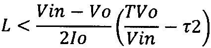
次に、第2の条件を満たすための、インダクタL1の回路定数、及び容量素子C3の回路定数について説明する。容量素子C3は、インダクタ電流ILの反転時間調整用の素子である。この容量素子C3は、図8に示すように、インダクタL1と電気的に並列に接続されることで、インダクタ電流ILの反転タイミング、つまりインダクタ電流ILの立ち上がりの開始を遅延させるように機能する。これにより、第1スイッチSW1のターンオン時において、インダクタ電流ILをゼロ以下に抑えることができ、第1スイッチSW1のソフトスイッチングを実現可能である。図8では、横軸を時間軸として、上段に第1スイッチSW1を制御する制御信号S1及び第2スイッチSW2を制御する制御信号S2を示し、下段にインダクタ電流ILを示している。制御信号S1が「H」(High Level)にあれば第1スイッチSW1がオンし、制御信号S1が「L」(Low Level)にあれば第1スイッチSW1がオフする。同様に、制御信号S2が「H」にあれば第2スイッチSW2がオンし、制御信号S2が「L」にあれば第2スイッチSW2がオフする。
Next, the circuit constant of the inductor L1 and the circuit constant of the capacitive element C3 for satisfying the second condition will be described. The capacitive element C3 is an element for adjusting the inversion time of the inductor current IL. As shown in FIG. 8, the capacitive element C3 is electrically connected in parallel with the inductor L1, thereby functioning to delay the inversion timing of the inductor current IL, that is, the start of rising of the inductor current IL. Thereby, when the first switch SW1 is turned on, the inductor current IL can be suppressed to zero or less, and soft switching of the first switch SW1 can be realized. In FIG. 8, with the horizontal axis as the time axis, the control signal S1 for controlling the first switch SW1 and the control signal S2 for controlling the second switch SW2 are shown in the upper stage, and the inductor current IL is shown in the lower stage. If the control signal S1 is “H” (HighSLevel), the first switch SW1 is turned on. If the control signal S1 is “L” (Low Level), the first switch SW1 is turned off. Similarly, when the control signal S2 is “H”, the second switch SW2 is turned on, and when the control signal S2 is “L”, the second switch SW2 is turned off.
ここで、容量素子C3に蓄積される電気エネルギが、インダクタL1の電気エネルギより十分に小さい場合において、図8の期間τ1,τ2に容量素子C3から放電される電荷量は、それぞれ下記数6,7の式で表される。図8においては、斜線領域が容量素子C3から放電される電気エネルギを表している。
Here, when the electrical energy stored in the capacitive element C3 is sufficiently smaller than the electrical energy of the inductor L1, the amount of charge discharged from the capacitive element C3 during the periods τ1 and τ2 in FIG. 7 In FIG. 8, the shaded area represents the electrical energy discharged from the capacitive element C3.
ここで、「C」は容量素子C3の容量値であって、「D」は第1スイッチSW1のデューティ比である。そのため、上記式中の「DT」はオン時間TonにデッドタイムTdを加えた値となり、「DT-τ2」はインダクタ電流ILが上昇する期間に相当する。ここで、第2の条件を満たすためには、デッドタイムTd内に、インダクタ電流ILの反転を完了する必要がある。すなわち、数6,7の式において、「τ1<Td」及び「τ2<Td」の関係を満たすように、インダクタL1のインダクタンスL、及び容量素子C3の容量値Cが設定される必要がある。要するに、数6,7の式にて「τ1<Td」及び「τ2<Td」の条件を満足する範囲に、インダクタンスL及び容量値Cが設定されていれば、第2の条件を満たすことになる。
Here, “C” is the capacitance value of the capacitive element C3, and “D” is the duty ratio of the first switch SW1. Therefore, “DT” in the above formula is a value obtained by adding the dead time Td to the on time Ton, and “DT−τ2” corresponds to a period during which the inductor current IL increases. Here, in order to satisfy the second condition, inversion of the inductor current IL needs to be completed within the dead time Td. That is, in the equations 6 and 7, it is necessary to set the inductance L of the inductor L1 and the capacitance value C of the capacitive element C3 so as to satisfy the relationship of “τ1 <Td” and “τ2 <Td”. In short, if the inductance L and the capacitance value C are set in a range that satisfies the conditions of “τ1 <Td” and “τ2 <Td” in the expressions 6 and 7, the second condition is satisfied. Become.
ところで、ここではスナバ回路3における第1スイッチSW1及び第2スイッチSW2のうち、第1スイッチSW1についてソフトスイッチングの説明をしたが、第2スイッチSW2についても同様にソフトスイッチングが実現可能である。
By the way, although soft switching was demonstrated about 1st switch SW1 among 1st switch SW1 and 2nd switch SW2 in snubber circuit 3 here, soft switching is similarly realizable also about 2nd switch SW2.
(3.4)スナバ回路の動作シーケンス
以下、スナバ回路3の動作シーケンスについて、図9~図12Cを参照して、さらに詳しく説明する。以下の説明では、スナバ回路3の各部の電圧及び電流を、図10に示す矢印の通り定義する。電圧又は電流の極性(正/負)についても、図10に矢印で示す向きを、電圧又は電流の「正」の向きと定義する。図11A~図12Cでは、スナバ回路3の動作の説明のため、各フェーズにおけるスナバ回路3の動作を反映した等価回路を示している。 (3.4) Operation Sequence of Snubber Circuit Hereinafter, the operation sequence of the snubber circuit 3 will be described in more detail with reference to FIGS. 9 to 12C. In the following description, the voltage and current of each part of the snubber circuit 3 are defined as shown by arrows in FIG. Regarding the polarity (positive / negative) of voltage or current, the direction indicated by the arrow in FIG. 10 is defined as the “positive” direction of voltage or current. 11A to 12C show an equivalent circuit reflecting the operation of the snubber circuit 3 in each phase for explaining the operation of the snubber circuit 3. FIG.
以下、スナバ回路3の動作シーケンスについて、図9~図12Cを参照して、さらに詳しく説明する。以下の説明では、スナバ回路3の各部の電圧及び電流を、図10に示す矢印の通り定義する。電圧又は電流の極性(正/負)についても、図10に矢印で示す向きを、電圧又は電流の「正」の向きと定義する。図11A~図12Cでは、スナバ回路3の動作の説明のため、各フェーズにおけるスナバ回路3の動作を反映した等価回路を示している。 (3.4) Operation Sequence of Snubber Circuit Hereinafter, the operation sequence of the snubber circuit 3 will be described in more detail with reference to FIGS. 9 to 12C. In the following description, the voltage and current of each part of the snubber circuit 3 are defined as shown by arrows in FIG. Regarding the polarity (positive / negative) of voltage or current, the direction indicated by the arrow in FIG. 10 is defined as the “positive” direction of voltage or current. 11A to 12C show an equivalent circuit reflecting the operation of the snubber circuit 3 in each phase for explaining the operation of the snubber circuit 3. FIG.
スナバ回路3の動作は、図9に示すように、第1フェーズM1~第7フェーズM7の7つのフェーズに区分できる。図9では、横軸を時間軸として、最上段に制御信号S1及び制御信号S2、2段目にスイッチ電流Isw1及びスイッチ電圧Vsw1、3段目にスイッチ電流Isw2及びスイッチ電圧Vsw2を示している。更に、4段目にインダクタL1の両端電圧(以下、「インダクタ電圧VL」という)、5段目にインダクタ電流IL、6段目に負荷電流Io、7段目には、第3容量素子C3に流れる電流Ic3を示している。更に、8段目には、第2容量素子C2に流れる電流Ic2及びインダクタ電流IL、最下段に第2クランプ電圧Vc2及びスイッチ電圧Vsw2を示している。ここでは、第1スイッチSW1と第2スイッチSW2とでオン時間の長さが異なるように、制御信号S1と制御信号S2とは非対称の信号波形とし、制御信号S1,S2のデューティ比は固定値とする。
The operation of the snubber circuit 3 can be divided into seven phases of the first phase M1 to the seventh phase M7 as shown in FIG. In FIG. 9, with the horizontal axis as the time axis, the control signal S1 and control signal S2 are shown in the uppermost stage, the switch current Isw1 and the switch voltage Vsw1 in the second stage, and the switch current Isw2 and the switch voltage Vsw2 in the third stage. Further, the voltage across the inductor L1 in the fourth stage (hereinafter referred to as “inductor voltage VL”), the inductor current IL in the fifth stage, the load current Io in the sixth stage, and the third capacitor element C3 in the seventh stage. A flowing current Ic3 is shown. Further, in the eighth stage, the current Ic2 and the inductor current IL flowing through the second capacitive element C2 are shown, and the second clamp voltage Vc2 and the switch voltage Vsw2 are shown in the lowest stage. Here, the control signal S1 and the control signal S2 are asymmetrical signal waveforms so that the length of the on-time differs between the first switch SW1 and the second switch SW2, and the duty ratio of the control signals S1 and S2 is a fixed value. And
まず、第1フェーズM1においては、第1スイッチSW1がオン、第2スイッチSW2がオフであるため、スナバ回路3は、等価的に図11Aに示すような動作状態になる。この期間において、第2容量素子C2の容量値が十分に大きく、負荷電流Ioが直流電流であれば、インダクタ電圧VLは、一定電圧となり、第1クランプ値v1と第2クランプ値v2との差分値(v1-v2)を維持する。一方、インダクタ電流ILは線形増加する。このときのスイッチ電流Isw1は、インダクタ電流ILと同一である。このとき、第2容量素子C2は、インダクタ電流ILから負荷電流Ioを差し引いた電流Ic2(=IL-Io)にて充電される。
First, in the first phase M1, since the first switch SW1 is on and the second switch SW2 is off, the snubber circuit 3 is equivalently in an operation state as shown in FIG. 11A. In this period, if the capacitance value of the second capacitive element C2 is sufficiently large and the load current Io is a direct current, the inductor voltage VL becomes a constant voltage, and the difference between the first clamp value v1 and the second clamp value v2 The value (v1-v2) is maintained. On the other hand, the inductor current IL increases linearly. The switch current Isw1 at this time is the same as the inductor current IL. At this time, the second capacitive element C2 is charged with a current Ic2 (= IL-Io) obtained by subtracting the load current Io from the inductor current IL.
第2フェーズM2においては、第1スイッチSW1がターンオフし、第2スイッチSW2がオフを維持することでデッドタイムTdに移行するため、スナバ回路3は、等価的に図11Bに示すような動作状態になる。この期間において、インダクタL1及び第3容量素子C3は、一対の第1電圧点P11,P12及び一対の第2電圧点P21,P22から電気的に切り離され、LC並列共振回路を構成する。ここで、第3容量素子C3が放電することにより、電流Ic3が図11Bに矢印で示す向きに流れ、インダクタ電圧VLの向き(極性)が次第に反転する。このとき、電流Ic3はインダクタ電流ILと同一であって、負荷電流Ioは電流Ic2と同一である。ここで、第3容量素子C3がスイッチ電圧Vsw1の立ち上がりを遅延させることにより、スイッチ電圧Vsw1とスイッチ電流Isw1との重複が回避され、ソフトスイッチングが実現される。
In the second phase M2, since the first switch SW1 is turned off and the second switch SW2 is kept off to shift to the dead time Td, the snubber circuit 3 is equivalent to an operation state as shown in FIG. 11B. become. During this period, the inductor L1 and the third capacitive element C3 are electrically disconnected from the pair of first voltage points P11 and P12 and the pair of second voltage points P21 and P22, thereby forming an LC parallel resonance circuit. Here, as the third capacitive element C3 is discharged, the current Ic3 flows in the direction indicated by the arrow in FIG. 11B, and the direction (polarity) of the inductor voltage VL is gradually reversed. At this time, the current Ic3 is the same as the inductor current IL, and the load current Io is the same as the current Ic2. Here, the third capacitor C3 delays the rise of the switch voltage Vsw1, thereby avoiding the overlap between the switch voltage Vsw1 and the switch current Isw1, and realizing soft switching.
第3フェーズM3は、インダクタ電圧VLの向き(極性)の反転後のデッドタイムTdであって、第1スイッチSW1がオフを維持し、第2スイッチSW2がオフを維持し、スナバ回路3は、等価的に図11Cに示すような動作状態になる。この期間においては、第2スイッチSW2の寄生ダイオードがオンし、この寄生ダイオードを通して、図11Cに矢印で示す向きに還流電流が流れる。インダクタ電圧VLは、一定電圧となり、第2クランプ電圧Vc2と同値を維持する。このとき、第3容量素子C3の充放電は行われない。この期間においては、インダクタ電流ILが、負荷電流Ioと電流Ic2との合計で表され(IL=Io+Ic2)、インダクタ電流ILの直流成分が負荷電流Io、リップル成分が電流Ic2となる。この期間において、スイッチ電圧Vsw1は最大値(第1クランプ値v1)まで立ち上がる。
The third phase M3 is a dead time Td after inversion of the direction (polarity) of the inductor voltage VL, the first switch SW1 is kept off, the second switch SW2 is kept off, and the snubber circuit 3 is Equivalently, the operation state as shown in FIG. 11C is obtained. During this period, the parasitic diode of the second switch SW2 is turned on, and a reflux current flows through the parasitic diode in the direction indicated by the arrow in FIG. 11C. The inductor voltage VL is a constant voltage and maintains the same value as the second clamp voltage Vc2. At this time, charging / discharging of the 3rd capacitive element C3 is not performed. In this period, the inductor current IL is represented by the sum of the load current Io and the current Ic2 (IL = Io + Ic2), and the DC component of the inductor current IL is the load current Io and the ripple component is the current Ic2. In this period, the switch voltage Vsw1 rises to the maximum value (first clamp value v1).
第4フェーズM4においては、第1スイッチSW1がオフを維持し、第2スイッチSW2がターンオンするため、スナバ回路3は、等価的に図11Dに示すような動作状態になる。この期間においても暫くは、第3フェーズM3と同様に、第2スイッチSW2を還流電流が流れる。この期間の途中で、スイッチ電流Isw2、インダクタ電流IL、及び電流Ic2の極性が反転する。つまり、スイッチ電流Isw2は負から正へ、インダクタ電流ILは正から負へ、電流Ic2は正から負へ変化する。インダクタ電流ILが負になると、第2容量素子C2の放電が開始する。
In the fourth phase M4, since the first switch SW1 is kept off and the second switch SW2 is turned on, the snubber circuit 3 is equivalently in an operation state as shown in FIG. 11D. Even during this period, a reflux current flows through the second switch SW2 for a while as in the third phase M3. In the middle of this period, the polarities of the switch current Isw2, the inductor current IL, and the current Ic2 are reversed. That is, the switch current Isw2 changes from negative to positive, the inductor current IL changes from positive to negative, and the current Ic2 changes from positive to negative. When the inductor current IL becomes negative, the discharge of the second capacitor element C2 starts.
第5フェーズM5においては、第1スイッチSW1がオフを維持し、第2スイッチSW2がターンオフすることでデッドタイムTdに移行するため、スナバ回路3は、等価的に図12Aに示すような動作状態になる。この期間においては、第2フェーズM2と同様に、インダクタL1及び第3容量素子C3は、一対の第1電圧点P11,P12及び一対の第2電圧点P21,P22から電気的に切り離され、LC並列共振回路を構成する。ここで、第3容量素子C3が放電することにより、電流Ic3が図12Aに矢印で示す向きに流れ、インダクタ電圧VLの向き(極性)が次第に反転する。このとき、電流Ic3はインダクタ電流ILと同一であって、負荷電流Ioは電流Ic2と同一である。
In the fifth phase M5, since the first switch SW1 is kept off and the second switch SW2 is turned off to shift to the dead time Td, the snubber circuit 3 is equivalently operated as shown in FIG. 12A. become. During this period, similarly to the second phase M2, the inductor L1 and the third capacitive element C3 are electrically disconnected from the pair of first voltage points P11 and P12 and the pair of second voltage points P21 and P22, and the LC A parallel resonant circuit is configured. Here, as the third capacitive element C3 is discharged, the current Ic3 flows in the direction indicated by the arrow in FIG. 12A, and the direction (polarity) of the inductor voltage VL is gradually reversed. At this time, the current Ic3 is the same as the inductor current IL, and the load current Io is the same as the current Ic2.
第6フェーズM6は、インダクタ電圧VLの向き(極性)の反転後のデッドタイムTdであって、第1スイッチSW1がオフを維持し、第2スイッチSW2がオフを維持し、スナバ回路3は、等価的に図12Bに示すような動作状態になる。この期間においては、第1スイッチSW1の寄生ダイオードがオンし、この寄生ダイオードを通して、インダクタ電流ILが第1容量素子C1に回生される。
The sixth phase M6 is a dead time Td after inversion of the direction (polarity) of the inductor voltage VL, the first switch SW1 is kept off, the second switch SW2 is kept off, and the snubber circuit 3 is Equivalently, the operating state is as shown in FIG. 12B. During this period, the parasitic diode of the first switch SW1 is turned on, and the inductor current IL is regenerated to the first capacitor element C1 through the parasitic diode.
第7フェーズM7においては、第1スイッチSW1がターンオンし、第2スイッチSW2がオフを維持するため、スナバ回路3は、等価的に図12Cに示すような動作状態になる。この期間において、スイッチ電流Isw1がインダクタ電流ILと同一になるが、第6フェーズM6に引き続き、インダクタ電流ILが第1容量素子C1に回生される。このとき、スイッチ電流Isw1の極性は負であり、スイッチ電圧Vsw1の立ち下がり時には第1スイッチSW1の寄生ダイオードが導通しているため、スイッチング損失が低減される。
In the seventh phase M7, since the first switch SW1 is turned on and the second switch SW2 is kept off, the snubber circuit 3 is equivalently operated as shown in FIG. 12C. In this period, the switch current Isw1 becomes the same as the inductor current IL, but the inductor current IL is regenerated in the first capacitor element C1 following the sixth phase M6. At this time, the polarity of the switch current Isw1 is negative, and the switching loss is reduced because the parasitic diode of the first switch SW1 is conducting when the switch voltage Vsw1 falls.
(4)変形例
上記実施形態は本開示の一例に過ぎず、本開示は、上記実施形態に限定されることはなく、上記実施形態以外であっても、本開示に係る技術的思想を逸脱しない範囲であれば、設計等に応じて種々の変更が可能である。以下、上記実施形態の変形例を列挙する。 (4) Modifications The above embodiment is merely an example of the present disclosure, and the present disclosure is not limited to the above embodiment, and deviates from the technical idea according to the present disclosure even in other embodiments. Various changes can be made in accordance with the design or the like as long as they are not. Hereinafter, modifications of the embodiment will be listed.
上記実施形態は本開示の一例に過ぎず、本開示は、上記実施形態に限定されることはなく、上記実施形態以外であっても、本開示に係る技術的思想を逸脱しない範囲であれば、設計等に応じて種々の変更が可能である。以下、上記実施形態の変形例を列挙する。 (4) Modifications The above embodiment is merely an example of the present disclosure, and the present disclosure is not limited to the above embodiment, and deviates from the technical idea according to the present disclosure even in other embodiments. Various changes can be made in accordance with the design or the like as long as they are not. Hereinafter, modifications of the embodiment will be listed.
電力変換システム1及び蓄電池5を含む蓄電システムは、非住宅施設に限らず、例えば、住宅に導入されてもよいし、電気自動車等、施設以外に適用されてもよい。また、電力変換システム1は、電力系統4と、蓄電池5との間における電力変換に限らず、例えば、太陽光発電装置又は燃料電池等の発電設備と、電力系統4又は負荷との間の電力変換に用いられてもよい。
The power storage system including the power conversion system 1 and the storage battery 5 is not limited to a non-residential facility, and may be introduced into a house, or may be applied to a facility other than a facility such as an electric vehicle. Moreover, the power conversion system 1 is not limited to power conversion between the power system 4 and the storage battery 5, for example, power between a power generation facility such as a solar power generation device or a fuel cell, and the power system 4 or a load. It may be used for conversion.
また、電力変換システム1は、双方向に電力の変換を行う構成に限らず、例えば、一対の一次側端子T11,T12から一対の二次側端子T21,T22への一方向にのみ、電力の変換を行う構成であってもよい。
In addition, the power conversion system 1 is not limited to a configuration that performs power conversion in both directions. For example, the power conversion system 1 can transmit power only in one direction from the pair of primary terminals T11 and T12 to the pair of secondary terminals T21 and T22. The structure which performs conversion may be sufficient.
また、スナバ回路3の電圧変換回路33において、第2スイッチSW2は、MOSFETに限らず、例えば、ダイオードであってもよい。この場合、第2スイッチSW2は、MOSFETの寄生ダイオードと同じ向き、つまり、カソードが第1スイッチSW1のソースに接続され、アノードが低電位側の第1電圧点P12に接続されるように設けられる。
Further, in the voltage conversion circuit 33 of the snubber circuit 3, the second switch SW2 is not limited to the MOSFET but may be a diode, for example. In this case, the second switch SW2 is provided in the same direction as the parasitic diode of the MOSFET, that is, the cathode is connected to the source of the first switch SW1 and the anode is connected to the first voltage point P12 on the low potential side. .
また、第1クランプ回路31が主回路2の一対の第1電圧点P11,P12から吸収した電気エネルギを、第2クランプ回路32は、一対の第1電圧点P11,P12とは電気的に異なる位置から主回路2に回生してもよい。この場合、電圧変換回路33は、第1クランプ電圧Vc1を降圧して第2クランプ電圧Vc2を生成する降圧回路に限らず、例えば、第1クランプ電圧Vc1を昇圧して第2クランプ電圧Vc2を生成する昇圧回路であってもよい。
Further, the second clamp circuit 32 is electrically different from the pair of first voltage points P11 and P12 in the electrical energy absorbed by the first clamp circuit 31 from the pair of first voltage points P11 and P12 of the main circuit 2. You may regenerate to the main circuit 2 from a position. In this case, the voltage conversion circuit 33 is not limited to the step-down circuit that steps down the first clamp voltage Vc1 to generate the second clamp voltage Vc2, but for example, steps up the first clamp voltage Vc1 to generate the second clamp voltage Vc2. It may be a booster circuit.
また、容量素子C3は、インダクタL1と電気的に並列に接続されていることは必須ではなく、第1スイッチSW1とインダクタL1との少なくとも一方と電気的に並列に接続されていればよい。すなわち、容量素子C3は、第1スイッチSW1と電気的に並列に接続されていてもよいし、第1スイッチSW1及びインダクタL1の両方と電気的に並列に接続されていてもよい。
Further, it is not essential that the capacitive element C3 is electrically connected in parallel with the inductor L1, as long as it is electrically connected in parallel with at least one of the first switch SW1 and the inductor L1. That is, the capacitive element C3 may be electrically connected in parallel with the first switch SW1, or may be electrically connected in parallel with both the first switch SW1 and the inductor L1.
また、第1ダイオードD1は、上記実施形態のように、一対の第1電圧点P11,P12における高電位側の第1電圧点P11に電気的に接続される構成に限らず、低電位側の第1電圧点P12に電気的に接続されていてもよい。第2ダイオードD2についても同様に、一対の第2電圧点P21,P22における低電位側の第2電圧点P22に電気的に接続されていてもよい。更に、第1ダイオードD1及び第2ダイオードD2は、例えば、MOSFETの寄生ダイオード等であってもよい。
In addition, the first diode D1 is not limited to the configuration in which the first diode D1 is electrically connected to the first voltage point P11 on the high potential side in the pair of first voltage points P11 and P12. It may be electrically connected to the first voltage point P12. Similarly, the second diode D2 may be electrically connected to the second voltage point P22 on the low potential side in the pair of second voltage points P21 and P22. Furthermore, the first diode D1 and the second diode D2 may be, for example, MOSFET parasitic diodes.
また、第1~第8のスイッチング素子Q11~Q18の各々は、MOSFETの寄生ダイオードを有しているが、寄生ダイオードとは別に、第1~第8のスイッチング素子Q11~Q18の各々と逆並列にダイオードが電気的に接続されていてもよい。更に、第1~第8のスイッチング素子Q11~Q18の各々は、MOSFETに限らず、例えば、IGBT(Insulated Gate Bipolar Transistor)等であってもよい。
Each of the first to eighth switching elements Q11 to Q18 has a MOSFET parasitic diode, but, apart from the parasitic diode, is antiparallel to each of the first to eighth switching elements Q11 to Q18. A diode may be electrically connected. Further, each of the first to eighth switching elements Q11 to Q18 is not limited to a MOSFET, but may be, for example, an IGBT (Insulated Gate Gate Bipolar Transistor) or the like.
また、RCスナバ23は電力変換システム1(主回路2)に必須の構成ではなく、RCスナバ23は適宜省略されてもよい。
Further, the RC snubber 23 is not an essential component for the power conversion system 1 (main circuit 2), and the RC snubber 23 may be omitted as appropriate.
また、第1クランプ電圧Vc1は、第1クランプ値v1を規定する電圧であればよく、第1クランプ電圧Vc1の大きさが第1クランプ値v1であることは必須ではなく、例えば、第1クランプ電圧Vc1を分圧した電圧の大きさを第1クランプ値v1としてもよい。第2クランプ電圧Vc2についても同様に、第2クランプ値v2を規定する電圧であればよい。
The first clamp voltage Vc1 may be a voltage that defines the first clamp value v1, and it is not essential that the magnitude of the first clamp voltage Vc1 is the first clamp value v1, for example, the first clamp voltage Vc1 The magnitude of the voltage obtained by dividing the voltage Vc1 may be set as the first clamp value v1. Similarly, the second clamp voltage Vc2 may be a voltage that defines the second clamp value v2.
また、上記実施形態では、電力系統4が単相交流について説明したが、この構成に限らず、電力系統4は、例えば、三相交流であってもよい。三相交流の場合、主回路2は、3つの一次側端子と3つの二次側端子とを有することが好ましい。
In the above-described embodiment, the power system 4 has been described with respect to single-phase AC. However, the configuration is not limited to this configuration, and the power system 4 may be, for example, three-phase AC. In the case of three-phase alternating current, the main circuit 2 preferably has three primary terminals and three secondary terminals.
(5)まとめ
以上説明したように、第1の態様に係るスナバ回路3は、第1クランプ回路31と、第2クランプ回路32と、電圧変換回路33と、を備える。第1クランプ回路31は、主回路2における一対の第1電圧点P11,P12間の電圧の大きさが第1クランプ値v1を超える場合に、一対の第1電圧点P11,P12点から主回路2の電気エネルギを吸収する。これにより、第1クランプ回路31は、一対の第1電圧点P11,P12間の電圧を第1クランプ値v1にクランプする。第2クランプ回路32は、主回路2における一対の第2電圧点P21,P22間の電圧の大きさが第2クランプ値v2を下回る場合に、一対の第2電圧点P21,P22から主回路2に電気エネルギを注入する。これにより、第2クランプ回路32は、一対の第2電圧点P21,P22間の電圧を第2クランプ値v2にクランプする。電圧変換回路33は、第1クランプ回路31及び第2クランプ回路32に電気的に接続され、第1クランプ値v1を規定する第1クランプ電圧Vc1と第2クランプ値v2を規定する第2クランプ電圧Vc2との間で電圧変換を行う。 (5) Summary As described above, the snubber circuit 3 according to the first aspect includes thefirst clamp circuit 31, the second clamp circuit 32, and the voltage conversion circuit 33. The first clamp circuit 31 starts from the pair of first voltage points P11 and P12 when the magnitude of the voltage between the pair of first voltage points P11 and P12 in the main circuit 2 exceeds the first clamp value v1. 2 electrical energy is absorbed. Thereby, the first clamp circuit 31 clamps the voltage between the pair of first voltage points P11 and P12 to the first clamp value v1. When the magnitude of the voltage between the pair of second voltage points P21 and P22 in the main circuit 2 is lower than the second clamp value v2, the second clamp circuit 32 is connected to the main circuit 2 from the pair of second voltage points P21 and P22. Inject electrical energy into Thus, the second clamp circuit 32 clamps the voltage between the pair of second voltage points P21 and P22 to the second clamp value v2. The voltage conversion circuit 33 is electrically connected to the first clamp circuit 31 and the second clamp circuit 32, and the first clamp voltage Vc1 that defines the first clamp value v1 and the second clamp voltage that defines the second clamp value v2. Voltage conversion is performed with Vc2.
以上説明したように、第1の態様に係るスナバ回路3は、第1クランプ回路31と、第2クランプ回路32と、電圧変換回路33と、を備える。第1クランプ回路31は、主回路2における一対の第1電圧点P11,P12間の電圧の大きさが第1クランプ値v1を超える場合に、一対の第1電圧点P11,P12点から主回路2の電気エネルギを吸収する。これにより、第1クランプ回路31は、一対の第1電圧点P11,P12間の電圧を第1クランプ値v1にクランプする。第2クランプ回路32は、主回路2における一対の第2電圧点P21,P22間の電圧の大きさが第2クランプ値v2を下回る場合に、一対の第2電圧点P21,P22から主回路2に電気エネルギを注入する。これにより、第2クランプ回路32は、一対の第2電圧点P21,P22間の電圧を第2クランプ値v2にクランプする。電圧変換回路33は、第1クランプ回路31及び第2クランプ回路32に電気的に接続され、第1クランプ値v1を規定する第1クランプ電圧Vc1と第2クランプ値v2を規定する第2クランプ電圧Vc2との間で電圧変換を行う。 (5) Summary As described above, the snubber circuit 3 according to the first aspect includes the
この構成によれば、スナバ回路3は、一対の第1電圧点P11,P12間の電圧(Vbus)に正のリンギングが生じた場合、第1クランプ回路31にて、主回路2の電気エネルギを吸収することにより、バス電圧Vbusを第1クランプ値v1にクランプする。また、スナバ回路3は、一対の第2電圧点P21,P22間の電圧(Vbus)に負のリンギングが生じた場合、第2クランプ回路32にて、主回路2に電気エネルギを注入することにより、バス電圧Vbusを第2クランプ値v2にクランプする。しかも、第1クランプ値v1を規定する第1クランプ電圧Vc1と第2クランプ値v2を規定する第2クランプ電圧Vc2との間では、電圧変換回路33による電圧変換が行われる。すなわち、スナバ回路3は、正のリンギングが生じた際に第1クランプ回路31が主回路2から吸収した電気エネルギを、負のリンギングが生じた際に第2クランプ回路32から主回路2に回生している。したがって、スナバ回路3においては、吸収したエネルギを熱に変換して消費するRCDスナバ回路に比較して、電気エネルギが有効に利用され、スナバ回路3での損失を小さく抑えることができる。
According to this configuration, the snubber circuit 3 generates the electric energy of the main circuit 2 in the first clamp circuit 31 when positive ringing occurs in the voltage (Vbus) between the pair of first voltage points P11 and P12. By absorbing, the bus voltage Vbus is clamped to the first clamp value v1. Further, the snubber circuit 3 causes the second clamp circuit 32 to inject electric energy into the main circuit 2 when negative ringing occurs in the voltage (Vbus) between the pair of second voltage points P21 and P22. The bus voltage Vbus is clamped to the second clamp value v2. In addition, voltage conversion by the voltage conversion circuit 33 is performed between the first clamp voltage Vc1 that defines the first clamp value v1 and the second clamp voltage Vc2 that defines the second clamp value v2. That is, the snubber circuit 3 regenerates electric energy absorbed from the main circuit 2 by the first clamp circuit 31 when positive ringing occurs from the second clamp circuit 32 to the main circuit 2 when negative ringing occurs. is doing. Therefore, in the snubber circuit 3, electric energy is used more effectively than in the RCD snubber circuit that converts the absorbed energy into heat and is consumed, and the loss in the snubber circuit 3 can be kept small.
しかも、スナバ回路3は、一対の第1電圧点P11,P12間の電圧が第1クランプ値v1を超えた場合、及び一対の第2電圧点P21,P22間の電圧が第2クランプ値v2を下回った場合にのみ、電気エネルギの回生を行う。したがって、スナバ回路3は、一対の第1電圧点P11,P12間、又は一対の第2電圧点P21,P22間にかかる正常な電圧(バス電圧Vbus)については回生することなく、リンギング成分のみを回生することが可能である。これにより、スナバ回路3は、主回路2の動作に与える影響を比較的小さく抑えることができる。
Moreover, the snubber circuit 3 has the second clamp value v2 when the voltage between the pair of first voltage points P11 and P12 exceeds the first clamp value v1 and the voltage between the pair of second voltage points P21 and P22. Only when it falls below, regenerates electric energy. Therefore, the snubber circuit 3 does not regenerate a normal voltage (bus voltage Vbus) applied between the pair of first voltage points P11 and P12 or between the pair of second voltage points P21 and P22, but only the ringing component. It is possible to regenerate. Thereby, the snubber circuit 3 can suppress the influence which it has on operation | movement of the main circuit 2 comparatively small.
また、非絶縁方式の電圧変換回路33を採用する場合は、スナバ回路3にはトランスが不要になり、スナバ回路3の構成の簡略化及び損失の低減を図ることができる。更に、電圧変換回路33の制御用に自律式の制御回路34を採用する場合は、スナバ回路3の回路規模を小さく抑えることができる。
Further, when the non-insulated voltage conversion circuit 33 is employed, the snubber circuit 3 does not require a transformer, and the configuration of the snubber circuit 3 can be simplified and loss can be reduced. Furthermore, when the autonomous control circuit 34 is used for controlling the voltage conversion circuit 33, the circuit scale of the snubber circuit 3 can be reduced.
第2の態様に係るスナバ回路3は、第1の態様において、一対の第1電圧点P11,P12における高電位側の第1電圧点P11と一対の第2電圧点P21,P22における高電位側の第2電圧点P21とが同電位であることが好ましい。この場合、一対の第1電圧点P11,P12における低電位側の第1電圧点P12と一対の第2電圧点P21,P22における低電位側の第2電圧点P22とは同電位であることが好ましい。電圧変換回路33は、第1クランプ電圧Vc1を降圧して第2クランプ電圧Vc2を生成するように構成されていることが好ましい。この構成によれば、第1クランプ回路31が主回路2の一対の第1電圧点P11,P12から吸収した電気エネルギを、第2クランプ回路32は、一対の第1電圧点P11,P12と電気的に等価な位置から主回路2に回生できる。したがって、スナバ回路3は、双方向に電力の変換を行う主回路2に適用可能である。
In the first aspect, the snubber circuit 3 according to the second aspect includes a first voltage point P11 on the high potential side at the pair of first voltage points P11 and P12 and a high potential side at the pair of second voltage points P21 and P22. The second voltage point P21 is preferably at the same potential. In this case, the first voltage point P12 on the low potential side of the pair of first voltage points P11 and P12 and the second voltage point P22 on the low potential side of the pair of second voltage points P21 and P22 may have the same potential. preferable. The voltage conversion circuit 33 is preferably configured to step down the first clamp voltage Vc1 and generate the second clamp voltage Vc2. According to this configuration, the second clamp circuit 32 is electrically connected to the pair of first voltage points P11 and P12 using the electric energy absorbed by the first clamp circuit 31 from the pair of first voltage points P11 and P12 of the main circuit 2. Therefore, the main circuit 2 can be regenerated from an equivalent position. Accordingly, the snubber circuit 3 can be applied to the main circuit 2 that performs bidirectional power conversion.
第3の態様に係るスナバ回路3は、第1又は2の態様において、電圧変換回路33が、半導体スイッチ(第1スイッチSW1)と、インダクタL1と、容量素子C3と、を有するDC/DCコンバータであることが好ましい。この場合、容量素子C3は、半導体スイッチとインダクタL1との少なくとも一方と電気的に並列に接続されることが好ましい。この構成によれば、電圧変換回路33における半導体スイッチのソフトスイッチングを実現可能であって、スナバ回路3内で生じるリンギング及び損失を小さく抑えることができる。ただし、この構成はスナバ回路3に必須の構成ではなく、容量素子C3は適宜省略可能である。
The snubber circuit 3 according to a third aspect is the DC / DC converter according to the first or second aspect, in which the voltage conversion circuit 33 includes a semiconductor switch (first switch SW1), an inductor L1, and a capacitive element C3. It is preferable that In this case, it is preferable that the capacitive element C3 is electrically connected in parallel with at least one of the semiconductor switch and the inductor L1. According to this configuration, soft switching of the semiconductor switch in the voltage conversion circuit 33 can be realized, and ringing and loss generated in the snubber circuit 3 can be suppressed to be small. However, this configuration is not essential for the snubber circuit 3, and the capacitive element C3 can be omitted as appropriate.
第4の態様に係るスナバ回路3は、第1~3のいずれかの態様において、第1クランプ回路31が、一対の第1電圧点P11,P12間に電気的に直列に接続された第1ダイオードD1及び第1容量素子C1を有することが好ましい。この場合、第1クランプ回路31は、一対の第1電圧点P11,P12間の電圧が第1クランプ値v1を超える場合に、主回路2から第1ダイオードD1を通して第1容量素子C1に電流が流れるように構成されていることが好ましい。第2クランプ回路32は、一対の第2電圧点P21,P22間に電気的に直列に接続された第2ダイオードD2及び第2容量素子C2を有することが好ましい。この場合、第2クランプ回路32は、一対の第2電圧点P21,P22間の電圧が第2クランプ値v2を下回る場合に、第2容量素子C2から第2ダイオードD2を通して主回路2に電流が流れるように構成されていることが好ましい。この構成によれば、ダイオード及び容量素子(コンデンサ等)を用いた比較的簡単な回路構成により、第1クランプ回路31及び第2クランプ回路32が実現される。
In the snubber circuit 3 according to the fourth aspect, in any one of the first to third aspects, the first clamp circuit 31 is electrically connected in series between the pair of first voltage points P11 and P12. It is preferable to have a diode D1 and a first capacitor element C1. In this case, when the voltage between the pair of first voltage points P11 and P12 exceeds the first clamp value v1, the first clamp circuit 31 causes a current to flow from the main circuit 2 to the first capacitive element C1 through the first diode D1. It is preferably configured to flow. The second clamp circuit 32 preferably includes a second diode D2 and a second capacitor element C2 that are electrically connected in series between the pair of second voltage points P21 and P22. In this case, when the voltage between the pair of second voltage points P21 and P22 is lower than the second clamp value v2, the second clamp circuit 32 causes a current to flow from the second capacitance element C2 to the main circuit 2 through the second diode D2. It is preferably configured to flow. According to this configuration, the first clamp circuit 31 and the second clamp circuit 32 are realized by a relatively simple circuit configuration using a diode and a capacitive element (a capacitor or the like).
第5の態様に係るスナバ回路3は、第1~4のいずれかの態様において、電圧変換回路33が、半導体スイッチ(第1スイッチSW1)と、インダクタL1と、を有するDC/DCコンバータであることが好ましい。この場合、電圧変換回路33は、インダクタL1を流れるインダクタ電流ILが不連続モードとなるように半導体スイッチをスイッチング動作させるように構成されていることが好ましい。この構成によれば、電圧変換回路33における半導体スイッチのソフトスイッチングを実現可能であって、スナバ回路3内で生じるリンギング及び損失を小さく抑えることができる。ただし、この構成はスナバ回路3に必須の構成ではなく、電圧変換回路33は、インダクタL1を流れるインダクタ電流ILが臨界モード又は連続モードとなるように半導体スイッチをスイッチング動作させてもよい。
The snubber circuit 3 according to the fifth aspect is a DC / DC converter according to any one of the first to fourth aspects, wherein the voltage conversion circuit 33 includes a semiconductor switch (first switch SW1) and an inductor L1. It is preferable. In this case, the voltage conversion circuit 33 is preferably configured to switch the semiconductor switch so that the inductor current IL flowing through the inductor L1 is in the discontinuous mode. According to this configuration, soft switching of the semiconductor switch in the voltage conversion circuit 33 can be realized, and ringing and loss generated in the snubber circuit 3 can be suppressed to be small. However, this configuration is not essential for the snubber circuit 3, and the voltage conversion circuit 33 may switch the semiconductor switch so that the inductor current IL flowing through the inductor L1 is in a critical mode or a continuous mode.
第6の態様に係るスナバ回路3は、第1~5のいずれかの態様において、電圧変換回路33が、半導体スイッチ(第1スイッチSW1)と、インダクタL1と、半導体スイッチを制御する制御回路34と、を有するDC/DCコンバータであることが好ましい。この場合、制御回路34は、半導体スイッチのデューティ比を調節することによって、第1クランプ値v1及び第2クランプ値v2を調節するように構成されていることが好ましい。この構成によれば、半導体スイッチのデューティ比の調節により、第1クランプ値v1及び第2クランプ値v2を任意の値に設定可能となる。ただし、この構成はスナバ回路3に必須の構成ではなく、半導体スイッチのデューティ比は固定であってもよい。
In the snubber circuit 3 according to the sixth aspect, in any one of the first to fifth aspects, the voltage conversion circuit 33 controls the semiconductor switch (first switch SW1), the inductor L1, and the semiconductor switch. It is preferable that the DC / DC converter has In this case, it is preferable that the control circuit 34 is configured to adjust the first clamp value v1 and the second clamp value v2 by adjusting the duty ratio of the semiconductor switch. According to this configuration, the first clamp value v1 and the second clamp value v2 can be set to arbitrary values by adjusting the duty ratio of the semiconductor switch. However, this configuration is not essential for the snubber circuit 3, and the duty ratio of the semiconductor switch may be fixed.
第7の態様に係る電力変換システム1は、第1~6のいずれかの態様に係るスナバ回路3と、主回路2と、を備え、主回路2が、電力の変換を行う電力変換回路である。この構成によれば、スナバ回路3においては、RCDスナバ回路に比較して、電気エネルギが有効に利用され、スナバ回路3での損失を小さく抑えることができる。その結果、電力変換システム1におけるスナバ回路3での損失が小さく抑えられ、電力変換システム1全体としては、電力の変換効率の向上を図ることができる。特に、主回路2が比較的大電力の電力変換を行う場合には、スナバ回路3での発熱が抑えられ、スナバ回路3の小型化及び放熱構造の簡略化にもつながる。
A power conversion system 1 according to a seventh aspect includes a snubber circuit 3 according to any one of the first to sixth aspects, and a main circuit 2, and the main circuit 2 is a power conversion circuit that performs power conversion. is there. According to this configuration, compared with the RCD snubber circuit, the snubber circuit 3 can effectively use electric energy and can suppress the loss in the snubber circuit 3 to be small. As a result, the loss in the snubber circuit 3 in the power conversion system 1 can be kept small, and the power conversion system 1 as a whole can improve the power conversion efficiency. In particular, when the main circuit 2 performs power conversion with relatively high power, heat generation in the snubber circuit 3 is suppressed, leading to miniaturization of the snubber circuit 3 and simplification of the heat dissipation structure.
第8の態様に係る電力変換システム1は、第7の態様において、主回路2は、2以上の一次側端子T11,T12と2以上の二次側端子T21,T22と高周波絶縁トランス(トランス26)とを有することが好ましい。この場合、主回路2は、2以上の一次側端子T11,T12と2以上の二次側端子T21,T22との間で、高周波絶縁トランスを介して電力の変換を行うように構成されていることが好ましい。この構成によれば、電力変換システム1は、絶縁型の回路構成を採用できる。
In the power conversion system 1 according to the eighth aspect, in the seventh aspect, the main circuit 2 includes two or more primary terminals T11 and T12, two or more secondary terminals T21 and T22, and a high-frequency insulating transformer (transformer 26). ). In this case, the main circuit 2 is configured to convert power between the two or more primary terminals T11 and T12 and the two or more secondary terminals T21 and T22 via a high-frequency insulating transformer. It is preferable. According to this configuration, the power conversion system 1 can employ an insulating circuit configuration.
第9の態様に係る電力変換システム1は、第8の態様において、スナバ回路3が、高周波絶縁トランス(トランス26)に電気的に接続されていることが好ましい。この構成によれば、高周波絶縁トランスの漏れインダクタンスに起因して生じるリンギングを、スナバ回路3にて抑制することが可能である。
In the power conversion system 1 according to the ninth aspect, in the eighth aspect, it is preferable that the snubber circuit 3 is electrically connected to a high-frequency insulating transformer (transformer 26). According to this configuration, the ringing caused by the leakage inductance of the high frequency insulation transformer can be suppressed by the snubber circuit 3.
1 電力変換システム
2 主回路
26 トランス(高周波絶縁トランス)
3 スナバ回路
31 第1クランプ回路
32 第2クランプ回路
33 電圧変換回路
34 制御回路
C1 第1容量素子
C2 第2容量素子
C3 容量素子
D1 第1ダイオード
D2 第2ダイオード
L1 インダクタ
P11,P12 第1電圧点
P21,P22 第2電圧点
SW1 第1スイッチ(半導体スイッチ)
T11,T12 一次側端子
T21,T22 二次側端子
Vc1 第1クランプ電圧
v1 第1クランプ値
Vc2 第2クランプ電圧
v2 第2クランプ値 1Power Conversion System 2 Main Circuit 26 Transformer (High Frequency Insulation Transformer)
3Snubber Circuit 31 First Clamp Circuit 32 Second Clamp Circuit 33 Voltage Conversion Circuit 34 Control Circuit C1 First Capacitor C2 Second Capacitor C3 Capacitor D1 First Diode D2 Second Diode L1 Inductor P11, P12 First Voltage Point P21, P22 Second voltage point SW1 First switch (semiconductor switch)
T11, T12 Primary side terminal T21, T22 Secondary side terminal Vc1 First clamp voltage v1 First clamp value Vc2 Second clamp voltage v2 Second clamp value
2 主回路
26 トランス(高周波絶縁トランス)
3 スナバ回路
31 第1クランプ回路
32 第2クランプ回路
33 電圧変換回路
34 制御回路
C1 第1容量素子
C2 第2容量素子
C3 容量素子
D1 第1ダイオード
D2 第2ダイオード
L1 インダクタ
P11,P12 第1電圧点
P21,P22 第2電圧点
SW1 第1スイッチ(半導体スイッチ)
T11,T12 一次側端子
T21,T22 二次側端子
Vc1 第1クランプ電圧
v1 第1クランプ値
Vc2 第2クランプ電圧
v2 第2クランプ値 1
3
T11, T12 Primary side terminal T21, T22 Secondary side terminal Vc1 First clamp voltage v1 First clamp value Vc2 Second clamp voltage v2 Second clamp value
Claims (9)
- 主回路における一対の第1電圧点間の電圧の大きさが第1クランプ値を超える場合に、前記一対の第1電圧点から前記主回路の電気エネルギを吸収することによって、前記一対の第1電圧点間の電圧を前記第1クランプ値にクランプする第1クランプ回路と、
前記主回路における一対の第2電圧点間の電圧の大きさが第2クランプ値を下回る場合に、前記一対の第2電圧点から前記主回路に電気エネルギを注入することによって、前記一対の第2電圧点間の電圧を前記第2クランプ値にクランプする第2クランプ回路と、
前記第1クランプ回路及び前記第2クランプ回路に電気的に接続され、前記第1クランプ値を規定する第1クランプ電圧と前記第2クランプ値を規定する第2クランプ電圧との間で電圧変換を行う電圧変換回路と、を備える
スナバ回路。 When the magnitude of the voltage between the pair of first voltage points in the main circuit exceeds the first clamp value, the electric energy of the main circuit is absorbed from the pair of first voltage points, thereby the pair of first voltage points. A first clamp circuit for clamping a voltage between voltage points to the first clamp value;
When the magnitude of the voltage between the pair of second voltage points in the main circuit is lower than a second clamp value, electric energy is injected into the main circuit from the pair of second voltage points. A second clamp circuit for clamping a voltage between two voltage points to the second clamp value;
Voltage conversion is performed between a first clamp voltage that is electrically connected to the first clamp circuit and the second clamp circuit and that defines the first clamp value and a second clamp voltage that defines the second clamp value. A snubber circuit comprising: a voltage conversion circuit to perform; - 前記一対の第1電圧点における高電位側の第1電圧点と前記一対の第2電圧点における高電位側の第2電圧点とは同電位であり、
前記一対の第1電圧点における低電位側の第1電圧点と前記一対の第2電圧点における低電位側の第2電圧点とは同電位であり、
前記電圧変換回路は、前記第1クランプ電圧を降圧して前記第2クランプ電圧を生成するように構成されている
請求項1に記載のスナバ回路。 The first voltage point on the high potential side of the pair of first voltage points and the second voltage point on the high potential side of the pair of second voltage points are at the same potential,
The first voltage point on the low potential side of the pair of first voltage points and the second voltage point on the low potential side of the pair of second voltage points are at the same potential,
The snubber circuit according to claim 1, wherein the voltage conversion circuit is configured to step down the first clamp voltage to generate the second clamp voltage. - 前記電圧変換回路は、
半導体スイッチと、
インダクタと、
前記半導体スイッチと前記インダクタとの少なくとも一方と電気的に並列に接続された容量素子と、を有するDC/DCコンバータである
請求項1又は2に記載のスナバ回路。 The voltage conversion circuit includes:
A semiconductor switch;
An inductor;
3. The snubber circuit according to claim 1, wherein the snubber circuit is a DC / DC converter including a capacitive element electrically connected in parallel with at least one of the semiconductor switch and the inductor. - 前記第1クランプ回路は、前記一対の第1電圧点間に電気的に直列に接続された第1ダイオード及び第1容量素子を有し、前記一対の第1電圧点間の電圧が前記第1クランプ値を超える場合に、前記主回路から前記第1ダイオードを通して前記第1容量素子に電流が流れるように構成されており、
前記第2クランプ回路は、前記一対の第2電圧点間に電気的に直列に接続された第2ダイオード及び第2容量素子を有し、前記一対の第2電圧点間の電圧が前記第2クランプ値を下回る場合に、前記第2容量素子から前記第2ダイオードを通して前記主回路に電流が流れるように構成されている
請求項1~3のいずれか1項に記載のスナバ回路。 The first clamp circuit includes a first diode and a first capacitor electrically connected in series between the pair of first voltage points, and a voltage between the pair of first voltage points is the first voltage point. When the clamp value is exceeded, a current flows from the main circuit through the first diode to the first capacitor element,
The second clamp circuit includes a second diode and a second capacitor electrically connected in series between the pair of second voltage points, and a voltage between the pair of second voltage points is the second voltage point. The snubber circuit according to any one of claims 1 to 3, wherein a current flows from the second capacitive element to the main circuit through the second diode when the value is lower than a clamp value. - 前記電圧変換回路は、
半導体スイッチと、
インダクタと、を有するDC/DCコンバータであって、
前記インダクタを流れるインダクタ電流が不連続モードとなるように前記半導体スイッチをスイッチング動作させるように構成されている
請求項1~4のいずれか1項に記載のスナバ回路。 The voltage conversion circuit includes:
A semiconductor switch;
A DC / DC converter having an inductor,
The snubber circuit according to any one of claims 1 to 4, wherein the semiconductor switch is configured to perform a switching operation so that an inductor current flowing through the inductor is in a discontinuous mode. - 前記電圧変換回路は、
半導体スイッチと、
インダクタと、
前記半導体スイッチを制御する制御回路と、を有するDC/DCコンバータであって、
前記制御回路は、前記半導体スイッチのデューティ比を調節することによって、前記第1クランプ値及び前記第2クランプ値を調節するように構成されている
請求項1~5のいずれか1項に記載のスナバ回路。 The voltage conversion circuit includes:
A semiconductor switch;
An inductor;
A DC / DC converter having a control circuit for controlling the semiconductor switch,
The control circuit according to any one of claims 1 to 5, wherein the control circuit is configured to adjust the first clamp value and the second clamp value by adjusting a duty ratio of the semiconductor switch. Snubber circuit. - 請求項1~6のいずれか1項に記載のスナバ回路と、
前記主回路と、を備え、
前記主回路は、電力の変換を行う電力変換回路である
電力変換システム。 The snubber circuit according to any one of claims 1 to 6;
The main circuit,
The main circuit is a power conversion circuit that performs power conversion. - 前記主回路は、
2以上の一次側端子と2以上の二次側端子と高周波絶縁トランスとを有し、
前記2以上の一次側端子と前記2以上の二次側端子との間で、前記高周波絶縁トランスを介して電力の変換を行うように構成されている
請求項7に記載の電力変換システム。 The main circuit is:
Having two or more primary side terminals, two or more secondary side terminals, and a high-frequency insulation transformer,
The power conversion system according to claim 7, wherein power conversion is performed between the two or more primary side terminals and the two or more secondary side terminals via the high-frequency insulation transformer. - 前記スナバ回路は、前記高周波絶縁トランスに電気的に接続されている
請求項8に記載の電力変換システム。
The power conversion system according to claim 8, wherein the snubber circuit is electrically connected to the high-frequency insulation transformer.
Priority Applications (3)
| Application Number | Priority Date | Filing Date | Title |
|---|---|---|---|
| EP17882036.1A EP3553928B1 (en) | 2016-12-12 | 2017-12-08 | Snubber circuit and power conversion system using same |
| US16/468,220 US10673320B2 (en) | 2016-12-12 | 2017-12-08 | Snubber circuit and power conversion system including same |
| JP2018556632A JP6706811B2 (en) | 2016-12-12 | 2017-12-08 | Snubber circuit and power conversion system using the same |
Applications Claiming Priority (2)
| Application Number | Priority Date | Filing Date | Title |
|---|---|---|---|
| JP2016-240510 | 2016-12-12 | ||
| JP2016240510 | 2016-12-12 |
Publications (1)
| Publication Number | Publication Date |
|---|---|
| WO2018110440A1 true WO2018110440A1 (en) | 2018-06-21 |
Family
ID=62558944
Family Applications (1)
| Application Number | Title | Priority Date | Filing Date |
|---|---|---|---|
| PCT/JP2017/044107 WO2018110440A1 (en) | 2016-12-12 | 2017-12-08 | Snubber circuit and power conversion system using same |
Country Status (4)
| Country | Link |
|---|---|
| US (1) | US10673320B2 (en) |
| EP (1) | EP3553928B1 (en) |
| JP (1) | JP6706811B2 (en) |
| WO (1) | WO2018110440A1 (en) |
Cited By (4)
| Publication number | Priority date | Publication date | Assignee | Title |
|---|---|---|---|---|
| JP2019176656A (en) * | 2018-03-29 | 2019-10-10 | パナソニックIpマネジメント株式会社 | Snubber circuit and power conversion system |
| JP2020072586A (en) * | 2018-10-31 | 2020-05-07 | パナソニックIpマネジメント株式会社 | Snubber circuit and power conversion system |
| WO2020189295A1 (en) * | 2019-03-20 | 2020-09-24 | パナソニックIpマネジメント株式会社 | Power conversion system, and diagnosis method and program for power conversion circuit |
| US20210203241A1 (en) * | 2018-09-06 | 2021-07-01 | TRiiiON Holdings Pty Ltd | Variable and auto regulated three phase power source |
Families Citing this family (4)
| Publication number | Priority date | Publication date | Assignee | Title |
|---|---|---|---|---|
| EP3565096A4 (en) * | 2016-12-27 | 2019-12-18 | Panasonic Intellectual Property Management Co., Ltd. | Snubber circuit and power conversion system using same |
| CN111788769B (en) * | 2018-02-20 | 2023-12-12 | 三菱电机株式会社 | Power semiconductor module and power conversion device using same |
| JP2019187004A (en) * | 2018-04-04 | 2019-10-24 | 矢崎総業株式会社 | Switching power supply device |
| TW202327237A (en) * | 2021-12-15 | 2023-07-01 | 美商雷神公司 | Dual-path active damper for a resonant network |
Citations (7)
| Publication number | Priority date | Publication date | Assignee | Title |
|---|---|---|---|---|
| US7023186B2 (en) * | 2004-08-05 | 2006-04-04 | Astec International Limited | Two stage boost converter topology |
| US20070236187A1 (en) * | 2006-04-07 | 2007-10-11 | Yuan Ze University | High-performance solar photovoltaic ( PV) energy conversion system |
| WO2007122849A1 (en) * | 2006-04-18 | 2007-11-01 | Sharp Kabushiki Kaisha | System interconnection power conditioner and system interconnection power supply system |
| WO2013076752A1 (en) * | 2011-11-21 | 2013-05-30 | 三菱電機株式会社 | Dc-dc converter |
| JP2013128373A (en) * | 2011-12-19 | 2013-06-27 | Denso Corp | Power conversion device |
| JP2013158064A (en) | 2012-01-26 | 2013-08-15 | Utsunomiya Univ | Ac/dc power converter |
| JP2014079144A (en) * | 2012-10-12 | 2014-05-01 | Fuji Electric Co Ltd | Power supply unit |
Family Cites Families (15)
| Publication number | Priority date | Publication date | Assignee | Title |
|---|---|---|---|---|
| US4720667A (en) * | 1986-06-20 | 1988-01-19 | Lee Fred C | Zero-current switching quasi-resonant converters operating in a full-wave mode |
| US5923153A (en) * | 1997-02-24 | 1999-07-13 | Lucent Technologies Inc. | Circuit for moderating a peak reverse recovery current of a rectifier and method of operation thereof |
| US6341076B1 (en) * | 2000-05-23 | 2002-01-22 | Next Power Corporation | Loss reduction circuit for switching power converters |
| JP3425418B2 (en) * | 2000-09-20 | 2003-07-14 | ティーディーケイ株式会社 | Step-up switching power supply |
| JP4534223B2 (en) * | 2004-04-30 | 2010-09-01 | ミネベア株式会社 | DC-DC converter |
| DE102004050060B4 (en) * | 2004-10-13 | 2018-02-08 | Osram Gmbh | Buck converter circuit |
| US7233507B2 (en) * | 2005-05-18 | 2007-06-19 | Optimum Power Conversion, Inc. | Non dissipative snubber circuit with saturable reactor |
| US7830684B2 (en) * | 2007-12-12 | 2010-11-09 | Lineage Power Corporation | Reverse biasing active snubber |
| EP2230754B1 (en) * | 2009-03-18 | 2015-04-29 | STMicroelectronics (Tours) SAS | Switching mode power supply |
| JP5429032B2 (en) * | 2010-05-07 | 2014-02-26 | 三菱電機株式会社 | Power conversion circuit |
| US9226380B2 (en) * | 2012-11-01 | 2015-12-29 | Advanced Energy Industries, Inc. | Adjustable non-dissipative voltage boosting snubber network |
| KR101481277B1 (en) * | 2013-06-10 | 2015-01-09 | 현대자동차주식회사 | On board charger for charging battery |
| KR101349906B1 (en) * | 2013-06-27 | 2014-01-14 | 주식회사 인터엠 | Voltage clamp step up boost converter |
| CN103441677B (en) | 2013-08-21 | 2015-09-16 | 中国人民解放军海军工程大学 | Intermediate frequency three level full-bridge direct current converter is pressed in modularization megawatt |
| WO2015079538A1 (en) * | 2013-11-28 | 2015-06-04 | 株式会社安川電機 | Dc-dc converter |
-
2017
- 2017-12-08 JP JP2018556632A patent/JP6706811B2/en active Active
- 2017-12-08 WO PCT/JP2017/044107 patent/WO2018110440A1/en active Application Filing
- 2017-12-08 US US16/468,220 patent/US10673320B2/en active Active
- 2017-12-08 EP EP17882036.1A patent/EP3553928B1/en active Active
Patent Citations (7)
| Publication number | Priority date | Publication date | Assignee | Title |
|---|---|---|---|---|
| US7023186B2 (en) * | 2004-08-05 | 2006-04-04 | Astec International Limited | Two stage boost converter topology |
| US20070236187A1 (en) * | 2006-04-07 | 2007-10-11 | Yuan Ze University | High-performance solar photovoltaic ( PV) energy conversion system |
| WO2007122849A1 (en) * | 2006-04-18 | 2007-11-01 | Sharp Kabushiki Kaisha | System interconnection power conditioner and system interconnection power supply system |
| WO2013076752A1 (en) * | 2011-11-21 | 2013-05-30 | 三菱電機株式会社 | Dc-dc converter |
| JP2013128373A (en) * | 2011-12-19 | 2013-06-27 | Denso Corp | Power conversion device |
| JP2013158064A (en) | 2012-01-26 | 2013-08-15 | Utsunomiya Univ | Ac/dc power converter |
| JP2014079144A (en) * | 2012-10-12 | 2014-05-01 | Fuji Electric Co Ltd | Power supply unit |
Cited By (5)
| Publication number | Priority date | Publication date | Assignee | Title |
|---|---|---|---|---|
| JP2019176656A (en) * | 2018-03-29 | 2019-10-10 | パナソニックIpマネジメント株式会社 | Snubber circuit and power conversion system |
| US20210203241A1 (en) * | 2018-09-06 | 2021-07-01 | TRiiiON Holdings Pty Ltd | Variable and auto regulated three phase power source |
| JP2020072586A (en) * | 2018-10-31 | 2020-05-07 | パナソニックIpマネジメント株式会社 | Snubber circuit and power conversion system |
| JP7122630B2 (en) | 2018-10-31 | 2022-08-22 | パナソニックIpマネジメント株式会社 | Snubber circuit and power conversion system |
| WO2020189295A1 (en) * | 2019-03-20 | 2020-09-24 | パナソニックIpマネジメント株式会社 | Power conversion system, and diagnosis method and program for power conversion circuit |
Also Published As
| Publication number | Publication date |
|---|---|
| JPWO2018110440A1 (en) | 2019-10-24 |
| EP3553928B1 (en) | 2021-02-03 |
| JP6706811B2 (en) | 2020-06-10 |
| EP3553928A4 (en) | 2020-01-01 |
| EP3553928A1 (en) | 2019-10-16 |
| US20190334430A1 (en) | 2019-10-31 |
| US10673320B2 (en) | 2020-06-02 |
Similar Documents
| Publication | Publication Date | Title |
|---|---|---|
| JP6706811B2 (en) | Snubber circuit and power conversion system using the same | |
| US9287790B2 (en) | Electric power converter | |
| US8233298B2 (en) | Power factor correction rectifier that operates efficiently over a range of input voltage conditions | |
| JP5958531B2 (en) | Inverter device | |
| US10840814B2 (en) | Power conversion system | |
| US10097106B1 (en) | Power converter | |
| JPWO2012067167A1 (en) | AC-AC converter | |
| CN110707930B (en) | DC/DC converter | |
| US10193464B2 (en) | DC-DC converter | |
| JP2015070716A (en) | Dc/dc converter | |
| JP6709965B2 (en) | Snubber circuit and power conversion system using the same | |
| JP2013074767A (en) | Dc/dc converter | |
| JP6140007B2 (en) | Power converter | |
| US20220173652A1 (en) | Power conversion system and virtual dc voltage generator circuit | |
| KR101456654B1 (en) | A common-core power factor correction resonant converter | |
| US20220200480A1 (en) | Power conversion system, method for controlling the power conversion system, and program | |
| JP5930978B2 (en) | DC / DC converter | |
| KR102077825B1 (en) | Boost converter | |
| JP6242353B2 (en) | Output voltage inversion type DCDC converter | |
| JP2013005642A (en) | Power conversion device | |
| JP6945166B2 (en) | Snubber circuit and power conversion system | |
| JP2022050131A (en) | Power converter, control method for power converter, and power system | |
| KR20190141299A (en) | Soft switching transformer indurctor boost convertor for fuel cell railway car and fuel cell-battery hybrid system having the same |
Legal Events
| Date | Code | Title | Description |
|---|---|---|---|
| 121 | Ep: the epo has been informed by wipo that ep was designated in this application |
Ref document number: 17882036 Country of ref document: EP Kind code of ref document: A1 |
|
| ENP | Entry into the national phase |
Ref document number: 2018556632 Country of ref document: JP Kind code of ref document: A |
|
| NENP | Non-entry into the national phase |
Ref country code: DE |
|
| WWE | Wipo information: entry into national phase |
Ref document number: 2017882036 Country of ref document: EP |