JP7000163B2 - A method that makes it possible to obtain a semi-polar layer of a nitride obtained by using at least one of the following materials: gallium (Ga), indium (In), and aluminum (Al) on a crystalline substrate. - Google Patents
A method that makes it possible to obtain a semi-polar layer of a nitride obtained by using at least one of the following materials: gallium (Ga), indium (In), and aluminum (Al) on a crystalline substrate. Download PDFInfo
- Publication number
- JP7000163B2 JP7000163B2 JP2017565193A JP2017565193A JP7000163B2 JP 7000163 B2 JP7000163 B2 JP 7000163B2 JP 2017565193 A JP2017565193 A JP 2017565193A JP 2017565193 A JP2017565193 A JP 2017565193A JP 7000163 B2 JP7000163 B2 JP 7000163B2
- Authority
- JP
- Japan
- Prior art keywords
- groove
- crystal
- nitride
- facet
- substrate
- Prior art date
- Legal status (The legal status is an assumption and is not a legal conclusion. Google has not performed a legal analysis and makes no representation as to the accuracy of the status listed.)
- Active
Links
- 239000000758 substrate Substances 0.000 title claims description 90
- 239000000463 material Substances 0.000 title claims description 83
- 238000000034 method Methods 0.000 title claims description 71
- 229910052738 indium Inorganic materials 0.000 title claims description 39
- APFVFJFRJDLVQX-UHFFFAOYSA-N indium atom Chemical compound [In] APFVFJFRJDLVQX-UHFFFAOYSA-N 0.000 title claims description 37
- 229910052782 aluminium Inorganic materials 0.000 title claims description 29
- XAGFODPZIPBFFR-UHFFFAOYSA-N aluminium Chemical compound [Al] XAGFODPZIPBFFR-UHFFFAOYSA-N 0.000 title claims description 27
- 229910052733 gallium Inorganic materials 0.000 title claims description 27
- 150000004767 nitrides Chemical class 0.000 title claims description 27
- GYHNNYVSQQEPJS-UHFFFAOYSA-N Gallium Chemical compound [Ga] GYHNNYVSQQEPJS-UHFFFAOYSA-N 0.000 title claims description 25
- 239000013078 crystal Substances 0.000 claims description 98
- JMASRVWKEDWRBT-UHFFFAOYSA-N Gallium nitride Chemical compound [Ga]#N JMASRVWKEDWRBT-UHFFFAOYSA-N 0.000 claims description 47
- 229910002601 GaN Inorganic materials 0.000 claims description 41
- 230000000873 masking effect Effects 0.000 claims description 28
- 238000005530 etching Methods 0.000 claims description 27
- 238000004581 coalescence Methods 0.000 claims description 26
- VYPSYNLAJGMNEJ-UHFFFAOYSA-N Silicium dioxide Chemical compound O=[Si]=O VYPSYNLAJGMNEJ-UHFFFAOYSA-N 0.000 claims description 25
- 229910052581 Si3N4 Inorganic materials 0.000 claims description 16
- HQVNEWCFYHHQES-UHFFFAOYSA-N silicon nitride Chemical compound N12[Si]34N5[Si]62N3[Si]51N64 HQVNEWCFYHHQES-UHFFFAOYSA-N 0.000 claims description 16
- PMHQVHHXPFUNSP-UHFFFAOYSA-M copper(1+);methylsulfanylmethane;bromide Chemical compound Br[Cu].CSC PMHQVHHXPFUNSP-UHFFFAOYSA-M 0.000 claims description 11
- 238000000151 deposition Methods 0.000 claims description 11
- 238000004519 manufacturing process Methods 0.000 claims description 9
- 238000004377 microelectronic Methods 0.000 claims description 9
- 230000008021 deposition Effects 0.000 claims description 8
- PIGFYZPCRLYGLF-UHFFFAOYSA-N Aluminum nitride Chemical compound [Al]#N PIGFYZPCRLYGLF-UHFFFAOYSA-N 0.000 claims description 7
- 229910045601 alloy Inorganic materials 0.000 claims description 6
- 239000000956 alloy Substances 0.000 claims description 6
- 239000000377 silicon dioxide Substances 0.000 claims description 6
- 235000012239 silicon dioxide Nutrition 0.000 claims description 6
- NRTOMJZYCJJWKI-UHFFFAOYSA-N Titanium nitride Chemical compound [Ti]#N NRTOMJZYCJJWKI-UHFFFAOYSA-N 0.000 claims description 4
- RNQKDQAVIXDKAG-UHFFFAOYSA-N aluminum gallium Chemical compound [Al].[Ga] RNQKDQAVIXDKAG-UHFFFAOYSA-N 0.000 claims description 4
- 238000001659 ion-beam spectroscopy Methods 0.000 claims description 3
- 230000008569 process Effects 0.000 claims description 2
- NWAIGJYBQQYSPW-UHFFFAOYSA-N azanylidyneindigane Chemical compound [In]#N NWAIGJYBQQYSPW-UHFFFAOYSA-N 0.000 claims 1
- 239000010410 layer Substances 0.000 description 98
- 230000007547 defect Effects 0.000 description 29
- XUIMIQQOPSSXEZ-UHFFFAOYSA-N Silicon Chemical compound [Si] XUIMIQQOPSSXEZ-UHFFFAOYSA-N 0.000 description 25
- 229910052710 silicon Inorganic materials 0.000 description 25
- 239000010703 silicon Substances 0.000 description 25
- 239000011295 pitch Substances 0.000 description 23
- 229910052814 silicon oxide Inorganic materials 0.000 description 13
- 239000011347 resin Substances 0.000 description 12
- 229920005989 resin Polymers 0.000 description 12
- 230000002829 reductive effect Effects 0.000 description 11
- KWYUFKZDYYNOTN-UHFFFAOYSA-M Potassium hydroxide Chemical compound [OH-].[K+] KWYUFKZDYYNOTN-UHFFFAOYSA-M 0.000 description 10
- 238000001459 lithography Methods 0.000 description 8
- WGTYBPLFGIVFAS-UHFFFAOYSA-M tetramethylammonium hydroxide Chemical compound [OH-].C[N+](C)(C)C WGTYBPLFGIVFAS-UHFFFAOYSA-M 0.000 description 8
- 230000007704 transition Effects 0.000 description 8
- 230000008901 benefit Effects 0.000 description 7
- 230000010287 polarization Effects 0.000 description 7
- 238000000407 epitaxy Methods 0.000 description 6
- 230000000694 effects Effects 0.000 description 5
- CSCPPACGZOOCGX-UHFFFAOYSA-N Acetone Chemical compound CC(C)=O CSCPPACGZOOCGX-UHFFFAOYSA-N 0.000 description 4
- 229910000681 Silicon-tin Inorganic materials 0.000 description 4
- 230000015572 biosynthetic process Effects 0.000 description 4
- 230000000670 limiting effect Effects 0.000 description 4
- KRHYYFGTRYWZRS-UHFFFAOYSA-N Fluorane Chemical compound F KRHYYFGTRYWZRS-UHFFFAOYSA-N 0.000 description 3
- XPDWGBQVDMORPB-UHFFFAOYSA-N Fluoroform Chemical compound FC(F)F XPDWGBQVDMORPB-UHFFFAOYSA-N 0.000 description 3
- QVGXLLKOCUKJST-UHFFFAOYSA-N atomic oxygen Chemical compound [O] QVGXLLKOCUKJST-UHFFFAOYSA-N 0.000 description 3
- 238000006243 chemical reaction Methods 0.000 description 3
- 230000007423 decrease Effects 0.000 description 3
- 230000000977 initiatory effect Effects 0.000 description 3
- 238000010899 nucleation Methods 0.000 description 3
- 229910052760 oxygen Inorganic materials 0.000 description 3
- 239000001301 oxygen Substances 0.000 description 3
- 239000002243 precursor Substances 0.000 description 3
- 229910018503 SF6 Inorganic materials 0.000 description 2
- RTAQQCXQSZGOHL-UHFFFAOYSA-N Titanium Chemical compound [Ti] RTAQQCXQSZGOHL-UHFFFAOYSA-N 0.000 description 2
- 230000008859 change Effects 0.000 description 2
- 238000009826 distribution Methods 0.000 description 2
- 238000010894 electron beam technology Methods 0.000 description 2
- 238000002474 experimental method Methods 0.000 description 2
- 238000002488 metal-organic chemical vapour deposition Methods 0.000 description 2
- 239000000203 mixture Substances 0.000 description 2
- 230000006911 nucleation Effects 0.000 description 2
- 230000005693 optoelectronics Effects 0.000 description 2
- 230000001902 propagating effect Effects 0.000 description 2
- 239000011241 protective layer Substances 0.000 description 2
- 239000004065 semiconductor Substances 0.000 description 2
- 230000002269 spontaneous effect Effects 0.000 description 2
- SFZCNBIFKDRMGX-UHFFFAOYSA-N sulfur hexafluoride Chemical compound FS(F)(F)(F)(F)F SFZCNBIFKDRMGX-UHFFFAOYSA-N 0.000 description 2
- 229960000909 sulfur hexafluoride Drugs 0.000 description 2
- 229910052719 titanium Inorganic materials 0.000 description 2
- 239000010936 titanium Substances 0.000 description 2
- 238000001039 wet etching Methods 0.000 description 2
- 229910052984 zinc sulfide Inorganic materials 0.000 description 2
- DDFHBQSCUXNBSA-UHFFFAOYSA-N 5-(5-carboxythiophen-2-yl)thiophene-2-carboxylic acid Chemical compound S1C(C(=O)O)=CC=C1C1=CC=C(C(O)=O)S1 DDFHBQSCUXNBSA-UHFFFAOYSA-N 0.000 description 1
- 229910002704 AlGaN Inorganic materials 0.000 description 1
- VEXZGXHMUGYJMC-UHFFFAOYSA-N Hydrochloric acid Chemical compound Cl VEXZGXHMUGYJMC-UHFFFAOYSA-N 0.000 description 1
- 230000005699 Stark effect Effects 0.000 description 1
- 229910000831 Steel Inorganic materials 0.000 description 1
- LDDQLRUQCUTJBB-UHFFFAOYSA-N ammonium fluoride Chemical compound [NH4+].[F-] LDDQLRUQCUTJBB-UHFFFAOYSA-N 0.000 description 1
- 238000000347 anisotropic wet etching Methods 0.000 description 1
- 238000013459 approach Methods 0.000 description 1
- 238000005452 bending Methods 0.000 description 1
- 238000005234 chemical deposition Methods 0.000 description 1
- 238000003486 chemical etching Methods 0.000 description 1
- 239000003795 chemical substances by application Substances 0.000 description 1
- 150000001875 compounds Chemical class 0.000 description 1
- 238000005520 cutting process Methods 0.000 description 1
- 230000003247 decreasing effect Effects 0.000 description 1
- 230000032798 delamination Effects 0.000 description 1
- 230000006866 deterioration Effects 0.000 description 1
- 230000001627 detrimental effect Effects 0.000 description 1
- 238000011161 development Methods 0.000 description 1
- 238000009792 diffusion process Methods 0.000 description 1
- 238000005516 engineering process Methods 0.000 description 1
- 239000011796 hollow space material Substances 0.000 description 1
- 238000009616 inductively coupled plasma Methods 0.000 description 1
- 230000003993 interaction Effects 0.000 description 1
- 238000011031 large-scale manufacturing process Methods 0.000 description 1
- 230000007246 mechanism Effects 0.000 description 1
- 239000012528 membrane Substances 0.000 description 1
- 238000012986 modification Methods 0.000 description 1
- 230000004048 modification Effects 0.000 description 1
- QPJSUIGXIBEQAC-UHFFFAOYSA-N n-(2,4-dichloro-5-propan-2-yloxyphenyl)acetamide Chemical compound CC(C)OC1=CC(NC(C)=O)=C(Cl)C=C1Cl QPJSUIGXIBEQAC-UHFFFAOYSA-N 0.000 description 1
- -1 nitride compounds Chemical class 0.000 description 1
- 239000002245 particle Substances 0.000 description 1
- 238000012545 processing Methods 0.000 description 1
- 239000011253 protective coating Substances 0.000 description 1
- 230000005701 quantum confined stark effect Effects 0.000 description 1
- 230000005855 radiation Effects 0.000 description 1
- 230000006798 recombination Effects 0.000 description 1
- 238000005215 recombination Methods 0.000 description 1
- 230000009467 reduction Effects 0.000 description 1
- 239000002210 silicon-based material Substances 0.000 description 1
- 239000007787 solid Substances 0.000 description 1
- 230000003595 spectral effect Effects 0.000 description 1
- 238000003892 spreading Methods 0.000 description 1
- 230000007480 spreading Effects 0.000 description 1
- 239000010959 steel Substances 0.000 description 1
- 239000000126 substance Substances 0.000 description 1
- 238000001429 visible spectrum Methods 0.000 description 1
Images


Classifications
-
- H—ELECTRICITY
- H01—ELECTRIC ELEMENTS
- H01L—SEMICONDUCTOR DEVICES NOT COVERED BY CLASS H10
- H01L21/00—Processes or apparatus adapted for the manufacture or treatment of semiconductor or solid state devices or of parts thereof
- H01L21/02—Manufacture or treatment of semiconductor devices or of parts thereof
- H01L21/02104—Forming layers
- H01L21/02365—Forming inorganic semiconducting materials on a substrate
- H01L21/02612—Formation types
- H01L21/02617—Deposition types
- H01L21/02636—Selective deposition, e.g. simultaneous growth of mono- and non-monocrystalline semiconductor materials
- H01L21/02647—Lateral overgrowth
-
- C—CHEMISTRY; METALLURGY
- C30—CRYSTAL GROWTH
- C30B—SINGLE-CRYSTAL GROWTH; UNIDIRECTIONAL SOLIDIFICATION OF EUTECTIC MATERIAL OR UNIDIRECTIONAL DEMIXING OF EUTECTOID MATERIAL; REFINING BY ZONE-MELTING OF MATERIAL; PRODUCTION OF A HOMOGENEOUS POLYCRYSTALLINE MATERIAL WITH DEFINED STRUCTURE; SINGLE CRYSTALS OR HOMOGENEOUS POLYCRYSTALLINE MATERIAL WITH DEFINED STRUCTURE; AFTER-TREATMENT OF SINGLE CRYSTALS OR A HOMOGENEOUS POLYCRYSTALLINE MATERIAL WITH DEFINED STRUCTURE; APPARATUS THEREFOR
- C30B25/00—Single-crystal growth by chemical reaction of reactive gases, e.g. chemical vapour-deposition growth
- C30B25/02—Epitaxial-layer growth
- C30B25/04—Pattern deposit, e.g. by using masks
-
- C—CHEMISTRY; METALLURGY
- C30—CRYSTAL GROWTH
- C30B—SINGLE-CRYSTAL GROWTH; UNIDIRECTIONAL SOLIDIFICATION OF EUTECTIC MATERIAL OR UNIDIRECTIONAL DEMIXING OF EUTECTOID MATERIAL; REFINING BY ZONE-MELTING OF MATERIAL; PRODUCTION OF A HOMOGENEOUS POLYCRYSTALLINE MATERIAL WITH DEFINED STRUCTURE; SINGLE CRYSTALS OR HOMOGENEOUS POLYCRYSTALLINE MATERIAL WITH DEFINED STRUCTURE; AFTER-TREATMENT OF SINGLE CRYSTALS OR A HOMOGENEOUS POLYCRYSTALLINE MATERIAL WITH DEFINED STRUCTURE; APPARATUS THEREFOR
- C30B25/00—Single-crystal growth by chemical reaction of reactive gases, e.g. chemical vapour-deposition growth
- C30B25/02—Epitaxial-layer growth
- C30B25/18—Epitaxial-layer growth characterised by the substrate
- C30B25/186—Epitaxial-layer growth characterised by the substrate being specially pre-treated by, e.g. chemical or physical means
-
- C—CHEMISTRY; METALLURGY
- C30—CRYSTAL GROWTH
- C30B—SINGLE-CRYSTAL GROWTH; UNIDIRECTIONAL SOLIDIFICATION OF EUTECTIC MATERIAL OR UNIDIRECTIONAL DEMIXING OF EUTECTOID MATERIAL; REFINING BY ZONE-MELTING OF MATERIAL; PRODUCTION OF A HOMOGENEOUS POLYCRYSTALLINE MATERIAL WITH DEFINED STRUCTURE; SINGLE CRYSTALS OR HOMOGENEOUS POLYCRYSTALLINE MATERIAL WITH DEFINED STRUCTURE; AFTER-TREATMENT OF SINGLE CRYSTALS OR A HOMOGENEOUS POLYCRYSTALLINE MATERIAL WITH DEFINED STRUCTURE; APPARATUS THEREFOR
- C30B29/00—Single crystals or homogeneous polycrystalline material with defined structure characterised by the material or by their shape
- C30B29/10—Inorganic compounds or compositions
- C30B29/40—AIIIBV compounds wherein A is B, Al, Ga, In or Tl and B is N, P, As, Sb or Bi
- C30B29/403—AIII-nitrides
- C30B29/406—Gallium nitride
-
- C—CHEMISTRY; METALLURGY
- C30—CRYSTAL GROWTH
- C30B—SINGLE-CRYSTAL GROWTH; UNIDIRECTIONAL SOLIDIFICATION OF EUTECTIC MATERIAL OR UNIDIRECTIONAL DEMIXING OF EUTECTOID MATERIAL; REFINING BY ZONE-MELTING OF MATERIAL; PRODUCTION OF A HOMOGENEOUS POLYCRYSTALLINE MATERIAL WITH DEFINED STRUCTURE; SINGLE CRYSTALS OR HOMOGENEOUS POLYCRYSTALLINE MATERIAL WITH DEFINED STRUCTURE; AFTER-TREATMENT OF SINGLE CRYSTALS OR A HOMOGENEOUS POLYCRYSTALLINE MATERIAL WITH DEFINED STRUCTURE; APPARATUS THEREFOR
- C30B29/00—Single crystals or homogeneous polycrystalline material with defined structure characterised by the material or by their shape
- C30B29/60—Single crystals or homogeneous polycrystalline material with defined structure characterised by the material or by their shape characterised by shape
- C30B29/68—Crystals with laminate structure, e.g. "superlattices"
-
- H—ELECTRICITY
- H01—ELECTRIC ELEMENTS
- H01L—SEMICONDUCTOR DEVICES NOT COVERED BY CLASS H10
- H01L21/00—Processes or apparatus adapted for the manufacture or treatment of semiconductor or solid state devices or of parts thereof
- H01L21/02—Manufacture or treatment of semiconductor devices or of parts thereof
- H01L21/02104—Forming layers
- H01L21/02365—Forming inorganic semiconducting materials on a substrate
- H01L21/02367—Substrates
- H01L21/0237—Materials
- H01L21/02373—Group 14 semiconducting materials
- H01L21/02381—Silicon, silicon germanium, germanium
-
- H—ELECTRICITY
- H01—ELECTRIC ELEMENTS
- H01L—SEMICONDUCTOR DEVICES NOT COVERED BY CLASS H10
- H01L21/00—Processes or apparatus adapted for the manufacture or treatment of semiconductor or solid state devices or of parts thereof
- H01L21/02—Manufacture or treatment of semiconductor devices or of parts thereof
- H01L21/02104—Forming layers
- H01L21/02365—Forming inorganic semiconducting materials on a substrate
- H01L21/02367—Substrates
- H01L21/02428—Structure
- H01L21/0243—Surface structure
-
- H—ELECTRICITY
- H01—ELECTRIC ELEMENTS
- H01L—SEMICONDUCTOR DEVICES NOT COVERED BY CLASS H10
- H01L21/00—Processes or apparatus adapted for the manufacture or treatment of semiconductor or solid state devices or of parts thereof
- H01L21/02—Manufacture or treatment of semiconductor devices or of parts thereof
- H01L21/02104—Forming layers
- H01L21/02365—Forming inorganic semiconducting materials on a substrate
- H01L21/02367—Substrates
- H01L21/02433—Crystal orientation
-
- H—ELECTRICITY
- H01—ELECTRIC ELEMENTS
- H01L—SEMICONDUCTOR DEVICES NOT COVERED BY CLASS H10
- H01L21/00—Processes or apparatus adapted for the manufacture or treatment of semiconductor or solid state devices or of parts thereof
- H01L21/02—Manufacture or treatment of semiconductor devices or of parts thereof
- H01L21/02104—Forming layers
- H01L21/02365—Forming inorganic semiconducting materials on a substrate
- H01L21/02436—Intermediate layers between substrates and deposited layers
- H01L21/02439—Materials
- H01L21/02455—Group 13/15 materials
- H01L21/02458—Nitrides
-
- H—ELECTRICITY
- H01—ELECTRIC ELEMENTS
- H01L—SEMICONDUCTOR DEVICES NOT COVERED BY CLASS H10
- H01L21/00—Processes or apparatus adapted for the manufacture or treatment of semiconductor or solid state devices or of parts thereof
- H01L21/02—Manufacture or treatment of semiconductor devices or of parts thereof
- H01L21/02104—Forming layers
- H01L21/02365—Forming inorganic semiconducting materials on a substrate
- H01L21/02518—Deposited layers
- H01L21/02521—Materials
- H01L21/02538—Group 13/15 materials
- H01L21/0254—Nitrides
-
- H—ELECTRICITY
- H01—ELECTRIC ELEMENTS
- H01L—SEMICONDUCTOR DEVICES NOT COVERED BY CLASS H10
- H01L21/00—Processes or apparatus adapted for the manufacture or treatment of semiconductor or solid state devices or of parts thereof
- H01L21/02—Manufacture or treatment of semiconductor devices or of parts thereof
- H01L21/02104—Forming layers
- H01L21/02365—Forming inorganic semiconducting materials on a substrate
- H01L21/02612—Formation types
- H01L21/02617—Deposition types
- H01L21/02636—Selective deposition, e.g. simultaneous growth of mono- and non-monocrystalline semiconductor materials
- H01L21/02639—Preparation of substrate for selective deposition
-
- H—ELECTRICITY
- H01—ELECTRIC ELEMENTS
- H01L—SEMICONDUCTOR DEVICES NOT COVERED BY CLASS H10
- H01L21/00—Processes or apparatus adapted for the manufacture or treatment of semiconductor or solid state devices or of parts thereof
- H01L21/02—Manufacture or treatment of semiconductor devices or of parts thereof
- H01L21/02104—Forming layers
- H01L21/02365—Forming inorganic semiconducting materials on a substrate
- H01L21/02656—Special treatments
- H01L21/02658—Pretreatments
-
- H—ELECTRICITY
- H01—ELECTRIC ELEMENTS
- H01L—SEMICONDUCTOR DEVICES NOT COVERED BY CLASS H10
- H01L33/00—Semiconductor devices having potential barriers specially adapted for light emission; Processes or apparatus specially adapted for the manufacture or treatment thereof or of parts thereof; Details thereof
- H01L33/005—Processes
- H01L33/0062—Processes for devices with an active region comprising only III-V compounds
- H01L33/0066—Processes for devices with an active region comprising only III-V compounds with a substrate not being a III-V compound
- H01L33/007—Processes for devices with an active region comprising only III-V compounds with a substrate not being a III-V compound comprising nitride compounds
-
- H—ELECTRICITY
- H01—ELECTRIC ELEMENTS
- H01L—SEMICONDUCTOR DEVICES NOT COVERED BY CLASS H10
- H01L33/00—Semiconductor devices having potential barriers specially adapted for light emission; Processes or apparatus specially adapted for the manufacture or treatment thereof or of parts thereof; Details thereof
- H01L33/02—Semiconductor devices having potential barriers specially adapted for light emission; Processes or apparatus specially adapted for the manufacture or treatment thereof or of parts thereof; Details thereof characterised by the semiconductor bodies
- H01L33/16—Semiconductor devices having potential barriers specially adapted for light emission; Processes or apparatus specially adapted for the manufacture or treatment thereof or of parts thereof; Details thereof characterised by the semiconductor bodies with a particular crystal structure or orientation, e.g. polycrystalline, amorphous or porous
-
- H—ELECTRICITY
- H01—ELECTRIC ELEMENTS
- H01L—SEMICONDUCTOR DEVICES NOT COVERED BY CLASS H10
- H01L21/00—Processes or apparatus adapted for the manufacture or treatment of semiconductor or solid state devices or of parts thereof
- H01L21/02—Manufacture or treatment of semiconductor devices or of parts thereof
- H01L21/04—Manufacture or treatment of semiconductor devices or of parts thereof the devices having potential barriers, e.g. a PN junction, depletion layer or carrier concentration layer
- H01L21/18—Manufacture or treatment of semiconductor devices or of parts thereof the devices having potential barriers, e.g. a PN junction, depletion layer or carrier concentration layer the devices having semiconductor bodies comprising elements of Group IV of the Periodic Table or AIIIBV compounds with or without impurities, e.g. doping materials
- H01L21/30—Treatment of semiconductor bodies using processes or apparatus not provided for in groups H01L21/20 - H01L21/26
- H01L21/302—Treatment of semiconductor bodies using processes or apparatus not provided for in groups H01L21/20 - H01L21/26 to change their surface-physical characteristics or shape, e.g. etching, polishing, cutting
- H01L21/306—Chemical or electrical treatment, e.g. electrolytic etching
- H01L21/30604—Chemical etching
- H01L21/30608—Anisotropic liquid etching
Landscapes
- Engineering & Computer Science (AREA)
- Chemical & Material Sciences (AREA)
- Manufacturing & Machinery (AREA)
- Computer Hardware Design (AREA)
- Microelectronics & Electronic Packaging (AREA)
- Power Engineering (AREA)
- General Physics & Mathematics (AREA)
- Physics & Mathematics (AREA)
- Condensed Matter Physics & Semiconductors (AREA)
- Materials Engineering (AREA)
- Crystallography & Structural Chemistry (AREA)
- Metallurgy (AREA)
- Organic Chemistry (AREA)
- Inorganic Chemistry (AREA)
- Chemical Kinetics & Catalysis (AREA)
- General Chemical & Material Sciences (AREA)
- Crystals, And After-Treatments Of Crystals (AREA)
- Led Devices (AREA)
- Chemical Vapour Deposition (AREA)
Description
本発明は、概して、発光ダイオード(LED)に関し、より詳しくは、異なる材料からなる基板上において成長させた、以下の材料:ガリウム(Ga)、インジウム(In)、及びアルミニウム(Al)のうちの少なくとも1つを用いて得られた少なくとも1つの窒化物(N)のエピタキシャル層を含むLEDに関する。 The present invention generally relates to light emitting diodes (LEDs) and, more particularly, of the following materials grown on substrates made of different materials: gallium (Ga), indium (In), and aluminum (Al). It relates to an LED containing an epitaxial layer of at least one nitride (N) obtained using at least one.
家庭用照明器具の交換電球等の民生用として高輝度で安価なLEDを大規模生産することは、長年にわたり世界中の多くの科学及び学術チームの特に強い関心の対象となっている。 Large-scale production of high-brightness, inexpensive LEDs for consumer use, such as replacement light bulbs for household lighting fixtures, has long been of particular interest to many scientific and academic teams around the world.
大きい一歩は、1994年に日本において、窒化ガリウム(GaN)と窒化インジウム(InN)との混合物からなり、その後、III族/V族の三元系直接遷移型半導体を形成する半導体材料であるInGaN、すなわち窒化インジウムガリウムの使用に基づく高輝度の青色LEDの実現可能性を初めて実証した日亜化学工業株式会社の中村修二により成し遂げられた。青色LEDの発明により、中村は2014年に他の2名の日本人科学者と共にノーベル物理学賞を受賞した。 A big step is inGaN, a semiconductor material that consists of a mixture of gallium nitride (GaN) and indium gallium nitride (InN) in Japan in 1994, and then forms a group III / V ternary direct transition semiconductor. That is, it was accomplished by Shuji Nakamura of Nichia Chemical Industry Co., Ltd., who for the first time demonstrated the feasibility of a high-brightness blue LED based on the use of indium gallium nitride. With the invention of the blue LED, Nakamura won the Nobel Prize in Physics in 2014 along with two other Japanese scientists.
それ以来、窒化物の化合物と、より詳しくは窒化ガリウム(GaN)及びそのインジウム(In)とアルミニウム(Al)との合金が、可視スペクトルの短波長領域、すなわち青及び紫外線(UV)領域で動作可能な光電子デバイスを得るために広く使用されてきた。GaN系合金の使用によって高性能の緑色LEDを容易に構成できるが、このスペクトル範囲では効率の低下があり、これは「緑色における効率低下」、又は英語で「グリーンギャップ」の名称で呼ばれる。GaN系緑色LED、すなわち500nm(ナノメートル=10-9メートル)を超える波長範囲で動作するように設計されたLEDは、特にこれらをその青色及び紫外線ホモログと比較した場合、電流から光への良好な変換効率に到達できない。青色LEDでは80%近い効率が証明されているが、緑色LEDの対応する数値は典型的に約15%にすぎない。 Since then, nitride compounds, and more specifically gallium nitride (GaN) and its indium (In) and aluminum (Al) alloys, have operated in the short wavelength region of the visible spectrum, namely the blue and ultraviolet (UV) regions. It has been widely used to obtain possible optoelectronic devices. High-performance green LEDs can be easily constructed by using GaN-based alloys, but there is a decrease in efficiency in this spectral range, which is referred to as "decreased efficiency in green" or "green gap" in English. GaN-based green LEDs, ie LEDs designed to operate in the wavelength range above 500 nm (nanometers = 10-9 meters), are good from current to light, especially when compared to their blue and UV homologs. Conversion efficiency cannot be reached. While blue LEDs have proven to be nearly 80% efficient, the corresponding numbers for green LEDs are typically only about 15%.
緑色LEDで見られる低い効率は、典型的に異なる性質の基板上のエピタキシャル成長を経た、したがって多層ヘテロ構造を形成するGaN系化合物の材料の結晶特性に基づいて得ることができる。GaN系合金の安定した結晶構造の形態は、図1に示されるウルツ鋼型構造である。この六方晶構造100において、結晶面を定義することが適当であり、例えばc面110、a面120、及びm面130である。これまで、GaN系材料のエピタキシャル層をまずc面から、すなわち極性軸c 112に平行な方向に成長させることが比較的容易であると判明していることから、GaN系の実験的及び商業的デバイスのほとんどがこのように構成されてきた。しかしながら、この成長方向、すなわちLEDに関する方向c 112による不利な結果は、それによってデバイスのInGaN系合金において量子井戸の活性領域の粒子封じ込めシュタルク効果(QCSE)が生じることである。これは、放射再結合の顕著な効率低下につながるが、それは、その結果として量子井戸の活性領域内で電子と正孔とが空間的に分離され、それらの相互作用により光を生成する確率が低くなるからである。この挙動の理由は、自発分極に加えて、この特定の結晶構造において生じ、二軸応力と呼ばれる機械的応力を受けたことに起因して、結晶のピエゾ分極が起こるからである。したがって、分極と、それに伴う活性領域(量子井戸)の縮小及び材料の品質低下とに関わる影響は、インジウムの配合量がより高い量子井戸(すなわち、緑色LEDに必要なもの)の場合、特に有害である。これらの影響は、したがって、より高波長で(すなわち、緑色で)動作する窒化物系の光電子デバイスの効率損失を説明する主な理由と考えられている。
The low efficiency seen with green LEDs can be obtained based on the crystalline properties of the material of the GaN-based compound, which typically undergoes epitaxial growth on substrates of different properties and thus forms a multi-layered heterostructure. The form of the stable crystal structure of the GaN-based alloy is the Wurtz steel form structure shown in FIG. In this
図2は、結晶方向がInGaN量子井戸中に存在する自発及びピエゾ分極の強さに与える影響を示す図200である。図2は、方向cに関する方向に対するこのパラメータの典型的な変化を示す。強さは、実際には、極性方向112の場合に、すなわち前述のようにGaN系エピタキシャル層がc面110に垂直に成長する場合に最大210となる。a面120及びm面130のそれらのような非極性方向では、分極強さ220がゼロ軸と交差する。ここで留意すべき点として、図1に示される面140のような半極性方向では、ピエゾ分極の影響はまた、極性方向230と比較した場合に減少していることがあり得る。
FIG. 2 is FIG. 200 showing the effect of the crystal direction on the strength of spontaneous and piezo polarization present in the InGaN quantum well. FIG. 2 shows a typical change of this parameter with respect to the direction c. The strength is actually 210 at the maximum in the case of the
基板から、古典的なc面と異なる面、例えば140等の半極性面で開始される成長にも、それなりの問題がある。特に、異なる材料から製作された平坦な基板上において成長したGaN系層は、典型的に、古典的なc面110と異なる面から成長を開始した場合、転移及び基底面の積層欠陥の密度が増大することが観察されている。
Growth initiated from the substrate on a plane different from the classical c-plane, eg, a semi-polar plane such as 140, also has its own problems. In particular, GaN-based layers grown on flat substrates made from different materials typically have a density of transitions and basal plane defects when growth starts from a plane different from the classic c-
その結果、GaN系層を基本的に方向cへと成長させ続けることにより、結晶構造の欠陥を防止しながら平坦な半極性構造を得るために、いくつかの研究開発グループがエピタキシャル成長に基づく方法を発表している。以下の刊行物にこの種の方法の例が記載されている。
-- “Fabrication and properties of semi-polar(1-101)and(11-22)InGaN/GaN light emitting diodes on patterned Si substrates”by T.Hikosaka et al.in phys.stat.sol.(c)5,No.6,2234-2237(2008)
-- “Growth of(1-0 1)GaN on a 7-degree off-oriented(0 0 1)Si substrate by selective MOVPE”by Honda et al.in J.Cryst.Growth 242 82-6(2002)
As a result, several R & D groups have adopted a method based on epitaxial growth in order to obtain a flat semi-polar structure while preventing defects in the crystal structure by basically continuing to grow the GaN-based layer in direction c. Has announced. The following publications provide examples of this type of method.
--- "Fabrication and properties of semi-polar (1-101) and (11-22) InGaN / GaN lights emerging diodes on patterned Si substrates" by T.I. Hikosaka et al. in phys. status. sol. (C) 5, No. 6,2234-2237 (2008)
--- "Growth of (1-0 1) GaN on a 7-degree off-oriented (0 0 1) Si substrate by selective MOVPE" by Honda et al. in J. Cryst. Growth 242 82-6 (2002)
上記刊行物で挙げられた例が図3において再現されており、これは、図3aにおいて基板310上にエッチングされたV溝320を示す。トレンチの幅及び間隔は数マイクロメートルの範囲である。溝は、例えば、その標準ミラー指数により定義される{001}面に関して7°ずれた結晶方向を有するシリコン基板310にエッチングされる。これにより、トレンチの側壁は、ミラー指数{111}に対応する方向を有するファセット330を形成し、これは、c方向のGaN系層の成長を開始するのに好適な核生成面であることがさらに知られている。上述の刊行物に記載され、また図3b及び3cに示されているように、この方法では、二酸化シリコン(SiO2)又は窒化シリコン(SiN)若しくは窒化チタン(TiN)で{111}方向ファセット330以外のすべての表面を覆うことができる。次に、エピタキシは、マスキングされていないこのファセットの集合から開始して、GaN系層342がまず方向c 341へと斜めに成長するように始まる。成長は、横方向に、GaN系材料が溝からその縁より上へと溢れるまで続き、最終的に合体を開始し、図3dに示されるように半極性方向(10-11)を有する平面340が形成される。
The example given in the above publication is reproduced in FIG. 3, which shows the V-
ここで留意すべき点として、(10-11)方向は一例にすぎず、{001}面に関して7°ずれた方向を有するSi上の成長の場合にのみ適用される。半極性GaNのその他の方向では、シリコンの方向も異なっている必要がある。半極性GaN系層の所望の種類に応じて、基板の方向は、GaNのc面と所望の半極性面との間の角度が基板内の溝の側壁の結晶ファセットと基板の表面との間の角度と同じになるように選択しなければならない。その他の方向、例えば(20-21)及び(11-22)が想定される場合、他のシリコン基板、この場合、それぞれSi(114)及びSi(113)を使用することが必要である。 It should be noted here that the (10-11) direction is only an example and is applied only in the case of growth on Si having a direction offset by 7 ° with respect to the {001} plane. In the other directions of semi-polar GaN, the direction of silicon also needs to be different. Depending on the desired type of semi-polar GaN-based layer, the orientation of the substrate is such that the angle between the c-plane of the GaN and the desired semi-polar plane is between the crystal facets on the side walls of the grooves in the substrate and the surface of the substrate. Must be selected to be the same as the angle of. If other directions, such as (20-21) and (11-22), are envisioned, it is necessary to use other silicon substrates, in this case Si (114) and Si (113), respectively.
GaN系エピタキシャル層を、V溝を有するシリコン基板の上面から成長させる上述の技術により、緑色LEDを用いたデバイスの性能におけるある程度の改良は予想されるものの、報告されている最良の結果でも、緑色LEDは依然として20%のオーダと低効率であり、これは青色LEDの数値とは程遠い。 The above technique of growing a GaN-based epitaxial layer from the top surface of a silicon substrate with V-grooves is expected to improve the performance of devices using green LEDs to some extent, but even the best reported results are green. LEDs are still inefficient on the order of 20%, which is far from the value of blue LEDs.
したがって、本発明の1つの目的は、表面へと伝搬する拡張欠陥の数を減らすことにより、LED、特に緑色LEDの効率を高めるための解決策を提供することである。 Therefore, one object of the present invention is to provide a solution for increasing the efficiency of LEDs, especially green LEDs, by reducing the number of extended defects propagating to the surface.
本発明のその他の目的、特徴、及び利点は、以下の説明を検討し、添付の図面を参照すれば当業者に明らかとなるであろう。任意の追加の利点が本明細書に含まれることが想定される。 Other objects, features, and advantages of the invention will be apparent to those skilled in the art by reviewing the following description and referring to the accompanying drawings. It is envisioned that any additional benefits are included herein.
この目的を達成するために、本発明の1つの実施形態は、以下の材料:ガリウム(Ga)、インジウム(In)、及びアルミニウム(Al)のうちの少なくとも1つを用いて得られる窒化物(N)を含む少なくとも1つの材料を含む少なくとも1つの半極性層を結晶基板の上面上において得る方法に関し、前記方法は、以下のステップ:
- 結晶基板の上面上において、第一の方向に延びる複数の平行な溝を得るステップであって、各溝は、少なくとも2つの対向する傾斜ファセットを含み、各溝は、連続的であり且つ前記第一の方向に延び、前記2つの対向するファセットのうちの少なくとも1つは、{111}結晶方向を有する、ステップと、
- {111}結晶方向を有する前記ファセットに対向するファセットがマスキングされ、且つ{111}結晶方向を有する前記ファセットがマスキングされないように、結晶基板の上面をマスキングするステップと、
- 前記層をエピタキシャル成長させるステップと
を含む。
To this end, one embodiment of the invention is a nitride obtained using at least one of the following materials: gallium (Ga), indium (In), and aluminum (Al): With respect to a method of obtaining at least one semi-polar layer containing at least one material containing N) on the upper surface of a crystalline substrate, the method comprises the following steps:
-A step of obtaining a plurality of parallel grooves extending in a first direction on the top surface of a crystalline substrate, each groove containing at least two opposing inclined facets, each groove being continuous and said. A step and a step extending in a first direction, wherein at least one of the two opposing facets has a {111} crystal direction.
-A step of masking the upper surface of the crystal substrate so that the facet facing the facet having the {111} crystal direction is masked and the facet having the {111} crystal direction is not masked.
-Includes a step of epitaxially growing the layer.
この方法は、複数の平行な溝を得るステップの後、且つ前記層をエピタキシャル成長させるステップの前に実行される以下のステップ:
- 溝の前記第一の方向に関して回転させた、すなわち傾斜させた後の第二の方向に延び、したがって連続する溝を中断して、それぞれ{111}結晶方向を有する個別のファセットを形成する複数の平行なトレンチをエッチングするステップ
も含む。
This method is performed after the step of obtaining multiple parallel grooves and before the step of epitaxially growing the layer:
-A plurality of grooves that are rotated or tilted with respect to the first direction and thus extend in a second direction, thus interrupting the continuous grooves to form individual facets, each with a {111} crystal direction. Also includes the step of etching the parallel trenches of.
好ましくは、トレンチ及び溝は、それぞれ底部を有し、トレンチの底部は、溝の底部と同じ深さ又はそれより下方に配置される。 Preferably, the trench and the groove each have a bottom, and the bottom of the trench is located at or below the same depth as the bottom of the groove.
好ましくは、エピタキシャル成長させる前記ステップ中、前記材料は、{111}結晶方向を有し、且つ前記アレイを形成する前記個別のファセットから開始してのみ成長する。 Preferably, during the epitaxial growth step, the material has a {111} crystal orientation and grows only starting from the individual facets forming the array.
本発明の方法は、{111}結晶方向を有し、それから開始して、Ga、In、及びAlのうちの少なくとも1つを含む窒化物材料が成長できるファセットの利用可能な表面積を縮小し、フットプリントを小さくして、したがって、エピタキシャル成長中にGaN/AlN/Si又はAlN/Si界面において発生して拡張する欠陥を減少させながら、適当な方向+cに成長させることを可能にする。 The method of the present invention has a {111} crystal orientation, from which the available surface area of the facet on which the nitride material containing at least one of Ga, In, and Al can grow is reduced. The footprint is reduced, thus allowing growth in the appropriate direction + c while reducing defects that occur and expand at the GaN / AlN / Si or AlN / Si interface during epitaxial growth.
本発明及び提案される方法は、したがって、表面へと伝搬する拡張欠陥の密度を減少させることができ、したがって分極の影響を大幅に減少させる半極性方向において、より高い効率の緑色LEDを得ることができる。 The present invention and the proposed method can therefore reduce the density of extended defects propagating to the surface, thus obtaining a more efficient green LED in the semi-polar direction, which significantly reduces the effect of polarization. Can be done.
さらに、{111}結晶方向を有するファセットが、突出する起伏部を形成するマスクによってではなく、トレンチ、したがって窪んだ起伏部により区切られるという事実により、半極性層における欠陥の数を減少させるという課題に対して有効に対応することが可能となる。実際に、{111}方向のファセットは、トレンチ及び溝で区切られることにより、トレンチの底部等の下地層から少なくとも部分的に離れ、したがって部分的に「空洞の」空間の少なくとも上方で、各種の核の成長及び合体が可能となる。実際に、溝に沿って及びエッチングされたトレンチの上方において横方向の成長が起こる。 Further, the challenge of reducing the number of defects in the semipolar layer is due to the fact that facets with {111} crystal orientation are separated by trenches, and thus recessed undulations, rather than by masks forming protruding undulations. Can be effectively dealt with. In fact, the facets in the {111} direction are various, at least partially separated from the underlying layer, such as the bottom of the trench, by being separated by trenches and grooves, and thus at least partially above the "cavity" space. Allows nuclear growth and coalescence. In fact, lateral growth occurs along the grooves and above the etched trenches.
これにより、核の成長中及び合体中の応力解放がより良好に行われる。GaN層内の応力は減少し、半極性層480中の欠陥数も減る。
This results in better stress release during nuclear growth and coalescence. The stress in the GaN layer is reduced and the number of defects in the
任意選択により、本発明の方法は、別々でも組み合わせてもよい以下の任意選択の特徴及びステップのうちの少なくとも何れか1つをさらに有し得る。 By optional choice, the methods of the invention may further have at least one of the following optional features and steps, which may be separate or combined.
- 1つの実施形態によれば、窒化物(N)と、ガリウム(Ga)、インジウム(In)、及びアルミニウム(Al)のうちの少なくとも1つとを含む前記材料のモル比V/IIIは、100~2000である。1つの実施形態によれば、窒化物(N)と、ガリウム(Ga)、インジウム(In)、及びアルミニウム(Al)のうちの少なくとも1つとを含む前記材料のモル比V/IIIは、300~500、好ましくは380~420である。 -According to one embodiment, the molar ratio V / III of the material comprising nitride (N) and at least one of gallium (Ga), indium (In), and aluminum (Al) is 100. ~ 2000. According to one embodiment, the molar ratio V / III of the material comprising the nitride (N) and at least one of gallium (Ga), indium (In), and aluminum (Al) is from 300 to. It is 500, preferably 380 to 420.
この比は、成長中の各前駆体のモルガス流を指す(Gaの場合、TMGaが前駆体として使用されてもよく、Nの場合、NH3が前駆体として使用されてもよい)。この比は半極性成長の方向、すなわち基板表面に垂直な方向を改善し、したがって、これによってエッチングされた溝及びしたがって基板の初期面の上方で結晶を得ることができる。 This ratio refers to the morgas flow of each growing precursor (in the case of Ga, TMGa may be used as the precursor, in the case of N, NH3 may be used as the precursor). This ratio improves the direction of semi-polar growth, i.e., perpendicular to the substrate surface, thus allowing crystals to be obtained above the etched grooves and thus the initial plane of the substrate.
- 1つの実施形態において、{111}結晶方向を有する前記ファセットに対向するファセットがマスキングされ、且つ{111}結晶方向を有する前記ファセットがマスキングされないように、結晶基板の上面をマスキングするステップは、二酸化シリコン(SiO2)及び/又は窒化シリコン(SiN)及び/又は窒化チタン(TiN)のうちの少なくとも1つを含む材料からなるマスキング層(460)を堆積させるステップを含む。 -In one embodiment, the step of masking the upper surface of the crystal substrate so that the facet facing the facet having the {111} crystal direction is masked and the facet having the {111} crystal direction is not masked is It comprises depositing a masking layer (460) made of a material comprising at least one of silicon dioxide (SiO2) and / or silicon nitride (SiN) and / or titanium nitride (TiN).
- 1つの実施形態によれば、マスキング層の堆積は、{111}結晶方向を有する前記ファセット以外の、結晶基板の上面全体がマスキングされるように実行される角堆積である。 -According to one embodiment, the deposition of the masking layer is a square deposition performed so that the entire upper surface of the crystal substrate is masked except for the facet having the {111} crystal direction.
- 1つの実施形態によれば、前記材料は窒化ガリウム(GaN)系材料である。1つの実施形態によれば、前記窒化ガリウム(GaN)系材料は、アルミニウム(Al)とインジウム(In)とをさらに含む任意の合金からなる。 -According to one embodiment, the material is a gallium nitride (GaN) -based material. According to one embodiment, the gallium nitride (GaN) -based material comprises any alloy further comprising aluminum (Al) and indium (In).
- 1つの実施形態によれば、窒化物(N)と、ガリウム(Ga)、インジウム(In)、及びアルミニウム(Al)のうちの少なくとも1つとを含む前記材料は、窒化ガリウム(GaN)、窒化インジウム(InN)、窒化アルミニウム(AlN)、窒化アルミニウムガリウム(AlGaN)、窒化インジウムガリウム(InGaN)、窒化アルミニウムガリウムインジウム(AlGaInN)、窒化アルミニウムインジウム(AlInN)のうちの任意の1つである。本発明の以下の説明では、これは、概して、ガリウム(Ga)、インジウム(In)、及びアルミニウム(Al)のうちの少なくとも1つを含む窒化物材料又はいわゆるV-N材料と呼ぶ。 -According to one embodiment, the material comprising nitride (N) and at least one of gallium (Ga), indium (In), and aluminum (Al) is gallium nitride (GaN), nitrided. It is any one of indium (InN), aluminum nitride (AlN), aluminum gallium nitride (AlGaN), indium gallium nitride (InGaN), aluminum gallium nitride indium (AlGaInN), and aluminum nitride indium (AlInN). In the following description of the invention, this is generally referred to as a nitride material or so-called VN material containing at least one of gallium (Ga), indium (In), and aluminum (Al).
- 1つの実施形態によれば、エピタキシャル成長させる前記ステップは、
- {111}結晶方向を有し、且つ前記アレイを形成する前記個別のファセットから開始する、窒化アルミニウム(AlN)系材料の第一のエピタキシャル成長と、
- エピタキシャル成長後の前記窒化アルミニウム(AlN)系材料から開始する、窒化ガリウム(GaN)系材料の少なくとも1つの第二のエピタキシャル成長と
を含む。
-According to one embodiment, the step of epitaxially growing is
-With the first epitaxial growth of the aluminum nitride (AlN) -based material, which has a {111} crystal direction and starts from the individual facets forming the array.
-Contains at least one second epitaxial growth of the gallium nitride (GaN) -based material, starting from the aluminum nitride (AlN) -based material after the epitaxial growth.
この実施形態は、基板がシリコンを含むか、シリコンからなる場合に再溶融によるエッチングを防止するために特に有利である。 This embodiment is particularly advantageous for preventing etching due to remelting when the substrate contains or is made of silicon.
- 1つの実施形態によれば、溝は、完全なV字形溝であり、2つの対向する傾斜ファセットは、溝の底部で接し、且つ一緒に溝の底部を画定する。他の解決策によれば、エッチング時間が短い場合、溝は、平坦な底部と、溝の底部で接する2つの対向するファセットとを含む。 -According to one embodiment, the groove is a complete V-shaped groove, the two opposing inclined facets meet at the bottom of the groove and together define the bottom of the groove. According to another solution, if the etching time is short, the groove comprises a flat bottom and two opposing facets tangent at the bottom of the groove.
- 1つの実施形態によれば、{111}結晶方向を有する前記ファセットの長さは、50nmより大きい。ファセットの長さは、基板の上面から溝の底部までファセットの傾斜方向に測定される。 -According to one embodiment, the length of the facet having a {111} crystal direction is greater than 50 nm. The length of the facet is measured in the direction of inclination of the facet from the top surface of the substrate to the bottom of the groove.
- 1つの実施形態によれば、溝が主に延びる第一の方向は、結晶基板の前記上面の平面及び<111>面に共通の方向に対応する。 -According to one embodiment, the first direction in which the groove mainly extends corresponds to a direction common to the plane and the <111> plane of the upper surface of the crystal substrate.
- 1つの実施形態によれば、前記第一及び第二の方向は、30°より大きい、好ましくは40°より大きい、好ましくは40°~90°であり、好ましくは50°~90°であり、好ましくは60°~90°の角度をなす。この角度は、2つの方向のなす最小角度である。1つの実施形態によれば、この角度は、50°より大きい。1つの実施形態によれば、この角度は、80°より大きい。1つの実施形態によれば、この角度は、90°と等しい。この角度は、基板の底部の表面に水平な平面内で測定される。したがって、第一の方向に関して回転させた第二の方向は、第二の方向が第一の方向に関して回転又は傾斜していることを表す。 -According to one embodiment, the first and second directions are greater than 30 °, preferably greater than 40 °, preferably 40 ° to 90 °, preferably 50 ° to 90 °. , Preferably at an angle of 60 ° to 90 °. This angle is the minimum angle between the two directions. According to one embodiment, this angle is greater than 50 °. According to one embodiment, this angle is greater than 80 °. According to one embodiment, this angle is equal to 90 °. This angle is measured in a plane horizontal to the surface of the bottom of the substrate. Therefore, the second direction rotated with respect to the first direction indicates that the second direction is rotated or tilted with respect to the first direction.
- 1つの実施形態によれば、トレンチは、初期溝に対して垂直にエッチングされる。 -According to one embodiment, the trench is etched perpendicular to the initial groove.
- 1つの実施形態によれば、トレンチの深さは、溝の深さより大きいか、又はそれと等しい。 -According to one embodiment, the depth of the trench is greater than or equal to the depth of the groove.
- 1つの実施形態によれば、トレンチは、垂直な側壁を有する。当然のことながら、何れの工業工程にも伴う不正確さにより、側壁は正確に垂直ではないことがあり得る。 -According to one embodiment, the trench has a vertical side wall. Of course, due to the inaccuracies associated with any industrial process, the sidewalls may not be exactly vertical.
- 1つの実施形態によれば、複数の平行な溝は、50nm~20μm、好ましくは75nm~15μmであるピッチp1を有する。これらのピッチにより、合体を容易にしながら工程を容易にすることが可能である。溝のピッチp1は、溝の幅に、2つの連続する溝を分離する距離を加算したものである。ピッチp1は、基板の底部に平行な平面内で測定される。 -According to one embodiment, the plurality of parallel grooves has a pitch p1 of 50 nm to 20 μm, preferably 75 nm to 15 μm. These pitches make it possible to facilitate the process while facilitating coalescence. The groove pitch p1 is the width of the groove plus the distance that separates the two consecutive grooves. The pitch p1 is measured in a plane parallel to the bottom of the substrate.
- 1つの実施形態によれば、複数の平行なトレンチは、(p1*0.8)/2.5より大きく、好ましくは(p1*0.9)/2.5より大きいピッチp2を有する。1つの実施形態によれば、複数の平行なトレンチは、1.1*p1より小さく、好ましくはp1より小さいピッチp2を有する。より一般的に、p2はp1/2.5±10%~p1±10%である。トレンチのピッチp2は、トレンチの幅に、2つの連続するトレンチを分離する距離を加算したものである。ピッチp2は、基板の底部に平行な平面内で測定される。 -According to one embodiment, the plurality of parallel trenches have a pitch p2 greater than (p1 * 0.8) /2.5, preferably greater than (p1 * 0.9) /2.5. According to one embodiment, the plurality of parallel trenches have a pitch p2 smaller than 1.1 * p1 and preferably smaller than p1. More generally, p2 is p1 / 2.5 ± 10% to p1 ± 10%. The trench pitch p2 is the width of the trench plus the distance that separates the two consecutive trenches. The pitch p2 is measured in a plane parallel to the bottom of the substrate.
- 1つの実施形態によれば、GaNをエピタキシャル成長させるステップ中、基板の温度は、700~1300℃、好ましくは900~1100℃に保持される。これらの温度により、結晶の品質を改良できる。 -According to one embodiment, the temperature of the substrate is maintained at 700 to 1300 ° C, preferably 900 to 1100 ° C during the step of epitaxially growing GaN. These temperatures can improve the quality of the crystals.
- 次の材料の成長を開始させるための典型的な温度範囲を以下に示す。
- AlN:900~1400℃
- GaN:700~1300℃
- AlN:900~1500℃
- InGaN:400~900℃
- AlGaN:900~1300℃
- AlInN:600~1100℃
- AlInGaN:500~1000℃
-The typical temperature range for initiating the growth of the next material is shown below.
-AlN: 900 to 1400 ° C
-GaN: 700 to 1300 ° C
-AlN: 900-1500 ° C
-InGaN: 400-900 ° C
-AlGaN: 900 to 1300 ° C
-AlInN: 600 to 1100 ° C
-AlInGaN: 500-1000 ° C
- 1つの実施形態によれば、前記材料V-Nをエピタキシャル成長させるステップ中、圧力は、15mbar~1500mbar、好ましくは15mbar~700mbarに保持される。 -According to one embodiment, the pressure is maintained at 15 mbar to 1500 mbar, preferably 15 mbar to 700 mbar during the step of epitaxially growing the material VN.
- 1つの実施形態によれば、複数の平行な溝は、ピッチp1を有し、複数の平行なトレンチは、0.9*p1~1.1*p1のピッチp2を有し、前記第一及び第二の方向間の小さい角度は、30°より大きく、好ましくは40°より大きく、好ましくは60°より大きい。1つの実施形態によれば、この角度は、55~65°である。これらの比により、全方向への同時合体を容易にすることが可能である。 -According to one embodiment, the plurality of parallel grooves has a pitch p1 and the plurality of parallel trenches has a pitch p2 of 0.9 * p1 to 1.1 * p1 and said first. And the small angle between the second directions is greater than 30 °, preferably greater than 40 °, preferably greater than 60 °. According to one embodiment, this angle is 55-65 °. These ratios make it possible to facilitate simultaneous coalescence in all directions.
- 1つの実施形態によれば、{111}結晶方向を有する前記ファセットに対向するファセットがマスキングされ、且つ{111}結晶方向を有する前記ファセットがマスキングされないように、結晶基板の上面をマスキングする前記ステップは、基板と前記材料との間に配置され、且つ{111}結晶方向を有する個別のファセット以外の、基板の上面全体を覆うマスキング層を形成するように実行される。 -According to one embodiment, the upper surface of the crystal substrate is masked so that the facet facing the facet having the {111} crystal direction is masked and the facet having the {111} crystal direction is not masked. The step is performed to form a masking layer that covers the entire top surface of the substrate, except for the individual facets that are placed between the substrate and the material and have {111} crystal orientation.
- 1つの実施形態によれば、エピタキシャル成長させる前記ステップ中、前記材料は、核の形態で成長し、核の合体は、前記半極性層を形成し、トレンチ及び溝の寸法は、任意選択によりマスキング層で覆われたトレンチの底部との接触又は少なくともその全部との接触がない、核のうちの少なくともいくつか、好ましくは核の全部の成長及び好ましくは合体を可能にするように構成される。 -According to one embodiment, during the epitaxial growth step, the material grows in the form of a nucleus, the coalescence of the nuclei forms the semi-polar layer, and the dimensions of the trenches and grooves are optionally masked. It is configured to allow the growth and preferably coalescence of at least some of the nuclei, preferably all of the nuclei, without contact with the bottom of the layered trench or at least all of them.
- 1つの実施形態によれば、エピタキシャル成長させる前記ステップ中、前記材料は、核の形態で成長し、核の合体は、前記半極性層を形成し、トレンチ及び溝の寸法は、核のうちの少なくともいくつか、好ましくは核の全部と、任意選択でマスキング層により覆われたトレンチの底部との間の間隔を保ちながらの核の成長及び好ましくは合体を可能にするように構成される。 -According to one embodiment, during the epitaxial growth step, the material grows in the form of a nucleus, the coalescence of the nuclei forms the semi-polar layer, and the dimensions of the trenches and grooves are of the nuclei. It is configured to allow growth and preferably coalescence of at least some, preferably all of the nuclei, and optionally the bottom of the trench covered by the masking layer.
これらの実施形態により、最終的に得られる半極性層の欠陥数を減少させるという課題をはるかにより効率的に解決することができる。 With these embodiments, the problem of reducing the number of defects in the finally obtained semi-polar layer can be solved much more efficiently.
- 1つの実施形態によれば、結晶基板は、シリコン(Si)又はシリコン系材料からなる。1つの実施形態によれば、窒化物(N)と、ガリウム(Ga)、インジウム(In)、及びアルミニウム(Al)のうちの少なくとも1つとを含む前記少なくとも1つの材料の半極性層の成長は、その結果、3つの次元(3D)での成長であり、これは、{111}結晶方向を有する個別のファセットのアレイから起こる。 -According to one embodiment, the crystal substrate is made of silicon (Si) or a silicon-based material. According to one embodiment, the growth of the semi-polar layer of said at least one material containing nitride (N) and at least one of gallium (Ga), indium (In), and aluminum (Al) The result is growth in three dimensions (3D), which arises from an array of individual facets with {111} crystal orientation.
- 1つの実施形態によれば、初期の上側構造化表面は、{111}結晶方向を有する少なくとも1つの傾斜縁部を含む平行な溝の集合により形成される。 -According to one embodiment, the initial upper structured surface is formed by a set of parallel grooves containing at least one inclined edge having a {111} crystal direction.
別の実施形態によれば、本発明は、緑色波長領域で発光するように構成された少なくとも1つの発光ダイオード(LED)を製造する方法に関し、これは、上記の方法による、窒化物(N)と、ガリウム(Ga)、インジウム(In)、及びアルミニウム(Al)のうちの少なくとも1つとを含む少なくとも1つの材料の半極性層を結晶基板の上面上において得るための方法を含む。 According to another embodiment, the present invention relates to a method of making at least one light emitting diode (LED) configured to emit light in the green wavelength region, which is the nitride (N) according to the above method. And a method for obtaining a semipolar layer of at least one material containing at least one of gallium (Ga), indium (In), and aluminum (Al) on the top surface of a crystalline substrate.
他の実施形態によれば、本発明は、結晶基板と、前記結晶基板の上面上の、窒化物(N)と、ガリウム(Ga)、インジウム(In)、及びアルミニウム(Al)のうちの少なくとも1つとを含む少なくとも1つの材料の半極性層とを含むマイクロエレクトロニックデバイスに関し、
- 基板は、第一の方向に延びる複数の平行な溝を含み、各溝は、それぞれ前記第一の方向に延びる連続的な線を形成する少なくとも2つの対向するファセットを含み、前記2つの対向するファセットのうちの少なくとも1つは、{111}結晶方向を有する。
According to another embodiment, the present invention relates to a crystal substrate, and at least one of nitride (N), gallium (Ga), indium (In), and aluminum (Al) on the upper surface of the crystal substrate. With respect to microelectronic devices comprising at least one semi-polar layer of material, including one.
-The substrate contains a plurality of parallel grooves extending in the first direction, each groove containing at least two opposing facets forming a continuous line extending in the first direction, said two facing. At least one of the facets to be made has a {111} crystal orientation.
基板は、前記第一の方向に関して回転させた後の第二の方向に延びる複数の平行なトレンチも含む。複数の平行な溝と複数の平行なトレンチとの組合せは、{111}結晶方向を有する個別のファセットのアレイを画定する。 The substrate also includes a plurality of parallel trenches extending in the second direction after being rotated with respect to the first direction. The combination of multiple parallel grooves and multiple parallel trenches defines an array of individual facets with {111} crystal orientation.
任意選択により、本発明のマイクロエレクトロニックデバイスは、それに加えて、個別に、又は組み合わせて、以下の任意選択による特徴の少なくとも何れか1つを有し得る。 By option, the microelectronic devices of the invention may additionally have at least one of the following optional features, either individually or in combination.
- 1つの任意選択の実施形態によれば、前記材料は、{111}結晶方向を有する個別のファセットと直接接触する。 -According to one optional embodiment, the material is in direct contact with individual facets having a {111} crystal orientation.
- 1つの任意選択の実施形態によれば、トレンチ及び溝は、それぞれ底部を有し、トレンチの底部は、溝の底部と同じ深さであるか、又はそれより深い。 -According to one optional embodiment, the trench and the groove each have a bottom, and the bottom of the trench is at or deeper than the bottom of the groove.
- 1つの任意選択の実施形態によれば、デバイスはまた、基板と前記材料との間に配置されたマスキング層を含み、マスキング層は、{111}結晶方向を有する個別のファセット以外の、基板の上面の全体を覆う。 -According to one optional embodiment, the device also comprises a masking layer disposed between the substrate and said material, where the masking layer is a substrate other than a separate facet with {111} crystal orientation. Covers the entire top surface of the.
- 1つの任意選択の実施形態によれば、複数の平行な溝は、ピッチp1を有し、複数の平行なトレンチは、0.8*p1~1.2*p1のピッチp2を有し、前記第一及び第二の方向によって画定される小さい角度は、30°より大きい。1つの実施形態によれば、この角度は、40°より大きく、好ましくは60°より大きい。1つの実施形態によれば、この角度は、55°より大きい。 -According to one optional embodiment, the plurality of parallel grooves has a pitch p1 and the plurality of parallel trenches has a pitch p2 of 0.8 * p1 to 1.2 * p1. The small angle defined by the first and second directions is greater than 30 °. According to one embodiment, this angle is greater than 40 °, preferably greater than 60 °. According to one embodiment, this angle is greater than 55 °.
他の実施形態によれば、本発明は、本発明によるマイクロエレクトロニックデバイスを含む発光ダイオード(LED)に関する。 According to another embodiment, the invention relates to a light emitting diode (LED) comprising a microelectronic device according to the invention.
他の実施形態によれば、本発明は、ガリウム(Ga)、インジウム(In)、及びアルミニウム(Al)のうちの少なくとも1つを含む窒化物材料の半極性層を結晶基板の上側構造化表面上で成長させる方法に関し、前記上側構造化表面は、{111}結晶方向を有する斜めの平行に整列したファセットの集合を含むように配置され、前記方法は、
- トレンチの集合を整列したファセットに関して斜めにエッチングし、整列したファセットの集合を{111}方向の個別のファセットのアレイに分割することにより、上面の新しい構造化を実行するステップと、
- {111}方向の個別のファセットのアレイから開始して前記材料の層を成長させるステップと
からなるステップをさらに含む。
According to another embodiment, the present invention comprises a semi-polar layer of a nitride material containing at least one of gallium (Ga), indium (In), and aluminum (Al) on the upper structured surface of the crystalline substrate. With respect to the method of growing on, the upper structured surface is arranged to include a collection of diagonally aligned facets with {111} crystal orientation, said method.
-A step to perform a new top structuring by etching the set of trenches diagonally with respect to the aligned facets and dividing the set of aligned facets into an array of individual facets in the {111} direction.
It further comprises a step consisting of starting with an array of individual facets in the {111} direction and growing a layer of said material.
前記材料の半極性層の成長を開始する前に、{111}方向のファセット以外の、上側構造化表面のすべての表面は、酸化シリコン(SiO2)及び/又は窒化シリコン(SiN)及び/又は窒化チタン(TiN)を含む材料の堆積層で保護される。 Before starting the growth of the semipolar layer of the material, all surfaces of the upper structured surface except the facet in the {111} direction were silicon oxide (SiO2) and / or silicon nitride (SiN) and / or nitrided. Protected by a layer of material containing titanium (TiN).
本発明の1つの利点は、窒化物系材料のエピタキシャル層の成長を開始するために使用されたシーディング面、すなわち{111}方向のファセットのそれぞれの表面積が、最初にトレンチがエッチングされたために縮小されていることである。 One advantage of the present invention is that the surface area of each of the seeding surfaces used to initiate the growth of the epitaxial layer of the nitride-based material, i.e. the facet in the {111} direction, was initially etched into the trench. It is being reduced.
本発明は、基板上の材料V-Nのフットプリントを減少させたことにより、発生する欠陥が減少するという利点を有する。 The present invention has the advantage of reducing the defects that occur by reducing the footprint of the material VN on the substrate.
これにより、エピタキシャル層内で成長する結晶における欠陥の量を減らすことができ、したがって、より高効率の緑色(黄/赤/紫外線)LEDを得ることが可能となる。 This can reduce the amount of defects in the crystals that grow in the epitaxial layer, thus making it possible to obtain more efficient green (yellow / red / ultraviolet) LEDs.
他の実施形態によれば、本発明は、窒化物(N)と、ガリウム(Ga)、インジウム(In)、及びアルミニウム(Al)のうちの少なくとも1つとを含む少なくとも1つの材料の半極性層を結晶基板の上面上において得る方法に関し、前記方法は、以下のステップ:
結晶基板の上面上において、第一の方向に延びる複数の平行な溝を得るステップであって、各溝は、それぞれ前記第一の方向に延びる連続する線を形成する少なくとも2つの対向する傾斜したファセットを含み、前記2つの対向するファセットのうちの1つは、{111}結晶方向を有する、ステップと、
溝の前記第一の方向に関して回転された第二の方向に延びる複数の平行なトレンチをエッチングするステップであって、複数の平行なトレンチは、したがって、溝と共に、{111}結晶方向を有する複数の不連続的なファセットを画定する、ステップと、
{111}結晶方向を有する前記ファセットに対向するファセットがマスキングされ、且つ{111}結晶方向を有する前記ファセットがマスキングされないように、結晶基板の上面をマスキングするステップと、
{111}結晶方向を有する前記ファセットから開始して前記基材をエピタキシャル成長させるステップと
を含む。
According to another embodiment, the invention is a semi-polar layer of at least one material comprising a nitride (N) and at least one of gallium (Ga), indium (In), and aluminum (Al). With respect to the method of obtaining on the upper surface of the crystal substrate, the above method is described in the following steps:
A step of obtaining a plurality of parallel grooves extending in a first direction on the top surface of a crystalline substrate, each groove having at least two opposing slopes forming a continuous line extending in the first direction. A step and one of the two opposing facets comprising a facet having a {111} crystal orientation,
A step of etching a plurality of parallel trenches extending in a second direction rotated with respect to the first direction of the groove, wherein the plurality of parallel trenches, together with the groove, have a {111} crystal direction. Demarcate discontinuous facets, steps and,
A step of masking the upper surface of the crystal substrate so that the facet facing the facet having the {111} crystal direction is masked and the facet having the {111} crystal direction is not masked.
{111} includes a step of epitaxially growing the substrate starting from the facet having a crystal orientation.
図は例として示されており、本発明を限定しない。これらは本発明を理解しやすくするための基本的な概略的表現であり、したがって、必ずしも実際の応用と同じ縮尺によるとは限らない。特に、各種の層と膜との相対的厚さは現実を表していない。 The figure is shown as an example and does not limit the invention. These are basic schematic representations to make the invention easier to understand, and therefore may not necessarily be at the same scale as the actual application. In particular, the relative thickness of the various layers and membranes does not represent reality.
以下の本発明の詳細な説明は、添付の図面に関する。説明は、例として挙げられた実施形態を含んでいるが、その他の実施形態も可能であり、本発明の趣旨及び応用分野から逸脱することなく、説明されている実施形態に対する変更形態がなされ得る。 The following detailed description of the present invention relates to the accompanying drawings. The description includes embodiments given as examples, but other embodiments are also possible and modifications to the embodiments described may be made without departing from the spirit and application of the invention. ..
1つの実施形態によれば、本発明の方法は、ピラーに類似したファセットを有する構造のアレイを作るものであり、そこから以下の材料:ガリウム(Ga)、インジウム(In)、及びアルミニウム(Al)のうちの少なくとも1つを用いて得られる少なくとも1つの窒化物(N)の多次元半極性成長がその後行われる。ピラーに類似したファセットを有する構造物のアレイは、溝、典型的にはV溝と、溝に関して垂直な又は斜めのトレンチとを形成することによって得られる。 According to one embodiment, the method of the invention creates an array of structures with facets similar to pillars, from which the following materials: gallium (Ga), indium (In), and aluminum (Al). ), The multidimensional semipolar growth of at least one nitride (N) obtained using at least one of) is subsequently carried out. An array of structures with pillar-like facets is obtained by forming grooves, typically V-grooves, and trenches that are vertical or diagonal with respect to the groove.
したがって、本発明の方法は、基板との接触面を縮小することによってエピタキシャル層のフットプリントを減少させて、核生成中に発生する拡張欠陥の密度をさらに減少させる。この半極性方向の材料V-Nの層の材料の改善により、効率損失、すなわち電流から光への変換の効率の損失をさらに低減させることができる。 Therefore, the method of the present invention reduces the footprint of the epitaxial layer by reducing the contact surface with the substrate, further reducing the density of expansion defects that occur during nucleation. By improving the material of the layer of the material VN in the semi-polar direction, the efficiency loss, that is, the loss of efficiency of the conversion from current to light can be further reduced.
詳細な実施形態を、図4a~4hからなる図4を参照しながら以下に説明する。 A detailed embodiment will be described below with reference to FIG. 4, which comprises FIGS. 4a-4h.
製造は、溝320の形成から開始する。これらの溝は、図3で上述したもののようなV溝であってもよい。これらは、好ましくはシリコンからなる基板内にエッチングされる。
Manufacturing begins with the formation of the
前述のように、また図4a及び4bに再び示されているように、V溝320の形成は、例えば、結晶層310の表面、例えば{001}面に関して7°ずれた結晶方向を有するシリコン(Si)基板から実行される。Si基板の場合、その他の方向も可能であり、例えば、{114}面及び{113}面に関して1°ずれている。本発明は、これらの方向の何れの1つにも限定されない。例えば、本発明はまた、{001}面に関して6°又は8°ずれた結晶方向を有するシリコン(Si)基板310にも適用される。
As described above and again as shown in FIGS. 4a and 4b, the formation of the V-
V溝のエッチングは、水酸化テトラメチルアンモニウム(TMAH)又は水酸化カリウム(KOH)等のウェットエッチング溶液の使用に基づくよく知られた標準的な異方性技術を用いて実行される。この種の異方性エッチングにより、{111}方向のファセット330を基板310内にエッチングすることができる。
Etching of the V-groove is performed using well-known standard anisotropy techniques based on the use of wet etching solutions such as tetramethylammonium hydroxide (TMAH) or potassium hydroxide (KOH). By this kind of anisotropic etching, the
エッチングは、図3及び4に示されているもののように完全なV溝410を作ることができる。完全なV溝では、対向する2つの傾斜面、すなわちファセット330、331が接して溝410の底部411を形成する。その結果、V溝では、溝の底部411はV字形である。
Etching can create a complete V-
本発明の他の実施形態によれば、V溝のエッチングでは、不完全なV溝420を作ってもよい。不完全なV溝では、対向する2つの傾斜面は溝の底部421で接し、底部421は略平坦な面を形成する。不完全なV溝420は、完全なV溝410の場合より短いエッチング時間で得られる。
According to another embodiment of the invention, incomplete V-
結晶層310は外面を有し、これは上面とも呼ばれる。平行な溝320、410、420は、結晶層310の外面の平面及び化学エッチングにより露出させたい<111>面に共通する方向に対応する方向に向いている。この方向は、<110>型の方向である。したがって、溝320、410、420は、結晶層310の上面の平面と<111>面との間の交線に平行である。図4a~4hに示される本発明の実施形態の例では、これは<110>型の方向である。
The
以下の非限定的な例では、結晶方向が{001}面に関して7°ずれているSi基板を使用すると仮定する。V溝は、基板の上に標準的なリソグラフィ技法で成長され、又は堆積された二酸化シリコン(SiO2)又は窒化シリコン(SiN)又は窒化チタン(TiN)の層中にハードマスク430を切削した後にエッチングされた。当業者であれば、最も適当な技術の選択方法がわかるであろう。例えば、サブミクロンの寸法を使用しなければならない場合、電子ビーム又はナノプリンティングリソグラフィの技法が使用されてもよい。
In the following non-limiting example, it is assumed that a Si substrate whose crystal direction is deviated by 7 ° with respect to the {001} plane is used. The V-groove is etched after cutting the
その後、図4bに示されるように、SiO2マスクが、ウェットエッチング溶液、例えばフッ化アンモニウム(NH4F)又はフッ化水素酸(HF)の希釈混合物等の緩衝酸化物エッチング溶液(BOE)を用いて除去される。 Then, as shown in FIG. 4b, the SiO2 mask is removed using a wet etching solution, eg, a buffered oxide etching solution (BOE) such as a diluted mixture of ammonium fluoride (NH4F) or hydrofluoric acid (HF). Will be done.
溝は、100nmからの範囲であってもよく、15μm(10-6メートル)に到達してもよい幅の範囲の限度内でエッチングされてもよい。これより小さい100分の1ナノメートル(10-9メートル)のオーダでの寸法では、場合により、ナノプリンティング又は電子ビームリソグラフ技法の使用が必要となり得る。より大きいファセット330をエッチングすることは、フットプリントがより大きいことを意味し、この場合、後に発生する欠陥が増える。より小さいファセットでは、その反対の事象が見られる。溝の反復周期に関して、それが大きいほど転移のレベルがより良好であり、それは、これが第一の成長段階中に減少し、そこからさらに結晶が伸長すると、欠陥のない材料の生成につながるからである。用途に応じて、妥協点を決定する必要があり得る。何れの場合も、より大きいファセット330をより短い時間で作ると、最終的により多くの欠陥ができると言うことができる。
The grooves may be in the range from 100 nm and may be etched within a range of widths that may reach 15 μm ( 10-6 meters). Dimensions on the order of one-hundredth of a nanometer ( 10-9 meters) smaller than this may require the use of nanoprinting or electron beam lithograph techniques in some cases. Etching the
幅がより広く、μmの範囲であると、特にシリコン上で成長端の良好な合体を得ること等、他の課題が生じる危険性があり、この場合、再溶融によるエッチングの潜在的問題の危険性もある。実際に、再溶融によるエッチングは、ガリウムとシリコンとの間で生じる化学反応であり、それがMOCVD成長に一般的な温度でのシリコンの強力な拡散につながり、ウェハ上の広い面積に損傷を与える危険性があり、その結果、その後のデバイス製造の障害となる。有利には、この現象を防止するために、この方法は、窒化ガリウム(GaN)を成長させる前にシリコン系の、好ましくはシリコンからなる基板上に窒化アルミニウム(AlN)の第一の層を成長させるステップを含む。 Wider widths in the μm range run the risk of other challenges, such as good coalescence of growth edges, especially on silicon, in which case there is a risk of potential etching problems due to remelting. There is also sex. In fact, etching by remelting is a chemical reaction that occurs between gallium and silicon, which leads to strong diffusion of silicon at temperatures typical of MOCVD growth and damages large areas on the wafer. It is dangerous and, as a result, hinders subsequent device manufacturing. Advantageously, in order to prevent this phenomenon, this method grows a first layer of aluminum nitride (AlN) on a silicon-based, preferably silicon substrate, before growing gallium nitride (GaN). Includes steps to make.
より一般的に、窒化物(N)を含む少なくとも1つの材料からなり、ガリウム(Ga)、インジウム(In)、及びアルミニウム(Al)から選択される材料のうちの少なくとも1つを有する少なくとも1つの層(480)を成長させるステップは、いくつかの成長ステップを含んでいてもよく、各ステップは、ガリウム(Ga)、インジウム(In)、及びアルミニウム(Al)からの材料の少なくとも1つと共に窒化物(N)を含む材料の成長を含む。 More generally, at least one consisting of at least one material containing nitride (N) and having at least one of materials selected from gallium (Ga), indium (In), and aluminum (Al). The step of growing the layer (480) may include several growth steps, where each step is nitrided with at least one of the materials from gallium (Ga), indium (In), and aluminum (Al). Includes growth of materials, including material (N).
例えば、GaN又はInGaNの層を成長させるために、この方法は、{111}結晶方向を有する個別のシリコン系のファセットから直接開始してAlNを成長させる第一のステップを含む。次に、GaN又はInGaNをAlNから開始して成長させる。 For example, to grow a layer of GaN or InGaN, this method comprises a first step of growing AlN starting directly from a separate silicon-based facet with a {111} crystal orientation. Next, GaN or InGaN is started from AlN and grown.
好ましくは、AlInGaN又はInNの層を成長させるために、この方法は、
- {111}結晶方向を有する個別のシリコン系のファセットから直接開始してAlNを成長させる第一のステップと、
- このAlの成長から開始してGaNを成長させる第二のステップと、
- GaNから開始してAlInGaN又はInNを成長させる第三のステップと
を含む。
Preferably, in order to grow a layer of AlInGaN or InN, this method
-The first step to grow AlN starting directly from the individual silicon-based facets with {111} crystal orientation,
-The second step to grow GaN starting from this growth of Al,
-Contains a third step of growing AlInGaN or InN starting from GaN.
好ましくは、InAlNの層を成長させるために、この方法は、
- {111}結晶方向を有する個別のシリコン系のファセットから直接開始してAlNを成長させる第一のステップと、
- このAlの成長から開始してGaNを成長させる第二のステップと、
- GaNから開始してInAlNを成長させる第三のステップと
を含む。
Preferably, in order to grow a layer of InAlN, this method
-The first step to grow AlN starting directly from the individual silicon-based facets with {111} crystal orientation,
-The second step to grow GaN starting from this growth of Al,
-Contains a third step of growing InAlN starting from GaN.
好ましくは、AlGaNの層を成長させるために、この方法は、
- {111}結晶方向を有する個別のシリコン系のファセットから直接開始してAlNを成長させる第一のステップと、
- このAlNの成長から開始してAlGaNを成長させる第二のステップと
を含む。
Preferably, in order to grow a layer of AlGaN, this method
-The first step to grow AlN starting directly from the individual silicon-based facets with {111} crystal orientation,
-Contains a second step of growing AlGaN starting from this growth of AlN.
他の解決策によれば、より詳しくは、Gaの比が十分に低い場合、{111}結晶方向を有する個別のシリコン系のファセットから直接開始してAlGaNを成長させる。 According to other solutions, more specifically, if the Ga ratio is low enough, AlGaN grows starting directly from the individual silicon-based facets with {111} crystal orientation.
任意選択により、{111}ファセット330の大きさは、エッチング時間に応じて異なっていてもよい。完全なV溝を有することは必須ではなく、不完全な溝420を有することも可能であり、この場合、より小さいファセットの溝が得られる。
Optionally, the size of the {111}
有利には、ファセットを有する溝はより小さいため、より低い転移密度が得られる。 Advantageously, the grooves with facets are smaller, resulting in lower transition densities.
次に、マスキング層が形成され、これは長いストリップの形状である。 Next, a masking layer is formed, which is in the form of a long strip.
例えば、このマスクは、溝410、420を含む基板310上に堆積された感光性樹脂等の樹脂の層から得られる。
For example, this mask is obtained from a layer of resin such as a photosensitive resin deposited on the
次に、長い樹脂のストリップを露光させることにより、第二のレベルのリソグラフィが実行される。この第二のレベルのマスクは、任意選択により、V溝を作るために使用されるものと同じであり、これは異なる程度に回転させて使用される。このステップの結果が図4cにおいて説明されており、これは樹脂が現像された後に残った線440を示す。
A second level of lithography is then performed by exposing a long strip of resin. This second level mask is, optionally, the same as that used to make the V-groove, which is used with a different degree of rotation. The result of this step is illustrated in FIG. 4c, which shows the
何れの種類のマスクが使用されてもよく、本発明は何れの特定のマスキング材料にも限定されない。 Any type of mask may be used and the invention is not limited to any particular masking material.
任意選択により、線は90°の角度と異なる角度470で形成されてもよい。 Optionally, the line may be formed at an angle of 470 different from that of 90 °.
例えば、溝410、420の主要方向と線の主要方向との間の小さい角度470は、30°より大きく、好ましくは40°~90°である。1つの実施形態によれば、この角度は、50°~90°である。1つの実施形態によれば、この角度は、55°~65°である。この角度470は、結晶層310により形成される基板の底部に平行な平面内、すなわち図4a~4hによる水平面において測定される。この角度は、図4c及び4dで説明されている。したがって、この角度は、ストリップ440の向きの方向と結晶層410の外面の平面及び<111>面に共通の方向との間に画定され、この共通の方向は、前述のように、溝32、410、420の向きの方向である。
For example, the
ストリップの幅442はまた、100nmの下限と15μmの上限との間で変化してもよい。 The strip width 442 may also vary between the lower limit of 100 nm and the upper limit of 15 μm.
樹脂のストリップ440が所定の場所に残された状態で、シリコンのマスキングされていない領域は、マイクロエレクトロニクス業界で使用されるシリコンのエッチングのための多くの方法のうちの何れか1つによりエッチングされる。これにより、図4dにおいて説明されているようなトレンチ450ができる。
With the
その結果、その前に溝410、420によって画定されていた{111}方向の連続ファセット330が今度は中断され、それぞれトレンチ450によって相互に分離された個別のファセット330’の配列を画定する。
As a result, the
図4eは、ストリップのマスクを通じたエッチング後、マスクを除去した後の全シリコン基板のトレンチ及びV溝を示す。参照番号456は、エッチング後の図であり、458は、この場合、平坦でない底部451を有するトレンチ450により分離された不完全なV溝420を示す実際の画像である。実際には、切り取られたトレンチ450の底部451の面は、V溝の表面の上部を再現している。ここで、{111}方向のファセット330はトレンチ450の底部451の高さで再現されているが、これらはエッチング及びイオン衝撃の結果として大きく変形しており、したがって、これらは良好な結晶成長に適合していない点を指摘すべきである。
FIG. 4e shows trenches and V-grooves of all silicon substrates after etching through a strip mask and then removing the mask.
切り取られたトレンチ452の深さは、少なくともV溝320の底部411、421に対応しなければならない。この最後に述べたパラメータは、第一のマスクの開口の幅454に依存する。例えば、マスクの開口の幅が5μmである場合、形成されるV溝の深さは5μmに近付き、これは、したがって深さ5μmのトレンチ450を必要とする。しかしながら、これは特定の向きの一例にすぎない。大きさはファセットの角度に応じて変化してもよい。例えば、Si(114)において、{111}ファセット330は74°及び35°であり、これにより、その大きさは深さに応じて変化する。
The depth of the cut trench 452 must correspond to at least the
より一般的には、切り取られたトレンチ452は、v溝の底部411、421と同等の深さか、又はそれよりはるかに深い。 More generally, the truncated trench 452 is as deep as or much deeper than the bottoms 411,421 of the v-groove.
トレンチ450及び溝320の深さは、基板310の底部に垂直な方向に測定される。説明されている図面では、トレンチ450及び溝320の深さは、垂直方向に測定される。
The depths of the
より浅いエッチングも容認可能であり、それは、成長が選択的であるためである。したがって、100nm~50μmの範囲の深さが有効である。エッチングされた溝の底部が平坦であるという事実は重要な点ではなく、それは、最終的にSiO2で覆われ、そこで成長が行われないからである。 Shallow etching is also acceptable because of its selective growth. Therefore, depths in the range of 100 nm to 50 μm are effective. The fact that the bottom of the etched groove is flat is not important because it will eventually be covered with SiO2 and no growth will occur there.
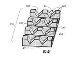
図4fは、次のステップの結果を示し、その間にマスキング層460、例えば二酸化シリコン(SiO2)又は窒化シリコン(SiN)系の又はそれからなる誘電層が、{111}方向の個別のファセット330’以外の全表面上に堆積される。このステップは、標準的なイオンビームスパッタリング(IBS)設備を使って実行され、堆積角度は、この場合、{111}方向のファセット330上で起こる堆積を防止するように調節できる。その結果、個別のファセット330’は、{111}方向を有し、相互に分離された個別のファセット330’のアレイ335を一緒に形成する。特に、マスキング層460は、例えば図4fからわかるように、{111}方向のファセットに対向するファセットを覆う。
FIG. 4f shows the result of the next step, in which the
図4gは、以下の材料Ga、In、及びAl(材料V-N)480のうちの少なくとも1つを用いて得られる窒化物の成長が、誘電マスキング層460により覆われていない個別の{111}ファセット330’からどのように開始されるかを示す。図4g及び4fに示されているように、このマスキング層460は、基板310と層480との間に配置される。矢印341は、前述のように、c面における成長の方向を示し、矢印472及び474は、本発明の構造中で成長が横方向にも延びてトレンチを埋める様子を示す。留意すべき点として、図4gは、明らかに成長の方向を示すことを目的としているにすぎず、現実を正確に表すものではない。実際には、エピタキシャル成長により、横方向の合体及び線上の合体、すなわち方向341、472、474の各々への成長が可能である。
FIG. 4g shows the individual {111] in which the growth of the nitride obtained using at least one of the following materials Ga, In, and Al (material VN) 480 is not covered by the dielectric masking layer 460. } Shows how to start from
成長は、主として方向341に起こる。
Growth occurs primarily in
その結果、成長は、{111}結晶方向を有する前記個別のファセット330’からのみ開始する。 As a result, growth begins only from said individual facets 330'with {111} crystal orientation.
より長い成長時間及び最適化された成長の条件において、結晶は溝から基板の表面の上方に向かう。これは、基本的に低いV-III比で得られてもよい。 Under longer growth times and optimized growth conditions, the crystals go from the grooves to above the surface of the substrate. This may be obtained at essentially a low V-III ratio.
最後に、図4hに示されるように、エピタキシャル材料の成長が継続し、最も高い位置の最終的な表面がV-N系の連続的な半極性層480を形成する間にすべての結晶の合体が得られる。
Finally, as shown in FIG. 4h, the growth of the epitaxial material continues and the coalescence of all crystals while the final surface at the highest position forms a continuous
図5a及び5bは、図4g及び4hに示されている構造の、{111}方向のファセットを通過する、{111}方向のファセットに垂直であり、且つ平行なトレンチに垂直な2つの断面図である。この断面の平面は、図4fにおいてPで示される。 5a and 5b are two cross-sectional views of the structure shown in FIGS. 4g and 4h, perpendicular to the facet in the {111} direction and perpendicular to the trench parallel to the facet in the {111} direction, passing through the facet in the {111} direction. Is. The plane of this cross section is shown by P in FIG. 4f.
これらの図面は、したがって{111}方向のファセット330’を示し、そこから核480の成長が開始する。ごく単純化された図4gと異なり、図5aは、核480の横方向の成長、すなわちトレンチ450内における上述の方向472及び474への成長を示す。成長の方向341、472、及び474は図5a及び5bにも示されている。したがって、横方向の成長は溝に沿って、エッチングされたトレンチの上方で起こる。この種のエピタキシは、ペンデオ・エピタキシと呼ばれてよい。
These drawings therefore show facets 330'in the {111} direction, from which
これらの{111}方向のファセット330’は、好ましくはマスキング層460で覆われているトレンチ541の底部の上方に位置付けられている。トレンチ450の底部451は、トレンチ450の窪んだ起伏部により形成される底部であり、この底部が1つ又は複数の層、例えばマスキング層460により覆われているか否かを問わない。この底部は、平坦であってもなくてもよい。
These {111} direction facets 330'are preferably located above the bottom of the trench 541 covered by the
図5aに示されているように、核480は合体前に「空洞の上方」に成長し、すなわち、これらはトレンチ450の底部451から離れて成長する。したがって、空洞の空間500、すなわち中実の材料のない部分が成長している核480と、マスキング層460により覆われる基板310との間に存在する。
As shown in FIG. 5a, the
その結果、その成長の少なくとも一部において、核480は、トレンチ450の底部451と接触することから生じる応力に曝されずに成長する。これにより、核480において、その成長の少なくとも一部において欠陥を減らすことが可能となる。したがって、最終的に得られた半極性層480中の欠陥が減少する。
As a result, at least in part of its growth, the
図5bに示されるように、非限定的であるが特に有利な実施形態によれば、核480の合体は、核480がトレンチ450の底部451と接触していないとき、又は核480がトレンチ450の底部451と完全には接触していないときに起こる。
As shown in FIG. 5b, according to a non-limiting but particularly advantageous embodiment, the coalescence of the
好ましくは、トレンチ450及び溝320の幅(方向472及び474に向かう)と深さ(基板310の厚さを通る)との寸法は、核の少なくともいくつかがトレンチ450の底部451と完全には接触することなく、核480の合体が可能にするように構成される。当然のことながら、マスキング層460の厚さも、成長する核480と接触しないような寸法とされる。
Preferably, the dimensions of the width (towards
ある有利な実施形態によれば、核480の少なくとも一部、好ましくは全部がトレンチ450の底部451から完全に離れている。したがって、これらの核は、トレンチ450の底部451と接触せず、また、トレンチの底部を覆うマスキング層460等の任意選択による層と接触しない。
According to one advantageous embodiment, at least a portion, preferably the
図5bは、したがって、各種の核の合体後、半極性層480と、任意選択によりマスキング層460により覆われているトレンチ450の底部との間に空間500が存在する実施形態を示す。
FIG. 5b therefore shows an embodiment in which a
好ましくは、空間500は、最終的な半極性層とトレンチ450の底部との間に存在する。
Preferably, the
これらの実施形態は、いくつかの非常に有利な技術的効果を提供する。 These embodiments provide some very advantageous technical benefits.
トレンチ450の上方、したがって「空洞の」空間500の上方で各種の核が合体することにより、合体中の応力をより良好に解放し、GaNの層における応力を減少させることができる。
The coalescence of various nuclei above the
その結果、横方向選択成長を経た領域における応力勾配のないエピタキシャル層が得られる。 The result is an epitaxial layer with no stress gradient in the region that has undergone lateral selective growth.
比較のために、「ELO」型(「エピタキシャル横方向選択成長」の略語)の構造は、上及び横方向のファセットの湾曲を誘発し、これは合体中の問題に反映される(転移及び生じ得る空洞の発生)。 For comparison, the "ELO" type (abbreviation for "epitaxial lateral selective growth") structure induces upward and lateral facet curvature, which is reflected in problems during coalescence (transitions and occurrences). Occurrence of cavities to obtain).
最終的に、本発明は、半極性層480の欠陥数を大幅に減らすことができる。
Finally, the present invention can significantly reduce the number of defects in the
さらに、トレンチの底部451の少なくとも一部分上にこの空間500が存在することにより、半極性層の剥離が、それと基板との間の界面がより脆弱になるために容易になる。したがって、本発明により、剥離中のGaNの層の破損のリスクを低減させることができる。
In addition, the presence of this
留意すべき点として、これらの技術的な効果及び利点は、半極性層480の一部がトレンチ450の底部451と接触していたとしても得られる。
It should be noted that these technical benefits and advantages are obtained even if part of the
本発明による製造方法の非限定的な例を以下に説明する。この方法の主要なステップは、図4a~4hに関してすでに説明した:
ステップ1:例えば、SiO2からなる保護層430のクリーンな基板310への堆積。堆積される層の厚さは約10nmで十分であるが、調節されてもよい。SiO2の代わりにSiN又はTiNも使用してよい。
ステップ2:整列して切り取られた第一のマスクを用いたリソグラフィと樹脂の成長。
ステップ3:樹脂が依然として上にある間に、露出した保護層(SiO2又はSiN又はTiN)が、例えば、酸素の存在中にトリフルオロメタンプラズマ(CHF3/O2プラズマ)中でエッチングされる。その他のエッチング溶液も使用されてよい。このステップは、その後のKOH又はTMAHでの異方性ウェットエッチングのための開口を作ることを目的としている。別の解決策によれば、緩衝酸化物エッチング溶液(BOE)を使ってマスクを除去してもよい。
ステップ4:樹脂がアセトン及び酸素のプラズマを使って除去される。
ステップ5:KOH又はTMAHでのエッチングを開始し、図4aに示されるような完全又は不完全なV溝320を形成する所望の{111}ファセット330を形成する。
ステップ6:溝の形成された基板を塩化水素(HCl)で洗浄し、KOHの結晶残留物を表面から除去する。
ステップ7:SiO2又SiN又はTiNの保護マスクを、緩衝エッチング溶液BOEを使って除去し、したがって、図4bに示されるように、全シリコンの切欠き部のある基板を得る。
ステップ8:整列した第二のマスクを用いたリソグラフィ。マスクは、任意選択により、第一のマスクと同じであってもよいが、異なる向きで使用される。リソグラフィは、その結果、V溝の深さに応じて適応される。例えば、5μmの深さのV溝には200mJの露光エネルギーが必要となり、最終的により長い現像時間が必要となる。例えば、深さ1μmのより浅い溝の場合、120mJのオーダのより低い露光エネルギーが必要となる。上述の数字はまた、使用される樹脂の種類及び結果的に得られる厚さにも依存してよい。
次に、樹脂が現像される(図4c)。
ステップ9:パターンを形成し、マスクとして使用される樹脂から開始して、シリコンの異方性エッチングを六フッ化硫黄(SF6)(又はその他のエッチング溶液)の誘導結合プラズマ(ICP)中で実施し、直線の側壁を有するトレンチ450を形成する(図4d)。
ステップ10:アセトン及び酸素のプラズマを使って樹脂を除去する。
ステップ11:SiO2又はSiN又はTiNの角堆積を{111}面以外の全表面に実行し、1方向cへのエピタキシャル層の成長を強制する。
ステップ12:マスキングされていない{111}面から開始して、以下の材料:ガリウム(Ga)、インジウム(In)、及びアルミニウム(Al)の少なくとも1つを用いて得られる窒化物の層をエピタキシャル成長させる。以下の材料:ガリウム(Ga)、インジウム(In)、及びアルミニウム(Al)の少なくとも1つを用いて得られる前記窒化物の性質に応じて、第一の層、典型的にはAlNがファセット330’上に最初に成長する。
A non-limiting example of the production method according to the present invention will be described below. The main steps of this method have already been described for FIGS. 4a-4h:
Step 1: For example, depositing a
Step 2: Lithography and resin growth using a first mask that is aligned and cut out.
Step 3: The exposed protective layer (SiO2 or SiN or TiN) is etched in a trifluoromethane plasma (CHF3 / O2 plasma), for example in the presence of oxygen, while the resin is still on top. Other etching solutions may also be used. This step is intended to create an opening for subsequent anisotropic wet etching with KOH or TMAH. According to another solution, the mask may be removed using a buffered oxide etching solution (BOE).
Step 4: The resin is removed using plasma of acetone and oxygen.
Step 5: Etching with KOH or TMAH is initiated to form the desired {111}
Step 6: The grooved substrate is washed with hydrogen chloride (HCl) to remove KOH crystal residues from the surface.
Step 7: The protection mask of SiO2 or SiN or TiN is removed using the buffered etching solution BOE, thus obtaining a substrate with a notch of all silicon, as shown in FIG. 4b.
Step 8: Lithography using an aligned second mask. The mask may be, optionally, the same as the first mask, but in a different orientation. Lithography is, as a result, adapted according to the depth of the V-groove. For example, a V-groove with a depth of 5 μm requires an exposure energy of 200 mJ, which ultimately requires a longer development time. For example, a shallower groove with a depth of 1 μm requires lower exposure energy on the order of 120 mJ. The numbers mentioned above may also depend on the type of resin used and the resulting thickness.
Next, the resin is developed (FIG. 4c).
Step 9: Anisotropic etching of silicon is performed in inductively coupled plasma (ICP) of sulfur hexafluoride (SF6) (or other etching solution), starting with the resin used as the mask to form the pattern. Then, a
Step 10: Remove the resin using plasma of acetone and oxygen.
Step 11: Square deposition of SiO2 or SiN or TiN is performed on all surfaces except the {111} plane to force the growth of the epitaxial layer in one direction c.
Step 12: Epitaxy growth of a layer of nitride obtained using at least one of the following materials: gallium (Ga), indium (In), and aluminum (Al), starting from the unmasked {111} plane: Let me. The following materials: Depending on the nature of the nitride obtained using at least one of gallium (Ga), indium (In), and aluminum (Al), the first layer, typically AlN, is faceted 330. 'Grow first on.
上記ステップ全体を通じて、マスクを形成する保護コーティングの代わりに、他の何れの種類のマスキング材料を用いてもよい。 Throughout the above steps, any other type of masking material may be used instead of the protective coating forming the mask.
実験では以下の成長速度が見られた:
- 半極性成長速度:1nm/s
- +c方向への成長速度:2.5nm/s、すなわち半極性方向への成長速度の約2.5倍。
The following growth rates were observed in the experiment:
-Semipolar growth rate: 1 nm / s
-Growth rate in the + c direction: 2.5 nm / s, that is, about 2.5 times the growth rate in the semi-polar direction.
本発明の実行に関するその他の詳細のいくつかを以下に示す。これらの詳細は、特に、上述の成長速度に関するGaN系のエピタキシャル層の成長に関する。
- 材料:V/IIIモル比は100~200である。この比は、できるだけ低く保持しなければならない。好ましい実施形態によれば、比V/IIIは440に略等しいが、440未満の数値でも同様の結果を得ることができ、2000までの数値に到達してもよい。これらの数値はまた、MOCVD(金属有機化学蒸着)リアクタの構成及び質量流量能力にも依存する。実験は、AIXTRON AG社製の直接制御(クローズカップルシャワーヘッドの省略CCS)方式のThomas Swanエピタキシリアクタを使って行った。
- 温度:有利には、温度は1000℃より高く保持される。これにより、結晶の品質を向上させることができる。それより低温ではファセットが波状になり得る。
- 圧力:圧力は、好ましくは、50~700mbarに保持される。しかしながら、圧力はリアクタの能力に依存する重要パラメータではないことがわかっている。
Some of the other details relating to the practice of the present invention are shown below. These details particularly relate to the growth of the GaN-based epitaxial layer with respect to the growth rate described above.
-Material: V / III molar ratio is 100-200. This ratio should be kept as low as possible. According to a preferred embodiment, the ratio V / III is approximately equal to 440, but similar results can be obtained with values less than 440 and may reach values up to 2000. These numbers also depend on the configuration and mass flow capacity of the MOCVD (Metalorganic Chemical Deposition) reactor. The experiment was carried out using a directly controlled (CCS abbreviated as closed couple shower head) Thomas Swan epitaxy reactor manufactured by AIXTRON AG.
-Temperature: Advantageously, the temperature is kept above 1000 ° C. Thereby, the quality of the crystal can be improved. At lower temperatures, the facets can wavy.
-Pressure: The pressure is preferably maintained at 50-700 mbar. However, it has been found that pressure is not an important parameter that depends on the capacity of the reactor.
これらの成長条件によれば、半極性層の成長方向を改善することができ、その結果、基板の表面上で結晶を得ることができる。 According to these growth conditions, the growth direction of the semi-polar layer can be improved, and as a result, crystals can be obtained on the surface of the substrate.
非限定的な実施形態によれば、本発明により得られるパターンは以下の寸法を有していてもよい:
- V溝320のピッチp1:このピッチp1はまた、第一のレベルのリソグラフィの期間として定義されてもよい。好ましくは、これは50nm≦p1≦15μmとなるような範囲内である。これは、大きい面積での処理を容易にしながら、効果的に合体させることができる。溝320のピッチp1は、溝の幅454に、2つの連続する溝を分離する距離を加算したものである。ピッチp1は、基板310の底部に平行な平面、すなわち説明されている図面内で水平の平面内で測定される。
- トレンチ450のピッチp2:このピッチp2はまた、第二のレベルのリソグラフィの期間として定義されてもよい。典型的に、p2は、p1より2.5倍小さくなるように選択される。例えば、p1が10μmと等しくなるように選択されると、p2は4μm±30%に近くなければならない。有利には、この比によって全方向への同時合体が確実に行われる。その結果、好ましい実施形態によれば、V溝320のピッチとトレンチ450のピッチとは相応に調節される。トレンチ450のピッチp2は、トレンチの幅に、2つの連続するトレンチ450を分離する距離を加算したものである。ピッチp2は、基板310の底部に平行な、すなわち、説明されている図面内の水平な平面内で測定される。
- 以下の材料:ガリウム(Ga)、インジウム(In)、及びアルミニウム(Al)のうちの少なくとも1つを用いて得られる窒化物のエピタキシャル成長がそこから開始するファセットの寸法:このファセットの寸法は、50nmからピッチ及び開口に依存する完全なV溝の数値までの範囲である。
According to a non-limiting embodiment, the pattern obtained by the present invention may have the following dimensions:
-Pitch p1 of V-
-Pitch p2 of trench 450: This pitch p2 may also be defined as a period of second level lithography. Typically, p2 is selected to be 2.5 times smaller than p1. For example, if p1 is chosen to be equal to 10 μm, p2 should be close to 4 μm ± 30%. Advantageously, this ratio ensures simultaneous coalescence in all directions. As a result, according to the preferred embodiment, the pitch of the V-
-The following materials: Dimensions of the facet from which the epitaxial growth of the nitride obtained using at least one of gallium (Ga), indium (In), and aluminum (Al) begins: The dimensions of this facet are: It ranges from 50 nm to full V-groove values that depend on pitch and aperture.
基板とV-N系材料の成長層との間の接触を減らすことにより、発生する欠陥の数が減る。転移の連鎖の空間分布の点で、この基板構成により、基板/V-N材料の界面の接触により発生する初期欠陥の数を減らすことができる。 By reducing the contact between the substrate and the growth layer of the VN-based material, the number of defects generated is reduced. In terms of the spatial distribution of the transition chain, this substrate configuration can reduce the number of initial defects generated by the interface contact between the substrate / VN material.
さらに、本発明の方法により、合体前により多くの結晶領域を形成することができ、これは、基底面に沿った転移の曲がりがより大きくなり、その結果、表面に広がる転移がより少なくなることを意味し、これはP.Vennegues et al.“Reduction mechanisms for defect densities in the V-N material using one- or two-step epitaxial lateral overgrowth methods”,JOURNAL OF APPLIED PHYSICS.AMERICAN INSTITUTE OF PHYSICS,NEW YORK,US,Vol.87,no.9,1 May 2000(2000-05-01),Pages 4175-4181の著作物で説明されている。 In addition, the method of the invention allows the formation of more crystalline regions prior to coalescence, which results in greater bending of the transition along the basal plane and, as a result, less transition spreading to the surface. Means, this is P. Vennegues et al. "Reduction mechanisms for defects in the V-N material using one-or two-step applied physical lateral epitaxy methods", JOURNAL OFPL AMERICAN INSTITUTE OF PHYSICS, NEW YORK, US, Vol. 87, no. It is described in the work of 9,1 May 2000 (2000-05-01), Pages 4175-4181.
基底面積層欠陥(BSF)の分布に関して、BSFは成長方向-cから開始することがわかっているため、本発明のピラー構造の製作により、-c面における拡張がさらに減少し、これがBSFの低減化につながる。 With respect to the distribution of basal area layer defects (BSF), it is known that BSF starts from the growth direction -c, so the fabrication of the pillar structure of the present invention further reduces the expansion in the -c plane, which reduces BSF. It leads to the change.
上述の説明から、本発明により、以下の材料:ガリウム(Ga)、インジウム(In)、及びアルミニウム(Al)のうちの少なくとも1つを用いて得られた窒化物のエピタキシャル層をシリコン基板上において成長させる際の結晶構造の欠陥を削減できることが明らかである。 From the above description, according to the present invention, an epitaxial layer of a nitride obtained using at least one of the following materials: gallium (Ga), indium (In), and aluminum (Al) is placed on a silicon substrate. It is clear that defects in the crystal structure during growth can be reduced.
したがって、本発明により、より高効率の緑色LEDを得ることが可能となる。 Therefore, according to the present invention, it is possible to obtain a green LED with higher efficiency.
本発明は、上述の実施形態に限定されず、特許請求の範囲により包含される実施形態のすべてに及ぶ。 The present invention is not limited to the above-described embodiments, but extends to all embodiments included in the claims.
Claims (30)
- 前記結晶基板(310)の前記上面上において、主として第一の方向に延びる複数の平行な溝(320、410、420)を得るステップであって、各溝(320、410、420)は、連続的であり、各溝(320、410、420)は、少なくとも2つの対向する傾斜ファセット(330、331)を含み、前記2つの対向するファセット(330、331)のうちの少なくとも1つ(330)は、{111}結晶方向を有する、ステップと、
- {111}結晶方向を有する前記ファセット(330)に対向する前記ファセット(331)がマスキングされ、且つ{111}結晶方向を有する前記ファセット(330)がマスキングされないように、前記結晶基板(310)の前記上面をマスキングするステップと、
- 前記半極性層(480)をエピタキシャル成長させるステップと
を含む、方法において、前記複数の平行な溝(320、410、420)を得る前記ステップの後、且つ前記半極性層(480)をエピタキシャル成長させる前記ステップの前に実行される以下のステップ:
- 前記溝(320、410、420)の前記第一の方向に関して回転させた後の第二の方向に延び、したがって前記連続する溝(320、410、420)を中断して、それぞれ{111}結晶方向を有する個別のファセット(330’)のアレイ(335)を形成する複数の平行なトレンチ(450)をエッチングするステップであって、前記トレンチ(450)及び前記溝(320、410、420)は、それぞれ底部(451)を有し、前記トレンチ(450)の前記底部(451)は、前記溝(320、410、420)の前記底部(411、421)と同じ深さ又はそれより下方に配置される、ステップ
も含むことと、
エピタキシャル成長させる前記ステップ中、前記材料は、{111}結晶方向を有し、且つ前記アレイ(335)を形成する前記個別のファセット(330’)から開始してのみ成長することとを特徴とする方法。 A crystal substrate (310) having at least one semi-polar layer (480) of at least one material containing nitride (N) and at least one of gallium (Ga), indium (In), and aluminum (Al). A method of obtaining on the top surface of the following steps:
-A step of obtaining a plurality of parallel grooves (320, 410, 420) extending mainly in the first direction on the upper surface of the crystal substrate (310), wherein each groove (320, 410, 420) is formed. Continuous, each groove (320, 410, 420) comprises at least two opposing inclined facets (330, 331) and at least one of the two opposing facets (330, 331) (330). ) Shall have a {111} crystal direction, a step and
-The crystal substrate (310) so that the facet (331) facing the facet (330) having a {111} crystal direction is masked and the facet (330) having a {111} crystal direction is not masked. And the step of masking the upper surface of
-In a method comprising epitaxially growing the semi-polar layer (480), after the step of obtaining the plurality of parallel grooves (320, 410, 420) and epitaxially growing the semi-polar layer (480). The following steps performed prior to the step:
-The groove (320, 410, 420) extends in a second direction after being rotated with respect to the first direction, thus interrupting the continuous groove (320, 410, 420), respectively {111}. A step of etching a plurality of parallel trenches (450) forming an array (335) of individual facets (330') with crystal orientation, said trench (450) and said groove (320, 410, 420). Each has a bottom (451), and the bottom (451) of the trench (450) is at or below the same depth as the bottom (411, 421) of the groove (320, 410, 420). Being placed, including steps,
During the epitaxial growth process, the material has a {111} crystal direction and grows only starting from the individual facets (330') forming the array (335). ..
- {111}結晶方向を有し、且つ前記アレイ(335)を形成する前記個別のファセット(330’)から開始する、窒化アルミニウム(AlN)系材料の第一のエピタキシャル成長と、
- エピタキシャル成長後の前記窒化アルミニウム(AlN)系材料から開始する、窒化ガリウム(GaN)系材料(480)の少なくとも1つの第二のエピタキシャル成長と
を含む、請求項1~24の何れか一項に記載の方法。 The step of epitaxially growing is
-With the first epitaxial growth of the aluminum nitride (AlN) -based material, starting from the individual facets (330') having a {111} crystal orientation and forming the array (335).
-The invention of any one of claims 1-24, comprising at least one second epitaxial growth of the gallium nitride (GaN) -based material (480) starting from the aluminum nitride (AlN) -based material after epitaxial growth. the method of.
- 前記基板は、第一の方向に延びる複数の平行な溝(を含み、各溝は、それぞれ前記第一の方向に延びる連続的な帯を形成する少なくとも2つの対向する傾斜ファセットを含み、前記2つの対向するファセットのうちの少なくとも1つは、{111}結晶方向を有する、マイクロエレクトロニックデバイスにおいて、
前記基板は、前記第一の方向とは平行ではない第二の方向に延びる複数の平行なトレンチも含み、
前記複数の平行な溝と前記複数の平行なトレンチとの組合せは、{111}結晶方向を有する個別のファセットのアレイを画定し、
前記トレンチ及び前記溝は、それぞれ底部を有し、前記トレンチの前記底部は、前記溝の前記底部より下方に配置され、
前記材料は、結晶方向を有する前記個別のファセットと直接接触し、
前記デバイスは、前記基板と前記材料との間に配置され、且つ結晶方向を有する前記個別のファセット以外の、前記基板の前記上面の全体を覆うマスキング層も含むことを特徴とするマイクロエレクトロニックデバイス。 A semi-polar layer of a crystal substrate and at least one material on the upper surface of the crystal substrate, comprising a nitride (N) and at least one of gallium (Ga), indium (In), and aluminum (Al). Is a microelectronic device that includes
-The substrate comprises a plurality of parallel grooves extending in the first direction, each groove containing at least two opposing inclined facets forming a continuous band extending in the first direction. At least one of the two opposing facets has a {111} crystal orientation in a microelectronic device.
The substrate also includes a plurality of parallel trenches extending in a second direction that is not parallel to the first direction.
The combination of the plurality of parallel grooves and the plurality of parallel trenches defines an array of individual facets having a {111} crystal orientation.
The trench and the groove each have a bottom, and the bottom of the trench is arranged below the bottom of the groove.
The material is in direct contact with the individual facets having a crystallographic orientation.
The device is a microelectronic device that is disposed between the substrate and the material and also includes a masking layer that covers the entire upper surface of the substrate other than the individual facets having a crystallographic direction.
Applications Claiming Priority (5)
| Application Number | Priority Date | Filing Date | Title |
|---|---|---|---|
| FR1555582A FR3037711A1 (en) | 2015-06-18 | 2015-06-18 | PROCESS FOR OBTAINING ON A CRYSTALLINE SUBSTRATE A SEMI-POLAR NITRIDE LAYER OBTAINED WITH AT LEAST ONE OF THE FOLLOWING MATERIALS: GALLIUM (GA), INDIUM (IN) AND ALUMINUM (AL) |
| FR1555582 | 2015-06-18 | ||
| FR1561618A FR3037713B1 (en) | 2015-06-18 | 2015-11-30 | PROCESS FOR OBTAINING ON A CRYSTALLINE SUBSTRATE A SEMI-POLAR NITRIDE LAYER OBTAINED WITH AT LEAST ONE OF THE FOLLOWING MATERIALS: GALLIUM (GA), INDIUM (IN) AND ALUMINUM (AL) |
| FR1561618 | 2015-11-30 | ||
| PCT/EP2016/063824 WO2016202899A1 (en) | 2015-06-18 | 2016-06-16 | Method making it possible to obtain on a crystalline substrate a semi-polar layer of nitride obtained with at least one of the following materials: gallium (ga), indium (in) and aluminium (al) |
Publications (2)
| Publication Number | Publication Date |
|---|---|
| JP2018520977A JP2018520977A (en) | 2018-08-02 |
| JP7000163B2 true JP7000163B2 (en) | 2022-01-19 |
Family
ID=54356447
Family Applications (1)
| Application Number | Title | Priority Date | Filing Date |
|---|---|---|---|
| JP2017565193A Active JP7000163B2 (en) | 2015-06-18 | 2016-06-16 | A method that makes it possible to obtain a semi-polar layer of a nitride obtained by using at least one of the following materials: gallium (Ga), indium (In), and aluminum (Al) on a crystalline substrate. |
Country Status (5)
| Country | Link |
|---|---|
| US (1) | US11139167B2 (en) |
| EP (1) | EP3311394B1 (en) |
| JP (1) | JP7000163B2 (en) |
| FR (2) | FR3037711A1 (en) |
| WO (1) | WO2016202899A1 (en) |
Families Citing this family (6)
| Publication number | Priority date | Publication date | Assignee | Title |
|---|---|---|---|---|
| FR3048002B1 (en) * | 2016-02-22 | 2021-07-02 | Commissariat Energie Atomique | PROCESS FOR OBTAINING A SEMI-POLAR LAYER OF NITRIDE ON A CRYSTALLINE SUBSTRATE |
| TWI728364B (en) * | 2019-05-21 | 2021-05-21 | 國立陽明交通大學 | SEMICONDUCTOR STRUCTURE OF GaN EPITAXY IN HETEROINTEGRATION WITH Si SUBSTRATE AND METHOD OF MANUFACTURING THE SAME |
| US11120990B2 (en) * | 2019-07-19 | 2021-09-14 | Alliance For Sustainable Energy, Llc | Methods for depositing III-V compositions on silicon |
| US11515408B2 (en) * | 2020-03-02 | 2022-11-29 | Taiwan Semiconductor Manufacturing Company, Ltd. | Rough buffer layer for group III-V devices on silicon |
| FR3118306B1 (en) * | 2020-12-22 | 2023-05-05 | Commissariat Energie Atomique | Method for producing an optoelectronic device comprising nitride-based LEDs |
| CN114447159A (en) * | 2022-02-10 | 2022-05-06 | 武汉新芯集成电路制造有限公司 | Semiconductor device and method of forming the same |
Citations (1)
| Publication number | Priority date | Publication date | Assignee | Title |
|---|---|---|---|---|
| US20120276722A1 (en) | 2011-04-27 | 2012-11-01 | Jen-Inn Chyi | Method for growing semipolar nitride |
Family Cites Families (6)
| Publication number | Priority date | Publication date | Assignee | Title |
|---|---|---|---|---|
| JP5353113B2 (en) * | 2008-01-29 | 2013-11-27 | 豊田合成株式会社 | Method for producing group III nitride compound semiconductor |
| US8664747B2 (en) * | 2008-04-28 | 2014-03-04 | Toshiba Techno Center Inc. | Trenched substrate for crystal growth and wafer bonding |
| GB2460898B (en) * | 2008-06-19 | 2012-10-10 | Wang Nang Wang | Production of semiconductor material and devices using oblique angle etched templates |
| TW201108328A (en) * | 2009-08-21 | 2011-03-01 | Univ Nat Central | Method for fabricating a semi-polar nitride semiconductor |
| DE102010011895B4 (en) * | 2010-03-18 | 2013-07-25 | Freiberger Compound Materials Gmbh | Process for the preparation of a group III nitride semipolar crystal, substrate, free-standing semipolar substrate and use of the substrates |
| JP5573632B2 (en) * | 2010-11-25 | 2014-08-20 | 豊田合成株式会社 | Group III nitride semiconductor light emitting device |
-
2015
- 2015-06-18 FR FR1555582A patent/FR3037711A1/en active Pending
- 2015-11-30 FR FR1561618A patent/FR3037713B1/en not_active Expired - Fee Related
-
2016
- 2016-06-16 WO PCT/EP2016/063824 patent/WO2016202899A1/en active Application Filing
- 2016-06-16 JP JP2017565193A patent/JP7000163B2/en active Active
- 2016-06-16 US US15/736,270 patent/US11139167B2/en active Active
- 2016-06-16 EP EP16731090.3A patent/EP3311394B1/en active Active
Patent Citations (1)
| Publication number | Priority date | Publication date | Assignee | Title |
|---|---|---|---|---|
| US20120276722A1 (en) | 2011-04-27 | 2012-11-01 | Jen-Inn Chyi | Method for growing semipolar nitride |
Also Published As
| Publication number | Publication date |
|---|---|
| US20180182622A1 (en) | 2018-06-28 |
| FR3037713A1 (en) | 2016-12-23 |
| EP3311394B1 (en) | 2022-01-19 |
| JP2018520977A (en) | 2018-08-02 |
| FR3037713B1 (en) | 2017-06-09 |
| EP3311394A1 (en) | 2018-04-25 |
| US11139167B2 (en) | 2021-10-05 |
| WO2016202899A1 (en) | 2016-12-22 |
| FR3037711A1 (en) | 2016-12-23 |
Similar Documents
| Publication | Publication Date | Title |
|---|---|---|
| JP7000163B2 (en) | A method that makes it possible to obtain a semi-polar layer of a nitride obtained by using at least one of the following materials: gallium (Ga), indium (In), and aluminum (Al) on a crystalline substrate. | |
| US9034739B2 (en) | Semiconductor devices and fabrication methods | |
| US8188573B2 (en) | Nitride semiconductor structure | |
| JP2010512301A (en) | Crystal growth of (Al, In, Ga, B) N M-plane and semipolar plane on various substrates | |
| US9355840B2 (en) | High quality devices growth on pixelated patterned templates | |
| TW201405635A (en) | Selective sidewall growth of semiconductor material | |
| US9660135B2 (en) | Enhanced performance active pixel array and epitaxial growth method for achieving the same | |
| JP2006036561A (en) | Method for growing semiconductor crystal, optical semiconductor element, and substrate for crystal growth | |
| JP2007184503A (en) | Semiconductor member and manufacturing method thereof | |
| EP3075002A1 (en) | Semiconductor devices and fabrication methods | |
| JP2010147164A (en) | Method of manufacturing semiconductor element | |
| JP2007184504A (en) | Semiconductor member, and method of manufacturing same | |
| JP5174052B2 (en) | Method for producing epitaxial structure with low defect density | |
| TWI451480B (en) | Method for fabricating group iii-nitride semiconductor | |
| US20100184279A1 (en) | Method of Making an Epitaxial Structure Having Low Defect Density | |
| US9391235B2 (en) | Patterned substrate for epitaxially growing semiconductor material, and method for patterning a substrate | |
| JP2009184860A (en) | Substrate and epitaxial wafer | |
| US20110114983A1 (en) | Photoelectric device having group iii nitride semiconductor | |
| JP2013249231A (en) | Method for manufacturing semiconductor substrate of periodic table group 13 metal nitride | |
| JP2007184432A (en) | Method of manufacturing semiconductor stack structure, and semiconductor element formed thereon |
Legal Events
| Date | Code | Title | Description |
|---|---|---|---|
| A621 | Written request for application examination |
Free format text: JAPANESE INTERMEDIATE CODE: A621 Effective date: 20190605 |
|
| A977 | Report on retrieval |
Free format text: JAPANESE INTERMEDIATE CODE: A971007 Effective date: 20200626 |
|
| A131 | Notification of reasons for refusal |
Free format text: JAPANESE INTERMEDIATE CODE: A131 Effective date: 20200707 |
|
| A601 | Written request for extension of time |
Free format text: JAPANESE INTERMEDIATE CODE: A601 Effective date: 20201001 |
|
| A521 | Request for written amendment filed |
Free format text: JAPANESE INTERMEDIATE CODE: A523 Effective date: 20201225 |
|
| A131 | Notification of reasons for refusal |
Free format text: JAPANESE INTERMEDIATE CODE: A131 Effective date: 20210601 |
|
| A521 | Request for written amendment filed |
Free format text: JAPANESE INTERMEDIATE CODE: A523 Effective date: 20210827 |
|
| TRDD | Decision of grant or rejection written | ||
| A01 | Written decision to grant a patent or to grant a registration (utility model) |
Free format text: JAPANESE INTERMEDIATE CODE: A01 Effective date: 20211124 |
|
| A61 | First payment of annual fees (during grant procedure) |
Free format text: JAPANESE INTERMEDIATE CODE: A61 Effective date: 20211223 |
|
| R150 | Certificate of patent or registration of utility model |
Ref document number: 7000163 Country of ref document: JP Free format text: JAPANESE INTERMEDIATE CODE: R150 |
|
| S111 | Request for change of ownership or part of ownership |
Free format text: JAPANESE INTERMEDIATE CODE: R313117 |
|
| R350 | Written notification of registration of transfer |
Free format text: JAPANESE INTERMEDIATE CODE: R350 |