JP6996467B2 - Elastic wave device - Google Patents
Elastic wave device Download PDFInfo
- Publication number
- JP6996467B2 JP6996467B2 JP2018187860A JP2018187860A JP6996467B2 JP 6996467 B2 JP6996467 B2 JP 6996467B2 JP 2018187860 A JP2018187860 A JP 2018187860A JP 2018187860 A JP2018187860 A JP 2018187860A JP 6996467 B2 JP6996467 B2 JP 6996467B2
- Authority
- JP
- Japan
- Prior art keywords
- substrate
- main surface
- elastic wave
- wave device
- protective layer
- Prior art date
- Legal status (The legal status is an assumption and is not a legal conclusion. Google has not performed a legal analysis and makes no representation as to the accuracy of the status listed.)
- Active
Links
- 239000000758 substrate Substances 0.000 claims description 147
- 239000010410 layer Substances 0.000 claims description 119
- 239000011241 protective layer Substances 0.000 claims description 103
- 125000006850 spacer group Chemical group 0.000 claims description 64
- 230000000149 penetrating effect Effects 0.000 claims description 21
- 239000010408 film Substances 0.000 description 73
- 239000011347 resin Substances 0.000 description 44
- 229920005989 resin Polymers 0.000 description 44
- 238000012986 modification Methods 0.000 description 15
- 230000004048 modification Effects 0.000 description 15
- 238000004519 manufacturing process Methods 0.000 description 13
- 239000000463 material Substances 0.000 description 11
- PXHVJJICTQNCMI-UHFFFAOYSA-N Nickel Chemical compound [Ni] PXHVJJICTQNCMI-UHFFFAOYSA-N 0.000 description 9
- 229910052751 metal Inorganic materials 0.000 description 8
- 239000002184 metal Substances 0.000 description 8
- 230000001681 protective effect Effects 0.000 description 7
- 229910045601 alloy Inorganic materials 0.000 description 6
- 239000000956 alloy Substances 0.000 description 6
- 150000002739 metals Chemical class 0.000 description 6
- 230000001902 propagating effect Effects 0.000 description 6
- 239000010949 copper Substances 0.000 description 5
- BASFCYQUMIYNBI-UHFFFAOYSA-N platinum Chemical compound [Pt] BASFCYQUMIYNBI-UHFFFAOYSA-N 0.000 description 5
- RYGMFSIKBFXOCR-UHFFFAOYSA-N Copper Chemical compound [Cu] RYGMFSIKBFXOCR-UHFFFAOYSA-N 0.000 description 4
- 229910052802 copper Inorganic materials 0.000 description 4
- 230000000694 effects Effects 0.000 description 4
- 239000010931 gold Substances 0.000 description 4
- 238000010438 heat treatment Methods 0.000 description 4
- 238000010030 laminating Methods 0.000 description 4
- 239000012528 membrane Substances 0.000 description 4
- 239000007769 metal material Substances 0.000 description 4
- 229910052759 nickel Inorganic materials 0.000 description 4
- 230000002093 peripheral effect Effects 0.000 description 4
- 238000010897 surface acoustic wave method Methods 0.000 description 4
- 239000011651 chromium Substances 0.000 description 3
- 238000010292 electrical insulation Methods 0.000 description 3
- 239000003822 epoxy resin Substances 0.000 description 3
- PCHJSUWPFVWCPO-UHFFFAOYSA-N gold Chemical compound [Au] PCHJSUWPFVWCPO-UHFFFAOYSA-N 0.000 description 3
- 229910052737 gold Inorganic materials 0.000 description 3
- 238000000034 method Methods 0.000 description 3
- 229920000647 polyepoxide Polymers 0.000 description 3
- 229920001721 polyimide Polymers 0.000 description 3
- 239000009719 polyimide resin Substances 0.000 description 3
- 229920003002 synthetic resin Polymers 0.000 description 3
- 239000000057 synthetic resin Substances 0.000 description 3
- 239000010936 titanium Substances 0.000 description 3
- VYZAMTAEIAYCRO-UHFFFAOYSA-N Chromium Chemical compound [Cr] VYZAMTAEIAYCRO-UHFFFAOYSA-N 0.000 description 2
- ZOKXTWBITQBERF-UHFFFAOYSA-N Molybdenum Chemical compound [Mo] ZOKXTWBITQBERF-UHFFFAOYSA-N 0.000 description 2
- BQCADISMDOOEFD-UHFFFAOYSA-N Silver Chemical compound [Ag] BQCADISMDOOEFD-UHFFFAOYSA-N 0.000 description 2
- RTAQQCXQSZGOHL-UHFFFAOYSA-N Titanium Chemical compound [Ti] RTAQQCXQSZGOHL-UHFFFAOYSA-N 0.000 description 2
- 238000002679 ablation Methods 0.000 description 2
- 229910052782 aluminium Inorganic materials 0.000 description 2
- XAGFODPZIPBFFR-UHFFFAOYSA-N aluminium Chemical compound [Al] XAGFODPZIPBFFR-UHFFFAOYSA-N 0.000 description 2
- 229910052804 chromium Inorganic materials 0.000 description 2
- 230000006866 deterioration Effects 0.000 description 2
- 238000010586 diagram Methods 0.000 description 2
- 239000012777 electrically insulating material Substances 0.000 description 2
- 238000009713 electroplating Methods 0.000 description 2
- -1 for example Substances 0.000 description 2
- 239000011261 inert gas Substances 0.000 description 2
- 229910052750 molybdenum Inorganic materials 0.000 description 2
- 239000011733 molybdenum Substances 0.000 description 2
- 229910052697 platinum Inorganic materials 0.000 description 2
- 238000007789 sealing Methods 0.000 description 2
- 229910052709 silver Inorganic materials 0.000 description 2
- 239000004332 silver Substances 0.000 description 2
- 229910000679 solder Inorganic materials 0.000 description 2
- 229910052719 titanium Inorganic materials 0.000 description 2
- WFKWXMTUELFFGS-UHFFFAOYSA-N tungsten Chemical compound [W] WFKWXMTUELFFGS-UHFFFAOYSA-N 0.000 description 2
- 229910052721 tungsten Inorganic materials 0.000 description 2
- 239000010937 tungsten Substances 0.000 description 2
- WSMQKESQZFQMFW-UHFFFAOYSA-N 5-methyl-pyrazole-3-carboxylic acid Chemical compound CC1=CC(C(O)=O)=NN1 WSMQKESQZFQMFW-UHFFFAOYSA-N 0.000 description 1
- 229910013641 LiNbO 3 Inorganic materials 0.000 description 1
- 239000003990 capacitor Substances 0.000 description 1
- 238000005516 engineering process Methods 0.000 description 1
- 239000007789 gas Substances 0.000 description 1
- 230000001678 irradiating effect Effects 0.000 description 1
- GQYHUHYESMUTHG-UHFFFAOYSA-N lithium niobate Chemical compound [Li+].[O-][Nb](=O)=O GQYHUHYESMUTHG-UHFFFAOYSA-N 0.000 description 1
- 238000000206 photolithography Methods 0.000 description 1
- 239000010453 quartz Substances 0.000 description 1
- VYPSYNLAJGMNEJ-UHFFFAOYSA-N silicon dioxide Inorganic materials O=[Si]=O VYPSYNLAJGMNEJ-UHFFFAOYSA-N 0.000 description 1
- 229920001187 thermosetting polymer Polymers 0.000 description 1
- 239000010409 thin film Substances 0.000 description 1
Images


Classifications
-
- H—ELECTRICITY
- H03—ELECTRONIC CIRCUITRY
- H03H—IMPEDANCE NETWORKS, e.g. RESONANT CIRCUITS; RESONATORS
- H03H9/00—Networks comprising electromechanical or electro-acoustic elements; Electromechanical resonators
- H03H9/02—Details
- H03H9/02535—Details of surface acoustic wave devices
- H03H9/02543—Characteristics of substrate, e.g. cutting angles
- H03H9/02574—Characteristics of substrate, e.g. cutting angles of combined substrates, multilayered substrates, piezoelectrical layers on not-piezoelectrical substrate
-
- H—ELECTRICITY
- H03—ELECTRONIC CIRCUITRY
- H03H—IMPEDANCE NETWORKS, e.g. RESONANT CIRCUITS; RESONATORS
- H03H9/00—Networks comprising electromechanical or electro-acoustic elements; Electromechanical resonators
- H03H9/02—Details
- H03H9/02535—Details of surface acoustic wave devices
- H03H9/02614—Treatment of substrates, e.g. curved, spherical, cylindrical substrates ensuring closed round-about circuits for the acoustical waves
-
- H—ELECTRICITY
- H03—ELECTRONIC CIRCUITRY
- H03H—IMPEDANCE NETWORKS, e.g. RESONANT CIRCUITS; RESONATORS
- H03H9/00—Networks comprising electromechanical or electro-acoustic elements; Electromechanical resonators
- H03H9/02—Details
- H03H9/02535—Details of surface acoustic wave devices
- H03H9/02818—Means for compensation or elimination of undesirable effects
- H03H9/02897—Means for compensation or elimination of undesirable effects of strain or mechanical damage, e.g. strain due to bending influence
Landscapes
- Physics & Mathematics (AREA)
- Acoustics & Sound (AREA)
- Surface Acoustic Wave Elements And Circuit Networks Thereof (AREA)
Description
本発明は、一般に弾性波装置に関し、特に、共振子又はフィルタに用いられる弾性波装置に関する。 The present invention relates to elastic wave devices in general, and more particularly to elastic wave devices used in resonators or filters.
従来、共振子又はフィルタに用いられる弾性波装置が知られている(例えば特許文献1参照)。 Conventionally, an elastic wave device used for a resonator or a filter is known (see, for example, Patent Document 1).
特許文献1に記載された弾性波装置は、圧電基板と、IDT電極を含む振動部と、支持層(スペーサ層)と、カバー層(カバー部材)と、保護層とを備える。特許文献1に記載された弾性波装置では、圧電基板の上にIDT電極が形成されている。また、特許文献1に記載された弾性波装置では、振動部の周囲において枠状に支持層が形成されており、支持層の上にカバー層が配置され、カバー層の上に保護層が形成されている。
The elastic wave device described in
ところで、特許文献1に記載された従来の弾性波装置を実装基板に実装させる際に、弾性波装置に対して実装基板が傾いている場合がある。このような場合、特許文献1に記載された従来の弾性波装置では、弾性波装置における保護層の角部が実装基板に衝突することがあった。つまり、実装基板への弾性波装置の角あたりが発生することがあった。このため、保護層又は実装基板にクラックが発生する可能性があるという問題があった。
By the way, when the conventional elastic wave device described in
本発明は上記の点に鑑みてなされた発明であり、本発明の目的は、クラックを発生しにくくすることができる弾性波装置を提供することにある。 The present invention has been made in view of the above points, and an object of the present invention is to provide an elastic wave device capable of making cracks less likely to occur.
本発明の一態様に係る弾性波装置は、基板と、IDT電極と、スペーサ層と、カバー部材と、保護層と、外部接続電極とを備える。前記基板は、少なくとも一部に圧電性を有する。前記IDT電極は、前記基板上に設けられている。前記スペーサ層は、前記基板上に設けられており、かつ、前記IDT電極を囲んでいる。前記カバー部材は、前記スペーサ層上に設けられており、前記IDT電極から離れている。前記カバー部材は、前記スペーサ層側の第1主面と、前記第1主面と対向する第2主面とを有する。前記保護層は、前記カバー部材上に設けられており、前記第2主面と接する第3主面と、前記第3主面と対向する第4主面と、前記第4主面に連なる側面とを有する。前記外部接続電極は、前記IDT電極に電気的に接続されている。前記外部接続電極は、前記スペーサ層と前記カバー部材と前記保護層とを貫通する貫通ビアを含む。前記保護層における前記側面のうちの少なくとも一部において、前記側面と前記第4主面との交線は、前記基板の厚さ方向からの平面視において、前記第4主面と前記基板との間であって前記基板と平行な任意の仮想平面と前記側面との交線よりも内側に位置する。 The elastic wave device according to one aspect of the present invention includes a substrate, an IDT electrode, a spacer layer, a cover member, a protective layer, and an external connection electrode . The substrate has piezoelectricity at least in part. The IDT electrode is provided on the substrate. The spacer layer is provided on the substrate and surrounds the IDT electrode. The cover member is provided on the spacer layer and is separated from the IDT electrode. The cover member has a first main surface on the spacer layer side and a second main surface facing the first main surface. The protective layer is provided on the cover member, and has a third main surface in contact with the second main surface, a fourth main surface facing the third main surface, and a side surface connected to the fourth main surface. And have. The external connection electrode is electrically connected to the IDT electrode. The external connection electrode includes a penetrating via that penetrates the spacer layer, the cover member, and the protective layer. In at least a part of the side surface of the protective layer, the line of intersection between the side surface and the fourth main surface is a plan view of the substrate from the thickness direction of the fourth main surface and the substrate. It is located inside the line of intersection between any virtual plane parallel to the substrate and the side surface.
本発明の上記態様に係る弾性波装置によれば、クラックを発生しにくくすることができる。 According to the elastic wave device according to the above aspect of the present invention, it is possible to make it difficult for cracks to occur.
以下、実施形態1,2に係る弾性波装置について、図面を参照して説明する。 Hereinafter, the elastic wave apparatus according to the first and second embodiments will be described with reference to the drawings.
下記の実施形態等において説明する図1~図3、図4A~図4F、図5A~図5E、及び図6は、模式的な図であり、図中の各構成要素の大きさや厚さそれぞれの比が、必ずしも実際の寸法比を反映しているとは限らない。また、図1は、図2のX1-X1線断面図である。 1 to 3, FIGS. 4A to 4F, FIGS. 5A to 5E, and FIG. 6 described in the following embodiments are schematic views, and the sizes and thicknesses of the respective components in the drawings are respectively. The ratio of does not always reflect the actual dimensional ratio. Further, FIG. 1 is a cross-sectional view taken along the line X1-X1 of FIG.
(実施形態1)
(1)弾性波装置の全体構成
まず、実施形態1に係る弾性波装置の全体構成について、図面を参照して説明する。
(Embodiment 1)
(1) Overall Configuration of Elastic Wave Device First, the overall configuration of the elastic wave device according to the first embodiment will be described with reference to the drawings.
実施形態1に係る弾性波装置1は、図1に示すように、基板11と、IDT(Interdigital Transducer)電極12と、スペーサ層13と、カバー部材14と、保護層15と、複数(図示例では2つ)の配線層16と、複数(図示例では2つ)の外部接続電極17とを備える。実施形態1に係る弾性波装置1は、WLP(Wafer Level Package:ウェハレベルパッケージ)型の弾性波装置であり、例えばSAW(Surface Acoustic Wave:弾性表面波)フィルタとして用いられる。ここでは、WLP型の弾性波装置1とは、ウェハレベルで、基板11にIDT電極12とスペーサ層13とカバー部材14と保護層15と配線層16と外部接続電極17とを設けるための工程を行い、最後に、ウェハを切断して得られるタイプの弾性波装置である。
As shown in FIG. 1, the
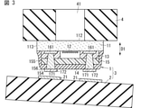
弾性波装置1は、図3に示すように、実装基板2に実装される。弾性波装置1と実装基板2とで電子部品モジュール3を構成する。
As shown in FIG. 3, the
(2)弾性波装置の各構成要素
次に、実施形態1に係る弾性波装置1の各構成要素について、図面を参照して説明する。
(2) Each Component of the Elastic Wave Device Next, each component of the
(2.1)基板
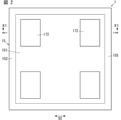
基板11は、図1に示すように、IDT電極12を支持している。基板11は、厚さ方向D1において互いに反対側にある主面111及び主面112を有する。基板11の平面視形状(基板11を厚さ方向D1から見たときの外周形状)は、図2に示すように正方形状であるが、正方形状に限らず、例えば長方形状のような、正方形状以外の四角形状であってもよい。また、基板11の平面視形状は、四角形状以外の形状であってもよい。
(2.1) Substrate As shown in FIG. 1, the
基板11は、圧電材料からなる圧電基板である。基板11の圧電材料としては、タンタル酸リチウム(LiTaO3)、ニオブ酸リチウム(LiNbO3)、又は水晶などの適宜の圧電材料が用いられる。
The
(2.2)IDT電極
IDT電極12は、図1に示すように、基板11の厚さ方向D1において基板11の主面111に対向して設けられている。ここで、「IDT電極12が基板11の主面111に対向して設けられている」とは、IDT電極12が基板11の主面111と離隔した状態で主面111に対向して設けられている場合と、IDT電極12が基板11の主面111上に設けられている場合とを含む。図1の例では、IDT電極12は、基板11の主面111上に設けられている。なお、IDT電極12が基板11の主面111と離隔した状態で主面111に対向して設けられている場合は、例えば、基板11の主面111上に酸化膜等が設けられており、この酸化膜上にIDT電極12が設けられている場合を含む。
(2.2) IDT Electrode As shown in FIG. 1, the
IDT電極12は、複数の電極指121と、2つのバスバー(図示せず)とを含む。複数の電極指121は、厚さ方向D1と直交する方向D2に並んで配置されている。2つのバスバーは、方向D2を長手方向とする長尺状に形成されており、複数の電極指121と電気的に接続されている。より詳細には、複数の電極指121は、複数の第1電極指と、複数の第2電極指とを有する。複数の第1電極指は、2つのバスバーのうちの第1バスバーと電気的に接続されている。複数の第2電極指は、2つのバスバーのうちの第2バスバーと電気的に接続されている。
The
IDT電極12の材料は、アルミニウム(Al)、銅(Cu)、白金(Pt)、金(Au)、銀(Ag)、チタン(Ti)、ニッケル(Ni)、クロム(Cr)、モリブデン(Mo)、タングステン(W)、又はこれらの金属のいずれかを主体とする合金など適宜の金属材料である。また、IDT電極12は、これらの金属又は合金からなる複数の金属膜を積層した構造を有してもよい。
The material of the
(2.3)スペーサ層
スペーサ層13は、図1に示すように、基板11の主面111側において基板11の外縁113から離れて設けられている。図1の例では、スペーサ層13は、基板11の主面111上に設けられている。スペーサ層13は、外周形状が長方形の枠状であり、基板11の厚さ方向D1からの平面視においてIDT電極12を囲んでいる。そして、スペーサ層13は、IDT電極12を露出させる貫通孔131を有する。ここで、スペーサ層13が基板11の主面111側に設けられているとは、基板11の厚さ方向D1において主面111と対向する主面112よりも主面111の近くに設けられていることをいう。
(2.3) Spacer layer As shown in FIG. 1, the
スペーサ層13は、電気絶縁性を有する。スペーサ層13の材料は、例えば、エポキシ樹脂又はポリイミド系樹脂等の合成樹脂である。また、厚さ方向D1において、スペーサ層13の厚さは、IDT電極12の厚さよりも大きい。
The
(2.4)カバー部材
カバー部材14は、図1に示すように、スペーサ層13の貫通孔131を塞ぐようにスペーサ層13上に設けられている。カバー部材14は、基板11の厚さ方向D1においてIDT電極12から離れている。カバー部材14は、スペーサ層13側の第1主面141と、第1主面141と対向する第2主面142とを有する。カバー部材14は、平板状である。カバー部材14の平面視形状(基板11の厚さ方向D1から見たときの外周形状)は、長方形状であるが、長方形状に限らず、例えば正方形状のような長方形状以外の四角形状であってもよい。また、カバー部材14の平面視形状は、四角形状以外の形状であってもよい。カバー部材14の外周形は、基板11の外周形よりも小さい。
(2.4) Cover member As shown in FIG. 1, the
カバー部材14は、電気絶縁性を有する。カバー部材14の材料は、例えば、エポキシ系樹脂又はポリイミド系樹脂等の合成樹脂である。なお、カバー部材14は、単一の材料により形成されてもよいし、複数の材料により形成されてもよい。また、カバー部材14は、上記樹脂以外の適宜の電気絶縁性材料により形成されてもよい。
The
なお、カバー部材14とスペーサ層13は同じ熱硬化工程において硬化することが好ましい。このため、カバー部材14を構成する樹脂と、スペーサ層13を構成する樹脂は同じ温度域で硬化する樹脂であることが好ましい。カバー部材14とスペーサ層13とを同じ樹脂により形成することがより好ましい。これにより、スペーサ層13とカバー部材14とを同じ温度域での加熱により硬化させることができ、加熱工程の簡略化を図ることができる。さらに、同一の樹脂である場合、カバー部材14とスペーサ層13との接合強度も効果的に高めることができる。
The
ところで、弾性波装置1では、カバー部材14とスペーサ層13と基板11とで囲まれた空間S1を、不活性ガス雰囲気としてある。不活性ガス雰囲気は、例えば、N2ガス雰囲気である。
By the way, in the
(2.5)保護層
保護層15は、図1及び図2に示すように、カバー部材14を覆うように形成されている。より詳細には、保護層15は、基板11の主面111の一部、スペーサ層13、及びカバー部材14を覆うように形成されている。
(2.5) Protective layer As shown in FIGS. 1 and 2, the
保護層15は、電気絶縁性を有する。保護層15の材料は、例えば、エポキシ系樹脂又はポリイミド系樹脂等の合成樹脂である。なお、保護層15は、単一の材料により形成されてもよいし、複数の材料により形成されてもよい。また、保護層15は、上記樹脂以外の適宜の電気絶縁性材料により形成されてもよい。
The
上記のような保護層15は、中央領域151と、中央領域151の周囲に位置する領域152とを有する。また、保護層15は、第3主面153と、第4主面154と、側面155とを有する。第3主面153は、第2主面142と接する。第4主面154は、基板11の厚さ方向D1において、第3主面153と対向する。側面155は、第4主面154に連なる。言い換えると、側面155は、第4主面154の周囲から基板11側に向かって設けられている。
The
領域152は、基板11の厚さ方向D1における保護層15の先端部を少なくとも含む領域であって、厚さ方向D1において基板11から遠ざかるにつれて、厚さ方向D1と直交する方向D2において保護層15の側面155と基板11の外縁113との間の距離L1が長くなる領域である。つまり、図1の上側において、保護層15の先端部の周囲が凹んでいる。図1において、上側になるほど距離L1が長くなり、方向D2において保護層15の側面155が内側に位置する。言い換えると、保護層15における側面155において、側面155と第4主面154との交線156を含む部分は、基板11の厚さ方向D1からの平面視において、基板11の外縁113よりも内側に位置する。更に言い換えると、保護層15の側面155のうちの第4主面154側の部分は、厚さ方向D1からの平面視において、基板11の外縁113よりも内側に位置する。ここでいう「保護層15の先端部」とは、基板11の厚さ方向D1において、保護層15のうちカバー部材14と接触する部分とは反対側の部分をいう。つまり、「保護層15の先端部」とは、保護層15のうち後述の外部電極172が設けられている側の部分をいう。
The
また、保護層15は、図1及び図2に示すように、全周に亘って、基板11から遠ざかるにつれて、保護層15の側面155と基板11の外縁113との間の距離L1が長くなるように形成されている。つまり、保護層15の領域152は、全周に亘って設けられている。言い換えると、保護層15の側面155は、保護層15の全周に亘って設けられており、かつ、側面155と第4主面154との交線156を含む部分は、基板11の厚さ方向D1からの平面視において、基板11の外縁113よりも内側に位置する。更に言い換えると、保護層15の側面155のうちの第4主面154側の部分は、厚さ方向D1からの平面視において、基板11の外縁113よりも内側に位置する。
Further, as shown in FIGS. 1 and 2, the distance L1 between the
(2.5)配線層
配線層16は、図1に示すように、基板11の主面111に設けられており、IDT電極12と後述の貫通ビア171とを電気的に接続させる。配線層16は、2つのパッド電極161を含む。パッド電極161は、基板11とスペーサ層13との間に介在し、スペーサ層13の外周よりも内側かつスペーサ層13の内周よりも外側に位置している。
(2.5) Wiring layer As shown in FIG. 1, the
配線層16は、アルミニウム、銅、白金、金、銀、チタン、ニッケル、クロム、モリブデン、タングステン、又はこれらの金属のいずれかを主体とする合金など適宜の金属材料により形成される。また、配線層16は、これらの金属又は合金からなる複数の金属膜を積層した構造を有してもよい。
The
(2.6)外部接続電極
外部接続電極17は、図1及び図3に示すように、弾性波装置1において、実装基板2と電気的に接続するための電極である。外部接続電極17は、IDT電極12に電気的に接続されており、貫通ビア171と、外部電極172とを含む。
(2.6) External connection electrode As shown in FIGS. 1 and 3, the
貫通ビア171は、基板11の厚さ方向D1においてスペーサ層13とカバー部材14と保護層15とを貫通する。貫通ビア171は、例えば、銅若しくはニッケル、又はこれらの金属のいずれかを主体とする合金などの適宜の金属材料により形成されている。
The penetrating via 171 penetrates the
外部電極172は、貫通ビア171上に、外部に露出するように形成されている。外部電極172は、例えば、銅、ニッケル若しくは金、又はこれらの金属のいずれかを主体とする合金などの適宜の金属材料により形成されている。
The
(3)実装基板への弾性波装置の実装
弾性波装置1は、図3に示すように、吸引孔41を有する実装ノズル4(コレット、吸着具)を用いて、実装基板2に載置された後、加熱、加圧等により実装基板2に実装される。これにより、電子部品モジュール3が形成される。
(3) Mounting the elastic wave device on the mounting board As shown in FIG. 3, the
弾性波装置1を実装基板2に実装する際、実装ノズル4は、基板11の主面112を吸着する。そして、実装ノズル4は、基板11の厚さ方向D1において外部電極172側すなわち保護層15側を実装基板2に向ける。
When the
この際に、図3に示すように、弾性波装置1に対して実装基板2が傾いている場合がある。上述したように、弾性波装置1の保護層15の先端部(図3の下端部)は凹んでいる。言い換えると、保護層15は、厚さ方向D1における保護層15の先端部を含む領域であって、厚さ方向D1において基板11から遠ざかるにつれて、厚さ方向D1と直交する方向D2において保護層15の側面155と基板11の外縁113との間の距離L1が長くなる領域152を有する。つまり、保護層15の側面155のうちの第4主面154側の部分は、厚さ方向D1からの平面視において、基板11の外縁113よりも内側に位置する。このため、弾性波装置1に対して実装基板2が傾いているとしても、実装基板2への弾性波装置1の角あたりを低減させることができる。これにより、保護層15へのクラックの発生を抑制しつつ、複数の外部電極172の各々を実装基板2の端子21に安定して接触させることができる。
At this time, as shown in FIG. 3, the mounting
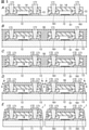
(4)弾性波装置の製造方法
次に、実施形態1に係る弾性波装置1の製造方法について、図4A~図4F及び図5A~図5Eを参照して説明する。実施形態1に係る弾性波装置1は、第1工程から第11工程により製造される。
(4) Manufacturing Method of Elastic Wave Device Next, the manufacturing method of the
第1工程では、図4Aに示すように、複数の弾性波装置1の基板11の元になるウェハ51を準備する。
In the first step, as shown in FIG. 4A, a
第2工程では、図4Bに示すように、ウェハ51上に、薄膜微細加工技術により、複数(図示例では2つ)のIDT電極12と複数(図示例では4つ)のパッド電極161とを形成する。
In the second step, as shown in FIG. 4B, a plurality of (two in the illustrated example)
第3工程では、図4Cに示すように、ウェハ51の上面の全面を覆うように樹脂を塗布し、複数のスペーサ層13の元になる樹脂膜52を形成する。
In the third step, as shown in FIG. 4C, the resin is applied so as to cover the entire upper surface of the
第4工程では、図4Dに示すように、フォトリソグラフィ法により樹脂膜52をパターニングして、複数(図示例では2つ)のスペーサ層13を形成する。第4工程では、樹脂膜52は加熱により硬化されていない。
In the fourth step, as shown in FIG. 4D, the
第5工程では、図4Eに示すように、ラミネート加工により、カバー部材14の元になる樹脂膜53をスペーサ層13上に形成する。樹脂膜53によって、スペーサ層13の貫通孔131が塞がれる。ラミネート加工を施した後、全体を加熱する。これによってスペーサ層13及びカバー部材14を硬化させる。その結果、カバー部材14とスペーサ層13とが接合され、IDT電極12が臨む空間S1が形成される。
In the fifth step, as shown in FIG. 4E, the
第6工程では、図4Fに示すように、レーザ加工等により、スペーサ層13及びカバー部材14を貫くように複数(図示例では4つ)の貫通孔54を形成する。これにより、複数のパッド電極161を露出させる。また、樹脂膜53がスペーサ層13の外周に沿うように、樹脂膜53のうち、隣接する2つのスペーサ層13間の部分を除去する。
In the sixth step, as shown in FIG. 4F, a plurality of (four in the illustrated example) through
第7工程では、図5Aに示すように、複数(図示例では4つ)の貫通ビア171を形成する。より詳細には、まず、シード層(下地膜)を形成する。次に、貫通ビア171が形成される箇所を露出するように、シード層に対してフォトマスクでパターニングを行い、レジスト膜を形成する。そして、シード層のうち露出している部分に対して、電解めっきによって貫通ビア171を形成する。その後、レジスト膜を除去し、さらに、除去したレジスト膜の下のシード層を除去する。
In the seventh step, as shown in FIG. 5A, a plurality of (four in the illustrated example) penetrating
第8工程では、図5Bに示すように、保護層15の元になる樹脂膜55を形成する。より詳細には、まず、ウェハ51の一部、スペーサ層13、カバー部材14、及び貫通ビア171を覆うように、樹脂膜55の元になる樹脂を塗布して硬化させる。次に、貫通ビア171が露出するまで、樹脂膜55を研削する。
In the eighth step, as shown in FIG. 5B, the
第9工程では、図5Cに示すように、貫通ビア171上に外部電極172を形成する。より詳細には、まず、シード層を形成する。次に、シード層の上に、外部電極172の位置が露出するように、シード層に対してフォトマスクでパターニングを行い、レジスト膜を形成する。そして、シード層のうち露出している部分に対して、電解めっきによって外部電極172を形成する。その後、レジスト膜を除去し、さらに、除去したレジスト膜の下のシード層を除去する。
In the ninth step, as shown in FIG. 5C, an
第10工程では、図5Dに示すように、弾性波装置1の端部となる領域において樹脂膜55の一部を除去する。より詳細には、樹脂膜55に対して、図5Dの矢印方向にレーザ光を照射してアブレーション加工を行う。上記領域において、位置ごとにレーザ光の狙い深度を変えることにより、樹脂膜55の表面が所定の形状になるように樹脂膜55の一部を除去する。
In the tenth step, as shown in FIG. 5D, a part of the
第11工程では、図5Eに示すように、ダイシング装置等により樹脂膜55及びウェハ51を切断する。これにより、複数(図示例では2つ)の弾性波装置1を得ることができる。
In the eleventh step, as shown in FIG. 5E, the
なお、上記製造方法は弾性波装置1の製造方法の一例であり、弾性波装置1は、他の製造方法を用いて製造してもよい。
The above manufacturing method is an example of the manufacturing method of the
(5)効果
以上説明したように、実施形態1に係る弾性波装置1では、基板11の厚さ方向D1において基板11から遠ざかるにつれて保護層15の側面155が内側に位置する。言い換えると、弾性波装置1では、保護層15における側面155において、側面155と第4主面154との交線156を含む部分は、基板11の厚さ方向D1からの平面視において、基板11の外縁113よりも内側に位置する。更に言い換えると、弾性波装置1では、保護層15の側面155のうちの少なくとも第4主面154側の部分は、厚さ方向D1からの平面視において、基板11の外縁よりも内側に位置する。すなわち、保護層15は、基板11の厚さ方向D1において先端部が凹んでいる。これにより、弾性波装置1を実装基板2に実装させる際に、弾性波装置1に対して実装基板2が傾いているとしても、弾性波装置1の角部が実装基板2に衝突すること(実装基板2への弾性波装置1の角あたり)を低減させることができる。その結果、クラックが発生しにくくすることができる。さらに、保護層15による封止性の低下を抑制することができる。
(5) Effect As described above, in the
実施形態1に係る弾性波装置1では、全周に亘って、基板11から遠ざかるにつれて保護層15の側面155が内側に位置する。言い換えると、保護層15の側面155は、保護層15の全周に亘って設けられており、かつ、側面155と第4主面154との交線156を含む部分は、基板11の外縁113よりも内側に位置する。更に言い換えると、保護層15の側面155は、保護層15の全周に亘って設けられており、かつ、側面155のうちの第4主面154側の部分は、基板11の外縁113よりも内側に位置する。これにより、弾性波装置1を実装基板2に実装させる際に、弾性波装置1に対して実装基板2がどのように傾いているとしても、弾性波装置1の角部が実装基板2に衝突することを低減できるので、保護層15にクラックが発生することを抑制できる。
In the
実施形態1に係る弾性波装置1では、スペーサ層13とカバー部材14と保護層15とを貫通する貫通ビア171が設けられている。これにより、基板11とスペーサ層13とカバー部材14とで囲まれた空間S1の気密性を高めることができるので、信頼性を向上させることができる。
In the
(6)変形例
以下、実施形態1の変形例について説明する。
(6) Modification Example The modification of the first embodiment will be described below.
弾性波装置1において、保護層15の領域152は、保護層15の全周に亘って設けられていることに限定されない。保護層15の領域152は、保護層15の少なくとも一部に設けられていればよい。
In the
弾性波装置1は、圧電基板である基板11に代えて、高音速支持基板と圧電膜とを備える構成であってもよい。この構成では、高音速支持基板上に圧電膜が設けられている。高音速支持基板は、圧電膜を伝搬する弾性波の音速より、伝搬する弾性波(バルク波)の音速が高速である基板である。
The
弾性波装置1は、基板11に代えて、高音速支持基板と低音速膜と圧電膜とを備える構成であってもよい。この構成では、高音速支持基板上に、低音速膜、圧電膜がこの順に設けられている。低音速膜は、圧電膜を伝搬する弾性波の音速より、伝搬する弾性波(バルク波)の音速が低速である膜である。
The
弾性波装置1は、基板11に代えて、支持基板と高音速膜と低音速膜と圧電膜とを備える構成であってもよい。この構成では、支持基板上に、高音速膜、低音速膜、圧電膜がこの順に積層されている。高音速膜は、圧電膜を伝搬する弾性波の音速より、伝搬する弾性波(バルク波)の音速が高速である膜である。
The
実施形態1及び上記の各変形例により、弾性波装置1は、少なくとも一部に圧電性を有する基板を備えていればよい。
According to the first embodiment and each of the above modifications, the
実施形態1では、保護層15の側面155のうちの第4主面154側の部分が、基板11の厚さ方向D1からの平面視において、基板11の外縁113よりも内側に位置するが、実施形態1の変形例として、保護層15の側面155の全てが、基板11の厚さ方向D1からの平面視において、基板11の外縁113よりも内側に位置してもよい。要するに、保護層15の側面155のうちの少なくとも第4主面154側の部分が、基板11の厚さ方向D1からの平面視において、基板11の外縁113よりも内側に位置すればよい。
In the first embodiment, the portion of the
上記の各変形例に係る弾性波装置1においても、実施形態1に係る弾性波装置1と同様の効果を奏する。
The
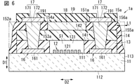
(実施形態2)
実施形態2に係る弾性波装置1aは、図6に示すようにパターン層18を備える点で、実施形態1に係る弾性波装置1(図1参照)と相違する。なお、実施形態2に係る弾性波装置1aに関し、実施形態1に係る弾性波装置1と同様の構成要素については、同一の符号を付して説明を省略する。
(Embodiment 2)
The
(1)弾性波装置の構成
弾性波装置1aは、図6に示すように、パターン層18と、保護レジスト層19とを備える。また、弾性波装置1aは、保護層15(図1参照)に代えて、保護層15aを備える。なお、弾性波装置1aは、実施形態1に係る弾性波装置1と同様、基板11と、IDT電極12と、スペーサ層13と、カバー部材14と、配線層16と、外部接続電極17とを備える。
(1) Configuration of Elastic Wave Device The
パターン層18は、カバー部材14の第2主面142上に設けられている。パターン層18は、例えば、インダクタ又はキャパシタを含むリアクタンス素子を構成する。パターン層18は、IDT電極12と電気的に接続されていてもよいし、IDT電極12とは電気的に独立して設けられていてもよい。
The
保護層15aは、保護層15と同様、中央領域151aと、中央領域151aの周囲に位置する領域152aとを有する。また、保護層15aは、実施形態1の保護層15と同様、第3主面153aと、第4主面154aと、側面155aとを有する。第3主面153aは、第2主面142と接する。第4主面154aは、基板11の厚さ方向D1において、第3主面153aと対向する。側面155aは、第4主面154aに連なる。言い換えると、側面155aは、第4主面154aの周囲から基板11側に向かって設けられている。なお、実施形態2の保護層15aに関し、実施形態1の保護層15と同様の構成及び機能については説明を省略する。
Like the
保護層15aの中央領域151aでは、パターン層18が露出するようにパターン層18が形成されている箇所が貫通している。
In the
保護層15aの領域152aでは、保護層15の領域152と同様、基板11の厚さ方向D1において基板11から遠ざかるにつれて、厚さ方向D1と直交する方向D2において保護層15aの側面155aと基板11の外縁113との間の距離L1が長くなる。言い換えると、保護層15aにおける側面155aにおいて、側面155aと第4主面154aとの交線156aを含む部分は、基板11の厚さ方向D1からの平面視において、基板11の外縁113よりも内側に位置する。更に言い換えると、保護層15aの側面155aのうちの第4主面154a側の部分は、厚さ方向D1からの平面視において、基板11の外縁113よりも内側に位置する。
In the
保護レジスト層19は、保護層15a上に設けられている。保護レジスト層19は、外部接続電極17の外部電極172の少なくとも一部が露出するように貫通孔191を有する。保護レジスト層19は、方向D2において、保護層15aよりも突出しないように形成されている。保護レジスト層19は、外部電極172にはんだが設けられる際に、はんだの濡れ広がりを低減させるために設けられている。
The protective resist
(2)弾性波装置の製造方法
次に、実施形態2に係る弾性波装置1aの製造方法について説明する。実施形態2に係る弾性波装置1aは、第1工程から第12工程により製造される。実施形態1に係る弾性波装置1の製造方法と同様の箇所については、適宜説明を省略する。
(2) Manufacturing Method of Elastic Wave Device Next, a manufacturing method of the
第1工程では、複数の弾性波装置1aの基板11の元になるウェハを準備する。
In the first step, a wafer that is the basis of the
第2工程では、ウェハ上に、複数のIDT電極12と複数のパッド電極161とを形成する。
In the second step, a plurality of
第3工程では、ウェハの上面の全面を覆うように樹脂を塗布し、複数のスペーサ層13の元になる樹脂膜を形成する。 In the third step, the resin is applied so as to cover the entire upper surface of the wafer to form a resin film that is the basis of the plurality of spacer layers 13.
第4工程では、上記樹脂層をパターニングして、複数のスペーサ層13を形成する。 In the fourth step, the resin layer is patterned to form a plurality of spacer layers 13.
第5工程では、ラミネート加工により、カバー部材14の元になる樹脂膜をスペーサ層13上に形成する。上記樹脂膜によって、スペーサ層13の貫通孔131が塞がれる。ラミネート加工を施した後、全体を加熱する。
In the fifth step, a resin film that is the basis of the
第6工程では、スペーサ層13及びカバー部材14を貫くように複数の貫通孔を形成する。また、上記樹脂膜がスペーサ層13の外周に沿うように、上記樹脂膜のうち、隣接する2つのスペーサ層13間の部分を除去する。
In the sixth step, a plurality of through holes are formed so as to penetrate the
第7工程では、複数の貫通ビア171及びパターン層18を形成する。より詳細には、まず、シード層を形成する。次に、貫通ビア171及びパターン層18が形成される箇所を露出するように、シード層に対してフォトマスクでパターニングを行い、レジスト膜を形成する。そして、第6工程で形成した貫通孔に貫通ビア171を形成する。また、カバー部材14の第2主面142にパターン層18を形成する。その後、レジスト膜を除去し、さらに、除去したレジスト膜の下のシード層を除去する。
In the seventh step, a plurality of penetrating
第8工程では、保護層15aの元になる樹脂膜を形成する。より詳細には、まず、ウェハの一部、スペーサ層13、カバー部材14、貫通ビア171を覆うように、上記樹脂膜の元になる樹脂を塗布して硬化させる。次に、貫通ビア171が露出するまで、上記樹脂膜を研削する。
In the eighth step, the resin film that is the basis of the
第9工程では、貫通ビア171上に外部電極172を形成する。
In the ninth step, the
第10工程では、保護層15a及び外部電極172の上に、保護レジスト層19の元になるレジスト膜を形成する。より詳細には、まず、シード層を形成し、次に、外部電極172の一部が露出するように、シード層に対してフォトマスクでパターニングを行い、レジスト膜を形成する。
In the tenth step, a resist film that is the basis of the protective resist
第11工程では、弾性波装置1aの端部となる領域において第8工程で形成された樹脂膜及び第10工程で形成されたレジスト膜の一部を除去する。より詳細には、樹脂膜及びレジスト膜に対してレーザ光を照射してアブレーション加工を行う。上記領域において、位置ごとにレーザ光の狙い深度を変えることにより、樹脂膜及びレジスト膜の表面が所定の形状になるように樹脂膜の一部及びレジスト膜の一部を除去する。
In the eleventh step, a part of the resin film formed in the eighth step and the resist film formed in the tenth step is removed in the region to be the end of the
第12工程では、ダイシング装置等により樹脂膜及びウェハを切断する。これにより、複数の弾性波装置1aを得ることができる。
In the twelfth step, the resin film and the wafer are cut by a dicing device or the like. Thereby, a plurality of
なお、上記製造方法は弾性波装置1aの製造方法の一例であり、弾性波装置1aは、他の製造方法を用いて製造してもよい。
The above manufacturing method is an example of the manufacturing method of the
(3)効果
以上説明したように、実施形態2に係る弾性波装置1aによれば、パターン層18を一体にすることができるので、パターン層18が追加されても大型化を低減させることができる。
(3) Effect As described above, according to the
(4)変形例
以下、実施形態2の変形例について説明する。
(4) Modification Example The modification of the second embodiment will be described below.
実施形態2の変形例として、実施形態1の変形例と同様、弾性波装置1aは、基板11に代えて、高音速支持基板と圧電膜とを備える構成であってもよい。あるいは、弾性波装置1aは、基板11に代えて、高音速支持基板と低音速膜と圧電膜とを備える構成であってもよいし、支持基板と高音速膜と低音速膜と圧電膜とを備える構成であってもよい。
As a modification of the second embodiment, as in the modification of the first embodiment, the
実施形態2では、保護層15aの側面155aのうちの第4主面154a側の部分が、基板11の厚さ方向D1からの平面視において、基板11の外縁113よりも内側に位置するが、実施形態2の変形例として、保護層15aの側面155aの全てが、基板11の厚さ方向D1からの平面視において、基板11の外縁113よりも内側に位置してもよい。要するに、保護層15aの側面155aのうちの少なくとも第4主面154a側の部分が、基板11の厚さ方向D1からの平面視において、基板11の外縁113よりも内側に位置すればよい。
In the second embodiment, the portion of the
上記の各変形例に係る弾性波装置1aにおいても、実施形態2に係る弾性波装置1aと同様の効果を奏する。
The
以上説明した実施形態及び変形例は、本発明の様々な実施形態及び変形例の一部に過ぎない。また、実施形態及び変形例は、本発明の目的を達成できれば、設計等に応じて種々の変更が可能である。 The embodiments and modifications described above are only a part of various embodiments and modifications of the present invention. Further, the embodiments and modifications can be variously modified according to the design and the like as long as the object of the present invention can be achieved.
(まとめ)
以上説明した実施形態及び変形例より以下の態様が開示されている。
(summary)
The following embodiments are disclosed from the embodiments and modifications described above.
第1態様に係る弾性波装置(1;1a)は、基板(11)と、IDT電極(12)と、スペーサ層(13)と、カバー部材(14)と、保護層(15;15a)とを備える。基板(11)は、少なくとも一部に圧電性を有する。IDT電極(12)は、基板(11)上に設けられている。スペーサ層(13)は、基板(11)上に設けられており、かつ、IDT電極(12)を囲んでいる。カバー部材(14)は、スペーサ層(13)上に設けられており、IDT電極(12)から離れている。カバー部材(14)は、スペーサ層(13)側の第1主面(141)と、第1主面(141)と対向する第2主面(142)とを有する。保護層(15;15a)は、カバー部材(14)上に設けられており、第2主面(142)と接する第3主面(153;153a)と、第3主面(153;153a)と対向する第4主面(154;154a)と、第4主面(154;154a)に連なる側面(155;155a)とを有する。保護層(15;15a)における側面(155;155a)のうちの少なくとも一部において、側面(155;155a)と第4主面(154;154a)との交線(156;156a)を含む部分は、基板(11)の厚さ方向(D1)からの平面視において、基板(11)の外縁(113)よりも内側に位置する。 The elastic wave device (1; 1a) according to the first aspect includes a substrate (11), an IDT electrode (12), a spacer layer (13), a cover member (14), and a protective layer (15; 15a). To prepare for. The substrate (11) has at least a part of piezoelectricity. The IDT electrode (12) is provided on the substrate (11). The spacer layer (13) is provided on the substrate (11) and surrounds the IDT electrode (12). The cover member (14) is provided on the spacer layer (13) and is separated from the IDT electrode (12). The cover member (14) has a first main surface (141) on the spacer layer (13) side and a second main surface (142) facing the first main surface (141). The protective layer (15; 15a) is provided on the cover member (14), and has a third main surface (153; 153a) in contact with the second main surface (142) and a third main surface (153; 153a). It has a fourth main surface (154; 154a) facing the surface and a side surface (155; 155a) connected to the fourth main surface (154; 154a). At least a part of the side surface (155; 155a) in the protective layer (15; 15a) including the line of intersection (156; 156a) between the side surface (155; 155a) and the fourth main surface (154; 154a). Is located inside the outer edge (113) of the substrate (11) in a plan view from the thickness direction (D1) of the substrate (11).
第1の態様に係る弾性波装置(1;1a)によれば、保護層(15;15a)の側面(155;155a)のうちの少なくとも一部において、側面(155;155a)と第4主面(154;154a)との交線(156;156a)を含む部分が基板(11)の外縁(113)よりも内側に位置する。すなわち、保護層(15;15a)は、基板(11)の厚さ方向(D1)において先端部が凹んでいる。これにより、弾性波装置(1;1a)を実装基板(2)に実装させる際に、弾性波装置(1;1a)に対して実装基板(2)が傾いているとしても、弾性波装置(1;1a)の角部が実装基板(2)に衝突することを低減させることができる。その結果、クラックが発生しにくくすることができる。さらに、保護層(15;15a)による封止性の低下を抑制することができる。 According to the elastic wave device (1; 1a) according to the first aspect, at least a part of the side surface (155; 155a) of the protective layer (15; 15a) has a side surface (155; 155a) and a fourth main. The portion including the line of intersection (156; 156a) with the surface (154; 154a) is located inside the outer edge (113) of the substrate (11). That is, the protective layer (15; 15a) has a recessed tip in the thickness direction (D1) of the substrate (11). As a result, when the elastic wave device (1; 1a) is mounted on the mounting substrate (2), even if the mounting substrate (2) is tilted with respect to the elastic wave device (1; 1a), the elastic wave device (1; 1a) is mounted. It is possible to reduce the collision of the corners of 1; 1a) with the mounting substrate (2). As a result, cracks can be less likely to occur. Further, it is possible to suppress the deterioration of the sealing property due to the protective layer (15; 15a).
第2の態様に係る弾性波装置(1;1a)では、第1の態様において、保護層(15;15a)の側面(155;155a)は、保護層(15;15a)の全周に亘って設けられており、かつ、側面(155;155a)と第4主面(154;154a)との交線(156;156a)を含む部分は、厚さ方向(D1)からの平面視において、基板(11)の外縁(113)よりも内側に位置する。 In the elastic wave device (1; 1a) according to the second aspect, in the first aspect, the side surface ( 155 ; 155a ) of the protective layer (15; 15a) extends over the entire circumference of the protective layer (15; 15a). The portion including the line of intersection (156; 156a) between the side surface (155; 155a) and the fourth main surface (154; 154a) is in the plan view from the thickness direction (D1). It is located inside the outer edge (113) of the substrate (11).
第2の態様に係る弾性波装置(1;1a)によれば、弾性波装置(1;1a)を実装基板(2)に実装させる際に、弾性波装置(1;1a)に対して実装基板(2)がどのように傾いているとしても、弾性波装置(1;1a)の角部が実装基板(2)に衝突することを低減できるので、保護層(15;15a)にクラックが発生することを抑制できる。 According to the elastic wave device (1; 1a) according to the second aspect, when the elastic wave device (1; 1a) is mounted on the mounting substrate (2), it is mounted on the elastic wave device (1; 1a). No matter how the substrate (2) is tilted, it is possible to reduce the collision of the corners of the elastic wave device (1; 1a) with the mounting substrate (2), so that the protective layer (15; 15a) has cracks. It can be suppressed from occurring.
第3の態様に係る弾性波装置(1;1a)は、第1又は2の態様において、外部接続電極(17)を更に備える。外部接続電極(17)は、IDT電極(12)に電気的に接続されている。外部接続電極(17)は、貫通ビア(171)を含む。貫通ビア(171)は、スペーサ層(13)とカバー部材(14)と保護層(15;15a)とを貫通する。 The elastic wave device (1; 1a) according to the third aspect further includes an external connection electrode (17) in the first or second aspect. The external connection electrode (17) is electrically connected to the IDT electrode (12). The external connection electrode (17) includes a through via (171). The penetrating via (171) penetrates the spacer layer (13), the cover member (14), and the protective layer (15; 15a).
第3の態様に係る弾性波装置(1;1a)によれば、基板(11)とスペーサ層(13)とカバー部材(14)とで囲まれた空間(S1)の気密性を高めることができるので、信頼性を向上させることができる。 According to the elastic wave device (1; 1a) according to the third aspect, the airtightness of the space (S1) surrounded by the substrate (11), the spacer layer (13), and the cover member (14) can be enhanced. Since it can be done, reliability can be improved.
第4の態様に係る弾性波装置(1a)は、第1~3の態様のいずれか1つにおいて、パターン層(18)を更に備える。パターン層(18)は、保護層(15;15a)の内部に設けられている。 The elastic wave device (1a) according to the fourth aspect further includes a pattern layer (18) in any one of the first to third aspects. The pattern layer (18) is provided inside the protective layer (15; 15a).
第4の態様に係る弾性波装置(1a)によれば、パターン層(18)を一体にすることができるので、パターン層(18)が追加されても大型化を低減させることができる。 According to the elastic wave device (1a) according to the fourth aspect, since the pattern layer (18) can be integrated, it is possible to reduce the increase in size even if the pattern layer (18) is added.
1,1a 弾性波装置
11 基板
111 主面
112 主面
113 外縁
12 IDT電極
121 電極指
13 スペーサ層
131 貫通孔
14 カバー部材
141 第1主面
142 第2主面
15,15a 保護層
151,151a 中央領域
152,152a 領域
153,153a 第3主面
154,154a 第4主面
155,155a 側面
156,156a 交線
16 配線層
161 パッド電極
17 外部接続電極
171 貫通ビア
172 外部電極
18 パターン層
19 保護レジスト層
191 貫通孔
2 実装基板
21 端子
3 電子部品モジュール
4 実装ノズル
41 吸引孔
51 ウェハ
52 樹脂膜
53 樹脂膜
54 貫通孔
55 樹脂膜
D1 厚さ方向
D2 方向
L1 距離
S1 空間
1,1a
Claims (3)
前記基板上に設けられているIDT電極と、
前記基板上に設けられており、かつ、前記IDT電極を囲んでいるスペーサ層と、
前記スペーサ層上に設けられており、前記IDT電極から離れており、かつ、前記スペーサ層側の第1主面と、前記第1主面と対向する第2主面とを有するカバー部材と、
前記カバー部材上に設けられており、前記第2主面と接する第3主面と、前記第3主面と対向する第4主面と、前記第4主面に連なる側面とを有する保護層と、
前記IDT電極に電気的に接続されている外部接続電極と、を備え、
前記外部接続電極は、前記スペーサ層と前記カバー部材と前記保護層とを貫通する貫通ビアを含み、
前記保護層における前記側面のうちの少なくとも一部において、前記側面と前記第4主面との交線は、前記基板の厚さ方向からの平面視において、前記第4主面と前記基板との間であって前記基板と平行な任意の仮想平面と前記側面との交線よりも内側に位置する、
弾性波装置。 With a substrate that has piezoelectricity at least in part,
The IDT electrode provided on the substrate and
A spacer layer provided on the substrate and surrounding the IDT electrode, and
A cover member provided on the spacer layer, separated from the IDT electrode, and having a first main surface on the spacer layer side and a second main surface facing the first main surface.
A protective layer provided on the cover member and having a third main surface in contact with the second main surface, a fourth main surface facing the third main surface, and a side surface connected to the fourth main surface. And ,
An external connection electrode electrically connected to the IDT electrode is provided.
The external connection electrode includes a penetrating via that penetrates the spacer layer, the cover member, and the protective layer.
In at least a part of the side surface of the protective layer, the line of intersection between the side surface and the fourth main surface is a plan view of the substrate from the thickness direction of the fourth main surface and the substrate. Located inside the line of intersection of any virtual plane parallel to the substrate and the side surface between them.
Elastic wave device.
請求項1に記載の弾性波装置。 The side surface of the protective layer is provided over the entire circumference of the protective layer, and the line of intersection between the side surface and the fourth main surface is the first in a plan view from the thickness direction. 4 Located between the main surface and the substrate and inside the line of intersection of any virtual plane parallel to the substrate and the side surface.
The elastic wave device according to claim 1.
請求項1又は2に記載の弾性波装置。 The elastic wave device according to claim 1 or 2.
Priority Applications (3)
| Application Number | Priority Date | Filing Date | Title |
|---|---|---|---|
| KR1020180148303A KR102163886B1 (en) | 2017-12-19 | 2018-11-27 | Elastic wave device |
| US16/202,382 US11533038B2 (en) | 2017-12-19 | 2018-11-28 | Elastic wave device |
| CN201811559899.5A CN110034741B (en) | 2017-12-19 | 2018-12-19 | Elastic wave device |
Applications Claiming Priority (2)
| Application Number | Priority Date | Filing Date | Title |
|---|---|---|---|
| JP2017243232 | 2017-12-19 | ||
| JP2017243232 | 2017-12-19 |
Publications (2)
| Publication Number | Publication Date |
|---|---|
| JP2019110519A JP2019110519A (en) | 2019-07-04 |
| JP6996467B2 true JP6996467B2 (en) | 2022-01-17 |
Family
ID=67180295
Family Applications (1)
| Application Number | Title | Priority Date | Filing Date |
|---|---|---|---|
| JP2018187860A Active JP6996467B2 (en) | 2017-12-19 | 2018-10-03 | Elastic wave device |
Country Status (2)
| Country | Link |
|---|---|
| JP (1) | JP6996467B2 (en) |
| CN (1) | CN110034741B (en) |
Families Citing this family (2)
| Publication number | Priority date | Publication date | Assignee | Title |
|---|---|---|---|---|
| CN114342098B (en) * | 2019-09-12 | 2025-02-25 | 株式会社村田制作所 | Piezoelectric elements |
| JP7654475B2 (en) * | 2021-06-11 | 2025-04-01 | 太陽誘電株式会社 | Electronic component and method for manufacturing electronic component |
Citations (3)
| Publication number | Priority date | Publication date | Assignee | Title |
|---|---|---|---|---|
| JP2008182292A (en) | 2007-01-23 | 2008-08-07 | Fujitsu Media Device Kk | Elastic wave device |
| JP2016066989A (en) | 2014-09-19 | 2016-04-28 | 日本電波工業株式会社 | Piezoelectric device and manufacturing method thereof |
| JP2016123020A (en) | 2014-12-25 | 2016-07-07 | 京セラ株式会社 | Elastic wave device and communication device |
Family Cites Families (5)
| Publication number | Priority date | Publication date | Assignee | Title |
|---|---|---|---|---|
| JP4210958B2 (en) * | 2004-07-14 | 2009-01-21 | 株式会社村田製作所 | Piezoelectric device |
| JP4585419B2 (en) * | 2005-10-04 | 2010-11-24 | 富士通メディアデバイス株式会社 | Surface acoustic wave device and manufacturing method thereof |
| JP5755434B2 (en) * | 2010-11-30 | 2015-07-29 | 京セラ株式会社 | Elastic wave device and manufacturing method thereof |
| WO2014151417A1 (en) * | 2013-03-15 | 2014-09-25 | Cornell University | Low-power acoustic data acquisition system and methods |
| JP6288110B2 (en) * | 2013-12-27 | 2018-03-07 | 株式会社村田製作所 | Elastic wave device |
-
2018
- 2018-10-03 JP JP2018187860A patent/JP6996467B2/en active Active
- 2018-12-19 CN CN201811559899.5A patent/CN110034741B/en active Active
Patent Citations (3)
| Publication number | Priority date | Publication date | Assignee | Title |
|---|---|---|---|---|
| JP2008182292A (en) | 2007-01-23 | 2008-08-07 | Fujitsu Media Device Kk | Elastic wave device |
| JP2016066989A (en) | 2014-09-19 | 2016-04-28 | 日本電波工業株式会社 | Piezoelectric device and manufacturing method thereof |
| JP2016123020A (en) | 2014-12-25 | 2016-07-07 | 京セラ株式会社 | Elastic wave device and communication device |
Also Published As
| Publication number | Publication date |
|---|---|
| CN110034741B (en) | 2023-07-21 |
| CN110034741A (en) | 2019-07-19 |
| JP2019110519A (en) | 2019-07-04 |
Similar Documents
| Publication | Publication Date | Title |
|---|---|---|
| CN109075768B (en) | Elastic wave device and method for manufacturing same | |
| US20060192462A1 (en) | Piezoelectirc device | |
| US10707830B2 (en) | Elastic wave device and method for manufacturing the same | |
| US11165390B2 (en) | Piezoelectric resonator device | |
| JP2019106698A (en) | Electronic component module | |
| KR102163886B1 (en) | Elastic wave device | |
| KR102320449B1 (en) | Acoustic wave device and electronic component module | |
| JPWO2006001125A1 (en) | Piezoelectric device | |
| JP6963445B2 (en) | Electronic components | |
| CN105814796A (en) | Elastic wave filter device | |
| JP6996467B2 (en) | Elastic wave device | |
| JP6950658B2 (en) | Elastic wave device | |
| JP2021027383A (en) | Elastic wave device | |
| JP2013070347A (en) | Acoustic wave device and method of manufacturing the same | |
| KR102295454B1 (en) | Electronic components and modules having the same | |
| JP2008113178A (en) | Hollow sealing element and manufacturing method thereof | |
| JP2014230079A (en) | Surface acoustic wave device | |
| JP7042195B2 (en) | Electronic components and manufacturing methods for electronic components | |
| JP2007027211A (en) | Electronic component and manufacturing method thereof | |
| JP2015012428A (en) | Acoustic wave device, electronic component module, and mobile terminal | |
| JP2013197921A (en) | Manufacturing method of electronic component and electronic component | |
| JP2011109481A (en) | Surface acoustic wave device and method of manufacturing the same | |
| JP6068220B2 (en) | Manufacturing method of electronic parts | |
| JP6352844B2 (en) | Multi-circuit circuit board and surface acoustic wave device | |
| JP2014165287A (en) | Electronic component |
Legal Events
| Date | Code | Title | Description |
|---|---|---|---|
| A521 | Request for written amendment filed |
Free format text: JAPANESE INTERMEDIATE CODE: A523 Effective date: 20181029 |
|
| A621 | Written request for application examination |
Free format text: JAPANESE INTERMEDIATE CODE: A621 Effective date: 20200413 |
|
| A977 | Report on retrieval |
Free format text: JAPANESE INTERMEDIATE CODE: A971007 Effective date: 20210216 |
|
| A131 | Notification of reasons for refusal |
Free format text: JAPANESE INTERMEDIATE CODE: A131 Effective date: 20210224 |
|
| A521 | Request for written amendment filed |
Free format text: JAPANESE INTERMEDIATE CODE: A523 Effective date: 20210426 |
|
| A131 | Notification of reasons for refusal |
Free format text: JAPANESE INTERMEDIATE CODE: A131 Effective date: 20210615 |
|
| A521 | Request for written amendment filed |
Free format text: JAPANESE INTERMEDIATE CODE: A523 Effective date: 20210802 |
|
| TRDD | Decision of grant or rejection written | ||
| A01 | Written decision to grant a patent or to grant a registration (utility model) |
Free format text: JAPANESE INTERMEDIATE CODE: A01 Effective date: 20211116 |
|
| A61 | First payment of annual fees (during grant procedure) |
Free format text: JAPANESE INTERMEDIATE CODE: A61 Effective date: 20211129 |
|
| R150 | Certificate of patent or registration of utility model |
Ref document number: 6996467 Country of ref document: JP Free format text: JAPANESE INTERMEDIATE CODE: R150 |