JP6992062B2 - Laser power controller - Google Patents
Laser power controller Download PDFInfo
- Publication number
- JP6992062B2 JP6992062B2 JP2019521182A JP2019521182A JP6992062B2 JP 6992062 B2 JP6992062 B2 JP 6992062B2 JP 2019521182 A JP2019521182 A JP 2019521182A JP 2019521182 A JP2019521182 A JP 2019521182A JP 6992062 B2 JP6992062 B2 JP 6992062B2
- Authority
- JP
- Japan
- Prior art keywords
- value
- laser diode
- logical
- burst
- output
- Prior art date
- Legal status (The legal status is an assumption and is not a legal conclusion. Google has not performed a legal analysis and makes no representation as to the accuracy of the status listed.)
- Active
Links
Images


Classifications
-
- H—ELECTRICITY
- H04—ELECTRIC COMMUNICATION TECHNIQUE
- H04B—TRANSMISSION
- H04B10/00—Transmission systems employing electromagnetic waves other than radio-waves, e.g. infrared, visible or ultraviolet light, or employing corpuscular radiation, e.g. quantum communication
- H04B10/50—Transmitters
- H04B10/564—Power control
-
- H—ELECTRICITY
- H01—ELECTRIC ELEMENTS
- H01S—DEVICES USING THE PROCESS OF LIGHT AMPLIFICATION BY STIMULATED EMISSION OF RADIATION [LASER] TO AMPLIFY OR GENERATE LIGHT; DEVICES USING STIMULATED EMISSION OF ELECTROMAGNETIC RADIATION IN WAVE RANGES OTHER THAN OPTICAL
- H01S3/00—Lasers, i.e. devices using stimulated emission of electromagnetic radiation in the infrared, visible or ultraviolet wave range
- H01S3/005—Optical devices external to the laser cavity, specially adapted for lasers, e.g. for homogenisation of the beam or for manipulating laser pulses, e.g. pulse shaping
- H01S3/0085—Modulating the output, i.e. the laser beam is modulated outside the laser cavity
-
- H—ELECTRICITY
- H01—ELECTRIC ELEMENTS
- H01S—DEVICES USING THE PROCESS OF LIGHT AMPLIFICATION BY STIMULATED EMISSION OF RADIATION [LASER] TO AMPLIFY OR GENERATE LIGHT; DEVICES USING STIMULATED EMISSION OF ELECTROMAGNETIC RADIATION IN WAVE RANGES OTHER THAN OPTICAL
- H01S3/00—Lasers, i.e. devices using stimulated emission of electromagnetic radiation in the infrared, visible or ultraviolet wave range
- H01S3/10—Controlling the intensity, frequency, phase, polarisation or direction of the emitted radiation, e.g. switching, gating, modulating or demodulating
- H01S3/10007—Controlling the intensity, frequency, phase, polarisation or direction of the emitted radiation, e.g. switching, gating, modulating or demodulating in optical amplifiers
- H01S3/10015—Controlling the intensity, frequency, phase, polarisation or direction of the emitted radiation, e.g. switching, gating, modulating or demodulating in optical amplifiers by monitoring or controlling, e.g. attenuating, the input signal
-
- H—ELECTRICITY
- H01—ELECTRIC ELEMENTS
- H01S—DEVICES USING THE PROCESS OF LIGHT AMPLIFICATION BY STIMULATED EMISSION OF RADIATION [LASER] TO AMPLIFY OR GENERATE LIGHT; DEVICES USING STIMULATED EMISSION OF ELECTROMAGNETIC RADIATION IN WAVE RANGES OTHER THAN OPTICAL
- H01S3/00—Lasers, i.e. devices using stimulated emission of electromagnetic radiation in the infrared, visible or ultraviolet wave range
- H01S3/10—Controlling the intensity, frequency, phase, polarisation or direction of the emitted radiation, e.g. switching, gating, modulating or demodulating
- H01S3/10038—Amplitude control
-
- H—ELECTRICITY
- H01—ELECTRIC ELEMENTS
- H01S—DEVICES USING THE PROCESS OF LIGHT AMPLIFICATION BY STIMULATED EMISSION OF RADIATION [LASER] TO AMPLIFY OR GENERATE LIGHT; DEVICES USING STIMULATED EMISSION OF ELECTROMAGNETIC RADIATION IN WAVE RANGES OTHER THAN OPTICAL
- H01S3/00—Lasers, i.e. devices using stimulated emission of electromagnetic radiation in the infrared, visible or ultraviolet wave range
- H01S3/10—Controlling the intensity, frequency, phase, polarisation or direction of the emitted radiation, e.g. switching, gating, modulating or demodulating
- H01S3/13—Stabilisation of laser output parameters, e.g. frequency or amplitude
- H01S3/1306—Stabilisation of the amplitude
-
- H—ELECTRICITY
- H01—ELECTRIC ELEMENTS
- H01S—DEVICES USING THE PROCESS OF LIGHT AMPLIFICATION BY STIMULATED EMISSION OF RADIATION [LASER] TO AMPLIFY OR GENERATE LIGHT; DEVICES USING STIMULATED EMISSION OF ELECTROMAGNETIC RADIATION IN WAVE RANGES OTHER THAN OPTICAL
- H01S5/00—Semiconductor lasers
- H01S5/005—Optical components external to the laser cavity, specially adapted therefor, e.g. for homogenisation or merging of the beams or for manipulating laser pulses, e.g. pulse shaping
- H01S5/0085—Optical components external to the laser cavity, specially adapted therefor, e.g. for homogenisation or merging of the beams or for manipulating laser pulses, e.g. pulse shaping for modulating the output, i.e. the laser beam is modulated outside the laser cavity
-
- H—ELECTRICITY
- H01—ELECTRIC ELEMENTS
- H01S—DEVICES USING THE PROCESS OF LIGHT AMPLIFICATION BY STIMULATED EMISSION OF RADIATION [LASER] TO AMPLIFY OR GENERATE LIGHT; DEVICES USING STIMULATED EMISSION OF ELECTROMAGNETIC RADIATION IN WAVE RANGES OTHER THAN OPTICAL
- H01S5/00—Semiconductor lasers
- H01S5/04—Processes or apparatus for excitation, e.g. pumping, e.g. by electron beams
- H01S5/042—Electrical excitation ; Circuits therefor
- H01S5/0427—Electrical excitation ; Circuits therefor for applying modulation to the laser
-
- H—ELECTRICITY
- H01—ELECTRIC ELEMENTS
- H01S—DEVICES USING THE PROCESS OF LIGHT AMPLIFICATION BY STIMULATED EMISSION OF RADIATION [LASER] TO AMPLIFY OR GENERATE LIGHT; DEVICES USING STIMULATED EMISSION OF ELECTROMAGNETIC RADIATION IN WAVE RANGES OTHER THAN OPTICAL
- H01S5/00—Semiconductor lasers
- H01S5/06—Arrangements for controlling the laser output parameters, e.g. by operating on the active medium
- H01S5/068—Stabilisation of laser output parameters
- H01S5/0683—Stabilisation of laser output parameters by monitoring the optical output parameters
- H01S5/06832—Stabilising during amplitude modulation
-
- H—ELECTRICITY
- H01—ELECTRIC ELEMENTS
- H01S—DEVICES USING THE PROCESS OF LIGHT AMPLIFICATION BY STIMULATED EMISSION OF RADIATION [LASER] TO AMPLIFY OR GENERATE LIGHT; DEVICES USING STIMULATED EMISSION OF ELECTROMAGNETIC RADIATION IN WAVE RANGES OTHER THAN OPTICAL
- H01S5/00—Semiconductor lasers
- H01S5/06—Arrangements for controlling the laser output parameters, e.g. by operating on the active medium
- H01S5/068—Stabilisation of laser output parameters
- H01S5/0683—Stabilisation of laser output parameters by monitoring the optical output parameters
- H01S5/06835—Stabilising during pulse modulation or generation
-
- H—ELECTRICITY
- H04—ELECTRIC COMMUNICATION TECHNIQUE
- H04B—TRANSMISSION
- H04B10/00—Transmission systems employing electromagnetic waves other than radio-waves, e.g. infrared, visible or ultraviolet light, or employing corpuscular radiation, e.g. quantum communication
- H04B10/50—Transmitters
- H04B10/501—Structural aspects
- H04B10/503—Laser transmitters
-
- H—ELECTRICITY
- H01—ELECTRIC ELEMENTS
- H01S—DEVICES USING THE PROCESS OF LIGHT AMPLIFICATION BY STIMULATED EMISSION OF RADIATION [LASER] TO AMPLIFY OR GENERATE LIGHT; DEVICES USING STIMULATED EMISSION OF ELECTROMAGNETIC RADIATION IN WAVE RANGES OTHER THAN OPTICAL
- H01S5/00—Semiconductor lasers
- H01S5/06—Arrangements for controlling the laser output parameters, e.g. by operating on the active medium
- H01S5/068—Stabilisation of laser output parameters
- H01S5/06812—Stabilisation of laser output parameters by monitoring or fixing the threshold current or other specific points of the L-I or V-I characteristics
Description
光ファイバ通信システムにおいては、送信レーザダイオードの出力パワーを制御できることが多くの理由で重要である。第一に、損傷を避けるため、レーザの平均およびピークパワーは一定の限界を超えてはならない。第二に、バイナリ(または他の基数)データ値に対応する異なるパワーレベルは、リンクの端での確実な受信を保証するために、変調指数(或いは消光比として定義される)が全体システム仕様内になるように設定されなければならない。任意の制御システムに対処する一つの難しさは、レーザの特性が、温度とともに、また経年変化によって、さらには理想的な線形応答からの逸脱によっても大きく変化する可能性があり、そのため、「ハイ」および「ロー」の駆動電流レベルについての従来の工場セットアップが十分ではない、ということである。 In fiber optic communication systems, the ability to control the output power of a transmitting laser diode is important for many reasons. First, the average and peak power of the laser should not exceed certain limits to avoid damage. Second, different power levels corresponding to binary (or other radix) data values have a modulation index (or defined as the extinction ratio) overall system specification to ensure reliable reception at the end of the link. Must be set to be inside. One difficulty dealing with any control system is that the properties of the laser can change significantly with temperature, over time, and even with deviations from the ideal linear response, and therefore "high". The traditional factory setup for "low" drive current levels is not sufficient.
従来技術には、最小および最大送信光出力の瞬時値を推定し、デバイス特性の変化を補償することを目的とした方法を説明する多数の技術が存在する。モニタダイオードおよびそれに関連する回路の帯域幅が制限されているため、大部分はその有効性が限定されている。 There are numerous prior art techniques that describe methods aimed at estimating the instantaneous values of the minimum and maximum transmitted light outputs and compensating for changes in device characteristics. Due to the limited bandwidth of the monitor diode and its associated circuits, its effectiveness is largely limited.
送信された出力パワーを監視することは、データを一連の離散的なバーストで送信する光通信リンクではさらに困難であり、その理由は、光出力の平均値は大きく変動する可能性があり、また、最小レベルおよび最大レベルの適切な推定値に達するために先行技術に記載されている殆どの方法にとって瞬間レベルは十分に安定していないためである。温度に関連する影響はさらに深刻である可能性が高く、その理由は、送信レーザダイオードはデータバーストのために活性化される前に長期間オフ状態にあり得、それ故に、データバーストの間に昇温する前に周囲温度に冷却され得るためである。 Monitoring the transmitted output power is even more difficult with optical communication links that transmit data in a series of discrete bursts, because the average value of the optical output can fluctuate significantly. This is because the instantaneous level is not stable enough for most of the methods described in the prior art to reach the appropriate estimates of the minimum and maximum levels. The temperature-related effects are likely to be even more severe, because the transmitting laser diode can be off for a long time before being activated for a data burst, and therefore during the data burst. This is because it can be cooled to the ambient temperature before the temperature rises.
したがって、データバースト中に論理「1」および論理「0」に対応する最小および最大の光出力をほぼ連続的に検知できることが望ましい。さらに、適度な帯域幅だけで送信パワーモニタ機能を使用すると共に、送信データペイロードを乱さず、また受信信号の雑音性能に落とさない手段によって、そのような測定を実行できることが望ましい。 Therefore, it is desirable to be able to detect the minimum and maximum optical outputs corresponding to logic "1" and logic "0" almost continuously during a data burst. Further, it is desirable to be able to perform such measurements by means of using the transmit power monitor function with only a reasonable bandwidth, without disturbing the transmit data payload, and without compromising the noise performance of the received signal.
一態様によれば、光ファイバ通信システムで少なくとも2つのデータバーストのシーケンスを送信するためのシステムであって、規定のバースト期間中のデータ送信期間の間にデータ入力値を選択すると共に、前記規定のバースト期間中かつ前記データ送信期間の直後の延長期間の間に論理ハイ値および論理ロー値の一方を選択して、少なくとも2つのバーストの前記シーケンスについて、少なくとも1つのバーストは論理ロー値の延長期間を有し、少なくとも1つのバーストは論理ハイ値の延長期間を有するように、データ入力値、論理ハイ値または論理ロー値のうちの1つを選択するように構成された選択回路と、前記規定のバースト期間中に前記選択回路によって選択された値またはゼロ値に対応する電流であって、レーザダイオードが光出力を供給するような電流をレーザダイオードに与えるように構成された駆動回路と、前記レーザダイオードの光出力に対応するセンサモジュール出力であって、少なくとも2つのバーストの前記シーケンスにおける前記論理ハイ値および前記論理ロー値に対応した前記レーザダイオードの光出力に比例する電気出力を与える前記センサモジュール出力を提供するように構成された光センサモジュールと、前記レーザダイオードの所望の最小および最大光出力パワーレベルに関する値を受信すると共に、前記論理ハイ値および前記論理ロー値に対応した光出力パワーレベルに比例する電気出力を前記光センサモジュールから受信し、当該受信情報を使用して前記駆動回路に制御値を提供するように構成されたコントローラと、を含むシステムが提供される。 According to one aspect, it is a system for transmitting a sequence of at least two data bursts in an optical fiber communication system, in which a data input value is selected during a data transmission period during a specified burst period and the above-mentioned specification is made. For the sequence of at least two bursts, at least one burst is an extension of the logical low value, with either the logical high value or the logical low value selected during the burst period and during the extension period immediately following the data transmission period. A selection circuit configured to select one of a data input value, a logical high value or a logical low value so that it has a period and at least one burst has an extension period of the logical high value. With a drive circuit configured to provide the laser diode with a current corresponding to a value selected by the selection circuit or a zero value during the specified burst period, such that the laser diode supplies an optical output. , A sensor module output corresponding to the optical output of the laser diode, which provides an electrical output proportional to the optical output of the laser diode corresponding to the logical high value and the logical low value in the sequence of at least two bursts. Receives values for the desired minimum and maximum optical output power levels of the laser diode with an optical sensor module configured to provide the sensor module output, as well as corresponding to the logic high and logic low values. Provided is a system comprising a controller configured to receive an electrical output proportional to the optical output power level from the optical sensor module and use the received information to provide control values to the drive circuit. ..
前記光センサモジュールは、フォトダイオード出力パワー検出器を備えていてもよい。
前記光センサモジュールは、光センサおよびトランスインピーダンス型増幅器を備えていてもよく、該トランスインピーダンス型増幅器が前記センサモジュール出力を提供するように構成される。
The optical sensor module may include a photodiode output power detector.
The optical sensor module may include an optical sensor and a transimpedance amplifier, the transimpedance amplifier being configured to provide the sensor module output.
前記制御値は、前記レーザダイオードの光出力の平均パワーを制御するように構成されてもよい。
前記制御値は、前記レーザダイオードの光出力のピークパワーを制御するように構成されてもよい。
前記制御値は、前記レーザダイオードの光出力の変調指数を制御するように構成されてもよい。
The control value may be configured to control the average power of the optical output of the laser diode.
The control value may be configured to control the peak power of the optical output of the laser diode.
The control value may be configured to control the modulation index of the optical output of the laser diode.
前記レーザダイオードに与えられる前記電流は、定常成分と可変成分とを含んでもよい。
前記駆動回路は、バイアス制御値と変調制御値との組み合わせに応じて、前記レーザダイオードに与えられる前記電流を設定するように構成されてもよい。
前記制御値は、前記駆動回路を制御して、前記レーザダイオードに与えられるバイアス電流および変調電流のうちの少なくとも一方を設定するように構成されてもよい。
The current applied to the laser diode may include a steady component and a variable component.
The drive circuit may be configured to set the current applied to the laser diode according to the combination of the bias control value and the modulation control value.
The control value may be configured to control the drive circuit to set at least one of the bias current and the modulation current given to the laser diode.
前記駆動回路は、前記レーザダイオードにバイアス電流を与えるように構成されたバイアス回路を備えてもよい。
前記駆動回路は、前記レーザダイオードに変調電流を与えるように構成された変調回路を備えてもよい。
前記駆動回路は、平均値と変調値との組み合わせに応じて、前記レーザダイオードに与えられる電流を設定するように構成されてもよい。
The drive circuit may include a bias circuit configured to provide a bias current to the laser diode.
The drive circuit may include a modulation circuit configured to provide a modulation current to the laser diode.
The drive circuit may be configured to set the current applied to the laser diode according to the combination of the mean value and the modulation value.
前記バースト期間は、バーストイネーブル信号によってゲート制御されてもよい。
前記データ送信期間の継続時間は、バーストモード動作のための標準仕様に準拠してもよい。
前記制御値は、前記レーザダイオードの所望の最小および最大光出力パワーレベルを伝えるように駆動回路を制御してもよい。
前記延長期間は、前記センサモジュール出力の整定時間より長くてもよい。
The burst period may be gate controlled by a burst enable signal.
The duration of the data transmission period may comply with standard specifications for burst mode operation.
The control value may control the drive circuit to convey the desired minimum and maximum light output power levels of the laser diode .
The extension period may be longer than the settling time of the sensor module output.
前記選択回路は、連続する延長期間ごとに前記論理ハイ値および前記論理ロー値のうちの一方を交互に選択してもよい。
前記選択回路は、予め定められたシーケンスに従って、連続する延長期間ごとに前記論理ハイ値および前記論理ロー値を選択してもよい。
前記選択回路は、前記論理ハイ値が選択された延長期間の直後に前記論理ロー値を選択してもよい。
前記選択回路は、セレクタスイッチ機能を備えていてもよい。
前記選択回路の帯域幅は、前記延長期間の時間よりも有意に短い時間で、前記データ入力、前記論理ハイ値および前記論理ロー値の間で切り替わるように構成されてもよい。
The selection circuit may alternately select one of the logic high value and the logic low value for each continuous extension period.
The selection circuit may select the logic high value and the logic low value for each consecutive extension period according to a predetermined sequence.
The selection circuit may select the logic low value immediately after the extension period in which the logic high value is selected.
The selection circuit may have a selector switch function.
The bandwidth of the selection circuit may be configured to switch between the data entry, the logic high value and the logic low value in a time significantly shorter than the time of the extension period.
前記システムは、実質的にデジタル回路を備えてもよい。
前記制御値は、デジタル計算機能によって計算されてもよい。
前記システムは、実質的にアナログ回路を備えてもよい。
The system may include substantially digital circuits.
The control value may be calculated by a digital calculation function.
The system may include substantially analog circuits.
他の態様によれば、規定のバースト期間中のデータ送信期間の間にデータ入力値を選択すると共に、前記規定のバースト期間中かつ前記データ送信期間の直後の延長期間の間に論理ハイ値および論理ロー値の一方を選択するように、データ入力値、論理ハイ値または論理ロー値のうちの1つを選択するための選択手段と、前記規定のバースト期間中に前記選択手段によって選択された値またはゼロ値に対応する電流であって、レーザダイオードが光出力を供給するような電流をレーザダイオードに与えるための駆動手段と、前記レーザダイオードの光出力に対応するセンサモジュール出力であって、前記論理ハイ値または前記論理ロー値に対応した前記レーザダイオードの光出力に比例する電気出力を与える前記センサモジュール出力を提供するための手段と、前記レーザダイオードの所望の最小および最大光出力パワーレベルに関する値を受信すると共に、前記論理ハイ値および前記論理ロー値に対応した光出力パワーレベルに比例する電気出力を前記光センサモジュールから受信し、当該受信情報を使用して前記駆動手段に制御値を提供するための手段と、を含むシステムが提供される。 According to another aspect, the data input value is selected during the data transmission period during the specified burst period, and the logical high value and the logical high value and during the extension period immediately after the data transmission period and during the specified burst period. A selection means for selecting one of a data input value, a logical high value, or a logical low value, such as selecting one of the logical low values, and selected by the selection means during the specified burst period. A drive means for giving the laser diode a current corresponding to a value or a zero value such that the laser diode supplies an optical output, and a sensor module output corresponding to the optical output of the laser diode. Means for providing the sensor module output that provides an electrical output proportional to the optical output of the laser diode corresponding to the logical high value or the logical low value, and a desired minimum and maximum optical output power level of the laser diode. In addition to receiving a value related to, an electric output proportional to the optical output power level corresponding to the logical high value and the logical low value is received from the optical sensor module, and the received information is used to control the drive means. A system is provided that includes, and means for providing.
前記センサモジュール出力を提供するための手段は、フォトダイオード出力パワー検出器を備えていてもよい。
前記センサモジュール出力を提供するための手段は、光センサおよびトランスインピーダンス型増幅器を備えていてもよく、該トランスインピーダンス型増幅器が前記センサモジュール出力を提供するように構成される。
The means for providing the sensor module output may include a photodiode output power detector.
The means for providing the sensor module output may include an optical sensor and a transimpedance amplifier, and the transimpedance amplifier is configured to provide the sensor module output.
前記制御値は、前記レーザダイオードの光出力の平均パワーを制御するように構成されてもよい。
前記制御値は、前記レーザダイオードの光出力のピークパワーを制御するように構成されてもよい。
前記制御値は、前記レーザダイオードの光出力の変調指数を制御するように構成されてもよい。
The control value may be configured to control the average power of the optical output of the laser diode.
The control value may be configured to control the peak power of the optical output of the laser diode.
The control value may be configured to control the modulation index of the optical output of the laser diode.
前記電流は、定常成分と可変成分とを含んでもよい。
前記電流をレーザダイオードに与えるための駆動手段は、バイアス制御値と変調制御値との組み合わせに応じて、前記レーザダイオードに与えられる前記電流を設定するように構成されてもよい。
前記制御値は、前記レーザダイオードに与えられるバイアス電流および変調電流のうちの少なくとも一方を設定するように前記駆動手段を制御するように構成されてもよい。
The current may include a steady component and a variable component.
The driving means for applying the current to the laser diode may be configured to set the current applied to the laser diode according to the combination of the bias control value and the modulation control value.
The control value may be configured to control the drive means to set at least one of a bias current and a modulation current given to the laser diode.
前記電流をレーザダイオードに与えるための駆動手段は、前記レーザダイオードにバイアス電流を与えるように構成されたバイアス回路を備えてもよい。
前記電流をレーザダイオードに与えるための駆動手段は、前記レーザダイオードに変調電流を与えるように構成された変調回路を備えてもよい。
前記電流をレーザダイオードに与えるための駆動手段は、平均値と変調値との組み合わせに応じて、前記レーザダイオードに与える電流を設定するように構成されてもよい。
The driving means for applying the current to the laser diode may include a bias circuit configured to apply a bias current to the laser diode.
The driving means for applying the current to the laser diode may include a modulation circuit configured to apply the modulation current to the laser diode.
The driving means for applying the current to the laser diode may be configured to set the current applied to the laser diode according to the combination of the mean value and the modulation value.
前記バースト期間は、バーストイネーブル信号によってゲート制御されてもよい。
前記データ送信期間の継続時間は、バーストモード動作のための標準仕様に準拠してもよい。
前記制御値は、所望の最小および最大光出力パワーレベルに関して光出力の所望値を伝えるように前記駆動手段を制御してもよい。
前記延長期間は、前記センサモジュール出力の整定時間より長くてもよい。
The burst period may be gate controlled by a burst enable signal.
The duration of the data transmission period may comply with standard specifications for burst mode operation.
The control value may control the drive means to convey a desired value of light output with respect to the desired minimum and maximum light output power levels.
The extension period may be longer than the settling time of the sensor module output.
前記選択手段は、連続する延長期間ごとに前記論理ハイ値および前記論理ロー値のうちの一方を交互に選択してもよい。
前記選択手段は、予め定められたシーケンスに従って、連続する延長期間ごとに前記論理ハイ値または前記論理ロー値を選択してもよい。
前記選択手段は、前記論理ハイ値が選択された延長期間の直後に前記論理ロー値を選択してもよい。
前記選択手段は、セレクタスイッチ機能を備えていてもよい。
前記選択手段の帯域幅は、前記延長期間の時間よりも有意に短い時間で、前記データ入力、前記論理ハイ値および前記論理ロー値を切り替えるように構成されてもよい。
The selection means may alternately select one of the logical high value and the logical low value for each continuous extension period.
The selection means may select the logic high value or the logic low value for each consecutive extension period according to a predetermined sequence.
The selection means may select the logic low value immediately after the extension period in which the logic high value is selected.
The selection means may include a selector switch function.
The bandwidth of the selection means may be configured to switch between the data entry, the logic high value and the logic low value in a time significantly shorter than the time of the extension period.
前記システムは、実質的にデジタル回路を備えてもよい。
前記制御値は、デジタル計算機能によって計算されてもよい。
前記システムは、実質的にアナログ回路を備えてもよい。
The system may include substantially digital circuits.
The control value may be calculated by a digital calculation function.
The system may include substantially analog circuits.
別の態様によれば、光ファイバ通信システムで少なくとも2つのデータバーストのシーケンスを送信するための方法であって、規定のバースト期間中のデータ送信期間の間にデータ入力値が選択されると共に、前記規定のバースト期間中かつ前記データ送信期間の直後の延長期間の間に論理ハイ値および論理ロー値の一方が選択されて、少なくとも2つのバーストの前記シーケンスについて、少なくとも1つのバーストは論理ロー値の延長期間を有し、少なくとも1つのバーストは論理ハイ値の延長期間を有するように、データ入力値、論理ハイ値または論理ロー値のうちの1つを選択することと、前記規定のバースト期間中に選択された値またはゼロ値に対応する電流であって、レーザダイオードが光出力を供給するような前記電流をレーザダイオードに与えることと、前記光出力に対応するセンサモジュール出力を用いることによって、少なくとも2つのバーストの前記シーケンスにおける前記論理ハイ値および前記論理ロー値に対応したレーザダイオードの光出力に比例する電気出力を決定することと、前記レーザダイオードの所望の最小および最大光出力パワーレベルに関する値を受信することと、前記論理ハイ値および前記論理ロー値に対応した光出力に比例する前記電気出力と、前記レーザダイオードの所望の最小および最大光出力パワーレベルに関する前記受信された値とに基づいて、前記レーザダイオードに与えられる前記電流についての制御値を提供することと、を含む方法が提供される。 According to another aspect, it is a method for transmitting a sequence of at least two data bursts in an optical fiber communication system, in which a data input value is selected and a data input value is selected during a data transmission period during a specified burst period. One of the logical high value and the logical low value is selected during the specified burst period and during the extension period immediately after the data transmission period, and for the sequence of at least two bursts, at least one burst is the logical low value. To select one of a data entry value, a logical high value or a logical low value so that at least one burst has an extension period of the logical high value, as defined above. The current corresponding to the selected or zero value during the burst period, such that the laser diode supplies the optical output, is applied to the laser diode, and the sensor module output corresponding to the optical output is used. Thereby determining the electrical output proportional to the optical output of the laser diode corresponding to the logical high value and the logical low value in the sequence of at least two bursts and the desired minimum and maximum optical output of the laser diode. Receiving a value for a power level, the electrical output proportional to the optical output corresponding to the logic high and logic low values, and the reception for the desired minimum and maximum optical output power levels of the laser diode. Provided are methods that include providing control values for the current applied to the laser diode based on the values given.
前記方法は、トランスインピーダンス型増幅器を使用して前記センサモジュール出力を提供することを含んでもよい。
前記方法は、フォトダイオード出力パワー検出器を使用して前記センサモジュール出力を提供することを含んでもよい。
The method may include providing the sensor module output using a transimpedance amplifier.
The method may include providing the sensor module output using a photodiode output power detector.
前記方法は、前記制御値を使用して前記レーザダイオードの光出力の平均パワーを制御することを含んでもよい。
前記方法は、前記制御値を使用して前記レーザダイオードの光出力のピークパワーを制御することを含んでもよい。
前記方法は、前記制御値を使用して前記レーザダイオードの光出力の変調指数を制御することを含んでもよい。
The method may include controlling the average power of the light output of the laser diode using the control value.
The method may include controlling the peak power of the light output of the laser diode using the control value.
The method may include controlling the modulation index of the optical output of the laser diode using the control value.
前記レーザダイオードに与えられる前記電流は、定常成分と可変成分とを含んでもよい。
前記方法は、バイアス制御値と変調制御値との組み合わせに応じて、前記レーザダイオードに供給される前記電流を設定することを含んでもよい。
前記方法は、前記制御値を使用して、前記レーザダイオードに与えられるバイアス制御値および変調制御値のうちの少なくとも一方を制御することを含んでもよい。
前記方法は、平均値と変調値との組み合わせに応じて、前記レーザダイオードに与えられる前記電流を設定することを含んでもよい。
The current applied to the laser diode may include a steady component and a variable component.
The method may include setting the current supplied to the laser diode depending on the combination of the bias control value and the modulation control value.
The method may include using the control values to control at least one of a bias control value and a modulation control value given to the laser diode.
The method may include setting the current applied to the laser diode depending on the combination of the mean value and the modulation value.
前記バースト期間は、バーストイネーブル信号によってゲート制御されてもよい。
前記データ送信期間の継続時間は、バーストモード動作のための標準仕様に準拠してもよい。
前記方法は、所望の最小および最大光出力パワーレベルを伝えるために、前記制御値を使用して制御を行うことを含んでもよい。
前記延長期間は、前記センサモジュール出力の整定時間より長くてもよい。
The burst period may be gate controlled by a burst enable signal.
The duration of the data transmission period may comply with standard specifications for burst mode operation.
The method may include performing control using the control values to convey the desired minimum and maximum light output power levels.
The extension period may be longer than the settling time of the sensor module output.
前記方法は、連続する延長期間ごとに前記論理ハイ値および前記論理ロー値を交互に選択することを含んでもよい。
前記方法は、予め定められたシーケンスに従って、連続する延長期間ごとに前記論理ハイ値および前記論理ロー値を選択することを含んでもよい。
前記方法は、前記論理ハイ値が選択された延長期間の直後に前記論理ロー値を選択することを含んでもよい。
前記方法は、セレクタスイッチ機能を使用して選択することを含んでもよい。
The method may include alternating the logical high value and the logical low value for each consecutive extension period.
The method may include selecting the logical high value and the logical low value for each consecutive extension period according to a predetermined sequence.
The method may include selecting the logic low value immediately after the extension period during which the logic high value is selected.
The method may include selection using the selector switch function.
前記方法は、実質的にデジタル回路によって実行されてもよい。
前記方法は、デジタル計算機能を使用して前記制御値を計算することを含んでもよい。
前記方法は、実質的にアナログ回路によって実行されてもよい。
The method may be performed substantially by a digital circuit.
The method may include calculating the control value using a digital calculation function.
The method may be performed substantially by analog circuitry.
ここで本発明を単に一例として添付の図面を参照して説明する。 Here, the present invention will be described merely as an example with reference to the accompanying drawings.
説明は、限定的な意味で解釈されるべきではなく、本発明の実施形態の一般的な原理を単に説明する目的でなされている。例えば、デジタル信号およびデジタル回路を使用して実行されるように説明されている演算は、実質的にアナログ信号およびアナログ回路を使用して達成することもできる。 The description should not be construed in a limited sense, but is provided solely for the purpose of explaining the general principles of the embodiments of the present invention. For example, the operations described to be performed using digital signals and digital circuits can also be achieved substantially using analog signals and analog circuits.
図1は、光通信システムに好適な送信器における典型的な構成を示す。レーザダイオード101には、定常成分および可変成分を有する電流が駆動回路により供給される。これは、光学的最大値および最小値を生成するために電流を加算および減算する双方向変調電流を伴う平均電流の形態であってもよく、或いは、変調データ入力111内の論理ローレベルを示すためにスイッチング機能110によって切り離される変調電流115を有する、より小さな定常バイアス電流114があってもよい。後者の変形は図に表されている。これらの電流は、コントローラ機能118により設定されたそれぞれのデジタル値108および109によって制御される電流出力を有するデジタル-アナログ変換器106および107によって提供されてもよい。バーストモードで動作するとき、これらの電流は、所定のバーストの長さに対応するさらなる信号または複数の信号112によって、データバーストにおけるアクティブ期間に対応する方法でゲート制御されてもよい。レーザダイオード101の光出力は、モニタフォトダイオード102のような光センサによって検知されて光レベルに比例した電流を生成し、該電流がトランスインピーダンス型増幅器103によって電圧105に変換されてもよい。モニタフォトダイオード102とトランスインピーダンス型増幅器103との組み合わせは、通常、メインデータチャネル帯域幅よりも実質的に小さい帯域幅を有する。このモニタ値105は、アナログ-デジタル変換器104によってデジタル形式113に変換されてもよく、これらのデータは、何等かのアルゴリズムに従って、電流レベルを設定するためにコントローラ機能118によって使用されてもよい。モニタチャネルの帯域幅制限は、それが光信号のピーク値およびトラフ(trough)値の観測可能性を制限するので、任意の送信光レベル制御機構の実施において非常に重要である。
FIG. 1 shows a typical configuration in a transmitter suitable for an optical communication system. A current having a steady component and a variable component is supplied to the
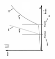
図2は、光通信システムで使用されるような典型的なレーザダイオードの特性を示す図である。レーザダイオードを流れる電流は、変調された光信号を生成するために使用されるとき、最小電流が該レーザについての閾値203を超えると共に、最大電流がデバイスの製造元の定格を下回るように変調される。レーザダイオードが低温であるとき、または電流レベルが比較的低いとき、単純な線形モデル201で十分である。しかしながら、レーザダイオードが昇温したとき、またはその特性が経年変化するにつれて、閾値電流は変化し(204)、電流と光出力の関係はより湾曲した形状202を示すことがある。したがって、システムの寿命に亘って動作中に所望の光出力および所望のERを維持することは簡単ではない。
FIG. 2 is a diagram showing the characteristics of a typical laser diode as used in an optical communication system. When used to generate a modulated optical signal, the current through the laser diode is modulated so that the minimum current exceeds the
所与の実際的なシステムでは、信頼性のある通信を確立するために必要な信号レベルに関して、レーザの平均動作パワーが規定のレベルに設定されるように最大電流を設定することができる。そのようなシステムにおける重要なパラメータは、通常は消光比(ER)と呼ばれる最大光出力と最小光出力の比であり、これは受信機の信号対雑音レベルに影響する。ERは、最小および最大のレーザダイオード電流値の関数であり、単純な線形関係として表されることもあるが、実際にはこれは正確な表現ではない。 In a given practical system, the maximum current can be set so that the average operating power of the laser is set to a specified level with respect to the signal level required to establish reliable communication. An important parameter in such a system is the ratio of maximum light output to minimum light output, commonly referred to as the signal-to-noise ratio (ER), which affects the signal-to-noise level of the receiver. ER is a function of the minimum and maximum laser diode current values, sometimes expressed as a simple linear relationship, but in practice this is not an exact representation.
図3は、高温でのレーザダイオードの平均光パワー301が、最小の光レベル302および最大の光レベル303、したがってERの正確な推定の基礎としてどのように適していないかを示している。これはまた、所望の平均パワーおよびERを得るために必要な最小304および最大305の電流レベルを制御することに問題があることを意味している。システムが連続的なデータストリームで動作する場合、レーザは定常状態の温度に達することができるので、平均値をモニタすることは比較的容易である。さらに、モニタダイオードシステムからデータを収集し、ピークおよびトラフの光データレベルを測定値の何等かの種類の平均化により測定して、ERおよび平均光パワーの推定値を提供するための時間がある。この目的のためのシステムは、先行技術において知られている(例えば、Smith et al, Electronics Letter Vol 14, 1978,および同様の派生的装置)。
FIG. 3 shows how the average
図4は、(標準的なITU-T勧告G.984.2のような)バーストモード動作の仕様に準拠したシステムにおけるデータバーストを送信することを目的とした光信号の一般的な形態を示している。レーザへのバイアス電流は、データ信号111がレーザ出力を変調するために使用される前に、バーストイネーブル信号112によってゲート制御される。そのような規格では、データバースト403の持続時間T1は正確に定義され、典型的には数100ナノ秒のオーダーである。データバーストの終わりに、論理値はハイ状態(論理ハイ値)またはロー状態(論理ロー値)であり得ることに留意されたい。そのような規格はまた、典型的にはT2をレーザ出力がゼロに戻らなければならない時間間隔404と定義する。実際のバイアス制御システムの帯域幅を考慮すると、この間隔は10ナノ秒のオーダーである。
FIG. 4 shows a general form of an optical signal intended to transmit a data burst in a system conforming to the specifications for burst mode operation (such as standard ITU-T Recommendation G.984.2). ing. The bias current to the laser is gate controlled by the burst enable
そのようなバーストモードシステムでは、平均パワーおよびERを制御する問題は困難である。バーストが始まる前、レーザは比較的冷たい状態にある。データパケットが送信されるとすぐに、レーザは昇温し始め、通常のバーストの間も昇温し続ける。システムの動作パラメータが制御されるような、例えば5回以下の短いトレーニングバースト後にシステムが動作可能であることが規格の要件である。 In such a burst mode system, the problem of controlling average power and ER is difficult. Before the burst begins, the laser is relatively cold. As soon as the data packet is transmitted, the laser begins to heat up and continues to heat up during the normal burst. It is a requirement of the standard that the system be operational after, for example, 5 or less short training bursts in which the operating parameters of the system are controlled.
一連のバーストの開始後迅速に動作条件を確立することができるという要件は、この開示では扱われていない。この問題を他の手段で解決するために残して、レーザが上昇した平均温度まで実質的に暖まったところで最初のトレーニングバーストの後にレーザ出力の消光比を正確に制御するための手段を提供する要求が依然としてある。ピーク値とトラフ値の測定には、連続システムの場合と同じモニタチャネル帯域幅の制限があるが、信号の断続的な性質によって要求がさらに複雑になり、意味のある平均化がより困難になる。 The requirement that operating conditions be established quickly after the start of a series of bursts is not addressed in this disclosure. A requirement to leave this problem to be solved by other means and to provide a means for precisely controlling the extinction ratio of the laser output after the first training burst where the laser has substantially warmed to the elevated average temperature. Is still there. Measuring peak and trough values has the same monitor channel bandwidth limitations as in continuous systems, but the intermittent nature of the signal makes the requirements more complex and makes meaningful averaging more difficult. ..
本発明の一実施形態では、データ「1」およびデータ「0」の値を表す光出力の瞬時値、または定義され得るような他の値の迅速かつ正確な推定を行うための手段が提供される。当該推定値を使用して、所望の出力レベルを供給するために必要なバイアス電流および変調電流の必要値を計算することができると共に、短期間の昇温および/または長期間の経年劣化によるレーザ特性の変化にかかわらずこれらを維持することができる更なる手段が提供される。 In one embodiment of the invention there is provided a means for making a rapid and accurate estimate of the instantaneous value of the optical output representing the values of data "1" and data "0", or other values as may be defined. To. The estimates can be used to calculate the required bias and modulation currents required to provide the desired output level, as well as lasers due to short-term warming and / or long-term aging. Further means are provided that can maintain these regardless of changes in properties.
図4において、データのバースト後にレーザをオフにする時間は一定ではなく、データ送信期間401の終了時の論理値に依存することに留意されたい。データ送信期間の終わりのハイ状態からのレーザバイアスターンオフ時間405は、データ伝送期間終わりのロー状態からのレーザバイアスターンオフ時間406よりも長い。変調データ信号111に応答する変調回路110の帯域幅は非常に速い。したがって、バイアス電流制御を使用して「ハイ」状態からオフにするのではなく、変調回路を使用して、最初にレーザ出力を非常に急速に、通常は数十ピコ秒程度の時間で「ロー」状態へ低減することができる。レーザ出力が上記「ロー」状態になると、完全な消光にターンオフする作業ははるかに容易になる。さらに、規格によって要求される間隔404より実質的に短い時間間隔で、バイアス電流114がバーストイネーブル信号112または実質的に同等の信号に応答することを確実にすることは困難な作業ではない。このアプローチは、それほど長くはないがそれでもなおそのようなモニタチャネル回路に典型的な過渡整定時間よりも長い時間間隔を利用可能にする。この知識を用いて、一般の光学的な「ハイ」および「ロー」出力レベルについての有用な測定を実行するために、指定されたターンオフ間隔404において利用可能な時間を活用することが可能である。
Note that in FIG. 4, the time to turn off the laser after a burst of data is not constant and depends on the logical value at the end of the
図5は、ハイレベルおよびローレベルの測定を容易にするために送信信号に巧妙な修正を加えたバーストモードシステムに関連する光レベルを示す。当該修正は、それらがバーストパケット内のデータの通常の伝送に影響を与えず、関連のある規格によって設定された仕様を超えないようになされる。 FIG. 5 shows the light levels associated with a burst mode system with subtle modifications to the transmitted signal to facilitate high and low level measurements. The modification is made so that they do not affect the normal transmission of data in burst packets and do not exceed the specifications set by the relevant standards.
上記修正のためのフレームワークを提供するために、規格によって許容されるレーザターンオフ時間405より実質的に短いものの、モニタチャネル出力105の整定時間より実質的に長くなるのに十分長いという条件を満たすように、時間間隔が最初に定義される。同時に、該時間間隔は、バイアス電流制御回路がレーザを完全に消光するために期間405内に十分な残り時間を与える。本発明の特徴は、生データ信号111を修正された形態のレーザ変調信号501で置き換えることであり、各バーストの終わりの既知の論理値が延長期間T3,502の間保持される。同時に、レーザへのバイアス電流114は、そのバーストのデータが終了した後、規定された期間バイアスがアクティブのままであるように、バーストイネーブル信号(バイアス制御信号506)の修正バージョンによって制御される。データバーストのこの延長部分の論理値は、図5の503で示される「1」と図5の504で示される「0」との間で交互に繰り返すようにされる。この論理値保持期間502の持続時間は、モニタチャネル出力105が実質的に正確な測定結果に落ち着くことができるのに十分な長さとされる。データバーストの終わりに保持された論理値が「1」である場合、レーザ変調電流115は、この延長期間502の終わりに、データ変調回路110へのコマンドエッジ505によって「0」に戻される。このようにして、レーザ電流は、遥かに遅いバイアス電流制御によってではなく、非常に短い時間(この例では数十ピコ秒)で広帯域幅回路機能によって、その消光状態に向かって実質的に減少される。この状態に達するとすぐに、バイアス電流114は、バイアス制御信号506によってオフにされると共に、関連する規格によって許容される時間の終了前にゼロまで減衰する。したがって、これら若しくは実質的に同様の手段によって、モニタ出力105は、先行技術においてしばしばそうであるように特定のデータパターンおよび/またはランレングスから生じる著しい制限なしに、論理「1」および論理「0」の両方のデータ状態の間に、適正で一般的な光出力の実質的に正確な表現を伝えることができる。交互のデータバーストから得られたこれらの測定値からアナログ値をデジタル形式113に変換することができ、簡単なアルゴリズムを用いて一般的な消光比および平均光パワーを決定するためのシステムを完成することができ、さらに、ERおよび平均パワーがシステムに対する所望の目標値と一致するように、変調電流およびバイアス電流に対する必要な調整を決定することができる。
To provide a framework for the above modifications, the condition is that the laser turn-off time is substantially shorter than the laser turn-
本発明の利点は、上記のように構成された制御システムが、該システムの他の部分の性能に関する重要な仮定から解放され、実質的に間接計算からは導出されない、論理「1」および論理「0」の両方に対する定常状態の光学的な値を測定するという点である。
本発明の更なる利点は、バーストモード信号の断続的な性質が制御システムの働きを減じることがない点である。
The advantage of the present invention is that the control system configured as described above is freed from important assumptions about the performance of other parts of the system and is not substantially derived from indirect computation, logic "1" and logic "1". The point is to measure steady-state optical values for both "0".
A further advantage of the present invention is that the intermittent nature of the burst mode signal does not diminish the function of the control system.
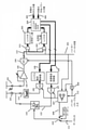
図6は、本発明の一実施形態による構成を示す。バイアス電流114は、電流出力デジタル-アナログ変換器(DAC)106によって設定され、変調電流115は、他のDAC107によって同様に設定される。それらのDACのための制御デジタル値はデジタル計算機能604によって決定され、該デジタル計算機能604は、その入力をシステムフィードバック値と所望の平均パワー606および変調深度(またはER605)に対応するデジタル入力とから取得する。変調回路110は、本実施形態ではデータ入力111によって直接制御されず、選択回路、例えばセレクタスイッチ機能610によって、データ入力111と論理「1」または論理「0」との間でその入力を切り替えることができる。データバーストの開始を示すためにバーストイネーブル信号112がアサートされると、論理制御機能607は、セレクタ610を使用して変調入力経路を設定し、入力データを変調回路110に直接渡す。変調された光信号がレーザ101によって生成され、モニタダイオード102とそれに関連する増幅器103とによって帯域制限されたモニタ信号105が生成される。このモニタ信号105は、アナログ-デジタル変換器(ADC)104によってデジタル値113に変換される。データバーストのペイロードの間、この出力113を使用することができるが、それはこのチャネルの帯域幅制限のために制限された値のものとなる。データペイロードの終わりに、バーストイネーブル信号はこの送信の終わりを示す。従来のシステムでは、これは変調電流115およびバイアス電流114を完全に無効にするであろう。
FIG. 6 shows a configuration according to an embodiment of the present invention. The bias current 114 is set by the current output digital-to-analog converter (DAC) 106, and the modulation current 115 is similarly set by the
本発明のこの実施形態によれば、制御ロジック607は、規定された遅延時間609を取り、バイアス電流および変調電流をオンに保持する。各データバーストと共に論理値を変更し、バーストを「ハイ」または「ロー」として効果的に指定する具体化によって、追加のバースト状態信号601が提供される。例示的な具体化として、バーストが「ハイ」として指定されている場合、バーストの終わりの遅延中に、変調入力セレクタ610は、光出力がハイレベルに保持されるように論理「1」503に設定される。この変調光学値は、その限定された帯域幅にもかかわらずモニタチャネルが正確な測定を行うのに十分に長い期間502の間保持されるが、それでもレーザを完全に消光する時間として十分に短い。モニタチャネル出力105はデジタル形式113に変換され、次にバースト状態信号601によってイネーブルされた論理ゲート611を介して適切な時点で第1のレジスタ602に渡される。そして、このレジスタは、測定された光学的な「ハイ」の値を計算機能604に与える。
According to this embodiment of the invention, the
この延長期間502の終わりに、変調セレクタは、通常の変調回路を使用してレーザ変調電流115を除去するために論理「0」に設定され、それゆえに、光出力を非常に急速に減少させる。同じ瞬間505において、制御ロジック607は、バイアス電流DAC106および変調電流DAC107に出力電流を停止するように命令し、その結果、レーザ101は、関連する通信規格によって要求される期間404内に完全に消光する。
At the end of this
バースト状態信号601によってバーストが「ロー」として指定されている場合、データペイロードの終わりに、変調セレクタ610は論理「0」(図5の504)に設定され、レーザ出力はローレベル302になる。バーストデータペイロードの最後のシンボルがバーストの終わりに論理「1」を必要としたとしても、通常の変調回路110を使用することによって論理「0」への遷移を非常に高速に行うことができる。やはり、この変調光学値は、モニタチャネルがその限られた帯域幅にもかかわらず正確な測定を行うのに十分長い期間502の間保持されるが、それでもレーザを完全に消光する時間として十分に短い。
If the burst is designated as "low" by the
次に、モニタチャネル出力105は、デジタル形式113に変換された後、バースト状態信号601の論理補数によってイネーブルにされた論理ゲート612を介して第2のレジスタ603に適切な時点で渡される。そして、このレジスタは、測定された光学的な「ロー」の値を計算機能604に与える。
The
便利で効率的な配置は、バーストを交互に「ハイ」および「ロー」に指定することであろう。しかし、本発明はまた、あるレベルの推定値を他のレベルよりも早く取得する必要がある場合、または、システムの他の要件を考慮に入れる必要がある場合に、他の何等かの「ハイ」および「ロー」状態のシーケンスを使用してもよい。 A convenient and efficient placement would be to specify bursts alternately as "high" and "low". However, the invention also has some other "high" when it is necessary to obtain an estimate of one level faster than another, or when other requirements of the system need to be taken into account. And "low" state sequences may be used.
次に、計算機能604は、平均値606およびER605に必要な目標値入力を取得し、簡単な計算を使用して、該計算されたER値と平均値との間の誤差が最小になるように新しいバイアス電流制御値108および新しい変調電流値109を導出し、そして、対応する要求されたERおよび平均値の誤差が最小化され、無視できるレベルまたは許容レベルになる。このプロセスは、「ハイ」および「ロー」バーストを数回繰り返すことがあり、システムの正確な収束速度は、特定のアプリケーション用に選択された係数および倍率に依存する。
The
図7は、本発明の別の実施形態による構成を示している。この構成では、バイアス電流および変調電流に対する補正の導出は、よりアナログ的な処理で実行される。レーザ変調およびモニタ回路は、図6による前述した構成と実質的に同じである。モニタチャネル105の出力をデジタル形式に変換する代わりに、当該アナログ値は、DACによってユーザ定義入力値から生成された基準アナログ値より導出された別のアナログ値と直接比較される。その動作は以下の通りである。
FIG. 7 shows a configuration according to another embodiment of the present invention. In this configuration, the derivation of corrections for bias and modulation currents is performed in a more analog way. The laser modulation and monitor circuit is substantially the same as the configuration described above with reference to FIG. Instead of converting the output of
所望の光学的「ハイ」値701、および所望の光学的「ロー」値702は、明示的な形でユーザから与えられ、2つのDAC703およびDAC704をそれぞれ制御するために使用される。これらのDACの出力705および出力706は、理想的な光バイアス条件および所望の変調値の下での光学的「1」および光学的「0」に対する、所望のモニタフォトダイオードおよび増幅器の出力105と等価である。また、当業者は、所望の動作電流が平均値およびER値としても供給され、そして、単純な演算回路によって同等の「ハイ」値および「ロー」値に変換され得ることを直ちに認識するであろう。
The desired optical "high"
理想的な条件下でレーザが論理「ハイ」の状態で動作しているとき、電圧105および電圧705は実質的に同一であるべきである。理想的な条件下でレーザが論理「ロー」の状態で動作しているとき、電圧105と電圧706は実質的に同一であるべきである。比較器707および比較器708は、モニタ表示されたレベルと所望のレベルとの間のあらゆる差の符号を決定するために使用される。
When the laser is operating in the logical "high" state under ideal conditions, the
データバーストが「ハイ」と指定されている場合、延長期間502の終わりに、比較器707の出力は、バースト状態信号601によって制御される論理ゲート611を介してカウンタ712に渡され、比較器707の出力の符号に応じてカウントプロセスをアップまたはダウンのどちらかに制御するために使用される。この時にモニタ信号105がDAC703からの基準信号705よりも小さい場合、カウンタは減少し、「ハイ」の光学的状態に対する負の誤差を示す。モニタ信号105が基準信号705より大きい場合には、カウンタ712は増加する。
If the data burst is designated as "high", at the end of the
同様に、データバーストが「ロー」と指定されている場合、延長期間502の終わりに、比較器708の出力は、バースト状態信号601の補数によって制御される論理ゲート612を介してカウンタ713に渡され、比較器708の出力の符号に応じて同様のカウントプロセスをアップまたはダウンのどちらかに制御するために使用される。この時にモニタ信号105がDAC704からの基準信号706より小さい場合、カウンタは減少し、「ロー」の光学的状態に対する負の誤差を示す。この時にモニタ出力がレプリカより高い場合には、対応する増分が行われる。
Similarly, if the data burst is designated as "low", at the end of the
論理演算ブロック604は、任意の時点におけるカウンタ712およびカウンタ713からの値より、モニタ出力105とレプリカ経路710との間で監視された誤差を補正するのに必要なバイアス制御値108および変調値109を容易に計算することができる。多数のデータバーストに亘って、システムは、誤差が最小になるように電流を調整し、よって、レーザは、実質的に所望の平均光出力および実質的に所望のERで動作することになる。
The
本発明を特定の実施例およびその可能な実施形態を参照して説明してきたが、これらは決して本発明の範囲を限定するものとして解釈されるべきではない。特許請求の範囲に記載されている本発明の範囲から逸脱することなく、他の多くの可能な実施形態、変更および改良を本発明に組み込むことができ、または本発明と共に組み込むことができることは明らかである。 Although the present invention has been described with reference to specific examples and possible embodiments thereof, they should by no means be construed as limiting the scope of the invention. It is clear that many other possible embodiments, modifications and improvements can be incorporated into, or combined with, the invention without departing from the scope of the invention as described in the claims. Is.
Claims (21)
規定のバースト期間中のデータ送信期間の間にデータ入力値を選択すると共に、前記規定のバースト期間中かつ前記データ送信期間の直後の延長期間の間に論理ハイ値および論理ロー値の一方を選択して、少なくとも2つのバーストの前記シーケンスについて、少なくとも1つのバーストは論理ロー値の延長期間を有し、少なくとも1つのバーストは論理ハイ値の延長期間を有するように、データ入力値、論理ハイ値または論理ロー値のうちの1つを選択するように構成された選択回路と、
前記規定のバースト期間中に前記選択回路によって選択された値またはゼロ値に対応する電流であって、レーザダイオードが光出力を供給するような前記電流をレーザダイオードに与えるように構成された駆動回路と、
前記レーザダイオードの光出力に対応するセンサモジュール出力であって、少なくとも2つのバーストの前記シーケンスにおける前記論理ハイ値および前記論理ロー値に対応した前記レーザダイオードの光出力に比例する電気出力を与える前記センサモジュール出力を提供するように構成された光センサモジュールと、
前記レーザダイオードの所望の最小および最大光出力パワーレベルに関する値を受信すると共に、前記論理ハイ値および前記論理ロー値に対応した光出力パワーレベルに比例する電気出力を前記光センサモジュールから受信し、当該受信情報を使用して前記駆動回路に制御値を提供するように構成されたコントローラと、
を含むシステム。 A system for transmitting a sequence of at least two data bursts in a fiber optic communication system.
Select the data input value during the data transmission period during the specified burst period, and select either the logical high value or the logical low value during the specified burst period and during the extension period immediately after the data transmission period. Then, for the sequence of at least two bursts, the data input value, the logical high value, such that at least one burst has a logical low value extension period and at least one burst has a logical high value extension period. Or a selection circuit configured to select one of the logical row values,
A drive circuit configured to provide the laser diode with the current corresponding to the value selected by the selection circuit or the zero value during the specified burst period, such that the laser diode supplies the light output. When,
The sensor module output corresponding to the optical output of the laser diode, which provides an electrical output proportional to the optical output of the laser diode corresponding to the logical high value and the logical low value in the sequence of at least two bursts. With an optical sensor module configured to provide sensor module output,
The optical sensor module receives values for the desired minimum and maximum optical output power levels of the laser diode and also receives electrical outputs proportional to the optical output power levels corresponding to the logical high and logical low values. A controller configured to use the received information to provide control values to the drive circuit.
System including.
規定のバースト期間中のデータ送信期間の間にデータ入力値が選択されると共に、前記規定のバースト期間中かつ前記データ送信期間の直後の延長期間の間に論理ハイ値および論理ロー値の一方が選択されて、少なくとも2つのバーストの前記シーケンスについて、少なくとも1つのバーストは論理ロー値の延長期間を有し、少なくとも1つのバーストは論理ハイ値の延長期間を有するように、データ入力値、論理ハイ値または論理ロー値のうちの1つを選択することと、
前記規定のバースト期間中に選択された値またはゼロ値に対応する電流であって、レーザダイオードが光出力を供給するような前記電流をレーザダイオードに与えることと、
前記光出力に対応するセンサモジュール出力を用いることによって、少なくとも2つのバーストの前記シーケンスにおける前記論理ハイ値および前記論理ロー値に対応したレーザダイオードの光出力に比例する電気出力を決定することと、
前記レーザダイオードの所望の最小および最大光出力パワーレベルに関する値を受信することと、
前記論理ハイ値および前記論理ロー値に対応した光出力に比例する前記電気出力と、前記レーザダイオードの所望の最小および最大光出力パワーレベルに関する前記受信された値とに基づいて、前記レーザダイオードに与えられる前記電流についての制御値を提供することと、
を含む方法。 A method for transmitting a sequence of at least two data bursts in a fiber optic communication system.
The data input value is selected during the data transmission period during the specified burst period, and one of the logical high value and the logical low value is selected during the specified burst period and during the extension period immediately after the data transmission period. For the sequence of at least two bursts selected, the data entry value, logical high such that at least one burst has a logical low value extension period and at least one burst has a logical high value extension period. Choosing one of the values or logical row values,
To give the laser diode the current corresponding to the selected or zero value during the specified burst period, such that the laser diode supplies the light output.
By using the sensor module output corresponding to the optical output, determining the electrical output proportional to the optical output of the laser diode corresponding to the logical high value and the logical low value in the sequence of at least two bursts.
Receiving values for the desired minimum and maximum light output power levels of the laser diode
The laser diode is based on the electrical output proportional to the optical output corresponding to the logical high and low values and the received values for the desired minimum and maximum optical output power levels of the laser diode. To provide a control value for the given current and
How to include.
Applications Claiming Priority (3)
| Application Number | Priority Date | Filing Date | Title |
|---|---|---|---|
| GB1611938.0 | 2016-07-08 | ||
| GB1611938.0A GB2541291B (en) | 2016-07-08 | 2016-07-08 | Laser power controller |
| PCT/EP2017/067090 WO2018007587A1 (en) | 2016-07-08 | 2017-07-07 | Laser power controller |
Publications (3)
| Publication Number | Publication Date |
|---|---|
| JP2019525684A JP2019525684A (en) | 2019-09-05 |
| JP2019525684A5 JP2019525684A5 (en) | 2020-05-14 |
| JP6992062B2 true JP6992062B2 (en) | 2022-01-13 |
Family
ID=56890880
Family Applications (1)
| Application Number | Title | Priority Date | Filing Date |
|---|---|---|---|
| JP2019521182A Active JP6992062B2 (en) | 2016-07-08 | 2017-07-07 | Laser power controller |
Country Status (5)
| Country | Link |
|---|---|
| US (1) | US10205532B2 (en) |
| JP (1) | JP6992062B2 (en) |
| CN (1) | CN109565150B (en) |
| GB (1) | GB2541291B (en) |
| WO (1) | WO2018007587A1 (en) |
Families Citing this family (5)
| Publication number | Priority date | Publication date | Assignee | Title |
|---|---|---|---|---|
| US10749605B2 (en) * | 2016-07-08 | 2020-08-18 | Hilight Semiconductor Limited | Laser power controller |
| GB2562138B (en) * | 2018-01-12 | 2019-06-12 | Hilight Semiconductor Ltd | Laser power controller |
| CN110945802B (en) | 2017-07-29 | 2023-01-20 | 光速株式会社 | Optical transmitter operating in burst mode and method for controlling optical transmitter operating in burst mode |
| CN108781116B (en) * | 2017-11-30 | 2022-04-22 | 深圳市大疆创新科技有限公司 | Power adjustment method and laser measurement device |
| CN115733044B (en) * | 2022-11-30 | 2024-01-30 | 江苏亮点光电研究有限公司 | TGC index function laser beacon circuit |
Citations (5)
| Publication number | Priority date | Publication date | Assignee | Title |
|---|---|---|---|---|
| JP2002319897A (en) | 2001-04-19 | 2002-10-31 | Fujikura Ltd | Optical burst transmission method and laser diode driving circuit therefor |
| JP2005123350A (en) | 2003-10-16 | 2005-05-12 | Matsushita Electric Ind Co Ltd | Average power detecting circuit, laser diode driving circuit and light transmitting module |
| US20100254717A1 (en) | 2009-04-06 | 2010-10-07 | Avago Technologies Fiber Ip (Singapore) Pte. Ltd. | Apparatus and method for controlling the optical output power of a laser in an optical transmitter (tx) |
| CN102624458A (en) | 2012-03-12 | 2012-08-01 | 东南大学 | Output power control method of burst mode laser driver |
| WO2014038338A1 (en) | 2012-09-06 | 2014-03-13 | 住友電気工業株式会社 | Optical communications module, home-side device, and control method for light-emitting element |
Family Cites Families (29)
| Publication number | Priority date | Publication date | Assignee | Title |
|---|---|---|---|---|
| GB1539624A (en) * | 1976-02-11 | 1979-01-31 | Standard Telephones Cables Ltd | Laser control system |
| CA1210070A (en) * | 1984-10-26 | 1986-08-19 | Northern Telecom Limited | Laser transmitter |
| US4709416A (en) * | 1986-02-24 | 1987-11-24 | Rca Corporation | Laser bias current stabilization for burst mode fiber optic communication system |
| WO1993013577A1 (en) * | 1991-12-20 | 1993-07-08 | Raynet Corporation | Apparatus and method for controlling an extinction ratio of a laser diode over temperature |
| US5502298A (en) * | 1992-12-21 | 1996-03-26 | Ericsson Raynet | Apparatus and method for controlling an extinction ratio of a laser diode over temperature |
| JP2631080B2 (en) * | 1993-10-05 | 1997-07-16 | 株式会社小松製作所 | Output control device of laser device |
| JP2531117B2 (en) * | 1993-12-01 | 1996-09-04 | 日本電気株式会社 | High-speed APC circuit |
| US5850409A (en) * | 1997-03-21 | 1998-12-15 | Maxim Integrated Products, Inc. | Laser modulation control method and apparatus |
| US6167246A (en) * | 1997-05-09 | 2000-12-26 | Micrel Incorporated | Fully integrated all-CMOS AM receiver |
| JP3840794B2 (en) * | 1998-04-13 | 2006-11-01 | 富士ゼロックス株式会社 | Laser drive device |
| US6219165B1 (en) * | 1998-07-09 | 2001-04-17 | Agere Systems Optoelectronics Guardian Corp. | Burst-mode laser techniques |
| US6917639B2 (en) * | 2001-08-09 | 2005-07-12 | Ricoh Company, Ltd. | Laser driver circuit |
| US6778569B2 (en) * | 2001-11-15 | 2004-08-17 | Agere Systems Inc. | Optical source driver with improved input stage |
| US7505498B2 (en) * | 2002-01-08 | 2009-03-17 | Jorge Sanchez | Apparatus and method for measurement for dynamic laser signals |
| JP4043844B2 (en) * | 2002-05-24 | 2008-02-06 | フリースケール セミコンダクター インコーポレイテッド | Light emitting element driving device |
| JP2004172237A (en) * | 2002-11-18 | 2004-06-17 | Sharp Corp | Optical transmission control unit |
| US7443896B2 (en) * | 2003-07-09 | 2008-10-28 | Agere Systems, Inc. | Optical midpoint power control and extinction ratio control of a semiconductor laser |
| US7265334B2 (en) * | 2004-11-19 | 2007-09-04 | Mindspeed Technologies, Inc. | Laser power control with automatic compensation |
| US7792166B2 (en) | 2005-06-24 | 2010-09-07 | Lockheed Martin Corporation | Apparatus and method for driving laser diodes |
| US7853154B2 (en) * | 2006-01-13 | 2010-12-14 | Mindspeed Technologies, Inc. | Bias circuit for burst-mode/TDM systems with power save feature |
| US7724792B2 (en) * | 2006-03-03 | 2010-05-25 | Mindspeed Technologies, Inc. | Driving laser diodes with immunity to temperature changes, aging, and other effects |
| US8094692B2 (en) * | 2008-02-22 | 2012-01-10 | Nippon Telegraph And Telephone Corporation | Modulation method, modulation program, recording medium, modulation device, and optical transmitter |
| US9479255B2 (en) * | 2008-04-30 | 2016-10-25 | Arris Enterprises, Inc. | Method and apparatus for controlling the optical output power from a burst mode laser |
| CN101692521B (en) * | 2009-10-16 | 2012-04-18 | 上海博为光电科技有限公司 | Laser diode driver for optical communication transmitter |
| CN102237633A (en) * | 2010-04-23 | 2011-11-09 | 上海华魏光纤传感技术有限公司 | High-power narrow-pulse laser light source |
| TWI426821B (en) * | 2010-08-27 | 2014-02-11 | Tm Technology Inc | Automatic power control (apc) loop for controlling bias current of laser diode |
| US8576888B2 (en) | 2010-10-29 | 2013-11-05 | Maxim Integrated Products, Inc. | Dual laser-power-level control and calibration system for burst-mode and continuous-mode transmitter |
| US8971364B2 (en) * | 2011-01-19 | 2015-03-03 | Coherent, Inc. | Driving circuit for analog-modulated diode-laser |
| JP6032075B2 (en) * | 2013-03-18 | 2016-11-24 | 富士通株式会社 | Optical transmission device and optical transmission system |
-
2016
- 2016-07-08 GB GB1611938.0A patent/GB2541291B/en active Active
-
2017
- 2017-07-07 CN CN201780042380.7A patent/CN109565150B/en active Active
- 2017-07-07 US US15/643,958 patent/US10205532B2/en active Active
- 2017-07-07 JP JP2019521182A patent/JP6992062B2/en active Active
- 2017-07-07 WO PCT/EP2017/067090 patent/WO2018007587A1/en active Application Filing
Patent Citations (5)
| Publication number | Priority date | Publication date | Assignee | Title |
|---|---|---|---|---|
| JP2002319897A (en) | 2001-04-19 | 2002-10-31 | Fujikura Ltd | Optical burst transmission method and laser diode driving circuit therefor |
| JP2005123350A (en) | 2003-10-16 | 2005-05-12 | Matsushita Electric Ind Co Ltd | Average power detecting circuit, laser diode driving circuit and light transmitting module |
| US20100254717A1 (en) | 2009-04-06 | 2010-10-07 | Avago Technologies Fiber Ip (Singapore) Pte. Ltd. | Apparatus and method for controlling the optical output power of a laser in an optical transmitter (tx) |
| CN102624458A (en) | 2012-03-12 | 2012-08-01 | 东南大学 | Output power control method of burst mode laser driver |
| WO2014038338A1 (en) | 2012-09-06 | 2014-03-13 | 住友電気工業株式会社 | Optical communications module, home-side device, and control method for light-emitting element |
Also Published As
| Publication number | Publication date |
|---|---|
| GB201611938D0 (en) | 2016-08-24 |
| WO2018007587A1 (en) | 2018-01-11 |
| JP2019525684A (en) | 2019-09-05 |
| GB2541291B (en) | 2018-06-20 |
| CN109565150A (en) | 2019-04-02 |
| GB2541291A (en) | 2017-02-15 |
| US20180019823A1 (en) | 2018-01-18 |
| US10205532B2 (en) | 2019-02-12 |
| CN109565150B (en) | 2020-11-06 |
Similar Documents
| Publication | Publication Date | Title |
|---|---|---|
| JP6992062B2 (en) | Laser power controller | |
| WO2018119637A1 (en) | Method and device for controlling wavelength of light emitting assembly | |
| US10727950B2 (en) | Method of controlling optical transmitter operable for pulse-amplitude modulation signal | |
| JP3748432B2 (en) | LIGHT EMITTING DEVICE CONTROL DEVICE, OPTICAL TRANSMITTER, DRIVE CURRENT DETERMINING METHOD, AND PROGRAM | |
| JP5134104B2 (en) | Method and apparatus for compensating for optical crosstalk in optical output power feedback monitoring system of parallel optical transmitter | |
| US20050008280A1 (en) | Extinction ratio control of a semiconductor laser | |
| JP2011010286A (en) | Apparatus and method for adaptively controlling impulse response of optical signal output from laser of optical transmitter (tx) | |
| US10447007B2 (en) | Method and system for controlling laser modulation | |
| KR100670829B1 (en) | Apparatus and method for maintaing constant extinction ratio of laser diode | |
| CN110034487B (en) | Laser power controller | |
| US9154227B2 (en) | Port monitoring device and port monitoring method | |
| US10749605B2 (en) | Laser power controller | |
| EP1594238A2 (en) | Method and system for controlling laser diodes in optical communications systems | |
| US8301035B2 (en) | Optical communication apparatus, control apparatus, and method for controlling optical output | |
| GB2552726B (en) | Method for control of optical intensity and extinction ratio of laser modulation in an optical transmitter | |
| US20220352987A1 (en) | Optical transmitter device, optical transmission device, and optimum-phase-amount calculation method | |
| JP2015130500A (en) | Method of improving stability of light source in optical network testing apparatus, and computer program product | |
| US20220303019A1 (en) | Adjustment device and adjusting method for stabilizing optical characteristic parameters | |
| GB2552725B (en) | Method for control of optical intensity and extinction ratio of laser modulation in an optical transmitter | |
| CN103840364A (en) | Wavelength control method and device of tunable laser | |
| US10535978B2 (en) | Method for control of optical intensity and extinction ratio of laser modulation in an optical transmitter | |
| US11646540B2 (en) | Variable optical attenuator assisted control of optical devices | |
| KR101692897B1 (en) | Laser diode characteristic estimation apparatus for optical communication and control section selecting system | |
| US20190356292A1 (en) | Variable step size to reduce convergence time of a control loop | |
| TW201448389A (en) | A method and an optical transmitter suppressing wavelength deviation at the beginning of operation |
Legal Events
| Date | Code | Title | Description |
|---|---|---|---|
| A521 | Written amendment |
Free format text: JAPANESE INTERMEDIATE CODE: A523 Effective date: 20190318 |
|
| A521 | Written amendment |
Free format text: JAPANESE INTERMEDIATE CODE: A523 Effective date: 20200401 |
|
| A621 | Written request for application examination |
Free format text: JAPANESE INTERMEDIATE CODE: A621 Effective date: 20200401 |
|
| A977 | Report on retrieval |
Free format text: JAPANESE INTERMEDIATE CODE: A971007 Effective date: 20210212 |
|
| A131 | Notification of reasons for refusal |
Free format text: JAPANESE INTERMEDIATE CODE: A131 Effective date: 20210316 |
|
| TRDD | Decision of grant or rejection written | ||
| A01 | Written decision to grant a patent or to grant a registration (utility model) |
Free format text: JAPANESE INTERMEDIATE CODE: A01 Effective date: 20211119 |
|
| A61 | First payment of annual fees (during grant procedure) |
Free format text: JAPANESE INTERMEDIATE CODE: A61 Effective date: 20211208 |
|
| R150 | Certificate of patent or registration of utility model |
Ref document number: 6992062 Country of ref document: JP Free format text: JAPANESE INTERMEDIATE CODE: R150 |