JP6991873B2 - Display device and inspection method - Google Patents
Display device and inspection method Download PDFInfo
- Publication number
- JP6991873B2 JP6991873B2 JP2018015648A JP2018015648A JP6991873B2 JP 6991873 B2 JP6991873 B2 JP 6991873B2 JP 2018015648 A JP2018015648 A JP 2018015648A JP 2018015648 A JP2018015648 A JP 2018015648A JP 6991873 B2 JP6991873 B2 JP 6991873B2
- Authority
- JP
- Japan
- Prior art keywords
- circuit
- short
- connection terminals
- driver
- voltage
- Prior art date
- Legal status (The legal status is an assumption and is not a legal conclusion. Google has not performed a legal analysis and makes no representation as to the accuracy of the status listed.)
- Active
Links
Images


Landscapes
- Devices For Indicating Variable Information By Combining Individual Elements (AREA)
- Control Of Indicators Other Than Cathode Ray Tubes (AREA)
- Testing Of Short-Circuits, Discontinuities, Leakage, Or Incorrect Line Connections (AREA)
- Testing Electric Properties And Detecting Electric Faults (AREA)
Description
本発明は、表示装置及び検査方法に関する。 The present invention relates to a display device and an inspection method.
近年、液晶表示パネルや有機エレクトロルミネッセンス発光を用いた有機ELディスプレイパネル(OLED:Organic Electro-Luminescence Display)を用いた表示装置において、画素の高密度化(高精細化)が求められている。このような表示装置の高精細化に伴い、映像信号線や走査線の数も増加し、これら映像信号線や走査線を駆動するドライバICのピン数も増加している。例えば、LCDドライバを試験する半導体試験装置において、LCDドライバが仕様を満たしているかどうかの各種項目の試験を行う前に、コンタクト試験やピン間ショート試験を行う際の高速化技術が開示されている(例えば、特許文献1)。 In recent years, in a display device using a liquid crystal display panel or an organic EL display panel (OLED: Organic Electro-Luminescence Display) using organic electroluminescence light emission, high density (high definition) of pixels is required. With the increase in definition of such display devices, the number of video signal lines and scanning lines has also increased, and the number of pins of the driver IC for driving these video signal lines and scanning lines has also increased. For example, in a semiconductor test device for testing an LCD driver, a high-speed technique for performing a contact test or a pin-to-pin short-circuit test before testing various items to see if the LCD driver meets the specifications is disclosed. (For example, Patent Document 1).
スマートフォンのような携帯端末装置においては、高精細化と共に狭額縁化が可能な表示パネルが求められている。これに伴い、フレキシブル基板上にドライバICをCOF(Chip On Film)によって実装されるケースが増加している。ドライバICが実装されたフレキシブル基板は、表示パネルを構成するガラス基板にFOG(Film On Glass)によって実装される。 In mobile terminal devices such as smartphones, there is a demand for a display panel capable of narrowing the frame as well as high definition. Along with this, the number of cases where the driver IC is mounted on the flexible substrate by COF (Chip On Film) is increasing. The flexible substrate on which the driver IC is mounted is mounted on the glass substrate constituting the display panel by FOG (Film On Glass).
表示装置の高精細化に伴い、ドライバICが実装されたフレキシブル基板と表示パネルを構成するガラス基板との間の配線が多くなり、双方の基板の配線を接続する接続端子の間隔が狭くなってきている。接続端子の間隔が狭くなると、ガラス基板とフレキシブル基板との間に噛み込んだ導電性の異物によって、隣り合う接続端子間で短絡が発生する可能性が高くなる。また、導電性の異物の抵抗値によっては、表示検査において異常を視認できず、表示装置の出荷品質が低下する可能性がある。 As the definition of the display device becomes higher, the wiring between the flexible board on which the driver IC is mounted and the glass board constituting the display panel increases, and the distance between the connection terminals connecting the wiring of both boards becomes narrower. ing. When the distance between the connection terminals is narrowed, there is a high possibility that a short circuit will occur between the adjacent connection terminals due to the conductive foreign matter caught between the glass substrate and the flexible substrate. Further, depending on the resistance value of the conductive foreign matter, the abnormality cannot be visually recognized in the display inspection, and the shipping quality of the display device may deteriorate.
本発明は、品質を向上することができる表示装置を提供することを目的とする。 An object of the present invention is to provide a display device capable of improving quality.
本発明の一態様に係る表示装置は、複数の画素が第1方向及び前記第1方向とは異なる第2方向に並ぶ表示部が設けられた第1基板と、前記表示部を駆動する駆動回路が集積されたドライバICと、前記ドライバICが設けられた第2基板と、前記表示部と前記ドライバICとの間に設けられ、前記第1基板に配置された信号選択回路と、前記第1基板に配線され、一端が前記信号選択回路に電気的に接続される複数の第1配線と、前記第2基板に配線され、一端が前記ドライバICに電気的に接続される複数の第2配線と、前記第1配線の他端と前記第2配線の他端とが電気的に接続された複数の接続端子と、を有し、前記ドライバICが取り得る制御状態として、前記信号選択回路が開制御され、隣り合う前記接続端子間に電位差が印加されない第1制御状態と、前記信号選択回路が開制御され、隣り合う前記接続端子間に電位差が印加される第2制御状態と、を含む。 The display device according to one aspect of the present invention includes a first substrate provided with a display unit in which a plurality of pixels are arranged in a first direction and a second direction different from the first direction, and a drive circuit for driving the display unit. A signal selection circuit provided between the display unit and the driver IC, a signal selection circuit provided between the driver IC, a second board provided with the driver IC, and the first board. A plurality of first wirings that are wired to the board and one end of which is electrically connected to the signal selection circuit, and a plurality of second wirings that are wired to the second board and one end of which is electrically connected to the driver IC. And a plurality of connection terminals in which the other end of the first wiring and the other end of the second wiring are electrically connected, and the signal selection circuit is a control state that the driver IC can take. It includes a first control state in which open control is performed and a potential difference is not applied between the adjacent connection terminals, and a second control state in which the signal selection circuit is open-controlled and a potential difference is applied between the adjacent connection terminals. ..
本発明の一態様に係る表示装置の検査方法は、複数の画素が第1方向及び前記第1方向とは異なる第2方向に並ぶ表示部が設けられた第1基板と、前記表示部を駆動する駆動回路が集積されたドライバICと、前記ドライバICが設けられた第2基板と、前記表示部と前記ドライバICとの間に設けられ、前記第1基板に配置された信号選択回路と、前記第1基板に配線され、一端が前記信号選択回路に電気的に接続される複数の第1配線と、前記第2基板に配線され、一端が前記ドライバICに電気的に接続される複数の第2配線と、前記第1配線の他端と前記第2配線の他端とが電気的に接続された複数の接続端子と、を有する表示装置の検査方法において、前記接続端子と前記表示部との間を遮断する第1ステップと、隣り合う前記接続端子間に電位差が印加されていない状態で、前記ドライバICに流れる第1電流値を取得する第2ステップと、隣り合う前記接続端子間に電位差が印加されている状態で、前記ドライバICに流れる第2電流値を取得する第3ステップと、前記第1電流値と前記第2電流値との差分を所定の電流閾値と比較する第4ステップと、前記差分が前記電流閾値よりも大きい場合に、隣り合う前記接続端子間において短絡が発生しているものとして判定する第5ステップと、を有する。 The inspection method of the display device according to one aspect of the present invention drives a first substrate provided with a display unit in which a plurality of pixels are arranged in a first direction and a second direction different from the first direction, and the display unit. A driver IC in which a driving circuit is integrated, a second board provided with the driver IC, a signal selection circuit provided between the display unit and the driver IC, and arranged on the first board. A plurality of first wires that are wired to the first board and one end of which is electrically connected to the signal selection circuit, and a plurality of first wires that are wired to the second board and one end of which is electrically connected to the driver IC. In an inspection method for a display device having a second wiring and a plurality of connection terminals in which the other end of the first wiring and the other end of the second wiring are electrically connected, the connection terminal and the display unit. The first step of cutting off between the two, the second step of acquiring the first current value flowing through the driver IC in a state where no potential difference is applied between the adjacent connection terminals, and the adjacent connection terminals. The third step of acquiring the second current value flowing through the driver IC while the potential difference is applied to the driver IC, and the third step of comparing the difference between the first current value and the second current value with a predetermined current threshold value. It has 4 steps and a 5th step in which it is determined that a short circuit has occurred between the adjacent connection terminals when the difference is larger than the current threshold value.
本発明の一態様に係る表示装置の検査方法は、複数の画素が第1方向及び前記第1方向とは異なる第2方向に並ぶ表示部が設けられた第1基板と、前記表示部を駆動する駆動回路が集積されたドライバICと、前記ドライバICが設けられた第2基板と、前記表示部と前記ドライバICとの間に設けられ、前記第1基板に配置される信号選択回路と、前記第1基板に配線され、一端が前記信号選択回路に電気的に接続される複数の第1配線と、前記第2基板に配線され、一端が前記ドライバICに電気的に接続された複数の第2配線と、前記第1配線の他端と前記第2配線の他端とが電気的に接続された複数の接続端子と、を有する表示装置の検査方法において、前記接続端子と前記表示部との間を遮断する第1ステップと、前記駆動回路から隣り合う前記接続端子に異なる電圧を供給する第2ステップと、隣り合う前記接続端子の一方の第1電圧値と、隣り合う前記接続端子の他方の第2電圧値とを検出する第3ステップと、前記第1電圧値と前記第2電圧値との差分を所定の電圧閾値と比較する第4ステップと、前記差分が前記電圧閾値よりも大きい場合に、隣り合う前記接続端子間において短絡が発生しているものとして判定する第5ステップと、を有する。 The inspection method of the display device according to one aspect of the present invention drives a first substrate provided with a display unit in which a plurality of pixels are arranged in a first direction and a second direction different from the first direction, and the display unit. A driver IC in which a driving circuit is integrated, a second board provided with the driver IC, a signal selection circuit provided between the display unit and the driver IC, and arranged on the first board. A plurality of first wires wired to the first board and one end electrically connected to the signal selection circuit, and a plurality of first wires wired to the second board and one end electrically connected to the driver IC. In an inspection method for a display device having a second wiring, a plurality of connection terminals to which the other end of the first wiring and the other end of the second wiring are electrically connected, the connection terminal and the display unit. The first step of cutting off between the two, the second step of supplying different voltages from the drive circuit to the adjacent connection terminals, the first voltage value of one of the adjacent connection terminals, and the adjacent connection terminals. The third step of detecting the other second voltage value, the fourth step of comparing the difference between the first voltage value and the second voltage value with a predetermined voltage threshold, and the difference from the voltage threshold. It also has a fifth step of determining that a short circuit has occurred between the adjacent connection terminals when the voltage is large.
以下に、本発明の実施形態について、図面を参照しつつ説明する。なお、開示はあくまで一例にすぎず、当業者において、発明の主旨を保っての適宜変更について容易に想到し得るものについては、当然に本発明の範囲に含有されるものである。また、図面は説明をより明確にするため、実際の態様に比べ、各部の幅、厚さ、形状等について模式的に表される場合があるが、あくまで一例であって、本発明の解釈を限定するものではない。また、本明細書と各図において、既出の図に関して前述したものと同様の要素には、同一の符号を付して、詳細な説明を適宜省略することがある。 Hereinafter, embodiments of the present invention will be described with reference to the drawings. It should be noted that the disclosure is merely an example, and those skilled in the art can easily conceive of appropriate changes while maintaining the gist of the invention, which are naturally included in the scope of the present invention. Further, in order to clarify the explanation, the drawings may schematically represent the width, thickness, shape, etc. of each part as compared with the actual embodiment, but this is just an example, and the interpretation of the present invention is used. It is not limited. Further, in the present specification and each figure, the same elements as those described above with respect to the above-mentioned figures may be designated by the same reference numerals, and detailed description thereof may be omitted as appropriate.
(実施形態1)
図1は、実施形態1に係る表示装置の概略構成を示す模式図である。図1に示すように、本実施形態に係る表示装置100は、表示基板1と、第1回路基板3と、第2回路基板4と、を含む。
(Embodiment 1)
FIG. 1 is a schematic diagram showing a schematic configuration of a display device according to the first embodiment. As shown in FIG. 1, the
本実施形態において、表示基板1は、ガラス基板によって構成される。表示基板1には、画素Pix(図2参照)が図中のX方向及びY方向に配列された表示部11が設けられている。
In the present embodiment, the
表示部11は、例えば液晶表示素子を表示素子として備えた構成であっても良い。また、表示部11は、例えば有機EL素子(有機発光ダイオード)を発光素子として備えた構成であっても良い。表示部11の態様により本開示が限定されるものではない。
The
表示基板1には、表示部11の画素回路に走査信号を供給する走査信号線や、表示部11の画素回路に映像信号を供給する映像信号線が設けられている。
The
表示部11の動作を制御する制御部として、画素回路に各種信号を供給する駆動回路、及び駆動回路に供給するタイミング信号等を生成するコントローラが設けられる。
As a control unit that controls the operation of the
例えば、表示基板1上には、表示部11の走査信号線に走査信号を供給する走査線駆動回路等を配置することができる。
For example, a scanning line drive circuit or the like that supplies a scanning signal to the scanning signal line of the
本実施形態において、第1回路基板3は、フレキシブル配線基板(FPC:Flexible Printed Circuits)によって構成される。第1回路基板3上には、ドライバIC6が実装される。ドライバIC6は、例えば、表示部11の映像信号線に映像信号を供給する映像線駆動回路等が集積された半導体チップである。ドライバIC6は、例えば異方性導電フィルム(ACF:Anisotropic Conductive Film)を用いたCOF(Chip On Film)によって第1回路基板3に実装される(以下、「COF実装」と称する)。
In the present embodiment, the
本実施形態において、第2回路基板4は、フレキシブル配線基板によって構成される。第2回路基板4には、例えば、各種の基準電位を発生する電源回路、映像信号を処理する信号処理回路及びフレームメモリ等の回路要素を配置することができる。 In the present embodiment, the second circuit board 4 is composed of a flexible wiring board. Circuit elements such as a power supply circuit that generates various reference potentials, a signal processing circuit that processes a video signal, and a frame memory can be arranged on the second circuit board 4.
表示基板1の端部には、第1回路基板3側の各配線と接続するための端子(パッド)が設けられている。また、第1回路基板3の一端には、表示基板1側の各配線と接続するための端子(パッド)が設けられている。第1回路基板3は、例えばACFを用いたFOG(Film On Glass)によって表示基板1に接着される(以下、「FOG実装」と称する)。これにより、表示基板1側の各配線と、これら表示基板1側の各配線に対応する第1回路基板3側の各配線とがそれぞれ電気的に接続される。
At the end of the
第2回路基板4の端部には、第1回路基板3側の各配線と接続するための端子(パッド)が設けられている。また、第1回路基板3の他端には、第2回路基板4側の各配線と接続するための端子(パッド)が設けられている。第1回路基板3は、例えばACFを用いたFOF(Film On Film)によって第2回路基板4に接着される(以下、「FOF実装」と称する)。これにより、第2回路基板4側の各配線と、これら第2回路基板4側の各配線に対応する第1回路基板3側の各配線とが電気的に接続される。
At the end of the second circuit board 4, terminals (pads) for connecting to each wiring on the
なお、第1回路基板3及び第2回路基板4は、1つのフレキシブル配線基板によって構成されても良い。この場合には、ドライバIC6以外の回路要素もフレキシブル配線基板に実装されていても良いし、ドライバIC6以外の回路要素が実装されていない態様であっても良い。以下、第1回路基板3と第2回路基板4とを区別する必要がない場合には、第1回路基板3と第2回路基板4とが1つのフレキシブル配線基板によって構成された回路基板2として説明する。
The
表示基板1が、本開示における「第1基板」に対応する。また、回路基板2が、本開示における「第2基板」に対応する。
The
図2は、実施形態に係る表示部の画素配列を示す回路図である。図2では、表示装置100として、液晶表示パネルを用いた場合の画素構成を例示している。本実施形態において、画素Pixは、赤(R)、緑(G)、青(B)の3色に着色されたカラーフィルタ12R,12G,12Bにそれぞれ対応する3つの副画素SPixを含む。なお、画素Pixは、4色以上に着色されたカラーフィルタにそれぞれ対応する4つ以上の副画素SPixを含む構成であっても良い。
FIG. 2 is a circuit diagram showing a pixel arrangement of a display unit according to an embodiment. FIG. 2 illustrates a pixel configuration when a liquid crystal display panel is used as the
表示基板1には、各副画素SPixのスイッチング素子Tr、映像信号線SGL、走査信号線GCL等が形成されている。映像信号線SGLは、各スイッチング素子Trに画素信号Vpixを供給するための配線である。走査信号線GCLは、各スイッチング素子Trを駆動する駆動信号を供給するための配線である。映像信号線SGL及び走査信号線GCLは、表示基板1の表面と平行な平面に延出する。本実施形態において、走査信号線GCLは、図中のX方向に延伸して設けられている。また、本実施形態において、映像信号線SGLは、図中のY方向に延伸して設けられている。
The
映像信号線SGL及び走査信号線GCLは、スイッチング素子Trに電気的に接続される。スイッチング素子Trは、映像信号線SGLと走査信号線GCLの交点に設けられる。 The video signal line SGL and the scanning signal line GCL are electrically connected to the switching element Tr. The switching element Tr is provided at the intersection of the video signal line SGL and the scanning signal line GCL.
表示部11は、マトリクス状に配列された複数の副画素SPixを有している。副画素SPixは、それぞれスイッチング素子Tr及び液晶素子13aを備えている。スイッチング素子Trは、薄膜トランジスタにより構成されるものであり、例えば、nチャネルのMOS(Metal Oxide Semiconductor)型のTFTで構成される。スイッチング素子Trのドレインに画素電極が構成される。この画素電極と第1電極COMLとの間に絶縁層が設けられ、保持容量13bが形成される。
The
表示部11は、走査線駆動回路によって走査信号線GCLが順次選択され、走査線駆動回路から走査信号線GCLを介して、副画素SPixのスイッチング素子Trのゲートに走査信号Vscanが印加される。これにより、X方向に並ぶ副画素SPix(1水平ライン)が表示駆動の対象として順次選択される。また、表示部11は、走査線駆動回路によって選択された1水平ラインの副画素SPixのスイッチング素子Trのソースに、映像線駆動回路から映像信号線SGLを介して、画素信号Vpixが供給される。これにより、表示部11は、映像線駆動回路から供給される画素信号Vpixに応じて、1水平ラインずつ表示が行われるようになっている。
In the
この表示動作を行う際、ドライバIC6から電極COMLに対して複数の副画素SPixに対する共通電位となる駆動電圧Vcomdcが印加される。これにより、各電極COMLは、画素電極に対する共通電極として機能する。本実施形態では、表示部11の全ての電極COMLに対して共通の駆動電圧Vcomdcが印加される。
When performing this display operation, a drive voltage Vcomdc, which is a common potential for a plurality of sub-pixel SPix, is applied to the electrode COML from the
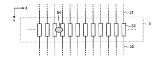
図3は、表示基板と回路基板とのFOG実装部の一例を示す図である。図3では、FOG実装部5において、表示基板1の第1配線51と回路基板2の第2配線52とが接続された接続端子53がX方向に並び配列された例を示している。
FIG. 3 is a diagram showing an example of a FOG mounting unit of a display board and a circuit board. FIG. 3 shows an example in which the
第1配線51は、一端が信号選択回路14(図4参照)に電気的に接続されている。第2配線52は、一端がドライバIC6に電気的に接続されている。図3に示す例において、FOG実装部5は、第1配線51の他端と第2配線52の他端とが電気的に接続され、複数の接続端子53が一列に並び構成されている。
One end of the
回路基板2を表示基板1にFOG実装する際、表示基板1と回路基板2との間に導電性の異物54を噛み込み、FOG実装部5において隣り合う接続端子53間で短絡が発生する可能性がある。表示部11の高精細化に伴い、FOG実装部5における接続端子53の間隔が狭くなる傾向にあり、FOG実装部5において隣り合う接続端子53間で導電性の異物54による短絡が発生する可能性が高くなる。また、導電性の異物54による短絡が高抵抗となった場合、通常検査での除去が難しいため、表示装置100の出荷品質が低下する可能性がある。なお、通常検査には表示状態を目視にて行う検査(目視検査)も含まれる。
When the
本実施形態では、表示装置100の出荷検査において、電気的な手法を用いて、FOG実装部5において隣り合う接続端子53間での短絡不良を検知する。以下、FOG実装部5において隣り合う接続端子53間の短絡不良を検出するための構成について説明する。
In the present embodiment, in the shipping inspection of the
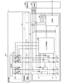
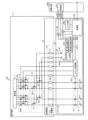
図4は、実施形態1に係る表示装置及び検査治具の概略構成を示す図である。図4に示すように、回路基板2には、表示装置100の出荷検査において検査治具200が接続される。
FIG. 4 is a diagram showing a schematic configuration of a display device and an inspection jig according to the first embodiment. As shown in FIG. 4, the
回路基板2にFOG実装されたドライバIC6は、映像線駆動回路61と、スイッチ制御部62と、出力制御回路63と、を含む。映像線駆動回路61が、本開示における「駆動回路」に対応する。
The
映像線駆動回路61は、表示動作を行う際、R(赤)、G(緑)及びB(青)の副画素SPixに供給される画素信号Vpixが時分割多重化された画像信号Vsigを生成して出力する。映像線駆動回路61は、n列(nは、正の整数)の画素列に対応するn個のアンプ回路611,・・・,61nを備えている。映像線駆動回路61は、検査治具200の電源部201から、第1正極性電源電圧AVDD1及び第1負極性電源電圧AVEE1が供給される。
The video
出力制御回路63は、映像線駆動回路61の各アンプ回路611,・・・,61nとFOG実装部5の各接続端子53との接続と遮断とを切り換える。出力制御回路63は、映像線駆動回路61の各アンプ回路611,・・・,61nにそれぞれ対応するスイッチ631,・・・,63nを備えている。なお、本実施形態では、出力制御回路63を介して映像線駆動回路61の各アンプ回路611,・・・,61nに接続される接続端子53を、短絡不良の検出対象としている。以下、本実施形態において短絡不良の検出対象とする接続端子53を、「短絡検出対象接続端子53a」と称する。
The
スイッチ制御部62は、出力制御回路63の各スイッチ及び表示基板1に設けられる信号選択回路14の各スイッチを制御する。
The
表示基板1は、画像信号Vsigに時分割多重化されたR(赤)、G(緑)及びB(青)の画素信号Vpixを分離する信号選択回路14を備えている。信号選択回路14は、例えばマルチプレクサ(MPX)を用いて構成される。
The
検査治具200は、表示装置100の出荷検査において回路基板2に接続される。検査治具200は、電源部201と、処理部202と、レジスタ部203と、電流検出部204と、を含む。
The
電源部201は、ドライバIC6に供給する第1正極性電源電圧AVDD1及び第1負極性電源電圧AVEE1を生成する。第1正極性電源電圧AVDD1は、基準電位GNDに対して、例えば+5.5Vの電位差を有している。第1負極性電源電圧AVEE1は、基準電位GNDに対して、例えば-5.5Vの電位差を有している。
The
映像線駆動回路61の各アンプ回路611,・・・,61nには、第1正極性電源電圧AVDD1、基準電位GND、及び第1負極性電源電圧AVEE1が供給される。映像線駆動回路61の各アンプ回路611,・・・,61nは、正極性の電圧を出力する際に第1正極性電源電圧AVDD1と基準電位GNDとの電位差により動作し、負極性の電圧を出力する際に基準電位GNDと第1負極性電源電圧AVEE1との電位差により動作する。なお、第1正極性電源電圧AVDD1及び第1負極性電源電圧AVEE1の基準電位GNDに対する電位差により本開示が限定されるものではない。また、本実施形態では、基準電位をGND電位としたが、これに限定されない。
A first positive electrode power supply voltage A VDD1, a reference potential GND, and a first negative electrode power supply voltage AVEE1 are supplied to each of the
処理部202は、表示装置100の出荷検査において、ドライバIC6の制御及びFOG実装部5における短絡判定処理を行う。本実施形態における短絡判定処理については後述する。
The
レジスタ部203は、処理部202によるFOG実装部5の短絡判定処理における各種データを格納する。レジスタ部203に記憶される各種データは、例えば、短絡判定処理における電流閾値、中間処理データ、及び判定フラグ等を含む。なお、レジスタ部203に記憶される各種データは、数値データであっても良いし、デジタルデータ等の離散値であっても良い。
The
電流検出部204は、電源部201に流れる電流を検出する。なお、図4では、第1正極性電源電圧AVDD1の供給経路と第1負極性電源電圧AVEE1の供給経路との双方に電流検出器を設ける構成を示したが、第1正極性電源電圧AVDD1の供給経路及び第1負極性電源電圧AVEE1の供給経路の少なくとも何れか一方に流れる電流を検出する構成であっても良い。
The
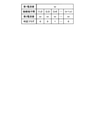
以下、上述した構成において、FOG実装部5における短絡判定処理を行う手順について説明する。図5は、実施形態1に係る短絡判定処理手順の一例を示す図である。図6は、実施形態1に係る短絡判定処理においてレジスタ部に格納される情報の一例を示す図である。
Hereinafter, in the above-described configuration, the procedure for performing the short-circuit determination process in the
図5に示す短絡判定処理は、あらかじめ回路基板2に検査治具200が接続され、電源部201から第1正極性電源電圧AVDD1及び第1負極性電源電圧AVEE1が供給された状態で開始される。なお、本短絡判定処理における判定結果を示す判定フラグは「0」に設定され、レジスタ部203に格納されているものとする。ここで、判定フラグ「0」は、FOG実装部5の何れの短絡検出対象接続端子53a間においても短絡が発生していないことを示し、判定フラグ「1」は、FOG実装部5の1以上の短絡検出対象接続端子53a間において短絡が発生していることを示すものとする。
The short-circuit determination process shown in FIG. 5 is started in a state where the
短絡判定処理開始指令が入力されると、処理部202は、スイッチ制御部62に対し、出力制御回路63の全スイッチの閉制御指令、及び、信号選択回路14の全スイッチの開制御指令を出力する(ステップS101)。これにより、映像線駆動回路61とFOG実装部5の短絡検出対象接続端子53aとの間の配線が接続され、表示部11の映像信号線SGLとFOG実装部5の短絡検出対象接続端子53aとの間の配線が遮断される。図4における信号選択回路14及び映像線駆動回路61の各スイッチの状態は、ステップS101の処理を実施した状態を示している。
When the short-circuit determination processing start command is input, the
続いて、処理部202は、映像線駆動回路61に対し、FOG実装部5において隣り合う短絡検出対象接続端子53a間の電位差が略ゼロとなるように制御する(ステップS102)。具体的には、奇数列の短絡検出対象接続端子53aに対応する各アンプ回路から、例えば0Vの直流電圧が出力されるように制御し、偶数列の短絡検出対象接続端子53aに対応する各アンプ回路から、例えば0Vの直流電圧が出力されるように制御する。このとき、FOG実装部5において隣り合う短絡検出対象接続端子53a間の電位差は0Vとなる。このときのドライバIC6の制御状態が、本開示における「第1制御状態」に対応する。処理部202は、このときの電流値を第1電流値I1として電流検出部204から取得し、第1電流値情報としてレジスタ部203に格納する(ステップS103)。
Subsequently, the
また、処理部202は、映像線駆動回路61に対し、FOG実装部5において隣り合う短絡検出対象接続端子53a間に所定の電位差を印加するように制御する(ステップS104)。具体的には、奇数列の画素Pixに画像信号Vsigを供給する各アンプ回路から、例えば+5Vの直流電圧が出力されるように制御し、偶数列の画素Pixに画像信号Vsigを供給する各アンプ回路から、例えば-5Vの直流電圧が出力されるように制御する。このとき、FOG実装部5において隣り合う短絡検出対象接続端子53a間の電位差は10Vとなる。このときのドライバIC6の制御状態が、本開示における「第2制御状態」に対応する。処理部202は、このときの電流値を第2電流値I2として電流検出部204から取得し、第2電流値情報としてレジスタ部203に格納する(ステップS105)。
Further, the
なお、図6に示す例では、第1電流値情報及び第2電流値情報をそれぞれ唯一格納した例を示したが、図4に示すように、第1正極性電源電圧AVDD1の供給経路と第1負極性電源電圧AVEE1の供給経路との双方に電流検出器を設けた場合には、第1正極性電源電圧AVDD1の供給経路に流れる電流及び第1負極性電源電圧AVEE1の供給経路に流れる電流のそれぞれに対応する第1電流値I1及び第2電流値I2を取得して第1電流値情報及び第2電流値情報を格納する態様であっても良い。 In the example shown in FIG. 6, the first current value information and the second current value information are stored only, respectively, but as shown in FIG. 4, the supply path of the first positive power supply voltage A VDD1 and the second current value information are stored. 1 When a current detector is provided in both the supply path of the negative power supply voltage AVEE1, the current flowing in the supply path of the first positive power supply voltage A VDD1 and the current flowing in the supply path of the first negative power supply voltage AVEE1. The first current value I1 and the second current value I2 corresponding to each of the above may be acquired and the first current value information and the second current value information may be stored.
なお、上述したステップS102及びステップS103の処理と、ステップS104及びステップS105の処理とは、入れ換えが可能である。すなわち、ステップS104及びステップS105の処理を実施してから、ステップS102及びステップS103の処理を実施する態様であっても良い。ステップS102及びステップS103の処理と、ステップS104及びステップS105の処理との実施順により本開示が限定されるものではない。 The above-mentioned processes of steps S102 and S103 and the processes of steps S104 and S105 can be interchanged. That is, there may be an embodiment in which the processing of step S104 and step S105 is performed, and then the processing of step S102 and step S103 is performed. The present disclosure is not limited by the order of implementation of the processes of steps S102 and S103 and the processes of steps S104 and S105.
続いて、処理部202は、レジスタ部203から第1電流値情報と第2電流値情報とを読み出し、第1電流値I1と第2電流値I2との差分|I1-I2|を電流閾値ΔIthと比較する(|I1-I2|>ΔIth)(ステップS106)。ここで、第1正極性電源電圧AVDD1の供給経路に流れる電流及び第1負極性電源電圧AVEE1の供給経路に流れる電流のそれぞれに対応する第1電流値I1及び第2電流値I2を取得した場合には、第1正極性電源電圧AVDD1の供給経路に流れる電流及び第1負極性電源電圧AVEE1の供給経路に流れる電流のそれぞれに対し、ステップS106の処理を行う。
Subsequently, the
第1電流値I1と第2電流値I2との差分|I1-I2|が電流閾値ΔIthよりも大きい場合(ステップS106;Yes)、処理部202は、FOG実装部5の1以上の短絡検出対象接続端子53a間において短絡が発生しているものと判定し、レジスタ部203の判定フラグを「0」から「1」に書き換えて(ステップS107)、実施形態1に係る短絡判定処理を終了する。図6では、FOG実装部5の1以上の短絡検出対象接続端子53a間において短絡が発生した例を示している。なお、第1正極性電源電圧AVDD1の供給経路に流れる電流及び第1負極性電源電圧AVEE1の供給経路に流れる電流のそれぞれに対応する第1電流値I1及び第2電流値I2を取得した場合には、処理部202は、ステップS106の処理において、少なくとも一方の処理結果が電流閾値よりも大きい場合に、FOG実装部5の1以上の短絡検出対象接続端子53a間において短絡が発生しているものと判定する態様であっても良い。
When the difference | I1-I2 | between the first current value I1 and the second current value I2 is larger than the current threshold value ΔIt (step S106; Yes), the
第1電流値I1と第2電流値I2との差分|I1-I2|が電流閾値ΔIth以下である場合(ステップS106;No)、処理部202は、FOG実装部5の何れの短絡検出対象接続端子53a間においても短絡が発生していないものと判定し、実施形態1に係る短絡判定処理を終了する。
When the difference | I1-I2 | between the first current value I1 and the second current value I2 is equal to or less than the current threshold value ΔIth (step S106; No), the
上述した実施形態1に係る構成において、実施形態1に係る短絡判定処理手順を実施することにより、FOG実装部5の1以上の短絡検出対象接続端子53a間において短絡が発生していること検知することができる。そして、レジスタ部203の判定フラグを外部から処理部202を介して読み出すことで、FOG実装部5の何れかの短絡検出対象接続端子53a間において短絡が発生しているか否かを識別することができる。
In the configuration according to the first embodiment described above, by carrying out the short circuit determination processing procedure according to the first embodiment, it is detected that a short circuit has occurred between one or more short circuit detection
(実施形態1の変形例1)
図7は、実施形態1の変形例1に係る短絡判定処理手順の一例を示す図である。図8は、実施形態1の変形例1に係る短絡判定処理においてレジスタ部に格納される情報の一例を示す図である。
(
FIG. 7 is a diagram showing an example of the short-circuit determination processing procedure according to the first modification of the first embodiment. FIG. 8 is a diagram showing an example of information stored in the register unit in the short circuit determination process according to the first modification of the first embodiment.
図7に示す短絡判定処理は、あらかじめ回路基板2に検査治具200が接続され、電源部201から第1正極性電源電圧AVDD1及び第1負極性電源電圧AVEE1が供給された状態で開始される。
The short-circuit determination process shown in FIG. 7 is started in a state where the
短絡判定処理開始指令が入力されると、処理部202は、スイッチ制御部62に対し、出力制御回路63の全スイッチの閉制御指令、及び、信号選択回路14の全スイッチの開制御指令を出力する(ステップS201)。これにより、映像線駆動回路61とFOG実装部5の短絡検出対象接続端子53aとの間の配線が接続され、表示部11の映像信号線SGLとFOG実装部5の短絡検出対象接続端子53aとの間の配線が遮断される。図4における信号選択回路14及び映像線駆動回路61の各スイッチの状態は、ステップS201の処理を実施した状態を示している。
When the short-circuit determination processing start command is input, the
続いて、処理部202は、映像線駆動回路61に対し、FOG実装部5において隣り合う短絡検出対象接続端子53a間の電位差が略ゼロとなるように制御する(ステップS202)。具体的には、奇数列の短絡検出対象接続端子53aに対応する各アンプ回路から、例えば0Vの直流電圧が出力されるように制御し、偶数列の短絡検出対象接続端子53aに対応する各アンプ回路から、例えば0Vの直流電圧が出力されるように制御する。このとき、FOG実装部5において隣り合う短絡検出対象接続端子53a間の電位差は0Vとなる。このときのドライバIC6の制御状態が、本開示における「第1制御状態」に対応する。処理部202は、このときの電流値を第1電流値I1として電流検出部204から取得し、第1電流値情報としてレジスタ部203に格納する(ステップS203)。
Subsequently, the
続いて、処理部202は、FOG実装部5において隣り合う短絡検出対象接続端子53aのうち、任意の短絡検出対象接続端子53a間を選択する(ステップS204)。画素列の数がn列であるとき、隣り合う短絡検出対象接続端子53aの組み合わせは、n-1通りである。
Subsequently, the
処理部202は、映像線駆動回路61に対し、選択した短絡検出対象接続端子53a間に所定の電位差を印加するように制御する(ステップS205)。具体的には、選択した短絡検出対象接続端子53a間において、奇数列の画素Pixに画像信号Vsigを供給するアンプ回路から、例えば+5Vの直流電圧が出力されるように制御し、選択した短絡検出対象接続端子53a間において、偶数列の画素Pixに画像信号Vsigを供給するアンプ回路から、例えば-5Vの直流電圧が出力されるように制御する。このとき、選択した短絡検出対象接続端子53a間の電位差は10Vとなる。このときのドライバIC6の制御状態が、本開示における「第2制御状態」に対応する。処理部202は、このときの電流値を第2電流値I2として電流検出部204から取得し、第2電流値情報としてレジスタ部203に格納する(ステップS206)。
The
続いて、処理部202は、レジスタ部203から第1電流値情報と選択した短絡検出対象接続端子53a間における第2電流値情報とを読み出し、第1電流値I1と第2電流値I2との差分|I1-I2|を電流閾値ΔIthと比較する(|I1-I2|>ΔIth)(ステップS207)。
Subsequently, the
第1電流値I1と第2電流値I2との差分|I1-I2|が電流閾値ΔIthよりも大きい場合(ステップS207;Yes)、処理部202は、選択した短絡検出対象接続端子53a間において短絡が発生しているものと判定し、レジスタ部203の判定フラグを「0」から「1」に書き換える(ステップS208)。図8では、短絡検出対象接続端子53a間(3,4)において短絡が発生した例を示している。
When the difference | I1-I2 | between the first current value I1 and the second current value I2 is larger than the current threshold value ΔIt (step S207; Yes), the
第1電流値I1と第2電流値I2との差分|I1-I2|が電流閾値ΔIth以下である場合(ステップS207;No)、処理部202は、選択した短絡検出対象接続端子53a間において短絡が発生していないものと判定する。
When the difference | I1-I2 | between the first current value I1 and the second current value I2 is equal to or less than the current threshold value ΔIth (step S207; No), the
続いて、処理部202は、隣り合う全ての短絡検出対象接続端子53a間(1,2),(2,3),(3,4),・・・(n-1,n)において短絡判定済みであるか否かを判定する(ステップS209)。
Subsequently, the
短絡判定済みでない短絡検出対象接続端子53a間があれば(ステップS209;No)、ステップS204に戻り、ステップS209までの処理を繰り返し実施する。
If there is a short-circuit detection
全ての短絡検出対象接続端子53a間において短絡判定済みであれば(ステップS209;Yes)、実施形態1の変形例1に係る短絡判定処理を終了する。
If the short-circuit determination has been completed between all the short-circuit detection
上述した実施形態1に係る構成において、実施形態1の変形例1に係る短絡判定処理手順を実施することにより、FOG実装部5において短絡が発生している短絡検出対象接続端子53a間を特定することができる。そして、レジスタ部203の情報を外部から処理部202を介して読み出すことで、FOG実装部5において短絡が発生している短絡検出対象接続端子53a間を識別することができる。
In the configuration according to the first embodiment described above, by carrying out the short-circuit determination processing procedure according to the first modification of the first embodiment, the short-circuit detection
なお、本実施形態では、第2制御状態において、奇数列の画素Pixに画像信号Vsigを供給する各アンプ回路から、例えば+5Vの直流電圧が出力されるように制御し、偶数列の画素Pixに画像信号Vsigを供給する各アンプ回路から、例えば-5Vの直流電圧が出力されるように制御する例を示したが、以下のような態様とすることも可能である。 In this embodiment, in the second control state, control is performed so that, for example, a DC voltage of + 5V is output from each amplifier circuit that supplies the image signal Vsig to the pixel Pix in the odd row, and the pixel Pix in the even row is used. An example of controlling so that a DC voltage of, for example, -5V is output from each amplifier circuit that supplies the image signal Vsig is shown, but the following aspects are also possible.
例えば、第2制御状態において、奇数列の画素Pixに画像信号Vsigを供給する各アンプ回路から、例えば-5Vの直流電圧が出力されるように制御し、偶数列の画素Pixに画像信号Vsigを供給する各アンプ回路から、例えば+5Vの直流電圧が出力されるように制御する態様であっても良い。 For example, in the second control state, control is performed so that, for example, a DC voltage of -5V is output from each amplifier circuit that supplies the image signal Vsig to the pixel Pix in the odd row, and the image signal Vsig is output to the pixel Pix in the even row. A mode may be used in which control is performed so that, for example, a DC voltage of + 5 V is output from each of the supplied amplifier circuits.
例えば、第2制御状態において、奇数列の画素Pixに画像信号Vsigを供給する各アンプ回路から、例えば+5Vの直流電圧が出力されるように制御し、偶数列の画素Pixに画像信号Vsigを供給する各アンプ回路から、例えば0Vの直流電圧が出力されるように制御する態様であっても良い。 For example, in the second control state, each amplifier circuit that supplies the image signal Vsig to the odd-row pixels Pix is controlled so that a DC voltage of, for example, + 5V is output, and the image signal Vsig is supplied to the even-row pixels Pix. A mode may be used in which control is performed so that, for example, a DC voltage of 0 V is output from each of the amplifier circuits.
また、例えば、第2制御状態において、奇数列の画素Pixに画像信号Vsigを供給する各アンプ回路から、例えば0Vの直流電圧が出力されるように制御し、偶数列の画素Pixに画像信号Vsigを供給する各アンプ回路から、例えば-5Vの直流電圧が出力されるように制御する態様であっても良い。 Further, for example, in the second control state, control is performed so that, for example, a DC voltage of 0 V is output from each amplifier circuit that supplies the image signal Vsig to the pixel Pix in the odd row, and the image signal Vsig is output to the pixel Pix in the even row. The amplifier circuit may be controlled so that a DC voltage of, for example, -5V is output from each amplifier circuit.
すなわち、第2制御状態において、隣り合う短絡検出対象接続端子53aに異なる電圧を供給可能な態様であれば良い。
That is, in the second control state, different voltages may be supplied to the adjacent short-circuit detection
(実施形態1の変形例2)
図9は、実施形態1の変形例2に係る表示装置及び検査治具の概略構成を示す図である。なお、実施形態1と同じ構成要素には、同じ参照符号を付して、説明を省略する。
(
FIG. 9 is a diagram showing a schematic configuration of a display device and an inspection jig according to a
図9に示すように、回路基板2aには、表示装置100aの出荷検査において検査治具200aが接続される。
As shown in FIG. 9, the
回路基板2aにFOG実装されたドライバIC6aは、映像線駆動回路61と、スイッチ制御部62と、出力制御回路63と、処理部65と、レジスタ部66と、電流検出部67と、を含む。
The
処理部65は、実施形態1の検査治具200における処理部202に相当する構成部であり、表示装置100aの出荷検査において、ドライバIC6aの制御及びFOG実装部5における短絡判定処理を行う。
The
レジスタ部66は、実施形態1の検査治具200におけるレジスタ部203に相当する構成部であり、処理部65によるFOG実装部5の短絡判定処理における各種データを格納する。レジスタ部66に記憶される各種データは、例えば、短絡判定処理における閾値、中間処理データ、及び判定フラグ等を含む。なお、レジスタ部66に記憶される各種データは、数値データであっても良いし、デジタルデータ等の離散値であっても良い。
The
電流検出部67は、実施形態1の検査治具200における電流検出部204に相当する構成部である。
The
検査治具200aは、表示装置100aの出荷検査において回路基板2aに接続される。検査治具200aは、電源部201を含む。
The
上述した構成において、FOG実装部5における短絡判定処理を行う手順については、実施形態1に係る短絡判定処理手順及び実施形態1の変形例1に係る短絡判定処理手順と同様である。具体的には、実施形態1に係る短絡判定処理手順及び実施形態1の変形例1に係る短絡判定処理手順において、処理部202を処理部65に読み替え、レジスタ部203をレジスタ部66に読み替え、電流検出部204を電流検出部67に読み替えることで、実施形態1に係る短絡判定処理手順又は実施形態1の変形例1に係る短絡判定処理手順と同様の処理手順を実現することができる。
In the above-described configuration, the procedure for performing the short-circuit determination process in the
上述した実施形態1の変形例2に係る構成において、実施形態1に係る短絡判定処理手順を実施することにより、FOG実装部5の1以上の短絡検出対象接続端子53a間において短絡が発生していること検知することができる。そして、レジスタ部66の判定フラグを外部から処理部65を介して読み出すことで、FOG実装部5の何れかの短絡検出対象接続端子53a間において短絡が発生しているか否かを識別することができる。
In the configuration according to the second modification of the first embodiment described above, by carrying out the short circuit determination processing procedure according to the first embodiment, a short circuit occurs between one or more short circuit detection
また、上述した実施形態1の変形例2に係る構成において、実施形態1の変形例1に係る短絡判定処理手順を実施することにより、FOG実装部5において短絡が発生している短絡検出対象接続端子53a間を特定することができる。そして、レジスタ部66の情報を外部から処理部65を介して読み出すことで、FOG実装部5において短絡が発生している短絡検出対象接続端子53a間を識別することができる。
Further, in the configuration according to the
本実施形態により、品質を向上することができる表示装置100,100aを提供することができる。
According to this embodiment, it is possible to provide
(実施形態2)
図10Aは、実施形態2に係る表示装置及び検査治具の概略構成を示す図である。なお、実施形態1と同じ構成要素には、同じ参照符号を付して、説明を省略する。
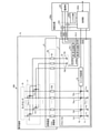
(Embodiment 2)
FIG. 10A is a diagram showing a schematic configuration of a display device and an inspection jig according to the second embodiment. The same components as those in the first embodiment are designated by the same reference numerals, and the description thereof will be omitted.
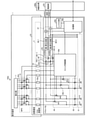
図10Aに示すように、回路基板2bには、表示装置100bの出荷検査において検査治具200bが接続される。
As shown in FIG. 10A, the
回路基板2bにFOG実装されたドライバIC6bは、映像線駆動回路61と、スイッチ制御部62aと、出力制御回路63と、電圧印加回路64と、を含む。
The
電圧印加回路64は、映像線駆動回路61の各アンプ回路611,・・・,61nにそれぞれ対応するスイッチ641,・・・,64nを備えている。電圧印加回路64は、映像線駆動回路61の各アンプ回路611,・・・,61nのうち、奇数列の画素Pixに画像信号Vsigを供給するアンプ回路に接続される短絡検出対象接続端子53aに対して個別に第1正極性電圧AVDD1を印加するスイッチ64p(pは、n以下の正の奇数)と、偶数列の画素Pixに画像信号Vsigを供給するアンプ回路に接続される短絡検出対象接続端子53aに対して個別に第1負極性電圧AVEE1を印加するスイッチ64q(qは、n以下の正の偶数)と、を含む。
The
スイッチ制御部62aは、出力制御回路63の各スイッチ、表示基板1に設けられる信号選択回路14の各スイッチに加え、電圧印加回路64の各スイッチ64p及び各スイッチ64qを制御する。
The
検査治具200bは、表示装置100bの出荷検査において回路基板2bに接続される。検査治具200bは、電源部201と、処理部202aと、レジスタ部203aと、電流検出部204と、を含む。
The
処理部202aは、表示装置100bの出荷検査において、ドライバIC6bの制御及びFOG実装部5における短絡判定処理を行う。本実施形態における短絡判定処理については後述する。
The
レジスタ部203aは、処理部202aによるFOG実装部5の短絡判定処理における各種データを格納する。レジスタ部203aに記憶される各種データは、例えば、短絡判定処理における電流閾値、中間処理データ、及び判定フラグ等を含む。なお、レジスタ部203aに記憶される各種データは、数値データであっても良いし、デジタルデータ等の離散値であっても良い。
The
以下、上述した構成において、FOG実装部5における短絡判定処理を行う手順について説明する。図11は、実施形態2に係る短絡判定処理手順の一例を示す図である。図12は、実施形態2に係る短絡判定処理においてレジスタ部に格納される情報の一例を示す図である。
Hereinafter, in the above-described configuration, the procedure for performing the short-circuit determination process in the
図11に示す短絡判定処理は、あらかじめ回路基板2bに検査治具200bが接続され、電源部201から第1正極性電源電圧AVDD1及び第1負極性電源電圧AVEE1が供給された状態で開始される。また、このとき、電圧印加回路64の全スイッチが開制御され、FOG実装部5の全ての短絡検出対象接続端子53aへの第1正極性電源電圧AVDD1又は第1負極性電源電圧AVEE1の供給が遮断されているものとする。
The short-circuit determination process shown in FIG. 11 is started in a state where the
短絡判定処理開始指令が入力されると、処理部202aは、スイッチ制御部62aに対し、出力制御回路63の全スイッチの開制御指令、及び信号選択回路14の全スイッチの開制御指令を出力する(ステップS301)。これにより、映像線駆動回路61とFOG実装部5の短絡検出対象接続端子53aとの間の配線が遮断され、表示部11の映像信号線SGLとFOG実装部5の短絡検出対象接続端子53aとの間の配線が遮断される。このときのドライバIC6bの制御状態が、本開示における「第1制御状態」に対応する。処理部202aは、このときの電流値を第1電流値I1として電流検出部204から取得し、第1電流値情報としてレジスタ部203aに格納する(ステップS302)。
When the short-circuit determination processing start command is input, the
続いて、処理部202aは、FOG実装部5において隣り合う短絡検出対象接続端子53aのうち、任意の短絡検出対象接続端子53a間を選択する(ステップS303)。画素列の数がn列であるとき、隣り合う短絡検出対象接続端子53aの組み合わせは、n-1通りである。
Subsequently, the
処理部202aは、選択した隣り合う短絡検出対象接続端子53aの一方に第1正極性電源電圧AVDD1が印加され、他方に第1負極性電源電圧AVEE1が印加されるように、電圧印加回路64のスイッチ64pとスイッチ64qとを閉制御する(ステップS304)。このとき、第1正極性電源電圧AVDD1が例えば+5.5Vであり、第1負極性電源電圧AVEE1が例えば-5.5Vである場合、隣り合う短絡検出対象接続端子53a間に印加される電位差は11Vである。図10Aにおける信号選択回路14、映像線駆動回路61、及び電圧印加回路64の各スイッチの状態は、ステップS304の処理を実施した状態を示している。図10Aに示す例では、図11に示す短絡検出対象接続端子53a間(1,2)が選択され、電圧印加回路64のスイッチ641とスイッチ642とが閉制御された例を示している。このときのドライバIC6bの制御状態が、本開示における「第2制御状態」に対応する。処理部202aは、このときの電流値を第2電流値I2として電流検出部204から取得し、第2電流値情報としてレジスタ部203aに格納する(ステップS305)。
The
続いて、処理部202aは、レジスタ部203aから第1電流値情報と選択した短絡検出対象接続端子53a間における第2電流値情報とを読み出し、第1電流値I1と第2電流値I2との差分|I1-I2|を電流閾値ΔIthと比較する(|I1-I2|>ΔIth)(ステップS306)。
Subsequently, the
第1電流値I1と第2電流値I2との差分|I1-I2|が電流閾値ΔIthよりも大きい場合(ステップS306;Yes)、処理部202aは、選択した短絡検出対象接続端子53a間において短絡が発生しているものと判定し、当該短絡検出対象接続端子53a間におけるレジスタ部203aの判定フラグを「0」から「1」に書き換える(ステップS307)。図12では、短絡検出対象接続端子53a間(3,4)において短絡が発生した例を示している。
When the difference | I1-I2 | between the first current value I1 and the second current value I2 is larger than the current threshold value ΔIt (step S306; Yes), the
第1電流値I1と第2電流値I2との差分|I1-I2|が電流閾値ΔIth以下である場合(ステップS306;No)、処理部202aは、選択した短絡検出対象接続端子53a間において短絡が発生していないものと判定する。
When the difference | I1-I2 | between the first current value I1 and the second current value I2 is equal to or less than the current threshold value ΔIth (step S306; No), the
続いて、処理部202aは、隣り合う全ての短絡検出対象接続端子53a間(1,2),(2,3),(3,4),・・・(n-1,n)において短絡判定済みであるか否かを判定する(ステップS308)。
Subsequently, the
短絡判定済みでない短絡検出対象接続端子53a間があれば(ステップS308;No)、ステップS303に戻り、ステップS308までの処理を繰り返し実施する。
If there is a short-circuit detection
全ての短絡検出対象接続端子53a間において短絡判定済みであれば(ステップS308;Yes)、実施形態2に係る短絡判定処理を終了する。
If the short-circuit determination has been completed between all the short-circuit detection
上述した実施形態2に係る構成において、実施形態2に係る短絡判定処理手順を実施することにより、実施形態1の変形例1と同様に、FOG実装部5において短絡が発生している短絡検出対象接続端子53a間を特定することができる。そして、レジスタ部203aの情報を外部から処理部202aを介して読み出すことで、FOG実装部5において短絡が発生している短絡検出対象接続端子53a間を識別することができる。
In the configuration according to the second embodiment described above, by carrying out the short circuit determination processing procedure according to the second embodiment, a short circuit detection target in which a short circuit occurs in the
また、映像線駆動回路61の各アンプ回路611,・・・,61nの動作を停止させることができるので、第1電流値I1及び第2電流値I2に含まれる定常的な回路電流を小さくすることができ、短絡判定を行う際の閾値判定の精度が向上する。
Further, since the operation of each of the
なお、本実施形態では、電圧印加回路64のスイッチ64p(pは、n以下の正の奇数)が奇数列の画素Pixに画像信号Vsigを供給するアンプ回路に接続される短絡検出対象接続端子53aに対して個別に第1正極性電圧AVDD1を印加し、電圧印加回路64のスイッチ64q(qは、n以下の正の偶数)が偶数列の画素Pixに画像信号Vsigを供給するアンプ回路に接続される短絡検出対象接続端子53aに対して個別に第1負極性電圧AVEE1を印加する例を示したが、以下のような態様とすることも可能である。
In the present embodiment, the switch 64p (p is a positive odd number of n or less) of the
図10Bは、実施形態2に係る表示装置及び検査治具の概略構成における第1変形例を示す図である。図10Bに示すように、例えば、電圧印加回路64のスイッチ64p(pは、n以下の正の奇数)が奇数列の画素Pixに画像信号Vsigを供給するアンプ回路に接続される短絡検出対象接続端子53aに対して個別に第1負極性電圧AVEE1を印加し、電圧印加回路64のスイッチ64q(qは、n以下の正の偶数)が偶数列の画素Pixに画像信号Vsigを供給するアンプ回路に接続される短絡検出対象接続端子53aに対して個別に第1正極性電圧AVDD1を印加する態様であっても良い。
FIG. 10B is a diagram showing a first modification in the schematic configuration of the display device and the inspection jig according to the second embodiment. As shown in FIG. 10B, for example, a short-circuit detection target connection in which a switch 64p (p is a positive odd number of n or less) of the
図10Cは、実施形態2に係る表示装置及び検査治具の概略構成における第2変形例を示す図である。図10Cに示すように、例えば、電圧印加回路64のスイッチ64p(pは、n以下の正の奇数)が奇数列の画素Pixに画像信号Vsigを供給するアンプ回路に接続される短絡検出対象接続端子53aに対して個別に第1正極性電圧AVDD1を印加し、電圧印加回路64のスイッチ64q(qは、n以下の正の偶数)が偶数列の画素Pixに画像信号Vsigを供給するアンプ回路に接続される短絡検出対象接続端子53aに対して個別に基準電位GNDを印加する態様であっても良い。
FIG. 10C is a diagram showing a second modification in the schematic configuration of the display device and the inspection jig according to the second embodiment. As shown in FIG. 10C, for example, a short-circuit detection target connection in which a switch 64p (p is a positive odd number of n or less) of the
図10Dは、実施形態2に係る表示装置及び検査治具の概略構成における第3変形例を示す図である。図10Dに示すように、例えば、電圧印加回路64のスイッチ64p(pは、n以下の正の奇数)が奇数列の画素Pixに画像信号Vsigを供給するアンプ回路に接続される短絡検出対象接続端子53aに対して個別に基準電位GNDを印加し、電圧印加回路64のスイッチ64q(qは、n以下の正の偶数)が偶数列の画素Pixに画像信号Vsigを供給するアンプ回路に接続される短絡検出対象接続端子53aに対して個別に第1負極性電圧AVEE1を印加する態様であっても良い。
FIG. 10D is a diagram showing a third modification in the schematic configuration of the display device and the inspection jig according to the second embodiment. As shown in FIG. 10D, for example, a short-circuit detection target connection in which a switch 64p (p is a positive odd number of n or less) of the
すなわち、第2制御状態において、隣り合う短絡検出対象接続端子53aに異なる電圧を供給可能な態様であれば良い。
That is, in the second control state, different voltages may be supplied to the adjacent short-circuit detection
(実施形態2の変形例)
図13は、実施形態2の変形例に係る表示装置及び検査治具の概略構成を示す図である。なお、実施形態2と同じ構成要素には、同じ参照符号を付して、説明を省略する。
(Modified Example of Embodiment 2)
FIG. 13 is a diagram showing a schematic configuration of a display device and an inspection jig according to a modified example of the second embodiment. The same components as those in the second embodiment are designated by the same reference numerals, and the description thereof will be omitted.
図13に示すように、回路基板2cには、表示装置100cの出荷検査において検査治具200aが接続される。
As shown in FIG. 13, the
回路基板2cにFOG実装されたドライバIC6cは、映像線駆動回路61と、スイッチ制御部62aと、出力制御回路63と、電圧印加回路64と、処理部65aと、レジスタ部66aと、電流検出部67と、を含む。
The driver IC 6c mounted on the circuit board 2c by FOG includes a video
処理部65aは、実施形態2の検査治具200bにおける処理部202aに相当する構成部であり、表示装置100cの出荷検査において、ドライバIC6cの制御及びFOG実装部5における短絡判定処理を行う。
The
レジスタ部66aは、実施形態2の検査治具200bにおけるレジスタ部203aに相当する構成部であり、処理部65aによるFOG実装部5の短絡判定処理における各種データを格納する。レジスタ部66aに記憶される各種データは、例えば、短絡判定処理における電流閾値、中間処理データ、及び判定フラグ等を含む。なお、レジスタ部66aに記憶される各種データは、数値データであっても良いし、デジタルデータ等の離散値であっても良い。
The
電流検出部67は、実施形態2の検査治具200bにおける電流検出部204に相当する構成部である。
The
検査治具200aは、表示装置100cの出荷検査において回路基板2cに接続される。検査治具200aは、電源部201を含む。
The
上述した構成において、FOG実装部5における短絡判定処理を行う手順については、実施形態2に係る短絡判定処理手順と同様である。具体的には、実施形態2に係る短絡判定処理手順において、処理部202aを処理部65aに読み替え、レジスタ部203aをレジスタ部66aに読み替え、電流検出部204を電流検出部67に読み替えることで、実施形態2に係る短絡判定処理手順と同様の処理手順を実現することができる。
In the above-described configuration, the procedure for performing the short-circuit determination process in the
上述した実施形態2の変形例に係る構成において、実施形態2に係る短絡判定処理手順を実施することにより、FOG実装部5において短絡が発生している短絡検出対象接続端子53a間を特定することができる。そして、レジスタ部66aの情報を外部から処理部65aを介して読み出すことで、FOG実装部5において短絡が発生している短絡検出対象接続端子53a間を識別することができる。
In the configuration according to the modification of the second embodiment described above, by carrying out the short circuit determination processing procedure according to the second embodiment, the short circuit detection
また、実施形態2と同様に、映像線駆動回路61の各アンプ回路611,・・・,61nの動作を停止させることができるので、第1電流値I1及び第2電流値I2に含まれる定常的な回路電流を小さくすることができ、短絡判定を行う際の閾値判定の精度が向上する。
Further, as in the second embodiment, since the operations of the
本実施形態により、品質を向上することができる表示装置100b,100cを提供することができる。
According to this embodiment, it is possible to provide
(実施形態3)
図14は、実施形態3に係る表示装置及び検査治具の概略構成を示す図である。なお、実施形態1又は実施形態2と同じ構成要素には、同じ参照符号を付して、説明を省略する。
(Embodiment 3)
FIG. 14 is a diagram showing a schematic configuration of a display device and an inspection jig according to the third embodiment. The same components as those in the first embodiment or the second embodiment are designated by the same reference numerals, and the description thereof will be omitted.
図14に示すように、回路基板2dには、表示装置100dの出荷検査において検査治具200aが接続される。
As shown in FIG. 14, the
回路基板2dにFOG実装されたドライバIC6dは、映像線駆動回路61と、スイッチ制御部62bと、出力制御回路63と、電圧印加回路64と、処理部65bと、レジスタ部66bと、電流検出部67と、第1昇圧回路68-1と、第2昇圧回路68-2と、電圧切換回路69と、を含む。
The
第1昇圧回路68-1は、検査治具200aの電源部201から供給される第1正極性電源電圧AVDD1を昇圧して、第2正極性電圧AVDD2を生成する。第2正極性電圧AVDD2は、例えば+10Vである。
The first booster circuit 68-1 boosts the first positive electrode power supply voltage A VDD1 supplied from the
第2昇圧回路68-2は、検査治具200aの電源部201から供給される第1負極性電源電圧AVEE1を昇圧して、第2負極性電圧AVEE2を生成する。第2負極性電圧AVEE2は、例えば-10Vである。
The second booster circuit 68-2 boosts the first negative electrode power supply voltage AVEE1 supplied from the
本実施形態では、後述する短絡判定処理の第2制御状態において、選択した隣り合う短絡検出対象接続端子53a間に第1正極性電源電圧AVDD1と第1負極性電源電圧AVEE1との電位差である第1電位差を印加し、短絡が発生している短絡検出対象接続端子53a間が発生していることを検出した場合に、当該短絡検出対象接続端子53a間に第1電位差よりも大きい第2正極性電源電圧AVDD2と第2負極性電源電圧AVEE2との電位差である第2電位差を印加することで、隣り合う短絡検出対象接続端子53a間の導電性の異物54(図3)を除去し、短絡を解消する。なお、第2正極性電源電圧AVDD2及び第2負極性電源電圧AVEE2の電圧、すなわち、第2電位差の大きさにより本開示が限定されるものではない。
In the present embodiment, in the second control state of the short-circuit determination process described later, the potential difference between the first positive power supply voltage A VDD1 and the first negative power supply voltage AVEE1 between the selected adjacent short-circuit detection
電圧切換回路69は、電圧印加回路64に供給する電源電圧を切り換える。具体的に、電圧切換回路69は、電圧印加回路64の各スイッチ64pへの第1正極性電源電圧AVDD1の供給と遮断とを切り換えるスイッチ691-1と、電圧印加回路64の各スイッチ64qへの第1負極性電源電圧AVEE1の供給と遮断とを切り換えるスイッチ691-2と、電圧印加回路64の各スイッチ64pへの第2正極性電源電圧AVDD2の供給と遮断とを切り換えるスイッチ692-1と、電圧印加回路64の各スイッチ64qへの第2負極性電源電圧AVEE2の供給と遮断とを切り換えるスイッチ692-2と、を備えている。
The
スイッチ制御部62bは、出力制御回路63の各スイッチ、表示基板1に設けられる信号選択回路14の各スイッチ、電圧印加回路64の各スイッチ64p及び各スイッチ64qに加え、電圧切換回路69の各スイッチ691-1,691-2,692-1,692-2を制御する。
The
具体的に、電圧印加回路64の各スイッチ64pに第1正極性電源電圧AVDD1を供給し、電圧印加回路64の各スイッチ64qに第1負極性電源電圧AVEE1を供給する場合には、スイッチ制御部62bは、電圧切換回路69の各スイッチ691-1,691-2を閉制御すると共に、電圧切換回路69の各スイッチ692-1,692-2を開制御する。
Specifically, when the first positive power supply voltage A VDD1 is supplied to each switch 64p of the
また、電圧印加回路64の各スイッチ64pに第2正極性電源電圧AVDD2を供給し、電圧印加回路64の各スイッチ64qに第2負極性電源電圧AVEE2を供給する場合には、スイッチ制御部62bは、電圧切換回路69の各スイッチ691-1,691-2を開制御すると共に、電圧切換回路69の各スイッチ692-1,692-2を閉制御する。
Further, when the second positive power supply voltage A00572 is supplied to each switch 64p of the
処理部65bは、表示装置100dの出荷検査において、ドライバIC6dの制御及びFOG実装部5における短絡判定処理を行う。本実施形態における短絡判定処理については後述する。
The
レジスタ部66bは、処理部65bによるFOG実装部5の短絡判定処理における各種データを格納する。レジスタ部66bに記憶される各種データは、例えば、短絡判定処理における電流閾値、中間処理データ、及び判定フラグ等を含む。なお、レジスタ部66bに記憶される各種データは、数値データであっても良いし、デジタルデータ等の離散値であっても良い。
The register unit 66b stores various data in the short-circuit determination process of the
以下、上述した構成において、FOG実装部5における短絡判定処理を行う手順について説明する。図15は、実施形態3に係る短絡判定処理手順の一例を示す図である。図16は、実施形態3に係る短絡判定処理においてレジスタ部に格納される情報の一例を示す図である。
Hereinafter, in the above-described configuration, the procedure for performing the short-circuit determination process in the
本実施形態では、判定フラグが「1」、すなわち、短絡が発生している短絡検出対象接続端子53a間が存在している場合に、判定フラグが「1」である短絡検出対象接続端子53a間に第1電位よりも高い第2電位差を印加する処理を実施することで、判定フラグが「1」である短絡検出対象接続端子53a間の短絡解消を図っている。この処理を、以下「リペア処理」とも称する。
In the present embodiment, the determination flag is "1", that is, between the short-circuit detection
図15に示す短絡判定処理は、あらかじめ回路基板2dに検査治具200aが接続され、電源部201から第1正極性電源電圧AVDD1及び第1負極性電源電圧AVEE1が供給された状態で開始される。また、このとき、電圧印加回路64の全スイッチが開制御され、FOG実装部5の全ての短絡検出対象接続端子53aへの正極性電圧又は負極性電圧の供給が遮断されているものとする。また、電圧切換回路69の各スイッチ691-1,691-2が閉制御されると共に、電圧切換回路69の各スイッチ692-1,692-2が開制御されているものとする。
The short-circuit determination process shown in FIG. 15 is started in a state where the
短絡判定処理開始指令が入力されると、処理部65bは、スイッチ制御部62bに対し、出力制御回路63の全スイッチの開制御指令、及び信号選択回路14の全スイッチの開制御指令を出力する(ステップS401)。これにより、映像線駆動回路61とFOG実装部5の短絡検出対象接続端子53aとの間の配線が遮断され、表示部11の映像信号線SGLとFOG実装部5の短絡検出対象接続端子53aとの間の配線が遮断される。このときのドライバIC6dの制御状態が、本開示における「第1制御状態」に対応する。処理部65bは、このときの電流値を第1電流値I1として電流検出部67から取得し、第1電流値情報としてレジスタ部66bに格納する(ステップS402)。
When the short-circuit determination processing start command is input, the
続いて、処理部65bは、FOG実装部5において隣り合う短絡検出対象接続端子53aのうち、任意の短絡検出対象接続端子53a間を選択する(ステップS403)。画素列の数がn列であるとき、隣り合う短絡検出対象接続端子53aの組み合わせは、n-1通りである。
Subsequently, the
処理部65bは、選択した隣り合う短絡検出対象接続端子53aの一方に第1正極性電源電圧AVDD1が印加され、他方に第1負極性電源電圧AVEE1が印加されるように、電圧印加回路64のスイッチ64pとスイッチ64qとを閉制御する(ステップS404)。このとき、第1正極性電源電圧AVDD1が例えば+5.5Vであり、第1負極性電源電圧AVEE1が例えば-5.5Vである場合、隣り合う短絡検出対象接続端子53a間に印加される第1電位差は11Vである。図14における信号選択回路14、映像線駆動回路61、電圧印加回路64、及び電圧切換回路69の各スイッチの状態は、ステップS404の処理を実施した状態を示している。図14に示す例では、図16に示す短絡検出対象接続端子53a間(1,2)が選択され、電圧印加回路64のスイッチ641とスイッチ642とが閉制御された例を示している。このときのドライバIC6dの制御状態が、本開示における「第2制御状態」に対応する。処理部65bは、このときの電流値を第2電流値I2として電流検出部67から取得し、第2電流値情報としてレジスタ部66bに格納する(ステップS405)。
The
続いて、処理部65bは、レジスタ部66bから第1電流値情報と第2電流値情報とを読み出し、第1電流値I1と第2電流値I2との差分|I1-I2|を電流閾値ΔIthと比較する(|I1-I2|>ΔIth)(ステップS406)。
Subsequently, the
第1電流値I1と第2電流値I2との差分|I1-I2|が電流閾値ΔIthよりも大きい場合(ステップS406;Yes)、処理部65bは、選択した短絡検出対象接続端子53a間において短絡が発生しているものと判定し、当該短絡検出対象接続端子53a間におけるレジスタ部66bの判定フラグを「0」から「1」に書き換える(ステップS407a)。図16では、短絡検出対象接続端子53a間(3,4)において短絡が発生した例を示している。
When the difference | I1-I2 | between the first current value I1 and the second current value I2 is larger than the current threshold value ΔIt (step S406; Yes), the
第1電流値I1と第2電流値I2との差分|I1-I2|が電流閾値ΔIth以下である場合(ステップS406;No)、処理部65bは、選択した短絡検出対象接続端子53a間において短絡が発生していないものと判定し、当該短絡検出対象接続端子53a間におけるレジスタ部66bの判定フラグが「1」である場合には、当該判定フラグを「1」から「0」に書き換える(ステップS407b)。
When the difference | I1-I2 | between the first current value I1 and the second current value I2 is equal to or less than the current threshold value ΔIth (step S406; No), the
続いて、処理部65bは、隣り合う全ての短絡検出対象接続端子53a間(1,2),(2,3),(3,4),・・・(n-1,n)において短絡判定済みであるか否かを判定する(ステップS408)。
Subsequently, the
短絡判定済みでない短絡検出対象接続端子53a間があれば(ステップS408;No)、ステップS403に戻り、ステップS408までの処理を繰り返し実施する。
If there is a short-circuit detection
全ての短絡検出対象接続端子53a間において短絡判定済みとなると(ステップS408;Yes)、処理部65bは、レジスタ部66bに格納された情報を参照し、判定フラグが「1」、すなわち、短絡が発生している短絡検出対象接続端子53a間がないか否かを判定する(ステップS409)。
When the short-circuit determination has been completed between all the short-circuit detection
短絡が発生している短絡検出対象接続端子53a間がない場合には(ステップS409;Yes)、実施形態3に係る短絡判定処理を終了する。
If there is no short-circuit detection
短絡が発生している短絡検出対象接続端子53a間がある場合には(ステップS409;No)、処理部65bは、リペア済みフラグが「0」であるか否かを判定する(ステップS410)。図16では、リペア済みフラグが「0」である例を示している。
When there is a short-circuit detection
リペア済みフラグが「1」である場合(ステップS410;No)、実施形態3に係る短絡判定処理を終了する。 When the repaired flag is "1" (step S410; No), the short-circuit determination process according to the third embodiment is terminated.
リペア済みフラグが「0」である場合(ステップS410;Yes)、処理部65bは、電圧切換回路69の各スイッチ691-1,691-2を開制御すると共に、電圧切換回路69の各スイッチ692-1,692-2を閉制御する。これにより、電圧印加回路64の各スイッチ64pに第2正極性電源電圧AVDD2が供給され、電圧印加回路64の各スイッチ64qに第2負極性電源電圧AVEE2が供給される。このとき、第2正極性電源電圧AVDD2が例えば+10Vであり、第2負極性電源電圧AVEE2が例えば-10Vである場合、スイッチ64pとスイッチ64qとの間に印加される第2電位差は20Vである。
When the repaired flag is "0" (step S410; Yes), the
処理部65bは、判定フラグが「1」である短絡検出対象接続端子53a間に第2電位差が印加されるように、電圧印加回路64の各スイッチ64p及び各スイッチ64qを制御する(ステップS411)。このステップS411における処理が、上述したリペア処理に相当する。
The
処理部65bは、所定時間経過した後、電圧印加回路64の全てのスイッチを開制御すると共に、電圧切換回路69の各スイッチ691-1,691-2を閉制御し、電圧切換回路69の各スイッチ692-1,692-2を開制御する。その後、処理部65bは、リペア済みフラグを「0」から「1」に変化させ(ステップS412)、ステップS403に戻り、ステップS410までの処理を再度実施する。
After a lapse of a predetermined time, the
上述した実施形態3に係る構成において、実施形態3に係る短絡判定処理手順を実施することにより、FOG実装部5の1以上の短絡検出対象接続端子53a間において短絡が発生していること検知することができる。そして、レジスタ部66bの判定フラグを外部から処理部65bを介して読み出すことで、FOG実装部5の何れかの短絡検出対象接続端子53a間において短絡が発生しているか否かを識別することができる。
In the configuration according to the third embodiment described above, by carrying out the short circuit determination processing procedure according to the third embodiment, it is detected that a short circuit has occurred between one or more short circuit detection
また、上述した実施形態3に係る短絡判定処理では、FOG実装部5において短絡が発生している短絡検出対象接続端子53a間に対してリペア処理を実施する。これにより、短絡判定処理におけるFOG実装部5の短絡不良を低減することができる。また、レジスタ部66bの情報を外部から処理部65bを介して読み出すことで、リペア処理の履歴を参照することができる。
Further, in the short-circuit determination process according to the third embodiment described above, the repair process is performed between the short-circuit detection
なお、本実施形態では、ステップS403からステップS410までの処理を再実行しても、短絡が発生している短絡検出対象接続端子53a間がある場合には(ステップS409;No)、ステップS410においてリペア済みフラグが「1」と判定され(ステップS410;No)、実施形態3に係る短絡判定処理を終了するようにしている。これにより、リペア処理(ステップS411)を行っても短絡が解消しない個体を排除することができるが、これに限らない。例えば、リペア済みフラグを設けず、短絡検出対象接続端子53a間の短絡が解消するまでリペア処理を繰り返し実施する態様であっても良いし、複数回リペア処理を行っても短絡検出対象接続端子53a間の短絡が解消しない場合に、短絡判定処理を終了する態様であっても良い。
In the present embodiment, even if the processes from step S403 to step S410 are re-executed, if there is a short-circuit detection
本実施形態により、品質を向上することができる表示装置100dを提供することができる。
According to this embodiment, it is possible to provide a
(実施形態4)
図17は、実施形態4に係る表示装置及び検査治具の概略構成を示す図である。なお、実施形態1から実施形態3と同じ構成要素には、同じ参照符号を付して、説明を省略する。
(Embodiment 4)
FIG. 17 is a diagram showing a schematic configuration of a display device and an inspection jig according to the fourth embodiment. The same components as those in the first to third embodiments are designated by the same reference numerals, and the description thereof will be omitted.
図17に示すように、回路基板2eには、表示装置100eの出荷検査において検査治具200cが接続される。
As shown in FIG. 17, an
回路基板2eにFOG実装されたドライバIC6eは、映像線駆動回路61と、スイッチ制御部62cと、出力制御回路63と、第1昇圧回路68-1と、第2昇圧回路68-2と、電圧生成部70と、を含む。
The
スイッチ制御部62cは、出力制御回路63の各スイッチ、表示基板1aに設けられる信号選択回路14の各スイッチに加え、表示基板1aに設けられる電圧供給回路15の各スイッチを制御する。
The
電圧生成部70は、第1電圧生成回路701と、第2電圧生成回路702と、を含む。電圧生成部70には、第1昇圧回路68-1から第2正極性電圧AVDD2が供給され、第2昇圧回路68-2から第2負極性電圧AVEE2が供給される。
The
第1電圧生成回路701は、表示基板1aに供給する0V以上の正極性電圧を生成する。
The first
第2電圧生成回路702は、表示基板1aに供給する0V以下の負極性電圧を生成する。
The second
表示基板1aは、信号選択回路14の他に、電圧供給回路15を備えている。
The
電圧供給回路15は、映像線駆動回路61の各アンプ回路611,・・・,61nにそれぞれ対応するスイッチ151,・・・,15nを備えている。電圧供給回路15は、映像線駆動回路61の各アンプ回路611,・・・,61nのうち、奇数列の画素Pixに画像信号Vsigを供給するアンプ回路に接続される短絡検出対象接続端子53aに対して電圧生成部70の第1電圧生成回路701から供給される正極性電圧を印加するスイッチ15p(pは、n以下の正の奇数)と、偶数列の画素Pixに画像信号Vsigを供給するアンプ回路に接続される短絡検出対象接続端子53aに対して電圧生成部70の第2電圧生成回路702から供給される負極性電圧を印加するスイッチ15q(qは、n以下の正の偶数)と、を含む。
The
検査治具200cは、表示装置100eの出荷検査において回路基板2eに接続される。検査治具200cは、電源部201と、処理部202bと、レジスタ部203bと、電流検出部204と、を含む。
The
処理部202bは、表示装置100eの出荷検査において、ドライバIC6eの制御及びFOG実装部5aにおける短絡判定処理を行う。本実施形態における短絡判定処理については後述する。
The
レジスタ部203bは、処理部202bによるFOG実装部5aの短絡判定処理における各種データを格納する。レジスタ部203bに記憶される各種データは、例えば、短絡判定処理における電流閾値、中間処理データ、及び判定フラグ等を含む。なお、レジスタ部203bに記憶される各種データは、数値データであっても良いし、デジタルデータ等の離散値であっても良い。
The
以下、上述した構成において、FOG実装部5aにおける短絡判定処理を行う手順について説明する。図18は、実施形態4に係る短絡判定処理手順の一例を示す図である。図19は、実施形態4に係る短絡判定処理においてレジスタ部に格納される情報の一例を示す図である。
Hereinafter, in the above-described configuration, a procedure for performing a short-circuit determination process in the
本実施形態では、判定フラグが「1」、すなわち、FOG実装部5aの1以上の短絡検出対象接続端子53a間において短絡が発生している場合に、第1電位よりも高い第2電位差を印加する処理を実施することで、FOG実装部5aにおける短絡検出対象接続端子53a間の短絡解消を図っている。この処理を、以下「リペア処理」と称する。
In the present embodiment, when the determination flag is "1", that is, when a short circuit occurs between one or more short circuit detection
図18に示す短絡判定処理は、あらかじめ回路基板2eに検査治具200cが接続され、電源部201から第1正極性電源電圧AVDD1及び第1負極性電源電圧AVEE1が供給された状態で開始される。また、電圧生成部70は、FOG実装部5aにおいて隣り合う短絡検出対象接続端子53a間に所定の第1電位差を印加するように制御されているものとする。具体的には、第1電圧生成回路701から、例えば+5Vの直流電圧が出力されるように制御され、第2電圧生成回路702から、例えば-5Vの直流電圧が出力されるように制御される。このとき、電圧供給回路15の全スイッチが開制御され、FOG実装部5aの全ての短絡検出対象接続端子53aへの正極性電圧又は負極性電圧の供給が遮断されているものとする。
The short-circuit determination process shown in FIG. 18 is started in a state where the
短絡判定処理開始指令が入力されると、処理部202bは、スイッチ制御部62cに対し、出力制御回路63の全スイッチの開制御指令、及び信号選択回路14の全スイッチの開制御指令を出力する(ステップS501)。これにより、映像線駆動回路61とFOG実装部5aの短絡検出対象接続端子53aとの間の配線が遮断され、表示部11の映像信号線SGLとFOG実装部5aの短絡検出対象接続端子53aとの間の配線が遮断される。このときのドライバIC6eの制御状態が、本開示における「第1制御状態」に対応する。
When the short-circuit determination processing start command is input, the
処理部202bは、このときの電流値を第1電流値I1として電流検出部204から取得し、第1電流値情報としてレジスタ部203bに格納する(ステップS502)。
The
続いて、処理部202bは、スイッチ制御部62cに対し、電圧供給回路15の全スイッチの閉制御指令を出力する(ステップS503)。これにより、電圧生成部70とFOG実装部5aの短絡検出対象接続端子53aとの間の配線が接続される。図17における信号選択回路14、映像線駆動回路61、電圧供給回路15の各スイッチの状態は、ステップS503の処理を実施した状態を示している。このときのドライバIC6eの制御状態が、本開示における「第2制御状態」に対応する。このとき、FOG実装部5aにおいて隣り合う短絡検出対象接続端子53a間の第1電位差は10Vとなる。処理部202bは、このときの電流値を第2電流値I2として電流検出部204から取得し、第2電流値情報としてレジスタ部203bに格納する(ステップS504)。
Subsequently, the
続いて、処理部202bは、レジスタ部203bから第1電流値情報と第2電流値情報とを読み出し、第1電流値I1と第2電流値I2との差分|I1-I2|を電流閾値ΔIthと比較する(|I1-I2|>ΔIth)(ステップS505)。
Subsequently, the
第1電流値I1と第2電流値I2との差分|I1-I2|が電流閾値ΔIthよりも大きい場合(ステップS505;Yes)、処理部202bは、FOG実装部5aの1以上の短絡検出対象接続端子53a間において短絡が発生しているものと判定してレジスタ部203bの判定フラグを「0」から「1」に書き換える(ステップS506a)。図19では、FOG実装部5aの1以上の短絡検出対象接続端子53a間において短絡が発生した例を示している。
When the difference | I1-I2 | between the first current value I1 and the second current value I2 is larger than the current threshold value ΔIt (step S505; Yes), the
第1電流値I1と第2電流値I2との差分|I1-I2|が電流閾値ΔIth以下である場合(ステップS505;No)、処理部202bは、FOG実装部5aの何れの短絡検出対象接続端子53a間においても短絡が発生していないものと判定し、レジスタ部203bの判定フラグが「1」である場合には、当該判定フラグを「1」から「0」に書き換える(ステップS506b)。
When the difference | I1-I2 | between the first current value I1 and the second current value I2 is equal to or less than the current threshold value ΔIth (step S505; No), the
続いて、処理部202bは、レジスタ部203bに格納された情報を参照し、判定フラグが「0」、すなわち、FOG実装部5aの1以上の短絡検出対象接続端子53a間において短絡が発生していないか否かを判定する(ステップS507)。
Subsequently, the
FOG実装部5aの1以上の短絡検出対象接続端子53a間において短絡が発生していない場合には(ステップS507;Yes)、実施形態4に係る短絡判定処理を終了する。
If no short circuit has occurred between one or more short-circuit detection
FOG実装部5aの1以上の短絡検出対象接続端子53a間において短絡が発生している場合には(ステップS507;No)、処理部202bは、リペア済みフラグが「0」であるか否かを判定する(ステップS508)。図19では、リペア済みフラグが「0」である例を示している。
When a short circuit has occurred between one or more short-circuit detection
リペア済みフラグが「1」である場合(ステップS508;No)、実施形態4に係る短絡判定処理を終了する。 When the repaired flag is "1" (step S508; No), the short-circuit determination process according to the fourth embodiment is terminated.
リペア済みフラグが「0」である場合(ステップS508;Yes)、処理部202bは、電圧生成部70に対し、FOG実装部5aにおいて隣り合う短絡検出対象接続端子53a間に第1電位差よりも大きい第2電位差を印加するように制御する(ステップS509)。具体的には、第1電圧生成回路701から、例えば+8Vの直流電圧が出力されるように制御し、第2電圧生成回路702から、例えば-8Vの直流電圧が出力されるように制御する。このとき、FOG実装部5aにおいて隣り合う短絡検出対象接続端子53a間の第2電位差は16Vとなる。
When the repaired flag is "0" (step S508; Yes), the
処理部202bは、所定時間経過した後、FOG実装部5aにおいて隣り合う短絡検出対象接続端子53a間に第1電位差を印加すると共に、リペア済みフラグを「0」から「1」に書き換え(ステップS510)、スイッチ制御部62cに対し、電圧供給回路15の全スイッチの開制御指令を出力する(ステップS511)。その後、ステップS502に戻り、ステップS508までの処理を再度実施する。
After a lapse of a predetermined time, the
上述した実施形態4に係る構成において、実施形態4に係る短絡判定処理手順を実施することにより、FOG実装部5aの1以上の短絡検出対象接続端子53a間において短絡が発生していること検知することができる。そして、レジスタ部203bの判定フラグを外部から処理部202bを介して読み出すことで、FOG実装部5aの何れかの短絡検出対象接続端子53a間において短絡が発生しているか否かを識別することができる。
In the configuration according to the fourth embodiment described above, by carrying out the short circuit determination processing procedure according to the fourth embodiment, it is detected that a short circuit has occurred between one or more short circuit detection
また、上述した実施形態4に係る短絡判定処理では、FOG実装部5aの1以上の短絡検出対象接続端子53a間において短絡が発生している場合にリペア処理を実施する。これにより、短絡判定処理におけるFOG実装部5aの短絡不良を低減することができる。また、レジスタ部203bの情報を外部から処理部202bを介して読み出すことで、リペア処理の履歴を参照することができる。
Further, in the short-circuit determination process according to the fourth embodiment described above, the repair process is performed when a short circuit occurs between one or more short-circuit detection
また、実施形態2と同様に、映像線駆動回路61の各アンプ回路611,・・・,61nの動作を停止させることができるので、第1電流値I1及び第2電流値I2に含まれる定常的な回路電流を小さくすることができ、短絡判定を行う際の閾値判定の精度が向上する。
Further, as in the second embodiment, since the operations of the
なお、本実施形態では、ステップS502からステップS508までの処理を再実行しても、短絡が発生している場合には(ステップS507;No)、ステップS508においてリペア済みフラグが「1」と判定され(ステップS508;No)、実施形態4に係る短絡判定処理を終了するようにしている。これにより、リペア処理(ステップS509)を行っても短絡が解消しない個体を排除することができるが、これに限らない。例えば、リペア済みフラグを設けず、短絡検出対象接続端子53a間の短絡が解消するまでリペア処理を繰り返し実施する態様であっても良いし、複数回リペア処理を行っても短絡検出対象接続端子53a間の短絡が解消しない場合に、短絡判定処理を終了する態様であっても良い。
In the present embodiment, even if the processes from step S502 to step S508 are re-executed, if a short circuit occurs (step S507; No), the repaired flag is determined to be "1" in step S508. (Step S508; No), and the short-circuit determination process according to the fourth embodiment is terminated. This makes it possible to exclude individuals whose short circuit is not resolved even if the repair process (step S509) is performed, but the present invention is not limited to this. For example, the repair process may be repeated until the short circuit between the short circuit detection
(実施形態4の変形例)
図20は、実施形態4の変形例に係る表示装置及び検査治具の概略構成を示す図である。なお、実施形態4と同じ構成要素には、同じ参照符号を付して、説明を省略する。
(Modified Example of Embodiment 4)
FIG. 20 is a diagram showing a schematic configuration of a display device and an inspection jig according to a modified example of the fourth embodiment. The same components as those in the fourth embodiment are designated by the same reference numerals, and the description thereof will be omitted.
図20に示すように、回路基板2fには、表示装置100fの出荷検査において検査治具200aが接続される。
As shown in FIG. 20, the
回路基板2fにFOG実装されたドライバIC6fは、映像線駆動回路61と、スイッチ制御部62cと、出力制御回路63と、処理部65cと、レジスタ部66cと、電流検出部67と、第1昇圧回路68-1と、第2昇圧回路68-2と、電圧生成部70と、を含む。
The
処理部65cは、実施形態4の検査治具200cにおける処理部202bに相当する構成部であり、表示装置100fの出荷検査において、ドライバIC6fの制御及びFOG実装部5aにおける短絡判定処理を行う。
The
レジスタ部66cは、実施形態4の検査治具200cにおけるレジスタ部203bに相当する構成部であり、処理部65cによるFOG実装部5aの短絡判定処理における各種データを格納する。レジスタ部66cに記憶される各種データは、例えば、短絡判定処理における電流閾値、中間処理データ、及び判定フラグ等を含む。なお、レジスタ部66cに記憶される各種データは、数値データであっても良いし、デジタルデータ等の離散値であっても良い。
The
検査治具200aは、表示装置100fの出荷検査において回路基板2fに接続される。検査治具200aは、電源部201を含む。
The
上述した構成において、FOG実装部5aにおける短絡判定処理を行う手順については、実施形態4に係る短絡判定処理手順と同様である。具体的には、実施形態4に係る短絡判定処理手順において、処理部202bを処理部65cに読み替え、レジスタ部203bをレジスタ部66cに読み替え、電流検出部204を電流検出部67に読み替えることで、実施形態4に係る短絡判定処理手順と同様の処理手順を実現することができる。
In the above-described configuration, the procedure for performing the short-circuit determination process in the
上述した実施形態4の変形例に係る構成において、実施形態4に係る短絡判定処理手順を実施することにより、FOG実装部5aの1以上の短絡検出対象接続端子53a間において短絡が発生していること検知することができる。そして、レジスタ部66cの判定フラグを外部から処理部65cを介して読み出すことで、FOG実装部5aの何れかの短絡検出対象接続端子53a間において短絡が発生しているか否かを識別することができる。
In the configuration according to the modification of the fourth embodiment described above, a short circuit is generated between one or more short circuit detection
また、上述した実施形態4に係る短絡判定処理では、FOG実装部5aにおいて短絡が発生している短絡検出対象接続端子53a間に対してリペア処理を実施する。これにより、短絡判定処理におけるFOG実装部5aの短絡不良を低減することができる。また、レジスタ部66cの情報を外部から処理部65cを介して読み出すことで、リペア処理の履歴を参照することができる。
Further, in the short-circuit determination process according to the fourth embodiment described above, the repair process is performed between the short-circuit detection
また、実施形態4と同様に、映像線駆動回路61の各アンプ回路611,・・・,61nの動作を停止させることができるので、第1電流値I1及び第2電流値I2に含まれる定常的な回路電流を小さくすることができ、短絡判定を行う際の閾値判定の精度が向上する。
Further, as in the fourth embodiment, since the operations of the
本実施形態により、品質を向上することができる表示装置100e,100fを提供することができる。
According to this embodiment, it is possible to provide
(実施形態5)
図21は、実施形態5に係る表示装置及び検査治具の概略構成を示す図である。なお、実施形態1から実施形態4と同じ構成要素には、同じ参照符号を付して、説明を省略する。
(Embodiment 5)
FIG. 21 is a diagram showing a schematic configuration of a display device and an inspection jig according to the fifth embodiment. The same components as those in the first to fourth embodiments are designated by the same reference numerals, and the description thereof will be omitted.
図21に示すように、回路基板2gには、表示装置100gの出荷検査において検査治具200dが接続される。
As shown in FIG. 21, an
回路基板2gにFOG実装されたドライバIC6gは、映像線駆動回路61と、スイッチ制御部62cと、出力制御回路63と、を含む。
The
電圧読み出し回路15aの構成は、上述した実施形態4の電圧供給回路15と同様である。本実施形態において、各スイッチ15pは、映像線駆動回路61の各アンプ回路611,・・・,61nのうち、奇数列の画素Pixに画像信号Vsigを供給するアンプ回路に接続される短絡検出対象接続端子53aの電圧を、後述する検査治具200dの処理部202cで検出するためのスイッチである。また、各スイッチ15qは、偶数列の画素Pixに画像信号Vsigを供給するアンプ回路に接続される短絡検出対象接続端子53aの電圧を、後述する検査治具200dの処理部202cで検出するためのスイッチである。
The configuration of the
検査治具200dは、表示装置100gの出荷検査において回路基板2gに接続される。検査治具200dは、電源部201と、処理部202cと、レジスタ部203cと、を含む。
The
処理部202cは、表示装置100gの出荷検査において、ドライバIC6gの制御及びFOG実装部5aにおける短絡判定処理を行う。本実施形態における短絡判定処理については後述する。
The
レジスタ部203cは、処理部202cによるFOG実装部5aの短絡判定処理における各種データを格納する。レジスタ部203cに記憶される各種データは、例えば、短絡判定処理における電圧閾値、中間処理データ、及び判定フラグ等を含む。なお、レジスタ部203cに記憶される各種データは、数値データであっても良いし、デジタルデータ等の離散値であっても良い。
The
以下、上述した構成において、FOG実装部5aにおける短絡判定処理を行う手順について説明する。図22は、実施形態5に係る短絡判定処理手順の一例を示す図である。図23は、実施形態5に係る短絡判定処理においてレジスタ部に格納される情報の一例を示す図である。
Hereinafter, in the above-described configuration, a procedure for performing a short-circuit determination process in the
図22に示す短絡判定処理は、あらかじめ回路基板2gに検査治具200dが接続され、電源部201から第1正極性電源電圧AVDD1及び第1負極性電源電圧AVEE1が供給された状態で開始される。
The short-circuit determination process shown in FIG. 22 is started in a state where the
短絡判定処理開始指令が入力されると、処理部202cは、スイッチ制御部62cに対し、出力制御回路63の全スイッチの閉制御指令、信号選択回路14の全スイッチの開制御指令、及び電圧読み出し回路15aの全スイッチの閉制御指令を出力する(ステップS601)。これにより、映像線駆動回路61とFOG実装部5aの短絡検出対象接続端子53aとの間の配線が接続され、表示部11の映像信号線SGLとFOG実装部5aの短絡検出対象接続端子53aとの間の配線が遮断され、電圧生成部70とFOG実装部5aの短絡検出対象接続端子53aとの間の配線が接続される。このときのドライバIC6gの制御状態が、本開示における「第1制御状態」に対応する。図21における信号選択回路14、映像線駆動回路61、電圧読み出し回路15aの各スイッチの状態は、ステップS601の処理を実施した状態を示している。
When the short-circuit determination processing start command is input, the
続いて、処理部202cは、映像線駆動回路61に対し、FOG実装部5aにおいて隣り合う短絡検出対象接続端子53a間に所定の電位差を印加するように制御する(ステップS602)。具体的には、奇数列の画素Pixに画像信号Vsigを供給する各アンプ回路から、例えば+5Vの直流電圧が出力されるように制御し、偶数列の画素Pixに画像信号Vsigを供給する各アンプ回路から、例えば-5Vの直流電圧が出力されるように制御する。このとき、FOG実装部5aにおいて隣り合う短絡検出対象接続端子53a間の電位差は10Vとなる。このときのドライバIC6gの制御状態が、本開示における「第2制御状態」に対応する。
Subsequently, the
処理部202cは、各スイッチ15pを介して入力される、奇数列の画素Pixに画像信号Vsigを供給するアンプ回路に接続される短絡検出対象接続端子53aの電圧値である第1電圧値V1を検出し、第1電圧値情報としてレジスタ部203cに格納すると共に、各スイッチ15qを介して入力される、偶数列の画素Pixに画像信号Vsigを供給するアンプ回路に接続される短絡検出対象接続端子53aの電圧値である第2電圧値V2を検出し、第2電圧値情報としてレジスタ部203cに格納する(ステップS603)。
The
続いて、処理部202cは、レジスタ部203cから第1電圧値情報と第2電圧値情報とを読み出し、第1電圧値V1と第2電圧値V2との差分|V1-V2|を電圧閾値ΔVthと比較する(|V1-V2|<ΔVth)(ステップS604)。
Subsequently, the
第1電圧値V1と第2電圧値V2との差分|V1-V2|が電圧閾値ΔVthよりも小さい場合(ステップS604;Yes)、処理部202cは、FOG実装部5aの1以上の短絡検出対象接続端子53a間において短絡が発生しているものと判定し、レジスタ部203cの判定フラグを「0」から「1」に書き換えて(ステップS605)、実施形態5に係る短絡判定処理を終了する。図23では、FOG実装部5aの1以上の短絡検出対象接続端子53a間において短絡が発生した例を示している。
When the difference | V1-V2 | between the first voltage value V1 and the second voltage value V2 is smaller than the voltage threshold value ΔVth (step S604; Yes), the
第1電圧値V1と第2電圧値V2との差分|V1-V2|が電圧閾値ΔVth以上である場合(ステップS604;No)、処理部202cは、FOG実装部5aの何れの短絡検出対象接続端子53a間においても短絡が発生していないものと判定し、実施形態5に係る短絡判定処理を終了する。
When the difference | V1-V2 | between the first voltage value V1 and the second voltage value V2 is equal to or greater than the voltage threshold value ΔVth (step S604; No), the
上述した実施形態5に係る構成において、実施形態5に係る短絡判定処理手順を実施することにより、FOG実装部5aの1以上の短絡検出対象接続端子53a間において短絡が発生していること検知することができる。そして、レジスタ部203cの判定フラグを外部から処理部202cを介して読み出すことで、FOG実装部5aの何れかの短絡検出対象接続端子53a間において短絡が発生しているか否かを識別することができる。
In the configuration according to the fifth embodiment described above, by carrying out the short circuit determination processing procedure according to the fifth embodiment, it is detected that a short circuit has occurred between one or more short circuit detection
(実施形態5の変形例1)
図24は、実施形態5の変形例1に係る短絡判定処理手順の一例を示す図である。図25は、実施形態5の変形例1に係る短絡判定処理においてレジスタ部に格納される情報の一例を示す図である。
(
FIG. 24 is a diagram showing an example of the short-circuit determination processing procedure according to the first modification of the fifth embodiment. FIG. 25 is a diagram showing an example of information stored in the register unit in the short circuit determination process according to the first modification of the fifth embodiment.
図24に示す短絡判定処理は、あらかじめ回路基板2gに検査治具200dが接続され、電源部201から第1正極性電源電圧AVDD1及び第1負極性電源電圧AVEE1が供給された状態で開始される。
The short-circuit determination process shown in FIG. 24 is started in a state where the
短絡判定処理開始指令が入力されると、処理部202cは、スイッチ制御部62cに対し、出力制御回路63の全スイッチの閉制御指令、信号選択回路14の全スイッチの開制御指令、及び電圧読み出し回路15aの全スイッチの閉制御指令を出力する(ステップS701)。これにより、映像線駆動回路61とFOG実装部5aの短絡検出対象接続端子53との間の配線が接続され、表示部11の映像信号線SGLとFOG実装部5aの短絡検出対象接続端子53aとの間の配線が遮断され、電圧生成部70とFOG実装部5aの短絡検出対象接続端子53aとの間の配線が接続される。このときのドライバIC6gの制御状態が、本開示における「第1制御状態」に対応する。図21における信号選択回路14、映像線駆動回路61、電圧読み出し回路15aの各スイッチの状態は、ステップS701の処理を実施した状態を示している。
When the short-circuit determination processing start command is input, the
続いて、処理部202cは、FOG実装部5aにおいて隣り合う短絡検出対象接続端子53aのうち、任意の短絡検出対象接続端子53a間を選択する(ステップS702)。画素列の数がn列であるとき、隣り合う短絡検出対象接続端子53aの組み合わせは、n-1通りである。
Subsequently, the
続いて、処理部202cは、選択した短絡検出対象接続端子53a間に所定の電位差を印加するように制御する(ステップS703)。具体的には、選択した短絡検出対象接続端子53a間において、奇数列の画素Pixに画像信号Vsigを供給するアンプ回路から、例えば+5Vの直流電圧が出力されるように制御し、選択した短絡検出対象接続端子53a間において、偶数列の画素Pixに画像信号Vsigを供給するアンプ回路から、例えば-5Vの直流電圧が出力されるように制御する。このとき、選択した短絡検出対象接続端子53a間の電位差は10Vとなる。このときのドライバIC6gの制御状態が、本開示における「第2制御状態」に対応する。
Subsequently, the
処理部202cは、スイッチ15pを介して入力される、選択した隣り合う短絡検出対象接続端子53aの一方の電圧値である第1電圧値V1を検出し、第1電圧値情報としてレジスタ部203cに格納すると共に、スイッチ15qを介して入力される、選択した隣り合う短絡検出対象接続端子53aの他方の電圧値である第2電圧値V2を検出し、第2電圧値情報としてレジスタ部203cに格納する(ステップS704)。
The
続いて、処理部202cは、レジスタ部203cから第1電圧値情報と選択した短絡検出対象接続端子53a間における第2電圧値情報とを読み出し、第1電圧値V1と第2電圧値V2との差分|V1-V2|を電圧閾値ΔVthと比較する(|V1-V2|<ΔVth)(ステップS705)。
Subsequently, the
第1電圧値V1と第2電圧値V2との差分|V1-V2|が電圧閾値ΔVthよりも小さい場合(ステップS705;Yes)、処理部202cは、選択した短絡検出対象接続端子53a間において短絡が発生しているものと判定し、レジスタ部203cの判定フラグを「0」から「1」に書き換える(ステップS706)。図25では、短絡検出対象接続端子53a間(3,4)において短絡が発生した例を示している。
When the difference | V1-V2 | between the first voltage value V1 and the second voltage value V2 is smaller than the voltage threshold value ΔVth (step S705; Yes), the
第1電圧値V1と第2電圧値V2との差分|V1-V2|が電圧閾値ΔVth以上である場合(ステップS705;No)、処理部202cは、選択した短絡検出対象接続端子53a間において短絡が発生していないものと判定する。
When the difference | V1-V2 | between the first voltage value V1 and the second voltage value V2 is equal to or greater than the voltage threshold value ΔVth (step S705; No), the
続いて、処理部202cは、隣り合う全ての短絡検出対象接続端子53a間(1,2),(2,3),(3,4),・・・(n-1,n)において短絡判定済みであるか否かを判定する(ステップS707)。
Subsequently, the
短絡判定済みでない短絡検出対象接続端子53a間があれば(ステップS707;No)、ステップS702に戻り、ステップS707までの処理を繰り返し実施する。
If there is a short-circuit detection
全ての短絡検出対象接続端子53a間において短絡判定済みであれば(ステップS707;Yes)、実施形態5の変形例1に係る短絡判定処理を終了する。
If the short-circuit determination has been completed between all the short-circuit detection
上述した実施形態5に係る構成において、実施形態5の変形例1に係る短絡判定処理手順を実施することにより、FOG実装部5aにおいて短絡が発生している短絡検出対象接続端子53a間を特定することができる。そして、レジスタ部203cの情報を外部から処理部202cを介して読み出すことで、FOG実装部5aにおいて短絡が発生している短絡検出対象接続端子53a間を識別することができる。
In the configuration according to the above-described fifth embodiment, by carrying out the short-circuit determination processing procedure according to the first modification of the fifth embodiment, the short-circuit detection
(実施形態5の変形例2)
図26は、実施形態5の変形例2に係る表示装置及び検査治具の概略構成を示す図である。なお、実施形態5と同じ構成要素には、同じ参照符号を付して、説明を省略する。
(
FIG. 26 is a diagram showing a schematic configuration of a display device and an inspection jig according to the second modification of the fifth embodiment. The same components as those in the fifth embodiment are designated by the same reference numerals, and the description thereof will be omitted.
図26に示すように、回路基板2hには、表示装置100hの出荷検査において検査治具200aが接続される。
As shown in FIG. 26, the
回路基板2hにFOG実装されたドライバIC6hは、映像線駆動回路61と、スイッチ制御部62cと、出力制御回路63と、処理部65dと、レジスタ部66dと、を含む。
The driver IC 6h mounted on the circuit board 2h by FOG includes a video
処理部65dは、実施形態5の検査治具200dにおける処理部202cに相当する構成部であり、表示装置100hの出荷検査において、ドライバIC6hの制御及びFOG実装部5aにおける短絡判定処理を行う。
The
レジスタ部66dは、実施形態5の検査治具200dにおけるレジスタ部203cに相当する構成部であり、処理部65dによるFOG実装部5aの短絡判定処理における各種データを格納する。レジスタ部66dに記憶される各種データは、例えば、短絡判定処理における電圧閾値、中間処理データ、及び判定フラグ等を含む。なお、レジスタ部66dに記憶される各種データは、数値データであっても良いし、デジタルデータ等の離散値であっても良い。
The
検査治具200aは、表示装置100hの出荷検査において回路基板2hに接続される。検査治具200aは、電源部201を含む。
The
上述した構成において、FOG実装部5aにおける短絡判定処理を行う手順については、実施形態5に係る短絡判定処理手順及び実施形態5の変形例1に係る短絡判定処理手順と同様である。具体的には、実施形態5に係る短絡判定処理手順及び実施形態5の変形例1に係る短絡判定処理手順において、処理部202cを処理部65dに読み替え、レジスタ部203cをレジスタ部66dに読み替えることで、実施形態5に係る短絡判定処理手順又は実施形態5の変形例1に係る短絡判定処理手順と同様の処理手順を実現することができる。
In the above-described configuration, the procedure for performing the short-circuit determination process in the
上述した実施形態5の変形例2に係る構成において、実施形態5に係る短絡判定処理手順を実施することにより、FOG実装部5aの1以上の短絡検出対象接続端子53a間において短絡が発生していること検知することができる。そして、レジスタ部66dの判定フラグを外部から処理部65dを介して読み出すことで、FOG実装部5aの何れかの短絡検出対象接続端子53a間において短絡が発生しているか否かを識別することができる。
In the configuration according to the second modification of the fifth embodiment described above, by carrying out the short circuit determination processing procedure according to the fifth embodiment, a short circuit occurs between one or more short circuit detection
また、上述した実施形態5の変形例2に係る構成において、実施形態5の変形例1に係る短絡判定処理手順を実施することにより、FOG実装部5aにおいて短絡が発生している短絡検出対象接続端子53a間を特定することができる。そして、レジスタ部66dの情報を外部から処理部65dを介して読み出すことで、FOG実装部5aにおいて短絡が発生している短絡検出対象接続端子53a間を識別することができる。
Further, in the configuration according to the
本実施形態により、品質を向上することができる表示装置100g,100hを提供することができる。
According to this embodiment, it is possible to provide
(実施形態6)
図27は、実施形態6に係る表示装置の概略構成を示す模式図である。
(Embodiment 6)
FIG. 27 is a schematic diagram showing a schematic configuration of the display device according to the sixth embodiment.
表示装置100iは、表示基板1bと、第1回路基板3aと、第2回路基板4aと、を含む。
The
本実施形態において、表示基板1bは、ガラス基板によって構成される。表示基板1bには、画素Pix(図2参照)が図中のX方向及びY方向に配列された表示部11が設けられている。
In the present embodiment, the
本実施形態において、表示装置100iは、表示部11とタッチセンサ16とが一体化された表示装置である。具体的には、表示部11の電極や基板等の部材の一部が、タッチセンサ16の電極や基板等に兼用される。
In the present embodiment, the
表示部11は、例えば液晶表示素子を表示素子として備えた構成であっても良い。また、表示部11は、例えば有機EL素子(有機発光ダイオード)を発光素子として備えた構成であっても良い。表示部11の態様により本開示が限定されるものではない。
The
表示基板1bには、表示部11の画素回路に走査信号を供給する走査信号線や、表示部11の画素回路に映像信号を供給する映像信号線が設けられている。
The
また、表示基板1bには、表示動作の際に表示用の駆動電圧Vcomdcが供給され、タッチ検出の際にタッチ検出用の駆動信号Vcomが供給される電極COMLが設けられている。電極COMLは、タッチ検出の際に自己静電容量方式のタッチ検出用電極として機能する。以下、電極COMLを「検出電極COML」とも称する。
Further, the
表示部11の動作を制御する制御部として、画素回路に各種信号を供給する駆動回路、及び駆動回路に供給するタイミング信号等を生成するコントローラが設けられる。
As a control unit that controls the operation of the
例えば、表示基板1b上には、表示部11の走査信号線に走査信号を供給する走査線駆動回路等を配置することができる。
For example, a scanning line drive circuit or the like that supplies a scanning signal to the scanning signal line of the
本実施形態において、第1回路基板3aは、フレキシブル配線基板によって構成される。第1回路基板3a上には、ドライバIC7が実装される。ドライバIC7は、例えば、表示部11の映像信号線に映像信号を供給する映像線駆動回路、及び検出電極COMLに表示用の駆動電圧Vcomdc又はタッチ検出用の駆動信号Vcomを供給する検出電極駆動回路等が集積された半導体チップである。ドライバIC7は、第1回路基板3aにCOF実装される。
In the present embodiment, the
本実施形態において、第2回路基板4aは、フレキシブル配線基板によって構成される。第2回路基板4aには、例えば、各種の基準電位を発生する電源回路、映像信号を処理する信号処理回路及びフレームメモリ等の回路要素を配置することができる。
In the present embodiment, the
表示基板1bの端部には、第1回路基板3a側の各配線と接続するための端子(パッド)が設けられている。また、第1回路基板3aの一端には、表示基板1b側の各配線と接続するための端子(パッド)が設けられている。第1回路基板3aは、表示基板1bにFOG実装される。これにより、表示基板1b側の各配線と、これら表示基板1b側の各配線に対応する第1回路基板3a側の各配線とがそれぞれ電気的に接続される。
At the end of the
第2回路基板4aの端部には、第1回路基板3a側の各配線と接続するための端子(パッド)が設けられている。また、第1回路基板3aの他端には、第2回路基板4a側の各配線と接続するための端子(パッド)が設けられている。第1回路基板3aは、第2回路基板4aにFOF実装される。これにより、第2回路基板4a側の各配線と、これら第2回路基板4a側の各配線に対応する第1回路基板3a側の各配線とが電気的に接続される。
At the end of the
なお、第1回路基板3a及び第2回路基板4aは、1つのフレキシブル配線基板によって構成されても良い。この場合には、ドライバIC7以外の回路要素もフレキシブル配線基板に実装されていても良いし、ドライバIC7以外の回路要素が実装されていない態様であっても良い。以下、第1回路基板3aと第2回路基板4aとを区別する必要がない場合には、第1回路基板3aと第2回路基板4aとが1つのフレキシブル配線基板によって構成された回路基板2iとして説明する。
The
表示基板1bが、本開示における「第1基板」に対応する。また、回路基板2iが、本開示における「第2基板」に対応する。
The
図28は、実施形態6に係る表示装置及び検査治具の概略構成を示す図である。なお、実施形態1から実施形態5と同じ構成要素には、同じ参照符号を付して、説明を省略する。図28に示すように、回路基板2iには、表示装置100iの出荷検査において検査治具200eが接続される。
FIG. 28 is a diagram showing a schematic configuration of a display device and an inspection jig according to the sixth embodiment. The same components as those in the first to fifth embodiments are designated by the same reference numerals, and the description thereof will be omitted. As shown in FIG. 28, the
回路基板2iにFOG実装されたドライバIC7は、検出電極駆動回路71と、スイッチ制御部72と、出力制御回路73と、第1昇圧回路74-1と、第2昇圧回路74-2と、電圧生成部75と、を含む。検出電極駆動回路71が、本開示における「駆動回路」に対応する。
The
検出電極駆動回路71は、タッチ検出を行う際、表示基板1bに設けられた複数の検出電極COMLに対し、それぞれ個別のタッチ検出用の駆動信号Vcomを生成して出力する。検出電極駆動回路71は、m列(mは、正の整数)の検出電極COMLに対応するm個のアンプ回路711,・・・,71mを備えている。検出電極駆動回路71は、検査治具200eの電源部201から、第1正極性電源電圧AVDD1及び第1負極性電源電圧AVEE1が供給される。
When touch detection is performed, the detection
出力制御回路73は、検出電極駆動回路71の各アンプ回路711,・・・,71mとFOG実装部5bの各接続端子53との接続と遮断とを切り換える。出力制御回路73は、検出電極駆動回路71の各アンプ回路711,・・・,71mにそれぞれ対応するスイッチ731,・・・,73mを備えている。なお、本実施形態では、出力制御回路73を介して検出電極駆動回路71の各アンプ回路711,・・・,71mに接続される接続端子53を、短絡不良の検出対象としている。以下、本実施形態において短絡不良の検出対象とする接続端子53を、「短絡検出対象接続端子53b」と称する。
The
スイッチ制御部72は、出力制御回路73の各スイッチ及び表示基板1bに設けられる電圧供給回路17の各スイッチを制御する。
The switch control unit 72 controls each switch of the
第1昇圧回路74-1は、検査治具200eの電源部201から供給される第1正極性電源電圧AVDD1を昇圧して、第2正極性電圧AVDD2を生成する。第2正極性電圧AVDD2は、例えば+10Vである。
The first booster circuit 74-1 boosts the first positive electrode power supply voltage A VDD1 supplied from the
第2昇圧回路74-2は、検査治具200eの電源部201から供給される第1負極性電源電圧AVEE1を昇圧して、第2負極性電圧AVEE2を生成する。第2負極性電圧AVEE2は、例えば-10Vである。
The second booster circuit 74-2 boosts the first negative electrode power supply voltage AVEE1 supplied from the
なお、第2正極性電源電圧AVDD2及び第2負極性電源電圧AVEE2の電圧により本開示が限定されるものではない。 The present disclosure is not limited by the voltages of the second positive electrode power supply voltage A VDD2 and the second negative electrode power supply voltage AVEE2.
電圧生成部75は、第1電圧生成回路751と、第2電圧生成回路752と、を含む。電圧生成部75には、第1昇圧回路74-1から第2正極性電圧AVDD2が供給され、第2昇圧回路74-2から第2負極性電圧AVEE2が供給される。
The
第1電圧生成回路751は、表示基板1bに供給する0V以上の正極性電圧を生成する。
The first
第2電圧生成回路752は、表示基板1bに供給する0V以下の負極性電圧を生成する。
The second
表示基板1bは、電圧供給回路17を備えている。
The
電圧供給回路17は、検出電極駆動回路71の各アンプ回路711,・・・,71mにそれぞれ対応するスイッチ171,・・・,17mを備えている。電圧供給回路17は、検出電極駆動回路71の各アンプ回路711,・・・,71mのうち、奇数列の検出電極COMLに表示用の駆動電圧Vcomdc又はタッチ検出用の駆動信号Vcomを供給するアンプ回路に接続される短絡検出対象接続端子53bに対して電圧生成部75の第1電圧生成回路751から供給される正極性電圧を印加するスイッチ17p(pは、m以下の正の奇数)と、偶数列の検出電極COMLに表示用の駆動電圧Vcomdc又はタッチ検出用の駆動信号Vcomを供給するアンプ回路に接続される短絡検出対象接続端子53bに対して電圧生成部75の第2電圧生成回路752から供給される負極性電圧を印加するスイッチ17q(qは、m以下の正の偶数)と、を含む。
The
検査治具200eは、表示装置100iの出荷検査において回路基板2iに接続される。検査治具200eは、電源部201と、処理部202dと、レジスタ部203dと、電流検出部204と、を含む。
The
処理部202dは、表示装置100iの出荷検査において、ドライバIC7の制御及びFOG実装部5bにおける短絡判定処理を行う。本実施形態における短絡判定処理については後述する。
The
レジスタ部203dは、処理部202dによるFOG実装部5bの短絡判定処理における各種データを格納する。レジスタ部203dに記憶される各種データは、例えば、短絡判定処理における電流閾値、中間処理データ、及び判定フラグ等を含む。なお、レジスタ部203dに記憶される各種データは、数値データであっても良いし、デジタルデータ等の離散値であっても良い。
The
以下、上述した構成において、FOG実装部5bにおける短絡判定処理を行う手順について説明する。図29は、実施形態6に係る短絡判定処理手順の一例を示す図である。図30は、実施形態6に係る短絡判定処理においてレジスタ部に格納される情報の一例を示す図である。
Hereinafter, in the above-described configuration, a procedure for performing a short-circuit determination process in the
本実施形態では、判定フラグが「1」、すなわち、FOG実装部5bの1以上の短絡検出対象接続端子53b間において短絡が発生している場合に、第1電位よりも高い第2電位差を印加する処理を実施することで、FOG実装部5bにおける短絡検出対象接続端子53b間の短絡解消を図っている。この処理を、以下「リペア処理」と称する。
In the present embodiment, when the determination flag is "1", that is, when a short circuit occurs between one or more short-circuit detection
図29に示す短絡判定処理は、あらかじめ回路基板2iに検査治具200eが接続され、電源部201から第1正極性電源電圧AVDD1及び第1負極性電源電圧AVEE1が供給された状態で開始される。また、このとき、電圧供給回路17の全スイッチが開制御され、FOG実装部5bの全ての短絡検出対象接続端子53bへの正極性電圧又は負極性電圧の供給が遮断されているものとする。
The short-circuit determination process shown in FIG. 29 is started in a state where the
短絡判定処理開始指令が入力されると、処理部202dは、スイッチ制御部72に対し、出力制御回路73の全スイッチの開制御指令、及び電圧供給回路17の全スイッチの閉制御指令を出力する(ステップS801)。これにより、検出電極駆動回路71とFOG実装部5bの短絡検出対象接続端子53bとの間の配線が遮断され、電圧生成部75とFOG実装部5bの短絡検出対象接続端子53bとの間の配線が接続される。図28における検出電極駆動回路71、電圧供給回路17の各スイッチの状態は、ステップS801の処理を実施した状態を示している。
When the short-circuit determination processing start command is input, the
続いて、処理部202dは、電圧生成部75に対し、FOG実装部5bにおいて隣り合う短絡検出対象接続端子53b間の電位差が略ゼロとなるように制御する(ステップS802)。具体的には、第1電圧生成回路751から、例えば0Vの直流電圧が出力されるように制御し、第2電圧生成回路752から、例えば0Vの直流電圧が出力されるように制御する。このとき、FOG実装部5bにおいて隣り合う短絡検出対象接続端子53b間の電位差は0Vとなる。このときのドライバIC7の制御状態が、本開示における「第1制御状態」に対応する。処理部202dは、このときの電流値を第1電流値I1として電流検出部204から取得し、第1電流値情報としてレジスタ部203dに格納する(ステップS803)。
Subsequently, the
また、処理部202dは、電圧生成部75に対し、FOG実装部5bにおいて隣り合う短絡検出対象接続端子53b間に所定の第1電位差を印加するように制御する(ステップS804)。具体的には、第1電圧生成回路751から、例えば+5Vの直流電圧が出力されるように制御し、第2電圧生成回路752から、例えば-5Vの直流電圧が出力されるように制御する。このとき、FOG実装部5bにおいて隣り合う短絡検出対象接続端子53b間の第1電位差は10Vとなる。このときのドライバIC7の制御状態が、本開示における「第2制御状態」に対応する。処理部202dは、このときの電流値を第2電流値I2として電流検出部204から取得し、第2電流値情報としてレジスタ部203dに格納する(ステップS805)。
Further, the
なお、上述したステップS802及びステップS803の処理と、ステップS804及びステップS805の処理とは、入れ換えが可能である。すなわち、ステップS804及びステップS805の処理を実施してから、ステップS802及びステップS803の処理を実施する態様であっても良い。ステップS802及びステップS803の処理と、ステップS804及びステップS805の処理との実施順により本開示が限定されるものではない。 The above-mentioned processes of steps S802 and S803 and the processes of steps S804 and S805 can be interchanged. That is, there may be an embodiment in which the processing of step S804 and step S805 is performed, and then the processing of step S802 and step S803 is performed. The present disclosure is not limited by the order of implementation of the processes of steps S802 and S803 and the processes of steps S804 and S805.
続いて、処理部202dは、レジスタ部203dから第1電流値情報と第2電流値情報とを読み出し、第1電流値I1と第2電流値I2との差分|I1-I2|を電流閾値ΔIthと比較する(|I1-I2|>ΔIth)(ステップS806)。
Subsequently, the
第1電流値I1と第2電流値I2との差分|I1-I2|が電流閾値ΔIthよりも大きい場合(ステップS806;Yes)、処理部202dは、FOG実装部5bの1以上の短絡検出対象接続端子53b間において短絡が発生しているものと判定してレジスタ部203dの判定フラグを「0」から「1」に書き換える(ステップS807a)。図30では、FOG実装部5bの1以上の短絡検出対象接続端子53b間において短絡が発生した例を示している。
When the difference | I1-I2 | between the first current value I1 and the second current value I2 is larger than the current threshold value ΔIt (step S806; Yes), the
第1電流値I1と第2電流値I2との差分|I1-I2|が電流閾値ΔIth以下である場合(ステップS806;No)、処理部202dは、FOG実装部5bの何れの短絡検出対象接続端子53b間においても短絡が発生していないものと判定し、当該短絡検出対象接続端子53b間におけるレジスタ部203dの判定フラグが「1」である場合には、当該判定フラグを「1」から「0」に書き換える(ステップS807b)。
When the difference | I1-I2 | between the first current value I1 and the second current value I2 is equal to or less than the current threshold value ΔIth (step S806; No), the
続いて、処理部202dは、レジスタ部203dに格納された情報を参照し、判定フラグが「0」、すなわち、FOG実装部5bの1以上の短絡検出対象接続端子53b間において短絡が発生していないか否かを判定する(ステップS808)。
Subsequently, the
FOG実装部5bの1以上の短絡検出対象接続端子53b間において短絡が発生していない場合には(ステップS808;Yes)、実施形態6に係る短絡判定処理を終了する。
If no short circuit has occurred between one or more short-circuit detection
FOG実装部5bの1以上の短絡検出対象接続端子53b間において短絡が発生している場合には(ステップS808;No)、処理部202dは、リペア済みフラグが「0」であるか否かを判定する(ステップS809)。図30では、リペア済みフラグが「0」である例を示している。
When a short circuit has occurred between one or more short-circuit detection
リペア済みフラグが「1」である場合(ステップS809;No)、実施形態6に係る短絡判定処理を終了する。 When the repaired flag is "1" (step S809; No), the short-circuit determination process according to the sixth embodiment is terminated.
リペア済みフラグが「0」である場合(ステップS809;Yes)、処理部202dは、電圧生成部75に対し、FOG実装部5bにおいて隣り合う短絡検出対象接続端子53b間に第1電位差よりも大きい第2電位差を印加するように制御する(ステップS810)。具体的には、第1電圧生成回路751から、例えば+8Vの直流電圧が出力されるように制御し、第2電圧生成回路752から、例えば-8Vの直流電圧が出力されるように制御する。このとき、FOG実装部5bにおいて隣り合う短絡検出対象接続端子53b間の第2電位差は16Vとなる。
When the repaired flag is "0" (step S809; Yes), the
処理部202dは、所定時間経過した後、リペア済みフラグを「0」から「1」に書き換え(ステップS811)、ステップS802に戻り、ステップS809までの処理を再度実施する。
After the lapse of a predetermined time, the
上述した実施形態6に係る構成において、実施形態6に係る短絡判定処理手順を実施することにより、FOG実装部5bの1以上の短絡検出対象接続端子53b間において短絡が発生していることを検知することができる。そして、レジスタ部203dの判定フラグを外部から処理部202dを介して読み出すことで、FOG実装部5bの何れかの短絡検出対象接続端子53b間において短絡が発生しているか否かを識別することができる。
In the configuration according to the sixth embodiment described above, by carrying out the short circuit determination processing procedure according to the sixth embodiment, it is detected that a short circuit has occurred between one or more short circuit detection
また、上述した実施形態6に係る短絡判定処理では、FOG実装部5bの1以上の短絡検出対象接続端子53b間において短絡が発生している場合にリペア処理を実施する。これにより、短絡判定処理におけるFOG実装部5bの短絡不良を低減することができる。また、レジスタ部203dの情報を外部から処理部202dを介して読み出すことで、リペア処理の履歴を参照することができる。
Further, in the short-circuit determination process according to the sixth embodiment described above, the repair process is performed when a short circuit occurs between one or more short-circuit detection
また、検出電極駆動回路71の各アンプ回路711,・・・,71mの動作を停止させることができるので、第1電流値I1及び第2電流値I2に含まれる定常的な回路電流を小さくすることができ、短絡判定を行う際の閾値判定の精度が向上する。
Further, since the operation of each
なお、本実施形態では、ステップS802からステップS809までの処理を再実行しても、短絡が発生している場合には(ステップS808;No)、ステップS809においてリペア済みフラグが「1」と判定され(ステップS809;No)、実施形態6に係る短絡判定処理を終了するようにしている。これにより、リペア処理(ステップS810)を行っても短絡が解消しない個体を排除することができるが、これに限らない。例えば、リペア済みフラグを設けず、短絡検出対象接続端子53b間の短絡が解消するまでリペア処理を繰り返し実施する態様であっても良いし、複数回リペア処理を行っても短絡検出対象接続端子53b間の短絡が解消しない場合に、短絡判定処理を終了する態様であっても良い。
In the present embodiment, even if the processes from step S802 to step S809 are re-executed, if a short circuit occurs (step S808; No), it is determined that the repaired flag is "1" in step S809. (Step S809; No), and the short-circuit determination process according to the sixth embodiment is terminated. This makes it possible to exclude individuals whose short circuit is not resolved even if the repair process (step S810) is performed, but the present invention is not limited to this. For example, the repair process may be repeated until the short circuit between the short circuit detection
(実施形態6の変形例)
図31は、実施形態6の変形例に係る表示装置及び検査治具の概略構成を示す図である。なお、実施形態6と同じ構成要素には、同じ参照符号を付して、説明を省略する。
(Modified Example of Embodiment 6)
FIG. 31 is a diagram showing a schematic configuration of a display device and an inspection jig according to a modified example of the sixth embodiment. The same components as those in the sixth embodiment are designated by the same reference numerals, and the description thereof will be omitted.
図31に示すように、回路基板2jには、表示装置100jの出荷検査において検査治具200aが接続される。
As shown in FIG. 31, the
回路基板2jにFOG実装されたドライバIC7aは、検出電極駆動回路71と、スイッチ制御部72と、出力制御回路73と、処理部65eと、レジスタ部66eと、電流検出部67と、第1昇圧回路74-1と、第2昇圧回路74-2と、電圧生成部75と、を含む。
The
処理部65eは、実施形態6の検査治具200eにおける処理部202dに相当する構成部であり、表示装置100jの出荷検査において、ドライバIC7aの制御及びFOG実装部5bにおける短絡判定処理を行う。
The
レジスタ部66eは、実施形態6の検査治具200eにおけるレジスタ部203dに相当する構成部であり、処理部65eによるFOG実装部5bの短絡判定処理における各種データを格納する。レジスタ部66eに記憶される各種データは、例えば、短絡判定処理における電流閾値、中間処理データ、及び判定フラグ等を含む。なお、レジスタ部66eに記憶される各種データは、数値データであっても良いし、デジタルデータ等の離散値であっても良い。
The
検査治具200aは、表示装置100jの出荷検査において回路基板2jに接続される。検査治具200aは、電源部201を含む。
The
上述した構成において、FOG実装部5bにおける短絡判定処理を行う手順については、実施形態6に係る短絡判定処理手順と同様である。具体的には、実施形態6に係る短絡判定処理手順において、処理部202dを処理部65eに読み替え、レジスタ部203dをレジスタ部66eに読み替え、電流検出部204を電流検出部67に読み替えることで、実施形態6に係る短絡判定処理手順と同様の処理手順を実現することができる。
In the above-described configuration, the procedure for performing the short-circuit determination process in the
上述した実施形態6の変形例に係る構成において、実施形態6に係る短絡判定処理手順を実施することにより、FOG実装部5bの1以上の短絡検出対象接続端子53b間において短絡が発生していること検知することができる。そして、レジスタ部66eの判定フラグを外部から処理部65eを介して読み出すことで、FOG実装部5bの何れかの短絡検出対象接続端子53b間において短絡が発生しているか否かを識別することができる。
In the configuration according to the modification of the sixth embodiment described above, a short circuit is generated between one or more short circuit detection
また、検出電極駆動回路71の各アンプ回路711,・・・,71mの動作を停止させることができるので、第1電流値I1及び第2電流値I2に含まれる定常的な回路電流を小さくすることができ、短絡判定を行う際の閾値判定の精度が向上する。
Further, since the operation of each
本実施形態により、品質を向上することができる表示装置100i,100jを提供することができる。
According to this embodiment, it is possible to provide
上述した実施形態は、各構成要素を適宜組み合わせることが可能である。また、本実施形態において述べた態様によりもたらされる他の作用効果について本明細書記載から明らかなもの、又は当業者において適宜想到し得るものについては、当然に本発明によりもたらされるものと解される。 In the above-described embodiment, each component can be appropriately combined. Further, it is naturally understood that the other effects brought about by the embodiments described in the present embodiment are apparent from the description of the present specification, or those which can be appropriately conceived by those skilled in the art are brought about by the present invention. ..
1,1a,1b 表示基板(第1基板)
2,2a,2b,2c,2d,2e,2f,2g,2h,2i,2j 回路基板(第2基板)
3,3a 第1回路基板
4,4a 第2回路基板
5,5a,5b FOG実装部
6,6a,6b,6c,6d,6e,6f,6g,6h ドライバIC
7,7a ドライバIC
11 表示部
12R,12G,12B カラーフィルタ
13a 液晶素子
13b 保持容量
14 信号選択回路
15 電圧供給回路
15a 電圧読み出し回路
16 タッチセンサ
17 電圧供給回路
51 第1配線
52 第2配線
53 接続端子
53a,53b 短絡検出対象接続端子(接続端子)
54 異物
61 映像線駆動回路
62,62a,62b,62c スイッチ制御部
63 出力制御回路
64 電圧印加回路
65,65a,65b,65c,65d,65e 処理部
66,66a,66b,66c,66d,66e レジスタ部
67 電流検出部
68-1 第1昇圧回路
68-2 第2昇圧回路
69 電圧切換回路
70 電圧生成部
71 検出電極駆動回路
72 スイッチ制御部
73 出力制御回路
74-1 第1昇圧回路
74-2 第2昇圧回路
75 電圧生成部
100,100a,100b,100c,100d,100e,100f,100g,100h,100i,100j 表示装置
200,200a,200b,200c,200d,200e 検査治具
201 電源部
202,202a,202b,202c,202d 処理部
203,203a,203b,203c,203d レジスタ部
204 電流検出部
611,・・・,61n アンプ回路
641,・・・,64n,64p,64q スイッチ
701 第1電圧生成回路
702 第2電圧生成回路
711,・・・,71m アンプ回路
751 第1電圧生成回路
752 第2電圧生成回路
AVDD1 第1正極性電源電圧
AVDD2 第2正極性電源電圧
AVEE1 第1負極性電源電圧
AVEE2 第2負極性電源電圧
GCL 走査信号線
Pix 画素
SGL 映像信号線
SPix 副画素
Tr スイッチング素子
Vpix 画素信号
Vsig 画像信号
1,1a, 1b display board (first board)
2,2a, 2b, 2c, 2d, 2e, 2f, 2g, 2h, 2i, 2j Circuit board (second board)
3,3a
7,7a driver IC
11
54 Foreign matter 61 Video line drive circuit 62, 62a, 62b, 62c Switch control unit 63 Output control circuit 64 Voltage application circuit 65, 65a, 65b, 65c, 65d, 65e Processing unit 66, 66a, 66b, 66c, 66d, 66e Register Section 67 Current detection section 68-1 First booster circuit 68-2 Second booster circuit 69 Voltage switching circuit 70 Voltage generation section 71 Detection electrode drive circuit 72 Switch control section 73 Output control circuit 74-1 First booster circuit 74-2 Second booster circuit 75 Voltage generator 100, 100a, 100b, 100c, 100d, 100e, 100f, 100g, 100h, 100i, 100j Display device 200, 200a, 200b, 200c, 200d, 200e Inspection jig 201 Power supply unit 202, 202a, 202b, 202c, 202d Processing unit 203, 203a, 203b, 203c, 203d Register unit 204 Current detection unit 611, ..., 61n Amplifier circuit 641, ..., 64n, 64p, 64q Switch 701 First voltage generation Circuit 702 2nd voltage generation circuit 711, ..., 71m Amplifier circuit 751 1st voltage generation circuit 752 2nd voltage generation circuit A VDD1 1st positive voltage power supply voltage A VDD2 2nd positive power supply voltage AVEE1 1st negative voltage power supply voltage AVEE2 2nd negative power supply voltage GCL scanning signal line Pix pixel SGL video signal line SPix sub-pixel Tr switching element Vpix pixel signal Vsig image signal
Claims (13)
前記表示部を駆動する駆動回路が集積されたドライバICと、
前記ドライバICが設けられた第2基板と、
前記表示部と前記ドライバICとの間に設けられ、前記第1基板に配置された信号選択回路と、
前記第1基板に配線され、一端が前記信号選択回路に電気的に接続される複数の第1配線と、
前記第2基板に配線され、一端が前記ドライバICに電気的に接続される複数の第2配線と、
前記第1配線の他端と前記第2配線の他端とが電気的に接続された複数の接続端子と、
を有し、
前記ドライバICが取り得る制御状態として、
前記信号選択回路が開制御され、隣り合う前記接続端子間に電位差が印加されない第1制御状態と、
前記信号選択回路が開制御され、隣り合う前記接続端子間に電位差が印加される第2制御状態と、
を含み、
前記ドライバICは、
前記駆動回路と前記接続端子との間に設けられた出力制御回路と、
隣り合う前記接続端子に所定の電位差を印加する電圧印加回路と、
を備え、
前記出力制御回路は、前記第1制御状態及び前記第2制御状態において開制御され、
前記電圧印加回路は、前記第2制御状態において閉制御される
表示装置。 A first substrate provided with a display unit in which a plurality of pixels are arranged in a first direction and a second direction different from the first direction.
A driver IC in which a drive circuit for driving the display unit is integrated,
The second board provided with the driver IC and
A signal selection circuit provided between the display unit and the driver IC and arranged on the first substrate, and a signal selection circuit.
A plurality of first wirings that are wired to the first board and one end of which is electrically connected to the signal selection circuit.
A plurality of second wirings that are wired to the second board and one end of which is electrically connected to the driver IC.
A plurality of connection terminals in which the other end of the first wiring and the other end of the second wiring are electrically connected,
Have,
As a control state that the driver IC can take,
The first control state in which the signal selection circuit is open-controlled and no potential difference is applied between the adjacent connection terminals.
A second control state in which the signal selection circuit is open-controlled and a potential difference is applied between the adjacent connection terminals.
Including
The driver IC is
An output control circuit provided between the drive circuit and the connection terminal,
A voltage application circuit that applies a predetermined potential difference to the adjacent connection terminals,
Equipped with
The output control circuit is open-controlled in the first control state and the second control state.
The voltage application circuit is closed and controlled in the second control state.
Display device.
前記表示部を駆動する駆動回路が集積されたドライバICと、
前記ドライバICが設けられた第2基板と、
前記表示部と前記ドライバICとの間に設けられ、前記第1基板に配置された信号選択回路と、
前記第1基板に配線され、一端が前記信号選択回路に電気的に接続される複数の第1配線と、
前記第2基板に配線され、一端が前記ドライバICに電気的に接続される複数の第2配線と、
前記第1配線の他端と前記第2配線の他端とが電気的に接続された複数の接続端子と、
を有し、
前記ドライバICが取り得る制御状態として、
前記信号選択回路が開制御され、隣り合う前記接続端子間に電位差が印加されない第1制御状態と、
前記信号選択回路が開制御され、隣り合う前記接続端子間に電位差が印加される第2制御状態と、
を含み、
前記第1基板に設けられ、隣り合う前記接続端子に所定の電位差を印加する電圧供給回路をさらに有し、
前記ドライバICは、
前記駆動回路と前記接続端子との間に設けられた出力制御回路を備え、
前記出力制御回路は、前記第1制御状態及び前記第2制御状態において開制御され、
前記電圧供給回路は、前記第2制御状態において閉制御される
表示装置。 A first substrate provided with a display unit in which a plurality of pixels are arranged in a first direction and a second direction different from the first direction.
A driver IC in which a drive circuit for driving the display unit is integrated,
The second board provided with the driver IC and
A signal selection circuit provided between the display unit and the driver IC and arranged on the first substrate, and a signal selection circuit.
A plurality of first wirings that are wired to the first board and one end of which is electrically connected to the signal selection circuit.
A plurality of second wirings that are wired to the second board and one end of which is electrically connected to the driver IC.
A plurality of connection terminals in which the other end of the first wiring and the other end of the second wiring are electrically connected,
Have,
As a control state that the driver IC can take,
The first control state in which the signal selection circuit is open-controlled and no potential difference is applied between the adjacent connection terminals.
A second control state in which the signal selection circuit is open-controlled and a potential difference is applied between the adjacent connection terminals.
Including
Further, a voltage supply circuit provided on the first substrate and applying a predetermined potential difference to the adjacent connection terminals is provided.
The driver IC is
An output control circuit provided between the drive circuit and the connection terminal is provided.
The output control circuit is open-controlled in the first control state and the second control state.
The voltage supply circuit is closed and controlled in the second control state.
Display device.
前記第1制御状態において、前記駆動回路から隣り合う前記接続端子の双方に同電圧を供給し、
前記第2制御状態において、前記駆動回路から隣り合う前記接続端子に異なる電圧を供給する
請求項1又は請求項2に記載の表示装置。 The driver IC is
In the first control state, the same voltage is supplied from the drive circuit to both of the adjacent connection terminals.
The display device according to claim 1 or 2 , wherein in the second control state, different voltages are supplied from the drive circuit to the adjacent connection terminals.
前記第1制御状態において、前記ドライバICに流れる第1電流値を取得し、前記第2制御状態において、前記ドライバICに流れる第2電流値を取得し、前記第1電流値と前記第2電流値との差分に基づき、隣り合う前記接続端子間の短絡を検出する処理部を備える
請求項3に記載の表示装置。 The driver IC is
In the first control state, the first current value flowing through the driver IC is acquired, and in the second control state, the second current value flowing through the driver IC is acquired, and the first current value and the second current value are obtained. The display device according to claim 3 , further comprising a processing unit that detects a short circuit between adjacent connection terminals based on a difference from the value.
前記第1制御状態において、前記ドライバICに流れる第1電流値を取得し、前記第2制御状態において、前記ドライバICに流れる第2電流値を取得し、前記第1電流値と前記第2電流値との差分に基づき、隣り合う前記接続端子間の短絡を検出する処理部を備える
請求項1又は請求項2に記載の表示装置。 The driver IC is
In the first control state, the first current value flowing through the driver IC is acquired, and in the second control state, the second current value flowing through the driver IC is acquired, and the first current value and the second current value are obtained. The display device according to claim 1 or 2 , further comprising a processing unit that detects a short circuit between adjacent connection terminals based on a difference from the value.
隣り合う前記接続端子間の短絡を検出した場合に、隣り合う前記接続端子に印加する電位差が大きくなるように昇圧する
請求項5に記載の表示装置。 The driver IC is
The display device according to claim 5 , wherein when a short circuit between adjacent connection terminals is detected, the voltage is increased so that the potential difference applied to the adjacent connection terminals becomes large.
前記ドライバICは、
前記第1制御状態において、前記駆動回路から隣り合う前記接続端子の双方に同電圧を供給し、
前記第2制御状態において、前記駆動回路から隣り合う前記接続端子に異なる電圧を供給する
請求項1又は請求項2に記載の表示装置。 Further, a voltage readout circuit provided on the first board and for detecting the voltage value of the adjacent connection terminal is provided.
The driver IC is
In the first control state, the same voltage is supplied from the drive circuit to both of the adjacent connection terminals.
The display device according to claim 1 or 2 , wherein in the second control state, different voltages are supplied from the drive circuit to the adjacent connection terminals.
前記第2制御状態において、前記電圧読み出し回路を介して、隣り合う前記接続端子の一方の第1電圧値と、隣り合う前記接続端子の他方の第2電圧値とを検出し、前記第1電圧値と前記第2電圧値との差分に基づき、隣り合う前記接続端子間の短絡検出処理を行う処理部を備える
請求項7に記載の表示装置。 The driver IC is
In the second control state, the first voltage value of one of the adjacent connection terminals and the second voltage value of the other of the adjacent connection terminals are detected via the voltage readout circuit, and the first voltage is detected. The display device according to claim 7 , further comprising a processing unit that performs a short-circuit detection process between adjacent connection terminals based on a difference between the value and the second voltage value.
請求項1から請求項8の何れか一項に記載の表示装置。 The display device according to any one of claims 1 to 8 , wherein the driver IC is COF mounted on the second board.
請求項1から請求項9の何れか一項に記載の表示装置。 The display device according to any one of claims 1 to 9 , wherein the second board is FOG-mounted on the first board, and a connection terminal group in which a plurality of the connection terminals are lined up is configured.
前記表示部を駆動する駆動回路が集積されたドライバICと、
前記ドライバICが設けられた第2基板と、
前記表示部と前記ドライバICとの間に設けられ、前記第1基板に配置された信号選択回路と、
前記第1基板に配線され、一端が前記信号選択回路に電気的に接続される複数の第1配線と、
前記第2基板に配線され、一端が前記ドライバICに電気的に接続される複数の第2配線と、
前記第1配線の他端と前記第2配線の他端とが電気的に接続された複数の接続端子と、
を有する表示装置の検査方法において、
前記接続端子と前記表示部との間を遮断する第1ステップと、
隣り合う前記接続端子間に電位差が印加されていない状態で、前記ドライバICに流れる第1電流値を取得する第2ステップと、
隣り合う前記接続端子間に電位差が印加されている状態で、前記ドライバICに流れる第2電流値を取得する第3ステップと、
前記第1電流値と前記第2電流値との差分を所定の電流閾値と比較する第4ステップと、
前記差分が前記電流閾値よりも大きい場合に、隣り合う前記接続端子間において短絡が発生しているものとして判定する第5ステップと、
を有し、
前記第1ステップにおいて、前記駆動回路と前記接続端子との間を遮断し、
前記第3ステップにおいて、隣り合う前記接続端子に所定の電位差を印加し、
前記第5ステップにおいて、隣り合う前記接続端子間において短絡が発生しているものとして判定した場合に、隣り合う前記接続端子に印加する電位差が大きくなるように昇圧する
表示装置の検査方法。 A first substrate provided with a display unit in which a plurality of pixels are arranged in a first direction and a second direction different from the first direction.
A driver IC in which a drive circuit for driving the display unit is integrated,
The second board provided with the driver IC and
A signal selection circuit provided between the display unit and the driver IC and arranged on the first substrate, and a signal selection circuit.
A plurality of first wirings that are wired to the first board and one end of which is electrically connected to the signal selection circuit.
A plurality of second wirings that are wired to the second board and one end of which is electrically connected to the driver IC.
A plurality of connection terminals in which the other end of the first wiring and the other end of the second wiring are electrically connected,
In the inspection method of the display device having
The first step of blocking between the connection terminal and the display unit,
In the second step of acquiring the first current value flowing through the driver IC in a state where no potential difference is applied between the adjacent connection terminals,
In the third step of acquiring the second current value flowing through the driver IC while the potential difference is applied between the adjacent connection terminals,
The fourth step of comparing the difference between the first current value and the second current value with a predetermined current threshold value,
The fifth step of determining that a short circuit has occurred between the adjacent connection terminals when the difference is larger than the current threshold value.
Have,
In the first step, the drive circuit and the connection terminal are cut off from each other.
In the third step, a predetermined potential difference is applied to the adjacent connection terminals.
In the fifth step, when it is determined that a short circuit has occurred between the adjacent connection terminals, the voltage is increased so that the potential difference applied to the adjacent connection terminals becomes large.
Display device inspection method.
前記第3ステップにおいて、前記駆動回路から隣り合う前記接続端子に異なる電圧を供給する
請求項11に記載の表示装置の検査方法。 In the second step, the same voltage is supplied from the drive circuit to both of the adjacent connection terminals.
The method for inspecting a display device according to claim 11 , wherein in the third step, different voltages are supplied from the drive circuit to the adjacent connection terminals.
前記表示部を駆動する駆動回路が集積されたドライバICと、
前記ドライバICが設けられた第2基板と、
前記表示部と前記ドライバICとの間に配置された信号選択回路と、
一端が前記信号選択回路に電気的に接続される複数の第1配線と、
一端が前記ドライバICに電気的に接続される複数の第2配線と、
前記第1配線の他端と前記第2配線の他端とが電気的に接続された複数の接続端子と、
を有する表示装置の検査方法において、
前記接続端子と前記表示部との間を遮断する第1ステップと、
隣り合う前記接続端子間に電位差が印加されていない状態で、前記ドライバICに流れる第1電流値を取得する第2ステップと、
隣り合う前記接続端子間に電位差が印加されている状態で、前記ドライバICに流れる第2電流値を取得する第3ステップと、
前記第1電流値と前記第2電流値との差分を所定の電流閾値と比較する第4ステップと、
前記差分が前記電流閾値よりも大きい場合に、隣り合う前記接続端子間において短絡が発生しているものとして判定する第5ステップと、
を有し、
前記第1ステップにおいて、前記駆動回路と前記接続端子との間を遮断し、
前記第3ステップにおいて、隣り合う前記接続端子に所定の電位差を印加し、
前記第5ステップにおいて、隣り合う前記接続端子間において短絡が発生しているものとして判定した場合に、隣り合う前記接続端子に印加する電位差が大きくなるように昇圧する
表示装置の検査方法。 A display unit in which a plurality of pixels are lined up in the first direction and a second direction different from the first direction.
A driver IC in which a drive circuit for driving the display unit is integrated,
The second board provided with the driver IC and
A signal selection circuit arranged between the display unit and the driver IC,
A plurality of first wires whose one end is electrically connected to the signal selection circuit,
A plurality of second wires whose one end is electrically connected to the driver IC,
A plurality of connection terminals in which the other end of the first wiring and the other end of the second wiring are electrically connected,
In the inspection method of the display device having
The first step of blocking between the connection terminal and the display unit,
In the second step of acquiring the first current value flowing through the driver IC in a state where no potential difference is applied between the adjacent connection terminals,
In the third step of acquiring the second current value flowing through the driver IC while the potential difference is applied between the adjacent connection terminals,
The fourth step of comparing the difference between the first current value and the second current value with a predetermined current threshold value,
The fifth step of determining that a short circuit has occurred between the adjacent connection terminals when the difference is larger than the current threshold value.
Have,
In the first step, the drive circuit and the connection terminal are cut off from each other.
In the third step, a predetermined potential difference is applied to the adjacent connection terminals.
In the fifth step, when it is determined that a short circuit has occurred between the adjacent connection terminals, the voltage is increased so that the potential difference applied to the adjacent connection terminals becomes large.
Display device inspection method.
Priority Applications (1)
| Application Number | Priority Date | Filing Date | Title |
|---|---|---|---|
| JP2018015648A JP6991873B2 (en) | 2018-01-31 | 2018-01-31 | Display device and inspection method |
Applications Claiming Priority (1)
| Application Number | Priority Date | Filing Date | Title |
|---|---|---|---|
| JP2018015648A JP6991873B2 (en) | 2018-01-31 | 2018-01-31 | Display device and inspection method |
Publications (2)
| Publication Number | Publication Date |
|---|---|
| JP2019133029A JP2019133029A (en) | 2019-08-08 |
| JP6991873B2 true JP6991873B2 (en) | 2022-01-13 |
Family
ID=67546823
Family Applications (1)
| Application Number | Title | Priority Date | Filing Date |
|---|---|---|---|
| JP2018015648A Active JP6991873B2 (en) | 2018-01-31 | 2018-01-31 | Display device and inspection method |
Country Status (1)
| Country | Link |
|---|---|
| JP (1) | JP6991873B2 (en) |
Families Citing this family (2)
| Publication number | Priority date | Publication date | Assignee | Title |
|---|---|---|---|---|
| US11542203B2 (en) | 2019-07-18 | 2023-01-03 | Sumitomo Electric Industries, Ltd. | Cubic boron nitride sintered material |
| CN111128063B (en) | 2020-01-20 | 2021-03-23 | 云谷(固安)科技有限公司 | Test circuit, method and display panel for display panel |
Citations (5)
| Publication number | Priority date | Publication date | Assignee | Title |
|---|---|---|---|---|
| JP2006139167A (en) | 2004-11-15 | 2006-06-01 | Seiko Epson Corp | Electro-optical device, electro-optical device inspection method, and electronic apparatus |
| JP2009122285A (en) | 2007-11-13 | 2009-06-04 | Panasonic Corp | Display drive device |
| JP2012173598A (en) | 2011-02-23 | 2012-09-10 | Sharp Corp | Liquid crystal display device |
| JP2013058428A (en) | 2011-09-09 | 2013-03-28 | Japan Display East Co Ltd | Connector connection checking circuit, display, method for checking connector connection, and method for manufacturing display |
| JP2017138393A (en) | 2016-02-02 | 2017-08-10 | 株式会社 オルタステクノロジー | Liquid crystal display device and inspection method of the same |
Family Cites Families (1)
| Publication number | Priority date | Publication date | Assignee | Title |
|---|---|---|---|---|
| JPH0749363A (en) * | 1993-08-05 | 1995-02-21 | Oki Electric Ind Co Ltd | Short circuit detection for chip-on-board substrate |
-
2018
- 2018-01-31 JP JP2018015648A patent/JP6991873B2/en active Active
Patent Citations (5)
| Publication number | Priority date | Publication date | Assignee | Title |
|---|---|---|---|---|
| JP2006139167A (en) | 2004-11-15 | 2006-06-01 | Seiko Epson Corp | Electro-optical device, electro-optical device inspection method, and electronic apparatus |
| JP2009122285A (en) | 2007-11-13 | 2009-06-04 | Panasonic Corp | Display drive device |
| JP2012173598A (en) | 2011-02-23 | 2012-09-10 | Sharp Corp | Liquid crystal display device |
| JP2013058428A (en) | 2011-09-09 | 2013-03-28 | Japan Display East Co Ltd | Connector connection checking circuit, display, method for checking connector connection, and method for manufacturing display |
| JP2017138393A (en) | 2016-02-02 | 2017-08-10 | 株式会社 オルタステクノロジー | Liquid crystal display device and inspection method of the same |
Also Published As
| Publication number | Publication date |
|---|---|
| JP2019133029A (en) | 2019-08-08 |
Similar Documents
| Publication | Publication Date | Title |
|---|---|---|
| KR101337459B1 (en) | Display device and electronic apparatus having the display device | |
| JP6296277B2 (en) | Display device panel, display device, and display device panel inspection method | |
| JP6034033B2 (en) | Wiring and demultiplexing unit failure detection method, failure detection device, and display panel including failure detection device | |
| CN114464118B (en) | Display panel and method for testing same | |
| JP5351268B2 (en) | Active matrix substrate, display panel and inspection method thereof | |
| US20050270059A1 (en) | Display apparatus and inspection method | |
| US20140191930A1 (en) | Display device and inspection method thereof | |
| US8284377B2 (en) | Display device and repairing method therefor | |
| CN103345898B (en) | Display device | |
| KR101304415B1 (en) | Display device | |
| CN115798343B (en) | Display device | |
| JP6991873B2 (en) | Display device and inspection method | |
| KR102495832B1 (en) | Display device and inspection method thereof | |
| JP6806933B2 (en) | Test circuit for in-cell touch panel | |
| CN101097673B (en) | Electrostatic discharge protection integrated circuit with single panel function test | |
| CN107004386B (en) | display device | |
| CN102656624A (en) | Method for inspecting active matrix substrate | |
| KR20220034295A (en) | Display device | |
| JP5127244B2 (en) | Display device and electronic apparatus including the display device | |
| CN101038714B (en) | Display device | |
| JP2014032322A (en) | Liquid crystal display device and wiring inspection method | |
| JP5189007B2 (en) | Display device and test method thereof | |
| KR102564852B1 (en) | Display Device And Method Of Driving The Same | |
| JP4944547B2 (en) | Image display device and manufacturing method or driving method thereof | |
| JP2007192959A (en) | Display device |
Legal Events
| Date | Code | Title | Description |
|---|---|---|---|
| A621 | Written request for application examination |
Free format text: JAPANESE INTERMEDIATE CODE: A621 Effective date: 20200707 |
|
| A977 | Report on retrieval |
Free format text: JAPANESE INTERMEDIATE CODE: A971007 Effective date: 20210625 |
|
| A131 | Notification of reasons for refusal |
Free format text: JAPANESE INTERMEDIATE CODE: A131 Effective date: 20210713 |
|
| A521 | Request for written amendment filed |
Free format text: JAPANESE INTERMEDIATE CODE: A523 Effective date: 20210910 |
|
| TRDD | Decision of grant or rejection written | ||
| A01 | Written decision to grant a patent or to grant a registration (utility model) |
Free format text: JAPANESE INTERMEDIATE CODE: A01 Effective date: 20211116 |
|
| A61 | First payment of annual fees (during grant procedure) |
Free format text: JAPANESE INTERMEDIATE CODE: A61 Effective date: 20211208 |
|
| R150 | Certificate of patent or registration of utility model |
Ref document number: 6991873 Country of ref document: JP Free format text: JAPANESE INTERMEDIATE CODE: R150 |
|
| R250 | Receipt of annual fees |
Free format text: JAPANESE INTERMEDIATE CODE: R250 |
|
| S111 | Request for change of ownership or part of ownership |
Free format text: JAPANESE INTERMEDIATE CODE: R313113 |
|
| R350 | Written notification of registration of transfer |
Free format text: JAPANESE INTERMEDIATE CODE: R350 |
|
| R250 | Receipt of annual fees |
Free format text: JAPANESE INTERMEDIATE CODE: R250 |