JP6991815B2 - Imaging device, imaging system, mobile body - Google Patents
Imaging device, imaging system, mobile body Download PDFInfo
- Publication number
- JP6991815B2 JP6991815B2 JP2017192049A JP2017192049A JP6991815B2 JP 6991815 B2 JP6991815 B2 JP 6991815B2 JP 2017192049 A JP2017192049 A JP 2017192049A JP 2017192049 A JP2017192049 A JP 2017192049A JP 6991815 B2 JP6991815 B2 JP 6991815B2
- Authority
- JP
- Japan
- Prior art keywords
- signal
- image pickup
- output
- circuit
- pickup apparatus
- Prior art date
- Legal status (The legal status is an assumption and is not a legal conclusion. Google has not performed a legal analysis and makes no representation as to the accuracy of the status listed.)
- Active
Links
Images

Classifications
-
- H—ELECTRICITY
- H04—ELECTRIC COMMUNICATION TECHNIQUE
- H04N—PICTORIAL COMMUNICATION, e.g. TELEVISION
- H04N25/00—Circuitry of solid-state image sensors [SSIS]; Control thereof
- H04N25/70—SSIS architectures; Circuits associated therewith
- H04N25/79—Arrangements of circuitry being divided between different or multiple substrates, chips or circuit boards, e.g. stacked image sensors
-
- H—ELECTRICITY
- H04—ELECTRIC COMMUNICATION TECHNIQUE
- H04N—PICTORIAL COMMUNICATION, e.g. TELEVISION
- H04N25/00—Circuitry of solid-state image sensors [SSIS]; Control thereof
- H04N25/70—SSIS architectures; Circuits associated therewith
- H04N25/76—Addressed sensors, e.g. MOS or CMOS sensors
- H04N25/77—Pixel circuitry, e.g. memories, A/D converters, pixel amplifiers, shared circuits or shared components
- H04N25/778—Pixel circuitry, e.g. memories, A/D converters, pixel amplifiers, shared circuits or shared components comprising amplifiers shared between a plurality of pixels, i.e. at least one part of the amplifier must be on the sensor array itself
-
- H—ELECTRICITY
- H04—ELECTRIC COMMUNICATION TECHNIQUE
- H04N—PICTORIAL COMMUNICATION, e.g. TELEVISION
- H04N25/00—Circuitry of solid-state image sensors [SSIS]; Control thereof
- H04N25/70—SSIS architectures; Circuits associated therewith
- H04N25/76—Addressed sensors, e.g. MOS or CMOS sensors
- H04N25/78—Readout circuits for addressed sensors, e.g. output amplifiers or A/D converters
Landscapes
- Engineering & Computer Science (AREA)
- Multimedia (AREA)
- Signal Processing (AREA)
- Transforming Light Signals Into Electric Signals (AREA)
Description
本発明は、撮像装置、撮像システム、移動体に関する。 The present invention relates to an image pickup apparatus, an image pickup system, and a moving body.
複数の画素が複数行、複数列に渡って配された撮像装置が知られている。特許文献1は、複数の画素が配された第1チップと、画素が出力する信号をアナログデジタル変換(以下、AD変換)するアナログデジタル変換部(以下、AD変換部)が配された第2チップとが積層された撮像装置を開示している。特許文献1の撮像装置は、単一の列に配された複数の画素に対して、複数の信号線を有している。さらに、撮像装置は、複数の信号線から1つの信号線が選択し、当該選択された信号線をAD変換部に接続する接続回路を備える。
An image pickup device in which a plurality of pixels are arranged over a plurality of rows and a plurality of columns is known.
さらに特許文献2には、複数の信号線で1つのAD変換部を共有した構成が開示されており、AD変換部と信号線との間には、加算・減算回路を構成する反転増幅器が配されている(特許文献2の図9)。
Further,
特許文献1に記載の撮像装置には、SNが低下するという課題がある。接続回路によって、画素のアンプトランジスタTbと電流源CSとが構成するソースフォロア回路が、AD変換部に接続される。一般に、ソースフォロア回路の出力の範囲は狭く、また、ソースフォロア回路のゲインは1に近い。そのため、AD変換部や選択回路においてノイズが生じると、SN比が大きく低下する。
The image pickup apparatus described in
また特許文献2の構成では信号読出しの高速化という観点で検討が十分ではなかった。
Further, in the configuration of
以上の課題に鑑み、本発明は撮像装置においてSN比を向上させ、信号読出しの速度を高速化することを目的とする。 In view of the above problems, it is an object of the present invention to improve the signal-to-noise ratio in the image pickup apparatus and to increase the speed of signal reading.
1つの実施例に係る撮像装置は、複数の画素と、前記複数の画素から信号が出力される複数の第1信号線と有する第1チップと、前記第1チップに積層され、2次元状に配された複数の信号処理回路と複数の第2信号線とを有する第2チップと、前記複数の第1信号線と前記複数の第2信号線を接続する接続部とを有し、前記信号処理回路は、前記接続部に接続された複数の第1入力ノードと、複数の第1出力ノードとを有し、前記複数の第1入力ノードのいずれかに入力された前記画素からの信号を前記複数の第1出力ノードのいずれかに出力する第1選択回路と、前記複数の第1出力ノードの互いに異なる第1出力ノードにそれぞれ接続された複数の増幅回路と、前記複数の増幅回路に接続された複数の第2入力ノードと、第2出力ノードとを備える第2選択回路と、前記第2出力ノードから出力された出力信号をデジタル信号に変換するアナログデジタル変換部と、を含み、前記複数の第2信号線の一部の第2信号線に、前記複数の画素の一部から前記信号が出力される期間に、前記複数の第2信号線の別の一部の第2信号線に、前記複数の画素の別の一部から前記信号が出力され、前記第1選択回路に接続されるすべての前記複数の第1入力ノードの数が、前記第2選択回路に接続されるすべての前記複数の第2入力ノードの数より多いことを特徴とする。 The image pickup apparatus according to one embodiment has a first chip having a plurality of pixels, a plurality of first signal lines to which signals are output from the plurality of pixels, and a first chip, which is laminated on the first chip and has a two-dimensional shape. The signal has a second chip having a plurality of arranged signal processing circuits and a plurality of second signal lines, and a connecting portion for connecting the plurality of first signal lines and the plurality of second signal lines. The processing circuit has a plurality of first input nodes connected to the connection portion and a plurality of first output nodes, and receives a signal from the pixel input to any of the plurality of first input nodes. The first selection circuit that outputs to any of the plurality of first output nodes, the plurality of amplification circuits connected to the first output nodes different from each other of the plurality of first output nodes, and the plurality of amplification circuits. A second selection circuit including a plurality of connected second input nodes and a second output node, and an analog -digital conversion unit that converts an output signal output from the second output node into a digital signal. Including, another part of the plurality of second signal lines during a period in which the signal is output from a part of the plurality of pixels to the second signal line of a part of the plurality of second signal lines. The signal is output to the second signal line from another part of the plurality of pixels, and the number of all the plurality of first input nodes connected to the first selection circuit is the number of the plurality of first input nodes in the second selection circuit. It is characterized in that it is larger than the number of all the plurality of second input nodes connected.
本発明により、SN比を向上させ、信号読出しの速度を高速化することが可能である。 According to the present invention, it is possible to improve the SN ratio and increase the speed of signal reading.
以下、図面を参照しながら各実施例を説明する。なお、以下の説明では、特に断りの無い限り、トランジスタはN型トランジスタであるものとする。しかし、以下に述べる実施例はN型トランジスタに限定されるものでは無く、P型トランジスタを適宜用いてもよい。その場合には、トランジスタのゲート、ソース、ドレインの電位を、実施例中の説明に対し適宜変更することができる。例えば、スイッチとして動作させるトランジスタであれば、ゲートに供給する電位のローレベルとハイレベルとを、実施例中の説明に対し逆転させるようにすればよい。 Hereinafter, each embodiment will be described with reference to the drawings. In the following description, unless otherwise specified, the transistor is assumed to be an N-type transistor. However, the examples described below are not limited to N-type transistors, and P-type transistors may be used as appropriate. In that case, the potentials of the gate, source, and drain of the transistor can be appropriately changed with respect to the description in the examples. For example, in the case of a transistor that operates as a switch, the low level and the high level of the potential supplied to the gate may be reversed with respect to the description in the examples.
(実施例1)
(撮像装置の全体構成)
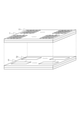
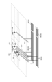
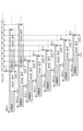
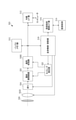
図1は、本実施例の撮像装置が備える、第1チップ1、第2チップ5を示した図である。第1チップ1と第2チップ5とは積層されている。第1チップ1には、複数行および複数列に渡って画素11が配されている。また、第2チップ5には、複数行および複数列に渡って、信号処理回路21が2次元状に配されている。なお、ここでは画素11と信号処理回路21のみを図示しているが、他に画素11を制御する制御線、画素11が出力する信号を伝送する信号線が適宜、第1チップ1に配される。また、垂直走査回路、タイミングジェネレータ等の駆動回路が適宜、第1チップ1あるいは第2チップ5に配される。
(Example 1)
(Overall configuration of the image pickup device)
FIG. 1 is a diagram showing a
(平面視における、画素と信号処理回路の配置関係)
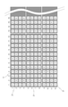
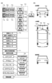
図2は、平面視における、第1チップ1が備える画素11と、第2チップ5が備える信号処理回路21のレイアウトを示した図である。図2では、画素11が備えるカラーフィルタの色も合わせて示している。図2に示したRは、画素11が赤(R)のカラーフィルタを備えることを示している。以下、同じくG、Bはそれぞれ、画素11が緑(G)、青(B)のカラーフィルタを備えることを示している。別の言い方をすれば、第1色に対応する波長の光が入射する画素と、第2色に対応する波長の光が入射する画素とを備えるとも言える。典型的には、赤色に対応する波長は600~830nmである。また、緑色に対応する波長は、500~600nmである。また、青色に対応する波長は360~500nmである。
(Arrangement relationship between pixels and signal processing circuit in plan view)
FIG. 2 is a diagram showing the layout of the
1つの信号処理回路21は、複数行および複数列に渡って配された画素11と重なるように配置されている。ここでは、1つの信号処理回路21は、4行12列の画素11に重なるように配置されている。後述するが、信号処理回路21は、マルチプレックス回路、増幅回路、アナログデジタル変換部を構成するアナログデジタル変換回路(以下、AD変換回路)を有する。したがって、1つの信号処理回路21のマルチプレックス回路と増幅回路とAD変換回路の一部、あるいは全部が、画素11に重なるように配置されていると言える。
One
また、後述するが、1つの信号処理回路21のAD変換回路は、第1色のカラーフィルタを備える画素11が出力する信号をAD変換し、第2色のカラーフィルタを備える画素11が出力する信号のAD変換を行わない。したがって、1つの信号処理回路21は、AD変換を行う対象の画素11と、AD変換を行わない対象の画素11との双方に対し、平面視において重なる関係となっている。
Further, as will be described later, the AD conversion circuit of one
なお、この配置は一例であって、本実施例では、1つの信号処理回路21に対し、複数の画素11が配されている形態を採用することができる。
Note that this arrangement is an example, and in this embodiment, it is possible to adopt a form in which a plurality of
(撮像装置の等価回路)
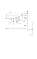
図3(a)では、図2に示した画素11のうち、奇数列の画素11のみを示している。第1チップ1の画素11は、1列の画素11に対し、4本の信号線201(A)~(D)を有する。なお、以下では信号線201(A)~(D)を区別なく表記する場合には、単に信号線201と表記する。1行目の画素11は信号線201(A)に接続されている。以下、同様に2~4行目の画素11は、順に信号線201(B)~(D)に接続されている。信号線201(A)~(D)は、他の列においても、1列目の画素11と同じように配されている。
(Equivalent circuit of image pickup device)
FIG. 3A shows only the odd-numbered
信号線201(A)、201(C)のそれぞれは、接続部303を介して、信号処理回路21(A)に接続されている。また、信号線201(B)、201(D)のそれぞれは、接続部303を介して、信号処理回路21(B)に接続されている。信号処理回路21(A)と信号処理回路21(B)とは、同じ回路構成を持つ。そのため、両者に共通する説明の場合は、アルファベットを省略する。以下、信号処理回路21の構成について説明する。
Each of the signal lines 201 (A) and 201 (C) is connected to the signal processing circuit 21 (A) via the
図3(b)は、信号処理回路21の等価回路を示す。複数の信号線201は、それぞれ、接続部303を介して信号処理回路21が備えるマルチプレックス回路(以下、MPX回路と表記する)350に接続されている。また、信号処理回路21は、増幅回路355、および、AD変換回路(以下、明細書および図面にてADCと表記する)360を有する。MPX回路350の出力は、増幅回路355を介して、ADC360に接続される。したがって、MPX回路350は、複数の信号線201の1つを選択して、ADC360(A)に接続する選択部である。本図では複数の信号線201の信号のうち1つを選択して1つの増幅回路355に出力する構成となっているが、実際は1つのMPX回路350に対して複数の増幅回路355が設けられた構成となっている。したがってMPX回路350は複数の入力ノードと複数の出力ノードとを有し、複数の入力ノードのいずれかに入力された画素からの信号を複数の出力ノードのいずれかに出力する構成となっている。
FIG. 3B shows an equivalent circuit of the
増幅回路355は、例えば、オペアンプである。増幅回路355は、反転入力端子と非反転入力端子とを備える。2つの入力端子の一方は、MPX回路350に接続される。2つの入力端子の他方には、参照電圧Vrefが供給される。図3の例では、参照電圧Vrefは容量を介して供給される。当該容量にはリセット用のスイッチが接続される。増幅回路355の2つの出力端子は、それぞれ、ADC360に接続される。また、増幅回路355の2つの出力端子は、それぞれ、反転入力端子および非反転入力端子に、フィードバック容量を介して接続される。各帰還経路において、フィードバック容量と並列に、初期化スイッチが接続される。増幅回路355は1より大きいゲインを有する。例えば、増幅回路355は、1倍と4倍のゲインを選択することができる。
The
図3に示しているように、ADC360(A)に接続される画素11は全て、Rのカラーフィルタを備える画素11である。一方、ADC360(B)に接続される画素11は全て、Gのカラーフィルタを備える画素11である。このように、各々が第1色(R)のカラーフィルタを備える複数の第1画素11は、第2AD変換部であるADC360(B)に接続されずに第1AD変換部であるADC360(A)に接続される。また、各々が第2色(G)のカラーフィルタを備える複数の第1画素11は、第1AD変換部であるADC360(A)に接続されずに第2AD変換部であるADC360(B)に接続される。
As shown in FIG. 3, all the
また、図3に示したように、第2チップ5は電流源310を有する。電流源310は、接続部303を介して、各列の信号線201に電流を供給する。
Further, as shown in FIG. 3, the
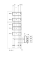
(撮像装置の接続部周りの断面構造)
図4は、図3に示した撮像装置の断面構造を示した図である。図4では、4行1列に配された画素11と、1行目11列目の画素11とを中心に記載している。図1に示した第1チップ1と第2チップ5は、接合面300で接合されている。
(Cross-sectional structure around the connection part of the image pickup device)
FIG. 4 is a diagram showing a cross-sectional structure of the image pickup apparatus shown in FIG. In FIG. 4, the
本実施例の撮像装置は、裏面照射型の撮像装置である。画素11は、不図示の光電変換部を備える。この光電変換部と、接合面300との間に信号線201が設けられている。信号線201は、画素11の所定の方向(図では列に沿った方向)に延在している。信号線201は、接続配線401を介して接続部303に接続される。また、MPX回路350(A)は、接続配線405を介して接続部303に接続される。接続配線401、接続配線405、接続部303は、平面視において重なるように配置されている。信号処理回路21と信号線201との接続は、接続配線405に対して、平面視において重なる位置に接続配線401を形成することによって行うことができるとも言える。そして、所定の方向に沿って延在する信号線201と接続配線401とを接続することによって、信号線201と、MPX回路350とを接続することができる。信号線201が所定の方向に延在していることにより、接続配線401と信号線201との接続を容易にすることができる。他の例として、図5に示すように、第1チップ1ではなく第2チップ5に、所定の方向に延在する信号線501を設けることが考えられる。この場合においても、画素11とMPX回路350(A)を接続することができる。しかしながら、図5に比べて、図4に示した、第1チップ1に、所定の方向に延在する信号線を設けることが好ましい。これは、画素11が備わる第1チップ1よりも、信号処理回路21が備わる第2チップ5の方が、配線層が多くなることに由来する。配線層の多い第2チップ5に、図5のように信号線501を設けるよりも、配線層の少ない第1チップ1に、図4のように信号線201を設ける方が、設計の自由度が高いためである。
The image pickup device of this embodiment is a back-illuminated image pickup device. The
(画素の等価回路)
図6は、本実施例の画素11の等価回路図である。画素11は、光電変換部であるフォトダイオード601a、601bを有する。フォトダイオード601a、601bには、不図示の1つのマイクロレンズと、図2に示した配列に従って設けられたカラーフィルタを透過した光が入射する。つまり、フォトダイオード601aに入射する光と、フォトダイオード601bに入射する光の波長は実質的に同じである。
(Pixel equivalent circuit)
FIG. 6 is an equivalent circuit diagram of the
フォトダイオード601aは、転送トランジスタ603aを介して、フローティングディフージョン部(以下、FD部)605に接続されている。また、転送トランジスタ603aのゲートは、制御線650を介して、不図示の垂直走査回路に接続されている。フォトダイオード601bは、転送トランジスタ603bを介して、FD部605に接続されている。また、転送トランジスタ603bのゲートは、制御線655を介して、不図示の垂直走査回路に接続されている。
The
FD部605は、リセットトランジスタ606と、増幅トランジスタ607のゲートに接続されている。
The
リセットトランジスタ606および増幅トランジスタ607は、電源電圧Vddが供給される。リセットトランジスタ606のゲートは、制御線660を介して、不図示の垂直走査回路に接続されている。
The power supply voltage Vdd is supplied to the
増幅トランジスタ607は、選択トランジスタ608に接続されている。選択トランジスタ608のゲートは、制御線665を介して、不図示の垂直走査回路に接続されている。
The
選択トランジスタ608は、信号線201に接続されている。
The
(撮像装置の動作)
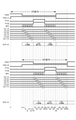
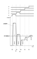
図7は、図6に示した画素11を備える撮像装置の動作を示した図である。
(Operation of image pickup device)
FIG. 7 is a diagram showing the operation of the image pickup apparatus including the
図7の信号PRESは、図6の制御線660を介して垂直走査回路からリセットトランジスタ606のゲートに供給される信号を示している。同じく、信号PSELは、制御線665を介して垂直走査回路からN行目の画素11の選択トランジスタ608のゲートに供給される信号を示している。なお、信号PSELについては、出力される画素11の行位置を末尾に合わせて示している。つまり、信号PSEL(1)は、1行目の画素11に出力される信号PSELであることを示している。信号PTXAは、制御線650を介して垂直走査回路から転送トランジスタ603aのゲートに供給される信号を示している。信号PTXBは、制御線655を介して垂直走査回路から転送トランジスタ603bのゲートに供給される信号を示している。
The signal PRESS of FIG. 7 shows a signal supplied from the vertical scanning circuit to the gate of the
図7では、MPX回路350(A)、ADC360(A)に関わる動作を示している。このMPX回路350(A)、ADC360(A)には、図3で示したように、Rのカラーフィルタを備える、1行目および3行目であって、1~12列のうちの奇数列に位置する画素11の信号が入力される。したがって、図7では、1行目、3行目であって、1~12列のうちの奇数列に位置する画素11の動作に関わる動作を示している。
FIG. 7 shows the operations related to the MPX circuits 350 (A) and ADC 360 (A). As shown in FIG. 3, the MPX circuits 350 (A) and ADC 360 (A) are provided with an R color filter in the first and third rows, and are odd columns among
また、図7に示した信号MPXは、不図示のタイミングジェネレータが、MPX回路350(A)に出力する信号を示している。信号MPXの信号値の変化によって、MPX回路350(A)は、増幅回路355(A)およびADC360(A)に出力する信号を、1~12列のうち、奇数列の画素11に対応する信号線201の中から順次変更する。以下では、MPX回路350が増幅回路355に信号を出力し、そして、増幅回路355が増幅された信号をADC360に出力することを、単に、MPX回路350がADC360に信号を出力するとも言う。
Further, the signal MPX shown in FIG. 7 indicates a signal output to the MPX circuit 350 (A) by a timing generator (not shown). Due to the change in the signal value of the signal MPX, the MPX circuit 350 (A) outputs the signal to the amplifier circuit 355 (A) and the ADC 360 (A) to the signal corresponding to the
図7では、MPX回路350(A)が、ADC360(A)に信号を出力する列としてどの列を選択しているかを、Col_nmとして示している。このnmの表記を説明する。nは画素11の列番号を示している。また、mは、1列の画素11に対応して配される信号線201(A)~(D)のアルファベットを示している。つまり、Col_1Aであれば、1列目の画素11に対応された信号線201(A)を示している。
In FIG. 7, which column is selected as the column for outputting the signal to the ADC 360 (A) by the MPX circuit 350 (A) is shown as Col_nm. The notation of this nm will be described. n indicates the column number of the
時刻t1において、垂直走査回路は、1行目および3行目の画素11に出力する信号PRESをHighレベルとしている。これにより、1行目の画素11のリセットトランジスタ606がオンしている。よって、FD部605は、電源電圧Vddに対応する電位にリセットされている。また、時刻t1において垂直走査回路は、信号PSEL(1)をHighレベルとしている。これにより、1行目の画素11の選択トランジスタ608がオンする。よって、図3に示した電流源310が供給する電流が、1行目の画素11の選択トランジスタ608を介して増幅トランジスタ607に供給される。これにより、電源電圧Vdd、増幅トランジスタ607、電流源310によるソースフォロワ回路が形成される。つまり、増幅トランジスタ607は、FD部605の電位に対応する信号を、選択トランジスタ608を介して信号線201に出力するソースフォロワ動作を行う。
At time t1, the vertical scanning circuit sets the signal PRESS to be output to the
(動作:1行目の画素11に対応するN信号の読み出し)
時刻t2に、垂直走査回路は、1行目の画素11に出力する信号PRESをLowレベルとする。これにより、1行目の画素11のリセットトランジスタ606がオフする。よって、FD部605のリセットが解除される。増幅トランジスタ607は、リセットが解除されたFD部605の電位に基づく信号を、図3に示した信号線201(A)に出力する。この信号を、N信号(ノイズ信号)と表記する。これにより、各列の信号線201(A)には、画素11からN信号が出力されている。
(Operation: Read N signal corresponding to
At time t2, the vertical scanning circuit sets the signal PRESS output to the
(動作:1行目の画素11に対応するN信号のAD変換)
時刻t2以降、MPX回路350(A)は、タイミングジェネレータから供給される信号MPXによって、1~12列のうち奇数列の画素11に対応する信号線201(A)を、順次ADC360(A)に接続する。
(Operation: AD conversion of N signal corresponding to
After time t2, the MPX circuit 350 (A) sequentially transfers the signal lines 201 (A) corresponding to the odd-numbered
ADC360(A)は、MPX回路350(A)から出力される、1列目の信号線201(A)のノイズ信号をデジタル信号にAD変換する。その後、順次、1~12列のうちの奇数列の画素11に対応する信号線201(A)に出力されているノイズ信号をデジタル信号にAD変換する。
The ADC 360 (A) AD-converts the noise signal of the signal line 201 (A) of the first row output from the MPX circuit 350 (A) into a digital signal. After that, the noise signal output to the signal line 201 (A) corresponding to the odd-numbered row of
(動作:3行目の画素11に対応するN信号の読み出し)
時刻t16に、垂直走査回路は、3行目の画素11に出力する信号をLowレベルとする。これにより、3行目の画素11のリセットトランジスタ606がオフする。よって、FD部605のリセットが解除される。増幅トランジスタ607は、リセットが解除されたFD部605の電位に基づく信号であるN信号を、図3に示した信号線201(C)に出力する。これにより、各列の信号線201(C)には、画素11からノイズ信号が出力されている。
(Operation: Read N signal corresponding to
At time t16, the vertical scanning circuit sets the signal output to the
(動作:3行目の画素11に対応するN信号のAD変換)
時刻t16以降、MPX回路350(A)は、タイミングジェネレータから供給される信号MPXによって、1~12列のうち奇数列の画素11に対応する信号線201(C)を、順次ADC360(A)に接続する。
(Operation: AD conversion of N signal corresponding to
After the time t16, the MPX circuit 350 (A) sequentially transfers the signal lines 201 (C) corresponding to the odd-numbered
ADC360(A)は、MPX回路350(A)から出力される、1列目の信号線201(C)のN信号をデジタル信号にAD変換する。その後、順次、1~12列のうちの奇数列の画素11に対応する信号線201(C)に出力されているN信号をデジタル信号にAD変換する。
The ADC 360 (A) AD-converts the N signal of the signal line 201 (C) of the first row output from the MPX circuit 350 (A) into a digital signal. After that, the N signal output to the signal line 201 (C) corresponding to the odd-numbered
(動作:1行目の画素11に対応するA+B信号の読み出し)
時刻t16に、垂直走査回路は、1行目の画素11に出力する信号PTXA、PTXBをHighレベルとする。これにより、フォトダイオード601a、601bが蓄積した電荷(本実施例では電子である)が、転送トランジスタ603a、603bを介してFD部605に転送される。FD部605では、フォトダイオード601a、601bのそれぞれの電荷が加算される。これにより、FD部605は、フォトダイオード601a、601bのそれぞれの電荷を加算した電荷に対応する電位となる。仮に、フォトダイオード601aのみの電荷によるFD部605の電位に基づいて増幅トランジスタ607が出力する信号をA信号とする。また、仮に、フォトダイオード601bのみの電荷によるFD部605の電位に基づいて増幅トランジスタ607が出力する信号をB信号とする。この表記に従うと、フォトダイオード601a、601bのそれぞれの電荷を加算した電荷に対応するFD部605の電位に基づいて増幅トランジスタ607が出力する信号はA信号とB信号を加算したA+B信号とみなすことができる。各列の信号線201(A)には、1行目の画素11のA+B信号が出力されている。
(Operation: Read A + B signal corresponding to
At time t16, the vertical scanning circuit sets the signals PTXA and PTXB output to the
(1行目の画素11に対応するA+B信号のAD変換)
時刻t30以降、MPX回路350(A)は、タイミングジェネレータから供給される信号MPXによって、1~12列のうち奇数列の画素11に対応する信号線201(A)を、順次ADC360(A)に接続する。
(AD conversion of A + B signal corresponding to
After the time t30, the MPX circuit 350 (A) sequentially transfers the signal lines 201 (A) corresponding to the odd-numbered
ADC360(A)は、MPX回路350(A)から出力される、1列目の信号線201(A)のA+B信号をデジタル信号にAD変換する。その後、順次、1~12列のうちの奇数列の画素11に対応する信号線201(A)に出力されているA+B信号をデジタル信号にAD変換する。
The ADC 360 (A) AD-converts the A + B signal of the signal line 201 (A) of the first row output from the MPX circuit 350 (A) into a digital signal. After that, the A + B signal output to the signal line 201 (A) corresponding to the odd-numbered
(動作:3行目の画素11に対応するA+B信号の読み出し)
時刻t30に、垂直走査回路は、3行目の画素11に出力する信号PTXA、PTXBをHighレベルとする。これにより、各列の信号線201(C)には、3行目の画素11のA+B信号が出力されている。
(Operation: Read A + B signal corresponding to
At time t30, the vertical scanning circuit sets the signals PTXA and PTXB output to the
(動作:3行目の画素11に対応するA+B信号のAD変換)
時刻t44以降、MPX回路350(A)は、タイミングジェネレータから供給される信号MPXによって、1~12列のうち奇数列の画素11に対応する信号線201(C)を、順次ADC360(A)に接続する。
(Operation: AD conversion of A + B signal corresponding to
After the time t44, the MPX circuit 350 (A) sequentially transfers the signal lines 201 (C) corresponding to the odd-numbered
ADC360(A)は、MPX回路350(A)から出力される、1列目の信号線201(C)のA+B信号をデジタル信号にAD変換する。その後、順次、1~12列のうちの奇数列の画素11に対応する信号線201(C)に出力されているA+B信号をデジタル信号にAD変換する。
The ADC 360 (A) AD-converts the A + B signal of the signal line 201 (C) of the first row output from the MPX circuit 350 (A) into a digital signal. After that, the A + B signal output to the signal line 201 (C) corresponding to the odd-numbered
(撮像装置が行う並行動作)
図7に示した動作では、以下のように、複数の動作を並行して行っている。
(1)1行目の画素11に対応するN信号のAD変換と、3行目の画素11に対応するN信号の読み出しとの並行動作
(2)3行目の画素11に対応するN信号のAD変換と、1行目の画素11に対応するA+B信号の読み出しとの並行動作
(3)1行目の画素11に対応するA+B信号のAD変換と、3行目の画素11に対応するA+B信号の読み出しとの並行動作
この並行動作により、ADC360(A)が1度のAD変換を終えてから、次のAD変換を行うまでの待機期間を短縮することができる。これにより、全ての画素11が出力する信号のAD変換に要する期間を短縮することができる。よって、撮像装置の高フレームレート化を進展させることができる。
(Parallel operation performed by the image pickup device)
In the operation shown in FIG. 7, a plurality of operations are performed in parallel as follows.
(1) Parallel operation of AD conversion of the N signal corresponding to the
(本実施例の効果)
本実施例の撮像装置では、信号処理回路21が増幅回路355を含む。そのため、ADC360で生じるノイズが重畳される前に、信号が増幅される。結果として、SN比を向上させることができる。
(Effect of this example)
In the image pickup apparatus of this embodiment, the
(他の形態)
本実施例では、第1色のカラーフィルタが配された画素11が接続され、第2色のカラーフィルタが配された画素11が接続されていない信号線201が、ADC360に接続される例を説明した。この例では、当該ADC360と第2色のカラーフィルタが配された画素11とが接続される接続部が設けられない形態となる。
(Other forms)
In this embodiment, the
本実施例は、この例に限定されるものでは無い。例えば、図8に示したように、1列の画素11に対し、複数の信号線が配され、この複数の信号線がMPX回路350によって、選択的にADC360に接続される例にも適用することが可能である。この例の場合には、異なる色のカラーフィルタを備える複数の画素11が、1つの信号処理回路21に接続される。この構成においても、上記したSN比向上の効果を得ることができる。
The present embodiment is not limited to this example. For example, as shown in FIG. 8, a plurality of signal lines are arranged for one row of
(実施例2)
本実施例について、実施例1と異なる点を中心に説明する。本実施例の撮像装置においては、信号処理回路21の構成が、実施例1の信号処理回路21と異なる。具体的に、本実施例の信号処理回路21は、2つのマルチプレックス回路と、その間に並列に配置された複数の増幅回路を備える。その他の構成は、実施例1の撮像装置の構成と同じとすることができる。以下、実施例1と異なる点を中心に説明する。
(Example 2)
This embodiment will be described focusing on the differences from the first embodiment. In the image pickup apparatus of this embodiment, the configuration of the
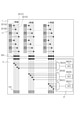
図9は、本実施例の撮像装置の信号処理回路21の等価回路を示している。信号処理回路21が、MPX回路350とADC360とを含む点は、実施例1と同様である。なお、図9では、MPX回路350の入力に、符号sf1~sf8が付されている。図9では、MPX回路350の8入力であるが、入力の数は特に限定されない。
FIG. 9 shows an equivalent circuit of the
MPX回路350は4つの出力ノードを備える。MPX回路350の各出力ノードには、増幅回路355が接続される。信号処理回路21は、4つの増幅回路355a~355dを備える。MPX回路350は、入力sf1と入力sf5のいずれかを選択し、選択された入力信号を増幅回路355aに出力する。また、MPX回路350は、入力sf2と入力sf5のいずれかを選択し、選択された入力信号を増幅回路355bに出力する。他の入力についても同様である。各増幅回路355の反転入力端子および非反転端子の一方には、MPX350から出力された信号が容量を介して入力される。各増幅回路355の反転入力端子および非反転端子の他方には、参照信号Vrefが入力される。複数の増幅回路355に、共通の参照信号Vrefが供給されうる。
The
複数の増幅回路355の出力は、共通のマルチプレックス回路356(以下、MPX回路356)に接続される。MPX回路356は、複数の増幅回路355の出力の1つを選択肢、選択された信号をADC360に出力する。MPX回路356は、複数の増幅回路355の反転出力端子からの信号の中から1つの信号を選択する。また、MPX回路356は、複数の増幅回路355の非反転出力端子からの信号の中から1つの信号を選択する。
The outputs of the plurality of
なお、図9が示すとおり、MPX回路350への入力の数より、MPX回路356への入力の数が少ない。また、MPX回路350への入力の数より、複数の増幅回路355の数が少ない。
As shown in FIG. 9, the number of inputs to the
このように、本実施例では、2つの選択回路(MPX回路350およびMPX回路356)の間に、複数の増幅回路355が並列に接続される。このような構成により、信号出力の高速化が可能である。
As described above, in this embodiment, a plurality of
図10を用いて本実施例の信号処理回路21の動作を説明する。図10は、出力線201ごとの信号に対する処理動作を模式的に示している。
The operation of the
入力sf1に接続された出力線201の信号の処理について説明する。まず信号φSEL1がオンすることで、画素11のソースフォロア回路から、入力sf1に接続された出力線201へ、画素信号が出力される。そのごMUX1のタイミングで、MPX回路355aは、入力sf1を選択し、そして、入力sf1の信号を後段の増幅回路355aに出力する。増幅回路355aの出力が安定した時点(MUX2)で、MPX回路356が増幅回路355aの出力を後段のADC360に出力する。ADC360は、増幅回路355aによって増幅された画素信号に対してAD変換を行う。図10は、N信号のAD変換を例に示している。
The processing of the signal of the
信号φSEL1がオンしてから所定の時間が経過した後、信号φSEL5がオンする。これにより、画素11のソースフォロア回路から、入力sf5に接続された出力線201へ、画素信号が出力される。その後MUX1のタイミングで、MPX回路350は、入力sf5を選択し、そして、入力sf5の信号を後段の増幅回路355aに出力する。このように1つの増幅回路355にある信号が入力されたから次の信号が入力されるまでには、当該増幅回路355の前の信号の出力が安定するまでの期間が経過する。
After a predetermined time has elapsed since the signal φSEL1 was turned on, the signal φSEL5 is turned on. As a result, the pixel signal is output from the source follower circuit of the
ここで本実施例では、MPX回路350の後段に複数の増幅回路355が並列に接続されている。そのため、1つの増幅回路355の前の信号の出力が安定するまでの期間に、他の増幅回路355に信号を入力することができる。具体的には、信号φSEL1がオンしてから信号φSEL5がオンするまでの間に、信号φSEL2~4がオンしている。これにより、MPX回路350は、入力sf2~sf4の信号を順次、増幅回路355b~355dへ出力している。結果として複数の信号を出力する動作を高速化することが可能である。
Here, in this embodiment, a plurality of
図10が示すとおり、1つのMPX回路350に接続された複数の画素11において、選択トランジスタを制御する信号φSEL1~8が順次オンする。信号φSEL1~8がオンする間隔に対して、MPX回路350が1つの出力を切り替える間隔が長い。たとえば、信号φSEL1がオンしてから信号φSEL2がオンするまでの間隔より、入力sf1に対するタイミングMUX1と入力sf5に対するタイミングMUX1との間隔のほうが長い。これにより、画素信号の伝達経路にある各回路の出力が十分に安定する時間が確保される。
As shown in FIG. 10, in the plurality of
また、別の観点では、増幅回路355の後段に選択回路(MPX回路356)が配される。これにより、選択回路で生じるノイズの影響を低減することが可能である。結果として、画質を向上させることができる。
From another viewpoint, a selection circuit (MPX circuit 356) is arranged after the
続いて、本実施例の変形例を説明する。図11は、撮像装置の画素と信号処理回路の接続を示す図である。図11の撮像装置は、参照信号Vrefを出力するダミー画素12を有する。各ダミー画素は出力線dummyに接続される。出力線dummyには電流源が接続されている。ダミー画素12は、画素11と同様に増幅トランジスタ607を含む。そのため、増幅トランジスタ607と出力線dummyに接続された電流源とがソースフォロア回路を構成する。ダミー画素12には、光電変換部の代わりに基準電圧を供給する電圧供給部が配される。このような構成により、ダミー画素12は参照電圧Vrefを出力することができる。
Subsequently, a modified example of this embodiment will be described. FIG. 11 is a diagram showing the connection between the pixels of the image pickup apparatus and the signal processing circuit. The image pickup apparatus of FIG. 11 has a
ダミー画素12が参照電圧Vrefを出力する事で、複数の出力線201の間に発生するクロストークを打ち消すことができる。また、複数の列にダミー画素12を配置し、かつ、複数の列にダミー画素12の出力を互いにショートする事で、参照信号Vrefに重畳されるトランジスタ起因のノイズを平均化する事が可能である。結果として、画質を向上させることが可能である。
By outputting the reference voltage Vref by the
(実施例3)
本実施例について、実施例1と異なる点を中心に説明する。本実施例の撮像装置は、実施例1および実施例2のADC360として、逐次比較型のAD変換器を用いた例である。その他の構成は、実施例1または実施例2の撮像装置の構成と同じとすることができる。
(Example 3)
This embodiment will be described focusing on the differences from the first embodiment. The image pickup apparatus of this example is an example in which a successive approximation type AD converter is used as the
(逐次比較型ADCの等価回路)
図12は、本実施例のADC360の等価回路図である。
(Equivalent circuit of successive approximation type ADC)
FIG. 12 is an equivalent circuit diagram of the
ADC360は入力端子IN及び出力端子OUTを有し、入力端子INから入力されたアナログ信号Sin(MPX回路350の出力)をデジタル信号Soutに変換して出力端子OUTから出力する。このアナログ信号Sinは、実施例1で説明した、N信号とS信号の一方あるいは両王とすることができる。ADC360はMPX回路出力を5ビットの分解能でデジタル信号Soutに変換する。
The
ADC360はアナログ信号Sinとの比較に用いられる比較信号を生成する生成回路810を更に有する。生成回路810はバイナリウェイトの容量値を有する複数の容量素子cp0~cp4と、容量素子cp0~cp4に接続された複数のスイッチsw0~sw4とを有する。複数のスイッチsw0~sw4によって、容量素子cp0~cp4のうちの1つ以上を選択するスイッチ回路が構成される。バイナリウェイトとは、公比2の等比数列をなす重み(容量値)の集合のことである。図12の例では、容量素子cp0~cp4は順に、1C、2C、4C、8C、16Cの容量値を有する。容量素子cp0~cp4の一方の電極は生成回路810の供給端子SPLに接続され、他方の電極はそれぞれスイッチsw0~sw4に接続される。スイッチsw0~sw4はそれぞれ、一端が容量素子cp0~cp4に接続され、他端が端子Aと端子Bとの間をトグルする。端子Aには接地電位GNDが供給され、端子Bには基準電圧VRFが供給される。基準電圧VRFはADC360の外部から供給される定電圧であり、接地電位GNDよりも大きな値である。スイッチsw0が端子Aにトグルすると、容量素子cp0に接地電位GNDが供給され、スイッチsw0が端子Bにトグルすると、容量素子cp0に基準電圧VRFが供給される。他のスイッチsw1~sw4についても同様である。スイッチsw0~sw4が切り替わることによって、供給端子SPLと基準電圧VRFとの間に接続される容量素子の合成容量値が変化し、その結果として供給端子SPLから出力される比較信号Vcmpの値が変化する。
The
ADC360は比較器815を更に有する。比較器815はアナログ信号Sinの値と比較信号Vcmpの値とを比較して、比較結果に応じた信号を出力する。比較器815の非反転端子には容量素子cp6を介してアナログ信号Sinが供給され、比較器815の反転端子には生成回路810の供給端子SPLから比較信号Vcmpが供給される。それにより、アナログ信号Sinの値が比較信号Vcmpの値以上の場合にHighが出力され、アナログ信号Sinの値が比較信号Vcmpの値未満の場合にLowが出力される。この例ではアナログ信号Sinの値と比較信号Vcmpの値が等しい場合にHighを出力しているが、Lowを出力してもよい。容量素子cp6はアナログ信号Sinの値を比較信号Vcmpとの比較が可能な範囲に調整する。本実施形態では、説明を簡単にするために、アナログ信号Sinの値は接地電位GND以上、基準電圧VRF以下であり、アナログ信号Sinと同じ大きさの信号が比較器815の非反転端子に供給される場合を扱う。
The
図12の例ではアナログ信号Sinを比較器815の非反転端子に供給し、比較信号Vcmpを比較器815の反転端子に供給するが、アナログ信号Sinの値と比較信号Vcmpの値との大小関係を判定できれば他の構成も取りうる。例えば、アナログ信号Sinと比較信号Vcmpとの差分を比較器815の非反転端子に供給し、接地電位GNDを比較器815の反転端子に供給してもよい。
In the example of FIG. 12, the analog signal Sin is supplied to the non-inverting terminal of the
ADC360はスイッチsw5、sw6を更に有する。これらのスイッチsw5、sw6が導通状態になると、比較器815の非反転端子、反転端子に接地電位GNDが供給され、比較器815がリセットされる。
The
ADC360は、制御回路820を更に備える。制御回路820には比較器815から比較結果が供給され、制御回路820はこの比較結果に基づいてデジタル信号Soutを生成し、出力端子OUTから出力する。制御回路820はまた、各スイッチsw0~sw6に制御信号を送信してその状態を切り替える。
The
(逐次比較型ADCの動作)
図13において、sw0~sw6は制御回路820からスイッチsw0~sw6に供給される制御信号の値を示す。スイッチsw0~sw4は、供給される制御信号がHighである場合に端子Bへトグルし、制御信号がLowである場合に端子Aへトグルする。スイッチsw5、sw6は、供給される制御信号がHighである場合に導通状態となり、制御信号がLowである場合に非導通状態となる。図13の下側にはアナログ信号Sin及び比較信号Vcmpが示される。図13では、アナログ信号Sinの値が2進数で00110に相当する場合を例として扱う。
(Operation of successive approximation type ADC)
In FIG. 13, sw0 to sw6 indicate the values of the control signals supplied from the
続いて、AD変換器100のAD変換動作を時系列に沿って説明する。制御回路820は準備期間において、スイッチsw0~sw4に供給される制御信号をLowにし、スイッチsw5、sw6に供給される制御信号をHighにする。これにより、比較器815の非反転端子及び反転端子が接地電位GNDにリセットされるとともに、比較信号Vcmpの値が接地電位GNDに等しくなる。その後、制御回路820はスイッチsw5、sw6に供給される制御信号をLowにする。以降の動作において、比較器815の非反転端子にはアナログ信号Sinが供給され続ける。
Subsequently, the AD conversion operation of the AD converter 100 will be described in chronological order. During the preparation period, the
次に、逐次比較期間が始まると、制御回路820はスイッチsw4に供給される制御信号をHighに変更する。これにより、スイッチsw4は端子Bにトグルし、バイナリウェイトの中で1番目に大きな容量値を有するキャパシタcp4を介して生成回路810の供給端子SPLに基準電圧VRFが印加される。その結果、比較信号VcmpがVRF/2だけ増加し、比較信号Vcmpの値はVRF/2に等しくなる。制御回路820は、比較器815からの比較結果に基づいて、アナログ信号Sinの値が比較信号Vcmpの値(VRF/2)よりも小さいと判定し、スイッチsw4に供給される制御信号をLowに戻す。それにより、比較信号Vcmpの値は接地電位GNDに戻る。この比較結果は、デジタル信号Soutの値のMSB(LSBを1ビット目とした場合に5ビット目)が0であることを意味する。
Next, when the sequential comparison period starts, the
次に、制御回路820はスイッチsw3に供給される制御信号をHighに変更する。これにより、バイナリウェイトの中で2番目に大きな容量値を有するキャパシタcp3を介して生成回路810の供給端子SPLに基準電圧VRFが印加される。その結果、比較信号VcmpがVRF/4だけ増加し、比較信号Vcmpの値はVRF/4に等しくなる。制御回路820は、比較器815からの比較結果に基づいて、アナログ信号Sinの値が比較信号Vcmpの値(VRF/4)よりも小さいと判定し、スイッチsw3に供給される制御信号をLowに戻す。それにより、比較信号Vcmpの値は接地電位GNDに戻る。この比較結果は、デジタル信号Soutの値の4ビット目が0であることを意味する。
Next, the
次に、制御回路820はスイッチsw2に供給される制御信号をHighに変更する。これにより、バイナリウェイトの中で3番目に大きな容量値を有するキャパシタcp2を介して生成回路810の供給端子SPLに基準電圧VRFが印加される。その結果、比較信号VcmpがVRF/8だけ増加し、比較信号Vcmpの値はVRF/8に等しくなる。制御回路820は、比較器815からの比較結果に基づいて、アナログ信号Sinの値が比較信号Vcmpの値(VRF/8)よりも大きいと判定し、スイッチsw2に供給される制御信号をHighのままにする。それにより、比較信号Vcmpの値はVRF/8に維持される。この比較結果は、デジタル信号Soutの値の3ビット目が1であることを意味する。
Next, the
次に、制御回路820はスイッチsw1に供給される制御信号をHighに変更する。これにより、バイナリウェイトの中で4番目に大きな容量値を有するキャパシタcp1と、キャパシタcp2とを介して生成回路810の供給端子SPLに基準電圧VRFが印加される。その結果、比較信号VcmpがVRF/16だけ増加し、比較信号Vcmpの値はVRF*3/16に等しくなる。なお、本明細書で用いる「*」は乗算を意味している。制御回路820は、比較器815からの比較結果に基づいて、アナログ信号Sinの値が比較信号Vcmpの値(VRF*3/16)よりも大きいと判定し、スイッチsw1に供給される制御信号をHighのままにする。それにより、比較信号Vcmpの値はVRF*3/16に維持される。この比較結果は、デジタル信号Soutの値の2ビット目が1であることを意味する。
Next, the
最後に、制御回路820はスイッチsw0に供給される制御信号をHighに変更する。これにより、バイナリウェイトの中で5番目に大きな容量値を有するキャパシタcp0と、cp1、cp2とを介して生成回路810の供給端子SPLに基準電圧VRFが印加される。その結果、比較信号VcmpがVRF/32だけ増加し、比較信号Vcmpの値はVRF*7/32に等しくなる。制御回路820は、比較器815からの比較結果に基づいて、アナログ信号Sinの値が比較信号Vcmpの値(VRF*7/32)よりも小さいと判定し、スイッチsw0に供給される制御信号をLowに戻す。それにより、比較信号Vcmpの値はVRF*3/16に戻る。この比較結果は、デジタル信号Soutの値の1ビット目が0であることを意味する。
Finally, the
以上の逐次比較により、制御回路820はアナログ信号に対応するデジタル信号Soutが00110であると決定する。
By the above sequential comparison, the
このようにして、ADC360は、入力されるアナログ信号に対応するデジタル信号を生成するAD変換を行うことができる。
In this way, the
(他のAD変換形式)
実施例2では、ADC360として、逐次比較型のAD変換器を用いた例を説明した。ADC360は、この逐次比較型のAD変換器に限定されるものでは無い。例えば、他のAD変換器として、ランプ信号比較型、デルタシグマ型、パイプライン型、フラッシュ型等の種々のAD変換器を用いることができる。
(Other AD conversion formats)
In Example 2, an example in which a successive approximation type AD converter is used as the
(実施例4)
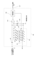
図14は、本実施例による撮像システム500の構成を示すブロック図である。本実施例の撮像システム500は、上述の各実施例で述べた撮像装置のいずれかの構成を適用した撮像装置200を含む。撮像システム500の具体例としては、デジタルスチルカメラ、デジタルカムコーダー、監視カメラ等が挙げられる。図14に、上述の各実施例のいずれかの撮像装置を撮像装置200として適用したデジタルスチルカメラの構成例を示す。
(Example 4)
FIG. 14 is a block diagram showing the configuration of the
図14に例示した撮像システム500は、撮像装置200、被写体の光学像を撮像装置200に結像させるレンズ5020、レンズ5020を通過する光量を可変にするための絞り504、レンズ5020の保護のためのバリア506を有する。レンズ5020及び絞り504は、撮像装置200に光を集光する光学系である。
The
撮像システム500は、また、撮像装置200から出力される出力信号の処理を行う信号処理部5080を有する。信号処理部5080は、必要に応じて入力信号に対して各種の補正、圧縮を行って出力する信号処理の動作を行う。信号処理部5080は、撮像装置200より出力される出力信号に対してAD変換処理を実施する機能を備えていてもよい。この場合、撮像装置200の内部には、必ずしもAD変換回路を有する必要はない。
The
撮像システム500は、更に、画像データを一時的に記憶するためのバッファメモリ部510、外部コンピュータ等と通信するための外部インターフェース部(外部I/F部)512を有する。更に撮像システム500は、撮像データの記録又は読み出しを行うための半導体メモリ等の記録媒体514、記録媒体514に記録又は読み出しを行うための記録媒体制御インターフェース部(記録媒体制御I/F部)516を有する。なお、記録媒体514は、撮像システム500に内蔵されていてもよく、着脱可能であってもよい。
The
更に撮像システム500は、各種演算を行うとともにデジタルスチルカメラ全体を制御する全体制御・演算部518、撮像装置200と信号処理部5080に各種タイミング信号を出力するタイミング発生部520を有する。ここで、タイミング信号などは外部から入力されてもよく、撮像システム500は、少なくとも撮像装置200と、撮像装置200から出力された出力信号を処理する信号処理部5080とを有すればよい。全体制御・演算部518及びタイミング発生部520は、撮像装置200の制御機能の一部又は全部を実施するように構成してもよい。
Further, the
撮像装置200は、画像用信号を信号処理部5080に出力する。信号処理部5080は、撮像装置200から出力される画像用信号に対して所定の信号処理を実施し、画像データを出力する。また、信号処理部5080は、画像用信号を用いて、画像を生成する。
The
上述した各実施例の撮像装置による撮像装置を用いて撮像システムを構成することにより、より良質の画像が取得可能な撮像システムを実現することができる。 By configuring the image pickup system by using the image pickup device by the image pickup device of each of the above-described embodiments, it is possible to realize an image pickup system capable of acquiring a higher quality image.
(実施例5)
本実施例の撮像システム及び移動体について、図15及び図16を用いて説明する。
(Example 5)
The imaging system and the moving body of this embodiment will be described with reference to FIGS. 15 and 16.
図15は、本実施例による撮像システム及び移動体の構成例を示す概略図である。図16は、本実施例による撮像システムの動作を示すフロー図である。 FIG. 15 is a schematic view showing a configuration example of an imaging system and a moving body according to this embodiment. FIG. 16 is a flow chart showing the operation of the imaging system according to this embodiment.
本実施例では、車載カメラに関する撮像システムの一例を示す。図15は、車両システムとこれに搭載される撮像システムの一例を示したものである。撮像システム701は、撮像装置702、画像前処理部715、集積回路703、光学系714を含む。光学系714は、撮像装置702に被写体の光学像を結像する。撮像装置702は、光学系714により結像された被写体の光学像を電気信号に変換する。撮像装置702は、上述の各実施例のいずれかの撮像装置である。画像前処理部715は、撮像装置702から出力された信号に対して所定の信号処理を行う。画像前処理部715の機能は、撮像装置702内に組み込まれていてもよい。撮像システム701には、光学系714、撮像装置702及び画像前処理部715が、少なくとも2組設けられており、各組の画像前処理部715からの出力が集積回路703に入力されるようになっている。
In this embodiment, an example of an imaging system related to an in-vehicle camera is shown. FIG. 15 shows an example of a vehicle system and an imaging system mounted on the vehicle system. The
集積回路703は、撮像システム用途向けの集積回路であり、メモリ705を含む画像処理部704、光学測距部706、視差演算部707、物体認知部708、異常検出部709を含む。画像処理部704は、画像前処理部715の出力信号に対して、現像処理や欠陥補正等の画像処理を行う。メモリ705は、撮像画像の一次記憶、撮像画素の欠陥位置を格納する。光学測距部706は、被写体の合焦や、測距を行う。視差演算部707は、複数の撮像装置702により取得された複数の画像データから視差(視差画像の位相差)の算出を行う。物体認知部708は、車、道、標識、人等の被写体の認知を行う。異常検出部709は、撮像装置702の異常を検出すると、主制御部713に異常を発報する。
The
集積回路703は、専用に設計されたハードウェアによって実現されてもよいし、ソフトウェアモジュールによって実現されてもよいし、これらの組合せによって実現されてもよい。また、FPGA(Field Programmable Gate Array)やASIC(Application Specific Integrated Circuit)等によって実現されてもよいし、これらの組合せによって実現されてもよい。
The
主制御部713は、撮像システム701、車両センサ710、制御ユニット720等の動作を統括・制御する。なお、主制御部713を持たず、撮像システム701、車両センサ710、制御ユニット720が個別に通信インターフェースを有して、それぞれが通信ネットワークを介して制御信号の送受を行う(例えばCAN規格)方法も取りうる。
The
集積回路703は、主制御部713からの制御信号を受け或いは自身の制御部によって、撮像装置702へ制御信号や設定値を送信する機能を有する。例えば、集積回路703は、撮像装置702内の電圧スイッチ13をパルス駆動させるための設定や、フレーム毎に電圧スイッチ13を切り替える設定等を送信する。
The
撮像システム701は、車両センサ710に接続されており、車速、ヨーレート、舵角などの自車両走行状態及び自車外環境や他車・障害物の状態を検出することができる。車両センサ710は、視差画像から対象物までの距離情報を取得する距離情報取得手段でもある。また、撮像システム701は、自動操舵、自動巡行、衝突防止機能等の種々の運転支援を行う運転支援制御部711に接続されている。特に、衝突判定機能に関しては、撮像システム701や車両センサ710の検出結果を基に他車・障害物との衝突推定・衝突有無を判定する。これにより、衝突が推定される場合の回避制御、衝突時の安全装置起動を行う。
The
また、撮像システム701は、衝突判定部での判定結果に基づいて、ドライバーに警報を発する警報装置712にも接続されている。例えば、衝突判定部の判定結果として衝突可能性が高い場合、主制御部713は、ブレーキをかける、アクセルを戻す、エンジン出力を抑制するなどして、衝突を回避、被害を軽減する車両制御を行う。警報装置712は、音等の警報を鳴らす、カーナビゲーションシステムやメーターパネルなどの表示部画面に警報情報を表示する、シートベルトやステアリングに振動を与えるなどしてユーザに警告を行う。
The
本実施例では、車両の周囲、例えば前方又は後方を撮像システム701で撮影する。図15(b)に、車両前方を撮像システム701で撮像する場合の撮像システム701の配置例を示す。
In this embodiment, the surroundings of the vehicle, for example, the front or the rear, are photographed by the
2つの撮像装置702は、車両700の前方に配置される。具体的には、車両700の進退方位又は外形(例えば車幅)に対する中心線を対称軸に見立て、その対称軸に対して2つの撮像装置702が線対称に配置されると、車両700と被写対象物との間の距離情報の取得や衝突可能性の判定を行う上で好ましい。また、撮像装置702は、運転者が運転席から車両700の外の状況を視認する際に運転者の視野を妨げない配置が好ましい。警報装置712は、運転者の視野に入りやすい配置が好ましい。
The two
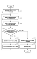
次に、撮像システム701における撮像装置702の故障検出動作について、図16を用いて説明する。撮像装置702の故障検出動作は、図16に示すステップS810~S880に従って実施される。
Next, the failure detection operation of the
ステップS810は、撮像装置702のスタートアップ時の設定を行うステップである。すなわち、撮像システム701の外部(例えば主制御部713)又は撮像システム701の内部から、撮像装置702の動作のための設定を送信し、撮像装置702の撮像動作及び故障検出動作を開始する。
Step S810 is a step for setting the start-up of the
次いで、ステップS820において、有効画素から画素信号を取得する。また、ステップS830において、故障検出用に設けた故障検出画素からの出力値を取得する。この故障検出画素は、有効画素と同じく光電変換部を備える。この光電変換部には、所定の電圧が書き込まれる。故障検出用画素は、この光電変換部に書き込まれた電圧に対応する信号を出力する。なお、ステップS820とステップS830とは逆でもよい。 Next, in step S820, a pixel signal is acquired from the effective pixel. Further, in step S830, the output value from the failure detection pixel provided for failure detection is acquired. The failure detection pixel includes a photoelectric conversion unit like the effective pixel. A predetermined voltage is written in this photoelectric conversion unit. The failure detection pixel outputs a signal corresponding to the voltage written in the photoelectric conversion unit. The steps S820 and S830 may be reversed.
次いで、ステップS840において、故障検出画素の出力期待値と、実際の故障検出画素からの出力値との該非判定を行う。 Next, in step S840, the non-determination of the expected output value of the failure detection pixel and the output value from the actual failure detection pixel is performed.
ステップS840における該非判定の結果、出力期待値と実際の出力値とが一致している場合は、ステップS850に移行し、撮像動作が正常に行われていると判定し、処理ステップがステップS860へと移行する。ステップS860では、走査行の画素信号をメモリ705に送信して一次保存する。そののち、ステップS820に戻り、故障検出動作を継続する。
If the expected output value and the actual output value match as a result of the non-determination in step S840, the process proceeds to step S850, it is determined that the imaging operation is normally performed, and the processing step proceeds to step S860. And migrate. In step S860, the pixel signal of the scanning line is transmitted to the
一方、ステップS840における該非判定の結果、出力期待値と実際の出力値とが一致していない場合は、処理ステップはステップS870に移行する。ステップS870において、撮像動作に異常があると判定し、主制御部713、又は警報装置712に警報を発報する。警報装置712は、表示部に異常が検出されたことを表示させる。その後、ステップS880において撮像装置702を停止し、撮像システム701の動作を終了する。
On the other hand, if the expected output value and the actual output value do not match as a result of the non-determination in step S840, the processing step proceeds to step S870. In step S870, it is determined that there is an abnormality in the imaging operation, and an alarm is issued to the
なお、本実施例では、1行毎にフローチャートをループさせる例を例示したが、複数行毎にフローチャートをループさせてもよいし、1フレーム毎に故障検出動作を行ってもよい。 In this embodiment, an example in which the flowchart is looped for each line is illustrated, but the flowchart may be looped for each of a plurality of lines, or the failure detection operation may be performed for each frame.
なお、ステップS870の警報の発報は、無線ネットワークを介して、車両の外部に通知するようにしてもよい。 The alarm in step S870 may be notified to the outside of the vehicle via the wireless network.
また、本実施例では、他の車両と衝突しない制御を説明したが、他の車両に追従して自動運転する制御や、車線からはみ出さないように自動運転する制御などにも適用可能である。さらに、撮像システム701は、自車両等の車両に限らず、例えば、船舶、航空機或いは産業用ロボットなどの移動体(移動装置)に適用することができる。加えて、移動体に限らず、高度道路交通システム(ITS)等、広く物体認識を利用する機器に適用することができる。
Further, in this embodiment, the control that does not collide with other vehicles has been described, but it can also be applied to the control that automatically drives following other vehicles and the control that automatically drives so as not to go out of the lane. .. Further, the
[変形実施例]
本発明は、上記実施例に限らず種々の変形が可能である。
[Modification Example]
The present invention is not limited to the above embodiment, and various modifications are possible.
例えば、いずれかの実施例の一部の構成を他の実施例に追加した例や、他の実施例の一部の構成と置換した例も、本発明の実施例である。 For example, an example in which a partial configuration of any of the examples is added to another embodiment or an example in which a partial configuration of another embodiment is replaced is also an example of the present invention.
また、上述の実施例は、いずれも本発明を実施するにあたっての具体化の例を示したものに過ぎず、これらの例示によって本発明の技術的範囲が限定的に解釈されてはならない。すなわち、本発明はその技術思想、又はその主要な特徴から逸脱することなく、様々な態様で実施することができる。 In addition, the above-mentioned examples are merely examples of embodiment in carrying out the present invention, and the technical scope of the present invention should not be construed in a limited manner by these examples. That is, the present invention can be carried out in various embodiments without departing from the technical idea or its main features.
1 第1チップ
5 第2チップ
11 画素
21 信号処理回路
303 接続部
310 電流源
703 マルチプレックス回路(MPX回路)
704 AD変換回路(ADC)
1
704 AD conversion circuit (ADC)
Claims (13)
前記第1チップに積層され、2次元状に配された複数の信号処理回路と複数の第2信号線とを有する第2チップと、
前記複数の第1信号線と前記複数の第2信号線を接続する接続部とを有し、
前記信号処理回路は、
前記接続部に接続された複数の第1入力ノードと、複数の第1出力ノードとを有し、前記複数の第1入力ノードのいずれかに入力された前記画素からの信号を前記複数の第1出力ノードのいずれかに出力する第1選択回路と、
前記複数の第1出力ノードの互いに異なる第1出力ノードにそれぞれ接続された複数の増幅回路と、
前記複数の増幅回路に接続された複数の第2入力ノードと、第2出力ノードとを備える第2選択回路と、
前記第2出力ノードから出力された出力信号をデジタル信号に変換するアナログデジタル変換部と、を含み、
前記複数の第2信号線の一部の第2信号線に、前記複数の画素の一部から前記信号が出力される期間に、前記複数の第2信号線の別の一部の第2信号線に、前記複数の画素の別の一部から前記信号が出力され、
前記第1選択回路に接続されるすべての前記複数の第1入力ノードの数が、前記第2選択回路に接続されるすべての前記複数の第2入力ノードの数より多いことを特徴とする撮像装置。 A plurality of pixels , a first chip having a plurality of first signal lines to which signals are output from the plurality of pixels, and a first chip.
A second chip laminated on the first chip and having a plurality of signal processing circuits and a plurality of second signal lines arranged two-dimensionally.
It has a connection portion for connecting the plurality of first signal lines and the plurality of second signal lines .
The signal processing circuit is
It has a plurality of first input nodes connected to the connection portion and a plurality of first output nodes, and a signal from the pixel input to any of the plurality of first input nodes is input to the plurality of first inputs. 1 The first selection circuit that outputs to any of the output nodes,
A plurality of amplifier circuits connected to the first output nodes different from each other of the plurality of first output nodes, and a plurality of amplifier circuits.
A second selection circuit including a plurality of second input nodes and a second output node connected to the plurality of amplifier circuits.
Includes an analog -to-digital converter that converts the output signal output from the second output node into a digital signal.
During the period when the signal is output from a part of the plurality of pixels to the second signal line of a part of the plurality of second signal lines, another part of the second signal of the plurality of second signal lines is output. The signal is output to the line from another part of the plurality of pixels.
Imaging characterized in that the number of all the plurality of first input nodes connected to the first selection circuit is larger than the number of all the plurality of second input nodes connected to the second selection circuit. Device.
ことを特徴とする請求項1に記載の撮像装置。 The signal selected by the first selection circuit is input to the amplifier circuit.
The image pickup apparatus according to claim 1.
ことを特徴とする請求項1または請求項2に記載の撮像装置。 The first selection circuit sequentially inputs signals to the other plurality of amplifier circuits between the time when the first signal is input to one of the plurality of amplifier circuits and the time when another second signal is input. input,
The imaging device according to claim 1 or 2, wherein the image pickup apparatus is characterized by the above.
前記選択トランジスタは順にオフからオンに切り替わり、
1つの画素の前記選択トランジスタがオンしてから次の画素の前記選択トランジスタがオンするまでの期間より、前記第1選択回路が1つの出力を切り替える間隔が長い、
ことを特徴とする請求項3に記載の撮像装置。 Each of the plurality of pixels includes a selection transistor and contains.
The selection transistor is switched from off to on in order,
The interval at which the first selection circuit switches one output is longer than the period from when the selection transistor of one pixel is turned on to when the selection transistor of the next pixel is turned on.
The image pickup apparatus according to claim 3.
ことを特徴とする請求項1乃至請求項4のいずれか一項に記載の撮像装置。 A common reference voltage is supplied to the plurality of amplifier circuits.
The imaging device according to any one of claims 1 to 4, wherein the image pickup apparatus is characterized by the above.
ことを特徴とする請求項5に記載の撮像装置。 The first chip has a pixel that outputs the reference voltage .
The image pickup apparatus according to claim 5.
ことを特徴とする請求項1乃至請求項6のいずれか一項に記載の撮像装置。 The signal processing circuit includes a second selection circuit that selects one from a plurality of output signals from the plurality of amplifier circuits and outputs the selected output signal to the analog-to-digital converter.
The imaging device according to any one of claims 1 to 6, wherein the image pickup apparatus is characterized by the above.
ことを特徴とする請求項1乃至請求項7のいずれか一項に記載の撮像装置。 The number of the plurality of amplifier circuits is smaller than the number of inputs to the first selection circuit.
The imaging device according to any one of claims 1 to 7, wherein the image pickup apparatus is characterized by the above.
ことを特徴とする請求項1乃至請求項8のいずれか一項に記載の撮像装置。 The first chip has a pixel that supplies a reference voltage to any of the plurality of amplifier circuits.
The image pickup apparatus according to any one of claims 1 to 8, wherein the image pickup apparatus is characterized in that.
ことを特徴とする請求項1乃至請求項9のいずれか一項に記載の撮像装置。 In a plan view, the plurality of pixels and the analog-to-digital converter overlap each other.
The imaging device according to any one of claims 1 to 9, wherein the image pickup apparatus is characterized by the above.
ことを特徴とする請求項1乃至請求項10のいずれか一項に記載の撮像装置。 The analog-to-digital conversion unit includes a sequential comparison type analog-to-digital conversion circuit.
The image pickup apparatus according to any one of claims 1 to 10.
前記撮像装置が出力する信号を処理することによって画像を生成する信号処理部と、を有する、
ことを特徴とする撮像システム。 The image pickup apparatus according to any one of claims 1 to 11.
It has a signal processing unit that generates an image by processing a signal output by the image pickup apparatus.
An imaging system characterized by this.
前記撮像装置からの信号に基づいて対象物までの距離情報を取得する距離情報取得手段と、を有する移動体であって、
前記距離情報に基づいて前記移動体を制御する制御手段をさらに有する、
ことを特徴とする移動体。 The image pickup apparatus according to any one of claims 1 to 11.
A moving body having a distance information acquisition means for acquiring distance information to an object based on a signal from the image pickup apparatus.
Further having a control means for controlling the moving body based on the distance information.
A mobile body characterized by that.
Priority Applications (2)
| Application Number | Priority Date | Filing Date | Title |
|---|---|---|---|
| JP2017192049A JP6991815B2 (en) | 2017-09-29 | 2017-09-29 | Imaging device, imaging system, mobile body |
| US16/142,949 US10652499B2 (en) | 2017-09-29 | 2018-09-26 | Image capturing apparatus, image capturing system, moving object, and semiconductor chip having signal processing circuits in two-dimensional form |
Applications Claiming Priority (1)
| Application Number | Priority Date | Filing Date | Title |
|---|---|---|---|
| JP2017192049A JP6991815B2 (en) | 2017-09-29 | 2017-09-29 | Imaging device, imaging system, mobile body |
Publications (2)
| Publication Number | Publication Date |
|---|---|
| JP2019068264A JP2019068264A (en) | 2019-04-25 |
| JP6991815B2 true JP6991815B2 (en) | 2022-01-13 |
Family
ID=65896936
Family Applications (1)
| Application Number | Title | Priority Date | Filing Date |
|---|---|---|---|
| JP2017192049A Active JP6991815B2 (en) | 2017-09-29 | 2017-09-29 | Imaging device, imaging system, mobile body |
Country Status (2)
| Country | Link |
|---|---|
| US (1) | US10652499B2 (en) |
| JP (1) | JP6991815B2 (en) |
Families Citing this family (4)
| Publication number | Priority date | Publication date | Assignee | Title |
|---|---|---|---|---|
| EP3595292B1 (en) * | 2018-07-13 | 2021-06-23 | Teledyne Dalsa B.V. | Image sensor system |
| JP7303682B2 (en) * | 2019-07-19 | 2023-07-05 | キヤノン株式会社 | Photoelectric conversion device and imaging system |
| WO2023162470A1 (en) * | 2022-02-25 | 2023-08-31 | キヤノン株式会社 | Imaging device, method for controlling same, program, and storage medium |
| US12477854B2 (en) * | 2023-03-08 | 2025-11-18 | Semiconductor Components Industries, Llc | Image sensor signal path routing |
Citations (5)
| Publication number | Priority date | Publication date | Assignee | Title |
|---|---|---|---|---|
| JP2003198956A (en) | 2001-12-21 | 2003-07-11 | Canon Inc | Imaging device and control method thereof |
| JP2014532361A (en) | 2011-10-06 | 2014-12-04 | アイシス イノヴェイション リミテッド | Active pixel image sensor |
| JP2015122730A (en) | 2013-11-25 | 2015-07-02 | キヤノン株式会社 | Image pickup device, imaging device and mobile phone |
| JP2016052132A (en) | 2015-09-18 | 2016-04-11 | 株式会社ニコン | Imaging apparatus |
| JP2017147663A (en) | 2016-02-18 | 2017-08-24 | 株式会社リコー | Solid-state imaging device and image reading device |
Family Cites Families (3)
| Publication number | Priority date | Publication date | Assignee | Title |
|---|---|---|---|---|
| JP5633323B2 (en) * | 2010-11-11 | 2014-12-03 | ソニー株式会社 | Solid-state imaging device and electronic device |
| JP6173058B2 (en) | 2013-06-17 | 2017-08-02 | キヤノン株式会社 | Imaging device, imaging system, driving method of imaging device, and driving method of imaging system |
| JP2016171399A (en) * | 2015-03-11 | 2016-09-23 | 株式会社東芝 | Solid state image pickup device |
-
2017
- 2017-09-29 JP JP2017192049A patent/JP6991815B2/en active Active
-
2018
- 2018-09-26 US US16/142,949 patent/US10652499B2/en active Active
Patent Citations (5)
| Publication number | Priority date | Publication date | Assignee | Title |
|---|---|---|---|---|
| JP2003198956A (en) | 2001-12-21 | 2003-07-11 | Canon Inc | Imaging device and control method thereof |
| JP2014532361A (en) | 2011-10-06 | 2014-12-04 | アイシス イノヴェイション リミテッド | Active pixel image sensor |
| JP2015122730A (en) | 2013-11-25 | 2015-07-02 | キヤノン株式会社 | Image pickup device, imaging device and mobile phone |
| JP2016052132A (en) | 2015-09-18 | 2016-04-11 | 株式会社ニコン | Imaging apparatus |
| JP2017147663A (en) | 2016-02-18 | 2017-08-24 | 株式会社リコー | Solid-state imaging device and image reading device |
Also Published As
| Publication number | Publication date |
|---|---|
| US20190104271A1 (en) | 2019-04-04 |
| JP2019068264A (en) | 2019-04-25 |
| US10652499B2 (en) | 2020-05-12 |
Similar Documents
| Publication | Publication Date | Title |
|---|---|---|
| JP6929750B2 (en) | Imaging device, imaging system, moving object | |
| JP7342173B2 (en) | Successive approximation AD converter, imaging device, imaging system, mobile object | |
| JP7023685B2 (en) | Imaging device, imaging system, mobile body | |
| JP7303682B2 (en) | Photoelectric conversion device and imaging system | |
| JP7023684B2 (en) | Imaging device, imaging system, mobile body | |
| JP6976798B2 (en) | Imaging device, imaging system, mobile body, circuit chip | |
| JP7102159B2 (en) | Photoelectric converters, imaging systems, and moving objects | |
| JP6766095B2 (en) | Semiconductor substrates for imaging devices, imaging systems, mobiles, and stacks | |
| JP6991815B2 (en) | Imaging device, imaging system, mobile body | |
| JP7250454B2 (en) | imaging device, imaging system, moving body | |
| CN109587414B (en) | Imaging apparatus, imaging system, and moving body | |
| JP7039237B2 (en) | Imaging device, imaging system, mobile body, circuit chip | |
| JP2017184185A (en) | Imaging apparatus, imaging system, and moving body | |
| JP6704944B2 (en) | Imaging device, imaging system, moving body | |
| JP2021010075A (en) | Photoelectric conversion devise, photoelectric conversion system, and mobile body | |
| JP2019068267A (en) | Imaging apparatus, imaging system, and mobile body | |
| JP7118658B2 (en) | imaging device, imaging system, moving body | |
| JP7167086B2 (en) | circuit, chip, imaging device, imaging system, moving body | |
| JP2022119634A (en) | Photoelectric conversion device, photoelectric conversion system, mobile body, and semiconductor substrate | |
| JP2023110120A (en) | Imaging device and electronic apparatus |
Legal Events
| Date | Code | Title | Description |
|---|---|---|---|
| A621 | Written request for application examination |
Free format text: JAPANESE INTERMEDIATE CODE: A621 Effective date: 20200928 |
|
| A977 | Report on retrieval |
Free format text: JAPANESE INTERMEDIATE CODE: A971007 Effective date: 20210625 |
|
| A131 | Notification of reasons for refusal |
Free format text: JAPANESE INTERMEDIATE CODE: A131 Effective date: 20210706 |
|
| A521 | Request for written amendment filed |
Free format text: JAPANESE INTERMEDIATE CODE: A523 Effective date: 20210831 |
|
| TRDD | Decision of grant or rejection written | ||
| A01 | Written decision to grant a patent or to grant a registration (utility model) |
Free format text: JAPANESE INTERMEDIATE CODE: A01 Effective date: 20211109 |
|
| A61 | First payment of annual fees (during grant procedure) |
Free format text: JAPANESE INTERMEDIATE CODE: A61 Effective date: 20211208 |
|
| R151 | Written notification of patent or utility model registration |
Ref document number: 6991815 Country of ref document: JP Free format text: JAPANESE INTERMEDIATE CODE: R151 |