JP6976798B2 - Imaging device, imaging system, mobile body, circuit chip - Google Patents
Imaging device, imaging system, mobile body, circuit chip Download PDFInfo
- Publication number
- JP6976798B2 JP6976798B2 JP2017192052A JP2017192052A JP6976798B2 JP 6976798 B2 JP6976798 B2 JP 6976798B2 JP 2017192052 A JP2017192052 A JP 2017192052A JP 2017192052 A JP2017192052 A JP 2017192052A JP 6976798 B2 JP6976798 B2 JP 6976798B2
- Authority
- JP
- Japan
- Prior art keywords
- pixel
- signal
- row
- chip
- circuit
- Prior art date
- Legal status (The legal status is an assumption and is not a legal conclusion. Google has not performed a legal analysis and makes no representation as to the accuracy of the status listed.)
- Active
Links
- 238000003384 imaging method Methods 0.000 title claims description 23
- 238000006243 chemical reaction Methods 0.000 claims description 149
- 239000004065 semiconductor Substances 0.000 claims description 146
- 238000012545 processing Methods 0.000 claims description 108
- 230000003287 optical effect Effects 0.000 claims description 75
- 239000011159 matrix material Substances 0.000 claims description 10
- 239000004020 conductor Substances 0.000 claims 1
- 230000002093 peripheral effect Effects 0.000 description 125
- 238000012937 correction Methods 0.000 description 22
- 238000012546 transfer Methods 0.000 description 21
- 238000001514 detection method Methods 0.000 description 20
- 230000003321 amplification Effects 0.000 description 15
- 238000003199 nucleic acid amplification method Methods 0.000 description 15
- 101000622137 Homo sapiens P-selectin Proteins 0.000 description 11
- 102100023472 P-selectin Human genes 0.000 description 11
- 238000010586 diagram Methods 0.000 description 11
- 238000000034 method Methods 0.000 description 10
- 230000008569 process Effects 0.000 description 8
- 230000005856 abnormality Effects 0.000 description 7
- 238000004364 calculation method Methods 0.000 description 7
- 230000006870 function Effects 0.000 description 7
- 239000003990 capacitor Substances 0.000 description 6
- 230000000694 effects Effects 0.000 description 6
- 238000007781 pre-processing Methods 0.000 description 6
- 238000012935 Averaging Methods 0.000 description 5
- RYGMFSIKBFXOCR-UHFFFAOYSA-N Copper Chemical compound [Cu] RYGMFSIKBFXOCR-UHFFFAOYSA-N 0.000 description 5
- 229910052802 copper Inorganic materials 0.000 description 5
- 239000010949 copper Substances 0.000 description 5
- CNQCVBJFEGMYDW-UHFFFAOYSA-N lawrencium atom Chemical compound [Lr] CNQCVBJFEGMYDW-UHFFFAOYSA-N 0.000 description 4
- 238000002834 transmittance Methods 0.000 description 4
- 239000003086 colorant Substances 0.000 description 3
- 238000005304 joining Methods 0.000 description 3
- 230000000007 visual effect Effects 0.000 description 3
- 238000004891 communication Methods 0.000 description 2
- 230000007547 defect Effects 0.000 description 2
- 238000012986 modification Methods 0.000 description 2
- 230000004048 modification Effects 0.000 description 2
- ORQBXQOJMQIAOY-UHFFFAOYSA-N nobelium Chemical compound [No] ORQBXQOJMQIAOY-UHFFFAOYSA-N 0.000 description 2
- 239000011800 void material Substances 0.000 description 2
- 230000004913 activation Effects 0.000 description 1
- 230000004888 barrier function Effects 0.000 description 1
- 230000008859 change Effects 0.000 description 1
- 238000007906 compression Methods 0.000 description 1
- 230000006835 compression Effects 0.000 description 1
- 238000013461 design Methods 0.000 description 1
- 238000011161 development Methods 0.000 description 1
- 238000009792 diffusion process Methods 0.000 description 1
- 238000004519 manufacturing process Methods 0.000 description 1
- 239000000203 mixture Substances 0.000 description 1
- 229910021421 monocrystalline silicon Inorganic materials 0.000 description 1
- 230000003071 parasitic effect Effects 0.000 description 1
- 230000000149 penetrating effect Effects 0.000 description 1
- 229910021420 polycrystalline silicon Inorganic materials 0.000 description 1
- 238000002360 preparation method Methods 0.000 description 1
- 230000002265 prevention Effects 0.000 description 1
- 238000003860 storage Methods 0.000 description 1
Images


Classifications
-
- H—ELECTRICITY
- H01—ELECTRIC ELEMENTS
- H01L—SEMICONDUCTOR DEVICES NOT COVERED BY CLASS H10
- H01L27/00—Devices consisting of a plurality of semiconductor or other solid-state components formed in or on a common substrate
- H01L27/14—Devices consisting of a plurality of semiconductor or other solid-state components formed in or on a common substrate including semiconductor components sensitive to infrared radiation, light, electromagnetic radiation of shorter wavelength or corpuscular radiation and specially adapted either for the conversion of the energy of such radiation into electrical energy or for the control of electrical energy by such radiation
- H01L27/144—Devices controlled by radiation
- H01L27/146—Imager structures
- H01L27/14601—Structural or functional details thereof
- H01L27/14634—Assemblies, i.e. Hybrid structures
-
- H—ELECTRICITY
- H04—ELECTRIC COMMUNICATION TECHNIQUE
- H04N—PICTORIAL COMMUNICATION, e.g. TELEVISION
- H04N25/00—Circuitry of solid-state image sensors [SSIS]; Control thereof
- H04N25/60—Noise processing, e.g. detecting, correcting, reducing or removing noise
- H04N25/63—Noise processing, e.g. detecting, correcting, reducing or removing noise applied to dark current
- H04N25/633—Noise processing, e.g. detecting, correcting, reducing or removing noise applied to dark current by using optical black pixels
-
- G—PHYSICS
- G06—COMPUTING; CALCULATING OR COUNTING
- G06T—IMAGE DATA PROCESSING OR GENERATION, IN GENERAL
- G06T7/00—Image analysis
- G06T7/50—Depth or shape recovery
- G06T7/55—Depth or shape recovery from multiple images
-
- H—ELECTRICITY
- H01—ELECTRIC ELEMENTS
- H01L—SEMICONDUCTOR DEVICES NOT COVERED BY CLASS H10
- H01L27/00—Devices consisting of a plurality of semiconductor or other solid-state components formed in or on a common substrate
- H01L27/14—Devices consisting of a plurality of semiconductor or other solid-state components formed in or on a common substrate including semiconductor components sensitive to infrared radiation, light, electromagnetic radiation of shorter wavelength or corpuscular radiation and specially adapted either for the conversion of the energy of such radiation into electrical energy or for the control of electrical energy by such radiation
- H01L27/144—Devices controlled by radiation
- H01L27/146—Imager structures
- H01L27/14601—Structural or functional details thereof
- H01L27/14636—Interconnect structures
-
- H—ELECTRICITY
- H04—ELECTRIC COMMUNICATION TECHNIQUE
- H04N—PICTORIAL COMMUNICATION, e.g. TELEVISION
- H04N25/00—Circuitry of solid-state image sensors [SSIS]; Control thereof
- H04N25/60—Noise processing, e.g. detecting, correcting, reducing or removing noise
- H04N25/63—Noise processing, e.g. detecting, correcting, reducing or removing noise applied to dark current
-
- H—ELECTRICITY
- H04—ELECTRIC COMMUNICATION TECHNIQUE
- H04N—PICTORIAL COMMUNICATION, e.g. TELEVISION
- H04N25/00—Circuitry of solid-state image sensors [SSIS]; Control thereof
- H04N25/60—Noise processing, e.g. detecting, correcting, reducing or removing noise
- H04N25/67—Noise processing, e.g. detecting, correcting, reducing or removing noise applied to fixed-pattern noise, e.g. non-uniformity of response
- H04N25/671—Noise processing, e.g. detecting, correcting, reducing or removing noise applied to fixed-pattern noise, e.g. non-uniformity of response for non-uniformity detection or correction
- H04N25/677—Noise processing, e.g. detecting, correcting, reducing or removing noise applied to fixed-pattern noise, e.g. non-uniformity of response for non-uniformity detection or correction for reducing the column or line fixed pattern noise
-
- H—ELECTRICITY
- H04—ELECTRIC COMMUNICATION TECHNIQUE
- H04N—PICTORIAL COMMUNICATION, e.g. TELEVISION
- H04N25/00—Circuitry of solid-state image sensors [SSIS]; Control thereof
- H04N25/70—SSIS architectures; Circuits associated therewith
- H04N25/71—Charge-coupled device [CCD] sensors; Charge-transfer registers specially adapted for CCD sensors
- H04N25/75—Circuitry for providing, modifying or processing image signals from the pixel array
-
- H—ELECTRICITY
- H04—ELECTRIC COMMUNICATION TECHNIQUE
- H04N—PICTORIAL COMMUNICATION, e.g. TELEVISION
- H04N25/00—Circuitry of solid-state image sensors [SSIS]; Control thereof
- H04N25/70—SSIS architectures; Circuits associated therewith
- H04N25/76—Addressed sensors, e.g. MOS or CMOS sensors
- H04N25/77—Pixel circuitry, e.g. memories, A/D converters, pixel amplifiers, shared circuits or shared components
- H04N25/772—Pixel circuitry, e.g. memories, A/D converters, pixel amplifiers, shared circuits or shared components comprising A/D, V/T, V/F, I/T or I/F converters
-
- G—PHYSICS
- G06—COMPUTING; CALCULATING OR COUNTING
- G06T—IMAGE DATA PROCESSING OR GENERATION, IN GENERAL
- G06T2207/00—Indexing scheme for image analysis or image enhancement
- G06T2207/10—Image acquisition modality
- G06T2207/10028—Range image; Depth image; 3D point clouds
-
- G—PHYSICS
- G06—COMPUTING; CALCULATING OR COUNTING
- G06T—IMAGE DATA PROCESSING OR GENERATION, IN GENERAL
- G06T2207/00—Indexing scheme for image analysis or image enhancement
- G06T2207/30—Subject of image; Context of image processing
- G06T2207/30248—Vehicle exterior or interior
- G06T2207/30252—Vehicle exterior; Vicinity of vehicle
-
- H—ELECTRICITY
- H01—ELECTRIC ELEMENTS
- H01L—SEMICONDUCTOR DEVICES NOT COVERED BY CLASS H10
- H01L27/00—Devices consisting of a plurality of semiconductor or other solid-state components formed in or on a common substrate
- H01L27/14—Devices consisting of a plurality of semiconductor or other solid-state components formed in or on a common substrate including semiconductor components sensitive to infrared radiation, light, electromagnetic radiation of shorter wavelength or corpuscular radiation and specially adapted either for the conversion of the energy of such radiation into electrical energy or for the control of electrical energy by such radiation
- H01L27/144—Devices controlled by radiation
- H01L27/146—Imager structures
- H01L27/14601—Structural or functional details thereof
- H01L27/14603—Special geometry or disposition of pixel-elements, address-lines or gate-electrodes
Description
本発明は、撮像装置、撮像システム、移動体、回路チップに関する。 The present invention relates to an image pickup apparatus, an image pickup system, a mobile body, and a circuit chip.
複数の有効画素が複数行、複数列に渡って配された撮像装置が知られている。この撮像装置の一例として、特許文献1にあるように、複数の有効画素が配された第1チップと、画素が出力する信号をAD変換するAD変換部が配された第2チップとが積層された撮像装置が知られている。
An image pickup device in which a plurality of effective pixels are arranged over a plurality of rows and a plurality of columns is known. As an example of this image pickup apparatus, as in
特許文献1では、ノイズレベルを出力するオプティカルブラック画素について何ら開示していない。さらに言えば、特許文献1では、オプティカルブラック画素とAD変換部との好適な配置について検討がなされていない。
本発明は、オプティカルブラック画素とAD変換部との好適な配置関係を備える撮像装置を提供する。 The present invention provides an image pickup apparatus having a suitable arrangement relationship between an optical black pixel and an AD conversion unit.
本発明は上記の課題を鑑みて為されたものであり、一の態様は、第1行に、複数列に渡って配された有効画素と、前記第1行に配された複数のオプティカルブラック画素が配された領域とを有する第1チップと、前記複数のオプティカルブラック画素が出力する信号をAD変換する複数のAD変換部を有する第2チップとが積層された撮像装置であって、前記AD変換部が、前記オプティカルブラック画素に対して、平面視において重なる部分を備え、前記複数のAD変換部の、前記第1行の行に沿った方向における幅が、前記領域の、前記方向における幅よりも小さいことを特徴とする撮像装置である。
また、別の態様は、第1行に、複数列に渡って配された有効画素と、前記第1行に配された複数のオプティカルブラック画素が配された領域とを有する第1チップと、前記複数のオプティカルブラック画素が出力する信号をAD変換する複数のAD変換部を有する第2チップとが積層された撮像装置であって、前記AD変換部が、前記オプティカルブラック画素に対して、平面視において重なる部分を備え、前記複数のAD変換部の、前記第1行の行に沿った方向における幅が、前記領域の、前記方向における幅と等しいことを特徴とする撮像装置である。
また、別の態様は、第1行に、複数列に渡って配された有効画素と、前記第1行に配された複数のオプティカルブラック画素が配された領域とを有する第1チップと、前記複数のオプティカルブラック画素が出力する信号をAD変換する複数のAD変換部を有する第2チップとが積層された撮像装置であって、前記AD変換部が、前記オプティカルブラック画素に対して、平面視において重なる部分を備え、前記第1チップには、前記有効画素、前記オプティカルブラック画素を含む複数の画素回路がJ行かつK列の行列状に配され、前記第2チップには、複数の電気回路がT行かつU列の行列状に配され、前記複数の電気回路の各々が前記AD変換部を含むことで前記複数のAD変換部が前記第2チップに配されており、前記第1チップは、前記複数の画素回路を構成する複数の半導体素子が設けられた第1半導体層と、前記複数の画素回路を構成するM層の配線層を含む第1配線構造と、を含み、前記第2チップは、前記複数の電気回路を構成する複数の半導体素子が設けられた第2半導体層と、前記複数の電気回路を構成するN層の配線層を含む第2配線構造と、を含み、前記第1配線構造が前記第1半導体層と前記第2半導体層との間に配され、前記第2配線構造が前記第1配線構造と前記第2半導体層との間に配され、前記第1配線構造の前記第1半導体層からM番目の配線層に含まれ、前記複数の画素回路のうちの第1回路に接続された第1導電部と、前記第2配線構造の前記第2半導体層からN番目の配線層に含まれ、前記複数の電気回路のうちの第2回路に接続された第2導電部と、が電気的に接続されており、前記M番目の配線層に含まれ前記複数の画素回路のうちの第3回路に接続された第3導電部と、前記N番目の配線層に含まれ、前記複数の電気回路のうちの第4回路に接続された第4導電部と、が電気的に接続されており、前記第2導電部から前記複数の画素回路を構成する前記複数の半導体素子までの最短の配線経路が第1の長さであり、前記第1導電部から前記複数の電気回路を構成する前記複数の半導体素子までの最短の配線経路が第2の長さであり、前記第4導電部から前記複数の画素回路を構成する前記複数の半導体素子までの最短の配線経路が第3の長さであり、前記第3導電部から前記複数の電気回路を構成する前記複数の半導体素子までの最短の配線経路が第4の長さであり、前記第3の長さと前記第4の長さとの和が、前記第1の長さと前記第2の長さとの和よりも大きいことを特徴とする撮像装置である。
また、別の態様は、第1行に、複数列に渡って配された有効画素と、前記第1行に配された複数のオプティカルブラック画素が配された領域とを有する第1チップと、前記複数のオプティカルブラック画素が出力する信号をAD変換する複数のAD変換部を有する第2チップとが積層された撮像装置であって、前記AD変換部が、前記オプティカルブラック画素に対して、平面視において重なる部分を備え、前記第1チップには、前記有効画素、前記オプティカルブラック画素を含む複数の画素回路がJ行かつK列の行列状に配され、
前記第2チップには、複数の電気回路がT行かつU列の行列状に配され、前記複数の電気回路の各々が前記AD変換部を含むことで前記複数のAD変換部が前記第2チップに配されており、前記第1チップは、前記複数の画素回路を構成する複数の半導体素子が設けられた第1半導体層と、前記複数の画素回路を構成するM層の配線層を含む第1配線構造と、を含み、前記第2チップは、前記複数の電気回路を構成する複数の半導体素子が設けられた第2半導体層と、前記複数の電気回路を構成するN層の配線層を含む第2配線構造と、を含み、前記第1配線構造が前記第1半導体層と前記第2半導体層との間に配され、前記第2配線構造が前記第1配線構造と前記第2半導体層との間に配され、前記第1配線構造の前記第1半導体層からM番目の配線層に含まれ、前記複数の画素回路のうちの第1回路に接続された第1導電部と、前記第2配線構造の前記第2半導体層からN番目の配線層に含まれ、前記複数の電気回路のうちの第2回路に接続された第2導電部と、が電気的に接続されており、前記第2導電部から前記複数の画素回路を構成する前記複数の半導体素子までの最短の配線経路が第1の長さであり、前記第1導電部から前記複数の電気回路を構成する前記複数の半導体素子までの最短の配線経路が第2の長さであり、前記第1の長さが前記第2の長さよりも大きいことを特徴とする撮像装置である。
また、別の態様は、第1行に、複数列に渡って配された有効画素と、前記第1行に配された複数のオプティカルブラック画素が配された領域とを有する第1チップと、前記複数のオプティカルブラック画素が出力する信号をAD変換する複数のAD変換部を有する第2チップとが積層された撮像装置であって、前記AD変換部が、前記オプティカルブラック画素に対して、平面視において重なる部分を備え、前記第2チップは、前記領域に対して、平面視において重なる位置に、前記第1チップに接続し、前記オプティカルブラック画素が出力する信号を受けるための接続部を備えることを特徴とする撮像装置である。
また、別の態様は、第1行に、複数列に渡って配された有効画素と、前記第1行に複数列に渡って配された複数のオプティカルブラック画素が配された領域とを有する第1チップと、前記複数のオプティカルブラック画素が出力する信号をAD変換する複数のAD変換部を有する第2チップとが積層された撮像装置であって、前記AD変換部が、前記オプティカルブラック画素に対して、平面視において重なる部分を備え、前記第2チップは、前記複数列のオプティカルブラック画素から出力された信号の中から、前記AD変換部に出力する信号を選択するマルチプレックス回路をさらに有することを特徴とする撮像装置である。
また、別の態様は、第1行に、複数列に渡って配された有効画素と、前記第1行に配された複数のオプティカルブラック画素が配された領域とを有する画素チップに対して積層するための回路チップであって、前記回路チップは、前記複数のオプティカルブラック画素が出力する信号をAD変換する複数のAD変換部を有し、前記回路チップは、前記領域に対して、平面視において重なる位置に、前記画素チップに接続し、前記オプティカルブラック画素が出力する信号を受けるための接続部を備えることを特徴とする回路チップである。
The present invention has been made in view of the above problems, and one aspect is that the effective pixels arranged in a plurality of columns in the first row and the plurality of optical blacks arranged in the first row. An image pickup apparatus in which a first chip having a region in which pixels are arranged and a second chip having a plurality of AD conversion units for AD-converting signals output by the plurality of optical black pixels are laminated. The AD conversion unit includes a portion that overlaps the optical black pixel in a plan view, and the width of the plurality of AD conversion units in the direction along the row of the first row is the width of the region in the direction. It is an imaging device characterized by being smaller than the width.
Further, another aspect is a first chip having a first row having effective pixels arranged over a plurality of columns and a region in which a plurality of optical black pixels arranged in the first row are arranged. An image pickup device in which a second chip having a plurality of AD conversion units for AD-converting a signal output by the plurality of optical black pixels is laminated, and the AD conversion unit is a plane with respect to the optical black pixels. It is an image pickup apparatus that includes overlapping portions in the visual sense, and the width of the plurality of AD conversion units in the direction along the row of the first row is equal to the width of the region in the direction.
Further, another aspect is a first chip having an effective pixel arranged over a plurality of columns in the first row and a region in which a plurality of optical black pixels arranged in the first row are arranged. An image pickup device in which a second chip having a plurality of AD conversion units for AD-converting a signal output by the plurality of optical black pixels is laminated, and the AD conversion unit is a plane with respect to the optical black pixels. A plurality of pixel circuits including the effective pixel and the optical black pixel are arranged in a J-row and K-column matrix on the first chip, and the second chip has a plurality of overlapping portions. The electric circuits are arranged in a matrix of T rows and U columns, and each of the plurality of electric circuits includes the AD conversion unit, so that the plurality of AD conversion units are arranged on the second chip. One chip includes a first semiconductor layer provided with a plurality of semiconductor elements constituting the plurality of pixel circuits, and a first wiring structure including a wiring layer of an M layer constituting the plurality of pixel circuits. The second chip includes a second semiconductor layer provided with a plurality of semiconductor elements constituting the plurality of electric circuits, and a second wiring structure including an N layer wiring layer constituting the plurality of electric circuits. The first wiring structure is arranged between the first semiconductor layer and the second semiconductor layer, and the second wiring structure is arranged between the first wiring structure and the second semiconductor layer. The first conductive portion included in the Mth wiring layer from the first semiconductor layer of the first wiring structure and connected to the first circuit of the plurality of pixel circuits, and the first of the second wiring structure. A second conductive portion included in the Nth wiring layer from the second semiconductor layer and connected to the second circuit of the plurality of electric circuits is electrically connected to the Mth wiring layer. A third conductive portion included and connected to the third circuit of the plurality of pixel circuits, and a fourth included in the Nth wiring layer and connected to the fourth circuit of the plurality of electric circuits. The conductive portion is electrically connected, and the shortest wiring path from the second conductive portion to the plurality of semiconductor elements constituting the plurality of pixel circuits is the first length, and the first length is the shortest. The shortest wiring path from the conductive portion to the plurality of semiconductor elements constituting the plurality of electric circuits is the second length, and the plurality of semiconductor elements constituting the plurality of pixel circuits from the fourth conductive portion. The shortest wiring path to is the third length, and the shortest wiring path from the third conductive portion to the plurality of semiconductor elements constituting the plurality of electric circuits is the fourth length. The image pickup apparatus is characterized in that the sum of the third length and the fourth length is larger than the sum of the first length and the second length.
Further, another aspect is a first chip having a first row having effective pixels arranged over a plurality of columns and a region in which a plurality of optical black pixels arranged in the first row are arranged. An image pickup device in which a second chip having a plurality of AD conversion units for AD-converting a signal output by the plurality of optical black pixels is laminated, and the AD conversion unit is a plane with respect to the optical black pixels. A plurality of pixel circuits including the effective pixel and the optical black pixel are arranged in a matrix of J rows and K columns on the first chip, which is provided with overlapping portions in terms of vision.
A plurality of electric circuits are arranged in a matrix of T rows and U columns on the second chip, and each of the plurality of electric circuits includes the AD conversion unit, so that the plurality of AD conversion units are the second. The first chip is arranged on a chip, and includes a first semiconductor layer provided with a plurality of semiconductor elements constituting the plurality of pixel circuits, and a wiring layer of an M layer constituting the plurality of pixel circuits. The second chip includes a first wiring structure, a second semiconductor layer provided with a plurality of semiconductor elements constituting the plurality of electric circuits, and an N layer wiring layer constituting the plurality of electric circuits. The first wiring structure is arranged between the first semiconductor layer and the second semiconductor layer, and the second wiring structure includes the first wiring structure and the second wiring structure. A first conductive portion arranged between the semiconductor layer, included in the Mth wiring layer from the first semiconductor layer of the first wiring structure, and connected to the first circuit of the plurality of pixel circuits. , A second conductive portion included in the Nth wiring layer from the second semiconductor layer of the second wiring structure and connected to the second circuit among the plurality of electric circuits is electrically connected. The shortest wiring path from the second conductive portion to the plurality of semiconductor elements constituting the plurality of pixel circuits is the first length, and the first conductive portion constitutes the plurality of electric circuits. The image pickup apparatus is characterized in that the shortest wiring path to the plurality of semiconductor elements is a second length, and the first length is larger than the second length.
Further, another aspect is a first chip having a first row having effective pixels arranged over a plurality of columns and a region in which a plurality of optical black pixels arranged in the first row are arranged. An image pickup device in which a second chip having a plurality of AD conversion units for AD-converting a signal output by the plurality of optical black pixels is laminated, and the AD conversion unit is a plane with respect to the optical black pixels. The second chip includes a portion that overlaps in the visual view, and the second chip is connected to the first chip at a position that overlaps in the plan view with respect to the region, and includes a connection portion for receiving a signal output by the optical black pixel. It is an image pickup apparatus characterized by this .
In another aspect, the first row has an effective pixel arranged over a plurality of columns and a region in which a plurality of optical black pixels arranged over a plurality of columns are arranged in the first row. An image pickup device in which a first chip and a second chip having a plurality of AD conversion units for AD-converting signals output by the plurality of optical black pixels are laminated, and the AD conversion unit is the optical black pixel. On the other hand, the second chip is provided with an overlapping portion in a plan view, and the second chip further includes a multiplex circuit that selects a signal to be output to the AD conversion unit from the signals output from the plurality of rows of optical black pixels. It is an image pickup apparatus characterized by having.
Further, another aspect is for a pixel chip having an effective pixel arranged over a plurality of columns in the first row and a region in which a plurality of optical black pixels arranged in the first row are arranged. A circuit chip for stacking, the circuit chip has a plurality of AD conversion units for AD conversion of signals output by the plurality of optical black pixels, and the circuit chip is a plane with respect to the region. It is a circuit chip characterized in that a connection portion for connecting to the pixel chip and receiving a signal output by the optical black pixel is provided at an overlapping position in the visual view.
本発明により、オプティカルブラック画素とAD変換部との好適な配置関係を備える撮像装置が提供される。 INDUSTRIAL APPLICABILITY The present invention provides an image pickup apparatus having a suitable arrangement relationship between an optical black pixel and an AD conversion unit.
以下、図面を参照しながら各実施例を説明する。なお、以下の説明では、特に断りの無い限り、トランジスタはN型トランジスタであるものとする。しかし、以下に述べる実施例はN型トランジスタに限定されるものでは無く、P型トランジスタを適宜用いてもよい。その場合には、トランジスタのゲート、ソース、ドレインの電位を、実施例中の説明に対し適宜変更することができる。例えば、スイッチとして動作させるトランジスタであれば、ゲートに供給する電位のローレベルとハイレベルとを、実施例中の説明に対し逆転させるようにすればよい。 Hereinafter, each embodiment will be described with reference to the drawings. In the following description, unless otherwise specified, the transistor is assumed to be an N-type transistor. However, the examples described below are not limited to N-type transistors, and P-type transistors may be used as appropriate. In that case, the potentials of the gate, source, and drain of the transistor can be appropriately changed with respect to the description in the examples. For example, in the case of a transistor that operates as a switch, the low level and the high level of the potential supplied to the gate may be reversed with respect to the description in the examples.
(実施例1)
(撮像装置の全体構成)
図1は、本実施例の撮像装置が備える、第1チップ1、第2チップ5を示した図である。第1チップ1は、複数行および複数列に渡って画素11が配された画素アレイを備える画素チップである。また、第2チップ5は、複数行および複数列に渡って、信号処理回路21が配された回路チップである。なお、ここでは画素11と信号処理回路21のみを図示しているが、他に画素11を制御する制御線、画素11が出力する信号を伝送する信号線が適宜、第1チップ1に配される。また、垂直走査回路、タイミングジェネレータ等の駆動回路が適宜、第1チップ1あるいは第2チップ5に配される。
(Example 1)
(Overall configuration of the image pickup device)
FIG. 1 is a diagram showing a
(画素アレイ内の画素配置)
図2は、第1チップ1が備える画素アレイを示した図である。本実施例の画素アレイの画素11は、有効画素、オプティカルブラック画素(OB画素)、リファレンス画素を有する。各画素の構成については後述する。画素アレイは、有効画素領域830、水平OB画素領域812A、垂直OB画素領域812B、リファレンス画素領域835を有する。
(Pixel arrangement in the pixel array)
FIG. 2 is a diagram showing a pixel array included in the
垂直OB画素領域812Bはリファレンス画素領域835と有効画素領域830の間に配されている。水平OB画素領域812Aは、有効画素領域830の一方の端部の外側に配されている。水平OB画素領域812Aと、垂直OB画素領域812Bとを組み合わせたOB画素領域が、有効画素領域830をL字型に囲むように配されているとも言える。
The vertical
(平面視における、画素と信号処理回路の配置関係)
図3は、図2において、領域840として示した部分に関する、平面視における、第1チップ1が備える画素11と、第2チップ5が備える信号処理回路21(A)〜(C)のレイアウトを示した図である。以下、信号処理回路21(A)〜(C)を区別せずに表記する場合には、単に信号処理回路21とする。
(Arrangement relationship between pixels and signal processing circuit in plan view)
FIG. 3 shows the layout of the
画素11は、有効画素13を有する。図3では、有効画素13が備えるカラーフィルタの色も合わせて示している。図3に示したRは、有効画素13が赤(R)のカラーフィルタを備えることを示している。以下、同じくG、Bはそれぞれ、有効画素13が緑(G)、青(B)のカラーフィルタを備えることを示している。
The
別の言い方をすれば、第1色に対応する波長の光が入射する画素と、第2色に対応する波長の光が入射する画素とを備えるとも言える。 In other words, it can be said that it includes a pixel to which light having a wavelength corresponding to the first color is incident and a pixel to which light having a wavelength corresponding to the second color is incident.
典型的には、赤色に対応する波長は600〜830nmである。また、緑色に対応する波長は、500〜600nmである。また、青色に対応する波長は360〜500nmである。 Typically, the wavelength corresponding to red is 600-830 nm. The wavelength corresponding to green is 500 to 600 nm. The wavelength corresponding to blue is 360 to 500 nm.
また、カラーフィルタの色は、カラーフィルタの透過率がピークとなるピーク波長で区別してもよい。典型的には、青色のカラーフィルタの透過率のピーク波長は約450nmである。また、緑色のカラーフィルタの透過率のピーク波長は約540nmである。また、赤色のカラーフィルタの透過率のピーク波長は約630nmである。 Further, the color of the color filter may be distinguished by the peak wavelength at which the transmittance of the color filter peaks. Typically, the peak wavelength of the transmittance of the blue color filter is about 450 nm. The peak wavelength of the transmittance of the green color filter is about 540 nm. The peak wavelength of the transmittance of the red color filter is about 630 nm.
1つの有効画素13のカラーフィルタは、単一のカラーフィルタ部材によって構成されていてもよい。また、1つの画素11のカラーフィルタは、カラーフィルタが設けられる領域の一部と他の一部とで、実質的に同一色とみなせる範囲で、互いに組成が異なるカラーフィルタ部材が設けられた例であってもよい。
The color filter of one
また、図3では、「A」の符号を付した画素を記載している。「A」を付した画素は、遮光膜によって遮光されたオプティカルブラック画素15(以下、OB画素15)である。有効画素13は、光電変換によって生成した電荷を蓄積する電荷生成部である第1導電型の半導体領域を備える。OB画素15は、有効画素13が備える電荷生成部に対応する、第1導電型の半導体領域を備える。OB画素15では、この第1導電型の半導体領域は遮光されている。
Further, in FIG. 3, pixels with a reference numeral “A” are shown. The pixel with "A" is an optical black pixel 15 (hereinafter referred to as OB pixel 15) shaded by a light-shielding film. The
また、図3では、「N」の符号を付した画素を記載している。「N」を付した画素は、リファレンス画素17である。リファレンス画素17は、有効画素13とOB画素15は備える、第1導電型の半導体領域を有しない画素である。
Further, in FIG. 3, pixels with a reference numeral “N” are shown. The pixel with "N" is the
1つの信号処理回路21は、複数行および複数列に渡って配された画素11と平面視において重なるように配置されている。ここでは、1つの信号処理回路21は、4行12列の画素11に、平面視において重なるように配置されている。特に、1つの信号処理回路21は、OB画素15と重なるように配されている。また、1つの信号処理回路21は、有効画素13、リファレンス画素17と重なるように配されている。後述するが、信号処理回路21は、マルチプレックス回路、AD変換回路を有する。したがって、1つの信号処理回路21のマルチプレックス回路とAD変換回路の一方、あるいは両方が、画素11に重なるように配置されていると言える。
One
また、後述するが、本実施例のAD変換回路は、1列の画素11の信号をAD変換する。例えば、信号処理回路21(A)は1列目の画素11、すなわちOB画素15、リファレンス画素17の信号をデジタル信号に変換し、有効画素13の信号のAD変換を行わない。
Further, as will be described later, the AD conversion circuit of this embodiment AD-converts the signal of the
信号処理回路21(B)は2列目の画素11、すなわち有効画素13、OB画素15、リファレンス画素17の信号をデジタル信号に変換する。
The signal processing circuit 21 (B) converts the signals of the
信号処理回路21(C)は3列目の画素11、すなわち有効画素13、OB画素15、リファレンス画素17の信号をデジタル信号に変換する。
The signal processing circuit 21 (C) converts the signals of the
なお、この配置は一例であって、本実施例では、1つの信号処理回路21に対し、複数行、複数列の画素11が配されている形態を採用することができる。
Note that this arrangement is an example, and in this embodiment, it is possible to adopt a mode in which
(撮像装置の等価回路)
図4は、図1、図3に示した撮像装置の等価回路を示している。図4では、図3に示した画素11のうち、1列目、2列目、N列目の画素11を示している。第1チップ1の画素11は、1列の画素11に対し、4本の信号線201(A)〜(D)を有する。なお、以下では信号線201(A)〜(D)を区別なく表記する場合には、単に信号線201と表記する。1行目の画素11は信号線201(A)に接続されている。以下、同様に2〜4行目の画素11は、順に信号線201(B)〜(D)に接続されている。信号線201(A)〜(D)は、他の列においても、1列目の画素11と同じように配されている。
(Equivalent circuit of image pickup device)
FIG. 4 shows an equivalent circuit of the image pickup apparatus shown in FIGS. 1 and 3. In FIG. 4, among the
1列の画素11に対応する信号線201(A)〜(D)のそれぞれは、接続部303を介して、信号処理回路21が備えるマルチプレックス回路(以下、MPX回路と表記する)350(A)に接続されている。また、信号処理回路21は、AD変換回路(以下、明細書および図面にてADCと表記する)360(A)、360(B)を有する。MPX回路350(A)は、信号線201(A)〜(D)に接続される入力部と、ADC360(A)に接続される出力部とを備える第1選択部である。
Each of the signal lines 201 (A) to (D) corresponding to the
別の列の画素11に対応する信号線201(A)〜(D)のそれぞれは、接続部303を介して、信号処理回路21が備えるMPX回路350(B)に接続されている。MPX回路350(B)は、信号線201(A)〜(D)に接続される入力部と、ADC360(B)に接続される出力部とを備える第2選択部である。
Each of the signal lines 201 (A) to (D) corresponding to the
図4に示しているように、ADC360に接続される画素11は全て、同じ列に属している。本実施例では、ADC360(A)に接続される画素11は同じ1列に属するOB画素15とリファレンス画素17である。同じく、ADC360(B)に接続される全ての画素11もまた、同じ列に属するOB画素15、リファレンス画素17である。
As shown in FIG. 4, all the
ADC360(A)、(B)は、図2に示した水平OB画素領域812Aに配されるOB画素15の信号をAD変換する。さらに、ADC360(A)、360(B)は、図2に示した垂直OB画素領域812Bに配されるOB画素15の信号をAD変換する。
The ADCs 360 (A) and (B) perform AD conversion of the signal of the
ADC360(C)に接続される全ての画素11もまた、同じ1列に属する。本実施例では、ADC360(C)に接続される画素11は有効画素13、OB画素15、リファレンス画素17である。ADC360(C)は、図2に示した水平OB画素領域812Aに配されるOB画素15の信号のAD変換を行わない。ADC360(C)は、有効画素領域830に配された有効画素13、垂直OB画素領域812Bに配されたOB画素15、リファレンス画素領域835に配されたリファレンス画素17の信号をAD変換する。
All
また、図4に示したように、第2チップ5は電流源310を有する。電流源310は、接続部303を介して、各列の信号線201に電流を供給する。
Further, as shown in FIG. 4, the
図4に示したように、画素アレイの1列目には水平OB画素領域812AのOB画素15と、リファレンス画素17が配されている。1列目のOB画素15が出力する信号を、ADC360(A)がAD変換する。ここで、図3の配置を参照する。図3では、信号処理回路21と画素との平面視における配置の関係を示した。図3に示した信号処理回路21(A)は、図4に示したADC360(A)を有する。すなわち、水平OB画素領域812AのOB画素15と、当該OB画素15の信号をAD変換するADC360(A)は、平面視において重なる位置に配されていると言える。さらに、水平OB画素領域812AのOB画素15と、当該OB画素15の信号をAD変換するADC360(B)もまた、平面視において重なる位置に配されていると言える。なお、本実施例では、ADC360(A)、(B)は、さらに、9〜12列目の有効画素13とも、平面視において重なる例を示している。
As shown in FIG. 4, the
(ADCの配列)
図5は、ADC360を有する信号処理回路21の配列の一部と、画素アレイの画素配列の一部とを示す図である。図2で付した符号と同じ部材については、図2で付した符号と同じ符号を図5においても付している。
(ADC array)
FIG. 5 is a diagram showing a part of the array of the
信号処理回路21(A)は、1列目の画素11と接続される。具体的には、1列目の画素11が接続される信号線201が、接続部303(A)に接続される。この接続部303(A)は、接続配線170(A)を介して、信号処理回路21の入力部160(A)に接続される。このようにして、1列目の画素11と、信号処理回路21(A)が接続される。
The signal processing circuit 21 (A) is connected to the
同じく、信号処理回路21(B)は、2列目の画素11と接続される。また信号処理回路21(C)は、3列目の画素11と接続される。また信号処理回路21(D)は、4列目の画素11と接続される。
Similarly, the signal processing circuit 21 (B) is connected to the
1列目の画素11である第1画素群から、2列目の画素11である第2画素群への方向は、第1方向である。つまり第1方向とは、列番号が進む方向を指す。一方、1列目の画素11に接続される信号処理回路21(A)から、2列目の画素11に接続される信号処理回路21(B)への方向は、第1方向に交差する方向である第2方向である。この信号処理回路21の並び方は、水平OB画素領域812AのOB画素15の信号をAD変換する信号処理回路21に適用することができる。同じく、この信号処理回路21の並び方は、有効画素13の信号をAD変換する信号処理回路21に適用することもできる。
The direction from the first pixel group, which is the
本実施例では、水平OB画素領域812Aは複数列のOB画素15を有する。仮に、この複数列をX列であるとすれば、水平OB画素領域812AのOB画素15に接続される信号処理回路21はX行設けられることとなる。水平OB画素領域812Aは、図2、図5で示したように、複数行のOB画素15を有する。したがって、水平OB画素領域812AのOB画素15に接続される信号処理回路21は、水平OB画素領域812Aに、平面視において重なっている。別の見方をすれば、水平OB画素領域812AのOB画素15に接続されるMPX回路350は、水平OB画素領域812Aに、平面視において重なっている。別の見方をすれば、水平OB画素領域812AのOB画素15をAD変換するADC360は、水平OB画素領域812Aに、平面視において重なっている。
In this embodiment, the horizontal
(撮像装置の接続部周りの断面構造)
図6は、図4に示した撮像装置の断面構造を示した図である。図6では、1列目の4行のOB画素15と、5列目の4行のリファレンス画素17とを中心に記載している。図1に示した第1チップ1と第2チップ5は、接合面300で接合されている。
(Cross-sectional structure around the connection part of the image pickup device)
FIG. 6 is a diagram showing a cross-sectional structure of the image pickup apparatus shown in FIG. In FIG. 6, the
本実施例の撮像装置は、裏面照射型の撮像装置である。OB画素15は、不図示の光電変換部を備える。この光電変換部と、接合面300との間に信号線201が設けられている。信号線201は、画素11の所定の方向(図では列に沿った方向)に延在している。信号線201は、接続配線401を介して接続部303に接続される。また、MPX回路350(A)は、接続配線405を介して接続部303に接続される。
The image pickup device of this embodiment is a back-illuminated image pickup device. The
図6では、図5に示した接続配線170の図示を省略しているが、図6に示したMPX回路350(A)に接続配線170が内包されていてもよい。また、別の例として、接続配線170が、接続配線405とMPX回路350(A)との間の配線層に形成されていてもよい。
Although the
接続配線401、接続配線405、接続部303は、平面視において重なるように配置されている。信号処理回路21と信号線201との接続は、接続配線405に対して、平面視において重なる位置に接続配線401を形成することによって行うことができるとも言える。そして、所定の方向に沿って延在する信号線201と接続配線401とを接続することによって、信号線201と、MPX回路350とを接続することができる。信号線201が所定の方向に延在していることにより、接続配線401と信号線201との接続を容易にすることができる。
The
(画素の等価回路)
図7(a)は、本実施例の有効画素13、OB画素15の等価回路図である。有効画素13、OB画素15は、光電変換部であるフォトダイオード601a、601bを有する。有効画素13のフォトダイオード601a、601bには、不図示の1つのマイクロレンズと、図3に示した配列に従って設けられたカラーフィルタを透過した光が入射する。つまり、フォトダイオード601aに入射する光と、フォトダイオード601bに入射する光の波長は実質的に同じである。一方、OB画素15のフォトダイオード601a、601bは遮光されている。
(Pixel equivalent circuit)
FIG. 7A is an equivalent circuit diagram of the
フォトダイオード601aは、転送トランジスタ603aを介して、フローティングディフージョン部(以下、FD部)605に接続されている。また、転送トランジスタ603aのゲートは、制御線650を介して、不図示の垂直走査回路に接続されている。
The
フォトダイオード601bは、転送トランジスタ603bを介して、FD部605に接続されている。また、転送トランジスタ603bのゲートは、制御線655を介して、不図示の垂直走査回路に接続されている。
The
FD部605は、リセットトランジスタ606と、増幅トランジスタ607のゲートに接続されている。
The
リセットトランジスタ606および増幅トランジスタ607は、電源電圧Vddが供給される。リセットトランジスタ606のゲートは、制御線660を介して、不図示の垂直走査回路に接続されている。
The power supply voltage Vdd is supplied to the
増幅トランジスタ607は、選択トランジスタ608に接続されている。選択トランジスタ608のゲートは、制御線665を介して、不図示の垂直走査回路に接続されている。
The
選択トランジスタ608は、信号線201に接続されている。
The
図7(b)は、リファレンス画素17の等価回路である。リファレンス画素17の等価回路は、図7(a)の等価回路に対し、フォトダイオード601a、601bの代わりに容量6010a、6010bが設けられた構成である。すなわち、リファレンス画素17は光電変換部を有していない。
FIG. 7B is an equivalent circuit of the
(撮像装置の動作)
MPX回路350(A)は、1列の画素11に対応して配される複数の信号線201(A)〜(D)の信号を順次、ADC360(A)に出力する。図6では、MPX回路350(A)が出力する信号を、Row_nとして示している。nは、MPX回路350(A)がADC360(A)に出力する信号が対応する画素行を示している。つまり、Row_1がHighレベルであれば、MPX回路350(A)はADC360(A)に1行目の画素11が信号線201(A)に出力した信号を出力していることを示す。
(Operation of image pickup device)
The MPX circuit 350 (A) sequentially outputs the signals of the plurality of signal lines 201 (A) to (D) arranged corresponding to the
(動作:各行の画素11からのN信号の読出し)
時刻t1に、垂直走査回路は1行目の画素11に出力する信号PSEL(1)をHighレベルにする。
(Operation: Reading N signal from
At time t1, the vertical scanning circuit sets the signal PSEL (1) output to the
時刻t2に、垂直走査回路は2行目の画素11に出力する信号PSEL(1)をHighレベルにする。
At time t2, the vertical scanning circuit sets the signal PSEL (1) output to the
時刻t3に、垂直走査回路は3行目の画素11に出力する信号PSEL(1)をHighレベルにする。
At time t3, the vertical scanning circuit sets the signal PSEL (1) output to the
以降、同様に垂直走査回路は、4行目の画素11に出力する信号PSEL(4)をHighレベルとする。
Hereinafter, similarly, the vertical scanning circuit sets the signal PSEL (4) output to the
時刻t5に、垂直走査回路は1行目の画素11に出力する信号PRESをHighレベルからLowレベルにする。これにより、N信号が信号線201(A)に出力される。
At time t5, the vertical scanning circuit changes the signal PRESS output to the
時刻t6に、垂直走査回路は2行目の画素11に出力する信号PRESをHighレベルからLowレベルにする。これにより、N信号が信号線201(B)に出力される。
At time t6, the vertical scanning circuit changes the signal PRESS output to the
時刻t7に、垂直走査回路は3行目の画素11に出力する信号PRESをHighレベルからLowレベルにする。これにより、N信号が信号線201(C)に出力される。
At time t7, the vertical scanning circuit changes the signal PRESS output to the
時刻t8に、垂直走査回路は4行目の画素11に出力する信号PRESをHighレベルからLowレベルにする。これにより、N信号が信号線201(D)に出力される。
At time t8, the vertical scanning circuit changes the signal PRESS output to the
(動作:各行の画素11のN信号のAD変換)
時刻t9に、MPX回路350(A)は信号線201(A)の信号、すなわち1行目の画素11のN信号をADC360(A)に出力する。ADC360(A)は、1行目の画素11のN信号をデジタル信号に変換する。
(Operation: AD conversion of N signal of
At time t9, the MPX circuit 350 (A) outputs the signal of the signal line 201 (A), that is, the N signal of the
時刻t10に、MPX回路350(A)は信号線201(B)の信号、すなわち2行目の画素11のN信号をADC360(A)に出力する。ADC360(A)は、2行目の画素11のN信号をデジタル信号に変換する。
At time t10, the MPX circuit 350 (A) outputs the signal of the signal line 201 (B), that is, the N signal of the
時刻t11に、MPX回路350(A)は信号線201(C)の信号、すなわち3行目の画素11のN信号をADC360(A)に出力する。ADC360(A)は、3行目の画素11のN信号をデジタル信号に変換する。
At time t11, the MPX circuit 350 (A) outputs the signal of the signal line 201 (C), that is, the N signal of the
時刻t12に、MPX回路350(A)は信号線201(D)の信号、すなわち4行目の画素11のN信号をADC360(A)に出力する。ADC360(A)は、4行目の画素11のN信号をデジタル信号に変換する。
At time t12, the MPX circuit 350 (A) outputs the signal of the signal line 201 (D), that is, the N signal of the
(動作:各行の画素11のA+B信号の読出し)
時刻t10に、垂直走査回路は、1行目の画素11に出力する信号PTXA、PTXBをHighレベルとする。これにより、フォトダイオード601a、601bが蓄積した電荷が、転送トランジスタ603a、603bを介してFD部605に転送される。FD部605では、フォトダイオード601a、601bのそれぞれの電荷が加算される。これにより、FD部605は、フォトダイオード601a、601bのそれぞれの電荷を加算した電荷に対応する電位となる。仮に、フォトダイオード601aのみの電荷によるFD部605の電位に基づいて増幅トランジスタ607が出力する信号をA信号とする。また、仮に、フォトダイオード601bのみの電荷によるFD部605の電位に基づいて増幅トランジスタ607が出力する信号をB信号とする。この表記に従うと、フォトダイオード601a、601bのそれぞれの電荷を加算した電荷に対応するFD部605の電位に基づいて増幅トランジスタ607が出力する信号はA信号とB信号を加算したA+B信号とみなすことができる。各列の信号線201(A)には、1行目の画素11のA+B信号が出力されている。
(Operation: Reading the A + B signal of
At time t10, the vertical scanning circuit sets the signals PTXA and PTXB output to the
時刻t11に、垂直走査回路は、2行目の画素11に出力する信号PTXA、PTXBをHighレベルとする。これにより、フォトダイオード601a、601bが蓄積した電荷が、転送トランジスタ603a、603bを介してFD部605に転送される。これにより、信号線201(B)には、2行目の画素11のA+B信号が出力される。
At time t11, the vertical scanning circuit sets the signals PTXA and PTXB output to the
時刻t12に、垂直走査回路は、3行目の画素11に出力する信号PTXA、PTXBをHighレベルとする。これにより、フォトダイオード601a、601bが蓄積した電荷が、転送トランジスタ603a、603bを介してFD部605に転送される。これにより、信号線201(C)には、3行目の画素11のA+B信号が出力される。
At time t12, the vertical scanning circuit sets the signals PTXA and PTXB output to the
時刻t13に、垂直走査回路は、4行目の画素11に出力する信号PTXA、PTXBをHighレベルとする。これにより、フォトダイオード601a、601bが蓄積した電荷が、転送トランジスタ603a、603bを介してFD部605に転送される。これにより、信号線201(D)には、4行目の画素11のA+B信号が出力される。
At time t13, the vertical scanning circuit sets the signals PTXA and PTXB output to the
(動作:各行の画素11のA+B信号のAD変換)
時刻t19に、MPX回路350(A)は信号線201(A)の信号、すなわち1行目の画素11のA+B信号をADC360(A)に出力する。ADC360(A)は、1行目の画素11のA+B信号をデジタル信号に変換する。
(Operation: AD conversion of A + B signal of
At time t19, the MPX circuit 350 (A) outputs the signal of the signal line 201 (A), that is, the A + B signal of the
時刻t20に、MPX回路350(A)は信号線201(B)の信号、すなわち2行目の画素11のA+B信号をADC360(A)に出力する。ADC360(A)は、2行目の画素11のA+B信号をデジタル信号に変換する。
At time t20, the MPX circuit 350 (A) outputs the signal of the signal line 201 (B), that is, the A + B signal of the
時刻t21に、MPX回路350(A)は信号線201(C)の信号、すなわち3行目の画素11のA+B信号をADC360(A)に出力する。ADC360(A)は、3行目の画素11のA+B信号をデジタル信号に変換する。
At time t21, the MPX circuit 350 (A) outputs the signal of the signal line 201 (C), that is, the A + B signal of the
時刻t22に、MPX回路350(A)は信号線201(D)の信号、すなわち4行目の画素11のA+B信号をADC360(A)に出力する。ADC360(A)は、4行目の画素11のA+B信号をデジタル信号に変換する。
At time t22, the MPX circuit 350 (A) outputs the signal of the signal line 201 (D), that is, the A + B signal of the
その後、垂直走査回路は5行目の画素11の信号PSEL(5)をHighレベルとする。以降、同様の動作が繰り返される。
After that, the vertical scanning circuit sets the signal PSEL (5) of the
このようにして、本実施例の撮像装置は、各画素のN信号に基づくデジタル信号と、各画素のA+B信号に基づくデジタル信号とを得ることができる。つまり、有効画素13のN信号に基づくデジタル信号と、A+B信号に基づくデジタル信号を得る。また、OB画素15のN信号に基づくデジタル信号と、A+B信号に基づくデジタル信号を得る。また、リファレンス画素17のN信号に基づくデジタル信号と、A+B信号に基づくデジタル信号とを得る。なお、OB画素15のA+B信号は、FD部605の暗電流成分と、遮光されたフォトダイオード601a、601bの電荷(主として暗電流成分)に基づく信号である。また、リファレンス画素17のA+B信号は、主としてFD部605の暗電流成分に基づく信号である。
In this way, the image pickup apparatus of this embodiment can obtain a digital signal based on the N signal of each pixel and a digital signal based on the A + B signal of each pixel. That is, a digital signal based on the N signal of the
その後、複数のADC360のそれぞれが生成したデジタル信号が、不図示の転送線を介して、デジタル信号処理回路に出力される。このデジタル信号処理回路は、OB画素15の信号に基づくデジタル信号、リファレンス画素17の信号に基づくデジタル信号を用いて、有効画素13の信号に基づくデジタル信号に含まれるノイズ成分を低減する補正処理を行う。
After that, the digital signals generated by each of the plurality of
(本実施例の効果)
本実施例の撮像装置では、図5を参照しながら説明したように、水平OB画素領域812Aに接続される信号処理回路21が、水平OB画素領域812Aに、平面視において重なっている。
(Effect of this example)
In the image pickup apparatus of this embodiment, as described with reference to FIG. 5, the
もし仮に、水平OB画素領域812Aに接続される信号処理回路21が、水平OB画素領域812Aと平面視において重なる領域を有さず、有効画素領域830に重なったとする。この場合には、有効画素13の信号が伝送されている信号線201と、水平OB画素領域812Aの信号が入力される信号処理回路21が重なることとなる。この場合には、OB画素15の信号が入力された接続配線170(図5参照)と、有効画素13の信号が入力された信号線201との間でクロストークが生じる可能性が有る。これにより、OB画素15の信号と有効画素13の信号の信号精度の低下が生じうる。
It is assumed that the
一方、本実施例では、水平OB画素領域812Aに接続される信号処理回路21は、水平OB画素領域812Aと平面視において重なる領域を有する。これにより、OB画素15の信号が入力された接続配線170と、有効画素13の信号が入力された信号線201との間のクロストークを生じにくくすることができる。これにより、OB画素15の信号と有効画素13の信号の信号精度の低下が生じにくくなる。
On the other hand, in this embodiment, the
(他の形態)
本実施例では、水平OB画素領域812Aに接続される信号処理回路21は、一部が有効画素領域830に重なっていた。他の例について、図面を参照しながら説明する。
(Other forms)
In this embodiment, the
図10は第1チップ1、第2チップ5とのレイアウトの関係を示した図である。図10においても、図5に示した部材と同じ機能を有する部材については、図5で使用した符号を使用している。
FIG. 10 is a diagram showing the layout relationship with the
図10(A)は、本実施例の図3で示したレイアウトに対応している。つまり、OB画素15のAD変換を行う信号処理回路21が、水平OB画素領域812Aと、有効画素領域830とに跨って配されている例である。この例では、8列のOB画素15のAD変換を行う信号処理回路21が4行2列に渡って配されている。1つの信号処理回路21は、図4に示したように、1列のOB画素15の信号のAD変換を行う。したがって、4行1列の信号処理回路21は、4列のOB画素15の信号をAD変換することとなる。
FIG. 10A corresponds to the layout shown in FIG. 3 of this embodiment. That is, this is an example in which the
図10(A)では、1列の信号処理回路21の水平方向の幅が、対応する4列のOB画素15の幅よりも小さい例である。別の言い方をすれば、4列のOB画素15を1つの画素群とすると、図10(A)の例は、複数列の信号処理回路21の水平方向のピッチが、複数の画素群の水平方向のピッチよりも小さい例である。この結果、図10(A)では、OB画素15のAD変換を行う信号処理回路21が、水平OB画素領域812Aと、有効画素領域830とに跨って配されている。
FIG. 10A is an example in which the horizontal width of the
図10(B)は、図10(A)と同じく、1列の信号処理回路21の水平方向の幅が、対応する4列のOB画素15の幅よりも小さい例である。ただし、図10(B)では、OB画素15のAD変換を行う信号処理回路21が、有効画素領域830には重ならず、水平OB画素領域812Aに重なっている例である。この結果、第2チップ5には、信号処理回路21同士の間に、信号処理回路21が配されない空隙が形成される。この空隙には、信号処理回路21とは別の回路(例えば、水平走査回路、電源電圧生成回路、タイミングジェネレータ等)を配置することができる。また、第2チップ5を製造する際に、複数の領域に分割して露光する分割露光を行う場合が有る。この分割露光によって領域を分割する位置を、この空隙とすることもできる。また、第2チップ5を製造する際に、複数の領域に分割して露光し、複数の領域をつなぎ合わせる、つなぎ合わせ露光を行う場合が有る。この複数の領域をつなぎ合わせる位置を、この空隙とすることもできる。
FIG. 10B is an example in which the horizontal width of the
図10(C)は、1列の信号処理回路21の水平方向の幅が、対応する4列のOB画素15の幅と一致する例である。別の言い方をすれば、4列のOB画素15を1つの画素群とすると、図10(C)の例は、複数列の信号処理回路21の水平方向のピッチが、複数の画素群の水平方向のピッチと一致する例である。この場合は、第2チップ5のチップ面積を第1チップ1よりも大きくせずに、1つの信号処理回路21水平方向の幅を広くとることができる。このため、図10(C)の例は、ADC360、MPX回路350の回路面積の増加に対応しやすい形態であると言える。
FIG. 10C is an example in which the horizontal width of the
図10(D)は、1列の信号処理回路21の水平方向の幅が、対応する4列のOB画素15の幅よりも大きい例である。別の言い方をすれば、4列のOB画素15を1つの画素群とすると、図10(C)の例は、複数列の信号処理回路21の水平方向のピッチが、複数の画素群の水平方向のピッチよりも大きい例である。この例では、第2チップ5の面積が、積層型の撮像装置のセンササイズを律速することになりうる。ただし、この例では、1つの信号処理回路21水平方向の幅を、図10(C)の例よりもさらに広くとることができる。このため、図10(D)の例は、ADC360、MPX回路350の回路面積の増加に対し、図10(C)よりもさらに対応しやすい形態であると言える。
FIG. 10D is an example in which the horizontal width of the
図10では、信号処理回路21とOB画素15との配置の例を述べた。好ましい例は、水平OB画素領域812Aに接続される信号処理回路21が、有効画素領域830に重なっていない形態である。つまり、図10の例で言えば、図10(B)、(C)、(D)の例である。この場合には、より好適に、OB画素15の信号が入力された接続配線170と、有効画素13の信号が入力された信号線201との間のクロストークを生じにくくすることができる。
In FIG. 10, an example of arrangement of the
また、別の見方をすれば、水平OB画素領域812AのOB画素15が接続された接続配線170が、有効画素領域830の有効画素13が接続された信号線201と、平面視において重ならないようにする。これにより、OB画素15の信号が入力された接続配線170と、有効画素13の信号が入力された信号線201との間のクロストークを生じにくくすることができる。
From another point of view, the
(本実施例のさらなる効果:図8の動作における、撮像装置が行う並行動作による高速化)
図8に示した動作では、以下のように、複数の動作を並行して行っている。
(1)1行目の画素11に対応するN信号の読出しと2行目の画素11に対応するN信号の読出しとの並行動作
(2)1行目の画素11に対応するN信号のAD変換と、2行目の画素11に対応するN信号の読み出しとの並行動作
(3)4行目の画素11に対応するN信号のAD変換と、1行目の画素11に対応するA+B信号の読み出しとの並行動作
(4)1行目の画素11に対応するA+B信号の読出しと、2行目の画素11に対応するA+B信号の読出しとの並行動作
(5)1行目の画素11に対応するA+B信号のAD変換と、2行目の画素11に対応するA+B信号の読出しとの並行動作
この並行動作により、ADC360(A)が1度のAD変換を終えてから、次のAD変換を行うまでの待機期間を短縮することができる。これにより、全ての画素11が出力する信号のAD変換に要する期間を短縮することができる。よって、撮像装置の高フレームレート化を進展させることができる。
(Further effect of this embodiment: Speeding up by parallel operation performed by the image pickup apparatus in the operation shown in FIG. 8)
In the operation shown in FIG. 8, a plurality of operations are performed in parallel as follows.
(1) Parallel operation of reading the N signal corresponding to the
(撮像装置の動作;焦点検出+撮像モード)
図9の動作は、撮像装置が焦点検出用の信号と、撮像用の信号を出力する動作である。
(Operation of image pickup device; focus detection + imaging mode)
The operation of FIG. 9 is an operation in which the image pickup apparatus outputs a focus detection signal and an image pickup signal.
以下、図8に示した動作と異なる点を中心に説明する。 Hereinafter, the points different from the operation shown in FIG. 8 will be mainly described.
(動作:各行の画素11からのN信号の読出し)
図8に示した動作と同じである。
(Operation: Reading N signal from
The operation is the same as that shown in FIG.
(動作:各行の画素11のN信号のAD変換)
図8に示した動作と同じである。
(Operation: AD conversion of N signal of
The operation is the same as that shown in FIG.
(動作:各行の画素11に対応するA信号の読み出し)
時刻t9に、垂直走査回路は、1行目の画素11に出力する信号PTXAをHighレベルとする。これにより、フォトダイオード601aが蓄積した電荷が、転送トランジスタ603aを介してFD部605に転送される。これにより、FD部605は、フォトダイオード601aの電荷に対応する電位となる。各列の信号線201(A)には、1行目の画素11のA信号が出力される。このA信号は、複数のフォトダイオードのうちの一部のみのフォトダイオードの信号に基づく第1信号である。この第1信号は、焦点検出用の信号として用いることができる。
(Operation: Read A signal corresponding to
At time t9, the vertical scanning circuit sets the signal PTXA output to the
時刻t10に、垂直走査回路は、2行目の画素11に出力する信号PTXAをHighレベルとする。これにより、各列の信号線201(B)には、2行目の画素11のA信号が出力される。
At time t10, the vertical scanning circuit sets the signal PTXA output to the
時刻t11に、垂直走査回路は、3行目の画素11に出力する信号PTXAをHighレベルとする。これにより、各列の信号線201(C)には、3行目の画素11のA信号が出力される。
At time t11, the vertical scanning circuit sets the signal PTXA output to the
時刻t12に、垂直走査回路は、4行目の画素11に出力する信号PTXAをHighレベルとする。これにより、各列の信号線201(D)には、4行目の画素11のA信号が出力される。
At time t12, the vertical scanning circuit sets the signal PTXA output to the
(動作:各行の画素11に対応するA信号のAD変換)
時刻t17に、MPX回路350(A)は信号線201(A)の信号、すなわち1行目の画素11のA信号をADC360(A)に出力する。ADC360(A)は、1行目の画素11のA信号をデジタル信号に変換する。
(Operation: AD conversion of A signal corresponding to
At time t17, the MPX circuit 350 (A) outputs the signal of the signal line 201 (A), that is, the A signal of the
時刻t18に、MPX回路350(A)は信号線201(B)の信号、すなわち2行目の画素11のA信号をADC360(A)に出力する。ADC360(A)は、2行目の画素11のA信号をデジタル信号に変換する。
At time t18, the MPX circuit 350 (A) outputs the signal of the signal line 201 (B), that is, the A signal of the
時刻t19に、MPX回路350(A)は信号線201(C)の信号、すなわち3行目の画素11のA信号をADC360(A)に出力する。ADC360(A)は、3行目の画素11のA信号をデジタル信号に変換する。
At time t19, the MPX circuit 350 (A) outputs the signal of the signal line 201 (C), that is, the A signal of the
時刻t20に、MPX回路350(A)は信号線201(D)の信号、すなわち4行目の画素11のA信号をADC360(A)に出力する。ADC360(A)は、4行目の画素11のA信号をデジタル信号に変換する。
At time t20, the MPX circuit 350 (A) outputs the signal of the signal line 201 (D), that is, the A signal of the
(動作:各行の画素11のA+B信号の読出し)
時刻t18に、垂直走査回路は、1行目の画素11に出力する信号PTXA、PTXBをHighレベルとする。これにより、フォトダイオード601a、601bが蓄積した電荷が、転送トランジスタ603a、603bを介してFD部605に転送される。これにより、信号線201(A)には、1行目の画素11のA+B信号が出力される。
(Operation: Reading the A + B signal of
At time t18, the vertical scanning circuit sets the signals PTXA and PTXB output to the
時刻t19に、垂直走査回路は、2行目の画素11に出力する信号PTXA、PTXBをHighレベルとする。これにより、フォトダイオード601a、601bが蓄積した電荷が、転送トランジスタ603a、603bを介してFD部605に転送される。これにより、信号線201(B)には、2行目の画素11のA+B信号が出力される。
At time t19, the vertical scanning circuit sets the signals PTXA and PTXB output to the
時刻t20に、垂直走査回路は、3行目の画素11に出力する信号PTXA、PTXBをHighレベルとする。これにより、フォトダイオード601a、601bが蓄積した電荷が、転送トランジスタ603a、603bを介してFD部605に転送される。これにより、信号線201(C)には、3行目の画素11のA+B信号が出力される。
At time t20, the vertical scanning circuit sets the signals PTXA and PTXB output to the
時刻t21に、垂直走査回路は、4行目の画素11に出力する信号PTXA、PTXBをHighレベルとする。これにより、フォトダイオード601a、601bが蓄積した電荷が、転送トランジスタ603a、603bを介してFD部605に転送される。これにより、信号線201(D)には、4行目の画素11のA+B信号が出力される。
At time t21, the vertical scanning circuit sets the signals PTXA and PTXB output to the
(動作:各行の画素11のA+B信号のAD変換)
時刻t26に、MPX回路350(A)は信号線201(A)の信号、すなわち1行目の画素11のA+B信号をADC360(A)に出力する。ADC360(A)は、1行目の画素11のA+B信号をデジタル信号に変換する。
(Operation: AD conversion of A + B signal of
At time t26, the MPX circuit 350 (A) outputs the signal of the signal line 201 (A), that is, the A + B signal of the
時刻t27に、MPX回路350(A)は信号線201(B)の信号、すなわち2行目の画素11のA+B信号をADC360(A)に出力する。ADC360(A)は、2行目の画素11のA+B信号をデジタル信号に変換する。
At time t27, the MPX circuit 350 (A) outputs the signal of the signal line 201 (B), that is, the A + B signal of the
時刻t28に、MPX回路350(A)は信号線201(C)の信号、すなわち3行目の画素11のA+B信号をADC360(A)に出力する。ADC360(A)は、3行目の画素11のA+B信号をデジタル信号に変換する。
At time t28, the MPX circuit 350 (A) outputs the signal of the signal line 201 (C), that is, the A + B signal of the
時刻t29に、MPX回路350(A)は信号線201(D)の信号、すなわち4行目の画素11のA+B信号をADC360(A)に出力する。ADC360(A)は、4行目の画素11のA+B信号をデジタル信号に変換する。
At time t29, the MPX circuit 350 (A) outputs the signal of the signal line 201 (D), that is, the A + B signal of the
その後、垂直走査回路は5行目の画素11の信号PSEL(5)をHighレベルとする。以降、同様の動作が繰り返される。
After that, the vertical scanning circuit sets the signal PSEL (5) of the
このようにして、本実施例の撮像装置は、各画素のN信号に基づくデジタル信号と、各画素のA信号に基づくデジタル信号と、各画素のA+B信号に基づくデジタル信号とを得ることができる。 In this way, the image pickup apparatus of this embodiment can obtain a digital signal based on the N signal of each pixel, a digital signal based on the A signal of each pixel, and a digital signal based on the A + B signal of each pixel. ..
(本実施例のさらなる効果:図9の動作における、撮像装置が行う並行動作による高速化)
図9に示した動作では、以下のように、複数の動作を並行して行っている。
(1)1行目の画素11に対応するN信号の読出しと2行目の画素11に対応するN信号の読出しとの並行動作
(2)1行目の画素11に対応するN信号のAD変換と、2行目の画素11に対応するN信号の読み出しとの並行動作
(3)4行目の画素11に対応するN信号のAD変換と、1行目の画素11に対応するA信号の読み出しとの並行動作
(4)1行目の画素11に対応するA信号の読出しと、2行目の画素11に対応するA信号の読出しとの並行動作
(5)1行目の画素11に対応するA信号のAD変換と、2行目の画素11に対応するA信号の読出しとの並行動作
(6)4行目の画素11に対応するA信号のAD変換と、1行目の画素11に対応するA+B信号の読み出しとの並行動作
(7)1行目の画素11に対応するA+B信号の読出しと、2行目の画素11に対応するA+B信号の読出しとの並行動作
(8)1行目の画素11に対応するA+B信号のAD変換と、2行目の画素11に対応するA信号の読出しとの並行動作
この並行動作により、ADC360(A)が1度のAD変換を終えてから、次のAD変換を行うまでの待機期間を短縮することができる。これにより、全ての画素11が出力する信号のAD変換に要する期間を短縮することができる。よって、撮像装置の高フレームレート化を進展させることができる。
(Further effect of this embodiment: Speeding up by parallel operation performed by the image pickup apparatus in the operation shown in FIG. 9)
In the operation shown in FIG. 9, a plurality of operations are performed in parallel as follows.
(1) Parallel operation of reading the N signal corresponding to the
本実施例は、この例に限定されるものでは無い。例えば、1フレーム期間において、第1色のカラーフィルタが配された有効画素13と接続され、第2色のカラーフィルタが配された有効画素13とは接続されないようにするようにもできる。R,Gのカラーフィルタが配された1列の有効画素13に注目して説明すると、MPX回路350は、第1色であるRのカラーフィルタを有する有効画素13が接続された信号線201(A)、201(C)をADC360に接続する。一方、当該1フレーム期間において、MPX回路350は、第2色であるGのカラーフィルタを有する有効画素13が接続された信号線201(B)、201(D)をADC360に接続しない。この構成では、ADC360に入力される有効画素13の信号を、1色のみに対応する信号とすることができる。これにより、ADC360のAD変換の補正、AD変換後の補正を簡略にすることができるという効果を得ることができる。
The present embodiment is not limited to this example. For example, in one frame period, it is possible to connect to the
また、本実施例では、1列の画素11に対し、1つの信号処理回路21が対応して設けられる構成としたが、この例に限定されるものでは無い。1列の画素11に対して、複数の信号処回路21が設けられてもよい。例えば、信号線201(A)、201(B)に接続される信号処理回路21と、信号線201(C)、201(D)に接続される別の信号処理回路21が設けられていてもよい。また、複数の画素列で、1つの信号処理回路21を共有するようにしてもよい。
Further, in this embodiment, one
(実施例2)
本実施例について、実施例1と異なる点を中心に説明する。本実施例の撮像装置は、実施例1のADC360に、逐次比較型のAD変換器を用いた例である。その他の構成は、実施例1の撮像装置の構成と同じとすることができる。
(Example 2)
This embodiment will be described focusing on the differences from the first embodiment. The image pickup apparatus of this embodiment is an example in which a successive approximation type AD converter is used for the
(逐次比較型ADCの等価回路)
図11は、本実施例のADC360の等価回路図である。
(Equivalent circuit of successive approximation type ADC)
FIG. 11 is an equivalent circuit diagram of the
ADC360は入力ノードIN及び出力ノードOUTを有し、入力ノードINから入力されたアナログ信号Sin(MPX回路350の出力)をデジタル信号Soutに変換して出力ノードOUTから出力する。このアナログ信号Sinは、実施例1で説明した、N信号とS信号の一方あるいは両方とすることができる。ADC360はMPX回路出力を5ビットの分解能でデジタル信号Soutに変換する。
The
ADC360はアナログ信号Sinとの比較に用いられる比較信号を生成する生成回路810を更に有する。生成回路810はバイナリウェイトの容量値を有する複数の容量素子cp0〜cp4と、容量素子cp0〜cp4に接続された複数のスイッチsw0〜sw4とを有する。複数のスイッチsw0〜sw4によって、容量素子cp0〜cp4のうちの1つ以上を選択するスイッチ回路が構成される。バイナリウェイトとは、公比2の等比数列をなす重み(容量値)の集合のことである。図11の例では、容量素子cp0〜cp4は順に、1C、2C、4C、8C、16Cの容量値を有する。容量素子cp0〜cp4の一方の電極は生成回路810の供給ノードSPLに接続され、他方の電極はそれぞれスイッチsw0〜sw4に接続される。スイッチsw0〜sw4はそれぞれ、一端が容量素子cp0〜cp4に接続され、他端がノードAとノードBとの間をトグルする。ノードAには接地電位GNDが供給され、ノードBには基準電圧VRFが供給される。基準電圧VRFはADC360の外部から供給される定電圧であり、接地電位GNDよりも大きな値である。スイッチsw0がノードAにトグルすると、容量素子cp0に接地電位GNDが供給され、スイッチsw0がノードBにトグルすると、容量素子cp0に基準電圧VRFが供給される。他のスイッチsw1〜sw4についても同様である。スイッチsw0〜sw4が切り替わることによって、供給ノードSPLと基準電圧VRFとの間に接続される容量素子の合成容量値が変化し、その結果として供給ノードSPLから出力される比較信号Vcmpの値が変化する。
The
ADC360は比較器815を更に有する。比較器815はアナログ信号Sinの値と比較信号Vcmpの値とを比較して、比較結果に応じた信号を出力する。比較器815の非反転ノードには容量素子cp6を介してアナログ信号Sinが供給され、比較器815の反転ノードには生成回路810の供給ノードSPLから比較信号Vcmpが供給される。それにより、アナログ信号Sinの値が比較信号Vcmpの値以上の場合にHighが出力され、アナログ信号Sinの値が比較信号Vcmpの値未満の場合にLowが出力される。この例ではアナログ信号Sinの値と比較信号Vcmpの値が等しい場合にHighを出力しているが、Lowを出力してもよい。容量素子cp6はアナログ信号Sinの値を比較信号Vcmpとの比較が可能な範囲に調整する。本実施例では、説明を簡単にするために、アナログ信号Sinの値は接地電位GND以上、基準電圧VRF以下であり、アナログ信号Sinと同じ大きさの信号が比較器815の非反転ノードに供給される場合を扱う。
The
図11の例ではアナログ信号Sinを比較器815の非反転ノードに供給し、比較信号Vcmpを比較器815の反転ノードに供給するが、アナログ信号Sinの値と比較信号Vcmpの値との大小関係を判定できれば他の構成も取りうる。例えば、アナログ信号Sinと比較信号Vcmpとの差分を比較器815の非反転ノードに供給し、接地電位GNDを比較器815の反転ノードに供給してもよい。
In the example of FIG. 11, the analog signal Sin is supplied to the non-inverting node of the
ADC360はスイッチsw5、sw6を更に有する。これらのスイッチsw5、sw6が導通状態になると、比較器815の非反転ノード、反転ノードに接地電位GNDが供給され、比較器815がリセットされる。
The
ADC360は、制御回路820を更に備える。制御回路820には比較器815から比較結果が供給され、制御回路820はこの比較結果に基づいてデジタル信号Soutを生成し、出力ノードOUTから出力する。制御回路820はまた、各スイッチsw0〜sw6に制御信号を送信してその状態を切り替える。ADC360(A)は、ADC360(B)が備える比較器815、生成回路810とは別の比較器815、生成回路810を備える。第1AD変換部と第2AD変換部は、別々の比較器と、別々の生成回路とを備えると言える。
The
(逐次比較型ADCの動作)
図12において、sw0〜sw6は制御回路820からスイッチsw0〜sw6に供給される制御信号の値を示す。スイッチsw0〜sw4は、供給される制御信号がHighである場合にノードBへトグルし、制御信号がLowである場合にノードAへトグルする。スイッチsw5、sw6は、供給される制御信号がHighである場合に導通状態となり、制御信号がLowである場合に非導通状態となる。図12の下側にはアナログ信号Sin及び比較信号Vcmpが示される。図12では、アナログ信号Sinの値が2進数で00110に相当する場合を例として扱う。
(Operation of successive approximation type ADC)
In FIG. 12, sw0 to sw6 indicate the value of the control signal supplied from the
続いて、AD変換器100のAD変換動作を時系列に沿って説明する。制御回路820は準備期間において、スイッチsw0〜sw4に供給される制御信号をLowにし、スイッチsw5、sw6に供給される制御信号をHighにする。これにより、比較器815の非反転ノード及び反転ノードが接地電位GNDにリセットされるとともに、比較信号Vcmpの値が接地電位GNDに等しくなる。その後、制御回路820はスイッチsw5、sw6に供給される制御信号をLowにする。以降の動作において、比較器815の非反転ノードにはアナログ信号Sinが供給され続ける。
Subsequently, the AD conversion operation of the
次に、逐次比較期間が始まると、制御回路820はスイッチsw4に供給される制御信号をHighに変更する。これにより、スイッチsw4はノードBにトグルし、バイナリウェイトの中で1番目に大きな容量値を有するキャパシタcp4を介して生成回路810の供給ノードSPLに基準電圧VRFが印加される。その結果、比較信号VcmpがVRF/2だけ増加し、比較信号Vcmpの値はVRF/2に等しくなる。制御回路820は、比較器815からの比較結果に基づいて、アナログ信号Sinの値が比較信号Vcmpの値(VRF/2)よりも小さいと判定し、スイッチsw4に供給される制御信号をLowに戻す。それにより、比較信号Vcmpの値は接地電位GNDに戻る。この比較結果は、デジタル信号Soutの値のMSB(LSBを1ビット目とした場合に5ビット目)が0であることを意味する。
Next, when the sequential comparison period starts, the
次に、制御回路820はスイッチsw3に供給される制御信号をHighに変更する。これにより、バイナリウェイトの中で2番目に大きな容量値を有するキャパシタcp3を介して生成回路810の供給ノードSPLに基準電圧VRFが印加される。その結果、比較信号VcmpがVRF/4だけ増加し、比較信号Vcmpの値はVRF/4に等しくなる。制御回路820は、比較器815からの比較結果に基づいて、アナログ信号Sinの値が比較信号Vcmpの値(VRF/4)よりも小さいと判定し、スイッチsw3に供給される制御信号をLowに戻す。それにより、比較信号Vcmpの値は接地電位GNDに戻る。この比較結果は、デジタル信号Soutの値の4ビット目が0であることを意味する。
Next, the
次に、制御回路820はスイッチsw2に供給される制御信号をHighに変更する。これにより、バイナリウェイトの中で3番目に大きな容量値を有するキャパシタcp2を介して生成回路810の供給ノードSPLに基準電圧VRFが印加される。その結果、比較信号VcmpがVRF/8だけ増加し、比較信号Vcmpの値はVRF/8に等しくなる。制御回路820は、比較器815からの比較結果に基づいて、アナログ信号Sinの値が比較信号Vcmpの値(VRF/8)よりも大きいと判定し、スイッチsw2に供給される制御信号をHighのままにする。それにより、比較信号Vcmpの値はVRF/8に維持される。この比較結果は、デジタル信号Soutの値の3ビット目が1であることを意味する。
Next, the
次に、制御回路820はスイッチsw1に供給される制御信号をHighに変更する。これにより、バイナリウェイトの中で4番目に大きな容量値を有するキャパシタcp1と、キャパシタcp2とを介して生成回路810の供給ノードSPLに基準電圧VRFが印加される。その結果、比較信号VcmpがVRF/16だけ増加し、比較信号Vcmpの値はVRF*3/16に等しくなる。なお、本明細書で用いる「*」は乗算を意味している。制御回路820は、比較器815からの比較結果に基づいて、アナログ信号Sinの値が比較信号Vcmpの値(VRF*3/16)よりも大きいと判定し、スイッチsw1に供給される制御信号をHighのままにする。それにより、比較信号Vcmpの値はVRF*3/16に維持される。この比較結果は、デジタル信号Soutの値の2ビット目が1であることを意味する。
Next, the
最後に、制御回路820はスイッチsw0に供給される制御信号をHighに変更する。これにより、バイナリウェイトの中で5番目に大きな容量値を有するキャパシタcp0と、cp1、cp2とを介して生成回路810の供給ノードSPLに基準電圧VRFが印加される。その結果、比較信号VcmpがVRF/32だけ増加し、比較信号Vcmpの値はVRF*7/32に等しくなる。制御回路820は、比較器815からの比較結果に基づいて、アナログ信号Sinの値が比較信号Vcmpの値(VRF*7/32)よりも小さいと判定し、スイッチsw0に供給される制御信号をLowに戻す。それにより、比較信号Vcmpの値はVRF*3/16に戻る。この比較結果は、デジタル信号Soutの値の1ビット目が0であることを意味する。
Finally, the
以上の逐次比較により、制御回路820はアナログ信号に対応するデジタル信号Soutが00110であると決定する。
By the above sequential comparison, the
このようにして、ADC360は、入力されるアナログ信号に対応するデジタル信号を生成するAD変換を行うことができる。
In this way, the
(他のAD変換形式)
実施例2では、ADC360として、逐次比較型のAD変換器を用いた例を説明した。ADC360は、この逐次比較型のAD変換器に限定されるものでは無い。例えば、他のAD変換器として、ランプ信号比較型、デルタシグマ型、パイプライン型、フラッシュ型等の種々のAD変換器を用いることができる。
(Other AD conversion formats)
In Example 2, an example in which a successive approximation type AD converter is used as the
(実施例3)
本実施例の撮像装置について、実施例1と異なる点を中心に説明する。本実施例は、異なる画素列の信号が、1つのMPX回路350を介して1つのADC360に入力される例である。
(Example 3)
The image pickup apparatus of this embodiment will be described focusing on the differences from the first embodiment. In this embodiment, signals of different pixel sequences are input to one
(撮像装置の等価回路)
図13は、撮像装置の等価回路を示している。図13では、図3に示した画素11のうち、有効画素領域830の一部の列の画素11のみを示している。第1チップ1の画素11は、1列の画素11に対し、4本の信号線201(A)〜(D)を有する。なお、以下では信号線201(A)〜(D)を区別なく表記する場合には、単に信号線201と表記する。1行目の画素11は信号線201(A)に接続されている。以下、同様に2〜4行目の画素11は、順に信号線201(B)〜(D)に接続されている。信号線201(A)〜(D)は、他の列においても、1列目の画素11と同じように配されている。
(Equivalent circuit of image pickup device)
FIG. 13 shows an equivalent circuit of an image pickup device. In FIG. 13, among the
信号線201(A)、201(C)のそれぞれは、接続部303を介して、信号処理回路21が備えるマルチプレックス回路(以下、MPX回路と表記する)350(A)に接続されている。また、信号処理回路21は、AD変換回路(以下、明細書および図面にてADCと表記する)360(A)、360(B)を有する。MPX回路350(A)は、信号線201(A)、201(C)に接続される入力部と、ADC360(A)に接続される出力部とを備える第1選択部である。
Each of the signal lines 201 (A) and 201 (C) is connected to the multiplex circuit (hereinafter referred to as MPX circuit) 350 (A) included in the
信号線201(B)、201(D)のそれぞれは、接続部303を介して、信号処理回路21が備えるMPX回路350(B)に接続されている。MPX回路350(B)は、信号線201(B)、201(D)に接続される入力部と、ADC360(B)に接続される出力部とを備える第2選択部である。
Each of the signal lines 201 (B) and 201 (D) is connected to the MPX circuit 350 (B) included in the
図13に示しているように、ADC360(A)に接続される画素11は全て、Rのカラーフィルタを備える画素11である。一方、ADC360(B)に接続される画素11は全て、Gのカラーフィルタを備える画素11である。このように、各々が第1色(R)のカラーフィルタを備える複数の第1画素11は、第2AD変換部であるADC360(B)に接続されずに第1AD変換部であるADC360(A)に接続される。また、各々が第2色(G)のカラーフィルタを備える複数の第1画素11は、第1AD変換部であるADC360(A)に接続されずに第2AD変換部であるADC360(B)に接続される。
As shown in FIG. 13, all the
また、図13に示したように、第2チップ5は電流源310を有する。電流源310は、接続部303を介して、各列の信号線201に電流を供給する。
Further, as shown in FIG. 13, the
(撮像装置の接続部周りの断面構造)
図14は、図13に示した撮像装置の断面構造を示した図である。図14では、4行1列に配された画素11と、1行目11列目の画素11とを中心に記載している。図1に示した第1チップ1と第2チップ5は、接合面300で接合されている。
(Cross-sectional structure around the connection part of the image pickup device)
FIG. 14 is a diagram showing a cross-sectional structure of the image pickup apparatus shown in FIG. In FIG. 14, the
本実施例の撮像装置は、裏面照射型の撮像装置である。画素11は、不図示の光電変換部を備える。この光電変換部と、接合面300との間に信号線201が設けられている。信号線201は、画素11の所定の方向(図では列に沿った方向)に延在している。信号線201は、接続配線401を介して接続部303に接続される。また、MPX回路350(A)は、接続配線405を介して接続部303に接続される。接続配線401、接続配線405、接続部303は、平面視において重なるように配置されている。信号処理回路21と信号線201との接続は、接続配線405に対して、平面視において重なる位置に接続配線401を形成することによって行うことができるとも言える。そして、所定の方向に沿って延在する信号線201と接続配線401とを接続することによって、信号線201と、MPX回路350とを接続することができる。信号線201が所定の方向に延在していることにより、接続配線401と信号線201との接続を容易にすることができる。他の例として、図15に示すように、第1チップ1ではなく第2チップ5に、所定の方向に延在する信号線501を設けることが考えられる。この場合においても、画素11とMPX回路350(A)を接続することができる。しかしながら、図15に比べて、図14に示した、第1チップ1に、所定の方向に延在する信号線を設けることが好ましい。これは、画素11が備わる第1チップ1よりも、信号処理回路21が備わる第2チップ5の方が、配線層が多くなることに由来する。配線層の多い第2チップ5に、図15のように信号線501を設けるよりも、配線層の少ない第1チップ1に、図14のように信号線201を設ける方が、設計の自由度が高いためである。
The image pickup device of this embodiment is a back-illuminated image pickup device. The
(撮像装置の動作)
図16は、撮像装置の動作を示した図である。
(Operation of image pickup device)
FIG. 16 is a diagram showing the operation of the image pickup apparatus.
図16の信号PRESは、制御線660を介して垂直走査回路からリセットトランジスタ606のゲートに供給される信号を示している。同じく、信号PSELは、制御線665を介して垂直走査回路からN行目の画素11の選択トランジスタ608のゲートに供給される信号を示している。なお、信号PSELについては、出力される画素11の行位置を末尾に合わせて示している。つまり、信号PSEL(1)は、1行目の画素11に出力される信号PSELであることを示している。信号PTXAは、制御線650を介して垂直走査回路から転送トランジスタ603aのゲートに供給される信号を示している。信号PTXBは、制御線655を介して垂直走査回路から転送トランジスタ603bのゲートに供給される信号を示している。
The signal PRESS of FIG. 16 shows a signal supplied from the vertical scanning circuit to the gate of the
図16では、MPX回路350(A)、ADC360(A)に関わる動作を示している。このMPX回路350(A)、ADC360(A)には、図13で示したように、Rのカラーフィルタを備える、1行目および3行目であって、1〜12列のうちの奇数列に位置する画素11の信号が入力される。したがって、図16では、1行目、3行目であって、1〜12列のうちの奇数列に位置する画素11の動作に関わる動作を示している。
FIG. 16 shows the operations related to the MPX circuits 350 (A) and ADC 360 (A). As shown in FIG. 13, the MPX circuits 350 (A) and ADC 360 (A) are provided with an R color filter in the first and third rows, and are odd columns among
また、図16に示した信号MPXは、不図示のタイミングジェネレータが、MPX回路350(A)に出力する信号を示している。信号MPXの信号値の変化によって、MPX回路350(A)は、ADC360(A)に出力する信号を、1〜12列のうち、奇数列の画素11に対応する信号線201の中から順次変更する。
Further, the signal MPX shown in FIG. 16 indicates a signal output to the MPX circuit 350 (A) by a timing generator (not shown). Due to the change in the signal value of the signal MPX, the MPX circuit 350 (A) sequentially changes the signal output to the ADC 360 (A) from the
図16では、MPX回路350(A)が、ADC360(A)に信号を出力する列としてどの列を選択しているかを、Col_nmとして示している。このnmの表記を説明する。nは画素11の列番号を示している。また、mは、1列の画素11に対応して配される信号線201(A)〜(D)のアルファベットを示している。つまり、Col_1Aであれば、1列目の画素11に対応された信号線201(A)を示している。
In FIG. 16, which column is selected as the column for outputting the signal to the ADC 360 (A) by the MPX circuit 350 (A) is shown as Col_nm. The notation of this nm will be described. n indicates the column number of the
時刻t1において、垂直走査回路は、1行目および3行目の画素11に出力する信号PRESをHighレベルとしている。これにより、1行目の画素11のリセットトランジスタ606がオンしている。よって、FD部605は、電源電圧Vddに対応する電位にリセットされている。また、時刻t1において垂直走査回路は、信号PSEL(1)をHighレベルとしている。これにより、1行目の画素11の選択トランジスタ608がオンする。よって、図13に示した電流源310が供給する電流が、1行目の画素11の選択トランジスタ608を介して増幅トランジスタ607に供給される。これにより、電源電圧Vdd、増幅トランジスタ607、電流源310によるソースフォロワ回路が形成される。つまり、増幅トランジスタ607は、FD部605の電位に対応する信号を、選択トランジスタ608を介して信号線201に出力するソースフォロワ動作を行う。
At time t1, the vertical scanning circuit sets the signal PRESS to be output to the
(動作:1行目の画素11に対応するN信号の読み出し)
時刻t2に、垂直走査回路は、1行目の画素11に出力する信号PRESをLowレベルとする。これにより、1行目の画素11のリセットトランジスタ606がオフする。よって、FD部605のリセットが解除される。増幅トランジスタ607は、リセットが解除されたFD部605の電位に基づく信号を、図13に示した信号線201(A)に出力する。この信号を、N信号(ノイズ信号)と表記する。これにより、各列の信号線201(A)には、画素11からN信号が出力されている。
(Operation: Read N signal corresponding to
At time t2, the vertical scanning circuit sets the signal PRESS output to the
(動作:1行目の画素11に対応するN信号のAD変換)
時刻t2以降、MPX回路350(A)は、タイミングジェネレータから供給される信号MPXによって、1〜12列のうち奇数列の画素11に対応する信号線201(A)を、順次ADC360(A)に接続する。
(Operation: AD conversion of N signal corresponding to
After time t2, the MPX circuit 350 (A) sequentially transfers the signal lines 201 (A) corresponding to the odd-numbered
ADC360(A)は、MPX回路350(A)から出力される、1列目の信号線201(A)のノイズ信号をデジタル信号にAD変換する。その後、順次、1〜12列のうちの奇数列の画素11に対応する信号線201(A)に出力されているノイズ信号をデジタル信号にAD変換する。
The ADC 360 (A) AD-converts the noise signal of the signal line 201 (A) of the first row output from the MPX circuit 350 (A) into a digital signal. After that, the noise signal output to the signal line 201 (A) corresponding to the odd-numbered row of
(動作:3行目の画素11に対応するN信号の読み出し)
時刻t16に、垂直走査回路は、3行目の画素11に出力する信号をLowレベルとする。これにより、3行目の画素11のリセットトランジスタ606がオフする。よって、FD部605のリセットが解除される。増幅トランジスタ607は、リセットが解除されたFD部605の電位に基づく信号であるN信号を、図13に示した信号線201(C)に出力する。これにより、各列の信号線201(C)には、画素11からノイズ信号が出力されている。
(Operation: Read N signal corresponding to
At time t16, the vertical scanning circuit sets the signal output to the
(動作:3行目の画素11に対応するN信号のAD変換)
時刻t16以降、MPX回路350(A)は、タイミングジェネレータから供給される信号MPXによって、1〜12列のうち奇数列の画素11に対応する信号線201(C)を、順次ADC360(A)に接続する。
(Operation: AD conversion of N signal corresponding to
After the time t16, the MPX circuit 350 (A) sequentially transfers the signal lines 201 (C) corresponding to the odd-numbered
ADC360(A)は、MPX回路350(A)から出力される、1列目の信号線201(C)のN信号をデジタル信号にAD変換する。その後、順次、1〜12列のうちの奇数列の画素11に対応する信号線201(C)に出力されているN信号をデジタル信号にAD変換する。
The ADC 360 (A) AD-converts the N signal of the signal line 201 (C) of the first row output from the MPX circuit 350 (A) into a digital signal. After that, the N signal output to the signal line 201 (C) corresponding to the odd-numbered
(動作:1行目の画素11に対応するA+B信号の読み出し)
時刻t16に、垂直走査回路は、1行目の画素11に出力する信号PTXA、PTXBをHighレベルとする。これにより、フォトダイオード601a、601bが蓄積した電荷(本実施例では電子である)が、転送トランジスタ603a、603bを介してFD部605に転送される。FD部605では、フォトダイオード601a、601bのそれぞれの電荷が加算される。これにより、FD部605は、フォトダイオード601a、601bのそれぞれの電荷を加算した電荷に対応する電位となる。仮に、フォトダイオード601aのみの電荷によるFD部605の電位に基づいて増幅トランジスタ607が出力する信号をA信号とする。また、仮に、フォトダイオード601bのみの電荷によるFD部605の電位に基づいて増幅トランジスタ607が出力する信号をB信号とする。この表記に従うと、フォトダイオード601a、601bのそれぞれの電荷を加算した電荷に対応するFD部605の電位に基づいて増幅トランジスタ607が出力する信号はA信号とB信号を加算したA+B信号とみなすことができる。各列の信号線201(A)には、1行目の画素11のA+B信号が出力されている。
(Operation: Read A + B signal corresponding to
At time t16, the vertical scanning circuit sets the signals PTXA and PTXB output to the
(1行目の画素11に対応するA+B信号のAD変換)
時刻t30以降、MPX回路350(A)は、タイミングジェネレータから供給される信号MPXによって、1〜12列のうち奇数列の画素11に対応する信号線201(A)を、順次ADC360(A)に接続する。
(AD conversion of A + B signal corresponding to
After the time t30, the MPX circuit 350 (A) sequentially transfers the signal lines 201 (A) corresponding to the odd-numbered
ADC360(A)は、MPX回路350(A)から出力される、1列目の信号線201(A)のA+B信号をデジタル信号にAD変換する。その後、順次、1〜12列のうちの奇数列の画素11に対応する信号線201(A)に出力されているA+B信号をデジタル信号にAD変換する。
The ADC 360 (A) AD-converts the A + B signal of the signal line 201 (A) of the first row output from the MPX circuit 350 (A) into a digital signal. After that, the A + B signal output to the signal line 201 (A) corresponding to the odd-numbered
(動作:3行目の画素11に対応するA+B信号の読み出し)
時刻t30に、垂直走査回路は、3行目の画素11に出力する信号PTXA、PTXBをHighレベルとする。これにより、各列の信号線201(C)には、3行目の画素11のA+B信号が出力されている。
(Operation: Read A + B signal corresponding to
At time t30, the vertical scanning circuit sets the signals PTXA and PTXB output to the
(動作:3行目の画素11に対応するA+B信号のAD変換)
時刻t44以降、MPX回路350(A)は、タイミングジェネレータから供給される信号MPXによって、1〜12列のうち奇数列の画素11に対応する信号線201(C)を、順次ADC360(A)に接続する。
(Operation: AD conversion of A + B signal corresponding to
After the time t44, the MPX circuit 350 (A) sequentially transfers the signal lines 201 (C) corresponding to the odd-numbered
ADC360(A)は、MPX回路350(A)から出力される、1列目の信号線201(C)のA+B信号をデジタル信号にAD変換する。その後、順次、1〜12列のうちの奇数列の画素11に対応する信号線201(C)に出力されているA+B信号をデジタル信号にAD変換する。
The ADC 360 (A) AD-converts the A + B signal of the signal line 201 (C) of the first row output from the MPX circuit 350 (A) into a digital signal. After that, the A + B signal output to the signal line 201 (C) corresponding to the odd-numbered
(撮像装置が行う並行動作)
図16に示した動作では、以下のように、複数の動作を並行して行っている。
(1)1行目の画素11に対応するN信号のAD変換と、3行目の画素11に対応するN信号の読み出しとの並行動作
(2)3行目の画素11に対応するN信号のAD変換と、1行目の画素11に対応するA+B信号の読み出しとの並行動作
(3)1行目の画素11に対応するA+B信号のAD変換と、3行目の画素11に対応するA+B信号の読み出しとの並行動作
この並行動作により、ADC360(A)が1度のAD変換を終えてから、次のAD変換を行うまでの待機期間を短縮することができる。これにより、全ての画素11が出力する信号のAD変換に要する期間を短縮することができる。よって、撮像装置の高フレームレート化を進展させることができる。
(Parallel operation performed by the image pickup device)
In the operation shown in FIG. 16, a plurality of operations are performed in parallel as follows.
(1) Parallel operation of AD conversion of the N signal corresponding to the
(本実施例の効果)
本実施例の撮像装置では、前述したように、1つのADC360(A)に接続される画素11は全て、Rのカラーフィルタを備える画素11である。一方、ADC360(B)に接続される画素11は全て、Gのカラーフィルタを備える画素11である。このように、各々が第1色(R)のカラーフィルタを備える複数の第1画素11は、第2AD変換部であるADC360(B)に接続されずに第1AD変換部であるADC360(A)に接続される。また、各々が第2色(G)のカラーフィルタを備える複数の第1画素11は、第1AD変換部であるADC360(A)に接続されずに第2AD変換部であるADC360(B)に接続される。
(Effect of this example)
In the image pickup apparatus of this embodiment, as described above, all the
この構成を備えることにより、1つのADCがAD変換する信号に対応する光の色を1色のみとすることができる。複数のADCを備える撮像装置においては、ADCごとのAD変換特性のばらつきに対応するため、AD変換の補正処理、あるいはAD変換後の補正処理が必要になることがある。AD変換の補正処理は、例えばADCが使用する基準信号の補正がある。また、AD変換後の補正処理は、例えばデジタル信号の補正がある。1つのADCがAD変換する信号に対応する光の色を複数とすると、複数の色のそれぞれに応じた補正パラメータを用意する必要が生じうる。このため、AD変換の補正、AD変換後の補正が煩雑になるという課題が有る。 By providing this configuration, only one color of light can be used corresponding to the signal to be AD-converted by one ADC. In an image pickup apparatus including a plurality of ADCs, a correction process for AD conversion or a correction process after AD conversion may be required in order to cope with variations in AD conversion characteristics for each ADC. The AD conversion correction process includes, for example, correction of a reference signal used by the ADC. Further, the correction process after AD conversion includes, for example, correction of a digital signal. Assuming that there are a plurality of light colors corresponding to the signals to be AD-converted by one ADC, it may be necessary to prepare correction parameters corresponding to each of the plurality of colors. Therefore, there is a problem that the correction of the AD conversion and the correction after the AD conversion become complicated.
一方、本実施例の撮像装置は、1つのADCがAD変換する信号に対応する光の色を1色のみとしている。これにより、本実施例の撮像装置はAD変換の補正、AD変換後の補正を簡略にすることができるという効果を有する。 On the other hand, in the image pickup apparatus of this embodiment, only one color of light corresponds to the signal to be AD-converted by one ADC. This has the effect that the image pickup apparatus of this embodiment can simplify the correction of the AD conversion and the correction after the AD conversion.
このように、本実施例の撮像装置は、複数の第1画素に第1色のカラーフィルタが配され、複数の第2画素に第2色のカラーフィルタが配される場合における、画素とAD変換部との好適な接続関係を備える撮像装置を提供することができる。 As described above, in the image pickup apparatus of this embodiment, the pixels and AD in the case where the first color filter is arranged on the plurality of first pixels and the second color filter is arranged on the plurality of second pixels. It is possible to provide an image pickup apparatus having a suitable connection relationship with a conversion unit.
なお、本実施例では撮像モードで動作する撮像装置の例を示した。実施例1で述べた焦点検出+撮像モードでも、本実施例の撮像装置は動作可能である。この場合には、画素11から、A信号を読み出し、ADC360が、A信号に基づくデジタル信号を得るようにすればよい。
In this embodiment, an example of an image pickup device operating in the image pickup mode is shown. The image pickup apparatus of this embodiment can also operate in the focus detection + image pickup mode described in the first embodiment. In this case, the A signal may be read from the
(実施例4)
本実施例の撮像装置について、実施例1と異なる点を中心に説明する。
(Example 4)
The image pickup apparatus of this embodiment will be described focusing on the differences from the first embodiment.
読み出し動作と本実施例が着目する課題である横筋状のノイズについて説明する。 The reading operation and the horizontal streak noise, which is the subject of interest in this embodiment, will be described.
横筋状のノイズの原因として、電源電圧の変動が挙げられる。実施例1の撮像装置の図8で示した駆動のように、画素11からN信号を読み出すタイミングとA+B信号を読み出すタイミングは異なっている。その際、図7で示した電源電圧Vddに重畳されるノイズにより、N信号を読み出すタイミングとA+B信号を読み出すタイミングとで電源電圧Vddの電位が異なりうる。この電源電圧Vddの変動は、増幅トランジスタ605のドレイン−ゲート間の寄生容量を介してFD部605に伝搬する。これにより、N信号とA+B信号のノイズ成分が異なることとなるから、A+B信号からN信号を差し引いても、ノイズ成分が残存することとなる。画素11は垂直走査回路によって行単位で駆動されているから、N信号、A+B信号が受ける電源電圧Vddの変動の影響は、行単位で異なる。よって、この行単位で現れるノイズによって、A+B信号を用いて生成される画像において、横筋状の縞が現れることとなる。
Fluctuations in the power supply voltage can be cited as a cause of horizontal streak noise. As in the drive shown in FIG. 8 of the image pickup apparatus of the first embodiment, the timing of reading the N signal from the
画像に現れるシェーディングを低減するために、特開2017−11492号公報には、垂直OB画素領域に配されたOB画素の信号を用いて補正処理を行うことが記載されている。しかし、垂直OB画素領域に配されたOB画素を読み出すタイミングと、有効画素から信号を読み出すタイミングは異なっている。したがって、上述した、電源電圧Vddの変動に起因する横筋状の縞の充分な低減は困難である。 In order to reduce shading appearing in an image, Japanese Patent Application Laid-Open No. 2017-11492 describes that correction processing is performed using signals of OB pixels arranged in a vertical OB pixel region. However, the timing of reading the OB pixels arranged in the vertical OB pixel region and the timing of reading the signal from the effective pixels are different. Therefore, it is difficult to sufficiently reduce the horizontal stripes caused by the fluctuation of the power supply voltage Vdd as described above.
そこで、本実施例では、有効画素13の選択トランジスタ608がオンしている期間に、垂直OB画素領域812BのOB画素15の選択トランジスタ608もオンさせる。これにより、有効画素13から、N信号を読み出している期間に、垂直OB画素領域812BのOB画素15からN信号を読み出す。また、有効画素13から、A+B信号を読み出している期間に、垂直OB画素領域812BのOB画素15からA+B信号を読み出す。
Therefore, in this embodiment, the
具体的には、図8に示した駆動において、Row1の駆動を有効画素13が配された行の駆動とし、Row2の駆動を、垂直OB画素領域812BのOB画素15が配された行の駆動とする。これにより、有効画素13からN信号を読み出すタイミングと、垂直OB画素領域812BのOB画素15からN信号を読み出すタイミングとを近接させることができる。ここで言う近接とは、ある行の有効画素13からN信号を読み出してから、次に続く別の行の有効画素からN信号を読み出すまでの期間タイミングとの間の期間に、垂直OB画素領域812BのOB画素15からN信号を読み出すタイミングを設ける点を指している。また、有効画素13からA+B信号を読み出すタイミングと、垂直OB画素領域812BのOB画素15からA+B信号を読み出すタイミングとを近接させることができる。近接とは、ある行の有効画素13からA+B信号を読み出してから、次に続く別の行の有効画素からA+B信号を読み出すまでの期間タイミングとの間の期間に、垂直OB画素領域812BのOB画素15からA+B信号を読み出すタイミングを設けることができる点を指す。
Specifically, in the drive shown in FIG. 8, the drive of
ADC360は、図8に示したRow1の駆動によって制御される有効画素13から出力されるN信号をAD変換した後、Row2の駆動によって制御されるOB画素15から出力されるN信号をAD変換する。そして、ADC360は、図8に示したRow1の駆動によって制御される有効画素13から出力されるA+B信号をAD変換した後、Row2の駆動によって制御されるOB画素15から出力されるA+B信号をAD変換する。
The
尚、OB画素15の信号を用いた補正を行う際には、複数のOB画素15のN信号同士、あるいはA+B信号同士で平均値を得るようにしてもよい。
When performing correction using the signal of the
以上のように、本実施例では、画像に横筋状の縞が生じにくくすることができる。 As described above, in this embodiment, it is possible to make it difficult for horizontal stripes to occur in the image.
なお、本実施例の撮像装置では、有効画素13、OB画素15の信号を1回ずつAD変換している例を基に説明した。
In the image pickup apparatus of this embodiment, the description has been made based on an example in which the signals of the
他の例として、垂直OB画素領域812Bの1つのN信号に対し、複数回のAD変換を行う。この複数回のAD変換によって得られたデジタル信号を平均化することによって、有効画素13の信号を補正する補正用のデジタル信号を得る。複数のデジタル信号を平均化することによって、ランダムノイズを低減することができる。よって、この複数のデジタル信号を平均化して得た補正用のデジタル信号を用いて、有効画素13の信号を補正することにより、好適にノイズを低減させることができる。なお、この複数回のAD変換は、垂直OB画素領域812Bの1つのA+B信号に対して行うようにしてもよい。
As another example, one N signal in the vertical
尚、複数のOB画素15の信号のデータの平均化は、異なる列で隣接するOB画素15同士での平均(水平方向での平均)とすることができる。これにより、各行の有効画素13に対応した補正値を得ることができる。ただし、この例に限定されるものでは無く、異なる行で隣接するOB画素15同士での平均(垂直方向での平均)とすることができる。この場合においても、横筋状のノイズを低減することができる。
The data of the signals of the plurality of
(実施例5)
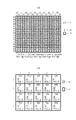
図17を用いて本実施例を説明する。図17(a)は、J行かつK列の行列状に配された複数の画素回路10の配置を示している。本実施例の画素回路10は、上述した実施例の有効画素11、OB画素15、リファレンス画素17のいずれかとすることができる。実用的には、J≧100、K≧100であり、より好ましくは、J≧1000、K≧1000である。画素回路10のJ行は、第a1〜a4行、第b1〜b4行、第c1〜c4行、第d1〜d4行をこの順で含む。第a1〜a4行は、第a1行、第a2行、第a3行、第a4行をこの順で含み、これらを第a行と総称する。第b1〜b4行を第b行と総称し、第c1〜c4行を第c行と総称し、第d1〜d4行を第d行と総称する。a、b、c、dは正の整数であり、a<b<c<dである。a1、a2、a3、a4は正の整数であり、a1<a2<a3<a4である。例えば、図17(a)に示した複数の画素回路10が全ての画素回路10であるとすれば、a1=1、a2=2、a3=3、a4=4、b1=5、b4=8、c1=9、c4=12、d1=13、d4J=16である。説明の上では、第a1〜d4行のそれぞれの行は隣接しているものとして説明する。行が隣接している場合、a2=1+a1、a3=1+a2、a4=1+a3であり、b1=1+a4、c1=1+b4、d1=1+c4である。しかし、2つの行の間に図示しない行があることを否定するものではない。
(Example 5)
This embodiment will be described with reference to FIG. FIG. 17A shows the arrangement of a plurality of
画素回路10のK列は、第e1列、第f1列、第g1列、第h1列、第e2列、第f2列、第g2列、第h2列をこの順で含む。すなわち、e1、f1、g1、h1、e2、f2、g2、h2は正の整数であり、e1<f1<g1<h1<e2<f2<g2<h2である。同様に、h2<e3<f3<g3<h3<e4<f4<g4<h4である。ある。例えば、図17に示した複数の画素回路10が全ての画素回路10であるとすれば、e1=1、f1=2、g1=3、h1=4、e2=5、f2=6、g2=7、h2=8、h5=K=20である。説明の上では、第e1〜h5行のそれぞれの行は隣接しているものとして説明する。列が隣接している場合、f1=1+e1、g1=1+f1、h1=1+g1であり、e2=1+h4、e3=1+h2、e4=1+h3、e5=1+h4である。しかし、2つの列の間に図示しない列があることを否定するものではない。
The K column of the
以降の説明では、第α行かつ第β行の画素回路10を画素回路10(α、β)と表現する。
In the following description, the
同一列の画素回路10の2つ以上の画素回路10が信号線14へ共通に接続されている。この信号線14は、上述した実施例の信号線201を適用することができる。信号線14は、同一列の画素回路10が並ぶ方向に沿って延びている。例えば、第e1列の画素回路10(a1、e1)、10(b1、e1)、10(c1、e1)、10(d1、e1)は、共通の信号線14に接続されている。同一列の画素回路10の全ての画素回路10が1本の信号線14に共通に接続されてもよいが、同一列の画素回路10の2つ以上の画素回路10が共通に接続される信号線14は複数本あってもよい。例えば、第e1列の画素回路10(a2、e1)、10(b2、e1)、10(c2、e1)、10(d2、e1)は、画素回路10(a1、e1)が接続された信号線14とは別の信号線14に共通に接続されてもよい。複数の信号線14に接続された複数の画素回路10は、信号線14に読み出すべき画素回路10から順番に選択されて、それぞれ読み出される。同一列の画素回路10からの信号を、複数の信号線14で並行して読み出すことで、信号の読出しを高速化できる。
Two or
また、図17(b)は、T行かつU列の行列状に配された複数の周辺回路20の配置を示している。周辺回路20は、上述した実施例の信号処理回路21を適用することができる。ここで、T<Jであり、U<Kである。実用的には、T≧10、U≧10であり、より好ましくは、T≦1000、U≦1000である。周辺回路20のT行は、第q行、第q行、第r行、第s行をこの順で含む。すなわち、p、q、r、sは正の整数でありp<q<r<sである。例えば、図17(b)に示した複数の周辺回路20が全ての周辺回路20であるとすれば、p=1、q=2、r=3、s=T=4である。説明の上では、第p〜s行のそれぞれの行は隣接しているものとして説明する。行が隣接している場合、q=1+p、r=1+q、s=1+rである。しかし、2つの行の間に図示しない行があることを否定するものではない。
Further, FIG. 17B shows the arrangement of a plurality of
周辺回路20のU列は、第v列、第w列、第x列、第y列、第z列をこの順で含む。すなわち、v、w、x、y、zは正の整数でありv<w<x<y<zである。例えば、図17に示した複数の周辺回路20が全ての周辺回路20であるとすれば、v=1、w=2、x=3、y=4、z=U=5である。説明の上では、第v〜z行のそれぞれの列は隣接しているものとして説明する。列が隣接している場合、w=1+v、x=1+w、y=1+x、z=1+yである。しかし、2つの列の間に図示しない列があることを否定するものではない。
The U column of the
以降の説明では、第γ行かつ第δ行の周辺回路20を周辺回路20(γ、δ)と表現する。
In the following description, the
第v列の周辺回路20は、第p行の周辺回路20(p、v)、第q行の周辺回路20(q、v)、第r行の周辺回路20(r、v)、第s行の周辺回路20(s、v)を含む。第w列の周辺回路20は、第p行の周辺回路20(p、w)、第q行の周辺回路20(q、w)、第r行の周辺回路20(r、w)、第s行の周辺回路20(s、v)を含む。
The
同一の周辺回路20に接続される画素回路10の集合を画素グループ15と称する。本例では、画素グループ15は、J個の画素回路10からなる。1つの画素グループ15には、当該1つの画素グループ15に所属する全ての画素回路10が同一の周辺回路20に接続される。そして、当該同一の周辺回路20には、当該画素グループ15以外の画素グループ15に含まれる画素回路10は接続されない。本実施例では、同一列の画素回路10の複数の画素回路10が画素グループ15を構成する。本例では、1つの画素グループ15には同一列の全ての画素回路10が属する。例えば、第e1列の全ての画素回路10は画素グループ15e1に属する。図17(a)には、第α列の画素回路10で構成される画素グループ15を画素グループ15αと表現している(αはe1、f1、e2などである)。
A set of
図17(b)には、周辺回路20の各々が、複数の画素ブロック15のうちのどの画素ブロック15に接続されるかを示している。例えば、周辺回路20(p、v)は画素ブロック15e1に接続されており、周辺回路20(q、v)は画素ブロック15f1に接続されている。周辺回路20(r、v)は画素ブロック15f1に接続されており、周辺回路20(s、v)は画素ブロック15g1に接続されている。例えば、周辺回路20(p、w)は画素ブロック15e2に接続されており、周辺回路20(q、w)は画素ブロック15f2に接続されている。周辺回路20(r、w)は画素ブロック15g2に接続されており、周辺回路20(s、w)は画素ブロック15h2に接続されている。例えば、周辺回路20(p、x)は画素ブロック15e3に接続されており、周辺回路20(q、x)は画素ブロック15f3に接続されている。周辺回路20(r、x)は画素ブロック15g3に接続されており、周辺回路20(s、x)は画素ブロック15h3に接続されている。
FIG. 17B shows which of the plurality of pixel blocks 15 each of the
図17に示す例では、同一列の画素回路10の全ての画素回路10が同一の画素グループ15に属する。そのため、第e1列の全ての画素回路10は周辺回路20(p、v)に接続され、第f1列の全ての画素回路10は周辺回路20(q、v)に接続されている。第g1列の全ての画素回路10は周辺回路20(r、v)に接続され、第h1列の全ての画素回路10は周辺回路20(s、v)に接続されている。第e2列の全ての画素回路10は周辺回路20(p、w)に接続され、第f2列の全ての画素回路10は周辺回路20(q、w)に接続されている。第g2列の全ての画素回路10は周辺回路20(r、w)に接続され、第h2列の全ての画素回路10は周辺回路20(s、w)に接続されている。第e3列の全ての画素回路10は周辺回路20(p、x)に接続され、第f3列の全ての画素回路10は周辺回路20(q、x)に接続されている。第g3列の全ての画素回路10は周辺回路20(r、x)に接続され、第h3列の全ての画素回路10は周辺回路20(s、x)に接続されている。
In the example shown in FIG. 17, all the
ここで、同一行(例えば第a行)の3列分(例えば第e1〜g1列、)の画素回路10と、3列分の画素回路10に接続された同一列(例えばv列)の3行分(例えば第p〜r行)の周辺回路20に注目する。3列分の画素回路10のうちの中間の列(第f1列)の画素回路10は、3行分の周辺回路20のうちの中間の列(第q行)の周辺回路20に接続されている。このようにすることで、3列分の画素回路10の並び順と、この3列分の画素回路10のそれぞれが接続された3行分の周辺回路20の並び順が一致する。このようにすることで、周辺回路20による信号処理の特性の違いの影響を小さくできる。3行分の周辺回路20に関して、中間の行の周辺回路20と一端の行の周辺回路20との特性差、および、中間の行の周辺回路20と他端の行の周辺回路20との特性差を、第1の特性差と称する。一端の行の周辺回路20と他端の行の周辺回路20の特性差を第2の特性差と称する。2つの周辺回路20の特性差はその距離に比例するため、第1の特性差は第2の特性差よりも小さくなる傾向にある。3列分の画素回路10に関して、中間の列の画素回路10と一端の列の画素回路10の出力差、および、中間の列の画素回路10との他端の列の画素回路10の出力差は、第1の特性差に対応することになる。そのため、2つの画素回路10に対応した信号の出力差を小さくする上では、2つの画素回路10の間の距離が小さいほど、対応する2つの周辺回路20の間の距離を小さくすることが好ましいのである。
Here, 3 of the
このことは、f1がe1とg1の間の整数であり、qがpとrの間の整数であることに対応する。また、f1がe1とh1の間の整数であり、qがpとsの間の整数であることに対応する。また、g1がe1とh1の間の整数であり、rがqとsの間の整数であることに対応する。また、g1がf1とh1の間の整数であり、rがqとsの間の整数であることに対応する。ここでは、第a行、第v列を例示したが、第b行、第c行、第d行でも同様であり、第w列、第x列、第y列、第z列でも同様である。 This corresponds to f1 being an integer between e1 and g1 and q being an integer between p and r. It also corresponds to f1 being an integer between e1 and h1 and q being an integer between p and s. It also corresponds to g1 being an integer between e1 and h1 and r being an integer between q and s. It also corresponds to g1 being an integer between f1 and h1 and r being an integer between q and s. Here, the ath row and the vth column are illustrated, but the same applies to the bth row, the cth row, and the dth row, and the same applies to the wth column, the xth column, the yth column, and the zth column. ..
本実施例では、e1<f1<g1<h1、p<q<r<sであることから、周辺回路20の列番が同じ場合には、画素回路10の列番が大きくなるほど、接続される周辺回路20の行番が大きくなる。
In this embodiment, since e1 <f1 <g1 <h1 and p <q <r <s, when the column numbers of the
複数の画素回路10と複数の周辺回路20との接続関係を説明する。
The connection relationship between the plurality of
図17に示す例では、第a列の全ての画素回路10は周辺回路20(i、j)に接続され、第b列の全ての画素回路10は周辺回路20(k、j)に接続され、第c列の全ての画素回路10は周辺回路20(s、j)に接続されている。第d列の全ての画素回路10は周辺回路20(i、r)に接続され、第e列の全ての画素回路10は周辺回路20(k、r)に接続され、第f列の全ての画素回路10は周辺回路20(s、r)に接続されている。第g列の全ての画素回路10は周辺回路20(i、t)に接続され、第h列の全ての画素回路10は周辺回路20(k、t)に接続され、第q列の全ての画素回路10は周辺回路20(s、t)に接続されている。
In the example shown in FIG. 17, all the
本実施例では、e1<f1<g1<h1であることから、周辺回路20の列番が同じ場合には、画素回路10の列番が大きくなるほど、接続される周辺回路20の行番が大きくなることになる。
In this embodiment, since e1 <f1 <g1 <h1, when the column numbers of the
h1<e2であることから、画素回路10の列番が大きくなる(第h1列から第e2列になる)と、接続される周辺回路20の列番が変わる(第v列から第w列になる)。同一列の周辺回路20に割り当てられる画素回路10の列数はe2−h1+1であり、これが同一列に含まれる周辺回路20の行数Tに等しくなる(T=e2−h1+1)。換言すれば、Tに等しい画素回路10の列数毎に、接続される周辺回路20の列が変わるのである。
Since h1 <e2, when the column number of the
本実施例では、同一行(例えば第p行)かつ近接列(例えば第v行と第w行)の周辺回路20がそれぞれ接続された2つの画素回路10(例えば第e1列と第e2列)の間にはT−1列分の画素回路10が存在する。
In this embodiment, two pixel circuits 10 (for example, columns e1 and e2) to which
また、K列の画素回路10が列毎にいずれかの周辺回路20に割り当てられる。そのため、T×U=Kとなりうる。信号処理の並列度を高めるためには、J≦Kとすることが好ましいため、J≦T×Uとなる。また、T<J、U<Kであるから、T×U<J×Kである。よって、T×U−K<J×K−T×Uを満たす。これを変形すると、T×U<(J+1)×K/2となり、J+1≒Jであるから、T×U<J×K/2となる。よって、本実施例の接続方法を採用する場合には、J≦T×U<J×K/2を満足することが好ましい。
Further, the
図18には、画素回路10と周辺回路20の平面的な位置関係を示している。図18では、複数の画素回路10を構成する複数の半導体素子100と、複数の周辺回路20を構成する複数の半導体素子200と、を示している。なお、半導体素子100のうちの特定の半導体素子を半導体素子101〜106で示し、半導体素子200のうちの特定の半導体素子を半導体素子201〜206で示している。複数の半導体素子100の何れかは、接続部300を介して、複数の半導体素子200の何れかに電気的に接続されている。半導体素子101〜106と半導体素子201〜206とを接続する特定の接続部を接続部301〜306で指名している。
FIG. 18 shows the planar positional relationship between the
図17の太線は、半導体素子100と半導体素子200との間の配線経路を示している。半導体素子100と半導体素子200とを接続する配線経路は、半導体素子100と接続部300とを接続する配線経路と、接続部300と半導体素子200とを接続する配線経路とに区別することができる。
The thick line in FIG. 17 shows the wiring path between the
図17に示した、半導体素子100と半導体素子200の間の接続部300を介した配線経路は、実際の配線経路の長さの大小関係を模式的に示している。v列目の周辺回路20(p、v)、20(r、v)、20(s、v)と、このv列目の周辺回路20(p、v)、20(r、v)、20(s、v)に接続された画素回路10との間の配線経路に注目する。1つの半導体素子100と1つの半導体素子200との間の最短の配線経路の長さは、画素回路10毎および/または周辺回路20毎に互いに異なっている。図17には、画素回路10(a1、e1)の半導体素子101と周辺回路20(p、v)の半導体素子201との間の最短の配線経路の長さL1を示している。
The wiring path via the
なお、半導体素子201には、信号線14aを介して、画素回路10(c1、e1)の半導体素子100も接続されている。しかし、画素回路10(a1、e1)の半導体素子100と半導体素子201との間の配線経路は、画素回路10(a1、e1)の半導体素子101と周辺回路(p、v)の半導体素子201との間の配線経路よりも長い。そのため、画素回路10(c1、e1)の半導体素子10と半導体素子201との間の配線経路は、画素回路10の半導体素子100と半導体素子201との間の最短の配線経路ではない。以降の説明では、他の配線経路についても、同様にして最短の配線経路を特定する。
The
図17には、画素回路10(a4、e1)の半導体素子102と周辺回路20(p、v)の半導体素子202との間の最短の配線経路の長さL2を示している。画素回路10(d1、h1)の半導体素子103と周辺回路20(s、v)の半導体素子203との間の最短の配線経路の長さL3を示している。画素回路10(d1、h1)の半導体素子104と周辺回路20(s、v)の半導体素子204との間の最短の配線経路の長さL4を示している。
FIG. 17 shows the length L2 of the shortest wiring path between the
長さL3および長さL4は、長さL1および長さL2よりも大きい(L1、L2<L3、L4)。このように、画素回路10と周辺回路20との間の配線経路の長さを周辺回路20毎に異ならせることで、画素回路10のレイアウトと周辺回路20のレイアウトの自由度を高めている。特に、より長い配線経路を採用することで、画素回路10の半導体素子100から離れた位置に、周辺回路20の半導体素子200を配置できる。そのため、より長い配線経路は画素回路10のレイアウトと周辺回路20のレイアウトの自由度を高めることに大いに貢献している。
The length L3 and the length L4 are larger than the length L1 and the length L2 (L1, L2 <L3, L4). In this way, by making the length of the wiring path between the
長さL2は長さL1よりも小さい(L2<L1)。また、長さL4は長さL3よりも大きい(L3<L4)。このように、画素回路10と周辺回路20との間の配線経路の長さを画素回路10毎に異ならせることで、画素回路10のレイアウトと周辺回路20のレイアウトの自由度を高めている。特に、より長い配線経路を採用することで、画素回路10の半導体素子100から離れた位置に、周辺回路20の半導体素子200を配置できる。そのため、より長い配線経路は画素回路10のレイアウトと周辺回路20のレイアウトの自由度を高めることに大いに貢献している。
The length L2 is smaller than the length L1 (L2 <L1). Further, the length L4 is larger than the length L3 (L3 <L4). In this way, by making the length of the wiring path between the
図17には、画素回路10(c1、g1)の半導体素子105と周辺回路20(r、v)の半導体素子205との間の最短の配線経路の長さL5を示している。また、画素回路10(c1、g1)の半導体素子106と周辺回路20(r、v)の半導体素子206との間の最短の配線経路の長さL6を示している。長さL5、L6は、長さL1、L2と長さL3、L4との間の長さである(L1、L2<L5、L6<L3、L4)。このように、配線経路の長さを3種類以上にすることで、隣接する周辺回路20同士での、配線経路の長さの違いに起因する電気特性の違いを低減することができる。また、周辺回路20の電気特性の違いを信号処理により補正する場合に、行が進むにつれて配線経路が長くなるようにしておけば、補正のアルゴリズムを簡略化することができる。
FIG. 17 shows the length L5 of the shortest wiring path between the
ここまで、第v列の周辺回路20に関して説明したが、図17から理解できるように、第w列、第x列の周辺回路20の配線経路についても同様である。
Up to this point, the
ここで、配線経路について、より詳細に説明する。図18は、半導体装置APRの断面図である。配線構造12は5層(M層)の配線層を含む。5層(M層)の配線層は、半導体層11から、1番目の配線層121、2番目(m番目)の配線層122、3番目(m”番目;m<m”<m’)の配線層123、4番目(m’番目;m’>m)の配線層124、5番目(M番目)の配線層125である。配線構造22は5層(M層)の配線層を含む。
Here, the wiring path will be described in more detail. FIG. 18 is a cross-sectional view of the semiconductor device APR. The
配線構造22は6層(N層)の配線層を含む。6層(N層)の配線層は、半導体層21から、1番目の配線層221、2番目の配線層222、3番目(n番目)の配線層223、4番目(N−2番目)の配線層224、5番目(N−1番目)の配線層225、6番目(N番目)の配線層225を含む。
The
導電部131、133は、配線構造12の半導体層11からM番目の配線層125に含まれ、配線構造12によって複数の画素回路10のうちの任意の画素回路(α、β)に接続されている。導電部231、233は、配線構造22の半導体層21からN番目の配線層226に含まれ、配線構造22によって複数の周辺回路20のうちの任意の周辺回路(γ、δ)に接続されている。導電部131と導電部231とが電気的に接続されており、導電部133と導電部233とが電気的に接続されている。導電部131と導電部231とを合わせたものが接続部301であり、導電部133と導電部233とを合わせたものが接続部303である。他の接続部300も同様に、配線構造12の導電部と、配線構造22の導電部とが電気的に接続されたものである。具体的には、導電部131、133と導電部231、233はそれぞれ銅を主成分としており、導電部131の銅と導電部231の銅とが接合しており、導電部133の銅と導電部233の銅とが接合している。この他の形態としては、導電部131と導電部231との間と、導電部133と導電部233との間と、にそれぞれ配置したバンプを介して導電部131と導電部231、233とを電気的に接続することができる。また、別の形態としては、半導体層21を貫通する貫通電極を用いて導電部131、133と導電部231、233とを接続することができる。いずれの接続形態においても、導電部131および導電部231は、半導体層11と周辺回路20(p、v)との間に位置している。また、導電部133および導電部233は、半導体層11と周辺回路20(s、v)との間に位置している。
The
なお、M層目の配線層125とN層目の配線層226とが接しない場合、M層目の配線層125とN層目の配線層226との間に、画素回路10と周辺回路20のどちらも構成しない配線層を配置することもできる。
When the
半導体素子100、200は、例えばソース/ドレインとゲートを有するトランジスタであるが、ダイオードでもよい。半導体素子100、200の導電部131、133が接続する部分は、半導体素子100、200のソース/ドレインでもよいし、ゲートであってもよい。また、半導体素子100、200はMIS型の容量素子や、多結晶シリコンや単結晶シリコンからなる抵抗素子であってもよい。
The
図18に示すように、半導体層11の上であって、半導体層11に対して配線構造12側とは反対側には、カラーフィルタアレイ17および/またはマイクロレンズアレイ18を含む光学構造19が設けられている。
As shown in FIG. 18, an
導電部231から複数の画素回路10を構成する複数の半導体素子100までの最短の配線経路の長さが長さL11である。ここでは、最短の配線経路の長さとなるのは、導電部231から半導体素子101までの配線経路である。導電部131から複数の周辺回路20を構成する複数の半導体素子200までの最短の配線経路の長さが長さL12である。ここでは、最短の配線経路の長さとなるのは、導電部231から半導体素子201までの配線経路である。上述した長さL1はL11とL12との和(L1=L11+L12)におおむね相当する。導電部233から複数の画素回路10を構成する複数の半導体素子100までの最短の配線経路の長さが長さL31である。ここでは、最短の配線経路の長さとなるのは、導電部231から半導体素子103までの配線経路である。導電部133から複数の周辺回路20を構成する複数の半導体素子200までの最短の配線経路の長さが長さL32である。ここでは、最短の配線経路の長さとなるのは、導電部231から半導体素子203までの配線経路である。上述した長さL3はL31とL32との和(L3=L31+L32)におおむね相当する。
The length of the shortest wiring path from the
なお、長さL11の算定の始点を導電部231とし、長さL12の算定の始点を導電部131とすることで、配線経路の長さには、導電部131と導電部133との間の接続距離が2倍されて含まれ得る。しかし、配線経路の長さの比較においては、導電部131と導電部133との間の接続距離を相殺することができる。
By setting the starting point of the calculation of the length L11 as the
互いに接続された導電部131と導電部231に関し、導電部231から半導体素子100までの配線経路の長さL11は、導電部131から半導体素子200までの配線経路の長さL12よりも大きい(L11>L12)。同様に、互いに接続された導電部133と導電部233に関し、導電部233から半導体素子100までの配線経路の長さL31は、導電部133から半導体素子200までの配線経路の長さL32よりも大きい(L31>L32)。なお、長さL2については、接続部302から半導体素子102までの配線経路の長さが接続部302から半導体素子202までの配線経路の長さ以下である。さらに、本例では、長さL31が長さL12よりも大きい(L12<L31)。長さL11が長さL32よりも大きい(L32<L11)。
Regarding the conductive portion 131 and the
このように、接続部300からの配線経路の長さを、接続部300に対して配線構造22側よりも、配線構造12側で大きくすることが好ましい。具体的には、配線経路を延長するための配線を配線構造12に設ければよい。配線経路を延長することで、配線に混入するノイズが増大しうる。しかし、配線経路を延長するための配線を配線構造12に設け、配線経路を配線構造22側で長くすることで、ノイズ源となる周辺回路20から離すことができる。これにより、半導体素子100と半導体素子200との間の配線経路に生じるノイズを抑制できる。
As described above, it is preferable that the length of the wiring path from the
また、周辺回路20毎の特性のばらつきを低減するためには、周辺回路20毎の半導体素子200の位置関係のばらつきを小さくすることが好ましい。周辺回路20毎の半導体素子200の位置関係のばらつきが大きくなれば、その分、周辺回路20内のレイアウトが異なり、レイアウトの違いによる特性のばらつきが大きくなるからである。本例では、周辺回路20における半導体素子200の位置関係は、周辺回路20毎に同じである。そして、接続部300から半導体素子200までの配線経路はできるだけ短くなっている。本例では、長さL31が長さL12よりも大きい(L12<L31)。長さL11が長さL32よりも大きい(L32<L11)。さらに、長さL12と長さL32は等しい(L12=L32)。このようにすれば、接続部300から半導体素子200までの配線経路の長さによる、周辺回路20の特性ばらつきを低減できるため、好ましい。
Further, in order to reduce the variation in the characteristics of each
配線経路を延長するための配線は、配線構造12と配線構造22のうち、配線層数が小さい方の配線構造に含まれることが好ましい。配線経路を延長するための配線層を設けた結果、配線構造12と配線構造22の配線層数が同じとなってもよい。配線経路を延長するための配線層が、配線構造12と配線構造22のうち、配線層数が大きい方の配線構造に含まれると、歩留まりが低下したりコストが増大したりする可能性が高くなるためである。配線構造12と配線構造22のうち、配線層数が少ない方の配線構造であれば、配線経路を延長するための配線を配置しても、歩留まりの低下やコストの増大を抑制できる。
The wiring for extending the wiring path is preferably included in the wiring structure having the smaller number of wiring layers among the
これらの点を総合すると、L12<L11とし、L32<L31とする場合には、配線構造12の配線層数(M)は、配線構造22の配線層数(N)以下であること(M≦N)が好ましい。配線構造12の配線層数(M)は、配線構造22の配線層数(N)よりも小さいこと(M<N)が好ましい。
When these points are put together, when L12 <L11 and L32 <L31, the number of wiring layers (M) of the
図18に示す形態では、複数の画素回路のうちの2つ以上の画素回路が共通に接続された共通線421、422、423、424は、2番目(m番目)の配線層122に含まれている。図18には、共通線421、423と導電部131、133とを接続する延長線441、442を示している。延長線441、443は、共通線421、423と導電部131、133との間の配線経路を延長するために設けられた配線である。延長線441、443の配線長が、長さL11、L13の大半、さらには、長さL1、L3の大半を担いうる。図18に示す形態では、延長線441、443は、4番目(m’番目;m’>m)の配線層124に含まれている。配線経路を延長するための延長線441、442は低抵抗であることが好ましいため、配線の幅を太くしやすい、より上層の配線層に設けることが好ましい。
In the embodiment shown in FIG. 18, the common lines 421, 422, 423, and 424 in which two or more pixel circuits among the plurality of pixel circuits are commonly connected are included in the second (mth)
延長線441、443と共通線422、424との間には、シールド線431、432、433が配されている。シールド線431、432、433は、接地電位や電源電位などの固定電位が供給された配線である。シールド線431、432、433は、延長線441、443を含む4番目(m’番目;m’>m)の配線層124と、共通線422、424を含む2番目(m番目)の配線層122との間に位置する。シールド線431、432、433は、3番目(m”番目;m<m”<m’)の配線層123に含まれる。共通線421と共通線422は別々の信号を伝送する。そのため、共通線421に接続された延長線441が共通線422に近接(例えば交差)すると、共通線421の信号と共通線422の信号との間でクロストークが生じ得る。そこで、延長線441と共通線422との間に、固定電位が供給されたシールド線431を配置することで、クロストークを抑制できる。同様に、シールド線433は、共通線423に接続された延長線443と共通線424との間に配され、共通線423の信号と共通線424の信号とのクロストークを抑制できる。
Shielded
(実施例6)
図19を用いて本実施例を説明するが、実施例5と同じである点については省略する。例えば、接続部303を介した半導体素子103と半導体素子203との間の配線経路の長さL3は、接続部301を介した半導体素子101と半導体素子201との間の配線経路の長さL1よりも大きい点で同じである。
(Example 6)
This embodiment will be described with reference to FIG. 19, but the same points as in the fifth embodiment will be omitted. For example, the length L3 of the wiring path between the
実施例5では、接続部300から半導体素子200までの配線経路の長さ(例えば長さL12、L32)を周辺回路20毎に同じにした(L12=L32)。これに対し、本実施例では、長さL12、L32を周辺回路20毎に異ならせている。例えば、長さL32は長さL12より大きい(L12<L32)。このようにすることで、接続部300を、半導体素子200の位置に制限されずに、適切な位置に配置することが可能となる。その結果、周辺回路20の特性のばらつきを低減できる。また、接続部300の位置を最適化することで、接続部300における接合ムラを低減できるため、接続部300の接続の信頼性を向上できる。
In the fifth embodiment, the length of the wiring path from the
本実施例では、実施例5と同様に、接続部301を介した半導体素子101と半導体素子201との間の配線経路については長さL11が長さL12よりも大きい(L12<L11)。そのため、延長線441を配線構造12に配置すればよい。一方、実施例5とは異なり、接続部303を介した半導体素子103と半導体素子203との間の配線経路については、長さL32が長さL31よりも大きい(L31<L32)。そのため、延長線443だけではなく、配線構造22にも延長線が追加される。
In this embodiment, as in the fifth embodiment, the length L11 is larger than the length L12 for the wiring path between the
(実施例7)
図20は、本実施例による撮像システム500の構成を示すブロック図である。本実施例の撮像システム500は、上述の各実施例で述べた撮像装置のいずれかの構成を適用した撮像装置200を含む。撮像システム500の具体例としては、デジタルスチルカメラ、デジタルカムコーダー、監視カメラ等が挙げられる。図20に、上述の各実施例のいずれかの撮像装置を撮像装置200として適用したデジタルスチルカメラの構成例を示す。
(Example 7)
FIG. 20 is a block diagram showing the configuration of the
図20に例示した撮像システム500は、撮像装置200、被写体の光学像を撮像装置200に結像させるレンズ5020、レンズ5020を通過する光量を可変にするための絞り504、レンズ5020の保護のためのバリア506を有する。レンズ5020及び絞り504は、撮像装置200に光を集光する光学系である。
The
撮像システム500は、また、撮像装置200から出力される出力信号の処理を行う信号処理部5080を有する。信号処理部5080は、必要に応じて入力信号に対して各種の補正、圧縮を行って出力する信号処理の動作を行う。信号処理部5080は、撮像装置200より出力される出力信号に対してAD変換処理を実施する機能を備えていてもよい。この場合、撮像装置200の内部には、必ずしもAD変換回路を有する必要はない。
The
撮像システム500は、更に、画像データを一時的に記憶するためのバッファメモリ部510、外部コンピュータ等と通信するための外部インターフェース部(外部I/F部)512を有する。更に撮像システム500は、撮像データの記録又は読み出しを行うための半導体メモリ等の記録媒体514、記録媒体514に記録又は読み出しを行うための記録媒体制御インターフェース部(記録媒体制御I/F部)516を有する。なお、記録媒体514は、撮像システム500に内蔵されていてもよく、着脱可能であってもよい。
The
更に撮像システム500は、各種演算を行うとともにデジタルスチルカメラ全体を制御する全体制御・演算部518、撮像装置200と信号処理部5080に各種タイミング信号を出力するタイミング発生部520を有する。ここで、タイミング信号などは外部から入力されてもよく、撮像システム500は、少なくとも撮像装置200と、撮像装置200から出力された出力信号を処理する信号処理部5080とを有すればよい。全体制御・演算部518及びタイミング発生部520は、撮像装置200の制御機能の一部又は全部を実施するように構成してもよい。
Further, the
撮像装置200は、画像用信号を信号処理部5080に出力する。信号処理部5080は、撮像装置200から出力される画像用信号に対して所定の信号処理を実施し、画像データを出力する。また、信号処理部5080は、画像用信号を用いて、画像を生成する。
The
上述した各実施例の撮像装置による撮像装置を用いて撮像システムを構成することにより、より良質の画像が取得可能な撮像システムを実現することができる。 By configuring the image pickup system by using the image pickup device by the image pickup device of each of the above-described embodiments, it is possible to realize an image pickup system capable of acquiring a higher quality image.
(実施例8)
本実施例の撮像システム及び移動体について、図21及び図22を用いて説明する。
(Example 8)
The image pickup system and the moving body of this embodiment will be described with reference to FIGS. 21 and 22.
図21は、本実施例による撮像システム及び移動体の構成例を示す概略図である。図22は、本実施例による撮像システムの動作を示すフロー図である。 FIG. 21 is a schematic view showing a configuration example of an imaging system and a moving body according to the present embodiment. FIG. 22 is a flow chart showing the operation of the imaging system according to the present embodiment.
本実施例では、車載カメラに関する撮像システムの一例を示す。図21は、車両システムとこれに搭載される撮像システムの一例を示したものである。撮像システム701は、撮像装置702、画像前処理部715、集積回路703、光学系714を含む。光学系714は、撮像装置702に被写体の光学像を結像する。撮像装置702は、光学系714により結像された被写体の光学像を電気信号に変換する。撮像装置702は、上述の各実施例のいずれかの撮像装置である。画像前処理部715は、撮像装置702から出力された信号に対して所定の信号処理を行う。画像前処理部715の機能は、撮像装置702内に組み込まれていてもよい。撮像システム701には、光学系714、撮像装置702及び画像前処理部715が、少なくとも2組設けられており、各組の画像前処理部715からの出力が集積回路703に入力されるようになっている。
In this embodiment, an example of an imaging system related to an in-vehicle camera is shown. FIG. 21 shows an example of a vehicle system and an imaging system mounted on the vehicle system. The
集積回路703は、撮像システム用途向けの集積回路であり、メモリ705を含む画像処理部704、光学測距部706、視差演算部707、物体認知部708、異常検出部709を含む。画像処理部704は、画像前処理部715の出力信号に対して、現像処理や欠陥補正等の画像処理を行う。メモリ705は、撮像画像の一次記憶、撮像画素の欠陥位置を格納する。光学測距部706は、被写体の合焦や、測距を行う。視差演算部707は、複数の撮像装置702により取得された複数の画像データから視差(視差画像の位相差)の算出を行う。物体認知部708は、車、道、標識、人等の被写体の認知を行う。異常検出部709は、撮像装置702の異常を検出すると、主制御部713に異常を発報する。
The
集積回路703は、専用に設計されたハードウェアによって実現されてもよいし、ソフトウェアモジュールによって実現されてもよいし、これらの組合せによって実現されてもよい。また、FPGA(Field Programmable Gate Array)やASIC(Application Specific Integrated Circuit)等によって実現されてもよいし、これらの組合せによって実現されてもよい。
The
主制御部713は、撮像システム701、車両センサ710、制御ユニット720等の動作を統括・制御する。なお、主制御部713を持たず、撮像システム701、車両センサ710、制御ユニット720が個別に通信インターフェースを有して、それぞれが通信ネットワークを介して制御信号の送受を行う(例えばCAN規格)方法も取りうる。
The
集積回路703は、主制御部713からの制御信号を受け或いは自身の制御部によって、撮像装置702へ制御信号や設定値を送信する機能を有する。例えば、集積回路703は、撮像装置702内の電圧スイッチ13をパルス駆動させるための設定や、フレーム毎に電圧スイッチ13を切り替える設定等を送信する。
The
撮像システム701は、車両センサ710に接続されており、車速、ヨーレート、舵角などの自車両走行状態及び自車外環境や他車・障害物の状態を検出することができる。車両センサ710は、視差画像から対象物までの距離情報を取得する距離情報取得手段でもある。また、撮像システム701は、自動操舵、自動巡行、衝突防止機能等の種々の運転支援を行う運転支援制御部711に接続されている。特に、衝突判定機能に関しては、撮像システム701や車両センサ710の検出結果を基に他車・障害物との衝突推定・衝突有無を判定する。これにより、衝突が推定される場合の回避制御、衝突時の安全装置起動を行う。
The
また、撮像システム701は、衝突判定部での判定結果に基づいて、ドライバーに警報を発する警報装置712にも接続されている。例えば、衝突判定部の判定結果として衝突可能性が高い場合、主制御部713は、ブレーキをかける、アクセルを戻す、エンジン出力を抑制するなどして、衝突を回避、被害を軽減する車両制御を行う。警報装置712は、音等の警報を鳴らす、カーナビゲーションシステムやメーターパネルなどの表示部画面に警報情報を表示する、シートベルトやステアリングに振動を与えるなどしてユーザに警告を行う。
The
本実施例では、車両の周囲、例えば前方又は後方を撮像システム701で撮影する。図21(b)に、車両前方を撮像システム701で撮像する場合の撮像システム701の配置例を示す。
In this embodiment, the surroundings of the vehicle, for example, the front or the rear, are photographed by the
2つの撮像装置702は、車両700の前方に配置される。具体的には、車両700の進退方位又は外形(例えば車幅)に対する中心線を対称軸に見立て、その対称軸に対して2つの撮像装置702が線対称に配置されると、車両700と被写対象物との間の距離情報の取得や衝突可能性の判定を行う上で好ましい。また、撮像装置702は、運転者が運転席から車両700の外の状況を視認する際に運転者の視野を妨げない配置が好ましい。警報装置712は、運転者の視野に入りやすい配置が好ましい。
The two
次に、撮像システム701における撮像装置702の故障検出動作について、図22を用いて説明する。撮像装置702の故障検出動作は、図22に示すステップS810〜S880に従って実施される。
Next, the failure detection operation of the
ステップS810は、撮像装置702のスタートアップ時の設定を行うステップである。すなわち、撮像システム701の外部(例えば主制御部713)又は撮像システム701の内部から、撮像装置702の動作のための設定を送信し、撮像装置702の撮像動作及び故障検出動作を開始する。
Step S810 is a step for setting the start-up of the
次いで、ステップS820において、有効画素から画素信号を取得する。また、ステップS830において、故障検出用に設けた故障検出画素からの出力値を取得する。この故障検出画素は、有効画素と同じく光電変換部を備える。この光電変換部には、所定の電圧が書き込まれる。故障検出用画素は、この光電変換部に書き込まれた電圧に対応する信号を出力する。なお、ステップS820とステップS830とは逆でもよい。 Next, in step S820, a pixel signal is acquired from the effective pixel. Further, in step S830, the output value from the failure detection pixel provided for failure detection is acquired. The failure detection pixel includes a photoelectric conversion unit like the effective pixel. A predetermined voltage is written in this photoelectric conversion unit. The failure detection pixel outputs a signal corresponding to the voltage written in the photoelectric conversion unit. The steps S820 and S830 may be reversed.
次いで、ステップS840において、故障検出画素の出力期待値と、実際の故障検出画素からの出力値との該非判定を行う。 Next, in step S840, the non-determination of the expected output value of the failure detection pixel and the output value from the actual failure detection pixel is performed.
ステップS840における該非判定の結果、出力期待値と実際の出力値とが一致している場合は、ステップS850に移行し、撮像動作が正常に行われていると判定し、処理ステップがステップS860へと移行する。ステップS860では、走査行の画素信号をメモリ705に送信して一次保存する。そののち、ステップS820に戻り、故障検出動作を継続する。 If the expected output value and the actual output value match as a result of the non-determination in step S840, the process proceeds to step S850, it is determined that the imaging operation is normally performed, and the processing step proceeds to step S860. And migrate. In step S860, the pixel signal of the scanning line is transmitted to the memory 705 and primarily stored. After that, the process returns to step S820 and the failure detection operation is continued.
一方、ステップS840における該非判定の結果、出力期待値と実際の出力値とが一致していない場合は、処理ステップはステップS870に移行する。ステップS870において、撮像動作に異常があると判定し、主制御部713、又は警報装置712に警報を発報する。警報装置712は、表示部に異常が検出されたことを表示させる。その後、ステップS880において撮像装置702を停止し、撮像システム701の動作を終了する。
On the other hand, if the expected output value and the actual output value do not match as a result of the non-determination in step S840, the processing step proceeds to step S870. In step S870, it is determined that there is an abnormality in the imaging operation, and an alarm is issued to the
なお、本実施例では、1行毎にフローチャートをループさせる例を例示したが、複数行毎にフローチャートをループさせてもよいし、1フレーム毎に故障検出動作を行ってもよい。 In this embodiment, an example in which the flowchart is looped for each line is illustrated, but the flowchart may be looped for each of a plurality of lines, or the failure detection operation may be performed for each frame.
なお、ステップS870の警報の発報は、無線ネットワークを介して、車両の外部に通知するようにしてもよい。 The alarm in step S870 may be notified to the outside of the vehicle via the wireless network.
また、本実施例では、他の車両と衝突しない制御を説明したが、他の車両に追従して自動運転する制御や、車線からはみ出さないように自動運転する制御などにも適用可能である。さらに、撮像システム701は、自車両等の車両に限らず、例えば、船舶、航空機或いは産業用ロボットなどの移動体(移動装置)に適用することができる。加えて、移動体に限らず、高度道路交通システム(ITS)等、広く物体認識を利用する機器に適用することができる。
Further, in this embodiment, the control that does not collide with other vehicles has been described, but it can also be applied to the control that automatically drives following other vehicles and the control that automatically drives so as not to go out of the lane. .. Further, the
[変形実施例]
本発明は、上記実施例に限らず種々の変形が可能である。
[Modification Example]
The present invention is not limited to the above embodiment, and various modifications are possible.
例えば、いずれかの実施例の一部の構成を他の実施例に追加した例や、他の実施例の一部の構成と置換した例も、本発明の実施例である。 For example, an example in which a partial configuration of any of the examples is added to another embodiment or an example in which a partial configuration of another embodiment is replaced is also an example of the present invention.
また、上述の実施例は、いずれも本発明を実施するにあたっての具体化の例を示したものに過ぎず、これらの例示によって本発明の技術的範囲が限定的に解釈されてはならない。すなわち、本発明はその技術思想、又はその主要な特徴から逸脱することなく、様々な態様で実施することができる。 In addition, the above-mentioned examples are merely examples of embodiment in carrying out the present invention, and the technical scope of the present invention should not be construed in a limited manner by these examples. That is, the present invention can be carried out in various embodiments without departing from the technical idea or its main features.
1 第1チップ
5 第2チップ
11 画素
21 信号処理回路
830 有効画素領域
812A 水平OB画素領域
812B 垂直OB画素領域
835 リファレンス画素領域
1
Claims (22)
前記第1行に配された複数のオプティカルブラック画素が配された領域とを有する第1チップと、
前記複数のオプティカルブラック画素が出力する信号をAD変換する複数のAD変換部を有する第2チップとが積層された撮像装置であって、
前記AD変換部が、前記オプティカルブラック画素に対して、平面視において重なる部分を備え、
前記複数のAD変換部の、前記第1行の行に沿った方向における幅が、前記領域の、前記方向における幅よりも小さいことを特徴とする撮像装置。 In the first row, the effective pixels arranged over multiple columns,
A first chip having a region in which a plurality of optical black pixels arranged in the first row are arranged, and a first chip.
An image pickup apparatus in which a second chip having a plurality of AD conversion units for AD conversion of a signal output by the plurality of optical black pixels is laminated.
The AD conversion unit includes a portion that overlaps the optical black pixel in a plan view.
An image pickup apparatus characterized in that the width of the plurality of AD conversion units in a direction along the first row is smaller than the width of the region in the direction.
前記第1行に配された複数のオプティカルブラック画素が配された領域とを有する第1チップと、
前記複数のオプティカルブラック画素が出力する信号をAD変換する複数のAD変換部を有する第2チップとが積層された撮像装置であって、
前記AD変換部が、前記オプティカルブラック画素に対して、平面視において重なる部分を備え、
前記複数のAD変換部の、前記第1行の行に沿った方向における幅が、前記領域の、前記方向における幅と等しいことを特徴とする撮像装置。 In the first row, the effective pixels arranged over multiple columns,
A first chip having a region in which a plurality of optical black pixels arranged in the first row are arranged, and a first chip.
An image pickup apparatus in which a second chip having a plurality of AD conversion units for AD conversion of a signal output by the plurality of optical black pixels is laminated.
The AD conversion unit includes a portion that overlaps the optical black pixel in a plan view.
An image pickup apparatus characterized in that the width of the plurality of AD conversion units in a direction along the first row is equal to the width of the region in the direction.
前記第1行に配された複数のオプティカルブラック画素が配された領域とを有する第1チップと、
前記複数のオプティカルブラック画素が出力する信号をAD変換する複数のAD変換部を有する第2チップとが積層された撮像装置であって、
前記AD変換部が、前記オプティカルブラック画素に対して、平面視において重なる部分を備え、
前記第1チップには、前記有効画素、前記オプティカルブラック画素を含む複数の画素回路がJ行かつK列の行列状に配され、
前記第2チップには、複数の電気回路がT行かつU列の行列状に配され、
前記複数の電気回路の各々が前記AD変換部を含むことで前記複数のAD変換部が前記第2チップに配されており、
前記第1チップは、前記複数の画素回路を構成する複数の半導体素子が設けられた第1半導体層と、前記複数の画素回路を構成するM層の配線層を含む第1配線構造と、を含み、
前記第2チップは、前記複数の電気回路を構成する複数の半導体素子が設けられた第2半導体層と、前記複数の電気回路を構成するN層の配線層を含む第2配線構造と、を含み、
前記第1配線構造が前記第1半導体層と前記第2半導体層との間に配され、
前記第2配線構造が前記第1配線構造と前記第2半導体層との間に配され、
前記第1配線構造の前記第1半導体層からM番目の配線層に含まれ、前記複数の画素回路のうちの第1回路に接続された第1導電部と、前記第2配線構造の前記第2半導体層からN番目の配線層に含まれ、前記複数の電気回路のうちの第2回路に接続された第2導電部と、が電気的に接続されており、
前記M番目の配線層に含まれ前記複数の画素回路のうちの第3回路に接続された第3導電部と、前記N番目の配線層に含まれ、前記複数の電気回路のうちの第4回路に接続された第4導電部と、が電気的に接続されており、
前記第2導電部から前記複数の画素回路を構成する前記複数の半導体素子までの最短の配線経路が第1の長さであり、前記第1導電部から前記複数の電気回路を構成する前記複数の半導体素子までの最短の配線経路が第2の長さであり、
前記第4導電部から前記複数の画素回路を構成する前記複数の半導体素子までの最短の配線経路が第3の長さであり、前記第3導電部から前記複数の電気回路を構成する前記複数の半導体素子までの最短の配線経路が第4の長さであり、
前記第3の長さと前記第4の長さとの和が、前記第1の長さと前記第2の長さとの和よりも大きいことを特徴とする撮像装置。 In the first row, the effective pixels arranged over multiple columns,
A first chip having a region in which a plurality of optical black pixels arranged in the first row are arranged, and a first chip.
An image pickup apparatus in which a second chip having a plurality of AD conversion units for AD conversion of a signal output by the plurality of optical black pixels is laminated.
The AD conversion unit includes a portion that overlaps the optical black pixel in a plan view.
A plurality of pixel circuits including the effective pixel and the optical black pixel are arranged in a matrix of J rows and K columns on the first chip.
Wherein the second chip, electrical circuitry of multiple is arranged in a matrix of T go One U column,
Since each of the plurality of electric circuits includes the AD conversion unit, the plurality of AD conversion units are arranged on the second chip.
The first chip includes a first semiconductor layer provided with a plurality of semiconductor elements constituting the plurality of pixel circuits, and a first wiring structure including a wiring layer of an M layer constituting the plurality of pixel circuits. Including,
The second chip includes a second semiconductor layer provided with a plurality of semiconductor elements constituting the plurality of electric circuits, and a second wiring structure including an N layer wiring layer constituting the plurality of electric circuits. Including,
The first wiring structure is arranged between the first semiconductor layer and the second semiconductor layer.
The second wiring structure is arranged between the first wiring structure and the second semiconductor layer.
The first conductive portion included in the Mth wiring layer from the first semiconductor layer of the first wiring structure and connected to the first circuit of the plurality of pixel circuits, and the first of the second wiring structure. The second conductive portion included in the Nth wiring layer from the second semiconductor layer and connected to the second circuit among the plurality of electric circuits is electrically connected.
A third conductive portion included in the M-th wiring layer and connected to the third circuit of the plurality of pixel circuits, and a fourth of the plurality of electric circuits included in the N-th wiring layer. The fourth conductive part connected to the circuit is electrically connected to each other.
The shortest wiring path from the second conductive portion to the plurality of semiconductor elements constituting the plurality of pixel circuits is the first length, and the plurality of wires constituting the plurality of electric circuits from the first conductive portion. The shortest wiring path to the semiconductor element is the second length.
The shortest wiring path from the fourth conductive portion to the plurality of semiconductor elements constituting the plurality of pixel circuits is the third length, and the plurality of conductors constituting the plurality of electric circuits from the third conductive portion. The shortest wiring path to the semiconductor element is the fourth length.
It said third sum of the length and the length of the fourth is an imaging apparatus characterized by greater than the sum of the lengths of the first and the length the second.
前記第1行に配された複数のオプティカルブラック画素が配された領域とを有する第1チップと、
前記複数のオプティカルブラック画素が出力する信号をAD変換する複数のAD変換部を有する第2チップとが積層された撮像装置であって、
前記AD変換部が、前記オプティカルブラック画素に対して、平面視において重なる部分を備え、
前記第1チップには、前記有効画素、前記オプティカルブラック画素を含む複数の画素回路がJ行かつK列の行列状に配され、
前記第2チップには、複数の電気回路がT行かつU列の行列状に配され、
前記複数の電気回路の各々が前記AD変換部を含むことで前記複数のAD変換部が前記第2チップに配されており、
前記第1チップは、前記複数の画素回路を構成する複数の半導体素子が設けられた第1半導体層と、前記複数の画素回路を構成するM層の配線層を含む第1配線構造と、を含み、
前記第2チップは、前記複数の電気回路を構成する複数の半導体素子が設けられた第2半導体層と、前記複数の電気回路を構成するN層の配線層を含む第2配線構造と、を含み、
前記第1配線構造が前記第1半導体層と前記第2半導体層との間に配され、
前記第2配線構造が前記第1配線構造と前記第2半導体層との間に配され、
前記第1配線構造の前記第1半導体層からM番目の配線層に含まれ、前記複数の画素回路のうちの第1回路に接続された第1導電部と、前記第2配線構造の前記第2半導体層からN番目の配線層に含まれ、前記複数の電気回路のうちの第2回路に接続された第2導電部と、が電気的に接続されており、
前記第2導電部から前記複数の画素回路を構成する前記複数の半導体素子までの最短の配線経路が第1の長さであり、前記第1導電部から前記複数の電気回路を構成する前記複数の半導体素子までの最短の配線経路が第2の長さであり、
前記第1の長さが前記第2の長さよりも大きいことを特徴とする撮像装置。 In the first row, the effective pixels arranged over multiple columns,
A first chip having a region in which a plurality of optical black pixels arranged in the first row are arranged, and a first chip.
An image pickup apparatus in which a second chip having a plurality of AD conversion units for AD conversion of a signal output by the plurality of optical black pixels is laminated.
The AD conversion unit includes a portion that overlaps the optical black pixel in a plan view.
A plurality of pixel circuits including the effective pixel and the optical black pixel are arranged in a matrix of J rows and K columns on the first chip.
Wherein the second chip, electrical circuitry of multiple is arranged in a matrix of T go One U column,
Since each of the plurality of electric circuits includes the AD conversion unit, the plurality of AD conversion units are arranged on the second chip.
The first chip includes a first semiconductor layer provided with a plurality of semiconductor elements constituting the plurality of pixel circuits, and a first wiring structure including a wiring layer of an M layer constituting the plurality of pixel circuits. Including,
The second chip includes a second semiconductor layer provided with a plurality of semiconductor elements constituting the plurality of electric circuits, and a second wiring structure including an N layer wiring layer constituting the plurality of electric circuits. Including,
The first wiring structure is arranged between the first semiconductor layer and the second semiconductor layer.
The second wiring structure is arranged between the first wiring structure and the second semiconductor layer.
The first conductive portion included in the Mth wiring layer from the first semiconductor layer of the first wiring structure and connected to the first circuit of the plurality of pixel circuits, and the first of the second wiring structure. The second conductive portion included in the Nth wiring layer from the second semiconductor layer and connected to the second circuit among the plurality of electric circuits is electrically connected.
The shortest wiring path from the second conductive portion to the plurality of semiconductor elements constituting the plurality of pixel circuits is the first length, and the plurality of wires constituting the plurality of electric circuits from the first conductive portion. The shortest wiring path to the semiconductor element is the second length.
IMAGING DEVICE said first length being greater than said second length.
前記第1行に配された複数のオプティカルブラック画素が配された領域とを有する第1チップと、
前記複数のオプティカルブラック画素が出力する信号をAD変換する複数のAD変換部を有する第2チップとが積層された撮像装置であって、
前記AD変換部が、前記オプティカルブラック画素に対して、平面視において重なる部分を備え、
前記第2チップは、前記領域に対して、平面視において重なる位置に、前記第1チップに接続し、前記オプティカルブラック画素が出力する信号を受けるための接続部を備えることを特徴とする撮像装置。 In the first row, the effective pixels arranged over multiple columns,
A first chip having a region in which a plurality of optical black pixels arranged in the first row are arranged, and a first chip.
An image pickup apparatus in which a second chip having a plurality of AD conversion units for AD conversion of a signal output by the plurality of optical black pixels is laminated.
The AD conversion unit includes a portion that overlaps the optical black pixel in a plan view.
The second chip is an image pickup apparatus characterized in that the second chip is connected to the first chip at a position overlapping with respect to the region in a plan view and is provided with a connection portion for receiving a signal output by the optical black pixel. ..
前記第2チップは、前記複数列のオプティカルブラック画素の信号の中から、前記AD変換部に出力する信号を選択するマルチプレックス回路をさらに有することを特徴とする請求項1〜9のいずれか1項に記載の撮像装置。One of claims 1 to 9, wherein the second chip further includes a multiplex circuit that selects a signal to be output to the AD conversion unit from the signals of the plurality of rows of optical black pixels. The imaging device according to the section.
前記第1行に複数列に渡って配された複数のオプティカルブラック画素が配された領域とを有する第1チップと、
前記複数のオプティカルブラック画素が出力する信号をAD変換する複数のAD変換部を有する第2チップとが積層された撮像装置であって、
前記AD変換部が、前記オプティカルブラック画素に対して、平面視において重なる部分を備え、
前記第2チップは、前記複数列のオプティカルブラック画素から出力された信号の中から、前記AD変換部に出力する信号を選択するマルチプレックス回路をさらに有することを特徴とする撮像装置。 In the first row, the effective pixels arranged over multiple columns,
A first chip having a region in which a plurality of optical black pixels arranged in a plurality of columns are arranged in the first row, and a first chip.
An image pickup apparatus in which a second chip having a plurality of AD conversion units for AD conversion of a signal output by the plurality of optical black pixels is laminated.
The AD conversion unit includes a portion that overlaps the optical black pixel in a plan view.
The second chip is an image pickup apparatus further comprising a multiplex circuit for selecting a signal to be output to the AD conversion unit from the signals output from the plurality of rows of optical black pixels.
複数の前記AD変換部のうちの一のAD変換部が、前記第2行のオプティカルブラック画素に対して、平面視において重なる部分を備えることを特徴とする請求項1〜12のいずれか1項に記載の撮像装置。 In the second row, optical black pixels are arranged over a number of columns larger than the number of columns of all the effective pixels arranged in the first row.
One of claims 1 to 12 , wherein the AD conversion unit of one of the plurality of AD conversion units includes a portion that overlaps with the optical black pixel in the second row in a plan view. The imaging device according to.
前記第2行は、前記第1行と前記第3行の間の行であり、
前記複数のAD変換部のうちの一のAD変換部が、前記第3行のリファレンス画素に対して、平面視において重なる部分を備えることを特徴とする請求項13に記載の撮像装置。 Reference pixels are arranged in multiple columns in the third row.
The second line is a line between the first line and the third line.
The image pickup apparatus according to claim 13 , wherein the AD conversion unit of one of the plurality of AD conversion units includes a portion that overlaps with the reference pixel in the third row in a plan view.
前記撮像装置が出力する信号を処理することによって画像を生成する信号処理部とを有することを特徴とする撮像システム。 The image pickup apparatus according to any one of claims 1 to 15.
An imaging system characterized by having a signal processing unit that generates an image by processing a signal output by the imaging apparatus.
前記撮像装置からの信号に基づく視差画像から、対象物までの距離情報を取得する距離情報取得手段と、を有する移動体であって、
前記距離情報に基づいて前記移動体を制御する制御手段をさらに有することを特徴とする移動体。 The image pickup apparatus according to any one of claims 1 to 15.
A moving body having a distance information acquisition means for acquiring distance information to an object from a parallax image based on a signal from the image pickup device.
A moving body further comprising a control means for controlling the moving body based on the distance information.
前記回路チップは、前記複数のオプティカルブラック画素が出力する信号をAD変換する複数のAD変換部を有し、
前記回路チップは、前記領域に対して、平面視において重なる位置に、前記画素チップに接続し、前記オプティカルブラック画素が出力する信号を受けるための接続部を備えることを特徴とする回路チップ。 A circuit chip for stacking a pixel chip having an effective pixel arranged over a plurality of columns in the first row and a region in which a plurality of optical black pixels arranged in the first row are arranged. There,
The circuit chip has a plurality of AD conversion units that perform AD conversion of signals output by the plurality of optical black pixels.
The circuit chip is characterized by comprising a connection portion for connecting to the pixel chip and receiving a signal output by the optical black pixel at a position overlapping the region in a plan view.
Priority Applications (2)
| Application Number | Priority Date | Filing Date | Title |
|---|---|---|---|
| JP2017192052A JP6976798B2 (en) | 2017-09-29 | 2017-09-29 | Imaging device, imaging system, mobile body, circuit chip |
| US16/143,279 US11388358B2 (en) | 2017-09-29 | 2018-09-26 | Image capturing apparatus, image capturing system, moving object, and circuit chip |
Applications Claiming Priority (1)
| Application Number | Priority Date | Filing Date | Title |
|---|---|---|---|
| JP2017192052A JP6976798B2 (en) | 2017-09-29 | 2017-09-29 | Imaging device, imaging system, mobile body, circuit chip |
Publications (3)
| Publication Number | Publication Date |
|---|---|
| JP2019068266A JP2019068266A (en) | 2019-04-25 |
| JP2019068266A5 JP2019068266A5 (en) | 2020-11-12 |
| JP6976798B2 true JP6976798B2 (en) | 2021-12-08 |
Family
ID=65897017
Family Applications (1)
| Application Number | Title | Priority Date | Filing Date |
|---|---|---|---|
| JP2017192052A Active JP6976798B2 (en) | 2017-09-29 | 2017-09-29 | Imaging device, imaging system, mobile body, circuit chip |
Country Status (2)
| Country | Link |
|---|---|
| US (1) | US11388358B2 (en) |
| JP (1) | JP6976798B2 (en) |
Families Citing this family (6)
| Publication number | Priority date | Publication date | Assignee | Title |
|---|---|---|---|---|
| JP7102119B2 (en) * | 2017-09-29 | 2022-07-19 | キヤノン株式会社 | Semiconductor devices and equipment |
| US10863122B2 (en) * | 2018-06-04 | 2020-12-08 | Apple Inc. | Clock feedthrough compensation in image sensor systems |
| EP3595292B1 (en) * | 2018-07-13 | 2021-06-23 | Teledyne Dalsa B.V. | Image sensor system |
| JP7407416B2 (en) | 2019-11-26 | 2024-01-04 | パナソニックIpマネジメント株式会社 | Imaging device and camera |
| US11682745B2 (en) * | 2020-05-27 | 2023-06-20 | Texas Instruments Incorporated | Photon detector array assembly |
| JP2022119378A (en) * | 2021-02-04 | 2022-08-17 | キヤノン株式会社 | Photoelectric conversion device and apparatus |
Family Cites Families (16)
| Publication number | Priority date | Publication date | Assignee | Title |
|---|---|---|---|---|
| DE69913560T2 (en) | 1998-10-07 | 2004-09-30 | Hamamatsu Photonics K.K., Hamamatsu | VERY FASTER PICTURES |
| KR20090050252A (en) * | 2007-11-15 | 2009-05-20 | 삼성전자주식회사 | Image sensor |
| JP4743243B2 (en) * | 2008-09-08 | 2011-08-10 | ソニー株式会社 | Imaging apparatus, black level adjusting method and program |
| JP5302644B2 (en) * | 2008-12-03 | 2013-10-02 | キヤノン株式会社 | Imaging apparatus and imaging system |
| JP5633323B2 (en) * | 2010-11-11 | 2014-12-03 | ソニー株式会社 | Solid-state imaging device and electronic device |
| JP5820627B2 (en) | 2011-06-09 | 2015-11-24 | オリンパス株式会社 | Solid-state imaging device, imaging device, and signal readout method |
| JP5953028B2 (en) * | 2011-11-02 | 2016-07-13 | オリンパス株式会社 | Solid-state imaging device, imaging device, and signal readout method |
| JP5893601B2 (en) * | 2013-10-31 | 2016-03-23 | 富士重工業株式会社 | Vehicle control system |
| JP6230395B2 (en) * | 2013-12-06 | 2017-11-15 | キヤノン株式会社 | Imaging apparatus and driving method thereof |
| JP6314477B2 (en) * | 2013-12-26 | 2018-04-25 | ソニー株式会社 | Electronic devices |
| JP2015198273A (en) * | 2014-03-31 | 2015-11-09 | ソニー株式会社 | Image sensor, operation method of image sensor, imaging apparatus, imaging method and electronic equipment |
| CN105519096B (en) | 2014-07-14 | 2021-02-19 | 索尼公司 | Comparator, AD converter, solid-state imaging device, electronic apparatus, and comparator control method |
| JP2016171399A (en) | 2015-03-11 | 2016-09-23 | 株式会社東芝 | Solid state image pickup device |
| JP6419655B2 (en) | 2015-06-22 | 2018-11-07 | 株式会社東芝 | Solid-state imaging device |
| JP6451575B2 (en) * | 2015-09-18 | 2019-01-16 | 株式会社ニコン | Imaging device |
| JP6919154B2 (en) * | 2016-03-31 | 2021-08-18 | ソニーグループ株式会社 | Solid-state image sensor, image sensor, and electronic equipment |
-
2017
- 2017-09-29 JP JP2017192052A patent/JP6976798B2/en active Active
-
2018
- 2018-09-26 US US16/143,279 patent/US11388358B2/en active Active
Also Published As
| Publication number | Publication date |
|---|---|
| US11388358B2 (en) | 2022-07-12 |
| US20190104267A1 (en) | 2019-04-04 |
| JP2019068266A (en) | 2019-04-25 |
Similar Documents
| Publication | Publication Date | Title |
|---|---|---|
| JP6976798B2 (en) | Imaging device, imaging system, mobile body, circuit chip | |
| JP6929750B2 (en) | Imaging device, imaging system, moving object | |
| JP7342173B2 (en) | Successive approximation AD converter, imaging device, imaging system, mobile object | |
| JP7023685B2 (en) | Imaging device, imaging system, mobile body | |
| JP7303682B2 (en) | Photoelectric conversion device and imaging system | |
| JP6784609B2 (en) | Photoelectric converter, imaging system and mobile | |
| JP7023684B2 (en) | Imaging device, imaging system, mobile body | |
| JP7171649B2 (en) | Imaging device and imaging system | |
| JP6766095B2 (en) | Semiconductor substrates for imaging devices, imaging systems, mobiles, and stacks | |
| JP6704944B2 (en) | Imaging device, imaging system, moving body | |
| JP7102159B2 (en) | Photoelectric converters, imaging systems, and moving objects | |
| JP2021136667A (en) | Photoelectric conversion device | |
| JP7039237B2 (en) | Imaging device, imaging system, mobile body, circuit chip | |
| JP6815890B2 (en) | Imaging equipment, imaging systems, and moving objects | |
| JP6991815B2 (en) | Imaging device, imaging system, mobile body | |
| JP7134782B2 (en) | AD conversion device, imaging device, imaging system, and moving body | |
| JP2019068267A (en) | Imaging apparatus, imaging system, and mobile body | |
| JP7277429B2 (en) | photoelectric conversion device, photoelectric conversion system, moving object, semiconductor substrate | |
| JP7167086B2 (en) | circuit, chip, imaging device, imaging system, moving body | |
| JP7293323B2 (en) | Semiconductor equipment and equipment | |
| JP2023072535A (en) | Photoelectric conversion device, photoelectric conversion system, and movable body |
Legal Events
| Date | Code | Title | Description |
|---|---|---|---|
| A521 | Request for written amendment filed |
Free format text: JAPANESE INTERMEDIATE CODE: A523 Effective date: 20200925 |
|
| A621 | Written request for application examination |
Free format text: JAPANESE INTERMEDIATE CODE: A621 Effective date: 20200925 |
|
| A977 | Report on retrieval |
Free format text: JAPANESE INTERMEDIATE CODE: A971007 Effective date: 20210525 |
|
| A131 | Notification of reasons for refusal |
Free format text: JAPANESE INTERMEDIATE CODE: A131 Effective date: 20210615 |
|
| A521 | Request for written amendment filed |
Free format text: JAPANESE INTERMEDIATE CODE: A523 Effective date: 20210813 |
|
| TRDD | Decision of grant or rejection written | ||
| A01 | Written decision to grant a patent or to grant a registration (utility model) |
Free format text: JAPANESE INTERMEDIATE CODE: A01 Effective date: 20211012 |
|
| A61 | First payment of annual fees (during grant procedure) |
Free format text: JAPANESE INTERMEDIATE CODE: A61 Effective date: 20211110 |
|
| R151 | Written notification of patent or utility model registration |
Ref document number: 6976798 Country of ref document: JP Free format text: JAPANESE INTERMEDIATE CODE: R151 |