JP2021010075A - Photoelectric conversion devise, photoelectric conversion system, and mobile body - Google Patents
Photoelectric conversion devise, photoelectric conversion system, and mobile body Download PDFInfo
- Publication number
- JP2021010075A JP2021010075A JP2019121950A JP2019121950A JP2021010075A JP 2021010075 A JP2021010075 A JP 2021010075A JP 2019121950 A JP2019121950 A JP 2019121950A JP 2019121950 A JP2019121950 A JP 2019121950A JP 2021010075 A JP2021010075 A JP 2021010075A
- Authority
- JP
- Japan
- Prior art keywords
- photoelectric conversion
- transfer transistor
- transistor
- unit
- conversion unit
- Prior art date
- Legal status (The legal status is an assumption and is not a legal conclusion. Google has not performed a legal analysis and makes no representation as to the accuracy of the status listed.)
- Ceased
Links
- 238000006243 chemical reaction Methods 0.000 title claims abstract description 206
- 238000012546 transfer Methods 0.000 claims abstract description 143
- 230000003321 amplification Effects 0.000 claims abstract description 31
- 238000003199 nucleic acid amplification method Methods 0.000 claims abstract description 31
- 239000004065 semiconductor Substances 0.000 claims description 43
- 238000012545 processing Methods 0.000 claims description 33
- 239000000758 substrate Substances 0.000 claims description 19
- 230000003287 optical effect Effects 0.000 claims description 16
- 238000000034 method Methods 0.000 claims description 7
- 230000008569 process Effects 0.000 claims description 6
- 238000009792 diffusion process Methods 0.000 claims description 3
- 238000010586 diagram Methods 0.000 description 24
- 238000001514 detection method Methods 0.000 description 15
- 238000003384 imaging method Methods 0.000 description 12
- 230000001276 controlling effect Effects 0.000 description 10
- 230000005856 abnormality Effects 0.000 description 7
- 230000000875 corresponding effect Effects 0.000 description 7
- 230000006870 function Effects 0.000 description 7
- 238000007781 pre-processing Methods 0.000 description 6
- 238000004364 calculation method Methods 0.000 description 5
- 230000000052 comparative effect Effects 0.000 description 5
- 230000035945 sensitivity Effects 0.000 description 5
- 238000004891 communication Methods 0.000 description 4
- 239000000969 carrier Substances 0.000 description 3
- 238000005036 potential barrier Methods 0.000 description 3
- 230000008859 change Effects 0.000 description 2
- 238000012937 correction Methods 0.000 description 2
- 230000007547 defect Effects 0.000 description 2
- 230000006866 deterioration Effects 0.000 description 2
- 238000005070 sampling Methods 0.000 description 2
- XUIMIQQOPSSXEZ-UHFFFAOYSA-N Silicon Chemical compound [Si] XUIMIQQOPSSXEZ-UHFFFAOYSA-N 0.000 description 1
- 238000009825 accumulation Methods 0.000 description 1
- 230000004913 activation Effects 0.000 description 1
- 230000004888 barrier function Effects 0.000 description 1
- 238000007906 compression Methods 0.000 description 1
- 230000006835 compression Effects 0.000 description 1
- 230000002596 correlated effect Effects 0.000 description 1
- 230000002542 deteriorative effect Effects 0.000 description 1
- 238000011161 development Methods 0.000 description 1
- 238000012986 modification Methods 0.000 description 1
- 230000004048 modification Effects 0.000 description 1
- 239000011368 organic material Substances 0.000 description 1
- 230000002265 prevention Effects 0.000 description 1
- 230000009467 reduction Effects 0.000 description 1
- 230000000717 retained effect Effects 0.000 description 1
- 229920006395 saturated elastomer Polymers 0.000 description 1
- 238000004904 shortening Methods 0.000 description 1
- 229910052710 silicon Inorganic materials 0.000 description 1
- 239000010703 silicon Substances 0.000 description 1
Images


Classifications
-
- H—ELECTRICITY
- H01—ELECTRIC ELEMENTS
- H01L—SEMICONDUCTOR DEVICES NOT COVERED BY CLASS H10
- H01L27/00—Devices consisting of a plurality of semiconductor or other solid-state components formed in or on a common substrate
- H01L27/14—Devices consisting of a plurality of semiconductor or other solid-state components formed in or on a common substrate including semiconductor components sensitive to infrared radiation, light, electromagnetic radiation of shorter wavelength or corpuscular radiation and specially adapted either for the conversion of the energy of such radiation into electrical energy or for the control of electrical energy by such radiation
- H01L27/144—Devices controlled by radiation
- H01L27/146—Imager structures
- H01L27/14601—Structural or functional details thereof
- H01L27/14609—Pixel-elements with integrated switching, control, storage or amplification elements
- H01L27/14612—Pixel-elements with integrated switching, control, storage or amplification elements involving a transistor
-
- H—ELECTRICITY
- H01—ELECTRIC ELEMENTS
- H01L—SEMICONDUCTOR DEVICES NOT COVERED BY CLASS H10
- H01L27/00—Devices consisting of a plurality of semiconductor or other solid-state components formed in or on a common substrate
- H01L27/14—Devices consisting of a plurality of semiconductor or other solid-state components formed in or on a common substrate including semiconductor components sensitive to infrared radiation, light, electromagnetic radiation of shorter wavelength or corpuscular radiation and specially adapted either for the conversion of the energy of such radiation into electrical energy or for the control of electrical energy by such radiation
- H01L27/144—Devices controlled by radiation
- H01L27/146—Imager structures
- H01L27/14601—Structural or functional details thereof
- H01L27/14641—Electronic components shared by two or more pixel-elements, e.g. one amplifier shared by two pixel elements
-
- H—ELECTRICITY
- H01—ELECTRIC ELEMENTS
- H01L—SEMICONDUCTOR DEVICES NOT COVERED BY CLASS H10
- H01L27/00—Devices consisting of a plurality of semiconductor or other solid-state components formed in or on a common substrate
- H01L27/14—Devices consisting of a plurality of semiconductor or other solid-state components formed in or on a common substrate including semiconductor components sensitive to infrared radiation, light, electromagnetic radiation of shorter wavelength or corpuscular radiation and specially adapted either for the conversion of the energy of such radiation into electrical energy or for the control of electrical energy by such radiation
- H01L27/144—Devices controlled by radiation
- H01L27/146—Imager structures
- H01L27/14601—Structural or functional details thereof
- H01L27/14603—Special geometry or disposition of pixel-elements, address-lines or gate-electrodes
-
- H—ELECTRICITY
- H01—ELECTRIC ELEMENTS
- H01L—SEMICONDUCTOR DEVICES NOT COVERED BY CLASS H10
- H01L27/00—Devices consisting of a plurality of semiconductor or other solid-state components formed in or on a common substrate
- H01L27/14—Devices consisting of a plurality of semiconductor or other solid-state components formed in or on a common substrate including semiconductor components sensitive to infrared radiation, light, electromagnetic radiation of shorter wavelength or corpuscular radiation and specially adapted either for the conversion of the energy of such radiation into electrical energy or for the control of electrical energy by such radiation
- H01L27/144—Devices controlled by radiation
- H01L27/146—Imager structures
- H01L27/14601—Structural or functional details thereof
- H01L27/1462—Coatings
- H01L27/14621—Colour filter arrangements
-
- H—ELECTRICITY
- H01—ELECTRIC ELEMENTS
- H01L—SEMICONDUCTOR DEVICES NOT COVERED BY CLASS H10
- H01L27/00—Devices consisting of a plurality of semiconductor or other solid-state components formed in or on a common substrate
- H01L27/14—Devices consisting of a plurality of semiconductor or other solid-state components formed in or on a common substrate including semiconductor components sensitive to infrared radiation, light, electromagnetic radiation of shorter wavelength or corpuscular radiation and specially adapted either for the conversion of the energy of such radiation into electrical energy or for the control of electrical energy by such radiation
- H01L27/144—Devices controlled by radiation
- H01L27/146—Imager structures
- H01L27/14601—Structural or functional details thereof
- H01L27/14625—Optical elements or arrangements associated with the device
- H01L27/14627—Microlenses
-
- H—ELECTRICITY
- H01—ELECTRIC ELEMENTS
- H01L—SEMICONDUCTOR DEVICES NOT COVERED BY CLASS H10
- H01L27/00—Devices consisting of a plurality of semiconductor or other solid-state components formed in or on a common substrate
- H01L27/14—Devices consisting of a plurality of semiconductor or other solid-state components formed in or on a common substrate including semiconductor components sensitive to infrared radiation, light, electromagnetic radiation of shorter wavelength or corpuscular radiation and specially adapted either for the conversion of the energy of such radiation into electrical energy or for the control of electrical energy by such radiation
- H01L27/144—Devices controlled by radiation
- H01L27/146—Imager structures
- H01L27/148—Charge coupled imagers
- H01L27/14831—Area CCD imagers
-
- H—ELECTRICITY
- H04—ELECTRIC COMMUNICATION TECHNIQUE
- H04N—PICTORIAL COMMUNICATION, e.g. TELEVISION
- H04N25/00—Circuitry of solid-state image sensors [SSIS]; Control thereof
- H04N25/50—Control of the SSIS exposure
- H04N25/57—Control of the dynamic range
- H04N25/59—Control of the dynamic range by controlling the amount of charge storable in the pixel, e.g. modification of the charge conversion ratio of the floating node capacitance
-
- H—ELECTRICITY
- H04—ELECTRIC COMMUNICATION TECHNIQUE
- H04N—PICTORIAL COMMUNICATION, e.g. TELEVISION
- H04N25/00—Circuitry of solid-state image sensors [SSIS]; Control thereof
- H04N25/70—SSIS architectures; Circuits associated therewith
- H04N25/703—SSIS architectures incorporating pixels for producing signals other than image signals
- H04N25/704—Pixels specially adapted for focusing, e.g. phase difference pixel sets
-
- H—ELECTRICITY
- H04—ELECTRIC COMMUNICATION TECHNIQUE
- H04N—PICTORIAL COMMUNICATION, e.g. TELEVISION
- H04N25/00—Circuitry of solid-state image sensors [SSIS]; Control thereof
- H04N25/70—SSIS architectures; Circuits associated therewith
- H04N25/71—Charge-coupled device [CCD] sensors; Charge-transfer registers specially adapted for CCD sensors
- H04N25/745—Circuitry for generating timing or clock signals
-
- H—ELECTRICITY
- H04—ELECTRIC COMMUNICATION TECHNIQUE
- H04N—PICTORIAL COMMUNICATION, e.g. TELEVISION
- H04N25/00—Circuitry of solid-state image sensors [SSIS]; Control thereof
- H04N25/70—SSIS architectures; Circuits associated therewith
- H04N25/71—Charge-coupled device [CCD] sensors; Charge-transfer registers specially adapted for CCD sensors
- H04N25/75—Circuitry for providing, modifying or processing image signals from the pixel array
-
- H—ELECTRICITY
- H04—ELECTRIC COMMUNICATION TECHNIQUE
- H04N—PICTORIAL COMMUNICATION, e.g. TELEVISION
- H04N25/00—Circuitry of solid-state image sensors [SSIS]; Control thereof
- H04N25/70—SSIS architectures; Circuits associated therewith
- H04N25/76—Addressed sensors, e.g. MOS or CMOS sensors
- H04N25/77—Pixel circuitry, e.g. memories, A/D converters, pixel amplifiers, shared circuits or shared components
- H04N25/778—Pixel circuitry, e.g. memories, A/D converters, pixel amplifiers, shared circuits or shared components comprising amplifiers shared between a plurality of pixels, i.e. at least one part of the amplifier must be on the sensor array itself
-
- H—ELECTRICITY
- H04—ELECTRIC COMMUNICATION TECHNIQUE
- H04N—PICTORIAL COMMUNICATION, e.g. TELEVISION
- H04N25/00—Circuitry of solid-state image sensors [SSIS]; Control thereof
- H04N25/70—SSIS architectures; Circuits associated therewith
- H04N25/76—Addressed sensors, e.g. MOS or CMOS sensors
- H04N25/7795—Circuitry for generating timing or clock signals
-
- H—ELECTRICITY
- H04—ELECTRIC COMMUNICATION TECHNIQUE
- H04N—PICTORIAL COMMUNICATION, e.g. TELEVISION
- H04N25/00—Circuitry of solid-state image sensors [SSIS]; Control thereof
- H04N25/70—SSIS architectures; Circuits associated therewith
- H04N25/76—Addressed sensors, e.g. MOS or CMOS sensors
- H04N25/78—Readout circuits for addressed sensors, e.g. output amplifiers or A/D converters
Abstract
Description
本発明は、光電変換装置、光電変換システム、および移動体に関する。 The present invention relates to a photoelectric conversion device, a photoelectric conversion system, and a mobile body.
特許文献1には、光電変換装置において、ダイナミックレンジを拡大するために増幅トランジスタの入力ノードに一端が接続され、リセットトランジスタに他端が接続された容量付加用のトランジスタを有する構成が開示されている。リセットトランジスタの一端には容量付加用トランジスタに接続され、他端には電源電圧(VDD)が供給されている。 Patent Document 1 discloses a configuration in a photoelectric conversion device having a capacitance addition transistor in which one end is connected to an input node of an amplification transistor and the other end is connected to a reset transistor in order to expand the dynamic range. There is. One end of the reset transistor is connected to a capacitance addition transistor, and the other end is supplied with a power supply voltage (VDD).
しかしながら、特許文献1に記載の構成では、入力ノードの電位をリセットする際に、容量付加用のトランジスタのゲートとリセットトランジスタのゲートをオンにする必要がある。特許文献1に記載の構成では、リセットトランジスタの他端から入力ノードの間に複数のゲートが配されることになり、1つのゲートが配される場合に比べてゲート長が長くなりやすい。したがって、ゲートによる抵抗ができ、入力ノードが所定の電位にリセットされない等のリセット性能の低下が生じる可能性がある。 However, in the configuration described in Patent Document 1, when resetting the potential of the input node, it is necessary to turn on the gate of the transistor for adding capacitance and the gate of the reset transistor. In the configuration described in Patent Document 1, a plurality of gates are arranged between the other end of the reset transistor and the input node, and the gate length tends to be longer than in the case where one gate is arranged. Therefore, there is a possibility that resistance due to the gate is generated, and the reset performance is deteriorated such that the input node is not reset to a predetermined potential.
本発明に係る光電変換装置の一側面は、光電変換部と、前記光電変換部で生じた電荷が入力される入力ノードを有する増幅トランジスタと、前記光電変換部からの電荷の転送を制御する第1転送トランジスタと、前記第1転送トランジスタと前記入力ノードとの間に配された第2転送トランジスタと、前記入力ノードに接続されたリセットトランジスタと、を備え、前記光電変換部から前記入力ノードに電荷を転送するときに、前記第2転送トランジスタのオンまたはオフを制御することにより前記入力ノードの容量値を切り替える。 One aspect of the photoelectric conversion device according to the present invention is a second aspect of controlling a photoelectric conversion unit, an amplification transistor having an input node into which the charge generated in the photoelectric conversion unit is input, and a charge transfer from the photoelectric conversion unit. A transfer transistor, a second transfer transistor arranged between the first transfer transistor and the input node, and a reset transistor connected to the input node are provided, and the photoelectric conversion unit is connected to the input node. When transferring the charge, the capacitance value of the input node is switched by controlling the on or off of the second transfer transistor.
本発明に係る光電変換装置の一側面は、信号電荷と同じ第1の極性の電荷が多数キャリアである第1導電型の第1半導体領域と、前記第1半導体領域で蓄積された電荷が転送される前記第1導電型の第2半導体領域と、前記第2半導体領域により入力ノードが構成される増幅トランジスタと、
前記第1半導体領域と前記第2半導体領域とを含む第1転送トランジスタと、を備え、前記第2半導体領域は、リセットトランジスタのソースまたはドレインを構成し、平面視で前記第2半導体領域と重なるように、第2転送トランジスタのゲートが配される。
One aspect of the photoelectric conversion device according to the present invention is that a first conductive type first semiconductor region in which charges having the same first polarity as signal charges are multiple carriers and charges accumulated in the first semiconductor region are transferred. A second semiconductor region of the first conductive type, and an amplification transistor in which an input node is formed by the second semiconductor region.
A first transfer transistor including the first semiconductor region and the second semiconductor region is provided, and the second semiconductor region constitutes a source or drain of a reset transistor and overlaps with the second semiconductor region in a plan view. As described above, the gate of the second transfer transistor is arranged.
本発明の構成によれば、光電変換装置のダイナミックレンジを拡大しつつ、入力ノードのリセット性能の低下を抑制することが可能となる。 According to the configuration of the present invention, it is possible to suppress a decrease in the reset performance of the input node while expanding the dynamic range of the photoelectric conversion device.
以下に示す形態は、本発明の技術思想を具体化するためのものであって、本発明を限定するものではない。各図面が示す部材の大きさや位置関係は、説明を明確にするために誇張していることがある。以下の説明において、同一の構成については同一の番号を付して説明を省略する場合がある。 The forms shown below are for embodying the technical idea of the present invention and do not limit the present invention. The size and positional relationship of the members shown in each drawing may be exaggerated for the sake of clarity. In the following description, the same configuration may be given the same number and the description may be omitted.
以下の説明において信号キャリア(信号電荷)は電子とする。第1極性のキャリアを多数キャリアとする第1導電型の半導体領域はN型半導体領域であり、第2極性のキャリアを多数キャリアとする第2導電型の半導体領域はP型半導体領域である。信号キャリアを正孔としても本発明は成り立つ。この場合は、第1導電型の半導体領域をP型半導体領域とし、第2導電型の半導体領域をN型半導体領域となる。 In the following description, the signal carrier (signal charge) is an electron. The first conductive type semiconductor region having a large number of carriers of the first polarity is an N-type semiconductor region, and the second conductive type semiconductor region having a large number of carriers of the second polarity is a P-type semiconductor region. The present invention holds even if the signal carrier is a hole. In this case, the first conductive type semiconductor region is a P-type semiconductor region, and the second conductive type semiconductor region is an N-type semiconductor region.
以下の説明において、同様の機能を持つ素子や回路について同じ符号を付し、末尾に異なるアルファベットの添字を加えて区別していることがある。両者を区別して説明する必要が無い場合には、a,b等の添字を省略して共通部分を説明する。 In the following description, elements and circuits having similar functions may be distinguished by adding the same reference numerals and adding different alphabetical subscripts at the end. When it is not necessary to distinguish between the two, the common parts will be explained by omitting the subscripts such as a and b.
以下の説明では、特に断りのない限り、画素を構成するトランジスタはN型のMOSトランジスタであるものとして説明を行う。トランジスタがオンの状態とはN型MOSトランジスタにハイレベル(Hレベル)の制御信号が入力し、N型MOSトランジスタが導通の状態を示す。トランジスタがオフの状態とはローレベル(Lレベル)の制御信号が入力し、N型MOSトランジスタが非導通の状態を示す。 In the following description, unless otherwise specified, the transistors constituting the pixels are assumed to be N-type MOS transistors. When the transistor is on, a high level (H level) control signal is input to the N-type MOS transistor, and the N-type MOS transistor is in a conductive state. The state in which the transistor is off indicates a state in which a low level (L level) control signal is input and the N-type MOS transistor is non-conducting.
なお、N型のMOSトランジスタでなくP型のMOSトランジスタを用いてもよい。その場合には、制御信号などのP型MOSトランジスタへ供給する電位をN型の場合と逆転させるなど適宜変更して適用することが可能である。また、各実施形態の説明において、回路素子同士の接続関係を説明しているが、別の素子(スイッチ、バッファなど)を間に入れるなどの変更は適宜行うことが可能である。 A P-type MOS transistor may be used instead of the N-type MOS transistor. In that case, the potential supplied to the P-type MOS transistor such as a control signal can be appropriately changed and applied, such as by reversing the potential supplied to the N-type MOS transistor. Further, although the connection relationship between the circuit elements is described in the description of each embodiment, changes such as inserting another element (switch, buffer, etc.) in between can be appropriately made.
(第1の実施形態)
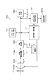
図1は、第1の実施形態に係る光電変換装置の概略構成を表すブロック図である。光電変換装置は、光を検出し信号を出力するユニットセルを有する。本実施形態の光電変換装置は、撮像可能な光電変換装置とし、ユニットセルを画素とする。本実施形態に係る光電変換装置は撮像を行わない装置であっても効果を得ることができる。撮像を行わない装置としては、例えば、測距センサ、測光センサなどがある。測距センサは、典型的には被写体までの距離情報を生成するために用いられるセンサであり、例えばTOF(Time Of Flight)センサ等が有る。測光センサは、典型的には被写体の明るさを検出するために用いられるセンサである。
(First Embodiment)
FIG. 1 is a block diagram showing a schematic configuration of a photoelectric conversion device according to a first embodiment. The photoelectric conversion device has a unit cell that detects light and outputs a signal. The photoelectric conversion device of the present embodiment is a photoelectric conversion device capable of imaging, and the unit cell is a pixel. The photoelectric conversion device according to the present embodiment can be effective even if it is a device that does not perform imaging. Devices that do not perform imaging include, for example, a distance measuring sensor and a photometric sensor. The distance measuring sensor is typically a sensor used to generate distance information to a subject, and includes, for example, a TOF (Time Of Flight) sensor and the like. A photometric sensor is typically a sensor used to detect the brightness of a subject.
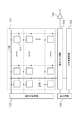
図1の光電変換装置は画素アレイ部101、垂直走査回路102、読み出し回路103、水平走査回路104、出力回路105、制御回路106を備える。
The photoelectric conversion device of FIG. 1 includes a
画素アレイ部101は、行方向及び列方向に配置された複数の画素107を備えている。画素アレイ部101には、撮像信号を検出する画素のほかに、遮光されたオプティカルブラック画素や信号を出力しないダミー画素が配置されていてもよい。
The
垂直走査回路102は画素107内のトランジスタのオン(導通状態)またはオフ(非導通状態)を切り替えるための制御信号を供給する。制御信号を供給する制御信号線108が、各画素行に対応して配されている。1つの制御信号線108には1つの画素行に配された複数の画素107が接続されている。
The
垂直走査回路102は、制御回路106からの信号を受けて、各画素行に配された複数の画素107に制御信号を共有する。
The
読み出し回路103は垂直出力線208に出力された画素信号に対して、増幅処理やAD変換処理などの信号処理を実施する。読み出し回路103は、画素107のリセット時の信号および光電変換時の信号に基づく相関二重サンプリング処理などを行う。
The
水平走査回路104は、読み出し回路103に制御信号を供給する。水平走査回路104は、制御信号を読み出し回路103に供給する。水平走査回路104からの制御信号によって、読み出し回路103で処理された画素信号を出力回路105に転送する。出力回路105は、信号を光電変換装置の外部の信号処理部に出力する。制御回路106は、タイミングジェネレーターなどの、各回路を制御するための回路である。制御回路106は、垂直走査回路102、読み出し回路103、水平走査回路104、及び出力回路105の動作やそのタイミングを制御する制御信号を供給する。垂直走査回路102、読み出し回路103、水平走査回路104、及び出力回路105への制御信号の少なくとも一部は、制御回路106ではなく光電変換装置の外部から供給してもよい。
The
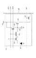
図2は、本実施形態における光電変換装置の画素107に関する模式的な回路図である。図2では、1つの画素107の構成を示しており、他の画素は省略している。
FIG. 2 is a schematic circuit diagram relating to the
図2において、画素107は、光電変換部201、第1転送トランジスタ202、第2転送トランジスタ203、増幅トランジスタ206、フローティングディフュージョン(FD)部204、リセットトランジスタ205、選択トランジスタ207を備える。FD部204は、増幅トランジスタ206の入力ノードである。各トランジスタは、例えばMOSFETにより構成され、平面視で、ドレインとソースの間には制御電極としてゲートを有する。
In FIG. 2, the
光電変換部201は、例えばフォトダイオードであるが、有機材料の光電変換膜やフォトゲート等の任意の構成が適用できる。増幅トランジスタ206は、入力ノードの電位に基づく信号を選択トランジスタ207へと出力する。増幅トランジスタ206の一端は、例えば、電源電圧VDDに接続される。増幅トランジスタ206はソースフォロワ回路の一部であり、増幅トランジスタ206のゲートが入力ノードである。光電変換部201と入力ノードとは、第1転送トランジスタ202と第2転送トランジスタ203とを介して接続されている。第1転送トランジスタ202は、光電変換部201からの電荷の転送を制御している。第2転送トランジスタ203の一端は第1転送トランジスタ202に接続され、他端は入力ノードと接続されている。第2転送トランジスタ203は、光電変換部201からの電荷の転送を制御するとともに、入力ノードの容量値を制御している。選択トランジスタ207は、増幅トランジスタ206と垂直出力線208との間を選択的に接続する。そして、選択トランジスタ207は、垂直走査回路からの制御信号のタイミングに合わせて増幅トランジスタ206からの信号を垂直出力線208へと出力する。リセットトランジスタ205は、入力ノードに接続されており、入力ノードをリセット電位に設定する(リセットする)ことができる。
The
第1転送トランジスタ202と第2転送トランジスタ203がオンになり光電変換部201からFD部204に電荷が転送されると、FD部204の電荷量に対応した画素信号電圧が増幅トランジスタ206のソースに出力される。
When the
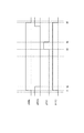
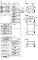
ここで、図3を参照しながら、第2転送トランジスタ203によるFD部204の容量値の制御について説明する。図3(a)は、光電変換部201、第1転送トランジスタ202、第2転送トランジスタ203を通る概略断面図である。図3(b)は、第1転送トランジスタ202と第2転送トランジスタ203とがオフのポテンシャルの概念図である。図3(c)は、第1転送トランジスタ202がオフであり、第2転送トランジスタ203がオンのポテンシャルの概念図である。
Here, the control of the capacitance value of the
図3(a)に示すように、半導体基板には、光電変換部201を構成するN型半導体領域(第1半導体領域)と、FD部の一部を構成するN型半導体領域(第2半導体領域)210と、N型半導体領域211が配されている。N型半導体領域210は、平面視で、第2転送トランジスタ203とリセットトランジスタのゲートとの間に形成されており、FD部の一部を構成する。N型半導体領域211は、平面視で、第1転送トランジスタ202のゲートと第2転送トランジスタ203のゲートとの間に形成されている
図3(b)及び図3(c)からわかるように、第2転送トランジスタ203をオンにする場合のFD部204の容量値は、第2転送トランジスタ203をオフにする場合のFD部204の容量値よりも大きい。第2転送トランジスタ203をオンにすることにより、第2転送トランジスタ203のゲート下にチャネルが形成され、N型半導体領域211とN型半導体領域210とが電気的に接続され、FD部204の容量値が大きくなる。したがって、光電変換部201からFD部204に電荷が転送されるときに、第2転送トランジスタ203をオンのままにしておくと、FD部204で保持可能な電荷量が増える。すなわち、FD部204の容量値が大きくなる。したがって、増幅トランジスタ206から出力される画素信号電圧が小さくなり、ダイナミックレンジの拡大が可能となる。一方で、光電変換部201からFD部204に電荷が転送されるときに、第2転送トランジスタ203をオフにしておくと、FD部204には容量が付加されない。つまり、FD部204の容量はFD部204自体が有する容量値から変化しない。したがって、FD部204で保持可能な電荷量が少ない。すなわち、FD部204の容量値が小さくなる。したがって、増幅トランジスタ206から出力される画素信号電圧が大きくなる。この場合には、FD部204の1つの電荷に対する電圧変化量(電荷電圧変換効率)を高めることができる。電荷電圧変換効率が高いとは、感度が高いとも言える。したがって、第2転送トランジスタ203のオンオフを制御することにより、FD部204の容量値を変えることができ、感度の切り替えを行うことができる。
As shown in FIG. 3A, the semiconductor substrate includes an N-type semiconductor region (first semiconductor region) constituting the
図3(b)及び図3(c)に示すように、FD部204の容量は、光電変換部201の容量よりも小さい。本実施形態によれば、第2転送トランジスタにより、FD部に容量を付加することができる。このため、FD部204自体の容量を大きくし、ダイナミックレンジを拡大することが可能となる。
As shown in FIGS. 3 (b) and 3 (c), the capacity of the
図4は、本実施形態に係る画素107の模式的な平面図である。図2の回路と対応する部分には同一の符号が付されており、既に説明した構成及び機能については説明を省略することもある。図3(a)の断面図は、図4のA−A’断面図に相当する。図4では、光電変換部201、画素107に含まれる各トランジスタのゲート、及び配線を導通させるためのコンタクトを示している。光電変換部201と各トランジスタのソースおよびドレインとは、シリコン(Si)などの半導体基板の内部に形成される。また、各トランジスタのゲートは、半導体基板の第1面側に形成されている。
FIG. 4 is a schematic plan view of the
図4に示すように、光電変換部201、第1転送トランジスタ202、第2転送トランジスタ203、FD部204、リセットトランジスタ205は直列に接続されている。これにより、入力ノードのリセット性能の低下を抑制しながら、光電変換装置のダイナミックレンジを拡大することができる。
As shown in FIG. 4, the
比較例として、FD部、FD部への容量付加を制御する制御トランジスタ、リセットトランジスタが直列に配されている場合について説明する。リセットトランジスタの一端が制御トランジスタに接続され、リセットトランジスタの他端に電源電圧VDDが接続される。比較例では、FD部をリセットする際に、リセットトランジスタのゲート及び制御トランジスタのゲートを介して電源電圧VDDの電位がFD部204に供給されることになる。この場合は、トランジスタのソースとドレインとを結ぶ方向における長さ(ゲート長)が、リセットトランジスタのゲートのみの場合と比較して長くなりやすい。ゲート長が長くなるとチャネル抵抗が大きくなるため、リセット性能の低下が生じる可能性がある。リセット性能の低下とは、例えば、リセットレベルの静定時間が伸びてしまうことや、各画素のリセット電位のばらつきが生じやすくなることを意味している。リセットトランジスタのゲート長と制御トランジスタのゲート長を短くすることにより、リセット性能の低下を防げる可能性はあるものの、FD部への容量付加を制御できなくなる可能性がある。したがって、比較例では一般的にゲート長を短くしにくく、チャネル抵抗によりリセット性能の低下が生じる可能性がある。
As a comparative example, a case where the FD unit, the control transistor for controlling the capacitance addition to the FD unit, and the reset transistor are arranged in series will be described. One end of the reset transistor is connected to the control transistor, and the power supply voltage VDD is connected to the other end of the reset transistor. In the comparative example, when the FD unit is reset, the potential of the power supply voltage VDD is supplied to the
これに対して、本実施形態では、上述の通り、FD部204とリセットトランジスタ205を、FD部204の容量値を制御する第2転送トランジスタ203を介することなく直列に接続している。例えば、リセットトランジスタのソースまたはドレインの一方がFD部204の一部を構成する。したがって、比較例に比して、リセット電位が供給される際のチャネル抵抗を減らすことができ、入力ノードのリセット性能の低下を抑制することができる。
On the other hand, in the present embodiment, as described above, the
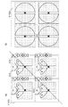
図5(a)及び図5(b)は、図2の画素107における各トランジスタの制御信号を示すタイミング図である。タイミング図の横軸は時間である。図5(a)及び図5(b)において、図2で示した各制御信号pSEL、pRES、pTX1、pTX2の電位の状態が示されている。pSELは、選択トランジスタを制御する信号であり、pRESはリセットトランジスタを制御する信号であり、pTX1は第1転送トランジスタを制御する信号であり、pTX2は第2転送トランジスタを制御する信号である。図5(a)は、低FD容量で読み出す場合のタイミングであり、図5(b)は、高FD容量で読み出す場合のタイミングである。また、図6(a)〜(e)は図5(a)のそれぞれのタイミングにおけるポテンシャル図であり、図6(f)〜(h)は図5(b)のそれぞれのタイミングにおけるポテンシャル図である。
5 (a) and 5 (b) are timing diagrams showing control signals of each transistor in
まず、図5(a)及び図6(a)〜(e)を参照しながら、低FD容量で読み出す場合の駆動について説明する。 First, the drive in the case of reading with a low FD capacitance will be described with reference to FIGS. 5 (a) and 6 (a) to 6 (e).
まず、時刻t1において、pSELをHiレベル(以下Hi)にして読み出し行の画素の選択トランジスタをオンする。時刻t2において、pRESをHiからLowレベル(以下Lo)にしてリセットトランジスタをオンからオフへと切り替える。このとき、第2転送トランジスタはオフになっている。第1転送トランジスタおよび第2転送トランジスタがオフの状態において、光電変換部は信号電荷を蓄積する。この状態におけるポテンシャル図を図6(a)に示す。この状態においてFD部は低FD容量時のリセットレベルにあり、増幅トランジスタ206はその電位を読み出してリセット信号(N信号)として垂直信号線に出力する。時刻t3までは、光電変換部における電荷の蓄積期間ともいえる。
First, at time t1, the pSEL is set to the Hi level (hereinafter, Hi) and the selection transistor of the pixel in the read row is turned on. At time t2, the pRES is changed from Hi to Low level (hereinafter Lo) and the reset transistor is switched from on to off. At this time, the second transfer transistor is turned off. When the first transfer transistor and the second transfer transistor are off, the photoelectric conversion unit accumulates signal charges. The potential diagram in this state is shown in FIG. 6 (a). In this state, the FD unit is at the reset level when the FD capacitance is low, and the
時刻t3に、pTX1をHiにして第1転送トランジスタをオンする。時刻t3に、光電変換部からFD部への読み出し動作が開始される。この状態におけるポテンシャル図を図6(b)に示す。図6(b)に示すように、光電変換部で蓄積された電荷が第1転送トランジスタのゲート下に移動する。 At time t3, pTX1 is set to Hi and the first transfer transistor is turned on. At time t3, the reading operation from the photoelectric conversion unit to the FD unit is started. The potential diagram in this state is shown in FIG. 6 (b). As shown in FIG. 6B, the electric charge accumulated in the photoelectric conversion unit moves under the gate of the first transfer transistor.
第1転送トランジスタをオンにした状態のまま、時刻t4に、pTX2をHiにして第2転送トランジスタをオンにする。この状態におけるポテンシャル図を図6(c)に示す。図6(c)に示すように、光電変換部で蓄積された電荷は、第1転送トランジスタおよび第2転送トランジスタをオンすることにより容量が付加されたFD部へと転送される。 With the first transfer transistor turned on, at time t4, pTX2 is set to Hi and the second transfer transistor is turned on. The potential diagram in this state is shown in FIG. 6 (c). As shown in FIG. 6C, the electric charge accumulated in the photoelectric conversion unit is transferred to the FD unit to which the capacitance is added by turning on the first transfer transistor and the second transfer transistor.
時刻t5に、pTX1をHiからLoにして第1転送トランジスタをオフする。この状態におけるポテンシャル図を図6(d)に示す。図6(d)に示すように、光電変換部とFD部との間にポテンシャルバリアが形成される。これにより、信号電荷は、第2転送トランジスタをオンすることにより容量が付加されたFD部へと転送される。 At time t5, pTX1 is changed from Hi to Lo and the first transfer transistor is turned off. The potential diagram in this state is shown in FIG. 6 (d). As shown in FIG. 6D, a potential barrier is formed between the photoelectric conversion section and the FD section. As a result, the signal charge is transferred to the FD unit to which the capacitance is added by turning on the second transfer transistor.
時刻t6に、pTX2をHiからLoにして第2転送トランジスタをオフする。この状態におけるポテンシャルバリア図を図6(e)に示す。図6(e)に示すように、図6(d)に比べて第2転送トランジスタのゲート下のポテンシャルが高くなり、第2転送トランジスタによる容量が付加されていないFD部のみに信号電荷が保持される。 At time t6, pTX2 is changed from Hi to Lo and the second transfer transistor is turned off. The potential barrier diagram in this state is shown in FIG. 6 (e). As shown in FIG. 6 (e), the potential under the gate of the second transfer transistor is higher than that in FIG. 6 (d), and the signal charge is retained only in the FD portion to which the capacitance by the second transfer transistor is not added. Will be done.
その後、増幅トランジスタがFD部の電位に応じた信号(S信号)を出力する。 After that, the amplification transistor outputs a signal (S signal) corresponding to the potential of the FD unit.
なお、図5(a)では、第1の転送トランジスタと第2の転送トランジスタをオンするタイミングとオフするタイミングとをずらしている。具体的には、第1転送トランジスタをオンした後に第2転送トランジスタをオンし、第1転送トランジスタをオフした後に第2転送トランジスタをオフしている。これにより、第1転送トランジスタと第2転送トランジスタとのオンオフ制御のタイミングにずれが生じても、光電変換部で蓄積された信号電荷が光電変換部に残ることを抑制しやすくなる。第1転送トランジスタと第2転送トランジスタとのオン/オフのタイミングは図5(a)に示すタイミングに限定されない。例えば、第1転送トランジスタと第2転送トランジスタとでオン/オフのタイミングを同じにしてもよい。また、第2転送トランジスタをオンした後に、第1転送トランジスタをオンし、第1転送トランジスタをオフした後に、第2転送トランジスタをオフしてもよい。 In FIG. 5A, the timing of turning on the first transfer transistor and the timing of turning off the second transfer transistor are staggered. Specifically, the second transfer transistor is turned on after the first transfer transistor is turned on, and the second transfer transistor is turned off after the first transfer transistor is turned off. As a result, even if the on / off control timing of the first transfer transistor and the second transfer transistor is deviated, it becomes easy to prevent the signal charge accumulated in the photoelectric conversion unit from remaining in the photoelectric conversion unit. The on / off timing of the first transfer transistor and the second transfer transistor is not limited to the timing shown in FIG. 5A. For example, the on / off timing may be the same for the first transfer transistor and the second transfer transistor. Further, the second transfer transistor may be turned on after the second transfer transistor is turned on, the first transfer transistor may be turned on, the first transfer transistor may be turned off, and then the second transfer transistor may be turned off.
続いて、図5(b)及び図6(f)〜(h)を参照しながら、高FD容量で読み出す場合の駆動について説明する。 Subsequently, the drive in the case of reading with a high FD capacitance will be described with reference to FIGS. 5 (b) and 6 (f) to 6 (h).
時刻t1に、pSELをHiにして読み出し行の画素の選択トランジスタをオンする。時刻t2に、pRESをHiからLoにしてリセットリセットトランジスタをオンからオフへと切り替える。このとき、第2転送トランジスタはオンになっている。この状態におけるポテンシャル図を図6(f)に示す。図6(f)に示すように、第2転送トランジスタをオンすることによりFD部に容量が付加され、図6(a)の場合と比べてFD容量が大きくなっている。このようにFD部に容量が付加された状態でリセット動作を行う。この状態においてFDは高FD容量時のリセットレベルにあり、その信号を読み出してN信号とする。高FD容量で読み出す場合は、例えば、光電変換部への入射光量が低FD容量で読み出す場合に比べて多い場合が想定される。したがって、光電変換部に蓄積される信号電荷は、低FD容量で読み出す場合に比べて多くなっている。例えば、光電変換部に蓄積される信号電荷量が、容量が付加されていないFD容量に比べて多くなっている。 At time t1, pSEL is set to Hi and the selection transistor of the pixel in the read row is turned on. At time t2, the pRES is changed from Hi to Lo and the reset reset transistor is switched from on to off. At this time, the second transfer transistor is on. The potential diagram in this state is shown in FIG. 6 (f). As shown in FIG. 6 (f), a capacitance is added to the FD portion by turning on the second transfer transistor, and the FD capacitance is larger than that in the case of FIG. 6 (a). In this way, the reset operation is performed with the capacity added to the FD unit. In this state, the FD is at the reset level at the time of high FD capacitance, and the signal is read out and used as an N signal. When reading with a high FD capacitance, for example, it is assumed that the amount of incident light on the photoelectric conversion unit is larger than when reading with a low FD capacitance. Therefore, the signal charge accumulated in the photoelectric conversion unit is larger than that in the case of reading with a low FD capacitance. For example, the amount of signal charge stored in the photoelectric conversion unit is larger than that of the FD capacitance to which no capacitance is added.
時刻t3に、pTX1をHiにして第1転送トランジスタをオンにする。このとき第2転送トランジスタは、pTX2がHiであり、オンしている。この状態におけるポテンシャル図を図6(g)に示す。図6(g)に示すように、光電変換部で蓄積された信号電荷が、容量が付加されたFD部に転送される。 At time t3, pTX1 is set to Hi and the first transfer transistor is turned on. At this time, the second transfer transistor has pTX2 Hi and is on. The potential diagram in this state is shown in FIG. 6 (g). As shown in FIG. 6 (g), the signal charge accumulated in the photoelectric conversion unit is transferred to the FD unit to which the capacitance is added.
時刻t4に、pTX1をHiからLoにして第1転送トランジスタをオフにする。このとき第2転送トランジスタは、pTX2がHiの状態を維持しており、オンしたままである。この状態におけるポテンシャル図を図6(h)に示す。図6(h)に示すように、FD部に容量を付加したままで光電変換部とFD部との間にポテンシャルバリアが形成される。 At time t4, pTX1 is changed from Hi to Lo and the first transfer transistor is turned off. At this time, the second transfer transistor keeps the pTX2 in the Hi state and remains on. The potential diagram in this state is shown in FIG. 6 (h). As shown in FIG. 6 (h), a potential barrier is formed between the photoelectric conversion unit and the FD unit while the capacitance is added to the FD unit.
その後、第2転送トランジスタをオンしたままの状態で増幅トランジスタがFD部の電位に応じた信号(S信号)を出力する。 After that, the amplification transistor outputs a signal (S signal) corresponding to the potential of the FD unit with the second transfer transistor turned on.
なお、図5(b)では、第2転送トランジスタは、光電変換部の蓄積動作期間および信号読み出し動作期間にわたってオンしたままの状態を維持しているが、これに限定されない。第2転送トランジスタは、少なくともN信号を読み出す期間とS信号を読み出す期間においてオンしていればよい。例えば、N信号を読み出した後に、時刻t2で第2転送トランジスタをオフし、時刻t3の第1転送トランジスタがオンするタイミングと同じタイミングで第2転送トランジスタをオンしてもよい。 In FIG. 5B, the second transfer transistor is maintained in the ON state for the accumulation operation period and the signal reading operation period of the photoelectric conversion unit, but is not limited to this. The second transfer transistor may be turned on at least during the period for reading the N signal and the period for reading the S signal. For example, after reading the N signal, the second transfer transistor may be turned off at time t2, and the second transfer transistor may be turned on at the same timing as when the first transfer transistor at time t3 is turned on.
図5(a)及び図5(b)に示すような駆動によれば、光電変換部への入射光量に応じてFD容量を変えることができる。例えば、光電変換部への入射光量が第1の光量である場合(低輝度の被写体を撮像する場合)は、第2転送トランジスタをオフにした状態で増幅トランジスタは信号を出力する低FD容量の読み出し駆動を採用する。一方で、光電変換部への入射光量が第1の光量よりも多い第2光量である場合(高輝度の被写体を撮像する場合)は、第2転送トランジスタをオンにした状態で増幅トランジスタは信号を出力する高FD容量の読み出し駆動を採用する。信号電荷量が少ない場合は、低FD容量の読み出し駆動を採用することにより、高FD容量の場合に比べて、低ノイズで高感度な信号を読み出すことができる。一方で、信号電荷量が多い場合は、高FD容量の読み出し駆動を採用することにより、低FD容量の場合に比べて、高飽和な信号を読み出すことができる。したがって、光電変換装置のダイナミックレンジを拡大することできる。 According to the drive as shown in FIGS. 5 (a) and 5 (b), the FD capacitance can be changed according to the amount of light incident on the photoelectric conversion unit. For example, when the amount of light incident on the photoelectric conversion unit is the first amount of light (when imaging a low-luminance subject), the amplification transistor has a low FD capacitance that outputs a signal with the second transfer transistor turned off. Uses read drive. On the other hand, when the amount of light incident on the photoelectric conversion unit is the second amount of light that is larger than the amount of the first light (when capturing a high-luminance subject), the amplification transistor signals with the second transfer transistor turned on. A high FD capacitance read drive that outputs When the amount of signal charge is small, by adopting the read drive with a low FD capacitance, it is possible to read a signal with low noise and high sensitivity as compared with the case with a high FD capacitance. On the other hand, when the amount of signal charge is large, by adopting the read drive of high FD capacitance, it is possible to read out a highly saturated signal as compared with the case of low FD capacitance. Therefore, the dynamic range of the photoelectric conversion device can be expanded.
図2では、画素107が選択トランジスタ207を含むが、選択トランジスタ207は必須の構成ではない。画素107が選択トランジスタ207を含まない場合において、増幅トランジスタ206は、FD部204の電位に基づく信号を、選択トランジスタ207を介することなく、垂直出力線208へと出力する。
In FIG. 2, the
(第2の実施形態)
次に、第2の実施形態に係る光電変換装置について、図7を参照しながら説明する。以下の説明では、主として第1の実施形態と異なる点について説明する。
(Second Embodiment)
Next, the photoelectric conversion device according to the second embodiment will be described with reference to FIG. 7. In the following description, the points different from the first embodiment will be mainly described.
本実施形態は、高FD容量の読み出し駆動における駆動タイミングが異なる。具体的には、選択トランジスタをオンしている画素行(第1の画素行)では第2転送トランジスタをオンし、選択トランジスタをオフしている画素行(第2の画素行)では第2転送トランジスタをオフしている。第2転送トランジスタのオンするタイミングとオフするタイミングとは、選択トランジスタがオンするタイミングとオフするタイミングと一致している。具体的には、時刻t1で選択トランジスタと第2転送トランジスタがオンし、時刻t5で選択トランジスタと第2転送トランジスタがオフしている。 In this embodiment, the drive timing in the read drive with a high FD capacitance is different. Specifically, the second transfer transistor is turned on in the pixel row (first pixel row) in which the selection transistor is turned on, and the second transfer is performed in the pixel row (second pixel row) in which the selection transistor is turned off. The transistor is off. The timing of turning on and the timing of turning off the second transfer transistor coincides with the timing of turning on and the timing of turning off the selected transistor. Specifically, the selection transistor and the second transfer transistor are turned on at time t1, and the selection transistor and the second transfer transistor are turned off at time t5.
本実施形態によれば、光電変換装置のダイナミックレンジを拡大することを可能にしつつ、選択トランジスタをオフしている画素行に配された画素において光電変換部からFD部へのパンチスルーを抑制することができる。 According to the present embodiment, while making it possible to expand the dynamic range of the photoelectric conversion device, punch-through from the photoelectric conversion unit to the FD unit is suppressed in the pixels arranged in the pixel row in which the selection transistor is turned off. be able to.
(第3の実施形態)
次に、第3の実施形態に係る光電変換装置について、図8及び図9を参照しながら説明する。図8は、本実施形態における画素の平面図であり、図9は本実施形態に係る画素の回路図である。以下の説明では、主として、第1の実施形態と異なる点について説明する。
(Third Embodiment)
Next, the photoelectric conversion device according to the third embodiment will be described with reference to FIGS. 8 and 9. FIG. 8 is a plan view of the pixels in the present embodiment, and FIG. 9 is a circuit diagram of the pixels according to the present embodiment. In the following description, the points different from the first embodiment will be mainly described.
本実施形態は、第1の光電変換部201aと第2の光電変換部201bで第2転送トランジスタ203、FD部204、リセットトランジスタ205、増幅トランジスタ206、選択トランジスタ207を共有する。第1の光電変換部201aと第2転送トランジスタ203とは、第1転送トランジスタ202a(第1の第1転送トランジスタ)を介して接続される。第2の光電変換部201bと第2転送トランジスタ203とは、第1転送トランジスタ202b(第2の第1転送トランジスタ)を介して接続される。
In this embodiment, the first
本実施形態によれば、1つの第2転送トランジスタ203のゲートとFD部204とが接する。したがって、複数の第1転送トランジスタがFD部に接する場合に比べて、FDに接するゲート容量を減らすことができ、FD容量を減らすことができる。
According to this embodiment, the gate of one
(第4の実施形態)
次に、第4の実施形態に係る子電変換装置について、図10および図11を参照しながら説明する。図10は、光電変換装置1100の分解斜視図である。図10は、本実施形態における画素の平面図である。図11(a)は、半導体基板のトランジスタが形成される側の面(第1面)1110Aから視た平面図である。図11(b)は、半導体基板の第1面に対向する面(第2面)1110Bから視た平面図である。以下では、第3の実施形態と異なる点について説明する。
(Fourth Embodiment)
Next, the child electric conversion device according to the fourth embodiment will be described with reference to FIGS. 10 and 11. FIG. 10 is an exploded perspective view of the
本実施形態に係る光電変換装置は、第2面1110Bの側から光が入射する、いわゆる裏面照射型の光電変換装置である。図10に示すように、1つの半導体基板1110に画素アレイ部101が設けられている。別の半導体基板1120には、制御部1121と信号処理部1122が設けられている。制御部1121と信号処理部1122のそれぞれの半導体基板1110への正射影は、少なくとも一部が画素アレイ部101と重畳している。本実施形態の光電変換装置1100は、さらに、別の処理回路を含む半導体基板を有していてもよく、3つ以上の半導体基板が積層されていてもよい。
The photoelectric conversion device according to the present embodiment is a so-called back-illuminated photoelectric conversion device in which light is incident from the side of the
制御部1121は、画素に含まれるトランジスタに制御信号を供給する垂直走査回路や、電源回路を含み得る。また、制御部1121は光電変換装置を駆動するためのタイミング発生回路や、変換回路へ参照信号を供給する参照信号供給回路、増幅回路あるいは変換回路から信号を順次読み出すための水平走査回路を含み得る。例えば、制御部1121は、図1における光電変換装置の垂直走査回路102、水平走査回路104、制御回路106などを含む。
The
信号処理部1122は、画素領域で発生した信号電荷に基づく電気信号を処理する。信号処理部1122は、ノイズ除去回路、増幅回路、変換回路、画像信号処理回路を含むことができる。ノイズ除去回路は、例えば相関二重サンプリング(CDS)回路である。増幅回路は、例えば列アンプ回路である。変換回路は、例えばコンパレータとカウンタで構成されたアナログデジタル変換(ADC)回路である。画像信号処理回路は、例えばメモリとプロセッサを含み、アナログデジタル変換されたデジタル信号から画像データを生成したり、画像データに画像処理を施したりする。例えば、信号処理部1122は、図1における読み出し回路103を含む。
The
図11(a)および図11(b)に、平面視におけるマイクロレンズの光学中心1001を示す。ユニットセルは2つの光電変換部を含む。ここで述べているユニットセルとは、1つの光学中心に対応する光電変換部及び光電変換部からの読み出し回路をひとまとまりとしてユニットセルと定義している。例えば、図11では、ユニットセルは、平面視でマイクロレンズに重なる2つの光電変換部、各光電変換部から電荷の転送を制御する第1転送トランジスタ、第2転送トランジスタ、増幅トランジスタ、及び、リセットトランジスタにより構成される。
11 (a) and 11 (b) show the
図11(a)に示すように、第2転送トランジスタ203に接続されているFD部204は、ユニットセル内において、光学中心1001に対して最も遠い位置に配されている。例えば、FD部204は、ユニットセル内の角に形成されている。上述の通り、裏面照射型の光電変換装置の場合、光が裏面から入射する。したがって、FD部204が光学中心1001に近い場合、光電変換部で光電変換された信号電荷がFD部へ流入する確率が上がり、感度低下や感度の入射角特性の非対称性を生じさせる可能性がある。
As shown in FIG. 11A, the
第2転送トランジスタを持たない比較例では、複数の光電変換部がFD部を共有する場合には、FD部が第1転送トランジスタの一部を構成するため、FD部の平面的な配置に大きな制約が生じていた。これに対して、本実施形態によれば、第2転送トランジスタを付加することで複数の光電変換部がFD部を共有する場合でもFD部をより高い自由度で配置することが可能となる。 In the comparative example not having the second transfer transistor, when a plurality of photoelectric conversion units share the FD unit, the FD unit forms a part of the first transfer transistor, which is large in the planar arrangement of the FD unit. There were restrictions. On the other hand, according to the present embodiment, by adding the second transfer transistor, the FD unit can be arranged with a higher degree of freedom even when a plurality of photoelectric conversion units share the FD unit.
(第5の実施形態)
図12は、本実施形態に係る光電変換システム1200の構成を示すブロック図である。本実施形態の光電変換システム1200は、光電変換装置1204を含む。ここで、光電変換装置1204は、上述の実施形態で述べた光電変換装置のいずれかを適用することができる。光電変換システム1200は例えば、撮像システムとして用いることができる。光電変換システム1200の具体例としては、デジタルスチルカメラ、デジタルカムコーダー、監視カメラ等が挙げられる。図12では、光電変換システム1200としてデジタルスチルカメラの例を示している。
(Fifth Embodiment)
FIG. 12 is a block diagram showing the configuration of the
図12に示す光電変換システム1200は、光電変換装置1204、被写体の光学像を光電変換装置1204に結像させるレンズ1202、レンズ1202を通過する光量を可変にするための絞り1203、レンズ1202の保護のためのバリア1201を有する。レンズ1202および絞り1203は、光電変換装置1204に光を集光する光学系である。
The
光電変換システム1200は、光電変換装置1204から出力される出力信号の処理を行う信号処理部1205を有する。信号処理部1205は、必要に応じて入力信号に対して各種の補正、圧縮を行って出力する信号処理の動作を行う。光電変換システム1200は、更に、画像データを一時的に記憶するためのバッファメモリ部1206、外部コンピュータ等と通信するための外部インターフェース部(外部I/F部)1209を有する。更に光電変換システム1200は、撮像データの記録又は読み出しを行うための半導体メモリ等の記録媒体1211、記録媒体1211に記録または読み出しを行うための記録媒体制御インターフェース部(記録媒体制御I/F部)1210を有する。記録媒体1211は、光電変換システム1200に内蔵されていてもよく、着脱可能であってもよい。また、記録媒体制御I/F部1210から記録媒体1211との通信や外部I/F部1209からの通信は無線によってなされてもよい。
The
更に光電変換システム1200は、各種演算を行うとともにデジタルスチルカメラ全体を制御する全体制御・演算部1208、光電変換装置1204と信号処理部1205に各種タイミング信号を出力するタイミング発生部1207を有する。ここで、タイミング信号などは外部から入力されてもよく、光電変換システム1200は、少なくとも光電変換装置1204と、光電変換装置1204から出力された出力信号を処理する信号処理部1205とを有すればよい。第4の実施形態にて説明したようにタイミング発生部1207は光電変換装置に搭載されていてもよい。全体制御・演算部1208およびタイミング発生部1207は、光電変換装置1204の制御機能の一部または全部を実施するように構成してもよい。
Further, the
光電変換装置1204は、画像用信号を信号処理部1205に出力する。信号処理部1205は、光電変換装置1204から出力される画像用信号に対して所定の信号処理を実施し、画像データを出力する。また、信号処理部1205は、画像用信号を用いて、画像を生成する。なお、信号処理部1205やタイミング発生部1207は、光電変換装置に搭載されていてもよい。つまり、信号処理部1205やタイミング発生部1207は、画素が配された基板に設けられていてもよく、第3の実施形態に記載したような別の基板に設けられている構成であってもよい。上述した各実施形態の光電変換装置を用いて撮像システムを構成することにより、より良質の画像が取得可能な撮像システムを実現することができる。
The
(第6の実施形態)
本実施形態の光電変換システム及び移動体について、図13よび図14を用いて説明する。図13は、本実施形態による光電変換システム及び移動体の構成例を示す概略図である。図14は、本実施形態による光電変換システムの動作を示すフロー図である。本実施形態では、光電変換システムとして、車載カメラの一例を示す。
(Sixth Embodiment)
The photoelectric conversion system and the moving body of the present embodiment will be described with reference to FIGS. 13 and 14. FIG. 13 is a schematic view showing a configuration example of a photoelectric conversion system and a mobile body according to the present embodiment. FIG. 14 is a flow chart showing the operation of the photoelectric conversion system according to the present embodiment. In this embodiment, an example of an in-vehicle camera is shown as a photoelectric conversion system.
図13は、車両システムとこれに搭載される撮像を行う光電変換システムの一例を示したものである。光電変換システム1301は、光電変換装置1302、画像前処理部1315、集積回路1303、光学系1314を含む。光学系1314は、光電変換装置1302に被写体の光学像を結像する。光電変換装置1302は、光学系1314により結像された被写体の光学像を電気信号に変換する。光電変換装置1302は、上述の各実施形態のいずれかの光電変換装置である。画像前処理部1315は、光電変換装置1302から出力された信号に対して所定の信号処理を行う。画像前処理部1315の機能は、光電変換装置1302内に組み込まれていてもよい。光電変換システム1301には、光学系1314、光電変換装置1302及び画像前処理部1315が、少なくとも2組設けられており、各組の画像前処理部1315からの出力が集積回路1303に入力されるようになっている。
FIG. 13 shows an example of a vehicle system and a photoelectric conversion system for imaging mounted on the vehicle system. The
集積回路1303は、撮像システム用途向けの集積回路であり、メモリ1305を含む画像処理部1304、光学測距部1306、視差演算部1307、物体認知部1308、異常検出部1309を含む。画像処理部1304は、画像前処理部1315の出力信号に対して、現像処理や欠陥補正等の画像処理を行う。メモリ1305は、撮像画像の一次記憶、撮像画素の欠陥位置を格納する。光学測距部1306は、被写体の合焦や、測距を行う。視差演算部1307は、複数の光電変換装置1302により取得された複数の画像データから視差情報(視差画像の位相差)の算出を行う。物体認知部1308は、車、道、標識、人等の被写体の認知を行う。異常検出部1309は、光電変換装置1302の異常を検出すると、主制御部1313に異常を発報する。
The
集積回路1303は、専用に設計されたハードウェアによって実現されてもよいし、ソフトウェアモジュールによって実現されてもよいし、これらの組合せによって実現されてもよい。また、FPGA(Field Programmable Gate Array)やASIC(Application Specific Integrated Circuit)等によって実現されてもよいし、これらの組合せによって実現されてもよい。
The
主制御部1313は、光電変換システム1301、車両センサ1310、制御ユニット1320等の動作を統括・制御する。主制御部1313を持たず、光電変換システム1301、車両センサ1310、制御ユニット1320が個別に通信インターフェースを有して、それぞれが通信ネットワークを介して制御信号の送受を行う(例えばCAN規格)方法も取り得る。
The
集積回路1303は、主制御部1313からの制御信号を受け或いは自身の制御部によって、光電変換装置1302へ制御信号や設定値を送信する機能を有する。
The
光電変換システム1301は、車両センサ1310に接続されており、車速、ヨーレート、舵角などの自車両走行状態及び自車外環境や他車・障害物の状態を検出することができる。車両センサ1310は、視差画像から対象物までの距離情報を取得する距離情報取得手段でもある。また、光電変換システム1301は、自動操舵、自動巡行、衝突防止機能等の種々の運転支援を行う運転支援制御部1311に接続されている。特に、衝突判定機能に関しては、光電変換システム1301や車両センサ1310の検出結果を基に他車・障害物との衝突推定・衝突有無を判定する。これにより、衝突が推定される場合の回避制御、衝突時の安全装置起動を行う。
The
また、光電変換システム1301は、衝突判定部での判定結果に基づいて、ドライバーに警報を発する警報装置1312にも接続されている。例えば、衝突判定部の判定結果として衝突可能性が高い場合、主制御部1313は、ブレーキをかける、アクセルを戻す、エンジン出力を抑制するなどして、衝突を回避、被害を軽減する車両制御を行う。警報装置1312は、音等の警報を鳴らす、カーナビゲーションシステムやメーターパネルなどの表示部画面に警報情報を表示する、シートベルトやステアリングに振動を与えるなどしてユーザに警告を行う。
The
本実施形態では、車両の周囲、例えば前方又は後方を光電変換システム1301で撮影する。図13(b)に、車両前方を光電変換システム1301で撮像する場合の光電変換システム1301の配置例を示す。
In the present embodiment, the periphery of the vehicle, for example, the front or the rear, is photographed by the
2つの光電変換装置1302は、車両1300の前方に配置される。具体的には、車両1300の進退方位又は外形(例えば車幅)に対する中心線を対称軸に見立て、その対称軸に対して2つの光電変換装置1302が線対称に配置されると、車両1300と被写対象物との間の距離情報の取得や衝突可能性の判定を行う上で好ましい。また、光電変換装置1302は、運転者が運転席から車両1300の外の状況を視認する際に運転者の視野を妨げない配置が好ましい。警報装置1312は、運転者の視野に入りやすい配置が好ましい。
The two
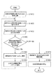
次に、光電変換システム1301における光電変換装置1302の故障検出動作について、図14を用いて説明する。光電変換装置1302の故障検出動作は、図14に示すステップS1410〜S1480に従って実施される。
Next, the failure detection operation of the
ステップS1410は、光電変換装置1302のスタートアップ時の設定を行うステップである。すなわち、光電変換システム1301の外部(例えば主制御部1313)又は光電変換システム1301の内部から、光電変換装置1302の動作のための設定を送信し、光電変換装置1302の撮像動作及び故障検出動作を開始する。
Step S1410 is a step of setting the
次いで、ステップS1420において、有効画素から画素信号を取得する。また、ステップS1430において、故障検出用に設けた故障検出画素からの出力値を取得する。この故障検出画素は、有効画素と同じく光電変換部を備える。この光電変換部には、所定の電圧が書き込まれる。故障検出用画素は、この光電変換部に書き込まれた電圧に対応する信号を出力する。なお、ステップS1420とステップS1430とは逆でもよい。 Next, in step S1420, a pixel signal is acquired from the effective pixel. Further, in step S1430, the output value from the failure detection pixel provided for failure detection is acquired. The failure detection pixel includes a photoelectric conversion unit like the effective pixel. A predetermined voltage is written in this photoelectric conversion unit. The failure detection pixel outputs a signal corresponding to the voltage written in the photoelectric conversion unit. The steps S1420 and S1430 may be reversed.
次いで、ステップS1440において、故障検出画素の出力期待値と、実際の故障検出画素からの出力値との該非判定を行う。ステップS1440における該非判定の結果、出力期待値と実際の出力値とが一致している場合は、ステップS1450に移行し、撮像動作が正常に行われていると判定し、処理ステップがステップS1460へと移行する。ステップS1460では、走査行の画素信号をメモリ1305に送信して一次保存する。そののち、ステップS1420に戻り、故障検出動作を継続する。一方、ステップS1440における該非判定の結果、出力期待値と実際の出力値とが一致していない場合は、処理ステップはステップS1470に移行する。ステップS1470において、撮像動作に異常があると判定し、主制御部1313、又は警報装置1312に警報を発報する。警報装置1312は、表示部に異常が検出されたことを表示させる。その後、ステップS1480において光電変換装置1302を停止し、光電変換システム1301の動作を終了する。
Next, in step S1440, the non-determination of the expected output value of the failure detection pixel and the output value from the actual failure detection pixel is performed. If the expected output value and the actual output value match as a result of the non-determination in step S1440, the process proceeds to step S1450, it is determined that the imaging operation is normally performed, and the processing step proceeds to step S1460. And migrate. In step S1460, the pixel signal of the scanning line is transmitted to the
なお、本実施形態では、1行毎にフローチャートをループさせる例を例示したが、複数行毎にフローチャートをループさせてもよいし、1フレーム毎に故障検出動作を行ってもよい。ステップS1470の警報の発報は、無線ネットワークを介して、車両の外部に通知するようにしてもよい。 In the present embodiment, an example of looping the flowchart for each line has been illustrated, but the flowchart may be looped for each of a plurality of lines, or the failure detection operation may be performed for each frame. The alarm issued in step S1470 may be notified to the outside of the vehicle via the wireless network.
また、本実施形態では、他の車両と衝突しない制御を説明したが、他の車両に追従して自動運転する制御や、車線からはみ出さないように自動運転する制御などにも適用可能である。さらに、光電変換システム1301は、自車両等の車両に限らず、例えば、船舶、航空機或いは産業用ロボットなどの移動体(移動装置)に適用することができる。加えて、移動体に限らず、高度道路交通システム(ITS)等、広く物体認識を利用する機器に適用することができる。
Further, in the present embodiment, the control that does not collide with other vehicles has been described, but it can also be applied to the control that automatically drives following other vehicles and the control that automatically drives so as not to go out of the lane. .. Further, the
本発明の光電変換装置は、更に、カラーフィルタやマイクロレンズを有する構成であってもよく、距離情報など各種情報を取得可能な構成であってもよい。また、増幅トランジスタはソースフォロワ回路の一部であるが、AD変換器の一部を構成していてもよい。具体的には、AD変換器が含む比較器の一部を増幅トランジスタが構成していてもよい。また、比較器の一部の構成が別の半導体基板に設けられている構成であってもよい。 The photoelectric conversion device of the present invention may further have a configuration including a color filter and a microlens, and may have a configuration capable of acquiring various information such as distance information. Further, although the amplification transistor is a part of the source follower circuit, it may form a part of the AD converter. Specifically, the amplification transistor may form a part of the comparator included in the AD converter. Further, a part of the structure of the comparator may be provided on another semiconductor substrate.
本発明は、上記実施形態に限らず種々の変形が可能である。例えば、いずれかの実施形態の一部の構成を他の実施形態に追加した例や、他の実施形態の一部の構成と置換した例も、本発明の実施形態である。また、上述の実施形態は、いずれも本発明を実施するにあたっての具体化の例を示したものに過ぎず、これらの例示によって本発明の技術的範囲が限定的に解釈されてはならない。すなわち、本発明はその技術思想、又はその主要な特徴から逸脱することなく、様々な態様で実施することができる。 The present invention is not limited to the above embodiment, and various modifications are possible. For example, an example in which a part of the configuration of any of the embodiments is added to another embodiment or an example in which a part of the configuration of another embodiment is replaced with another embodiment is also an embodiment of the present invention. In addition, the above-described embodiments are merely examples of embodiment in carrying out the present invention, and the technical scope of the present invention should not be construed in a limited manner by these examples. That is, the present invention can be implemented in various aspects without departing from the technical idea or its main features.
201 光電変換部
202 第1転送トランジスタ
203 第2転送トランジスタ
205 リセットトランジスタ
206 増幅トランジスタ
201
Claims (12)
前記光電変換部で生じた電荷が入力される入力ノードを有する増幅トランジスタと、
前記光電変換部からの電荷の転送を制御する第1転送トランジスタと、
前記第1転送トランジスタと前記入力ノードとの間に配された第2転送トランジスタと、
前記入力ノードに接続されたリセットトランジスタと、を備え、
前記光電変換部から前記入力ノードに電荷を転送するときに、前記第2転送トランジスタのオンまたはオフを制御することにより前記入力ノードの容量値を切り替えることを特徴とする光電変換装置。 Photoelectric conversion unit and
An amplification transistor having an input node into which the electric charge generated in the photoelectric conversion unit is input,
A first transfer transistor that controls the transfer of electric charge from the photoelectric conversion unit, and
A second transfer transistor arranged between the first transfer transistor and the input node,
A reset transistor connected to the input node is provided.
A photoelectric conversion device characterized in that when an electric charge is transferred from the photoelectric conversion unit to the input node, the capacitance value of the input node is switched by controlling the on or off of the second transfer transistor.
前記光電変換部への入射光量が前記第1の光量よりも多い第2の光量である場合に前記第2転送トランジスタがオンの状態で前記第1転送トランジスタをオンすることを特徴とする請求項1に記載の光電変換装置。 When the amount of light incident on the photoelectric conversion unit is the first amount of light, the first transfer transistor is turned on while the second transfer transistor is off.
The claim is characterized in that the first transfer transistor is turned on while the second transfer transistor is on when the amount of light incident on the photoelectric conversion unit is a second light amount larger than the first light amount. The photoelectric conversion device according to 1.
前記光電変換部への入射光量が第1の光量である場合に、前記選択トランジスタをオンの状態で、前記第2転送トランジスタがオフして前記第1転送トランジスタをオンすることを特徴とする請求項2または3に記載の光電変換装置。 Equipped with a selection transistor
A claim characterized in that when the amount of light incident on the photoelectric conversion unit is the first amount of light, the second transfer transistor is turned off and the first transfer transistor is turned on while the selection transistor is on. Item 2. The photoelectric conversion device according to Item 2.
前記光電変換部への入射光量が前記第2の光量である場合に、前記第1の行に配された前記光電変換部に接続された前記第2転送トランジスタをオンし、前記第2の行に配された前記光電変換部に接続された前記第2転送トランジスタをオフすることを特徴とする請求項2乃至4のいずれか1項に記載の光電変換装置。 A plurality of the photoelectric conversion units are arranged in a first row and a second row different from the first row.
When the amount of light incident on the photoelectric conversion unit is the second amount of light, the second transfer transistor connected to the photoelectric conversion unit arranged in the first row is turned on, and the second row is turned on. The photoelectric conversion device according to any one of claims 2 to 4, wherein the second transfer transistor connected to the photoelectric conversion unit is turned off.
前記第1の光電変換部からの電荷の転送を制御する第1の前記第1転送トランジスタと、
前記第2の光電変換部からの電荷の転送を制御する第2の前記第1転送トランジスタと、を備え、
前記第1の第1転送トランジスタと前記第2の第1転送トランジスタとが1つの前記第2転送トランジスタを共有することを特徴とする請求項1乃至5のいずれか1項に記載の光電変換装置。 Charges from the first photoelectric conversion unit and the second photoelectric conversion unit are transferred to the input node of the amplification transistor.
The first transfer transistor that controls the transfer of electric charge from the first photoelectric conversion unit, and the first transfer transistor.
The second transfer transistor for controlling the transfer of electric charges from the second photoelectric conversion unit is provided.
The photoelectric conversion device according to any one of claims 1 to 5, wherein the first transfer transistor and the second transfer transistor share one second transfer transistor. ..
前記第1転送トランジスタのゲートは、前記半導体基板の第1の面に配され、
前記第1の面にはマイクロレンズが配され、
平面視において、前記入力ノードを構成するフローティングディフュージョンは、前記マイクロレンズに重なる前記光電変換部、前記第1転送トランジスタ、前記第2転送トランジスタ、前記増幅トランジスタ、および前記リセットトランジスタにより構成されるユニットセル内において、前記マイクロレンズの光学中心から最も離れた位置に配されることを特徴とする請求項1乃至7のいずれか1項に記載の光電変換装置。 The photoelectric conversion unit is arranged inside the semiconductor substrate, and is arranged inside the semiconductor substrate.
The gate of the first transfer transistor is arranged on the first surface of the semiconductor substrate.
A microlens is arranged on the first surface.
In a plan view, the floating diffusion constituting the input node is a unit cell composed of the photoelectric conversion unit, the first transfer transistor, the second transfer transistor, the amplification transistor, and the reset transistor overlapping the microlens. The photoelectric conversion device according to any one of claims 1 to 7, wherein the photoelectric conversion device is arranged at a position farthest from the optical center of the microlens.
前記第1転送トランジスタのゲートは、前記半導体基板の第1の面に配され、
前記第1の面にはマイクロレンズが配され、
平面視において、前記入力ノードを構成するフローティングディフュージョンは、前記マイクロレンズに重ならない領域に配されることを特徴とする請求項1乃至8のいずれか1項に記載の光電変換装置。 The photoelectric conversion unit is arranged inside the semiconductor substrate, and is arranged inside the semiconductor substrate.
The gate of the first transfer transistor is arranged on the first surface of the semiconductor substrate.
A microlens is arranged on the first surface.
The photoelectric conversion device according to any one of claims 1 to 8, wherein the floating diffusion constituting the input node is arranged in a region not overlapping the microlens in a plan view.
前記光電変換装置が出力する信号を処理する信号処理部と、を有することを特徴とする光電変換システム。 The photoelectric conversion device according to any one of claims 1 to 10.
A photoelectric conversion system including a signal processing unit that processes a signal output by the photoelectric conversion device.
前記光電変換装置からの信号に基づく視差情報から、対象物までの距離情報を取得する距離情報取得手段と、を有する移動体であって、
前記距離情報に基づいて前記移動体を制御する制御手段をさらに有することを特徴とする移動体。 The photoelectric conversion device according to any one of claims 1 to 10.
A mobile body having a distance information acquisition means for acquiring distance information to an object from parallax information based on a signal from the photoelectric conversion device.
A moving body further comprising a control means for controlling the moving body based on the distance information.
Priority Applications (3)
| Application Number | Priority Date | Filing Date | Title |
|---|---|---|---|
| JP2019121950A JP2021010075A (en) | 2019-06-28 | 2019-06-28 | Photoelectric conversion devise, photoelectric conversion system, and mobile body |
| US16/912,394 US11776974B2 (en) | 2019-06-28 | 2020-06-25 | Photoelectric conversion apparatus, photoelectric conversion system, and moving body |
| JP2023187256A JP2024012454A (en) | 2019-06-28 | 2023-10-31 | Photoelectric conversion devise, photoelectric conversion system, and mobile body |
Applications Claiming Priority (1)
| Application Number | Priority Date | Filing Date | Title |
|---|---|---|---|
| JP2019121950A JP2021010075A (en) | 2019-06-28 | 2019-06-28 | Photoelectric conversion devise, photoelectric conversion system, and mobile body |
Related Child Applications (1)
| Application Number | Title | Priority Date | Filing Date |
|---|---|---|---|
| JP2023187256A Division JP2024012454A (en) | 2019-06-28 | 2023-10-31 | Photoelectric conversion devise, photoelectric conversion system, and mobile body |
Publications (2)
| Publication Number | Publication Date |
|---|---|
| JP2021010075A true JP2021010075A (en) | 2021-01-28 |
| JP2021010075A5 JP2021010075A5 (en) | 2022-07-01 |
Family
ID=74043801
Family Applications (2)
| Application Number | Title | Priority Date | Filing Date |
|---|---|---|---|
| JP2019121950A Ceased JP2021010075A (en) | 2019-06-28 | 2019-06-28 | Photoelectric conversion devise, photoelectric conversion system, and mobile body |
| JP2023187256A Pending JP2024012454A (en) | 2019-06-28 | 2023-10-31 | Photoelectric conversion devise, photoelectric conversion system, and mobile body |
Family Applications After (1)
| Application Number | Title | Priority Date | Filing Date |
|---|---|---|---|
| JP2023187256A Pending JP2024012454A (en) | 2019-06-28 | 2023-10-31 | Photoelectric conversion devise, photoelectric conversion system, and mobile body |
Country Status (2)
| Country | Link |
|---|---|
| US (1) | US11776974B2 (en) |
| JP (2) | JP2021010075A (en) |
Families Citing this family (1)
| Publication number | Priority date | Publication date | Assignee | Title |
|---|---|---|---|---|
| JP2017183563A (en) | 2016-03-31 | 2017-10-05 | ソニー株式会社 | Imaging apparatus, driving method, and electronic apparatus |
Family Cites Families (12)
| Publication number | Priority date | Publication date | Assignee | Title |
|---|---|---|---|---|
| US7399951B2 (en) * | 2005-03-29 | 2008-07-15 | Konica Minolta Holdings, Inc. | Solid-state image-sensing device |
| CN101164334B (en) | 2005-04-07 | 2010-12-15 | 国立大学法人东北大学 | Optical sensor, solid-state imaging device, and operation method of solid-state imaging device |
| US7427790B2 (en) | 2007-01-19 | 2008-09-23 | Eastman Kodak Company | Image sensor with gain control |
| JP5568880B2 (en) * | 2008-04-03 | 2014-08-13 | ソニー株式会社 | Solid-state imaging device, driving method of solid-state imaging device, and electronic apparatus |
| JP5402349B2 (en) * | 2009-07-23 | 2014-01-29 | ソニー株式会社 | Solid-state imaging device, driving method thereof, and electronic apparatus |
| JP5521682B2 (en) * | 2010-02-26 | 2014-06-18 | ソニー株式会社 | Solid-state imaging device, driving method of solid-state imaging device, and electronic apparatus |
| JP5499789B2 (en) * | 2010-03-11 | 2014-05-21 | ソニー株式会社 | Solid-state imaging device, driving method of solid-state imaging device, and electronic apparatus |
| JP2015233185A (en) | 2014-06-09 | 2015-12-24 | 株式会社東芝 | Solid-state imaging device |
| JP6937736B2 (en) | 2016-02-15 | 2021-09-22 | ヌヴォトンテクノロジージャパン株式会社 | Solid-state image sensor and image sensor |
| JP6789678B2 (en) | 2016-06-06 | 2020-11-25 | キヤノン株式会社 | Imaging device, imaging system |
| US11252352B2 (en) * | 2017-11-20 | 2022-02-15 | Ecole polytechnique fédérale de Lausanne (EPFL) | Pixel sensor cell for CMOS image sensors with enhanced conversion gain at high dynamic range capability |
| JP7297433B2 (en) * | 2018-12-11 | 2023-06-26 | キヤノン株式会社 | Photoelectric conversion device and imaging system |
-
2019
- 2019-06-28 JP JP2019121950A patent/JP2021010075A/en not_active Ceased
-
2020
- 2020-06-25 US US16/912,394 patent/US11776974B2/en active Active
-
2023
- 2023-10-31 JP JP2023187256A patent/JP2024012454A/en active Pending
Also Published As
| Publication number | Publication date |
|---|---|
| JP2024012454A (en) | 2024-01-30 |
| US11776974B2 (en) | 2023-10-03 |
| US20200411572A1 (en) | 2020-12-31 |
Similar Documents
| Publication | Publication Date | Title |
|---|---|---|
| US11496704B2 (en) | Photoelectric conversion device having select circuit with a switch circuit having a plurality of switches, and imaging system | |
| US20200228741A1 (en) | Solid-state imaging device, method of driving solid-state imaging device, and imaging system | |
| US10645316B2 (en) | Imaging device and method of driving imaging device | |
| US11653114B2 (en) | Photoelectric conversion device and imaging system | |
| US10110835B2 (en) | Imaging apparatus, imaging system, and moving object | |
| US11627264B2 (en) | Photoelectric conversion device, imaging system, and movable object | |
| US20180197907A1 (en) | Solid-state imaging device and imaging system | |
| US11303829B2 (en) | Imaging device and drive method of imaging device | |
| US10764520B2 (en) | Solid state imaging device | |
| US11070755B2 (en) | Imaging device and signal processing device | |
| US10249678B2 (en) | Imaging device, method of driving imaging device, and imaging system | |
| US20210306577A1 (en) | Imaging device and imaging system | |
| US11265501B2 (en) | Photoelectric conversion device and photoelectric conversion system | |
| US20200186738A1 (en) | Photoelectric conversion device and imaging system | |
| JP2019068382A (en) | Solid state image sensor and imaging system | |
| JP7066342B2 (en) | Imaging device, imaging system, moving object | |
| US11412163B2 (en) | Imaging device, imaging system, and mobile apparatus having control signal lines supplying control signals to respective pixels | |
| JP2024012454A (en) | Photoelectric conversion devise, photoelectric conversion system, and mobile body | |
| US11490041B2 (en) | Photoelectric converter and imaging system | |
| JP7250454B2 (en) | imaging device, imaging system, moving body | |
| CN110875337B (en) | Photoelectric conversion apparatus, image pickup system, moving body, and stackable semiconductor apparatus | |
| JP2019140532A (en) | Photoelectric conversion device, imaging system, and moving body | |
| JP7297546B2 (en) | Photoelectric conversion device, imaging system, moving body, and semiconductor substrate for lamination | |
| US11140348B2 (en) | AD conversion device, imaging device, imaging system, and mobile apparatus | |
| US20210136308A1 (en) | Photoelectric conversion device, imaging system, and moving body |
Legal Events
| Date | Code | Title | Description |
|---|---|---|---|
| A521 | Request for written amendment filed |
Free format text: JAPANESE INTERMEDIATE CODE: A523 Effective date: 20220623 |
|
| A621 | Written request for application examination |
Free format text: JAPANESE INTERMEDIATE CODE: A621 Effective date: 20220623 |
|
| A977 | Report on retrieval |
Free format text: JAPANESE INTERMEDIATE CODE: A971007 Effective date: 20230428 |
|
| A131 | Notification of reasons for refusal |
Free format text: JAPANESE INTERMEDIATE CODE: A131 Effective date: 20230523 |
|
| A521 | Request for written amendment filed |
Free format text: JAPANESE INTERMEDIATE CODE: A523 Effective date: 20230721 |
|
| A01 | Written decision to grant a patent or to grant a registration (utility model) |
Free format text: JAPANESE INTERMEDIATE CODE: A01 Effective date: 20231003 |
|
| A045 | Written measure of dismissal of application [lapsed due to lack of payment] |
Free format text: JAPANESE INTERMEDIATE CODE: A045 Effective date: 20240227 |