JP6985803B2 - Exposure equipment, substrate processing equipment, substrate exposure method and substrate processing method - Google Patents
Exposure equipment, substrate processing equipment, substrate exposure method and substrate processing method Download PDFInfo
- Publication number
- JP6985803B2 JP6985803B2 JP2017038235A JP2017038235A JP6985803B2 JP 6985803 B2 JP6985803 B2 JP 6985803B2 JP 2017038235 A JP2017038235 A JP 2017038235A JP 2017038235 A JP2017038235 A JP 2017038235A JP 6985803 B2 JP6985803 B2 JP 6985803B2
- Authority
- JP
- Japan
- Prior art keywords
- substrate
- ultraviolet rays
- unit
- vacuum ultraviolet
- exposure
- Prior art date
- Legal status (The legal status is an assumption and is not a legal conclusion. Google has not performed a legal analysis and makes no representation as to the accuracy of the status listed.)
- Active
Links
- 239000000758 substrate Substances 0.000 title claims description 292
- 238000012545 processing Methods 0.000 title claims description 120
- 238000000034 method Methods 0.000 title claims description 73
- 238000003672 processing method Methods 0.000 title claims description 7
- QVGXLLKOCUKJST-UHFFFAOYSA-N atomic oxygen Chemical compound [O] QVGXLLKOCUKJST-UHFFFAOYSA-N 0.000 claims description 79
- 239000001301 oxygen Substances 0.000 claims description 79
- 229910052760 oxygen Inorganic materials 0.000 claims description 79
- 238000000576 coating method Methods 0.000 claims description 22
- 238000010438 heat treatment Methods 0.000 claims description 22
- 239000011248 coating agent Substances 0.000 claims description 21
- CBENFWSGALASAD-UHFFFAOYSA-N Ozone Chemical compound [O-][O+]=O CBENFWSGALASAD-UHFFFAOYSA-N 0.000 claims description 18
- 239000007788 liquid Substances 0.000 claims description 18
- 239000011261 inert gas Substances 0.000 claims description 14
- 230000001678 irradiating effect Effects 0.000 claims description 12
- 239000000463 material Substances 0.000 claims description 10
- 125000004430 oxygen atom Chemical group O* 0.000 claims description 9
- 239000002904 solvent Substances 0.000 claims description 8
- 230000001939 inductive effect Effects 0.000 claims description 5
- 238000011161 development Methods 0.000 claims description 3
- 238000002408 directed self-assembly Methods 0.000 description 22
- 230000003028 elevating effect Effects 0.000 description 16
- 229920000642 polymer Polymers 0.000 description 14
- 230000032258 transport Effects 0.000 description 11
- 238000010586 diagram Methods 0.000 description 10
- 238000012546 transfer Methods 0.000 description 8
- KFZMGEQAYNKOFK-UHFFFAOYSA-N Isopropanol Chemical compound CC(C)O KFZMGEQAYNKOFK-UHFFFAOYSA-N 0.000 description 6
- 238000000926 separation method Methods 0.000 description 6
- 230000007423 decrease Effects 0.000 description 4
- 238000001514 detection method Methods 0.000 description 4
- WGTYBPLFGIVFAS-UHFFFAOYSA-M tetramethylammonium hydroxide Chemical compound [OH-].C[N+](C)(C)C WGTYBPLFGIVFAS-UHFFFAOYSA-M 0.000 description 4
- QTBSBXVTEAMEQO-UHFFFAOYSA-N Acetic acid Chemical compound CC(O)=O QTBSBXVTEAMEQO-UHFFFAOYSA-N 0.000 description 3
- CSCPPACGZOOCGX-UHFFFAOYSA-N Acetone Chemical compound CC(C)=O CSCPPACGZOOCGX-UHFFFAOYSA-N 0.000 description 3
- YXFVVABEGXRONW-UHFFFAOYSA-N Toluene Chemical compound CC1=CC=CC=C1 YXFVVABEGXRONW-UHFFFAOYSA-N 0.000 description 3
- 230000002238 attenuated effect Effects 0.000 description 3
- 229920001400 block copolymer Polymers 0.000 description 3
- 239000000428 dust Substances 0.000 description 3
- 230000006870 function Effects 0.000 description 3
- 230000002452 interceptive effect Effects 0.000 description 3
- 230000002093 peripheral effect Effects 0.000 description 3
- ARXJGSRGQADJSQ-UHFFFAOYSA-N 1-methoxypropan-2-ol Chemical compound COCC(C)O ARXJGSRGQADJSQ-UHFFFAOYSA-N 0.000 description 2
- IJGRMHOSHXDMSA-UHFFFAOYSA-N Atomic nitrogen Chemical compound N#N IJGRMHOSHXDMSA-UHFFFAOYSA-N 0.000 description 2
- IMNFDUFMRHMDMM-UHFFFAOYSA-N N-Heptane Chemical compound CCCCCCC IMNFDUFMRHMDMM-UHFFFAOYSA-N 0.000 description 2
- 229920003171 Poly (ethylene oxide) Polymers 0.000 description 2
- 239000004793 Polystyrene Substances 0.000 description 2
- WYURNTSHIVDZCO-UHFFFAOYSA-N Tetrahydrofuran Chemical compound C1CCOC1 WYURNTSHIVDZCO-UHFFFAOYSA-N 0.000 description 2
- MCMNRKCIXSYSNV-UHFFFAOYSA-N Zirconium dioxide Chemical compound O=[Zr]=O MCMNRKCIXSYSNV-UHFFFAOYSA-N 0.000 description 2
- JHIVVAPYMSGYDF-UHFFFAOYSA-N cyclohexanone Chemical compound O=C1CCCCC1 JHIVVAPYMSGYDF-UHFFFAOYSA-N 0.000 description 2
- 229910001873 dinitrogen Inorganic materials 0.000 description 2
- 238000012423 maintenance Methods 0.000 description 2
- 238000005259 measurement Methods 0.000 description 2
- 238000000206 photolithography Methods 0.000 description 2
- 229920003229 poly(methyl methacrylate) Polymers 0.000 description 2
- 239000004926 polymethyl methacrylate Substances 0.000 description 2
- 229920002223 polystyrene Polymers 0.000 description 2
- LLHKCFNBLRBOGN-UHFFFAOYSA-N propylene glycol methyl ether acetate Chemical compound COCC(C)OC(C)=O LLHKCFNBLRBOGN-UHFFFAOYSA-N 0.000 description 2
- YZCKVEUIGOORGS-OUBTZVSYSA-N Deuterium Chemical compound [2H] YZCKVEUIGOORGS-OUBTZVSYSA-N 0.000 description 1
- VYPSYNLAJGMNEJ-UHFFFAOYSA-N Silicium dioxide Chemical compound O=[Si]=O VYPSYNLAJGMNEJ-UHFFFAOYSA-N 0.000 description 1
- 230000001174 ascending effect Effects 0.000 description 1
- 230000000903 blocking effect Effects 0.000 description 1
- 230000003247 decreasing effect Effects 0.000 description 1
- 230000006866 deterioration Effects 0.000 description 1
- 229910052805 deuterium Inorganic materials 0.000 description 1
- 239000004205 dimethyl polysiloxane Substances 0.000 description 1
- 230000000694 effects Effects 0.000 description 1
- 238000005516 engineering process Methods 0.000 description 1
- 239000007789 gas Substances 0.000 description 1
- 239000004973 liquid crystal related substance Substances 0.000 description 1
- 239000000203 mixture Substances 0.000 description 1
- 230000003287 optical effect Effects 0.000 description 1
- 229920002120 photoresistant polymer Polymers 0.000 description 1
- 229920000435 poly(dimethylsiloxane) Polymers 0.000 description 1
- 229920005590 poly(ferrocenyl dimethylsilane) Polymers 0.000 description 1
- 229920000193 polymethacrylate Polymers 0.000 description 1
- 229920002717 polyvinylpyridine Polymers 0.000 description 1
- 230000000630 rising effect Effects 0.000 description 1
- 238000007789 sealing Methods 0.000 description 1
- 238000001338 self-assembly Methods 0.000 description 1
- 239000004065 semiconductor Substances 0.000 description 1
- YLQBMQCUIZJEEH-UHFFFAOYSA-N tetrahydrofuran Natural products C=1C=COC=1 YLQBMQCUIZJEEH-UHFFFAOYSA-N 0.000 description 1
- 229910052724 xenon Inorganic materials 0.000 description 1
- FHNFHKCVQCLJFQ-UHFFFAOYSA-N xenon atom Chemical compound [Xe] FHNFHKCVQCLJFQ-UHFFFAOYSA-N 0.000 description 1
Images


Classifications
-
- G—PHYSICS
- G03—PHOTOGRAPHY; CINEMATOGRAPHY; ANALOGOUS TECHNIQUES USING WAVES OTHER THAN OPTICAL WAVES; ELECTROGRAPHY; HOLOGRAPHY
- G03F—PHOTOMECHANICAL PRODUCTION OF TEXTURED OR PATTERNED SURFACES, e.g. FOR PRINTING, FOR PROCESSING OF SEMICONDUCTOR DEVICES; MATERIALS THEREFOR; ORIGINALS THEREFOR; APPARATUS SPECIALLY ADAPTED THEREFOR
- G03F7/00—Photomechanical, e.g. photolithographic, production of textured or patterned surfaces, e.g. printing surfaces; Materials therefor, e.g. comprising photoresists; Apparatus specially adapted therefor
- G03F7/70—Microphotolithographic exposure; Apparatus therefor
- G03F7/70483—Information management; Active and passive control; Testing; Wafer monitoring, e.g. pattern monitoring
- G03F7/7055—Exposure light control in all parts of the microlithographic apparatus, e.g. pulse length control or light interruption
- G03F7/70558—Dose control, i.e. achievement of a desired dose
-
- G—PHYSICS
- G03—PHOTOGRAPHY; CINEMATOGRAPHY; ANALOGOUS TECHNIQUES USING WAVES OTHER THAN OPTICAL WAVES; ELECTROGRAPHY; HOLOGRAPHY
- G03F—PHOTOMECHANICAL PRODUCTION OF TEXTURED OR PATTERNED SURFACES, e.g. FOR PRINTING, FOR PROCESSING OF SEMICONDUCTOR DEVICES; MATERIALS THEREFOR; ORIGINALS THEREFOR; APPARATUS SPECIALLY ADAPTED THEREFOR
- G03F7/00—Photomechanical, e.g. photolithographic, production of textured or patterned surfaces, e.g. printing surfaces; Materials therefor, e.g. comprising photoresists; Apparatus specially adapted therefor
- G03F7/0002—Lithographic processes using patterning methods other than those involving the exposure to radiation, e.g. by stamping
-
- B—PERFORMING OPERATIONS; TRANSPORTING
- B81—MICROSTRUCTURAL TECHNOLOGY
- B81C—PROCESSES OR APPARATUS SPECIALLY ADAPTED FOR THE MANUFACTURE OR TREATMENT OF MICROSTRUCTURAL DEVICES OR SYSTEMS
- B81C1/00—Manufacture or treatment of devices or systems in or on a substrate
-
- G—PHYSICS
- G03—PHOTOGRAPHY; CINEMATOGRAPHY; ANALOGOUS TECHNIQUES USING WAVES OTHER THAN OPTICAL WAVES; ELECTROGRAPHY; HOLOGRAPHY
- G03F—PHOTOMECHANICAL PRODUCTION OF TEXTURED OR PATTERNED SURFACES, e.g. FOR PRINTING, FOR PROCESSING OF SEMICONDUCTOR DEVICES; MATERIALS THEREFOR; ORIGINALS THEREFOR; APPARATUS SPECIALLY ADAPTED THEREFOR
- G03F7/00—Photomechanical, e.g. photolithographic, production of textured or patterned surfaces, e.g. printing surfaces; Materials therefor, e.g. comprising photoresists; Apparatus specially adapted therefor
- G03F7/16—Coating processes; Apparatus therefor
- G03F7/168—Finishing the coated layer, e.g. drying, baking, soaking
-
- G—PHYSICS
- G03—PHOTOGRAPHY; CINEMATOGRAPHY; ANALOGOUS TECHNIQUES USING WAVES OTHER THAN OPTICAL WAVES; ELECTROGRAPHY; HOLOGRAPHY
- G03F—PHOTOMECHANICAL PRODUCTION OF TEXTURED OR PATTERNED SURFACES, e.g. FOR PRINTING, FOR PROCESSING OF SEMICONDUCTOR DEVICES; MATERIALS THEREFOR; ORIGINALS THEREFOR; APPARATUS SPECIALLY ADAPTED THEREFOR
- G03F7/00—Photomechanical, e.g. photolithographic, production of textured or patterned surfaces, e.g. printing surfaces; Materials therefor, e.g. comprising photoresists; Apparatus specially adapted therefor
- G03F7/20—Exposure; Apparatus therefor
- G03F7/2002—Exposure; Apparatus therefor with visible light or UV light, through an original having an opaque pattern on a transparent support, e.g. film printing, projection printing; by reflection of visible or UV light from an original such as a printed image
- G03F7/2004—Exposure; Apparatus therefor with visible light or UV light, through an original having an opaque pattern on a transparent support, e.g. film printing, projection printing; by reflection of visible or UV light from an original such as a printed image characterised by the use of a particular light source, e.g. fluorescent lamps or deep UV light
-
- G—PHYSICS
- G03—PHOTOGRAPHY; CINEMATOGRAPHY; ANALOGOUS TECHNIQUES USING WAVES OTHER THAN OPTICAL WAVES; ELECTROGRAPHY; HOLOGRAPHY
- G03F—PHOTOMECHANICAL PRODUCTION OF TEXTURED OR PATTERNED SURFACES, e.g. FOR PRINTING, FOR PROCESSING OF SEMICONDUCTOR DEVICES; MATERIALS THEREFOR; ORIGINALS THEREFOR; APPARATUS SPECIALLY ADAPTED THEREFOR
- G03F7/00—Photomechanical, e.g. photolithographic, production of textured or patterned surfaces, e.g. printing surfaces; Materials therefor, e.g. comprising photoresists; Apparatus specially adapted therefor
- G03F7/70—Microphotolithographic exposure; Apparatus therefor
- G03F7/70008—Production of exposure light, i.e. light sources
-
- G—PHYSICS
- G03—PHOTOGRAPHY; CINEMATOGRAPHY; ANALOGOUS TECHNIQUES USING WAVES OTHER THAN OPTICAL WAVES; ELECTROGRAPHY; HOLOGRAPHY
- G03F—PHOTOMECHANICAL PRODUCTION OF TEXTURED OR PATTERNED SURFACES, e.g. FOR PRINTING, FOR PROCESSING OF SEMICONDUCTOR DEVICES; MATERIALS THEREFOR; ORIGINALS THEREFOR; APPARATUS SPECIALLY ADAPTED THEREFOR
- G03F7/00—Photomechanical, e.g. photolithographic, production of textured or patterned surfaces, e.g. printing surfaces; Materials therefor, e.g. comprising photoresists; Apparatus specially adapted therefor
- G03F7/70—Microphotolithographic exposure; Apparatus therefor
- G03F7/70483—Information management; Active and passive control; Testing; Wafer monitoring, e.g. pattern monitoring
- G03F7/7055—Exposure light control in all parts of the microlithographic apparatus, e.g. pulse length control or light interruption
-
- G—PHYSICS
- G03—PHOTOGRAPHY; CINEMATOGRAPHY; ANALOGOUS TECHNIQUES USING WAVES OTHER THAN OPTICAL WAVES; ELECTROGRAPHY; HOLOGRAPHY
- G03F—PHOTOMECHANICAL PRODUCTION OF TEXTURED OR PATTERNED SURFACES, e.g. FOR PRINTING, FOR PROCESSING OF SEMICONDUCTOR DEVICES; MATERIALS THEREFOR; ORIGINALS THEREFOR; APPARATUS SPECIALLY ADAPTED THEREFOR
- G03F7/00—Photomechanical, e.g. photolithographic, production of textured or patterned surfaces, e.g. printing surfaces; Materials therefor, e.g. comprising photoresists; Apparatus specially adapted therefor
- G03F7/70—Microphotolithographic exposure; Apparatus therefor
- G03F7/70691—Handling of masks or workpieces
- G03F7/70775—Position control, e.g. interferometers or encoders for determining the stage position
-
- G—PHYSICS
- G03—PHOTOGRAPHY; CINEMATOGRAPHY; ANALOGOUS TECHNIQUES USING WAVES OTHER THAN OPTICAL WAVES; ELECTROGRAPHY; HOLOGRAPHY
- G03F—PHOTOMECHANICAL PRODUCTION OF TEXTURED OR PATTERNED SURFACES, e.g. FOR PRINTING, FOR PROCESSING OF SEMICONDUCTOR DEVICES; MATERIALS THEREFOR; ORIGINALS THEREFOR; APPARATUS SPECIALLY ADAPTED THEREFOR
- G03F7/00—Photomechanical, e.g. photolithographic, production of textured or patterned surfaces, e.g. printing surfaces; Materials therefor, e.g. comprising photoresists; Apparatus specially adapted therefor
- G03F7/70—Microphotolithographic exposure; Apparatus therefor
- G03F7/708—Construction of apparatus, e.g. environment aspects, hygiene aspects or materials
- G03F7/70858—Environment aspects, e.g. pressure of beam-path gas, temperature
-
- G—PHYSICS
- G03—PHOTOGRAPHY; CINEMATOGRAPHY; ANALOGOUS TECHNIQUES USING WAVES OTHER THAN OPTICAL WAVES; ELECTROGRAPHY; HOLOGRAPHY
- G03F—PHOTOMECHANICAL PRODUCTION OF TEXTURED OR PATTERNED SURFACES, e.g. FOR PRINTING, FOR PROCESSING OF SEMICONDUCTOR DEVICES; MATERIALS THEREFOR; ORIGINALS THEREFOR; APPARATUS SPECIALLY ADAPTED THEREFOR
- G03F7/00—Photomechanical, e.g. photolithographic, production of textured or patterned surfaces, e.g. printing surfaces; Materials therefor, e.g. comprising photoresists; Apparatus specially adapted therefor
- G03F7/70—Microphotolithographic exposure; Apparatus therefor
- G03F7/708—Construction of apparatus, e.g. environment aspects, hygiene aspects or materials
- G03F7/70908—Hygiene, e.g. preventing apparatus pollution, mitigating effect of pollution or removing pollutants from apparatus
- G03F7/70933—Purge, e.g. exchanging fluid or gas to remove pollutants
-
- H—ELECTRICITY
- H01—ELECTRIC ELEMENTS
- H01L—SEMICONDUCTOR DEVICES NOT COVERED BY CLASS H10
- H01L21/00—Processes or apparatus adapted for the manufacture or treatment of semiconductor or solid state devices or of parts thereof
- H01L21/02—Manufacture or treatment of semiconductor devices or of parts thereof
- H01L21/027—Making masks on semiconductor bodies for further photolithographic processing not provided for in group H01L21/18 or H01L21/34
- H01L21/0271—Making masks on semiconductor bodies for further photolithographic processing not provided for in group H01L21/18 or H01L21/34 comprising organic layers
- H01L21/0273—Making masks on semiconductor bodies for further photolithographic processing not provided for in group H01L21/18 or H01L21/34 comprising organic layers characterised by the treatment of photoresist layers
- H01L21/0274—Photolithographic processes
-
- H—ELECTRICITY
- H01—ELECTRIC ELEMENTS
- H01L—SEMICONDUCTOR DEVICES NOT COVERED BY CLASS H10
- H01L21/00—Processes or apparatus adapted for the manufacture or treatment of semiconductor or solid state devices or of parts thereof
- H01L21/02—Manufacture or treatment of semiconductor devices or of parts thereof
- H01L21/04—Manufacture or treatment of semiconductor devices or of parts thereof the devices having potential barriers, e.g. a PN junction, depletion layer or carrier concentration layer
- H01L21/18—Manufacture or treatment of semiconductor devices or of parts thereof the devices having potential barriers, e.g. a PN junction, depletion layer or carrier concentration layer the devices having semiconductor bodies comprising elements of Group IV of the Periodic Table or AIIIBV compounds with or without impurities, e.g. doping materials
- H01L21/30—Treatment of semiconductor bodies using processes or apparatus not provided for in groups H01L21/20 - H01L21/26
- H01L21/31—Treatment of semiconductor bodies using processes or apparatus not provided for in groups H01L21/20 - H01L21/26 to form insulating layers thereon, e.g. for masking or by using photolithographic techniques; After treatment of these layers; Selection of materials for these layers
- H01L21/3105—After-treatment
- H01L21/311—Etching the insulating layers by chemical or physical means
- H01L21/31127—Etching organic layers
- H01L21/31133—Etching organic layers by chemical means
-
- H—ELECTRICITY
- H01—ELECTRIC ELEMENTS
- H01L—SEMICONDUCTOR DEVICES NOT COVERED BY CLASS H10
- H01L21/00—Processes or apparatus adapted for the manufacture or treatment of semiconductor or solid state devices or of parts thereof
- H01L21/67—Apparatus specially adapted for handling semiconductor or electric solid state devices during manufacture or treatment thereof; Apparatus specially adapted for handling wafers during manufacture or treatment of semiconductor or electric solid state devices or components ; Apparatus not specifically provided for elsewhere
- H01L21/67005—Apparatus not specifically provided for elsewhere
- H01L21/67011—Apparatus for manufacture or treatment
- H01L21/67017—Apparatus for fluid treatment
-
- H—ELECTRICITY
- H01—ELECTRIC ELEMENTS
- H01L—SEMICONDUCTOR DEVICES NOT COVERED BY CLASS H10
- H01L21/00—Processes or apparatus adapted for the manufacture or treatment of semiconductor or solid state devices or of parts thereof
- H01L21/67—Apparatus specially adapted for handling semiconductor or electric solid state devices during manufacture or treatment thereof; Apparatus specially adapted for handling wafers during manufacture or treatment of semiconductor or electric solid state devices or components ; Apparatus not specifically provided for elsewhere
- H01L21/67005—Apparatus not specifically provided for elsewhere
- H01L21/67011—Apparatus for manufacture or treatment
- H01L21/67098—Apparatus for thermal treatment
- H01L21/67115—Apparatus for thermal treatment mainly by radiation
-
- H—ELECTRICITY
- H01—ELECTRIC ELEMENTS
- H01L—SEMICONDUCTOR DEVICES NOT COVERED BY CLASS H10
- H01L21/00—Processes or apparatus adapted for the manufacture or treatment of semiconductor or solid state devices or of parts thereof
- H01L21/67—Apparatus specially adapted for handling semiconductor or electric solid state devices during manufacture or treatment thereof; Apparatus specially adapted for handling wafers during manufacture or treatment of semiconductor or electric solid state devices or components ; Apparatus not specifically provided for elsewhere
- H01L21/67005—Apparatus not specifically provided for elsewhere
- H01L21/67242—Apparatus for monitoring, sorting or marking
- H01L21/67253—Process monitoring, e.g. flow or thickness monitoring
-
- H—ELECTRICITY
- H01—ELECTRIC ELEMENTS
- H01L—SEMICONDUCTOR DEVICES NOT COVERED BY CLASS H10
- H01L21/00—Processes or apparatus adapted for the manufacture or treatment of semiconductor or solid state devices or of parts thereof
- H01L21/67—Apparatus specially adapted for handling semiconductor or electric solid state devices during manufacture or treatment thereof; Apparatus specially adapted for handling wafers during manufacture or treatment of semiconductor or electric solid state devices or components ; Apparatus not specifically provided for elsewhere
- H01L21/677—Apparatus specially adapted for handling semiconductor or electric solid state devices during manufacture or treatment thereof; Apparatus specially adapted for handling wafers during manufacture or treatment of semiconductor or electric solid state devices or components ; Apparatus not specifically provided for elsewhere for conveying, e.g. between different workstations
- H01L21/67739—Apparatus specially adapted for handling semiconductor or electric solid state devices during manufacture or treatment thereof; Apparatus specially adapted for handling wafers during manufacture or treatment of semiconductor or electric solid state devices or components ; Apparatus not specifically provided for elsewhere for conveying, e.g. between different workstations into and out of processing chamber
- H01L21/67748—Apparatus specially adapted for handling semiconductor or electric solid state devices during manufacture or treatment thereof; Apparatus specially adapted for handling wafers during manufacture or treatment of semiconductor or electric solid state devices or components ; Apparatus not specifically provided for elsewhere for conveying, e.g. between different workstations into and out of processing chamber horizontal transfer of a single workpiece
-
- H—ELECTRICITY
- H01—ELECTRIC ELEMENTS
- H01L—SEMICONDUCTOR DEVICES NOT COVERED BY CLASS H10
- H01L21/00—Processes or apparatus adapted for the manufacture or treatment of semiconductor or solid state devices or of parts thereof
- H01L21/67—Apparatus specially adapted for handling semiconductor or electric solid state devices during manufacture or treatment thereof; Apparatus specially adapted for handling wafers during manufacture or treatment of semiconductor or electric solid state devices or components ; Apparatus not specifically provided for elsewhere
- H01L21/683—Apparatus specially adapted for handling semiconductor or electric solid state devices during manufacture or treatment thereof; Apparatus specially adapted for handling wafers during manufacture or treatment of semiconductor or electric solid state devices or components ; Apparatus not specifically provided for elsewhere for supporting or gripping
- H01L21/687—Apparatus specially adapted for handling semiconductor or electric solid state devices during manufacture or treatment thereof; Apparatus specially adapted for handling wafers during manufacture or treatment of semiconductor or electric solid state devices or components ; Apparatus not specifically provided for elsewhere for supporting or gripping using mechanical means, e.g. chucks, clamps or pinches
- H01L21/68714—Apparatus specially adapted for handling semiconductor or electric solid state devices during manufacture or treatment thereof; Apparatus specially adapted for handling wafers during manufacture or treatment of semiconductor or electric solid state devices or components ; Apparatus not specifically provided for elsewhere for supporting or gripping using mechanical means, e.g. chucks, clamps or pinches the wafers being placed on a susceptor, stage or support
- H01L21/68742—Apparatus specially adapted for handling semiconductor or electric solid state devices during manufacture or treatment thereof; Apparatus specially adapted for handling wafers during manufacture or treatment of semiconductor or electric solid state devices or components ; Apparatus not specifically provided for elsewhere for supporting or gripping using mechanical means, e.g. chucks, clamps or pinches the wafers being placed on a susceptor, stage or support characterised by a lifting arrangement, e.g. lift pins
Landscapes
- Engineering & Computer Science (AREA)
- Physics & Mathematics (AREA)
- General Physics & Mathematics (AREA)
- Manufacturing & Machinery (AREA)
- Microelectronics & Electronic Packaging (AREA)
- Condensed Matter Physics & Semiconductors (AREA)
- Computer Hardware Design (AREA)
- Power Engineering (AREA)
- Health & Medical Sciences (AREA)
- Public Health (AREA)
- Epidemiology (AREA)
- Toxicology (AREA)
- Environmental & Geological Engineering (AREA)
- Life Sciences & Earth Sciences (AREA)
- Atmospheric Sciences (AREA)
- General Chemical & Material Sciences (AREA)
- Chemical Kinetics & Catalysis (AREA)
- Chemical & Material Sciences (AREA)
- Exposure And Positioning Against Photoresist Photosensitive Materials (AREA)
- Container, Conveyance, Adherence, Positioning, Of Wafer (AREA)
- Exposure Of Semiconductors, Excluding Electron Or Ion Beam Exposure (AREA)
Description
本発明は、基板に露光処理を行う露光装置、基板処理装置、基板の露光方法および基板処理方法に関する。 The present invention relates to an exposure apparatus for exposing a substrate, a substrate processing apparatus, an exposure method for a substrate, and a substrate processing method.
近年、基板に形成されるパターンを微細化するために、ブロック共重合体の誘導自己組織化(DSA:Directed Self Assembly)を利用したフォトリソグラフィ技術の開発が進められている。このようなフォトリソグラフィ技術においては、ブロック重合体が塗布された基板に加熱処理が施された後、基板の一面が露光されることによりブロック重合体が改質される。この処理においては、基板の露光量を正確に調整することが求められる。 In recent years, in order to miniaturize the pattern formed on the substrate, the development of photolithography technology using the directed self assembly (DSA) of block copolymers has been promoted. In such a photolithography technique, a substrate coated with a block polymer is heat-treated, and then one surface of the substrate is exposed to modify the block polymer. In this process, it is required to accurately adjust the exposure amount of the substrate.
特許文献1には、基板上の誘導自己組織化材料を含む膜(DSA膜)に露光処理を行う露光装置が記載されている。露光装置は、断面帯状の真空紫外線を出射可能な光出射部を有し、基板が光出射部からの真空紫外線の経路を横切るように光出射部の前方位置から後方位置に移動可能に構成される。露光処理前に、真空紫外線の照度が照度センサにより予め検出され、所望の露光量の真空紫外線が照射されるように、検出された照度に基づいて基板の移動速度が算出される。露光処理時に、基板が算出された移動速度で移動することにより、所望の露光量の真空紫外線が基板上のDSA膜に照射される。
露光処理時に、基板に照射される真空紫外線の経路に酸素が存在すると、真空紫外線を受ける酸素分子が酸素原子に分離するとともに分離した酸素原子が他の酸素分子と再結合することによりオゾンが発生する。この場合、基板に到達する真空紫外線が減衰する。そこで、特許文献1においては、露光処理中の酸素濃度が1%以下まで低くなるように露光装置のケーシング内が排気される。しかしながら、酸素分子の排気には長時間を要するので、基板の露光処理の効率が低下する。
When oxygen is present in the path of the vacuum ultraviolet rays applied to the substrate during the exposure process, the oxygen molecules that receive the vacuum ultraviolet rays are separated into oxygen atoms and the separated oxygen atoms are recombined with other oxygen molecules to generate ozone. do. In this case, the vacuum ultraviolet rays reaching the substrate are attenuated. Therefore, in
本発明の目的は、基板の露光処理の効率を向上させることが可能な露光装置、基板処理装置、露光方法および基板処理方法を提供することである。 An object of the present invention is to provide an exposure apparatus, a substrate processing apparatus, an exposure method, and a substrate processing method capable of improving the efficiency of exposure processing of a substrate.
(1)第1の発明に係る露光装置は、被処理面に膜が形成された基板を収容する処理室と、処理室に収容された基板に真空紫外線を照射可能に設けられた光源部と、処理室内の雰囲気を排気する排気部と、処理室内の酸素濃度を計測する酸素濃度計と、光源部から基板への真空紫外線の照射期間に、真空紫外線の一部を受光し、受光した真空紫外線の照度を計測する照度計と、照度計により計測される照度に基づいて基板の露光量を算出する露光量算出部と、酸素濃度計により計測される酸素濃度が予め定められた露光開始濃度まで低下した時点で光源部による基板への真空紫外線の照射を開始し、露光量算出部により算出される露光量が予め定められた設定露光量まで上昇した時点で光源部による基板への真空紫外線の照射を停止するように光源部を制御する光源制御部とを備え、露光開始濃度は、体積比で1%よりも高くかつ大気中の酸素濃度よりも低く、真空紫外線の照射により酸素原子から生成されるオゾンが基板の被処理面の膜に損傷を与えないように予め定められる。 (1) The exposure apparatus according to the first invention has a processing chamber for accommodating a substrate having a film formed on a surface to be processed, and a light source unit provided so as to be able to irradiate the substrate housed in the processing chamber with vacuum illuminance. , The exhaust part that exhausts the atmosphere in the processing room, the oxygen concentration meter that measures the oxygen concentration in the processing room, and the vacuum that receives a part of the vacuum ultraviolet rays during the irradiation period of the vacuum ultraviolet rays from the light source part to the substrate. An illuminance meter that measures the illuminance of ultraviolet rays, an exposure amount calculation unit that calculates the exposure amount of the substrate based on the illuminance measured by the illuminance meter, and an oxygen concentration measured by the oxygen densitometer are predetermined exposure start densities. When the light source unit starts irradiating the substrate with vacuum illuminance, and when the exposure amount calculated by the exposure amount calculation unit rises to a predetermined set exposure amount, the light source unit starts irradiating the substrate with vacuum illuminance. It is equipped with a light source control unit that controls the light source unit so as to stop the irradiation of the light source, and the exposure start density is higher than 1% by volume and lower than the oxygen concentration in the atmosphere. It is predetermined so that the generated ozone does not damage the film on the surface to be treated of the substrate.
この露光装置においては、被処理面に膜が形成された基板が処理室内に収容される。処理室内の雰囲気が排気部により排気される。処理室内の酸素濃度が酸素濃度計により計測される。酸素濃度計により計測される酸素濃度が予め定められた露光開始濃度まで低下した時点で、光源部による基板への真空紫外線の照射が開始される。光源部から基板への真空紫外線の照射期間に、照度計により真空紫外線の一部が受光され、受光された真空紫外線の照度が計測される。照度計により計測される照度に基づいて基板の露光量が算出される。算出される露光量が予め定められた設定露光量まで上昇した時点で光源部による基板への真空紫外線の照射が停止される。露光開始濃度は、1%よりも高くかつ大気中の酸素濃度よりも低く、真空紫外線の照射により酸素原子から生成されるオゾンが基板の被処理面の膜に損傷を与えないように予め定められる。 In this exposure apparatus, a substrate having a film formed on the surface to be processed is housed in the processing chamber. The atmosphere in the processing room is exhausted by the exhaust section. The oxygen concentration in the processing chamber is measured by an oxygen concentration meter. When the oxygen concentration measured by the oxygen densitometer drops to a predetermined exposure start density, the light source unit starts irradiating the substrate with vacuum ultraviolet rays. During the irradiation period of the vacuum ultraviolet rays from the light source unit to the substrate, a part of the vacuum ultraviolet rays is received by the illuminometer, and the illuminance of the received vacuum ultraviolet rays is measured. The exposure amount of the substrate is calculated based on the illuminance measured by the illuminometer. When the calculated exposure amount rises to a predetermined set exposure amount, the irradiation of the substrate with the vacuum ultraviolet rays by the light source unit is stopped. The exposure start density is higher than 1% and lower than the oxygen concentration in the atmosphere, and is predetermined so that ozone generated from oxygen atoms by irradiation with vacuum ultraviolet rays does not damage the film on the surface to be treated of the substrate. ..
この構成によれば、処理室内の酸素濃度が1%まで低下する時点よりも早い時点で光源部から基板に真空紫外線が照射される。また、この時点で基板に真空紫外線を照射することによりわずかにオゾンが発生するが、このオゾンによっては基板の被処理面に形成された膜には損傷が与えられない。そのため、露光処理に要する時間を短縮することができる。これにより、基板の露光処理の効率を向上させることができる。 According to this configuration, the light source unit irradiates the substrate with vacuum ultraviolet rays at a time earlier than the time when the oxygen concentration in the processing chamber drops to 1%. Further, at this point, a small amount of ozone is generated by irradiating the substrate with vacuum ultraviolet rays, but the ozone does not damage the film formed on the surface to be treated of the substrate. Therefore, the time required for the exposure process can be shortened. This makes it possible to improve the efficiency of the exposure processing of the substrate.
(2)露光装置は、処理室内に不活性ガスを供給する給気部をさらに備えてもよい。この場合、処理室内の酸素濃度が短時間で低下する。これにより、基板の露光処理の効率をより向上させることができる。 (2) The exposure apparatus may further include an air supply unit that supplies the inert gas to the processing chamber. In this case, the oxygen concentration in the processing chamber decreases in a short time. Thereby, the efficiency of the exposure processing of the substrate can be further improved.
(3)露光装置は、光源部の下方に設けられ、基板が載置される載置部と、処理室内と外部との間での基板の受け渡しの際に載置部が第1の位置に移動し、光源部から基板への真空紫外線の照射期間前または照射期間中に載置部が第1の位置の上方の第2の位置に移動するように載置部を制御する載置制御部とをさらに備えてもよい。この場合、基板を光源部に干渉させることなく処理室内と外部との間で容易に受け渡すことができる。また、光源部から基板への真空紫外線の照射の際には、光源部と基板とが近接する。これにより、基板の露光処理の効率をより向上させることができる。 (3) The exposure apparatus is provided below the light source unit, and the mounting unit is in the first position when the substrate is transferred between the processing chamber and the outside and the mounting unit on which the substrate is mounted. A mounting control unit that moves and controls the mounting unit so that the mounting unit moves to a second position above the first position before or during the irradiation period of vacuum ultraviolet rays from the light source unit to the substrate. And may be further provided. In this case, the substrate can be easily transferred between the processing chamber and the outside without interfering with the light source unit. Further, when the light source unit irradiates the substrate with vacuum ultraviolet rays, the light source unit and the substrate are close to each other. Thereby, the efficiency of the exposure processing of the substrate can be further improved.
(4)載置制御部は、第1の位置において載置部に基板が載置された後、光源部から基板への真空紫外線の照射開始後に第1の位置から第2の位置へ移動を開始するように載置部を制御してもよい。この場合、載置部が第1の位置から第2の位置へ移動する過程においても基板に真空紫外線が照射される。そのため、基板の露光がより短時間で終了する。これにより、基板の露光処理の効率をより向上させることができる。 (4) The mounting control unit moves from the first position to the second position after the substrate is mounted on the mounting unit at the first position and then the light source unit starts irradiating the substrate with vacuum ultraviolet rays. The mounting unit may be controlled to start. In this case, the substrate is also irradiated with vacuum ultraviolet rays in the process of moving the mounting portion from the first position to the second position. Therefore, the exposure of the substrate is completed in a shorter time. Thereby, the efficiency of the exposure processing of the substrate can be further improved.
(5)載置制御部は、第1の位置において載置部に基板が載置された後、光源部から基板への真空紫外線の照射開始前に第1の位置から第2の位置へ移動を開始するように載置部を制御してもよい。この場合、処理室内の酸素濃度を露光開始濃度まで低下させる期間に載置部を第2の位置に移動させることができる。そのため、基板の露光がより短時間で終了する。これにより、基板の露光処理の効率をより向上させることができる。 (5) The mounting control unit moves from the first position to the second position after the substrate is mounted on the mounting unit at the first position and before the light source unit starts irradiating the substrate with vacuum ultraviolet rays. The mounting unit may be controlled so as to start. In this case, the mounting portion can be moved to the second position during the period in which the oxygen concentration in the processing chamber is lowered to the exposure start density. Therefore, the exposure of the substrate is completed in a shorter time. Thereby, the efficiency of the exposure processing of the substrate can be further improved.
(6)載置制御部は、第2の位置において載置部に載置された基板に真空紫外線が照射された後、露光量算出部により算出される露光量が設定露光量まで上昇する前に第2の位置から第1の位置へ移動を開始するように載置部を制御してもよい。この場合、載置部が第2の位置から第1の位置へ移動する過程においても基板に真空紫外線が照射される。そのため、より早い時点で基板が処理室から搬出され、露光処理が終了する。これにより、基板の露光処理の効率をより向上させることができる。 (6) In the mounting control unit, after the substrate mounted on the mounting unit is irradiated with vacuum ultraviolet rays at the second position, before the exposure amount calculated by the exposure amount calculation unit rises to the set exposure amount. The mounting unit may be controlled so as to start moving from the second position to the first position. In this case, the substrate is also irradiated with vacuum ultraviolet rays in the process of moving the mounting portion from the second position to the first position. Therefore, the substrate is carried out from the processing chamber at an earlier point in time, and the exposure process is completed. Thereby, the efficiency of the exposure processing of the substrate can be further improved.
(7)照度計は、真空紫外線を受光する受光面を有し、受光面が真空紫外線の照射期間における基板の被処理面を基準とする一定の高さに位置するように配置されてもよい。この場合、光源部から基板の被処理面に到達するまでの真空紫外線の減衰率と、光源部から照度計の受光面に到達するまでの真空紫外線の減衰率とが相関する。そのため、照度計により計測される照度に基づいて基板の被処理面に照射される真空紫外線の照度を正確に取得することができる。それにより、照度計により計測される照度に基づいて基板の露光量を正確に算出することができる。 (7) The illuminometer has a light receiving surface that receives vacuum ultraviolet rays, and the light receiving surface may be arranged so as to be located at a constant height with respect to the surface to be treated of the substrate during the irradiation period of the vacuum ultraviolet rays. .. In this case, the attenuation rate of the vacuum ultraviolet rays from the light source unit to the surface to be processed of the substrate correlates with the attenuation rate of the vacuum ultraviolet rays from the light source unit to the light receiving surface of the illuminometer. Therefore, it is possible to accurately acquire the illuminance of the vacuum ultraviolet rays applied to the surface to be treated of the substrate based on the illuminance measured by the illuminance meter. Thereby, the exposure amount of the substrate can be accurately calculated based on the illuminance measured by the illuminance meter.
(8)照度計は、受光面が真空紫外線の照射期間における基板の被処理面と同一の高さに位置するように配置されてもよい。この場合、光源部から基板の被処理面に到達するまでの真空紫外線の減衰率と、光源部から照度計の受光面に到達するまでの真空紫外線の減衰率とが等しい。これにより、基板の被処理面に照射される真空紫外線の照度と照度計により計測される照度とが等しくなる。その結果、照度計により計測される照度に基づいて基板の露光量をより容易に算出することができる。 (8) The illuminometer may be arranged so that the light receiving surface is located at the same height as the surface to be treated of the substrate during the irradiation period of the vacuum ultraviolet rays. In this case, the attenuation rate of the vacuum ultraviolet rays from the light source unit to the surface to be processed of the substrate is equal to the attenuation rate of the vacuum ultraviolet rays from the light source unit to the light receiving surface of the illuminometer. As a result, the illuminance of the vacuum ultraviolet rays applied to the surface to be treated of the substrate becomes equal to the illuminance measured by the illuminometer. As a result, the exposure amount of the substrate can be calculated more easily based on the illuminance measured by the illuminance meter.
(9)照度計は、載置部の移動に追従して上下方向に移動してもよい。この場合、載置部の移動中においても、照度計の受光面が真空紫外線の照射期間における基板の被処理面を基準とする一定の高さに位置する。そのため、載置部の移動中に基板に真空紫外線を照射した場合でも、基板の正確な露光量を算出することができる。 (9) The illuminometer may move in the vertical direction following the movement of the mounting portion. In this case, even while the mounting portion is moving, the light receiving surface of the illuminometer is located at a constant height with respect to the surface to be treated of the substrate during the irradiation period of the vacuum ultraviolet rays. Therefore, even when the substrate is irradiated with vacuum ultraviolet rays while the mounting portion is moving, the accurate exposure amount of the substrate can be calculated.
(10)照度計は、載置部に取り付けられてもよい。この場合、載置部の移動に追従して照度計を上下方向に容易に移動させることができる。 (10) The illuminometer may be attached to the mounting portion. In this case, the illuminometer can be easily moved in the vertical direction following the movement of the mounting portion.
(11)光源部は、面状の断面を有する真空紫外線を出射するように構成されてもよい。この場合、広範囲に真空紫外線が出射される。そのため、基板の露光がより短時間で終了する。これにより、基板の露光処理の効率をより向上させることができる。 (11) The light source unit may be configured to emit vacuum ultraviolet rays having a planar cross section. In this case, vacuum ultraviolet rays are emitted over a wide range. Therefore, the exposure of the substrate is completed in a shorter time. Thereby, the efficiency of the exposure processing of the substrate can be further improved.
(12)光源部による真空紫外線の出射面積は、基板の面積よりも大きくてもよい。この場合、基板の全面露光を行うことができるので、基板の露光がさらに短時間で終了する。これにより、基板の露光処理の効率をさらに向上させることができる。 (12) The area of the vacuum ultraviolet rays emitted by the light source unit may be larger than the area of the substrate. In this case, since the entire surface of the substrate can be exposed, the exposure of the substrate is completed in a shorter time. This makes it possible to further improve the efficiency of the exposure processing of the substrate .
(13)第2の発明に係る基板処理装置は、基板に処理液を塗布することにより基板に膜を形成する塗布処理部と、塗布処理部により膜が形成された基板を熱処理する熱処理部と、熱処理部により熱処理された基板を露光する第1の発明に係る露光装置と、露光装置により露光された基板に溶剤を供給することにより基板の膜を現像する現像処理部とを備える。 ( 13 ) The substrate processing apparatus according to the second invention includes a coating processing unit that forms a film on the substrate by applying a processing liquid to the substrate, and a heat treatment unit that heat-treats the substrate on which the film is formed by the coating processing unit. The present invention includes an exposure apparatus according to the first invention for exposing a substrate heat-treated by the heat-treated unit, and a developing processing unit for developing a film of the substrate by supplying a solvent to the substrate exposed by the exposure apparatus.
この基板処理装置においては、塗布処理部により基板に処理液が塗布されることにより基板に膜が形成される。塗布処理部により膜が形成された基板が熱処理部により熱処理される。熱処理部により熱処理された基板が上記の露光装置により露光される。露光装置により露光された基板に現像処理部により溶剤が供給されることにより基板の膜が現像される。 In this substrate processing apparatus, a film is formed on the substrate by applying the processing liquid to the substrate by the coating processing unit. The substrate on which the film is formed by the coating treatment section is heat-treated by the heat treatment section. The substrate heat-treated by the heat-treated portion is exposed by the above-mentioned exposure apparatus. The film of the substrate is developed by supplying the solvent to the substrate exposed by the exposure apparatus by the developing processing unit.
露光装置においては、処理室内の酸素濃度が1%まで低下する時点よりも早い時点で光源部から基板に真空紫外線が照射されるので、露光処理に要する時間を短縮することができる。これにより、基板の露光処理の効率を向上させることができる。 In the exposure apparatus, since the vacuum ultraviolet rays are irradiated from the light source unit to the substrate at a time earlier than the time when the oxygen concentration in the processing chamber drops to 1%, the time required for the exposure processing can be shortened. This makes it possible to improve the efficiency of the exposure processing of the substrate.
(14)処理液は、誘導自己組織化材料を含んでもよい。この場合、誘導自己組織化材料を含む処理液が塗布された基板が熱処理されることにより、基板の一面上でミクロ相分離が生じる。また、ミクロ相分離により2種類の重合体のパターンが形成された基板が露光および現像される。これにより、2種類の重合体のうちの一方が除去され、微細化されたパターンを形成することができる。 ( 14 ) The treatment liquid may contain an induced self-assembling material. In this case, the substrate coated with the treatment liquid containing the inductive self-assembling material is heat-treated, so that microphase separation occurs on one surface of the substrate. In addition, a substrate on which two types of polymer patterns are formed by microphase separation is exposed and developed. As a result, one of the two types of polymers can be removed to form a finely divided pattern.
(15)第3の発明に係る露光方法は、被処理面に膜が形成された基板を処理室内に収容するステップと、処理室内の雰囲気を排気部により排気するステップと、処理室内の酸素濃度を酸素濃度計により計測するステップと、酸素濃度計により計測される酸素濃度が予め定められた露光開始濃度まで低下した時点で、光源部による基板への真空紫外線の照射を開始するステップと、光源部から基板への真空紫外線の照射期間に、照度計により真空紫外線の一部を受光し、受光した真空紫外線の照度を計測するステップと、照度計により計測される照度に基づいて基板の露光量を算出するステップと、算出される露光量が予め定められた設定露光量まで上昇した時点で光源部による基板への真空紫外線の照射を停止するステップとを含み、露光開始濃度は、体積比で1%よりも高くかつ大気中の酸素濃度よりも低く、真空紫外線の照射により酸素原子から生成されるオゾンが基板の被処理面の膜に損傷を与えないように予め定められる。 ( 15 ) The exposure method according to the third invention includes a step of accommodating a substrate having a film formed on a surface to be processed in a processing chamber, a step of exhausting the illuminance in the processing chamber by an exhaust unit, and an oxygen concentration in the processing chamber. When the oxygen concentration measured by the oxygen densitometer drops to a predetermined exposure start density, the light source unit starts irradiating the substrate with vacuum ultraviolet rays, and the light source. During the period of irradiating the substrate with vacuum ultraviolet rays, a part of the vacuum ultraviolet rays is received by the illuminometer, the step of measuring the illuminance of the received vacuum ultraviolet rays, and the exposure amount of the substrate based on the illuminance measured by the illuminometer. The exposure start density is a volume ratio, which includes a step of calculating the illuminance and a step of stopping the irradiation of the substrate with vacuum ultraviolet rays by the light source unit when the calculated exposure amount rises to a predetermined set exposure amount. It is predetermined to be higher than 1% and lower than the oxygen concentration in the atmosphere so that ozone generated from oxygen atoms by irradiation with vacuum illuminance does not damage the film on the surface to be treated of the substrate.
この露光方法によれば、処理室内の酸素濃度が1%まで低下する時点よりも早い時点で光源部から基板に真空紫外線が照射されるので、露光処理に要する時間を短縮することができる。これにより、基板の露光処理の効率を向上させることができる。 According to this exposure method, since the vacuum ultraviolet rays are irradiated from the light source unit to the substrate at a time earlier than the time when the oxygen concentration in the treatment chamber drops to 1%, the time required for the exposure treatment can be shortened. This makes it possible to improve the efficiency of the exposure processing of the substrate .
(16)第4の発明に係る基板処理方法は、塗布処理部により基板の被処理面に処理液を塗布することにより基板に膜を形成するステップと、塗布処理部により膜が形成された基板を熱処理部により熱処理するステップと、熱処理部により熱処理された基板を露光装置により露光する第3の発明に係る露光方法と、露光装置により露光された基板の被処理面に現像処理部により溶剤を供給することにより基板の膜を現像するステップとを含む。 ( 16 ) The substrate processing method according to the fourth invention includes a step of forming a film on the substrate by applying a treatment liquid to the surface to be treated of the substrate by the coating processing unit, and a substrate on which the film is formed by the coating processing unit. The step of heat-treating the substrate by the heat treatment section, the exposure method according to the third invention of exposing the substrate heat-treated by the heat treatment section by the exposure apparatus, and the developing surface of the substrate exposed by the exposure apparatus with a solvent. Includes the step of developing the film of the substrate by supplying.
この基板処理方法によれば、膜の形成後でかつ現像前の基板が真空紫外線により露光される。露光方法においては、処理室内の酸素濃度が1%まで低下する時点よりも早い時点で光源部から基板に真空紫外線が照射されるので、露光処理に要する時間を短縮することができる。これにより、基板の露光処理の効率を向上させることができる。 According to this substrate processing method, the substrate after the film is formed and before the development is exposed to the vacuum ultraviolet rays. In the exposure method, since the vacuum ultraviolet rays are irradiated from the light source unit to the substrate at a time earlier than the time when the oxygen concentration in the treatment chamber drops to 1%, the time required for the exposure treatment can be shortened. This makes it possible to improve the efficiency of the exposure processing of the substrate.
この発明によれば、基板の露光処理の効率を向上させることが可能になる。 According to the present invention, it is possible to improve the efficiency of the exposure processing of the substrate.
[1]第1の実施の形態
(1)露光装置の構成
以下、本発明の第1の実施の形態に係る露光装置、基板処理装置、露光方法および基板処理方法について図面を用いて説明する。以下の説明において、基板とは、半導体基板、液晶表示装置用基板、プラズマディスプレイ用基板、光ディスク用基板、磁気ディスク用基板、光磁気ディスク用基板またはフォトマスク用基板等をいう。
[1] First Embodiment (1) Configuration of Exposure Device Hereinafter, the exposure device, the substrate processing apparatus, the exposure method, and the substrate processing method according to the first embodiment of the present invention will be described with reference to the drawings. In the following description, the substrate refers to a semiconductor substrate, a liquid crystal display substrate, a plasma display substrate, an optical disk substrate, a magnetic disk substrate, a magneto-optical disk substrate, a photomask substrate, or the like.
図1は、本発明の第1の実施の形態に係る露光装置の構成を示す模式的断面図である。図1に示すように、露光装置100は、制御部110、処理室120、閉塞部130、受渡部140、昇降部150、投光部160、置換部170、計測部180および遮光部190を含む。制御部110は、計測部180から計測値を取得するとともに、閉塞部130、昇降部150、投光部160、置換部170および遮光部190の動作を制御する。制御部110の機能については後述する。
FIG. 1 is a schematic cross-sectional view showing the configuration of an exposure apparatus according to the first embodiment of the present invention. As shown in FIG. 1, the
処理室120は、上部開口および内部空間を有する筐体121、環状部材122および被覆部材123を含む。筐体121の側面には、筐体121の内部と外部との間で処理対象の基板Wを搬送するための搬送開口121aが形成される。なお、本実施の形態においては、処理対象の基板Wには、誘導自己組織化材料を含む膜(以下、DSA(Directed Self Assembly)膜と呼ぶ。)が形成されている。また、筐体121の底面には、後述する昇降部150の連結部材152が通過する開口部121bが形成される。
The
後述する投光部160のハウジング161が環状部材122を介して筐体121の上部に配置されることにより、筐体121の上部開口が閉塞される。筐体121と環状部材122との間、および環状部材122とハウジング161との間には、それぞれシール部材s1,s2が取り付けられる。また、環状部材122の外周面を覆うように筐体121とハウジング161との間に被覆部材123が取り付けられる。
By arranging the
閉塞部130は、シャッタ131、棒形状の連結部材132および駆動装置133を含む。連結部材132は、シャッタ131と駆動装置133とを連結する。駆動装置133は、例えばステッピングモータである。駆動装置133は、シャッタ131が搬送開口121aを開放する開放位置と、シャッタ131が搬送開口121aを閉塞する閉塞位置との間でシャッタ131を移動させる。
The closing
シャッタ131には、シール部材131aが取り付けられる。シャッタ131が閉塞位置にある状態においては、シール部材131aが筐体121における搬送開口121aを取り囲む部分に密着することにより筐体121の内部が密閉される。なお、シール部材131aと筐体121との摩擦を防止するため、駆動装置133は、シャッタ131を開放位置と閉塞位置との間で移動させる際には、シャッタ131を筐体121から離間させた状態で上下方向に移動させる。
A
駆動装置133には、シャッタ131の上限位置および下限位置をそれぞれ検出する位置センサ133a,133bが取り付けられる。位置センサ133a,133bは、検出結果を制御部110に与える。本実施の形態においては、駆動装置133および後述する駆動装置153,192は、処理室120の外に設けられる。そのため、駆動装置133,153,192の駆動により塵埃が発生する場合でも、筐体121内に塵埃が直接侵入することが防止される。
受渡部140は、例えば円板形状の支持板141および複数(本例では3個)の支持ピン142を含む。支持板141は、筐体121内に水平姿勢で配置される。支持板141の中央部には、後述する昇降部150の連結部材152が通過する開口部141aが形成される。複数の支持ピン142は、開口部141aを取り囲むように支持板141の上面から上方に延びる。複数の支持ピン142の上端部に、処理対象の基板Wを載置することができる。
The
昇降部150は、平板形状の載置板151、棒形状の連結部材152および駆動装置153を含む。載置板151は、筐体121内において、受渡部140の支持板141の上方に水平姿勢で配置される。載置板151には、支持板141の複数の支持ピン142にそれぞれ対応する複数の貫通孔151aが形成される。
The elevating
連結部材152は筐体121の開口部121bおよび支持板141の開口部141aを通して上下に延びるように配置され、駆動装置153は筐体121の下方に配置される。連結部材152は、載置板151と駆動装置153とを連結する。連結部材152の外周面と開口部121bの内周面との間には、連結部材152が上下方向に摺動可能にシール部材s3が配置される。
The connecting
駆動装置153は、例えばステッピングモータであり、複数の支持ピン142の上端部よりも上方の処理位置と、複数の支持ピン142の上端部よりも下方の待機位置との間で載置板151を上下方向に移動させる。載置板151が待機位置にある状態においては、複数の支持ピン142が複数の貫通孔151aにそれぞれ挿通される。駆動装置153には、載置板151の上限位置および下限位置をそれぞれ検出する位置センサ153a,153bが取り付けられる。位置センサ153a,153bは、検出結果を制御部110に与える。
The
投光部160は、下部開口および内部空間を有するハウジング161、透光板162、面状の光源部163および電源装置164を含む。本実施の形態では、透光板162は石英ガラス板である。透光板162の材料として、後述する真空紫外線を透過する他の材料が用いられてもよい。上記のように、ハウジング161は、筐体121の上部開口を閉塞するように筐体121の上部に配置される。透光板162は、ハウジング161の下部開口を閉塞するようにハウジング161に取り付けられる。筐体121の内部空間とハウジング161の内部空間とは、透光板162により光学的にアクセス可能に隔てられる。
The
光源部163および電源装置164は、ハウジング161内に収容される。本実施の形態においては、波長約120nm以上約230nm以下の真空紫外線を出射する複数の棒形状の光源が所定の間隔で水平に配列されることにより光源部163が構成される。各光源は、例えばキセノンエキシマランプであってもよいし、他のエキシマランプまたは重水素ランプ等であってもよい。光源部163は、透光板162を通して筐体121内に略均一な光量分布を有する真空紫外線を出射する。光源部163における真空紫外線の出射面の面積は、基板Wの被処理面の面積よりも大きい。電源装置164は、光源部163に電力を供給する。
The
置換部170は、配管171p,172p,173p、バルブ171v,172vおよび吸引装置173を含む。配管171p,172pは筐体121の給気口と不活性ガスの供給源との間に接続される。本実施の形態では、不活性ガスは例えば窒素ガスである。配管171p,172pにはバルブ171v,172vが介挿される。
The
配管171pを通して支持板141の側方から筐体121内に不活性ガスが供給される。配管172pを通して支持板141の下方から筐体121内に不活性ガスが供給される。不活性ガスの流量は、バルブ171v,172vにより調整される。本実施の形態では、不活性ガスとして窒素ガスが用いられる。
The inert gas is supplied into the
配管173pは、枝管173aと枝管173bとに分岐する。枝管173aは筐体121の排気口に接続され、枝管173bの端部は筐体121とシャッタ131との間に配置される。配管173pには、吸引装置173が介挿される。枝管173bにはバルブ173vが介挿される。吸引装置173は、例えばエジャクタである。配管173pは、排気設備に接続される。吸引装置173は、筐体121内の雰囲気を枝管173aおよび配管173pを通して排出する。また、吸引装置173は、筐体121とシャッタ131との間の雰囲気をシャッタ131の移動により発生する塵埃等とともに枝管173bおよび配管173pを通して排出する。吸引装置173により排出された気体は、排気設備により無害化される。
The
計測部180は、酸素濃度計181、オゾン濃度計182および照度計183を含む。酸素濃度計181、オゾン濃度計182および照度計183は、筐体121に設けられた接続ポートp1,p2,p3をそれぞれ通して制御部110に接続される。酸素濃度計181は、例えばガルバニ電池式酸素センサまたはジルコニア式酸素センサであり、筐体121内の酸素濃度を計測する。オゾン濃度計182は、筐体121内のオゾン濃度を計測する。
The measuring
照度計183は、フォトダイオード等の受光素子を含み、受光素子の受光面に照射される光源部163からの真空紫外線の照度を計測する。ここで、照度とは、受光面の単位面積当たりに照射される真空紫外線の仕事率である。照度の単位は、例えば「W/m2」で表される。本実施の形態においては、照度計183は、受光素子の受光面が基板Wの被処理面と略同一の高さに位置するように載置板151に取り付けられる。図2は、照度計183の配置を説明するための図である。
The
図2に示すように、透光板162は矩形状を有し、基板Wは円形状を有する。そのため、透光板162の角部近傍は、平面視において、処理位置の基板Wとは重ならない。そこで、載置板151は、平面視において、透光板162の中央部に重なる円形部151bと、透光板162の1つの角部近傍に重なる角部151cとを含む。露光処理時には、基板Wは円形部151bに載置される。照度計183は、角部151cに取り付けられる。この配置によれば、照度計183は、基板Wと干渉することなく真空紫外線の照度を計測することができる。
As shown in FIG. 2, the
図3は、図1の露光装置100の断面斜視図である。図4は、図3の露光装置100の縦断面図である。図3および図4においては、露光装置100の内部構成の理解を容易にするため、一部の構成要素の図示を省略している。図3および図4に示すように、遮光部190は、遮光部材191、駆動装置192、ガイド部193、棒形状の支持部材194および平板形状の連結部材195を含む。
FIG. 3 is a cross-sectional perspective view of the
駆動装置192は、例えばエアシリンダであり、一方向に進退可能な駆動軸192aを有する。駆動装置192は、筐体121の外側面に取り付けられる。ガイド部193は、筐体121の外側面に取り付けられ、駆動軸192aの進退方向に平行な方向に移動可能に支持部材194を案内する。支持部材194は、ガイド部193を通して筐体121の側壁を貫通するように設けられる。
The
遮光部材191は、水平板191aおよび垂直板191bからなる断面逆L字形状を有する。垂直板191bの下端が筐体121内で支持部材194の一端部に取り付けられる。連結部材195は、筐体121外で支持部材194の他端部と駆動装置192の駆動軸192aの先端部とを連結する。
The light-shielding
駆動装置192の駆動軸192aが進退することにより、図4に矢印で示すように、遮光部材191は遮光位置と非遮光位置との間で移動する。ここで、遮光位置は、水平板191aが光源部163から照度計183に照射される真空紫外線を遮光する遮光部材191の位置である。非遮光位置は、水平板191aが光源部163から照度計183に照射される真空紫外線を遮光しない遮光部材191の位置である。図4においては、遮光位置における遮光部材191が実線で図示され、非遮光位置における遮光部材191が一点鎖線で図示される。
As the
(2)露光装置の概略動作
図1の露光装置100においては、光源部163から基板Wに真空紫外線が照射されることにより露光処理が行われる。しかしながら、筐体121内の酸素濃度が高い場合、酸素分子が真空紫外線を吸収して酸素原子に分離するとともに、分離した酸素原子が他の酸素分子と再結合することによりオゾンが発生する。この場合、基板Wに到達する真空紫外線が減衰する。真空紫外線の減衰は、約230nmよりも長い波長の紫外線の減衰に比べて大きい。
(2) Schematic operation of the exposure apparatus In the
そこで、露光処理時には、筐体121内の雰囲気が置換部170により不活性ガスに置換される。これにより、筐体121内の酸素濃度が低下する。図5は、筐体121内の酸素濃度と排気時間との関係を示すグラフである。図5の縦軸は酸素濃度を示し、横軸は排気時間を示す。図5に示すように、排気時間が長くなるほど、筐体121内の酸素濃度が低下する。酸素濃度計181により計測される酸素濃度が予め定められた露光開始濃度まで低下した時点t0で、光源部163から基板Wへの真空紫外線の照射が開始される。
Therefore, during the exposure process, the atmosphere inside the
ここで、露光開始濃度は、真空紫外線が光源部163から基板Wまで到達可能でかつオゾンが基板Wの被処理面に形成された膜に損傷を与えないように予め定められる酸素濃度である。具体的な露光開始濃度は、処理対象の基板Wに形成される膜の種類および成分により異なるが、筐体121内にほとんど酸素が残存していないとみなされる酸素濃度1%よりも高くかつ大気中の酸素濃度よりも低い。酸素濃度は、時点t1で1%まで低下する。本実施の形態では、酸素濃度が1%まで低下する時点t1よりもΔtだけ早い時点t0で真空紫外線の照射が開始される。それにより、露光処理に要する時間を短縮することができる。
Here, the exposure start density is an oxygen concentration that is predetermined so that the vacuum ultraviolet rays can reach the substrate W from the
光源部163により基板Wに照射される真空紫外線の露光量が予め定められた設定露光量に到達した場合、真空紫外線の照射が停止され、露光処理が終了する。ここで、露光量とは、露光処理時に基板Wの被処理面の単位面積当たりに照射される真空紫外線のエネルギーである。露光量の単位は、例えば「J/m2」で表される。したがって、真空紫外線の露光量は、照度計183により計測される真空紫外線の照度の積算により取得される。
When the exposure amount of the vacuum ultraviolet rays irradiated to the substrate W by the
図6は、光源部163から出射される真空紫外線の照度と光源部163の点灯時間との関係を示すグラフである。図6の縦軸は照度を示し、横軸は点灯時間を示す。真空紫外線を出射する光源部163の光源は比較的高価である。そのため、真空紫外線を基板Wに照射しない期間においては、電源装置164から光源部163に供給される電力を遮断し、光源部163を消灯することが好ましい。これにより、光源部163の寿命を長期化することができる。
FIG. 6 is a graph showing the relationship between the illuminance of the vacuum ultraviolet rays emitted from the
しかしながら、光源部163の点灯直後には、図6に示すように、基板Wに照射される真空紫外線の照度が時間とともに低下し、所定時間後に一定値LVに収束する。そのため、露光処理前に一定値LVを有する照度を計測することは困難である。本実施の形態においては、露光処理中に、真空紫外線が基板Wおよび照度計183に同時に照射される。したがって、基板Wに照射される真空紫外線の照度が変化した場合に、照度計183により計測される真空紫外線の照度も同様に変化する。
However, immediately after the
また、上記のように、本実施の形態においては、照度計183は、受光素子の受光面が基板Wの被処理面と略同一の高さに位置するように設けられる。したがって、基板Wと光源部163との間に残存する酸素分子により真空紫外線が部分的に吸収されて減衰する場合でも、基板Wの被処理面と照度計183の受光面とに略同程度の真空紫外線が到達することとなる。基板Wの被処理面に照射される真空紫外線の照度と照度計183により計測される照度とが等しくなる。その結果、基板Wに到達する真空紫外線の照度を簡単な構成で正確に計測することができる。
Further, as described above, in the present embodiment, the
一方で、照度計183に真空紫外線を長期間照射し続けると、照度計183が劣化しやすくなり、照度計183の寿命が低下する。また、照度計183の校正等の保守作業を行う頻度が増加する。本実施の形態においては、露光処理中に、遮光部材191が遮光位置と非遮光位置との間で移動する。この場合、照度計183に真空紫外線が断続的に照射され、照度計183に真空紫外線が連続的に照射される場合に比べて照度計183の劣化の速度が低下する。これにより、照度計183が長寿命化する。また、照度計183の保守作業の頻度を低減することができる。
On the other hand, if the
この構成においては、遮光部材191が遮光位置にある期間(以下、遮光期間と呼ぶ。)には、基板Wに照射される真空紫外線の照度が計測されない。そのため、遮光期間において基板Wに照射される真空紫外線の照度が補間されることが好ましい。遮光期間における照度の補間は、遮光期間の前後において照度計183により計測された照度に基づいて行うことが可能である。例えば、遮光期間の前後において計測された照度の値をスプライン曲線で接続することにより、遮光期間における照度をスプライン補間することができる。
In this configuration, the illuminance of the vacuum ultraviolet rays applied to the substrate W is not measured during the period when the light-shielding
(3)制御部
図7は、図1の制御部110の構成を示す機能ブロック図である。図7に示すように、制御部110は、閉塞制御部1、昇降制御部2、排気制御部3、給気制御部4、濃度取得部5、濃度比較部6、遮光制御部7、照度取得部8、照度補間部9、露光量算出部10、露光量比較部11および投光制御部12を含む。
(3) Control unit FIG. 7 is a functional block diagram showing the configuration of the
制御部110は、例えばCPU(中央演算処理装置)およびメモリにより構成される。制御部110のメモリには、制御プログラムが予め記憶されている。制御部110のCPUがメモリに記憶された制御プログラムを実行することにより、制御部110の各部の機能が実現される。
The
閉塞制御部1は、図1の位置センサ133a,133bの検出結果に基づいて、シャッタ131が閉塞位置と開放位置との間で移動するように駆動装置133を制御する。昇降制御部2は、図1の位置センサ153a,153bの検出結果に基づいて、載置板151が待機位置と処理位置との間で移動するように駆動装置153を制御する。
The
排気制御部3は、図1の筐体121内の雰囲気および筐体121とシャッタ131との間の雰囲気を排気するように吸引装置173およびバルブ173vを制御する。給気制御部4は、筐体121内に不活性ガスを供給するように図1のバルブ171v,172vを制御する。
The
濃度取得部5は、図1の酸素濃度計181により計測された酸素濃度の値を取得する。濃度比較部6は、濃度取得部5により計測された酸素濃度と露光開始濃度とを比較する。
The
遮光制御部7は、図4の遮光部材191が遮光位置と非遮光位置との間で往復移動するように駆動装置192を制御する。照度取得部8は、図1の照度計183により計測された真空紫外線の照度の値を取得する。照度補間部9は、遮光制御部7による遮光部材191の制御タイミングおよび照度取得部8により取得された照度の値に基づいて、遮光期間に基板Wに照射される真空紫外線の照度を補間する。
The light-shielding
露光量算出部10は、照度取得部8により取得された真空紫外線の照度と、照度補間部9により補間された真空紫外線の照度と、図1の光源部163から基板Wへの真空紫外線の照射時間とに基づいて基板Wに照射される真空紫外線の露光量を算出する。露光量比較部11は、露光量算出部10により算出された露光量と予め定められた設定露光量とを比較する。
The exposure
投光制御部12は、濃度比較部6による比較結果に基づいて光源部163が真空紫外線を出射するように図1の電源装置164から光源部163への電力の供給を制御する。また、投光制御部12は、電源装置164から光源部163への電力の供給時間を光源部163から基板Wへの真空紫外線の照射時間として露光量算出部10に与える。さらに、投光制御部12は、露光量比較部11による比較結果に基づいて光源部163が真空紫外線の出射を停止するように電源装置164を制御する。
The light
(4)露光処理
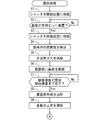
図8〜図11は、露光装置100の動作を説明するための模式図である。図8〜図11においては、筐体121内およびハウジング161内の構成の理解を容易にするために、一部の構成要素の図示が省略されるとともに、筐体121およびハウジング161の輪郭が一点鎖線で示される。図12、図13および図14は、図7の制御部110により行われる露光処理の一例を示すフローチャートである。以下、図8〜図11を参照しながら制御部110による露光処理を説明する。
(4) Exposure Processing FIGS. 8 to 11 are schematic views for explaining the operation of the
図8に示すように、露光処理の初期状態においては、シャッタ131が閉塞位置にあり、載置板151が待機位置にあり、遮光部材191が非遮光位置にある。また、筐体121内の酸素濃度は、酸素濃度計181により常時または定期的に計測され、濃度取得部5により取得されている。この時点においては、酸素濃度計181により計測される筐体121内の酸素濃度は大気中の酸素濃度に等しい。
As shown in FIG. 8, in the initial state of the exposure process, the
まず、閉塞制御部1は、図9に示すように、シャッタ131を開放位置に移動させる(ステップS1)。これにより、搬送開口121aを通して処理対象の基板Wを複数の支持ピン142の上端部に載置することができる。本例では、後述する図15の搬送装置220により基板Wが複数の支持ピン142の上端部に載置される。
First, the
次に、閉塞制御部1は、基板Wが複数の支持ピン142の上端部に載置されたか否かを判定する(ステップS2)。基板Wが載置されていない場合、閉塞制御部1は、基板Wが複数の支持ピン142の上端部に載置されるまで待機する。基板Wが載置された場合、閉塞制御部1は、シャッタ131を閉塞位置に移動させる(ステップS3)。
Next, the
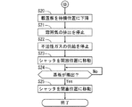
続いて、排気制御部3は、図1の吸引装置173により筐体121内の雰囲気を排出させる(ステップS4)。また、給気制御部4は、図1の配管171p,172pを通して筐体121内に不活性ガスを供給させる(ステップS5)。ステップS4,S5の処理は、いずれが先に開始されてもよいし、同時に開始されてもよい。その後、昇降制御部2は、図10に示すように、載置板151を待機位置から上昇させることにより、載置板151に基板Wを載置させる(ステップS6)。この時点で基板Wの載置面と照度計183の受光面との高さが一致する。
Subsequently, the
次に、濃度比較部6は、筐体121内の酸素濃度が露光開始濃度まで低下したか否かを判定する(ステップS7)。酸素濃度が露光開始濃度まで低下していない場合、濃度比較部6は、酸素濃度が露光開始濃度まで低下するまで待機する。酸素濃度が露光開始濃度まで低下した場合、投光制御部12は、光源部163により真空紫外線を出射させる(ステップS8)。これにより、光源部163から透光板162を通して真空紫外線が基板Wに照射され、被処理面に形成されたDSA膜の露光が開始される。また、昇降制御部2は、載置板151の上昇を開始させる(ステップS9)。
Next, the density comparison unit 6 determines whether or not the oxygen concentration in the
続いて、照度取得部8は、照度計183に真空紫外線の照度の計測を開始させ、計測された照度を照度計183から取得する(ステップS10)。さらに、遮光制御部7は、遮光部材191を遮光位置と非遮光位置との間で複数回往復移動させる(ステップS11)。ステップS8〜S11の処理は、いずれが先に開始されてもよいし、同時に開始されてもよい。
Subsequently, the illuminance acquisition unit 8 causes the
照度補間部9は、遮光期間の真空紫外線の照度を補間する(ステップS12)。露光量算出部10は、照度取得部8により取得される真空紫外線の照度および照度補間部9により補間される真空紫外線の照度を積算することにより基板Wに照射される真空紫外線の露光量を算出する(ステップS13)。
The
その後、昇降制御部2は、載置板151が処理位置に到達したか否かを判定する(ステップS14)。載置板151が処理位置に到達していない場合には、昇降制御部2はステップS16の処理に進む。一方、載置板151が処理位置に到達した場合には、昇降制御部2は、載置板151の上昇を停止させる(ステップS15)。なお、図11に示すように、載置板151が処理位置に到達した場合には、基板Wが透光板162に近接する。
After that, the elevating
次に、露光量比較部11は、露光量算出部10により算出された露光量が設定露光量に到達したか否かを判定する(ステップS16)。露光量が設定露光量に到達していない場合、露光量比較部11は、ステップS10の処理に戻る。露光量が設定露光量に到達するまで、ステップS10〜S16の処理が繰り返される。
Next, the exposure
露光量が設定露光量に到達した場合、投光制御部12は、光源部163からの真空紫外線の出射を停止させる(ステップS17)。また、照度取得部8は、照度計183による照度の計測を停止させる(ステップS18)。さらに、遮光制御部7は、遮光部材191の移動を停止させる(ステップS19)。本例では、遮光部材191は非遮光位置に戻される。
When the exposure amount reaches the set exposure amount, the light
次に、昇降制御部2は、図10に示すように、載置板151を待機位置に下降させる(ステップS20)。これにより、基板Wが載置板151から複数の支持ピン142に受け渡される。続いて、排気制御部3は、吸引装置173による筐体121内の雰囲気の排出を停止させる(ステップS21)。また、給気制御部4は、配管171p,172pからの筐体121内への不活性ガスの供給を停止させる(ステップS22)。ステップS17〜S22の処理は、いずれが先に開始されてもよいし、同時に開始されてもよい。
Next, as shown in FIG. 10, the elevating
その後、閉塞制御部1は、図9に示すように、シャッタ131を開放位置に移動させる(ステップS23)。これにより、搬送開口121aを通して露光後の基板Wを複数の支持ピン142上から筐体121の外部へ搬出することができる。本例では、後述する図15の搬送装置220により基板Wが複数の支持ピン142上から筐体121の外部へ搬出される。
After that, the
次に、閉塞制御部1は、基板Wが複数の支持ピン142上から搬出されたか否かを判定する(ステップS24)。基板Wが搬出されていない場合、閉塞制御部1は、基板Wが複数の支持ピン142上から搬出されるまで待機する。基板Wが搬出された場合、閉塞制御部1は、図8に示すように、シャッタ131を閉塞位置に移動させ(ステップS25)、露光処理を終了する。上記の動作が繰り返されることにより、複数の基板Wに露光処理を順次行うことができる。
Next, the
上記の露光処理においては、載置板151が処理位置に移動される前に光源部163から基板Wに真空紫外線が照射される。この場合、載置板151が待機位置から処理位置へ移動する過程においても基板Wに真空紫外線が照射される。そのため、基板Wの露光がより短時間で終了する。これにより、基板Wの露光処理の効率をより向上させることができる。
In the above exposure process, the substrate W is irradiated with vacuum ultraviolet rays from the
一方で、載置板151が処理位置に移動された後に光源部163から基板Wに真空紫外線が照射されてもよい。すなわち、ステップS9,S14,S15の処理がステップS6〜S8の処理の間に実行されてもよく、ステップS7の処理と同時に実行されてもよい。この場合、筐体121内の酸素濃度を露光開始濃度まで低下させる期間に載置板151を待機位置に移動させることができる。そのため、基板Wの露光がより短時間で終了する。これにより、基板Wの露光処理の効率をより向上させることができる。
On the other hand, the substrate W may be irradiated with vacuum ultraviolet rays from the
また、上記の露光処理においては、基板Wの露光量が設定露光量に到達した後に載置板151が処理位置から待機位置に移動するが、本発明はこれに限定されない。基板Wの露光量が設定露光量に到達する前に載置板151が処理位置から待機位置に移動してもよい。すなわち、ステップS20の処理がステップS16の処理の前に実行されてもよい。この場合、載置板151が処理位置から待機位置へ移動する過程においても基板Wに真空紫外線が照射される。そのため、より早い時点で基板Wが処理室120から搬出され、露光処理が終了する。これにより、基板Wの露光処理の効率をより向上させることができる。
Further, in the above exposure processing, the mounting
(5)基板処理装置
図15は、図1の露光装置100を備えた基板処理装置の全体構成を示す模式的ブロック図である。以下に説明する基板処理装置200においては、ブロック共重合体の誘導自己組織化(DSA)を利用した処理が行われる。具体的には、基板Wの被処理面上に誘導自己組織化材料を含む処理液が塗布される。その後、誘導自己組織化材料に生じるミクロ相分離により基板Wの被処理面上に2種類の重合体のパターンが形成される。2種類の重合体のうち一方のパターンが溶剤により除去される。
(5) Substrate Processing Device FIG. 15 is a schematic block diagram showing an overall configuration of a substrate processing device provided with the
誘導自己組織化材料を含む処理液をDSA液と呼ぶ。また、ミクロ相分離により基板Wの被処理面上に形成される2種類の重合体のパターンのうち一方を除去する処理を現像処理と呼び、現像処理に用いられる溶剤を現像液と呼ぶ。 The treatment liquid containing the induced self-assembling material is called a DSA liquid. Further, a process of removing one of two types of polymer patterns formed on the surface to be processed of the substrate W by microphase separation is called a developing process, and a solvent used for the developing process is called a developing solution.
図15に示すように、基板処理装置200は、露光装置100に加えて、制御装置210、搬送装置220、熱処理装置230、塗布装置240および現像装置250を備える。制御装置210は、例えばCPUおよびメモリ、またはマイクロコンピュータを含み、搬送装置220、熱処理装置230、塗布装置240および現像装置250の動作を制御する。また、制御装置210は、図1の露光装置100の閉塞部130、昇降部150、投光部160、置換部170および遮光部190の動作を制御するための指令を制御部110に与える。
As shown in FIG. 15, the
搬送装置220は、処理対象の基板Wを保持しつつその基板Wを露光装置100、熱処理装置230、塗布装置240および現像装置250の間で搬送する。熱処理装置230は、塗布装置240による塗布処理および現像装置250による現像処理の前後に基板Wの熱処理を行う。
The
塗布装置240は、基板Wの被処理面にDSA液を供給することにより、膜の塗布処理を行う。本実施の形態では、DSA液として、2種類の重合体から構成されるブロック共重合体が用いられる。2種類の重合体の組み合わせとして、例えば、ポリスチレン−ポリメチルメタクリレート(PS−PMMA)、ポリスチレン−ポリジメチルシロキサン(PS−PDMS)、ポリスチレン−ポリフェロセニルジメチルシラン(PS−PFS)、ポリスチレン−ポリエチレンオキシド(PS−PEO)、ポリスチレン−ポリビニルピリジン(PS−PVP)、ポリスチレン−ポリヒドロキシスチレン(PS−PHOST)、およびポリメチルメタクリレート−ポリメタクリレートポリヘドラルオリゴメリックシルセスキオキサン(PMMA−PMAPOSS)等が挙げられる。
The
現像装置250は、基板Wの被処理面に現像液を供給することにより、膜の現像処理を行う。現像液の溶媒として、例えば、トルエン、ヘプタン、アセトン、プロピレングリコールモノメチルエーテルアセテート(PGMEA)、プロピレングリコールモノメチルエーテル(PGME)、シクロヘキサノン、酢酸、テトラヒドロフラン、イソプロピルアルコール(IPA)または水酸化テトラメチルアンモニウム(TMAH)等が挙げられる。
The developing
図16は、図15の基板処理装置200による基板Wの処理の一例を示す模式図である。図16では、処理が行われるごとに変化する基板Wの状態が断面図で示される。本例では、基板Wが基板処理装置200に搬入される前の初期状態として、図16(a)に示すように、基板Wの被処理面を覆うように下地層L1が形成され、下地層L1上に例えばフォトレジストからなるガイドパターンL2が形成されている。以下、図15および図16を用いて基板処理装置200の動作を説明する。
FIG. 16 is a schematic view showing an example of processing of the substrate W by the
搬送装置220は、処理対象の基板Wを、熱処理装置230および塗布装置240に順に搬送する。この場合、熱処理装置230において、基板Wの温度がDSA膜L3の形成に適した温度に調整される。また、塗布装置240において、基板Wの被処理面にDSA液が供給され、塗布処理が行われる。それにより、図16(b)に示すように、ガイドパターンL2が形成されていない下地層L1上の領域に、2種類の重合体から構成されるDSA膜L3が形成される。
The
次に、搬送装置220は、DSA膜L3が形成された基板Wを、熱処理装置230および露光装置100に順に搬送する。この場合、熱処理装置230において、基板Wの加熱処理が行われることにより、DSA膜L3にミクロ相分離が生じる。これにより、図16(c)に示すように、一方の重合体からなるパターンQ1および他方の重合体からなるパターンQ2が形成される。本例では、ガイドパターンL2に沿うように、線状のパターンQ1および線状のパターンQ2が指向的に形成される。
Next, the
その後、熱処理装置230において、基板Wが冷却される。また、露光装置100において、ミクロ相分離後のDSA膜L3の全体にDSA膜L3を改質させるための真空紫外線が照射され、露光処理が行われる。これにより、一方の重合体と他方の重合体との間の結合が切断され、パターンQ1とパターンQ2とが分離される。
After that, the substrate W is cooled in the
続いて、搬送装置220は、露光装置100による露光処理後の基板Wを、熱処理装置230および現像装置250に順に搬送する。この場合、熱処理装置230において、基板Wが冷却される。また、現像装置250において、基板W上のDSA膜L3に現像液が供給され、現像処理が行われる。これにより、図16(d)に示すように、パターンQ1が除去され、最終的に、基板W上にパターンQ2が残存する。最後に、搬送装置220は、現像処理後の基板Wを現像装置250から回収する。
Subsequently, the
(6)効果
本実施の形態に係る露光装置100においては、酸素濃度計181により計測される処理室120内の酸素濃度が露光開始濃度まで低下した時点で、光源部163による基板Wへの真空紫外線の照射が開始される。ここで、露光開始濃度は、1%よりも高くかつ大気中の酸素濃度よりも低く、真空紫外線の照射により酸素原子から生成されるオゾンが基板Wの被処理面の膜に損傷を与えないように予め定められる。
(6) Effect In the
したがって、処理室120内の酸素濃度が1%まで低下する時点よりも早い時点で光源部163から基板Wに真空紫外線が照射される。また、この時点で基板Wに真空紫外線を照射することによりわずかにオゾンが発生するが、このオゾンによっては基板Wの被処理面に形成された膜には損傷が与えられない。そのため、露光処理に要する時間を短縮することができる。これにより、基板Wの露光処理の効率を向上させることができる。
Therefore, the substrate W is irradiated with the vacuum ultraviolet rays from the
[2]第2の実施の形態
第2の実施の形態に係る露光装置および基板処理装置について、第1の実施の形態に係る露光装置および基板処理装置と異なる点を説明する。図17は、本発明の第2の実施の形態における露光装置の断面斜視図である。図18は、図17の露光装置100の縦断面図である。図17および図18においては、露光装置100の内部構成の理解を容易にするため、一部の構成要素の図示を省略している。
[2] Second Embodiment The exposure apparatus and the substrate processing apparatus according to the second embodiment will be described which are different from the exposure apparatus and the substrate processing apparatus according to the first embodiment. FIG. 17 is a cross-sectional perspective view of the exposure apparatus according to the second embodiment of the present invention. FIG. 18 is a vertical sectional view of the
図18に示すように、本実施の形態に係る露光装置100においては、照度計183が固定部材124により筐体121の内側面に固定される。照度計183は、平面視において透光板162の1つの角部近傍に重なり、かつ受光素子の受光面が処理位置における基板Wの被処理面と略同一の高さに位置するように配置される。このように、本実施の形態においては、照度計183は載置板151には取り付けられないので、載置板151は照度計183を取り付けるための図2の角部151cを有さない。
As shown in FIG. 18, in the
また、図17および図18に示すように、本実施の形態に係る露光装置100は、図3の遮光部190に代えて遮光部190Aを含む。遮光部190Aは、遮光部材191、駆動装置192および棒形状の支持部材194を含む。遮光部材191は、例えばシャッタであり、光源部163から照度計183に照射される真空紫外線を遮光する遮光位置と、真空紫外線を遮光しない非遮光位置との間で移動可能に設けられる。
Further, as shown in FIGS. 17 and 18, the
駆動装置192は、例えばステッピングモータであり、回転可能な駆動軸192aを有する。駆動装置192は、駆動軸192aが上方を向くように筐体121の下面に取り付けられる。支持部材194は、上下方向に延びるように遮光部材191と駆動装置192の駆動軸192aとを連結する。駆動装置192の駆動軸192aが上下方向に平行な軸を中心に回転することにより、遮光部材191が遮光位置と非遮光位置との間で移動する。
The
本実施の形態においては、照度計183は上下方向に移動しない。そのため、露光処理においては、基板Wが処理位置に移動され、基板Wの被処理面と照度計183の受光素子の受光面とが略同一の高さになった後に、光源部163から真空紫外線が出射されることが好ましい。したがって、本実施の形態における露光処理においては、図12〜図14のステップS9,S14,S15の処理がステップS6〜S8の処理の間に実行されることが好ましい。
In this embodiment, the
[3]第3の実施の形態
第3の実施の形態に係る露光装置および基板処理装置について、第1の実施の形態に係る露光装置および基板処理装置と異なる点を説明する。図19は、本発明の第3の実施の形態における露光装置の断面斜視図である。図20は、図19の露光装置100の縦断面図である。図19および図20においては、露光装置100の内部構成の理解を容易にするため、一部の構成要素の図示を省略している。
[3] Third Embodiment The exposure apparatus and the substrate processing apparatus according to the third embodiment will be described which are different from the exposure apparatus and the substrate processing apparatus according to the first embodiment. FIG. 19 is a cross-sectional perspective view of the exposure apparatus according to the third embodiment of the present invention. FIG. 20 is a vertical sectional view of the
図19および図20に示すように、本実施の形態に係る露光装置100は、図3の遮光部190に代えて遮光部190Bを含む。遮光部190Bは、遮光部材191を含まない点を除き、図3の遮光部190と同様の構成を有する。支持部材194は、遮光部材191に代えて照度計183を一端部により支持する。第2の実施の形態と同様に、本実施の形態においては、照度計183は載置板151には取り付けられないので、載置板151は照度計183を取り付けるための図2の角部151cを有さない。
As shown in FIGS. 19 and 20, the
駆動装置192の駆動軸192aが進退することにより、図20に矢印で示すように、照度計183が真空紫外線を受光可能な非遮光位置と、真空紫外線を受光不可能な遮光位置との間で移動する。図20においては、非遮光位置における照度計183が実線で図示され、遮光位置における照度計183が一点鎖線で図示される。具体的には、非遮光位置は、平面視において、透光板162の1つの角部近傍に重なる位置である。遮光位置は、平面視において、透光板162よりも外方の位置である。
As the
すなわち、本実施の形態においては、露光処理中に、遮光部材191ではなく照度計183が非遮光位置と遮光位置との間で移動する。したがって、本実施の形態の露光処理においては、図13のステップS11で、遮光部材191ではなく照度計183が非遮光位置と遮光位置との間で移動される。また、図13のステップS19で、遮光部材191ではなく照度計183の移動が停止される。
That is, in the present embodiment, the
また、本実施の形態においても、非受光期間において基板Wに照射される真空紫外線の照度が補間されることが好ましい。本実施の形態の非受光期間における照度の補間方式は、第1の実施の形態の遮光期間における照度の補間方式と同様である。 Further, also in the present embodiment, it is preferable that the illuminance of the vacuum ultraviolet rays applied to the substrate W during the non-light receiving period is interpolated. The interpolation method of the illuminance in the non-light receiving period of the present embodiment is the same as the interpolation method of the illuminance in the light blocking period of the first embodiment.
さらに、本実施の形態においては、第2の実施の形態と同様に、照度計183は上下方向に移動しない。そのため、露光処理においては、基板Wが処理位置に移動され、基板Wの被処理面と照度計183の受光素子の受光面とが略同一の高さになった後に、光源部163から真空紫外線が出射されることが好ましい。したがって、本実施の形態における露光処理においては、図12〜図14のステップS9,S14,S15の処理がステップS6〜S8の処理の間に実行されることが好ましい。
Further, in the present embodiment, the
[4]他の実施の形態
(1)第1〜第3の実施の形態において、処理液としてDSA液が用いられるが、本発明はこれに限定されない。DSA液とは異なる他の処理液が用いられてもよい。
[4] Other Embodiments (1) In the first to third embodiments, the DSA liquid is used as the treatment liquid, but the present invention is not limited thereto. Other treatment liquids different from the DSA liquid may be used.
(2)第1〜第3の実施の形態において、真空紫外線の出射面は基板Wの被処理面よりも大きく、基板Wの全面露光が行われるが、本発明はこれに限定されない。真空紫外線の出射面は基板Wの被処理面よりも小さくてもよいし、面状の真空紫外線が出射されなくてもよい。この場合、真空紫外線の出射面と基板Wの被処理面とが相対的に移動されることにより基板Wの被処理面の全体に真空紫外線が照射される。 (2) In the first to third embodiments, the emission surface of the vacuum ultraviolet rays is larger than the surface to be treated of the substrate W, and the entire surface of the substrate W is exposed, but the present invention is not limited thereto. The emission surface of the vacuum ultraviolet rays may be smaller than the surface to be treated of the substrate W, or the planar vacuum ultraviolet rays may not be emitted. In this case, the emission surface of the vacuum ultraviolet rays and the surface to be processed of the substrate W are relatively moved, so that the entire surface to be processed of the substrate W is irradiated with the vacuum ultraviolet rays.
(3)第1〜第3の実施の形態において、露光処理時に筐体121内に不活性ガスが供給されるが、本発明はこれに限定されない。露光処理時に筐体121内の酸素濃度が十分に低減可能である場合には、筐体121内に不活性ガスが供給されなくてもよい。
(3) In the first to third embodiments, the inert gas is supplied into the
(4)第1〜第3の実施の形態において、透光板162は矩形状を有するが、本発明はこれに限定されない。透光板162は、矩形状以外の多角形状、円形状、長円形状または楕円形状等の他の形状を有してもよい。この場合、照度計183は、平面視において、透光板162と基板Wの被処理面との非重複領域に重なる位置に配置される。これにより、照度計183は基板Wと干渉することなく真空紫外線の照度を計測することができる。
(4) In the first to third embodiments, the
(5)第1の実施の形態において、照度計183が載置板151に取り付けられるが、本発明はこれに限定されない。照度計183が載置板151の移動に追従して上下方向に移動可能である限り、照度計183は載置板151に取り付けられなくてもよい。この場合において、照度計183は、載置板151と共通の駆動装置153により移動可能に構成されてもよいし、駆動装置153とは異なる駆動装置により移動可能に構成されてもよい。
(5) In the first embodiment, the
(6)第2の実施の形態において、露光装置100に遮光部190Aが設けられるが、本発明はこれに限定されない。露光装置100に遮光部190Aではなく第1の実施の形態と同様の遮光部190が設けられてもよい。
(6) In the second embodiment, the
(7)第2の実施の形態において、照度計183が固定され、遮光部材191が駆動装置192により移動可能に構成されるが、本発明はこれに限定されない。遮光部材191が固定され、照度計183が駆動装置192により移動可能に構成されてもよい。すなわち、照度計183と遮光部材191とは、相対的に移動可能であればよい。この構成においては、照度計183と遮光部材191とが平面視において重なる位置が遮光位置となり、照度計183と遮光部材191とが平面視において重ならない位置が非遮光位置となる。
(7) In the second embodiment, the
なお、第1の実施の形態においても、遮光部材191が固定され、照度計183が駆動装置192により移動可能に構成されてもよい。この場合においては、照度計183が取り付けられた載置板151の角部151cが、円形部151bとは独立して水平面内で移動可能に構成されることが好ましい。
Also in the first embodiment, the light-shielding
(8)第1〜第3の実施の形態において、照度計183は、受光面が処理位置における基板Wの被処理面と略同一の高さになるように配置されるが、本発明はこれに限定されない。照度計183は、受光面が処理位置における基板Wの被処理面を基準とする一定の高さに位置するように配置されてもよい。また、照度計183が十分な正確さで真空紫外線の照度を計測可能である場合には、第2および第3の実施の形態において、処理位置に移動される過程の基板Wに照射される真空紫外線を計測してもよい。
(8) In the first to third embodiments, the
(9)第1〜第3の実施の形態において、露光装置100が遮光部190,190A,190Bを含むが、本発明はこれに限定されない。露光装置100は遮光部190,190A,190Bを含まなくてもよい。したがって、遮光期間における照度の補間が行われなくてもよく、制御部110は、遮光制御部7および照度補間部9を含まなくてもよい。
(9) In the first to third embodiments, the
[5]請求項の各構成要素と実施の形態の各部との対応関係
以下、請求項の各構成要素と実施の形態の各構成要素との対応の例について説明するが、本発明は下記の例に限定されない。
[5] Correspondence between each component of the claim and each part of the embodiment The following describes an example of the correspondence between each component of the claim and each component of the embodiment. Not limited to the example.
上記実施の形態においては、基板Wが基板の例であり、処理室120が処理室の例であり、光源部163が光源部の例であり、吸引装置173が排気部の例であり、酸素濃度計181が酸素濃度計の例であり、照度計183が照度計の例であり、露光量算出部10が露光量算出部の例であり、投光制御部12が光源制御部の例であり、露光装置100が露光装置の例であり、配管171p,172pが給気部の例であり、載置板151が載置部の例である。昇降制御部2が載置制御部の例であり、塗布装置240が塗布処理部の例であり、熱処理装置230が熱処理部の例であり、現像装置250が現像処理部の例であり、基板処理装置200が基板処理装置の例である。
In the above embodiment, the substrate W is an example of a substrate, the
請求項の各構成要素として、請求項に記載されている構成または機能を有する他の種々の構成要素を用いることもできる。 As each component of the claim, various other components having the configuration or function described in the claim can also be used.
1…閉塞制御部,2…昇降制御部,3…排気制御部,4…給気制御部,5…濃度取得部,6…濃度比較部,7…遮光制御部,8…照度取得部,9…照度補間部,10…露光量算出部,11…露光量比較部,12…投光制御部,100…露光装置,110…制御部,120…処理室,121…筐体,121a…搬送開口,121b,141a…開口部,122…環状部材,123…被覆部材,130…閉塞部,131…シャッタ,131a,s1〜s3…シール部材,132,152,195…連結部材,133,153,192…駆動装置,133a,133b,153a,153b…位置センサ,140…受渡部,141…支持板,142…支持ピン,150…昇降部,151…載置板,151a…貫通孔,151b…円形部,151c…角部,160…投光部,161…ハウジング,162…透光板,163…光源部,164…電源装置,170…置換部,171p〜173p…配管,171v〜173v…バルブ,173…吸引装置,173a,173b…枝管,180…計測部,181…酸素濃度計,182…オゾン濃度計,183…照度計,190,190A,190B…遮光部,191…遮光部材,191a…水平板,191b…垂直板,192a…駆動軸,193…ガイド部,194…支持部材,200…基板処理装置,210…制御装置,220…搬送装置,230…熱処理装置,240…塗布装置,250…現像装置,L1…下地層,L2…ガイドパターン,L3…DSA膜,Q1,Q2…パターン,W…基板 1 ... Blockage control unit, 2 ... Elevation control unit, 3 ... Exhaust control unit, 4 ... Air supply control unit, 5 ... Concentration acquisition unit, 6 ... Concentration comparison unit, 7 ... Shading control unit, 8 ... Illuminance acquisition unit, 9 ... Illuminance interpolation unit, 10 ... Exposure calculation unit, 11 ... Exposure comparison unit, 12 ... Light projection control unit, 100 ... Exposure device, 110 ... Control unit, 120 ... Processing room, 121 ... Housing, 121a ... Conveyance opening , 121b, 141a ... opening, 122 ... annular member, 123 ... covering member, 130 ... closing part, 131 ... shutter, 131a, s1 to s3 ... sealing member, 132, 152, 195 ... connecting member, 133, 153, 192. ... Drive device, 133a, 133b, 153a, 153b ... Position sensor, 140 ... Delivery part, 141 ... Support plate, 142 ... Support pin, 150 ... Elevating part, 151 ... Mounting plate, 151a ... Through hole, 151b ... Circular part , 151c ... corner, 160 ... floodlight, 161 ... housing, 162 ... translucent plate, 163 ... light source, 164 ... power supply, 170 ... replacement, 171p to 173p ... piping, 171v to 173v ... valve, 173 ... suction device, 173a, 173b ... branch pipe, 180 ... measuring unit, 181 ... oxygen concentration meter, 182 ... ozone concentration meter, 183 ... illuminance meter, 190, 190A, 190B ... shading part, 191 ... shading member, 191a ... horizontal Plate, 191b ... Vertical plate, 192a ... Drive shaft, 193 ... Guide unit, 194 ... Support member, 200 ... Board processing device, 210 ... Control device, 220 ... Conveyor device, 230 ... Heat treatment device, 240 ... Coating device, 250 ... Developer, L1 ... Underlayer, L2 ... Guide pattern, L3 ... DSA film, Q1, Q2 ... Pattern, W ... Substrate
Claims (16)
前記処理室に収容された基板に真空紫外線を照射可能に設けられた光源部と、
前記処理室内の雰囲気を排気する排気部と、
前記処理室内の酸素濃度を計測する酸素濃度計と、
前記光源部から基板への真空紫外線の照射期間に、真空紫外線の一部を受光し、受光した真空紫外線の照度を計測する照度計と、
前記照度計により計測される照度に基づいて基板の露光量を算出する露光量算出部と、
前記酸素濃度計により計測される酸素濃度が予め定められた露光開始濃度まで低下した時点で前記光源部による基板への真空紫外線の照射を開始し、前記露光量算出部により算出される露光量が予め定められた設定露光量まで上昇した時点で前記光源部による基板への真空紫外線の照射を停止するように前記光源部を制御する光源制御部とを備え、
前記露光開始濃度は、体積比で1%よりも高くかつ大気中の酸素濃度よりも低く、真空紫外線の照射により酸素原子から生成されるオゾンが基板の被処理面の膜に損傷を与えないように予め定められる、露光装置。 A processing chamber for accommodating a substrate having a film formed on the surface to be processed, and
A light source unit provided so as to be able to irradiate a substrate housed in the processing chamber with vacuum ultraviolet rays, and a light source unit.
An exhaust unit that exhausts the atmosphere in the processing room,
An oxygen concentration meter that measures the oxygen concentration in the processing chamber,
An illuminometer that receives a part of the vacuum ultraviolet rays during the irradiation period of the vacuum ultraviolet rays from the light source unit to the substrate and measures the illuminance of the received vacuum ultraviolet rays.
An exposure amount calculation unit that calculates the exposure amount of the substrate based on the illuminance measured by the illuminance meter, and
When the oxygen concentration measured by the oxygen densitometer drops to a predetermined exposure start density, the light source unit starts irradiating the substrate with vacuum ultraviolet rays, and the exposure amount calculated by the exposure amount calculation unit is calculated. A light source control unit that controls the light source unit so as to stop the irradiation of the substrate with vacuum ultraviolet rays by the light source unit when the exposure amount rises to a predetermined set exposure amount is provided.
The exposure start density is higher than 1% by volume and lower than the oxygen concentration in the atmosphere so that ozone generated from oxygen atoms by irradiation with vacuum ultraviolet rays does not damage the film on the surface to be treated of the substrate. An exposure device that is predetermined to.
前記処理室内と外部との間での基板の受け渡しの際に前記載置部が第1の位置に移動し、前記光源部から基板への真空紫外線の照射期間前または照射期間中に前記載置部が前記第1の位置の上方の第2の位置に移動するように前記載置部を制御する載置制御部とをさらに備える、請求項1または2記載の露光装置。 A mounting section provided below the light source section and on which the substrate is mounted, and a mounting section.
When the substrate is transferred between the processing chamber and the outside, the pre-described part moves to the first position, and the pre-described part is placed before or during the irradiation period of the vacuum ultraviolet rays from the light source unit to the substrate. The exposure apparatus according to claim 1 or 2, further comprising a mounting control unit that controls the previously described mounting unit so that the unit moves to a second position above the first position.
前記塗布処理部により膜が形成された基板を熱処理する熱処理部と、
前記熱処理部により熱処理された基板を露光する請求項1〜12のいずれか一項に記載の露光装置と、
前記露光装置により露光された基板に溶剤を供給することにより基板の膜を現像する現像処理部とを備える、基板処理装置。 A coating treatment unit that forms a film on the substrate by applying the treatment liquid to the substrate,
A heat treatment unit that heat-treats the substrate on which the film is formed by the coating treatment unit, and a heat treatment unit.
The exposure apparatus according to any one of claims 1 to 12 , which exposes the substrate heat-treated by the heat-treated portion.
A substrate processing apparatus including a development processing unit that develops a film of the substrate by supplying a solvent to the substrate exposed by the exposure apparatus.
前記処理室内の雰囲気を排気部により排気するステップと、
前記処理室内の酸素濃度を酸素濃度計により計測するステップと、
前記酸素濃度計により計測される酸素濃度が予め定められた露光開始濃度まで低下した時点で、光源部による基板への真空紫外線の照射を開始するステップと、
前記光源部から基板への真空紫外線の照射期間に、照度計により真空紫外線の一部を受光し、受光した真空紫外線の照度を計測するステップと、
前記照度計により計測される照度に基づいて基板の露光量を算出するステップと、
前記算出される露光量が予め定められた設定露光量まで上昇した時点で前記光源部による基板への真空紫外線の照射を停止するステップとを含み、
前記露光開始濃度は、体積比で1%よりも高くかつ大気中の酸素濃度よりも低く、真空紫外線の照射により酸素原子から生成されるオゾンが基板の被処理面の膜に損傷を与えないように予め定められる、露光方法。 A step of accommodating a substrate having a film formed on the surface to be processed in a processing chamber,
The step of exhausting the atmosphere in the processing room by the exhaust unit,
The step of measuring the oxygen concentration in the processing chamber with an oxygen concentration meter,
When the oxygen concentration measured by the oxygen densitometer drops to a predetermined exposure start density, the step of starting the irradiation of the substrate with vacuum ultraviolet rays by the light source unit and
During the irradiation period of the vacuum ultraviolet rays from the light source unit to the substrate, a part of the vacuum ultraviolet rays is received by the illuminometer, and the illuminance of the received vacuum ultraviolet rays is measured.
The step of calculating the exposure amount of the substrate based on the illuminance measured by the illuminometer, and
The step includes a step of stopping the irradiation of the substrate with vacuum ultraviolet rays by the light source unit when the calculated exposure amount rises to a predetermined set exposure amount.
The exposure start density is higher than 1% by volume and lower than the oxygen concentration in the atmosphere so that ozone generated from oxygen atoms by irradiation with vacuum ultraviolet rays does not damage the film on the surface to be treated of the substrate. Predetermined exposure method.
前記塗布処理部により膜が形成された基板を熱処理部により熱処理するステップと、
前記熱処理部により熱処理された基板を露光装置により露光する請求項15記載の露光方法と、
前記露光装置により露光された基板の被処理面に現像処理部により溶剤を供給することにより基板の膜を現像するステップとを含む、基板処理方法。 The step of forming a film on the substrate by applying the treatment liquid to the surface to be treated of the substrate by the coating treatment unit, and
The step of heat-treating the substrate on which the film is formed by the coating treatment section by the heat treatment section,
The exposure method according to claim 15, wherein the substrate heat-treated by the heat-treated portion is exposed by an exposure apparatus.
A substrate processing method comprising a step of developing a film of a substrate by supplying a solvent to a surface to be processed of the substrate exposed by the exposure apparatus by a developing processing unit.
Priority Applications (5)
| Application Number | Priority Date | Filing Date | Title |
|---|---|---|---|
| JP2017038235A JP6985803B2 (en) | 2017-03-01 | 2017-03-01 | Exposure equipment, substrate processing equipment, substrate exposure method and substrate processing method |
| TW107103946A TWI659275B (en) | 2017-03-01 | 2018-02-05 | Exposure device, substrate processing apparatus, exposure method and substrate processing method |
| US15/902,037 US10401736B2 (en) | 2017-03-01 | 2018-02-22 | Exposure device, substrate processing apparatus, exposure method of substrate and substrate processing method |
| CN201810163638.5A CN108535966B (en) | 2017-03-01 | 2018-02-27 | Exposure apparatus, substrate processing apparatus, exposure method, and substrate processing method |
| KR1020180024538A KR102103632B1 (en) | 2017-03-01 | 2018-02-28 | Exposure device, substrate processing apparatus, exposure method of substrate and substrate processing method |
Applications Claiming Priority (1)
| Application Number | Priority Date | Filing Date | Title |
|---|---|---|---|
| JP2017038235A JP6985803B2 (en) | 2017-03-01 | 2017-03-01 | Exposure equipment, substrate processing equipment, substrate exposure method and substrate processing method |
Publications (3)
| Publication Number | Publication Date |
|---|---|
| JP2018147917A JP2018147917A (en) | 2018-09-20 |
| JP2018147917A5 JP2018147917A5 (en) | 2020-03-26 |
| JP6985803B2 true JP6985803B2 (en) | 2021-12-22 |
Family
ID=63355130
Family Applications (1)
| Application Number | Title | Priority Date | Filing Date |
|---|---|---|---|
| JP2017038235A Active JP6985803B2 (en) | 2017-03-01 | 2017-03-01 | Exposure equipment, substrate processing equipment, substrate exposure method and substrate processing method |
Country Status (5)
| Country | Link |
|---|---|
| US (1) | US10401736B2 (en) |
| JP (1) | JP6985803B2 (en) |
| KR (1) | KR102103632B1 (en) |
| CN (1) | CN108535966B (en) |
| TW (1) | TWI659275B (en) |
Families Citing this family (4)
| Publication number | Priority date | Publication date | Assignee | Title |
|---|---|---|---|---|
| WO2016133103A1 (en) * | 2015-02-18 | 2016-08-25 | 株式会社ブイ・テクノロジー | Scanning exposure device |
| TWI747490B (en) * | 2019-09-19 | 2021-11-21 | 日商斯庫林集團股份有限公司 | Exposure device |
| JP7475232B2 (en) * | 2020-07-22 | 2024-04-26 | 株式会社ディスコ | Protective member forming device |
| CN113176712A (en) * | 2021-04-25 | 2021-07-27 | 上海图双精密装备有限公司 | Exposure device suitable for contact type photoetching machine |
Family Cites Families (23)
| Publication number | Priority date | Publication date | Assignee | Title |
|---|---|---|---|---|
| JP3378271B2 (en) | 1992-06-11 | 2003-02-17 | 株式会社ニコン | Exposure method and apparatus, and device manufacturing method using the method |
| US5763892A (en) | 1995-06-19 | 1998-06-09 | Dainippon Screen Manufacturing Company, Ltd. | Ultraviolet irradiator for substrate, substrate treatment system, and method of irradiating substrate with ultraviolet light |
| TW416532U (en) | 1996-03-26 | 2000-12-21 | C Sun Mfg Ltd | Energy integrating controller of exposure machine |
| JPH10284407A (en) | 1997-04-08 | 1998-10-23 | Nikon Corp | Aligner and method for fabricating semiconductor devices using aligner |
| JP2000100685A (en) | 1998-09-17 | 2000-04-07 | Nikon Corp | Aligner and exposure method using the same |
| JP2001110710A (en) | 1999-10-08 | 2001-04-20 | Nikon Corp | Aligner, exposing method and manufacturing method of semiconductor device |
| US6211942B1 (en) * | 2000-03-10 | 2001-04-03 | Howa Machinery Ltd. | Double-sided exposure system |
| JP2001284236A (en) | 2000-03-31 | 2001-10-12 | Canon Inc | Projection exposure system and exposure method |
| JP4485282B2 (en) | 2004-08-06 | 2010-06-16 | シャープ株式会社 | Exposure apparatus, exposure amount control method, exposure amount control program and recording medium therefor |
| EP1906251A1 (en) * | 2006-09-26 | 2008-04-02 | Carl Zeiss SMT AG | Projection exposure method and projection exposure system |
| JP4952375B2 (en) * | 2007-05-23 | 2012-06-13 | 株式会社明電舎 | Resist removing method and apparatus |
| US20110130009A1 (en) * | 2009-11-30 | 2011-06-02 | Lam Research Ag | Method and apparatus for surface treatment using a mixture of acid and oxidizing gas |
| CN203037348U (en) | 2012-12-04 | 2013-07-03 | 彩虹(佛山)平板显示有限公司 | Detection device for detecting quantity of collected light on surface of glass substrate |
| JP6099970B2 (en) * | 2012-12-27 | 2017-03-22 | キヤノン株式会社 | Exposure apparatus and device manufacturing method |
| JP6099969B2 (en) * | 2012-12-27 | 2017-03-22 | キヤノン株式会社 | Exposure apparatus and device manufacturing method |
| DE102013204466A1 (en) * | 2013-03-14 | 2014-09-18 | Carl Zeiss Smt Gmbh | Measurement of an optical symmetry property on a projection exposure apparatus |
| US9318663B2 (en) * | 2013-07-10 | 2016-04-19 | Epistar Corporation | Light-emitting element |
| JP6535197B2 (en) | 2014-04-28 | 2019-06-26 | 株式会社ブイ・テクノロジー | Exposure apparatus and exposure method |
| KR101681636B1 (en) * | 2014-11-28 | 2016-12-02 | 세메스 주식회사 | Apparatus and method for edge exposure, Apparatus for treating a substrate |
| JP6543064B2 (en) | 2015-03-25 | 2019-07-10 | 株式会社Screenホールディングス | Exposure apparatus, substrate processing apparatus, substrate exposure method and substrate processing method |
| JP6495707B2 (en) * | 2015-03-25 | 2019-04-03 | 株式会社Screenホールディングス | Exposure apparatus and substrate processing apparatus |
| JP2017044537A (en) * | 2015-08-25 | 2017-03-02 | ウシオ電機株式会社 | Illuminometer, light irradiation device and illuminance measurement method |
| JP6872385B2 (en) * | 2017-03-01 | 2021-05-19 | 株式会社Screenホールディングス | Exposure equipment, substrate processing equipment, substrate exposure method and substrate processing method |
-
2017
- 2017-03-01 JP JP2017038235A patent/JP6985803B2/en active Active
-
2018
- 2018-02-05 TW TW107103946A patent/TWI659275B/en active
- 2018-02-22 US US15/902,037 patent/US10401736B2/en active Active
- 2018-02-27 CN CN201810163638.5A patent/CN108535966B/en active Active
- 2018-02-28 KR KR1020180024538A patent/KR102103632B1/en active IP Right Grant
Also Published As
| Publication number | Publication date |
|---|---|
| US10401736B2 (en) | 2019-09-03 |
| JP2018147917A (en) | 2018-09-20 |
| CN108535966A (en) | 2018-09-14 |
| CN108535966B (en) | 2021-07-02 |
| KR20180100495A (en) | 2018-09-11 |
| TW201833686A (en) | 2018-09-16 |
| KR102103632B1 (en) | 2020-04-22 |
| TWI659275B (en) | 2019-05-11 |
| US20180253012A1 (en) | 2018-09-06 |
Similar Documents
| Publication | Publication Date | Title |
|---|---|---|
| JP6543064B2 (en) | Exposure apparatus, substrate processing apparatus, substrate exposure method and substrate processing method | |
| JP6985803B2 (en) | Exposure equipment, substrate processing equipment, substrate exposure method and substrate processing method | |
| US10955745B2 (en) | Exposure device, substrate processing apparatus, exposure method and substrate processing method | |
| JP6495707B2 (en) | Exposure apparatus and substrate processing apparatus | |
| JP6811119B2 (en) | Exposure equipment, substrate processing equipment, substrate exposure method and substrate processing method | |
| JP6768561B2 (en) | Exposure equipment, substrate processing equipment, substrate exposure method and substrate processing method | |
| JP6845058B2 (en) | Exposure equipment, substrate processing equipment, substrate exposure method and substrate processing method | |
| JP6924661B2 (en) | Exposure equipment, substrate processing equipment, exposure method and substrate processing method | |
| JP6894281B2 (en) | Exposure equipment, substrate processing equipment, substrate exposure method and substrate processing method | |
| TWI682433B (en) | Exposure device, substrate processing apparatus, exposure method for substrate and substrate processing method | |
| JP7002262B2 (en) | Exposure equipment, substrate processing equipment, exposure method and substrate processing method |
Legal Events
| Date | Code | Title | Description |
|---|---|---|---|
| A621 | Written request for application examination |
Free format text: JAPANESE INTERMEDIATE CODE: A621 Effective date: 20191223 |
|
| A521 | Request for written amendment filed |
Free format text: JAPANESE INTERMEDIATE CODE: A523 Effective date: 20200214 |
|
| A131 | Notification of reasons for refusal |
Free format text: JAPANESE INTERMEDIATE CODE: A131 Effective date: 20201117 |
|
| A521 | Request for written amendment filed |
Free format text: JAPANESE INTERMEDIATE CODE: A523 Effective date: 20210112 |
|
| A131 | Notification of reasons for refusal |
Free format text: JAPANESE INTERMEDIATE CODE: A131 Effective date: 20210421 |
|
| A521 | Request for written amendment filed |
Free format text: JAPANESE INTERMEDIATE CODE: A523 Effective date: 20210604 |
|
| TRDD | Decision of grant or rejection written | ||
| A01 | Written decision to grant a patent or to grant a registration (utility model) |
Free format text: JAPANESE INTERMEDIATE CODE: A01 Effective date: 20211102 |
|
| A61 | First payment of annual fees (during grant procedure) |
Free format text: JAPANESE INTERMEDIATE CODE: A61 Effective date: 20211126 |
|
| R150 | Certificate of patent or registration of utility model |
Ref document number: 6985803 Country of ref document: JP Free format text: JAPANESE INTERMEDIATE CODE: R150 |