JP6971538B2 - Communication equipment, communication methods, programs, and communication systems - Google Patents
Communication equipment, communication methods, programs, and communication systems Download PDFInfo
- Publication number
- JP6971538B2 JP6971538B2 JP2016099930A JP2016099930A JP6971538B2 JP 6971538 B2 JP6971538 B2 JP 6971538B2 JP 2016099930 A JP2016099930 A JP 2016099930A JP 2016099930 A JP2016099930 A JP 2016099930A JP 6971538 B2 JP6971538 B2 JP 6971538B2
- Authority
- JP
- Japan
- Prior art keywords
- data
- parity
- bit
- error
- transmission
- Prior art date
- Legal status (The legal status is an assumption and is not a legal conclusion. Google has not performed a legal analysis and makes no representation as to the accuracy of the status listed.)
- Active
Links
- 230000006854 communication Effects 0.000 title claims description 121
- 238000004891 communication Methods 0.000 title claims description 119
- 238000000034 method Methods 0.000 title claims description 32
- 230000005540 biological transmission Effects 0.000 claims description 90
- 238000001514 detection method Methods 0.000 claims description 73
- 238000012790 confirmation Methods 0.000 claims description 20
- 238000012546 transfer Methods 0.000 claims description 12
- 238000012545 processing Methods 0.000 claims description 8
- 101000741965 Homo sapiens Inactive tyrosine-protein kinase PRAG1 Proteins 0.000 description 13
- 102100038659 Inactive tyrosine-protein kinase PRAG1 Human genes 0.000 description 13
- 238000010586 diagram Methods 0.000 description 4
- 238000005516 engineering process Methods 0.000 description 4
- 125000004122 cyclic group Chemical group 0.000 description 2
- 230000006870 function Effects 0.000 description 1
- 238000012986 modification Methods 0.000 description 1
- 230000004048 modification Effects 0.000 description 1
- 230000002265 prevention Effects 0.000 description 1
- 230000004044 response Effects 0.000 description 1
Images


Classifications
-
- H—ELECTRICITY
- H04—ELECTRIC COMMUNICATION TECHNIQUE
- H04L—TRANSMISSION OF DIGITAL INFORMATION, e.g. TELEGRAPHIC COMMUNICATION
- H04L1/00—Arrangements for detecting or preventing errors in the information received
- H04L1/004—Arrangements for detecting or preventing errors in the information received by using forward error control
- H04L1/0056—Systems characterized by the type of code used
- H04L1/0061—Error detection codes
-
- G—PHYSICS
- G06—COMPUTING; CALCULATING OR COUNTING
- G06F—ELECTRIC DIGITAL DATA PROCESSING
- G06F11/00—Error detection; Error correction; Monitoring
- G06F11/07—Responding to the occurrence of a fault, e.g. fault tolerance
- G06F11/08—Error detection or correction by redundancy in data representation, e.g. by using checking codes
- G06F11/10—Adding special bits or symbols to the coded information, e.g. parity check, casting out 9's or 11's
- G06F11/1008—Adding special bits or symbols to the coded information, e.g. parity check, casting out 9's or 11's in individual solid state devices
- G06F11/1012—Adding special bits or symbols to the coded information, e.g. parity check, casting out 9's or 11's in individual solid state devices using codes or arrangements adapted for a specific type of error
- G06F11/1032—Simple parity
-
- H—ELECTRICITY
- H04—ELECTRIC COMMUNICATION TECHNIQUE
- H04L—TRANSMISSION OF DIGITAL INFORMATION, e.g. TELEGRAPHIC COMMUNICATION
- H04L1/00—Arrangements for detecting or preventing errors in the information received
- H04L1/08—Arrangements for detecting or preventing errors in the information received by repeating transmission, e.g. Verdan system
Landscapes
- Engineering & Computer Science (AREA)
- Theoretical Computer Science (AREA)
- Signal Processing (AREA)
- Computer Networks & Wireless Communication (AREA)
- General Engineering & Computer Science (AREA)
- General Physics & Mathematics (AREA)
- Physics & Mathematics (AREA)
- Quality & Reliability (AREA)
- Information Transfer Systems (AREA)
- Detection And Prevention Of Errors In Transmission (AREA)
- Detection And Correction Of Errors (AREA)
- Bus Control (AREA)
- Error Detection And Correction (AREA)
- Stereo-Broadcasting Methods (AREA)
- Reduction Or Emphasis Of Bandwidth Of Signals (AREA)
Description
本開示は、通信装置、通信方法、プログラム、および、通信システムに関し、特に、より確実に通信を行うことができるようにした通信装置、通信方法、プログラム、および、通信システムに関する。 The present disclosure relates to communication devices, communication methods, programs, and communication systems, and more particularly to communication devices, communication methods, programs, and communication systems that enable more reliable communication.
従来、複数のデバイスが実装されたボード内でバスを介したデバイス間の通信に用いられるバスIF(Interface)として、例えば、I2C(Inter-Integrated Circuit)が多く利用されている。 Conventionally, for example, I2C (Inter-Integrated Circuit) is often used as a bus IF (Interface) used for communication between devices via a bus in a board on which a plurality of devices are mounted.
また、近年、I2Cの高速化を実現することが求められており、次世代の規格としてI3C(Improved Inter Integrated Circuit)の規定が進行している。I3Cでは、マスタおよびスレーブは、2本の信号線を用いて双方向に通信を行うことができ、例えば、マスタからスレーブへのデータ転送(ライト転送)と、スレーブからマスタへのデータ転送(リード転送)とが行われる。 In recent years, it has been required to realize high-speed I2C, and the regulation of I3C (Improved Inter Integrated Circuit) is in progress as a next-generation standard. In I3C, the master and slave can communicate in both directions using two signal lines, for example, data transfer from master to slave (write transfer) and data transfer from slave to master (read). Transfer) and is performed.
例えば、特許文献1には、ホスト・プロセッサとサブシステム・コントローラとを、I2Cにより相互接続するディジタル・データ処理システムが開示されている。また、特許文献2には、標準I2Cプロトコルの上部に層状に配置された通信プロトコルを実現する方法が開示されている。
For example,
ところで、上述したようなI3Cでは、例えば、マスタおよびスレーブにおいて、パリティやCRC(Cyclic Redundancy Check)などによるエラー検出が行われることが規定されているが、そのようなエラー検出が用意されていない信号の送受信も行われる。そのため、エラー検出が用意されていない信号にエラーが発生したときに、マスタおよびスレーブのどちらもデータ信号線に対する駆動を行わない状態となることがあった。そのため、例えば、受信したデータが正しいものであるかを検出することが困難になり、正常な通信を行うことができなくなることが懸念される。 By the way, in I3C as described above, for example, it is stipulated that error detection by parity or CRC (Cyclic Redundancy Check) is performed in master and slave, but such error detection is not prepared. Is also sent and received. Therefore, when an error occurs in a signal for which error detection is not prepared, neither the master nor the slave may be in a state of driving the data signal line. Therefore, for example, it becomes difficult to detect whether the received data is correct, and there is a concern that normal communication cannot be performed.
本開示は、このような状況に鑑みてなされたものであり、より確実に通信を行うことができるようにするものである。 This disclosure has been made in view of such a situation, and is intended to enable more reliable communication.
本開示の第1の側面の通信装置は、他の通信装置と信号の送受信を行うことによって、リードコマンドの送信に続くプリアンブルの送受信の後にデータを受信する送受信部と、前記送受信部が受信したデータに対するパリティチェックを行うことでエラーの発生を検出するエラー検出部とを備え、前記プリアンブルの2ビット目は、前記他の通信装置によって駆動され、前記リードコマンドの受信の成功または失敗を示す信号であり、前記エラー検出部は、前記データに含まれている2ビットのパリティのうち、一方を偶数パリティとし、他方を奇数パリティとしてエラー検出を行うことで、前記データが全て1または0である場合であっても、そのデータが正しいものであるのか、前記プリアンブルの2ビット目に1ビットエラーが発生したことによってデータ信号線に対する駆動が行われない状態によるものであるのかを判断する。 The communication device according to the first aspect of the present disclosure includes a transmission / reception unit that receives data after transmission / reception of a preamble following transmission of a read command by transmitting / receiving signals to / from another communication device, and a transmission / reception unit that receives the data. It is equipped with an error detection unit that detects the occurrence of an error by performing a parity check on the data, and the second bit of the preamble is driven by the other communication device and is a signal indicating success or failure of reception of the read command. The error detection unit performs error detection with one of the 2-bit parity contained in the data as an even parity and the other as an odd parity, so that the data are all 1 or 0. Even in this case, it is determined whether the data is correct or whether it is due to a state in which the data signal line is not driven due to the occurrence of a 1-bit error in the second bit of the preamble.
本開示の第1の側面の通信方法またはプログラムは、他の通信装置と信号の送受信を行うことによって、リードコマンドの送信に続くプリアンブルの送受信の後にデータを受信し、受信したデータに対するパリティチェックを行うことでエラーの発生を検出し、前記プリアンブルの2ビット目は、前記他の通信装置によって駆動され、前記リードコマンドの受信の成功または失敗を示す信号であり、前記データに含まれている2ビットのパリティのうち、一方を偶数パリティとし、他方を奇数パリティとしてエラー検出を行うことで、前記データが全て1または0である場合であっても、そのデータが正しいものであるのか、前記プリアンブルの2ビット目に1ビットエラーが発生したことによってデータ信号線に対する駆動が行われない状態によるものであるのかを判断する。
The communication method or program of the first aspect of the present disclosure receives data after transmission / reception of a preamble following transmission of a read command by transmitting / receiving signals with another communication device, and performs a parity check for the received data. By doing so, the occurrence of an error is detected, and the second bit of the preamble is a signal driven by the other communication device and indicating success or failure of reception of the read command, and is included in the
本開示の第1の側面においては、他の通信装置と信号の送受信が行われることによって、リードコマンドの送信に続くプリアンブルの送受信の後にデータが受信され、受信したデータに対するパリティチェックを行うことでエラーの発生が検出される。そして、プリアンブルの2ビット目は、他の通信装置によって駆動され、リードコマンドの受信の成功または失敗を示す信号であり、データに含まれている2ビットのパリティのうち、一方が偶数パリティとされ、他方が奇数パリティとされてエラー検出が行われることで、データが全て1または0である場合であっても、そのデータが正しいものであるのか、プリアンブルの2ビット目に1ビットエラーが発生したことによってデータ信号線に対する駆動が行われない状態によるものであるのかが判断される。 In the first aspect of the present disclosure, data is received after transmission / reception of a preamble following transmission of a read command by transmitting / receiving a signal with another communication device, and a parity check is performed on the received data. The occurrence of an error is detected. The second bit of the preamble is a signal that is driven by another communication device and indicates success or failure of reception of the read command, and one of the two-bit parity contained in the data is an even parity. , The other is an odd parity and error detection is performed, so even if the data is all 1 or 0, a 1-bit error occurs in the 2nd bit of the preamble, whether the data is correct. By doing so, it is determined whether the data signal line is not driven.
本開示の第2の側面の通信システムは、バスにおける制御の主導権を有する第1の通信装置と、前記第1の通信装置による制御に従って通信を行う第2の通信装置とを備え、前記第1の通信装置が、信号の送受信を行うことによって、リードコマンドの送信に続くプリアンブルの送受信の後にデータを受信する送受信部と、前記送受信部が受信したデータに対するパリティチェックを行うことでエラーの発生を検出するエラー検出部とを有し、前記プリアンブルの2ビット目は、前記他の通信装置によって駆動され、前記リードコマンドの受信の成功または失敗を示す信号であり、前記エラー検出部は、前記データに含まれている2ビットのパリティのうち、一方を偶数パリティとし、他方を奇数パリティとしてエラー検出を行うことで、前記データが全て1または0である場合であっても、そのデータが正しいものであるのか、前記プリアンブルの2ビット目に1ビットエラーが発生したことによってデータ信号線に対する駆動が行われない状態によるものであるのかを判断する。 The communication system of the second aspect of the present disclosure includes a first communication device having the initiative of control in the bus and a second communication device that communicates according to the control by the first communication device. 1 communication equipment is, by transmitting and receiving signals, an error by performing a transceiver for receiving data after the transmission and reception of a preamble followed by the transmission of a read command, a parity check for the data to which the transmission and reception unit receives The preamble has an error detection unit for detecting the occurrence, and the second bit of the preamble is a signal driven by the other communication device to indicate success or failure of reception of the read command, and the error detection unit is Of the 2-bit parity contained in the data, one is set to even parity and the other is set to odd parity to perform error detection, so that even if the data is all 1 or 0, the data can be obtained. It is determined whether the data is correct or the data signal line is not driven due to the occurrence of a 1-bit error in the second bit of the preamble.
本開示の第2の側面においては、信号の送受信が行われることによって、リードコマンドの送信に続くプリアンブルの送受信の後にデータが受信され、受信したデータに対するパリティチェックを行うことでエラーの発生が検出される。そして、プリアンブルの2ビット目は、他の通信装置によって駆動され、リードコマンドの受信の成功または失敗を示す信号であり、データに含まれている2ビットのパリティのうち、一方が偶数パリティとされ、他方が奇数パリティとされてエラー検出が行われることで、データが全て1または0である場合であっても、そのデータが正しいものであるのか、プリアンブルの2ビット目に1ビットエラーが発生したことによってデータ信号線に対する駆動が行われない状態によるものであるのかが判断される。 In the second aspect of the present disclosure, by transmitting and receiving signals, data is received after transmission and reception of a preamble following transmission of a read command, and error occurrence is detected by performing a parity check on the received data. Will be done. The second bit of the preamble is a signal that is driven by another communication device and indicates success or failure of reception of the read command, and one of the two-bit parity contained in the data is an even parity. , The other is an odd parity and error detection is performed, so even if the data is all 1 or 0, a 1-bit error occurs in the 2nd bit of the preamble, whether the data is correct. By doing so, it is determined whether the data signal line is not driven.
本開示の第1および第2の側面によれば、より確実に通信を行うことができる。 According to the first and second aspects of the present disclosure, communication can be performed more reliably.
以下、本技術を適用した具体的な実施の形態について、図面を参照しながら詳細に説明する。 Hereinafter, specific embodiments to which the present technology is applied will be described in detail with reference to the drawings.
<バスIFの構成例> <Bus IF configuration example>
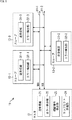
図1は、本技術を適用したバスIFの一実施の形態の構成例を示すブロック図である。 FIG. 1 is a block diagram showing a configuration example of an embodiment of a bus IF to which the present technology is applied.
図1に示されているバスIF11は、マスタ12と3台のスレーブ13−1乃至13−3とが、データ信号線14−1およびクロック信号線14−2を介して接続されて構成される。
The bus IF 11 shown in FIG. 1 is configured by connecting a
マスタ12は、バスIF11における制御の主導権を有しており、データ信号線14−1およびクロック信号線14−2を介して、スレーブ13−1乃至13−3と通信を行うことができる。
The
スレーブ13−1乃至13−3は、マスタ12による制御に従って、データ信号線14−1およびクロック信号線14−2を介して、マスタ12と通信を行うことができる。なお、スレーブ13−1乃至13−3は、それぞれ同様に構成されており、以下、それらを区別する必要がない場合、単にスレーブ13と称し、スレーブ13を構成する各ブロックについても同様とする。
The slaves 13-1 to 13-3 can communicate with the
データ信号線14−1およびクロック信号線14−2は、マスタ12およびスレーブ13の間で信号を伝送するのに用いられる。例えば、バスIF11では、データ信号線14−1を介して、1ビットずつ逐次的にシリアルデータ(SDA:Serial Data)が伝送され、クロック信号線14−2を介して、所定の周波数のシリアルクロック(SCL:Serial Clock)が伝送される。
The data signal line 14-1 and the clock signal line 14-2 are used to transmit signals between the
また、バスIF11では、I3Cの規格に準じて、通信速度が異なる複数の伝送方式が規定されており、マスタ12は、それらの伝送方式を切り替えることができる。例えば、バスIF11では、データの転送レートに応じて、通常の転送レートでデータ通信を行うSDR(Standard Data Rate)モード、および、SDRモードよりも高い転送レートでデータ通信を行うHDR(High Data Rate)モードが規定されている。また、HDRモードでは、DDR(Double Data Rate)モード、TSP(Ternary Symbol Pure-Bus)モード、および、TSL(Ternary Symbol Legacy-inclusive-Bus)モードの3つのモードが規格で定義されている。なお、バスIF11では、通信を開始するときにはSDRモードで通信を行うことが規定されている。
Further, the bus IF 11 defines a plurality of transmission methods having different communication speeds according to the I3C standard, and the
マスタ12は、送受信部21、エラー検出部22、確認信号検出部23、およびコンフリクト回避部24を備えて構成される。
The
送受信部21は、データ信号線14−1およびクロック信号線14−2を介して、スレーブ13と信号の送受信を行う。例えば、送受信部21は、クロック信号線14−2を駆動することにより送信するシリアルクロックのタイミングに合わせて、データ信号線14−1に対する駆動を行う(電位をHレベルまたはLレベルに切り替える)ことにより、スレーブ13に信号を送信する。また、送受信部21は、クロック信号線14−2のシリアルクロックのタイミングに合わせて、スレーブ13がデータ信号線14−1に対する駆動を行うことによって、スレーブ13から送信されてくる信号を受信する。なお、クロック信号線14−2に対する駆動は、常に、マスタ12側により行われる。さらに、送受信部21は、スレーブ13に送信するデータに、後述するようなパリティを付加して送信を行う。
The transmission /
エラー検出部22は、送受信部21が受信した信号に発生しているエラーを検出する。例えば、エラー検出部22は、送受信部21が受信した信号に対するパリティチェックや巡回冗長検査(CRC)などを行ったり、スレーブ13からマスタ12へ送信権を移行する際に発行されるトークンを確認したりすることで、エラーを検出することができる。そして、エラー検出部22は、送受信部21が受信した信号にエラーが発生していることを検出した場合、例えば、送受信部21に対してスレーブ13との通信を最初からやり直すように指示することができる。
The error detection unit 22 detects an error occurring in the signal received by the transmission /
確認信号検出部23は、送受信部21から送信された信号を受信したスレーブ13から送信されてくるACK(受信確認信号)またはNACK(非受信確認信号)を検出することにより、スレーブ13がコマンドやデータなどの受信に成功したか否かを確認する。例えば、バスIF11では、信号にエラーが発生せずに、スレーブ13がコマンドやデータなどの受信に成功したときには、スレーブ13からマスタ12にACKを送信するように規定されている。また、バスIF11では、信号にエラーが発生して、スレーブ13がコマンドやデータなどの受信に失敗したときには、スレーブ13からマスタ12にNACKを送信するように規定されている。
The confirmation
従って、確認信号検出部23は、マスタ12から送信されるコマンドやデータなどに対して、スレーブ13から送信されてくるACKを検出した場合には、スレーブ13がコマンドやデータなどを受信することに成功したと確認することができる。一方、確認信号検出部23は、マスタ12から送信されるコマンドやデータなどに対して、スレーブ13から送信されてくるNACKを検出した場合には、スレーブ13がコマンドやデータなどを受信することに失敗したと確認することができる。
Therefore, when the confirmation
コンフリクト回避部24は、例えば、確認信号検出部23によりNACKが検出された場合、NACKに続く所定数のビットを無視した後に、通信を途中で遮断することを指示するアボート信号を送信するように、送受信部21に対する指示を行う。これにより、コンフリクト回避部24は、例えば、スレーブ13から送信されるリードデータと、マスタ12から送信されるHDR終了コマンドによりコンフリクトが発生することを回避することができる。なお、マスターアボートを確実に行うために、リードデータの後に送受信されるプリアンブルの2ビット目に対する駆動は、マスタ12が常に行う。
For example, when NACK is detected by the confirmation
さらに、コンフリクト回避部24は、送受信部21により、CRCワードの送信を指示するプリアンブルが受信され、エラー検出部22により、そのプリアンブルに続いて受信された信号にトークンエラーまたはCRCエラーの発生が検出された場合、プリアンブルに続いて、CRCワードとリードデータとの差に対応するビット数に応じたクロックを送信した後に、通信を途中で遮断することを指示するアボート信号を送信するように、送受信部21に対する指示を行う。これにより、コンフリクト回避部24は、例えば、スレーブ13から送信されるリードデータと、マスタ12から送信されるHDR終了コマンドによりコンフリクトが発生することを回避することができる。
Further, the
スレーブ13は、送受信部31およびエラー検出部32を備えて構成される。
The
送受信部31は、データ信号線14−1およびクロック信号線14−2を介して、マスタ12と信号の送受信を行う。例えば、送受信部31は、クロック信号線14−2のシリアルクロックのタイミングに合わせて、マスタ12がデータ信号線14−1に対する駆動を行うことによって、マスタ12から送信されてくる信号を受信する。また、送受信部31は、クロック信号線14−2のシリアルクロックのタイミングに合わせて、データ信号線14−1に対する駆動を行うことによって、マスタ12に信号を送信する。さらに、送受信部31は、マスタ12に送信するデータに、後述するようなパリティを付加して送信を行う。
The transmission / reception unit 31 transmits / receives a signal to / from the
エラー検出部32は、マスタ12のエラー検出部22と同様に、送受信部31が受信した信号に発生しているエラーを検出する。そして、エラー検出部32は、送受信部31が受信した信号にエラーが発生していない場合、その信号により伝送されるコマンドやデータなどの受信に成功したことを伝えるACKを、送受信部31によりマスタ12に送信させる。一方、エラー検出部32は、送受信部31が受信した信号にエラーが発生していた場合、その信号により伝送されるコマンドやデータなどの受信に失敗したことを伝えるNACKを、送受信部31によりマスタ12に送信させる。
The error detection unit 32 detects an error occurring in the signal received by the transmission / reception unit 31, similarly to the error detection unit 22 of the
さらに、エラー検出部32は、例えば、送受信部31が受信した信号にエラーが発生し、正常な通信を行うことができない場合には、その後の一切の通信を無視し、マスタ12に対する応答を停止してスレーブ13を待機状態とさせる。
Further, for example, when an error occurs in the signal received by the transmission / reception unit 31 and normal communication cannot be performed, the error detection unit 32 ignores all subsequent communication and stops the response to the
以上のようにバスIF11は構成されており、マスタ12およびスレーブ13は、データ信号線14−1およびクロック信号線14−2を介して信号を送受信することができる。
As described above, the bus IF 11 is configured, and the
ところで、バスIF11では、DDRモード時において、プリアンブルと呼ばれる2ビットの信号を使用して、次に送信するデータのタイプを指定するように規定されている。しかしながら、プリアンブルには、パリティやCRCによるエラー検出が用意されていないため、プリアンブルにエラーが発生した場合には、そのエラーを検出することができない。 By the way, the bus IF 11 is specified to specify the type of data to be transmitted next by using a 2-bit signal called a preamble in the DDR mode. However, since the preamble does not provide error detection by parity or CRC, if an error occurs in the preamble, the error cannot be detected.
例えば、マスタ12がスレーブ13にリードコマンドを送信したとき、リードコマンドに続いて送信されるプリアンブルでは、1ビット目はマスタ12により駆動され、2ビット目はスレーブ13により駆動される。例えば、マスタ12は、その1ビット目により、リードコマンドに続いてデータが送信されることを指定し、スレーブ13は、その2ビット目により、リードコマンドの受信に成功したか否かを送信することができる。例えば、スレーブ13は、リードコマンドに続くプリアンブルの2ビット目を0に駆動することによってリードコマンドの受信に成功したことを示すACKを送信し、その2ビット目を1に駆動することによってリードコマンドの受信に失敗したことを示すNACKを送信する。
For example, when the
しかしながら、このプリアンブルの2ビット目において、1ビットの値が反転する1ビットエラーが発生した場合、マスタ12は、エラーの発生を検出することができない。従って、スレーブ13が、リードコマンドの受信に失敗したことを伝えるNACKを送信したとき、そのNACKに1ビットエラーが発生すると、マスタ12は、スレーブ13からACKが送信されてきたと誤認識することになる。この場合、マスタ12は、スレーブ13からリードデータが送信されてくるのを待機する状態となるが、スレーブ13は、リードコマンドの受信に失敗しているため、リードデータの送信は行われない。
However, if a 1-bit error in which the value of 1 bit is inverted occurs in the second bit of this preamble, the
そのため、図2に示すように、リードコマンドに続くプリアンブルの2ビット目に1ビットエラーが発生すると、マスタ12およびスレーブ13のどちらもデータ信号線14−1に対する駆動を行わない状態となる。
Therefore, as shown in FIG. 2, when a 1-bit error occurs in the second bit of the preamble following the read command, neither the
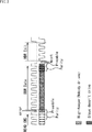
ここで、上述したように、マスタ12のエラー検出部22は、スレーブ13から送信されてくるリードデータに含まれるパリティビットを用いて、そのリードデータに発生するエラーを検出することができる。例えば、図3Aに示すように、エラー検出部22は、データの奇数ビットから求められるバリティビットP1と、データの偶数ビットから求められるバリティビットP0に基づいて、データにエラーが発生しているか否かを検出することができる。例えば、従来、バリティビットP1は、データの奇数ビットの論理和が偶数のとき0を取り、バリティビットP0は、データの偶数ビットの論理和が偶数のとき0を取るように設定されている。
Here, as described above, the error detection unit 22 of the
従って、図3Bに示すように、リードデータが全て0である場合、パリティビットP1およびP0はどちらも0となる。このため、データ信号線14−1に対するHレベル維持が行われない状態(即ち、データ信号線14−1がLレベル)で、マスタ12およびスレーブ13のいずれもデータ信号線14−1に対する駆動を行わない場合、リードデータは全て0となる。従って、この場合、実際に全て0のデータが送信されてきたときと区別することができない。
Therefore, as shown in FIG. 3B, when the read data are all 0, the parity bits P1 and P0 are both 0. Therefore, in a state where the H level is not maintained for the data signal line 14-1 (that is, the data signal line 14-1 is the L level), both the
同様に、図3Cに示すように、リードデータが全て1である場合、パリティビットP1およびP0はどちらも1となる。このため、データ信号線14−1に対するHレベル維持が行われる状態で、マスタ12およびスレーブ13のいずれもデータ信号線14−1に対する駆動を行わない場合、リードデータは全て1となる。従って、この場合、実際に全て1のデータが送信されてきたときと区別することができない。
Similarly, as shown in FIG. 3C, when the read data are all 1, the parity bits P1 and P0 are both 1. Therefore, if neither the
そこで、マスタ12のエラー検出部22は、バリティビットP1は、データの奇数ビットの論理和が偶数のとき0を取る偶数パリティとし、バリティビットP0は、データの偶数ビットの論理和が奇数のとき0を取る奇数パリティとするように設定される。なお、以下では、マスタ12のエラー検出部22の構成について説明するが、スレーブ13のエラー検出部32も同様に構成されている。そして、送受信部21および送受信部31により、以下で説明するようなパリティが付加されてデータが送信される。
Therefore, the error detection unit 22 of the
これにより、例えば、図4Aに示すように、リードデータが全て0である場合、バリティビットP1は0となり、バリティビットP0は1となる。同様に、例えば、図4Bに示すように、リードデータが全て1である場合、バリティビットP1は0となり、バリティビットP0は1となる。このため、エラー検出部22は、マスタ12およびスレーブ13のいずれもデータ信号線14−1に対する駆動を行わない場合、パリティが一致しないことより、受信したデータは正確ではなく、エラーが発生していることを検出することができる。
As a result, for example, as shown in FIG. 4A, when the read data are all 0, the variety bit P1 becomes 0 and the variety bit P0 becomes 1. Similarly, for example, as shown in FIG. 4B, when the read data are all 1, the variety bit P1 becomes 0 and the variety bit P0 becomes 1. Therefore, when neither the
<パリティエラー検出器の第1の構成例> <First configuration example of the parity error detector>
マスタ12のエラー検出部22は、図5に示すようなパリティエラー検出器41を有して構成される。
The error detection unit 22 of the
図5に示すように、パリティエラー検出器41は、入力端子42、XORゲート43および44、1ビット付加部45、並びに、出力端子46および47を備えて構成される。
As shown in FIG. 5, the
パリティエラー検出器41の入力端子42には、データ信号線14−1を介して供給されるシリアルデータが入力される。そして、シリアルデータの奇数ビットは、XORゲート43に供給され、シリアルデータの偶数ビットは、XORゲート44に供給されるように、入力端子42がXORゲート43および44に接続される。
Serial data supplied via the data signal line 14-1 is input to the
そして、パリティエラー検出器41では、XORゲート44に対して1ビット付加部45から1の値の1ビットが付加される。これにより、パリティエラー検出器41は、出力端子46から出力されるバリティビットP1は、データの奇数ビットの論理和が偶数のとき0を取り、出力端子47から出力されるバリティビットP0は、データの奇数ビットの論理和が奇数のとき0を取るように構成される。
Then, in the
このように構成されるパリティエラー検出器41は、例えば、データ信号線14−1に対するHレベル維持が行われない状態(即ち、データ信号線14−1がLレベル)で、マスタ12およびスレーブ13のいずれもデータ信号線14−1に対する駆動を行わない場合、データを正しく受信することができなかったと検出することができる。即ち、この場合、受信する信号は全て0となるが、バリティビットP1は0となり、かつ、バリティビットP0は1となるため、パリティが一致しないことよりエラーを検出すること(図4Aを参照)ができる。
The
同様に、パリティエラー検出器41は、例えば、データ信号線14−1に対するHレベル維持が行われる状態で、マスタ12およびスレーブ13のいずれもデータ信号線14−1に対する駆動を行わない場合、データを正しく受信することができなかったと検出することができる。即ち、この場合、受信する信号は全て1となるが、バリティビットP1は0となり、かつ、バリティビットP0は1となるため、パリティが一致しないことよりエラーを検出すること(図4Bを参照)ができる。
Similarly, when the
また、パリティエラー検出器41では、バリティビットP1を偶数パリティとし、バリティビットP0を奇数パリティとすることで、例えば、マスタ12がデータ信号線14−1をHレベルに維持し続ける場合を考慮すると、早期にエラーを検出することができる。即ち、マスタ12がデータ信号線14−1をHレベルに維持し続ける場合にはデータが全て1となり、バリティビットP1が0となることよりエラーを早く検出することができる。
Further, in the
<パリティチェックを正常に行う通信方法> <Communication method for normal parity check>
図6は、マスタ12が、HDRモードのひとつであるDDRモードでスレーブ13からデータを読み出す通信処理(DDR Read)を説明するフローチャートである。
FIG. 6 is a flowchart illustrating a communication process (DDR Read) in which the
ステップS11において、マスタ12は、通信をSDRモードからHDRモードに切り替える処理を行う。具体的には、マスタ12では、送受信部21が、データ信号線14−1およびクロック信号線14−2を駆動して、SDRモードにおいて、バスIF11を構成する全てのスレーブ13を対象として一斉にコマンドを送信することを通知するブロードキャストコマンド(0x7E+R/W=0)を送信する。その後、マスタ12では、ブロードキャストコマンドの受信が成功したことを確認するためにスレーブ13から送信されてくるACKを受信すると、送受信部21が、HDRモードに入るためのコモンコマンドコード(ENTHDR CCC(0x20))を送信する。
In step S11, the
ステップS12において、マスタ12の送受信部21は、データ信号線14−1およびクロック信号線14−2を駆動して、リードコマンドを送信する。
In step S12, the transmission /
ステップS13において、送受信部21は、リードコマンドを送信した後のプリアンブルの2ビット目の値を検出し、スレーブ13からACKおよびNACKのどちらが送信されてきかを判定する。即ち、送受信部21は、リードコマンドを送信した後のプリアンブルの2ビット目が0であることを検出した場合、スレーブ13からACKが送信されてきたと判定する。一方、送受信部21は、リードコマンドを送信した後のプリアンブルの2ビット目が1であることを検出した場合、スレーブ13からNACKが送信されてきたと判定する。
In step S13, the transmission /
ステップS13において、送受信部21が、スレーブ13からACKが送信されてきたと判定した場合、処理はステップS14に進む。
If the transmission /
ステップS14において、送受信部21は、スレーブ13から送信されてくるリードデータを受信する。
In step S14, the transmission /
ステップS15において、エラー検出部22は、ステップS14で送受信部21が受信したデータに対するパリティチェックを行って、データにエラーが発生しているか否かを判定する。このとき、図4を参照して上述したように、バリティビットP1は、データの奇数番目のビットの論理和が偶数のとき0を取り、バリティビットP1は、データの偶数番目のビットの論理和が奇数のとき0を取る。
In step S15, the error detection unit 22 performs a parity check on the data received by the transmission /
ステップS15において、エラー検出部22が、データにエラーが発生していない、即ち、データが正常であると判定した場合、処理はステップS16に進み、送受信部21は、データに続いて送信されてくるプリアンブルを受信する。
If the error detection unit 22 determines in step S15 that no error has occurred in the data, that is, the data is normal, the process proceeds to step S16, and the transmission /
ステップS17において、送受信部21は、ステップS16で受信したプリアンブルにより次に送信されることが指定されているのは、データおよびCRCワードのどちらであるかを判定する。
In step S17, the transmission /
ステップS17において、送受信部21が、次に送信されてくるのはデータであると判定した場合、処理はステップS18に進み、送受信部21はリードデータを受信した後、処理はステップS15に戻って、以下、同様の処理が繰り返される。
If the transmission /
一方、ステップS17において、送受信部21が、次に送信されてくるのはCRCワードであると判定した場合、処理はステップS19に進み、送受信部21はCRCワードを受信する。
On the other hand, if the transmission /
ステップS19の処理後、処理はステップS22に進む。または、ステップS15でパリティチェックの結果がエラーであると判定された場合、処理はステップS20に進み、スレーブ13に対して、処理を中断することを指示するアボート信号を送信した後、処理はステップS22に進む。また、ステップS13でNACKが送信されてきたと判定された場合、処理はステップS21に進み、所定のビット数のコンフリクト防止クロック期間の経過後、送受信部21は、スレーブ13に対して、処理を中断することを指示するアボート信号を送信して、処理はステップS22に進む。
After the processing of step S19, the processing proceeds to step S22. Alternatively, if it is determined in step S15 that the result of the parity check is an error, the process proceeds to step S20, and after transmitting an abort signal instructing the
ステップS22において、送受信部21はHDR終了コマンドを送信し、これにより、マスタ12がDDRモードでスレーブ13からデータを読み出す通信処理(DDR Read)は終了される。
In step S22, the transmission /
以上のように、バスIF11では、例えば、マスタ12がACKを受信したと判定したとき、そのACKがNACKの1ビットエラーであってデータ信号線14−1に対する駆動が行われない状態が発生したとしても、エラー検出部22がパリティチェックを行うことで、受信したデータが正しいものではないことを検出することができる。これにより、マスタ12は、受信したデータが正しいものであるのか、データ信号線14−1に対する駆動が行われない状態によるものであるのかを正確に判断して、より確実に通信を行うことができる。
As described above, in the bus IF11, for example, when it is determined that the
<パリティエラー検出器の第2の構成例> <Second configuration example of the parity error detector>
図7および図8を参照して、パリティエラー検出器41の第2の構成例について説明する。
A second configuration example of the
上述の図4および図5を参照して説明したパリティエラー検出器41は、バリティビットP1は、データの奇数ビットの論理和が偶数のとき0を取り、バリティビットP0は、データの偶数ビットの論理和が奇数のとき0を取るように構成されている。
In the
これに対し、図7および図8に示すように、パリティエラー検出器41Aは、図5のパリティエラー検出器41とは逆に、バリティビットP1は、データの奇数ビットの論理和が偶数のとき1を取り、バリティビットP0は、データの偶数ビットの論理和が奇数のとき1を取るように構成されている。
On the other hand, as shown in FIGS. 7 and 8, in the
このように構成されるパリティエラー検出器41Aにおいても、例えば、データ信号線14−1に対するHレベル維持が行われない状態(即ち、データ信号線14−1がLレベル)で、マスタ12およびスレーブ13のいずれもデータ信号線14−1に対する駆動を行わない場合、データを正しく受信することができなかったと検出することができる。即ち、この場合、図7Aに示すように、リードデータは全て0となるが、バリティビットP1は1となり、かつ、バリティビットP0は0となるため、パリティが一致しないことよりエラーを検出することができる。
Even in the
同様に、パリティエラー検出器41Aは、例えば、データ信号線14−1に対するHレベル維持が行われる状態で、マスタ12およびスレーブ13のいずれもデータ信号線14−1に対する駆動を行わない場合、データを正しく受信することができなかったと検出することができる。即ち、この場合、図7Bに示すように、リードデータは全て1となるが、バリティビットP1は1となり、かつ、バリティビットP0は0となるため、パリティが一致しないことよりエラーを検出することができる。
Similarly, when the
なお、本技術は、I3Cの規格に従ったバスIF11に限定されることはなく、その他の規格に従ったバスIF11に適用することができる。また、図1に示すバスIF11では、スレーブ13−1乃至13−3が接続された構成例が示されているが、スレーブ13は、例えば、1台または2台でもよく、あるいは、3台以上でもよい。
The present technology is not limited to the bus IF11 according to the I3C standard, and can be applied to the bus IF11 according to other standards. Further, in the bus IF 11 shown in FIG. 1, a configuration example in which slaves 13-1 to 13-3 are connected is shown, but the number of
なお、上述のフローチャートを参照して説明した各処理は、必ずしもフローチャートとして記載された順序に沿って時系列に処理する必要はなく、並列的あるいは個別に実行される処理(例えば、並列処理あるいはオブジェクトによる処理)も含むものである。また、プログラムは、1のCPUにより処理されるものであっても良いし、複数のCPUによって分散処理されるものであっても良い。 It should be noted that each process described with reference to the above flowchart does not necessarily have to be processed in chronological order in the order described as the flowchart, and is a process executed in parallel or individually (for example, a parallel process or an object). Processing by) is also included. Further, the program may be processed by one CPU or may be distributed processed by a plurality of CPUs.
また、本明細書において、システムとは、複数の装置により構成される装置全体を表すものである。 Further, in the present specification, the system represents an entire device composed of a plurality of devices.
また、上述した一連の処理は、ハードウエアにより実行することもできるし、ソフトウエアにより実行することもできる。一連の処理をソフトウエアにより実行する場合には、そのソフトウエアを構成するプログラムが、専用のハードウエアに組み込まれているコンピュータ、または、各種のプログラムをインストールすることで、各種の機能を実行することが可能な、例えば汎用のパーソナルコンピュータなどに、プログラムが記録されたプログラム記録媒体からインストールされる。 Further, the series of processes described above can be executed by hardware or by software. When a series of processes are executed by software, the programs that make up the software execute various functions by installing a computer embedded in the dedicated hardware or various programs. It can be installed, for example, on a general-purpose personal computer, from the program recording medium on which the program is recorded.
<ハードウエアの構成例> <Hardware configuration example>
図9は、上述した一連の処理をプログラムにより実行するコンピュータのハードウエアの構成例を示すブロック図である。 FIG. 9 is a block diagram showing an example of hardware configuration of a computer that executes the above-mentioned series of processes programmatically.
コンピュータにおいて、CPU(Central Processing Unit)101,ROM(Read Only Memory)102,RAM(Random Access Memory)103、およびEEPROM(Electronically Erasable and Programmable Read Only Memory)104は、バス105により相互に接続されている。バス105には、さらに、入出力インタフェース106が接続されており、入出力インタフェース106が外部(例えば、図1のデータ信号線14−1およびクロック信号線14−2)に接続される。
In a computer, a CPU (Central Processing Unit) 101, a ROM (Read Only Memory) 102, a RAM (Random Access Memory) 103, and an EEPROM (Electronically Erasable and Programmable Read Only Memory) 104 are connected to each other by a bus 105. .. An input /
以上のように構成されるコンピュータでは、CPU101が、例えば、ROM102およびEEPROM104に記憶されているプログラムを、バス105を介してRAM103にロードして実行することにより、上述した一連の処理が行われる。また、コンピュータ(CPU101)が実行するプログラムは、ROM102に予め書き込んでおく他、入出力インタフェース106を介して外部からEEPROM104にインストールしたり、更新したりすることができる。
In the computer configured as described above, the
なお、本技術は以下のような構成も取ることができる。
(1)
他の通信装置と信号の送受信を行う送受信部と、
前記送受信部が受信したデータに対するパリティチェックを行うことでエラーの発生を検出するエラー検出部と
を備え、
前記エラー検出部は、前記データに含まれている2ビットのパリティのうち、一方を偶数パリティとし、他方を奇数パリティとしてエラー検出を行う
を備える通信装置。
(2)
前記エラー検出部は、前記送受信部が受信したデータのうちの、奇数番目のビットから求められるパリティを偶数パリティとし、偶数番目のビットから求められるパリティを奇数バリティとする
上記(1)に記載の通信装置。
(3)
前記エラー検出部は、前記送受信部が受信したデータのうちの、奇数番目のビットから求められるパリティを奇数パリティとし、偶数番目のビットから求められるパリティを偶数バリティとする
上記(1)に記載の通信装置。
(4)
前記送受信部は、前記他の通信装置に送信するデータに付加する2ビットのパリティのうち、一方を偶数パリティとし、他方を奇数パリティとする
上記(1)から(3)までのいずれかに記載の通信装置。
(5)
前記通信装置は、バスにおける制御の主導権を有する通信装置であり、前記他の通信装置は、前記通信装置による制御に従って通信を行う
上記(1)から(4)までのいずれかに記載の通信装置。
(6)
前記通信装置は、バスにおける制御の主導権を有する他の通信装置による制御に従って通信を行う
上記(1)から(5)までのいずれかに記載の通信装置。
(7)
前記送受信部により、次に送信するデータのタイプを指定するプリアンブルが受信されて、そのプリアンブルに続いて受信された信号のビット列と、前記プリアンブルにより送信されることが指定されたタイプにおいて送信されるべきビット列とを比較することにより、エラーの発生を検出するエラー検出部と、
前記エラー検出部によりエラーの発生が検出された場合、前記プリアンブルに続いて所定ビット数に応じたクロックを送信した後に、通信を途中で遮断することを指示するアボート信号を送信するように、前記送受信部に対する指示を行うコンフリクト回避部と
をさらに備える上記(1)から(6)までのいずれかに記載の通信装置。
(8)
前記送受信部から送信された信号を受信した前記他の通信装置から送信されてくる受信確認信号および非受信確認信号のいずれかを検出する確認信号検出部と、
前記確認信号検出部により前記非受信確認信号が検出されたとき、前記非受信確認信号に続く所定数のビットを無視した後に、通信を途中で遮断することを指示するアボート信号を送信するように、前記送受信部に対する指示を行うコンフリクト回避部と
をさらに備える上記(1)から(7)までのいずれかに記載の通信装置。
(9)
前記送受信部は、前記他の通信装置から読み出されるリードデータを受信し、前記リードデータの後に送受信されるプリアンブルの2ビット目に対する駆動を常に行う
上記(1)から(8)までのいずれかに記載の通信装置。
(10)
前記送受信部は、通常の転送レートでデータ通信を行うSDR(Standard Data Rate)モード、および、SDRモードよりも高い転送レートでデータ通信を行うHDR(High Data Rate)モードで、信号の送受信を行うことができる
上記(1)から(9)までのいずれかに記載の通信装置。
(11)
前記送受信部は、1ビットずつ逐次的にシリアルデータを伝送するデータ信号線、および、所定の周波数のシリアルクロックを伝送するクロック信号線の2本の信号線を介して通信を行う
上記(1)から(10)までのいずれかに記載の通信装置。
(12)
前記送受信部、I3C(Improved Inter Integrated Circuit)の規格に準じた通信を行う
上記(1)から(11)までのいずれかに記載の通信装置。
(13)
他の通信装置と信号の送受信を行い、
前記送受信部が受信したデータに対するパリティチェックを行うことでエラーの発生を検出し、
前記データに含まれている2ビットのパリティのうち、一方を偶数パリティとし、他方を奇数パリティとしてエラー検出を行う
ステップを含む通信方法。
(14)
他の通信装置と信号の送受信を行い、
前記送受信部が受信したデータに対するパリティチェックを行うことでエラーの発生を検出し、
前記データに含まれている2ビットのパリティのうち、一方を偶数パリティとし、他方を奇数パリティとしてエラー検出を行う
ステップを含む通信処理をコンピュータに実行させるプログラム。
(15)
バスにおける制御の主導権を有する第1の通信装置と、
前記第1の通信装置による制御に従って通信を行う第2の通信装置と
を備え、
前記第1の通信装置および前記第2の通信装置それぞれが、
他の通信装置と信号の送受信を行う送受信部と、
前記送受信部が受信したデータに対するパリティチェックを行うことでエラーの発生を検出するエラー検出部と
を有し、
前記エラー検出部は、前記データに含まれている2ビットのパリティのうち、一方を偶数パリティとし、他方を奇数パリティとしてエラー検出を行う
通信システム。
The present technology can also have the following configurations.
(1)
A transmitter / receiver that sends / receives signals to / from other communication devices,
It is equipped with an error detection unit that detects the occurrence of an error by performing a parity check on the data received by the transmission / reception unit.
The error detection unit is a communication device including one of the 2-bit parity contained in the data, one of which is an even parity and the other of which is an odd parity for error detection.
(2)
The error detection unit has the parity obtained from the odd-numbered bits of the data received by the transmission / reception unit as the even parity, and the parity obtained from the even-numbered bits as the odd variance. Communication device.
(3)
The error detection unit has the parity obtained from the odd-numbered bits of the data received by the transmission / reception unit as the odd parity, and the parity obtained from the even-numbered bits as the even variance. Communication device.
(4)
The transmission / reception unit is described in any one of (1) to (3) above, wherein one of the two-bit parity added to the data transmitted to the other communication device is an even parity and the other is an odd parity. Communication device.
(5)
The communication device according to any one of (1) to (4) above, wherein the communication device is a communication device having an initiative of control in a bus, and the other communication device communicates according to control by the communication device. Device.
(6)
The communication device according to any one of (1) to (5) above, wherein the communication device communicates according to control by another communication device having the initiative of control in the bus.
(7)
The transmitter / receiver receives a preamble that specifies the type of data to be transmitted next, and is transmitted in the bit string of the signal received following the preamble and the type specified to be transmitted by the preamble. An error detector that detects the occurrence of an error by comparing it with a power string,
When the error detection unit detects the occurrence of an error, the preamble is followed by a clock corresponding to a predetermined number of bits, and then an abort signal instructing the communication to be cut off is transmitted. The communication device according to any one of (1) to (6) above, further comprising a conflict avoidance unit that gives an instruction to a transmission / reception unit.
(8)
A confirmation signal detection unit that detects either a reception confirmation signal or a non-reception confirmation signal transmitted from the other communication device that has received the signal transmitted from the transmission / reception unit.
When the non-reception confirmation signal is detected by the confirmation signal detection unit, after ignoring a predetermined number of bits following the non-reception confirmation signal, an abort signal instructing to cut off communication in the middle is transmitted. The communication device according to any one of (1) to (7) above, further comprising a conflict avoidance unit that gives an instruction to the transmission / reception unit.
(9)
The transmission / reception unit receives read data read from the other communication device and always drives the second bit of the preamble transmitted / received after the read data to any of the above (1) to (8). The communication device described.
(10)
The transmission / reception unit transmits / receives signals in an SDR (Standard Data Rate) mode in which data communication is performed at a normal transfer rate and an HDR (High Data Rate) mode in which data communication is performed at a transfer rate higher than that in the SDR mode. The communication device according to any one of (1) to (9) above.
(11)
The transmission / reception unit communicates via two signal lines, a data signal line that sequentially transmits serial data bit by bit and a clock signal line that transmits a serial clock of a predetermined frequency (1). The communication device according to any one of (10) to (10).
(12)
The communication device according to any one of (1) to (11) above, which performs communication according to the standard of the transmitter / receiver and I3C (Improved Inter Integrated Circuit).
(13)
Send and receive signals with other communication devices
The occurrence of an error is detected by performing a parity check on the data received by the transmission / reception unit.
A communication method including a step of performing error detection with one of the 2-bit parity included in the data as an even parity and the other as an odd parity.
(14)
Send and receive signals with other communication devices
The occurrence of an error is detected by performing a parity check on the data received by the transmission / reception unit.
A program that causes a computer to perform communication processing including a step of performing error detection with one of the two-bit parity contained in the data as an even parity and the other as an odd parity.
(15)
The first communication device that has the initiative in control on the bus,
A second communication device that communicates according to the control of the first communication device is provided.
Each of the first communication device and the second communication device
A transmitter / receiver that sends / receives signals to / from other communication devices,
The transmission / reception unit has an error detection unit that detects the occurrence of an error by performing a parity check on the received data.
The error detection unit is a communication system that detects an error by using one of the two-bit parity contained in the data as an even parity and the other as an odd parity.
なお、本実施の形態は、上述した実施の形態に限定されるものではなく、本開示の要旨を逸脱しない範囲において種々の変更が可能である。 The present embodiment is not limited to the above-described embodiment, and various modifications can be made without departing from the gist of the present disclosure.
11 バスIF, 12 マスタ, 13 スレーブ, 14−1 データ信号線, 14−2 クロック信号線, 21 送受信部, 22 エラー検出部, 23 確認信号検出部, 24 コンフリクト回避部, 31 送受信部, 32 エラー検出部, 41 パリティエラー検出器, 42 入力端子, 43および44 XORゲート, 45 1ビット付加部, 46および47 出力端子 11 Bus IF, 12 Master, 13 Slave, 14-1 Data signal line, 14-2 Clock signal line, 21 Transmission / reception unit, 22 Error detection unit, 23 Confirmation signal detection unit, 24 Conflict avoidance unit, 31 Transmission / reception unit, 32 Error Detector, 41 parity error detector, 42 input terminal, 43 and 44 XOR gate, 45 1-bit addition unit, 46 and 47 output terminal
Claims (17)
前記送受信部が受信したデータに対するパリティチェックを行うことでエラーの発生を検出するエラー検出部と
を備え、
前記プリアンブルの2ビット目は、前記他の通信装置によって駆動され、前記リードコマンドの受信の成功または失敗を示す信号であり、
前記エラー検出部は、前記データに含まれている2ビットのパリティのうち、一方を偶数パリティとし、他方を奇数パリティとしてエラー検出を行うことで、前記データが全て1または0である場合であっても、そのデータが正しいものであるのか、前記プリアンブルの2ビット目に1ビットエラーが発生したことによってデータ信号線に対する駆動が行われない状態によるものであるのかを判断する
通信装置。 A transmitter / receiver that receives data after transmission / reception of a preamble following transmission of a read command by transmitting / receiving signals to / from other communication devices.
It is equipped with an error detection unit that detects the occurrence of an error by performing a parity check on the data received by the transmission / reception unit.
The second bit of the preamble is a signal driven by the other communication device and indicating success or failure of reception of the read command.
The error detection unit performs error detection with one of the two-bit parity contained in the data as an even parity and the other as an odd parity, so that the data are all 1 or 0. However, a communication device that determines whether the data is correct or is due to a state in which the data signal line is not driven due to the occurrence of a 1-bit error in the second bit of the preamble.
請求項1に記載の通信装置。 The communication according to claim 1, wherein the error detecting unit has an even-numbered parity as the parity obtained from the odd-numbered bits of the data received by the transmitting / receiving unit, and an odd-numbered parity as the parity obtained from the even-numbered bits. Device.
請求項1に記載の通信装置。 The communication according to claim 1, wherein the error detection unit has an odd parity as the parity obtained from the odd-numbered bits of the data received by the transmission / reception unit, and an even parity as the parity obtained from the even-numbered bits. Device.
請求項1に記載の通信装置。 The communication device according to claim 1, wherein the communication device is a communication device having a control initiative in a bus, and the other communication device communicates according to control by the communication device.
前記エラー検出部によりエラーの発生が検出された場合、前記プリアンブルに続いて所定ビット数に応じたクロックを送信するように、前記送受信部に対する指示を行うコンフリクト回避部と
をさらに備える請求項1に記載の通信装置。 By comparing the bit string of the signal that the preamble is received and subsequently received by the transmitter / receiver with the bit string that should be transmitted in the type specified to be transmitted by the preamble. An error detector that detects the occurrence of an error, and an error detector
Claim 1 further includes a conflict avoidance unit that instructs the transmission / reception unit to transmit a clock according to a predetermined number of bits following the preamble when an error occurrence is detected by the error detection unit. The communication device described.
前記確認信号検出部により前記非受信確認信号が検出されたとき、前記非受信確認信号に続く所定数のビットを無視するコンフリクト回避部と
をさらに備える請求項1に記載の通信装置。 A confirmation signal detection unit that detects either a reception confirmation signal or a non-reception confirmation signal transmitted from the other communication device that has received the signal transmitted from the transmission / reception unit.
The communication device according to claim 1, further comprising a conflict avoidance unit that ignores a predetermined number of bits following the non-reception confirmation signal when the non-reception confirmation signal is detected by the confirmation signal detection unit.
請求項1に記載の通信装置。 The communication device according to claim 1, wherein the transmission / reception unit receives read data read from the other communication device and always drives the second bit of the preamble transmitted / received after the read data.
請求項1に記載の通信装置。 The transmission / reception unit transmits / receives signals in an SDR (Standard Data Rate) mode in which data communication is performed at a normal transfer rate and an HDR (High Data Rate) mode in which data communication is performed at a transfer rate higher than that in the SDR mode. The communication device according to claim 1.
請求項8に記載の通信装置。 The error detection unit checks the parity for the data received by the transmission / reception unit in the HDR mode.
The communication device according to claim 8.
請求項1に記載の通信装置。 According to claim 1, the transmission / reception unit communicates via two signal lines, a data signal line that sequentially transmits serial data bit by bit and a clock signal line that transmits a serial clock of a predetermined frequency. The communication device described.
請求項1に記載の通信装置。 The communication device according to claim 1, wherein the transmission / reception unit communicates according to the standard of I3C (Improved Inter Integrated Circuit).
受信したデータに対するパリティチェックを行うことでエラーの発生を検出し、
前記プリアンブルの2ビット目は、前記他の通信装置によって駆動され、前記リードコマンドの受信の成功または失敗を示す信号であり、
前記データに含まれている2ビットのパリティのうち、一方を偶数パリティとし、他方を奇数パリティとしてエラー検出を行うことで、前記データが全て1または0である場合であっても、そのデータが正しいものであるのか、前記プリアンブルの2ビット目に1ビットエラーが発生したことによってデータ信号線に対する駆動が行われない状態によるものであるのかを判断する
ステップを含む通信方法。 By sending and receiving signals to and from other communication devices, data is received after sending and receiving preambles following the sending of read commands.
By performing a parity check on the received data, the occurrence of an error is detected and
The second bit of the preamble is a signal driven by the other communication device and indicating success or failure of reception of the read command.
By performing error detection with one of the two-bit parity contained in the data as an even parity and the other as an odd parity, even if the data is all 1 or 0, the data can be obtained. A communication method including a step of determining whether the data signal line is correct or the data signal line is not driven due to the occurrence of a 1-bit error in the second bit of the preamble.
受信したデータに対するパリティチェックを行うことでエラーの発生を検出し、
前記プリアンブルの2ビット目は、前記他の通信装置によって駆動され、前記リードコマンドの受信の成功または失敗を示す信号であり、
前記データに含まれている2ビットのパリティのうち、一方を偶数パリティとし、他方を奇数パリティとしてエラー検出を行うことで、前記データが全て1または0である場合であっても、そのデータが正しいものであるのか、前記プリアンブルの2ビット目に1ビットエラーが発生したことによってデータ信号線に対する駆動が行われない状態によるものであるのかを判断する
ステップを含む通信処理をコンピュータに実行させるプログラム。 By sending and receiving signals to and from other communication devices, data is received after sending and receiving preambles following the sending of read commands.
By performing a parity check on the received data, the occurrence of an error is detected and
The second bit of the preamble is a signal driven by the other communication device and indicating success or failure of reception of the read command.
By performing error detection with one of the two-bit parity contained in the data as an even parity and the other as an odd parity, even if the data is all 1 or 0, the data can be obtained. A program that causes a computer to perform communication processing including a step of determining whether it is correct or whether it is due to a state in which the data signal line is not driven due to the occurrence of a 1-bit error in the second bit of the preamble. ..
前記第1の通信装置による制御に従って通信を行う第2の通信装置と
を備え、
前記第1の通信装置が、
他の通信装置と信号の送受信を行うことによって、リードコマンドの送信に続くプリアンブルの送受信の後にデータを受信する送受信部と、
前記送受信部が受信したデータに対するパリティチェックを行うことでエラーの発生を検出するエラー検出部と
を有し、
前記プリアンブルの2ビット目は、前記他の通信装置によって駆動され、前記リードコマンドの受信の成功または失敗を示す信号であり、
前記エラー検出部は、前記データに含まれている2ビットのパリティのうち、一方を偶数パリティとし、他方を奇数パリティとしてエラー検出を行うことで、前記データが全て1または0である場合であっても、そのデータが正しいものであるのか、前記プリアンブルの2ビット目に1ビットエラーが発生したことによってデータ信号線に対する駆動が行われない状態によるものであるのかを判断する
通信システム。 The first communication device that has the initiative in control on the bus,
A second communication device that communicates according to the control of the first communication device is provided.
It said first communication equipment is,
A transmitter / receiver that receives data after transmission / reception of a preamble following transmission of a read command by transmitting / receiving signals to / from other communication devices.
The transmission / reception unit has an error detection unit that detects the occurrence of an error by performing a parity check on the received data.
The second bit of the preamble is a signal driven by the other communication device and indicating success or failure of reception of the read command.
The error detection unit performs error detection with one of the two-bit parity contained in the data as an even parity and the other as an odd parity, so that the data are all 1 or 0. However, a communication system that determines whether the data is correct or whether it is due to a state in which the data signal line is not driven due to the occurrence of a 1-bit error in the second bit of the preamble.
請求項14に記載の通信システム。 The error detection unit uses the parity obtained from the odd-numbered bits of the data received by the transmission / reception unit as the even-numbered parity, and the parity obtained from the even-numbered bits as the odd-numbered parity.
The communication system according to claim 14.
請求項14に記載の通信システム。 The error detection unit sets the parity obtained from the odd-numbered bits of the data received by the transmission / reception unit to the odd-numbered parity, and sets the parity obtained from the even-numbered bits to the even-numbered parity.
The communication system according to claim 14.
前記エラー検出部によりエラーの発生が検出された場合、前記プリアンブルに続いて所定ビット数に応じたクロックを送信するように、前記送受信部に対する指示を行うコンフリクト回避部と
をさらに備える請求項14に記載の通信システム。 By comparing the bit string of the signal that the preamble is received and subsequently received by the transmitter / receiver with the bit string that should be transmitted in the type specified to be transmitted by the preamble. An error detector that detects the occurrence of an error, and an error detector
14. Claim 14 further includes a conflict avoidance unit that instructs the transmission / reception unit to transmit a clock according to a predetermined number of bits following the preamble when an error occurrence is detected by the error detection unit. The communication system described.
Priority Applications (7)
| Application Number | Priority Date | Filing Date | Title |
|---|---|---|---|
| JP2016099930A JP6971538B2 (en) | 2016-05-18 | 2016-05-18 | Communication equipment, communication methods, programs, and communication systems |
| EP17729204.2A EP3458962B1 (en) | 2016-05-18 | 2017-05-02 | Communication device and communication system |
| SG11201808956YA SG11201808956YA (en) | 2016-05-18 | 2017-05-02 | Communication device and communication system |
| CN201780029045.3A CN109074294B (en) | 2016-05-18 | 2017-05-02 | Communication device and communication system |
| US16/099,306 US10721022B2 (en) | 2016-05-18 | 2017-05-02 | Communication apparatus, communication method, program, and communication system |
| PCT/JP2017/017224 WO2017199763A1 (en) | 2016-05-18 | 2017-05-02 | Communication device and communication system |
| TW106114886A TWI771299B (en) | 2016-05-18 | 2017-05-05 | Communication apparatus, communication method, program, and communication system |
Applications Claiming Priority (1)
| Application Number | Priority Date | Filing Date | Title |
|---|---|---|---|
| JP2016099930A JP6971538B2 (en) | 2016-05-18 | 2016-05-18 | Communication equipment, communication methods, programs, and communication systems |
Publications (3)
| Publication Number | Publication Date |
|---|---|
| JP2017208710A JP2017208710A (en) | 2017-11-24 |
| JP2017208710A5 JP2017208710A5 (en) | 2019-06-27 |
| JP6971538B2 true JP6971538B2 (en) | 2021-11-24 |
Family
ID=59034818
Family Applications (1)
| Application Number | Title | Priority Date | Filing Date |
|---|---|---|---|
| JP2016099930A Active JP6971538B2 (en) | 2016-05-18 | 2016-05-18 | Communication equipment, communication methods, programs, and communication systems |
Country Status (7)
| Country | Link |
|---|---|
| US (1) | US10721022B2 (en) |
| EP (1) | EP3458962B1 (en) |
| JP (1) | JP6971538B2 (en) |
| CN (1) | CN109074294B (en) |
| SG (1) | SG11201808956YA (en) |
| TW (1) | TWI771299B (en) |
| WO (1) | WO2017199763A1 (en) |
Families Citing this family (5)
| Publication number | Priority date | Publication date | Assignee | Title |
|---|---|---|---|---|
| JP6828271B2 (en) * | 2016-05-18 | 2021-02-10 | ソニー株式会社 | Communication devices, communication methods, programs, and communication systems |
| JP6786871B2 (en) | 2016-05-18 | 2020-11-18 | ソニー株式会社 | Communication devices, communication methods, programs, and communication systems |
| CN109144913A (en) * | 2018-09-29 | 2019-01-04 | 联想(北京)有限公司 | A kind of data processing method, system and electronic equipment |
| US20200220571A1 (en) * | 2019-01-04 | 2020-07-09 | Qorvo Us, Inc. | Apparatus supporting multi-radio coexistence |
| CN116243148B (en) * | 2023-02-22 | 2024-03-15 | 成都电科星拓科技有限公司 | Debugging and verifying framework for chip I3C protocol |
Family Cites Families (32)
| Publication number | Priority date | Publication date | Assignee | Title |
|---|---|---|---|---|
| US4621323A (en) * | 1983-03-28 | 1986-11-04 | Digital Equipment Corporation | Message transmission circuitry |
| JPS63131738A (en) * | 1986-11-21 | 1988-06-03 | Hitachi Seiko Ltd | Parity check system |
| JPH06161793A (en) * | 1992-11-18 | 1994-06-10 | Fujitsu Ltd | Coping device in parity error occurrence |
| US5465262A (en) * | 1994-01-28 | 1995-11-07 | International Business Machines Corporation | Method and structure for providing error correction code and automatic parity sensing |
| US5453999A (en) * | 1994-04-26 | 1995-09-26 | Unisys Corporation | Address verification system using parity for transmitting and receiving circuits |
| US5566193A (en) * | 1994-12-30 | 1996-10-15 | Lucent Technologies Inc. | Method and apparatus for detecting and preventing the communication of bit errors on a high performance serial data link |
| US5835511A (en) * | 1996-05-17 | 1998-11-10 | Advanced Micro Devices, Inc. | Method and mechanism for checking integrity of byte enable signals |
| JPH10334044A (en) * | 1997-06-03 | 1998-12-18 | Oki Electric Ind Co Ltd | Serial interface method |
| US6356984B1 (en) | 1998-06-30 | 2002-03-12 | Sun Microsystems, Inc. | Digital data processing system having a data bus and a control bus |
| JP4047498B2 (en) * | 1999-08-25 | 2008-02-13 | 株式会社東芝 | Data processing device |
| US6874052B1 (en) | 2000-09-29 | 2005-03-29 | Lucent Technologies Inc. | Expansion bridge apparatus and method for an I2C bus |
| US6543023B2 (en) * | 2001-02-05 | 2003-04-01 | Agere Systems Inc. | Parity-check coding for efficient processing of decoder error events in data storage, communication and other systems |
| AU2003225172A1 (en) * | 2002-05-08 | 2003-11-11 | Semtech Corporation | Single-wire communication bus for miniature low-power systems |
| JP2005084791A (en) * | 2003-09-05 | 2005-03-31 | Alpine Electronics Inc | Data communication method |
| US7356681B2 (en) * | 2004-03-05 | 2008-04-08 | Finisar Corporation | Transient transceiver clock configuration |
| US7325155B2 (en) * | 2004-09-14 | 2008-01-29 | Seagate Technology Llc | Embedded system with reduced susceptibility to single event upset effects |
| US7634694B2 (en) * | 2004-10-15 | 2009-12-15 | Standard Microsystems Corporation | Selective scrambler for use in a communication system and method to minimize bit error at the receiver |
| US7478286B2 (en) * | 2005-04-08 | 2009-01-13 | Linear Technology Corporation | Circuit and method of detecting and resolving stuck I2C buses |
| US7596743B2 (en) * | 2005-09-28 | 2009-09-29 | Ati Technologies Inc. | Method and apparatus for error management |
| US20070113162A1 (en) * | 2005-10-26 | 2007-05-17 | Lery Scott A | Error code for wireless remote control device and method |
| CN100458722C (en) * | 2005-12-12 | 2009-02-04 | 深圳艾科创新微电子有限公司 | System and method for debugging IC interface device by PC |
| US7694211B2 (en) * | 2006-08-21 | 2010-04-06 | Agere Systems, Inc. | Method and apparatus for error compensation |
| JP5507813B2 (en) * | 2007-02-16 | 2014-05-28 | パナソニック株式会社 | Transmitting apparatus and receiving apparatus |
| US7865805B1 (en) * | 2007-02-26 | 2011-01-04 | Lockheed Martin Corporation | Multiple bit upset insensitive error detection and correction circuit for field programmable gate array based on static random access memory blocks |
| JP5354979B2 (en) * | 2007-07-12 | 2013-11-27 | パナソニック株式会社 | Low density parity check convolutional code (LDPC-CC) encoder and LDPC-CC decoder |
| US20100268897A1 (en) * | 2009-04-16 | 2010-10-21 | Keishi Okamoto | Memory device and memory device controller |
| US8239745B2 (en) * | 2009-06-02 | 2012-08-07 | Freescale Semiconductor, Inc. | Parity data encoder for serial communication |
| JP5724877B2 (en) * | 2009-10-21 | 2015-05-27 | 日本電気株式会社 | Parity control system and method, and communication system and method |
| US8194480B2 (en) * | 2009-11-19 | 2012-06-05 | Himax Technologies Limited | Method for initializing memory device |
| US9389953B2 (en) * | 2013-03-04 | 2016-07-12 | Samsung Electronics Co., Ltd. | Semiconductor memory device and system conducting parity check and operating method of semiconductor memory device |
| US9658921B2 (en) * | 2013-10-31 | 2017-05-23 | Samsung Display Co., Ltd. | Maximal transition hamming codes |
| US10007628B2 (en) * | 2014-06-18 | 2018-06-26 | Qualcomm Incorporated | Dynamically adjustable multi-line bus shared by multi-protocol devices |
-
2016
- 2016-05-18 JP JP2016099930A patent/JP6971538B2/en active Active
-
2017
- 2017-05-02 EP EP17729204.2A patent/EP3458962B1/en active Active
- 2017-05-02 CN CN201780029045.3A patent/CN109074294B/en active Active
- 2017-05-02 WO PCT/JP2017/017224 patent/WO2017199763A1/en unknown
- 2017-05-02 SG SG11201808956YA patent/SG11201808956YA/en unknown
- 2017-05-02 US US16/099,306 patent/US10721022B2/en active Active
- 2017-05-05 TW TW106114886A patent/TWI771299B/en active
Also Published As
| Publication number | Publication date |
|---|---|
| EP3458962A1 (en) | 2019-03-27 |
| WO2017199763A1 (en) | 2017-11-23 |
| SG11201808956YA (en) | 2018-11-29 |
| CN109074294A (en) | 2018-12-21 |
| US10721022B2 (en) | 2020-07-21 |
| EP3458962B1 (en) | 2021-04-14 |
| CN109074294B (en) | 2023-03-10 |
| JP2017208710A (en) | 2017-11-24 |
| US20190215100A1 (en) | 2019-07-11 |
| TW201741891A (en) | 2017-12-01 |
| TWI771299B (en) | 2022-07-21 |
Similar Documents
| Publication | Publication Date | Title |
|---|---|---|
| JP6828271B2 (en) | Communication devices, communication methods, programs, and communication systems | |
| JP6971538B2 (en) | Communication equipment, communication methods, programs, and communication systems | |
| JP6787318B2 (en) | Data transmission equipment and data transmission methods, receivers and reception methods, programs, and data transmission systems | |
| JP2017208712A5 (en) | ||
| JP6903645B2 (en) | Communication devices, communication methods, programs, and communication systems | |
| JP6786871B2 (en) | Communication devices, communication methods, programs, and communication systems | |
| WO2017183482A1 (en) | Communication device, communication method, program, and communication system | |
| JP6911282B2 (en) | Communication devices, communication methods, programs, and communication systems | |
| JP2017207934A5 (en) | ||
| JP6739983B2 (en) | Communication device, communication method, program, and communication system |
Legal Events
| Date | Code | Title | Description |
|---|---|---|---|
| A521 | Request for written amendment filed |
Free format text: JAPANESE INTERMEDIATE CODE: A523 Effective date: 20190520 |
|
| A621 | Written request for application examination |
Free format text: JAPANESE INTERMEDIATE CODE: A621 Effective date: 20190520 |
|
| A977 | Report on retrieval |
Free format text: JAPANESE INTERMEDIATE CODE: A971007 Effective date: 20200515 |
|
| A131 | Notification of reasons for refusal |
Free format text: JAPANESE INTERMEDIATE CODE: A131 Effective date: 20200804 |
|
| A521 | Request for written amendment filed |
Free format text: JAPANESE INTERMEDIATE CODE: A523 Effective date: 20201002 |
|
| A131 | Notification of reasons for refusal |
Free format text: JAPANESE INTERMEDIATE CODE: A131 Effective date: 20210309 |
|
| A521 | Request for written amendment filed |
Free format text: JAPANESE INTERMEDIATE CODE: A523 Effective date: 20210510 |
|
| TRDD | Decision of grant or rejection written | ||
| A01 | Written decision to grant a patent or to grant a registration (utility model) |
Free format text: JAPANESE INTERMEDIATE CODE: A01 Effective date: 20211005 |
|
| A61 | First payment of annual fees (during grant procedure) |
Free format text: JAPANESE INTERMEDIATE CODE: A61 Effective date: 20211102 |
|
| R150 | Certificate of patent or registration of utility model |
Ref document number: 6971538 Country of ref document: JP Free format text: JAPANESE INTERMEDIATE CODE: R150 |