JP6946776B2 - Circuit board - Google Patents
Circuit board Download PDFInfo
- Publication number
- JP6946776B2 JP6946776B2 JP2017124666A JP2017124666A JP6946776B2 JP 6946776 B2 JP6946776 B2 JP 6946776B2 JP 2017124666 A JP2017124666 A JP 2017124666A JP 2017124666 A JP2017124666 A JP 2017124666A JP 6946776 B2 JP6946776 B2 JP 6946776B2
- Authority
- JP
- Japan
- Prior art keywords
- circuit board
- layer
- substrate
- board according
- via hole
- Prior art date
- Legal status (The legal status is an assumption and is not a legal conclusion. Google has not performed a legal analysis and makes no representation as to the accuracy of the status listed.)
- Active
Links
Images


Classifications
-
- H—ELECTRICITY
- H05—ELECTRIC TECHNIQUES NOT OTHERWISE PROVIDED FOR
- H05K—PRINTED CIRCUITS; CASINGS OR CONSTRUCTIONAL DETAILS OF ELECTRIC APPARATUS; MANUFACTURE OF ASSEMBLAGES OF ELECTRICAL COMPONENTS
- H05K1/00—Printed circuits
- H05K1/02—Details
- H05K1/0213—Electrical arrangements not otherwise provided for
- H05K1/0216—Reduction of cross-talk, noise or electromagnetic interference
- H05K1/0228—Compensation of cross-talk by a mutually correlated lay-out of printed circuit traces, e.g. for compensation of cross-talk in mounted connectors
-
- H—ELECTRICITY
- H05—ELECTRIC TECHNIQUES NOT OTHERWISE PROVIDED FOR
- H05K—PRINTED CIRCUITS; CASINGS OR CONSTRUCTIONAL DETAILS OF ELECTRIC APPARATUS; MANUFACTURE OF ASSEMBLAGES OF ELECTRICAL COMPONENTS
- H05K1/00—Printed circuits
- H05K1/02—Details
- H05K1/0213—Electrical arrangements not otherwise provided for
- H05K1/0216—Reduction of cross-talk, noise or electromagnetic interference
- H05K1/0218—Reduction of cross-talk, noise or electromagnetic interference by printed shielding conductors, ground planes or power plane
- H05K1/0219—Printed shielding conductors for shielding around or between signal conductors, e.g. coplanar or coaxial printed shielding conductors
-
- H—ELECTRICITY
- H05—ELECTRIC TECHNIQUES NOT OTHERWISE PROVIDED FOR
- H05K—PRINTED CIRCUITS; CASINGS OR CONSTRUCTIONAL DETAILS OF ELECTRIC APPARATUS; MANUFACTURE OF ASSEMBLAGES OF ELECTRICAL COMPONENTS
- H05K1/00—Printed circuits
- H05K1/02—Details
- H05K1/11—Printed elements for providing electric connections to or between printed circuits
- H05K1/115—Via connections; Lands around holes or via connections
-
- H—ELECTRICITY
- H05—ELECTRIC TECHNIQUES NOT OTHERWISE PROVIDED FOR
- H05K—PRINTED CIRCUITS; CASINGS OR CONSTRUCTIONAL DETAILS OF ELECTRIC APPARATUS; MANUFACTURE OF ASSEMBLAGES OF ELECTRICAL COMPONENTS
- H05K1/00—Printed circuits
- H05K1/18—Printed circuits structurally associated with non-printed electric components
- H05K1/181—Printed circuits structurally associated with non-printed electric components associated with surface mounted components
-
- H—ELECTRICITY
- H01—ELECTRIC ELEMENTS
- H01R—ELECTRICALLY-CONDUCTIVE CONNECTIONS; STRUCTURAL ASSOCIATIONS OF A PLURALITY OF MUTUALLY-INSULATED ELECTRICAL CONNECTING ELEMENTS; COUPLING DEVICES; CURRENT COLLECTORS
- H01R12/00—Structural associations of a plurality of mutually-insulated electrical connecting elements, specially adapted for printed circuits, e.g. printed circuit boards [PCB], flat or ribbon cables, or like generally planar structures, e.g. terminal strips, terminal blocks; Coupling devices specially adapted for printed circuits, flat or ribbon cables, or like generally planar structures; Terminals specially adapted for contact with, or insertion into, printed circuits, flat or ribbon cables, or like generally planar structures
- H01R12/70—Coupling devices
- H01R12/71—Coupling devices for rigid printing circuits or like structures
- H01R12/712—Coupling devices for rigid printing circuits or like structures co-operating with the surface of the printed circuit or with a coupling device exclusively provided on the surface of the printed circuit
- H01R12/716—Coupling device provided on the PCB
-
- H—ELECTRICITY
- H01—ELECTRIC ELEMENTS
- H01R—ELECTRICALLY-CONDUCTIVE CONNECTIONS; STRUCTURAL ASSOCIATIONS OF A PLURALITY OF MUTUALLY-INSULATED ELECTRICAL CONNECTING ELEMENTS; COUPLING DEVICES; CURRENT COLLECTORS
- H01R12/00—Structural associations of a plurality of mutually-insulated electrical connecting elements, specially adapted for printed circuits, e.g. printed circuit boards [PCB], flat or ribbon cables, or like generally planar structures, e.g. terminal strips, terminal blocks; Coupling devices specially adapted for printed circuits, flat or ribbon cables, or like generally planar structures; Terminals specially adapted for contact with, or insertion into, printed circuits, flat or ribbon cables, or like generally planar structures
- H01R12/70—Coupling devices
- H01R12/71—Coupling devices for rigid printing circuits or like structures
- H01R12/72—Coupling devices for rigid printing circuits or like structures coupling with the edge of the rigid printed circuits or like structures
- H01R12/722—Coupling devices for rigid printing circuits or like structures coupling with the edge of the rigid printed circuits or like structures coupling devices mounted on the edge of the printed circuits
-
- H—ELECTRICITY
- H05—ELECTRIC TECHNIQUES NOT OTHERWISE PROVIDED FOR
- H05K—PRINTED CIRCUITS; CASINGS OR CONSTRUCTIONAL DETAILS OF ELECTRIC APPARATUS; MANUFACTURE OF ASSEMBLAGES OF ELECTRICAL COMPONENTS
- H05K1/00—Printed circuits
- H05K1/02—Details
- H05K1/0213—Electrical arrangements not otherwise provided for
- H05K1/0237—High frequency adaptations
- H05K1/025—Impedance arrangements, e.g. impedance matching, reduction of parasitic impedance
-
- H—ELECTRICITY
- H05—ELECTRIC TECHNIQUES NOT OTHERWISE PROVIDED FOR
- H05K—PRINTED CIRCUITS; CASINGS OR CONSTRUCTIONAL DETAILS OF ELECTRIC APPARATUS; MANUFACTURE OF ASSEMBLAGES OF ELECTRICAL COMPONENTS
- H05K2201/00—Indexing scheme relating to printed circuits covered by H05K1/00
- H05K2201/09—Shape and layout
- H05K2201/09209—Shape and layout details of conductors
- H05K2201/095—Conductive through-holes or vias
- H05K2201/09609—Via grid, i.e. two-dimensional array of vias or holes in a single plane
-
- H—ELECTRICITY
- H05—ELECTRIC TECHNIQUES NOT OTHERWISE PROVIDED FOR
- H05K—PRINTED CIRCUITS; CASINGS OR CONSTRUCTIONAL DETAILS OF ELECTRIC APPARATUS; MANUFACTURE OF ASSEMBLAGES OF ELECTRICAL COMPONENTS
- H05K2201/00—Indexing scheme relating to printed circuits covered by H05K1/00
- H05K2201/10—Details of components or other objects attached to or integrated in a printed circuit board
- H05K2201/10007—Types of components
- H05K2201/10189—Non-printed connector
-
- H—ELECTRICITY
- H05—ELECTRIC TECHNIQUES NOT OTHERWISE PROVIDED FOR
- H05K—PRINTED CIRCUITS; CASINGS OR CONSTRUCTIONAL DETAILS OF ELECTRIC APPARATUS; MANUFACTURE OF ASSEMBLAGES OF ELECTRICAL COMPONENTS
- H05K2201/00—Indexing scheme relating to printed circuits covered by H05K1/00
- H05K2201/10—Details of components or other objects attached to or integrated in a printed circuit board
- H05K2201/10227—Other objects, e.g. metallic pieces
- H05K2201/10356—Cables
Description
本発明は、回路基板に関する。 The present invention relates to a circuit board.
従来、医療用や、車載用や、航空宇宙用に用いられる電子機器は、スマートフォンなどの情報処理機器に比べて電磁環境両立性(EMC)の法規制が厳しく設定されている。昨今の信号の高速化により、信号ラインを高速で動作する信号(クロック信号やデータバス信号など)が高周波のノイズ源となり、電子機器の回路基板に接続されているハーネスなどをアンテナの代わりにして、増幅されたノイズが放射されることが知られている。この放射により、EMCの法規制により定められている製品からの放射ノイズが許容値を超えるため、EMC対策が施されている。 Conventionally, electronic devices used for medical purposes, in-vehicle devices, and aerospace have stricter electromagnetic environment compatibility (EMC) laws and regulations than information processing devices such as smartphones. Due to the recent increase in signal speed, signals that operate at high speed on the signal line (clock signals, data bus signals, etc.) become high-frequency noise sources, and harnesses connected to the circuit boards of electronic devices are used instead of antennas. , It is known that amplified noise is emitted. Due to this radiation, the radiation noise from the product specified by the EMC laws and regulations exceeds the permissible value, so EMC measures are taken.
基板内部の伝導ノイズが基板のエッジから基板外部に放射されるエッジノイズの遮断を目的に基板に電磁気バンドギャップ構造(EBG構造)を適用した発明がある。この電磁気バンドギャップ構造では、多層基板の側面に沿い、互いに異なる平面上に設けられた各導電板の間に各導電板を接続する貫通ビアを形成し、最上位の導電板を基板のグランド層に接続する。この電磁気バンドギャップ構造により、基板のエッジから側面に放射されるEMI(Electro Magnetic Interference)ノイズを遮断する(特許文献1参照)。 There is an invention in which an electromagnetic bandgap structure (EBG structure) is applied to a substrate for the purpose of blocking edge noise in which conduction noise inside the substrate is radiated from the edge of the substrate to the outside of the substrate. In this electromagnetic bandgap structure, through vias connecting the conductive plates are formed between the conductive plates provided on different planes along the side surface of the multilayer substrate, and the uppermost conductive plate is connected to the ground layer of the substrate. do. This electromagnetic bandgap structure blocks EMI (Electro Magnetic Interference) noise radiated from the edge of the substrate to the side surface (see Patent Document 1).
情報処理機器のEMC対策の1つに、ハーネスからのノイズの放射を低減させるため、ハーネスの接続用コネクタを取り付ける回路基板の取り付け穴にメッキを施し、メッキにより基板のGND(グランド)と内層のGNDとを接続する技術が知られている。しかし、この方法は、メッキが剥がれた場合に、剥がれたメッキにより基板ショートなどの事故が発生する可能性があるため、医療用や、車載用や、航空宇宙用などの電子機器のEMC対策には適さないという問題がある。また、開示の発明については、基板のエッジから側面に放射されるEMIノイズを遮断する技術のため、ハーネスから出るノイズ放射を低減させるものではないという問題がある。 As one of the EMC measures for information processing equipment, in order to reduce the radiation of noise from the harness, the mounting holes of the circuit board to which the connector for connecting the harness is mounted are plated, and the GND (ground) and inner layer of the board are plated. A technique for connecting to GND is known. However, when the plating is peeled off, this method may cause an accident such as a short circuit due to the peeled plating, so it is suitable for EMC measures of electronic devices such as medical, in-vehicle, and aerospace. Has the problem of not being suitable. Further, the disclosed invention has a problem that it does not reduce the noise radiation emitted from the harness because it is a technique for blocking the EMI noise radiated from the edge of the substrate to the side surface.
本発明は、上記に鑑みてなされたものであって、EMCの法規制が情報処理装置よりも厳しい電子機器において、メッキを使用する技術と同等若しくはそれ以下にハーネスから出るノイズ放射を低減させることが可能な回路基板を提供することを目的とする。 The present invention has been made in view of the above, and reduces noise emission from a harness equal to or less than a technique using plating in an electronic device whose EMC laws and regulations are stricter than those of an information processing device. It is an object of the present invention to provide a circuit board capable of processing.
上述した課題を解決するために、本発明の一実施の形態は、多層構造の基体を有する回路基板であって、前記基体は、信号を伝送するハーネスを接続するコネクタの固定穴と、複数の層に設けられたGNDベタパターンと、前記複数の層に設けられた各GNDベタパターンを電気的に接続するビアホールと、を有し、前記複数の層のうちの電源層の各厚みがより厚く、前記電源層に接する誘電体層の各厚みが前記電源層に接しない各誘電体層よりも薄い、ことを特徴とする。 In order to solve the above-mentioned problems, one embodiment of the present invention is a circuit board having a multi-layered substrate, wherein the substrate includes a fixing hole of a connector for connecting a harness for transmitting a signal and a plurality of fixing holes. a GND solid pattern provided on the layer, have a, a via hole for electrically connecting the GND solid pattern provided on the plurality of layers, thickness of each of the power supply layer of the plurality of layers is thicker The thickness of each dielectric layer in contact with the power supply layer is thinner than that of each dielectric layer not in contact with the power supply layer .
本発明によれば、EMCの法規制が情報処理装置よりも厳しい電子機器において、メッキを使用する技術と同等若しくはそれ以下にハーネスから出るノイズ放射を低減させることが可能になるという効果を奏する。 According to the present invention, in an electronic device whose EMC laws and regulations are stricter than those of an information processing device, it is possible to reduce noise emission from a harness to the same level as or less than the technique of using plating.
以下、添付図面を参照しながら、本発明に係る回路基板の実施の形態を詳細に説明する。 Hereinafter, embodiments of the circuit board according to the present invention will be described in detail with reference to the accompanying drawings.
(実施の形態)
本実施の形態にかかる回路基板は、多層構造のプリント配線基板である。本実施の形態において、複数の層が形成されている積層体の部分を基体と呼ぶ。基体は、ビルドアップ工法により形成したものや、貫通多層板などが使用される。当該回路基板は、信号を伝送するハーネスを接続するためのコネクタを有し、コネクタと回路基板とは基体の取り付け穴(固定穴)でねじ等により締結されている。
(Embodiment)
The circuit board according to this embodiment is a printed wiring board having a multi-layer structure. In the present embodiment, the portion of the laminate in which a plurality of layers are formed is referred to as a substrate. As the substrate, one formed by the build-up method, a through multilayer plate, or the like is used. The circuit board has a connector for connecting a harness for transmitting a signal, and the connector and the circuit board are fastened with screws or the like at mounting holes (fixing holes) of the base.
本実施の形態において、基体は、各層にGND(グランド)ベタパターンを有し、各GNDベタパターンを電気的に接続するビアホールを更に有する。当該ビアホールは、貫通孔或いは非貫通孔であり、孔の内周面に、各層のGNDベタパターンを電気的に接続するメッキ層を有する。本実施の形態に示す回路基板では、以上のような構成により、コネクタ(具体的にはコネクタの金属カバー)と基体のGNDとの接続インピーダンスを低くして、コネクタへのノイズ電流の流れ込みを防止する。 In the present embodiment, the substrate has a GND (ground) solid pattern in each layer, and further has a via hole for electrically connecting each GND solid pattern. The via hole is a through hole or a non-through hole, and has a plating layer on the inner peripheral surface of the hole for electrically connecting the GND solid patterns of each layer. In the circuit board shown in the present embodiment, the connection impedance between the connector (specifically, the metal cover of the connector) and the GND of the substrate is lowered by the above configuration to prevent noise current from flowing into the connector. do.
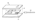
図1は、本実施の形態に係る回路基板の平面図の一例を示す図である。図2は、図1に示す回路基板のA−A線における、取り付け穴周辺部の基体の断面図の一例を示す図である。 FIG. 1 is a diagram showing an example of a plan view of a circuit board according to the present embodiment. FIG. 2 is a diagram showing an example of a cross-sectional view of a substrate around a mounting hole in line AA of the circuit board shown in FIG.
図1に示す回路基板1において、基体10は、コネクタC1の取り付け穴11を有し、基体10の外周に沿って縁1aに2列のビアホール12を有する。
In the
縁1aは、基体10における破線lの外側の領域を指し、ビアホール12を配置するために設けている。破線lの内側の領域を中央領域1bと呼ぶ。中央領域1bには、電源回路や信号処理回路などを集積し、取り付け穴11においてコネクタC1を固定する。
The
ビアホール12は、基体10を厚さ方向(図1の紙面の奥行方向)に貫通する貫通構造の孔(貫通孔)であり、隣り合う貫通孔との間隔Mが10mm以下になるように設ける。ビアホール12は、例えば、基体10に高速ドリルにより貫通孔を形成し、それから、貫通孔の内周面にメッキ処理によりメッキ層13を設ける。メッキ処理の工程は、従来工程であるため、ここでの詳しい説明を省略する。
The
図2に示すように基体10は、第1層L1〜第8層L8を有し、各層はそれぞれ、誘電体層P1、P2、・・・、P7により接着されている。ここでは多層構造の基体として8層構造のものを示しているが、一例であり、基体の層数は適宜変えても良い。
As shown in FIG. 2, the
基体10の中央領域1bにおいて、第2層L2、第4層L4、第7層L7がGNDベタパターン層である。第5層L5が電源ベタパターン層である。第1層L1、第3層L3、第6層L6、第8層L8が信号パターン層である。何れも導電材料(銅箔等)によりパターンが形成されている。
In the
基体10の縁1aには、全層(第1層L1、第2層L2、・・・、第8層L8)に導電材料(銅箔等)のGNDベタパターンN1、N2、・・・、N8を設けている。GNDベタパターンN1、N2、・・・、N8は、コネクタC1を配置した領域(配置領域)にも全層(第1層L1、第2層L2、・・・、第8層L8)に設けている。GNDベタパターンN1、N2、・・・、N8は、例えば従来のビルドアップ工法により各層の他の回路パターンと共に導電材料(銅箔等)をエッチングするなどして形成する。
On the
ビアホール12は、各層のGNDベタパターンを貫通する貫通構造を有し、その内周面にメッキ層13を有する。メッキ層13は、導電材料のメッキ(例えば銅など)の層であり、全層のGNDベタパターンN1、N2、・・・、N8を電気的に導通する機能を有する。
The
図3及び図4は、電子機器とハーネスとの接続形態の一例を示す図である。図3は、電子機器及びハーネスの模式図であり、図4は、電子機器の分解を示す模式図である。 3 and 4 are diagrams showing an example of a connection form between the electronic device and the harness. FIG. 3 is a schematic view of the electronic device and the harness, and FIG. 4 is a schematic view showing the disassembly of the electronic device.
図3に示すように、電子機器100のコネクタC1に対し、信号を伝送するハーネス101のプラグを接続する。コネクタC1は、図4に示すように、電子機器100の筐体内部に収容されている回路基板1の基体10の取り付け穴11(コネクタC1があるため図示されない)に、取り付け器具などを介してねじ等により締結されている。このコネクタC1にハーネス101の一端のプラグを接続し他方のプラグに別の回路基板(フレキシブルプリント基板等)を接続する。
As shown in FIG. 3, the plug of the
電子機器100は、一例として車載用の電子機器(車載カメラ等)とする。車載用の電子機器では、回路基板1の中央領域1bに車載用の所定目的のプリント配線が適用されている。なお、医療用や、航空宇宙用などの電子機器100であれば、回路基板1の中央領域1bに、それぞれに対応するプリント配線が適用されている。回路基板1は、車載用や、医療用や、航空宇宙用など、EMCの法規制が厳しく設定されている電子機器に対しての適用が可能である。
As an example, the
このように各層に設けたGNDベタパターンN1、N2、・・・、N8をビアホール12により電気的に接続することにより、コネクタC1の取り付け穴11にメッキを設けない設計においてもコネクタC1(具体的にはコネクタC1の金属カバー)と基体10のGNDとの接続インピーダンスが、従来構成のものと同等若しくはそれ以下に低くなり、コネクタC1へのノイズ電流の流れ込みを防止することが可能になる。従って、本実施の形態に係る回路基板1を使用した製品(電子機器)からの放射ノイズを許容値以内に抑えて、EMCの法規制を満たすことが可能になる。
By electrically connecting the GND solid patterns N1, N2, ..., N8 provided on each layer through the via holes 12, the connector C1 (specifically, even in a design in which the mounting holes 11 of the connector C1 are not plated. The connection impedance between the connector C1 (metal cover) and the GND of the
例えば、コネクタC1の取り付け穴11のメッキ層を無くしただけのものでは、1GHz以上の周波数、一例として1.6GHz帯が悪化し、車載用の電子機器についてEMC規格を満たさないものとなる。しかし、一例の回路基板1のように、GNDベタパターンN1、N2、・・・、N8とビアホール12とを追加し、ビアホール12にメッキ層13を設けることにより、その悪化が改善して、車載用の電子機器についてのEMC規格を満たすことが可能になる。
For example, if the plating layer of the mounting
(変形例1)
中央領域1bの回路面の集積密度を、内層配線の厚みをより厚くして配線幅を狭めることにより高くし、高集積化した中央領域1bの空いた領域を縁1a若しくはその一部として利用しても良い。
(Modification example 1)
The integration density of the circuit surface of the
図5は、変形例1に係る回路基板の断面図の一例を示す図である。当該断面図は、図1に示すA−A線の取り付け穴周辺部の位置に対応する変形例1の基体の断面図である。 FIG. 5 is a diagram showing an example of a cross-sectional view of the circuit board according to the first modification. The cross-sectional view is a cross-sectional view of the substrate of the modified example 1 corresponding to the position of the peripheral portion of the mounting hole of the line AA shown in FIG.
図5に示すように、変形例1に係る回路基板2の基体20において、電源層である第4層L4と第5層L5との各層の厚み(内層配線の厚み)をより厚くする。電源層の厚みをより厚くすることにより、電源層の断面を単位時間当たりに流れる電荷量が増加する。同じ電流を流す場合には、内部配線の配線幅を狭くすることができるため、電源層の配線面積を小さくすることができる。
As shown in FIG. 5, in the
電源層の配線面積が小さくなることにより、全体の層の面積も縮小することができ、ビアホール12を設ける場合において、回路基板2の面積を小さく抑えることが可能になる。
By reducing the wiring area of the power supply layer, the area of the entire layer can also be reduced, and when the via
(変形例2)
実施の形態では、ビアホール12と取り付け穴11との位置が取り付け穴11がビアホール12の列の内側(中央領域1b側)になる配置のものについて一例を示した。この配置は、逆つまり取り付け穴11がビアホール12の列の外側(縁1a側)になる配置であっても良い。
(Modification 2)
In the embodiment, an example is shown in which the positions of the via
図6及び図7は、変形例2に係る回路基板の説明図である。図6は、変形例2に係る回路基板の平面図の一例を示す図である。図7は、図6に示す回路基板のB−B線における、取り付け穴周辺部の基体の断面図の一例を示す図である。 6 and 7 are explanatory views of the circuit board according to the second modification. FIG. 6 is a diagram showing an example of a plan view of the circuit board according to the modified example 2. FIG. 7 is a diagram showing an example of a cross-sectional view of a substrate around a mounting hole in line BB of the circuit board shown in FIG.
図6に示すように、変形例2に係る回路基板3の基体30において、縁1aの端部に取り付け穴11を設ける。この場合、コネクタC1は図1に示す位置よりも縁1aの端部寄りに位置するため、コネクタC1にハーネス101(図4参照)を接続しやすくなる。
As shown in FIG. 6, in the
ビアホール12は、コネクタC1を迂回するようにコネクタC1の外周に沿って設ける。ここでは、中央領域1bの一部にビアホール12を設けた場合のものを一例として示しているが、電子機器が搭載可能であれば、縁1aを広めにとり、ビアホール12の迂回部分を縁1aに収めても良い。
The via
図6に示すような、ビアホール12を中央領域1bの一部に設ける必要がある場合であっても、ビアホール12又は各層のGNDベタパターンを、ビアホール12が各層のGNDベタパターンを電気的に接続する位置に設ける。例えば、中央領域1bにおいて、図6に示すビアホール12の位置の全層にGNDベタパターンを設ける。また、図6に示すビアホール12の位置において何れかの層に信号パターンなどがある場合は、その信号パターンを回避するようにビアホール12とGNDベタパターンとを設ける。
Even when it is necessary to provide the via
また、中央領域1bにおいて、何れかの層に信号パターンが含まれるなどの理由で、基体30に貫通孔を設けることができない場合は、該当する層の信号パターンなどを回避するように一部又は全ての層に配置をずらした非貫通孔を設ける。非貫通孔の内面にはメッキ層を設け、上の層のGNDベタパターンと下の層のGNDベタパターンとに電気的に接続する。これにより、全層のGNDベタパターンを各層に設けた非貫通孔のメッキ層により電気的に接続する。
Further, in the
実施の形態及び各変形例では、基体10、20、30に2列のビアホール12を設けた例を示したが、ビアホール12の配置のレイアウトや数などは適宜変形しても良い。例えば、取り付け穴11の配置間隔や深さや内周面の面積や、ビアホール12の径や配置間隔などに応じて、ビアホール12の列を3列にしたり、ビアホール12を取り付け穴11の近傍の領域のみに配置したり、数などを適宜変えて良い。
In the embodiment and each modification, an example in which two rows of via
ビアホール12の形状は、円柱形状以外に、適宜変形しても良い。例えば、すり鉢型の形状や多角柱の形状などとしても良い。
The shape of the via
1 回路基板
1a 縁
1b 中央領域
10 基体
11 取り付け穴
12 ビアホール
13 メッキ層
C1 コネクタ
L1〜L8 第1層〜第8層
N1〜N8 GNDベタパターン
P1〜P7 誘電体層
1
Claims (10)
前記基体は、
信号を伝送するハーネスを接続するコネクタの固定穴と、
複数の層に設けられたGNDベタパターンと、
前記複数の層に設けられた各GNDベタパターンを電気的に接続するビアホールと、
を有し、
前記複数の層のうちの電源層の各厚みがより厚く、
前記電源層に接する誘電体層の各厚みが前記電源層に接しない各誘電体層よりも薄い、
ことを特徴とする回路基板。 A circuit board having a multi-layered substrate
The substrate is
Fixing holes for connectors to connect harnesses that transmit signals,
The GND solid pattern provided on multiple layers and
A via hole that electrically connects each GND solid pattern provided in the plurality of layers,
Have a,
Each thickness of the power supply layer among the plurality of layers is thicker,
Each thickness of the dielectric layer in contact with the power supply layer is thinner than each dielectric layer not in contact with the power supply layer.
A circuit board characterized by that.
請求項1に記載の回路基板。 The GND solid pattern is contained in each layer of the substrate.
The circuit board according to claim 1.
請求項2に記載の回路基板。 The GND solid pattern is provided in each layer in the arrangement area of the connector fixed to the fixing hole and in the vicinity of the arrangement area.
The circuit board according to claim 2.
請求項3に記載の回路基板。 The via hole is provided in the vicinity of the arrangement area of the connector.
The circuit board according to claim 3.
請求項4に記載の回路基板。 The via hole is provided on the edge of the substrate.
The circuit board according to claim 4.
請求項5に記載の回路基板。 The via holes are provided in two rows.
The circuit board according to claim 5.
請求項6に記載の回路基板。 The via holes are provided in two rows along the outer circumference of the substrate.
The circuit board according to claim 6.
請求項7に記載の回路基板。 The via holes are provided at intervals of 10 mm or less so as not to overlap each other.
The circuit board according to claim 7.
請求項1乃至8の内の何れか一項に記載の回路基板。 The wiring width of the inner layer wiring of the substrate is narrowed by increasing the thickness.
The circuit board according to any one of claims 1 to 8.
請求項1乃至8の内の何れか一項に記載の回路基板。 The via hole has a penetrating structure penetrating the substrate.
The circuit board according to any one of claims 1 to 8.
Priority Applications (2)
| Application Number | Priority Date | Filing Date | Title |
|---|---|---|---|
| JP2017124666A JP6946776B2 (en) | 2017-06-26 | 2017-06-26 | Circuit board |
| US16/009,397 US10687414B2 (en) | 2017-06-26 | 2018-06-15 | Circuit board |
Applications Claiming Priority (1)
| Application Number | Priority Date | Filing Date | Title |
|---|---|---|---|
| JP2017124666A JP6946776B2 (en) | 2017-06-26 | 2017-06-26 | Circuit board |
Publications (2)
| Publication Number | Publication Date |
|---|---|
| JP2019009322A JP2019009322A (en) | 2019-01-17 |
| JP6946776B2 true JP6946776B2 (en) | 2021-10-06 |
Family
ID=64692998
Family Applications (1)
| Application Number | Title | Priority Date | Filing Date |
|---|---|---|---|
| JP2017124666A Active JP6946776B2 (en) | 2017-06-26 | 2017-06-26 | Circuit board |
Country Status (2)
| Country | Link |
|---|---|
| US (1) | US10687414B2 (en) |
| JP (1) | JP6946776B2 (en) |
Families Citing this family (3)
| Publication number | Priority date | Publication date | Assignee | Title |
|---|---|---|---|---|
| JP2020021808A (en) * | 2018-07-31 | 2020-02-06 | キヤノン株式会社 | Circuit board, and electronic apparatus with the circuit board |
| JP2021028934A (en) * | 2019-08-09 | 2021-02-25 | キヤノン株式会社 | Printed circuit board |
| KR20210031303A (en) * | 2019-09-11 | 2021-03-19 | 삼성전자주식회사 | An electronic device having a connector mounted on a circuit |
Family Cites Families (21)
| Publication number | Priority date | Publication date | Assignee | Title |
|---|---|---|---|---|
| JPH1154944A (en) * | 1997-08-07 | 1999-02-26 | Toshiba Corp | Circuit board |
| JP2000286587A (en) * | 1999-03-30 | 2000-10-13 | Matsushita Electric Ind Co Ltd | Electromagnetic shield structure at connector part with external cable |
| JP2001007456A (en) * | 1999-06-17 | 2001-01-12 | Toshiba Corp | Wiring circuit board |
| JP2001251063A (en) | 2000-03-06 | 2001-09-14 | Matsushita Electric Ind Co Ltd | Circuit board and television receiver using the same |
| JP2002222892A (en) * | 2001-01-26 | 2002-08-09 | Kyocera Corp | Multilayer wiring board |
| JP2004055988A (en) | 2002-07-23 | 2004-02-19 | Fujitsu Ltd | Information processing apparatus |
| JP3960178B2 (en) * | 2002-09-17 | 2007-08-15 | 株式会社デンソー | Multilayer printed circuit board |
| KR100717479B1 (en) * | 2002-10-31 | 2007-05-14 | 주식회사 아도반테스토 | Coupling unit for test apparatus |
| DE102004016146B4 (en) * | 2004-04-01 | 2006-09-14 | Epcos Ag | Electrical multilayer component |
| JP4551730B2 (en) * | 2004-10-15 | 2010-09-29 | イビデン株式会社 | Multilayer core substrate and manufacturing method thereof |
| US7355125B2 (en) * | 2005-11-17 | 2008-04-08 | International Business Machines Corporation | Printed circuit board and chip module |
| JP5070077B2 (en) | 2008-02-08 | 2012-11-07 | 株式会社リコー | Electrical board equipped with LSI, image forming control board, and image forming apparatus |
| WO2010114825A1 (en) * | 2009-03-30 | 2010-10-07 | Magna Mirrors Of America, Inc. | Electro-optic rearview mirror assembly for vehicle |
| KR101072591B1 (en) | 2009-08-10 | 2011-10-11 | 삼성전기주식회사 | Electromagnetic interference noise reduction board using electromagnetic bandgap structure |
| US8319116B2 (en) * | 2009-09-11 | 2012-11-27 | Oracle America, Inc. | Rib reinforcement of plated thru-holes |
| US8371316B2 (en) * | 2009-12-03 | 2013-02-12 | International Test Solutions, Inc. | Apparatuses, device, and methods for cleaning tester interface contact elements and support hardware |
| JP2012094843A (en) * | 2010-09-30 | 2012-05-17 | Incorporated Educational Institution Meisei | Circuit board, power supply structure, method for manufacturing circuit board, and method for manufacturing power supply structure |
| DE102011077206B4 (en) * | 2011-06-08 | 2019-01-31 | Zf Friedrichshafen Ag | Printed circuit board and control unit for a transmission of a vehicle with the printed circuit board |
| CN102496804A (en) * | 2011-11-22 | 2012-06-13 | 华为终端有限公司 | USB (universal serial bus) connector and electronic equipment |
| US8834182B2 (en) * | 2012-10-17 | 2014-09-16 | Microelectronics Assembly Technologies | Pierced flexible circuit and compression joint |
| DE102013211640A1 (en) * | 2013-06-20 | 2014-12-24 | Osram Opto Semiconductors Gmbh | Optoelectronic arrangement |
-
2017
- 2017-06-26 JP JP2017124666A patent/JP6946776B2/en active Active
-
2018
- 2018-06-15 US US16/009,397 patent/US10687414B2/en active Active
Also Published As
| Publication number | Publication date |
|---|---|
| JP2019009322A (en) | 2019-01-17 |
| US20180376581A1 (en) | 2018-12-27 |
| US10687414B2 (en) | 2020-06-16 |
Similar Documents
| Publication | Publication Date | Title |
|---|---|---|
| US6236572B1 (en) | Controlled impedance bus and method for a computer system | |
| US10741303B2 (en) | Transmission line, flat cable, and electronic device | |
| US8309863B2 (en) | Printed wiring board | |
| US7435912B1 (en) | Tailoring via impedance on a circuit board | |
| US7086869B1 (en) | Flexible cable interconnect with integrated EMC shielding | |
| EP2654387B1 (en) | Printed circuit board | |
| EP1945010B1 (en) | Multi-layer substrate and electronic device having the same | |
| KR100666224B1 (en) | Rigid flexible printed circuit board having openings | |
| CN104349575B (en) | Flexible PCB and preparation method thereof | |
| JP5983780B2 (en) | Printed wiring board, electronic device and wiring connection method | |
| JP6946776B2 (en) | Circuit board | |
| KR20170048575A (en) | Printed wiring board | |
| CN104040787A (en) | Printed circuit board with reduced cross-talk | |
| KR20070108258A (en) | Printed wiring board | |
| WO2008003021A2 (en) | Shielded via | |
| KR102447839B1 (en) | Circuit board and electronic device including the same | |
| CN109587942B (en) | Clearance size reduction for backdrilled differential vias | |
| US7186924B2 (en) | Dielectric structure for printed circuit board traces | |
| KR101888592B1 (en) | Flexible Printed Circuit and Method for Manufacturing The Same | |
| US7679005B2 (en) | Circuitized substrate with shielded signal lines and plated-thru-holes and method of making same, and electrical assembly and information handling system utilizing same | |
| US20030085055A1 (en) | Substrate design and process for reducing electromagnetic emission | |
| US20070181996A1 (en) | Circuit board | |
| US20070075418A1 (en) | Emi shielding device for pcb | |
| US20080165514A1 (en) | Printed circuit board | |
| US10729003B2 (en) | Anti-electromagnetic interference circuit board |
Legal Events
| Date | Code | Title | Description |
|---|---|---|---|
| A621 | Written request for application examination |
Free format text: JAPANESE INTERMEDIATE CODE: A621 Effective date: 20200226 |
|
| A977 | Report on retrieval |
Free format text: JAPANESE INTERMEDIATE CODE: A971007 Effective date: 20201224 |
|
| A131 | Notification of reasons for refusal |
Free format text: JAPANESE INTERMEDIATE CODE: A131 Effective date: 20210105 |
|
| A521 | Request for written amendment filed |
Free format text: JAPANESE INTERMEDIATE CODE: A523 Effective date: 20210303 |
|
| TRDD | Decision of grant or rejection written | ||
| A01 | Written decision to grant a patent or to grant a registration (utility model) |
Free format text: JAPANESE INTERMEDIATE CODE: A01 Effective date: 20210817 |
|
| A61 | First payment of annual fees (during grant procedure) |
Free format text: JAPANESE INTERMEDIATE CODE: A61 Effective date: 20210830 |
|
| R151 | Written notification of patent or utility model registration |
Ref document number: 6946776 Country of ref document: JP Free format text: JAPANESE INTERMEDIATE CODE: R151 |