JP6940495B2 - Equipment and methods for forming abrasive articles with the desired zeta potential - Google Patents
Equipment and methods for forming abrasive articles with the desired zeta potential Download PDFInfo
- Publication number
- JP6940495B2 JP6940495B2 JP2018521856A JP2018521856A JP6940495B2 JP 6940495 B2 JP6940495 B2 JP 6940495B2 JP 2018521856 A JP2018521856 A JP 2018521856A JP 2018521856 A JP2018521856 A JP 2018521856A JP 6940495 B2 JP6940495 B2 JP 6940495B2
- Authority
- JP
- Japan
- Prior art keywords
- polishing
- zeta potential
- feature
- polishing pad
- weight
- Prior art date
- Legal status (The legal status is an assumption and is not a legal conclusion. Google has not performed a legal analysis and makes no representation as to the accuracy of the status listed.)
- Active
Links
- 238000000034 method Methods 0.000 title description 72
- 238000005498 polishing Methods 0.000 claims description 658
- 239000000203 mixture Substances 0.000 claims description 170
- 239000000463 material Substances 0.000 claims description 160
- 239000000178 monomer Substances 0.000 claims description 48
- 239000002131 composite material Substances 0.000 claims description 41
- 239000002245 particle Substances 0.000 claims description 21
- 239000003607 modifier Substances 0.000 claims description 20
- 230000007935 neutral effect Effects 0.000 claims description 16
- 239000002861 polymer material Substances 0.000 claims description 13
- 125000002091 cationic group Chemical group 0.000 claims description 9
- 125000000129 anionic group Chemical group 0.000 claims description 6
- 239000010410 layer Substances 0.000 description 142
- 230000008569 process Effects 0.000 description 53
- 239000000976 ink Substances 0.000 description 49
- 239000000758 substrate Substances 0.000 description 45
- 238000001723 curing Methods 0.000 description 36
- 238000004519 manufacturing process Methods 0.000 description 30
- -1 fumed silica) Chemical compound 0.000 description 27
- 239000002002 slurry Substances 0.000 description 26
- 238000000151 deposition Methods 0.000 description 25
- 238000003860 storage Methods 0.000 description 25
- NIXOWILDQLNWCW-UHFFFAOYSA-M Acrylate Chemical compound [O-]C(=O)C=C NIXOWILDQLNWCW-UHFFFAOYSA-M 0.000 description 24
- 239000002243 precursor Substances 0.000 description 21
- 238000010146 3D printing Methods 0.000 description 17
- 238000013461 design Methods 0.000 description 16
- 239000000126 substance Substances 0.000 description 15
- 239000000654 additive Substances 0.000 description 13
- 238000007639 printing Methods 0.000 description 13
- 230000005855 radiation Effects 0.000 description 13
- 230000008021 deposition Effects 0.000 description 12
- 239000000243 solution Substances 0.000 description 12
- 229920001169 thermoplastic Polymers 0.000 description 11
- 239000003085 diluting agent Substances 0.000 description 10
- 229920000642 polymer Polymers 0.000 description 10
- 229920002635 polyurethane Polymers 0.000 description 10
- 239000004814 polyurethane Substances 0.000 description 10
- 150000001252 acrylic acid derivatives Chemical class 0.000 description 9
- 238000009472 formulation Methods 0.000 description 9
- 239000007788 liquid Substances 0.000 description 9
- 229910052751 metal Inorganic materials 0.000 description 9
- 239000002184 metal Substances 0.000 description 9
- 229920000728 polyester Polymers 0.000 description 9
- VYPSYNLAJGMNEJ-UHFFFAOYSA-N Silicium dioxide Chemical compound O=[Si]=O VYPSYNLAJGMNEJ-UHFFFAOYSA-N 0.000 description 8
- 239000012530 fluid Substances 0.000 description 8
- 238000007517 polishing process Methods 0.000 description 8
- 229920001577 copolymer Chemical class 0.000 description 7
- 230000015654 memory Effects 0.000 description 7
- 238000012545 processing Methods 0.000 description 7
- 230000000996 additive effect Effects 0.000 description 6
- 239000000356 contaminant Substances 0.000 description 6
- 239000003999 initiator Substances 0.000 description 6
- 239000010954 inorganic particle Substances 0.000 description 6
- 239000012705 liquid precursor Substances 0.000 description 6
- 239000011146 organic particle Substances 0.000 description 6
- 239000004721 Polyphenylene oxide Substances 0.000 description 5
- 239000006227 byproduct Substances 0.000 description 5
- 238000004140 cleaning Methods 0.000 description 5
- 230000003287 optical effect Effects 0.000 description 5
- 229920003229 poly(methyl methacrylate) Polymers 0.000 description 5
- 229920000570 polyether Polymers 0.000 description 5
- 239000004926 polymethyl methacrylate Substances 0.000 description 5
- 239000000843 powder Substances 0.000 description 5
- 239000007787 solid Substances 0.000 description 5
- 239000004696 Poly ether ether ketone Substances 0.000 description 4
- 239000004952 Polyamide Substances 0.000 description 4
- 239000004697 Polyetherimide Substances 0.000 description 4
- NJSSICCENMLTKO-HRCBOCMUSA-N [(1r,2s,4r,5r)-3-hydroxy-4-(4-methylphenyl)sulfonyloxy-6,8-dioxabicyclo[3.2.1]octan-2-yl] 4-methylbenzenesulfonate Chemical compound C1=CC(C)=CC=C1S(=O)(=O)O[C@H]1C(O)[C@@H](OS(=O)(=O)C=2C=CC(C)=CC=2)[C@@H]2OC[C@H]1O2 NJSSICCENMLTKO-HRCBOCMUSA-N 0.000 description 4
- 239000004676 acrylonitrile butadiene styrene Substances 0.000 description 4
- PNEYBMLMFCGWSK-UHFFFAOYSA-N aluminium oxide Inorganic materials [O-2].[O-2].[O-2].[Al+3].[Al+3] PNEYBMLMFCGWSK-UHFFFAOYSA-N 0.000 description 4
- 230000001588 bifunctional effect Effects 0.000 description 4
- 230000015572 biosynthetic process Effects 0.000 description 4
- 238000005266 casting Methods 0.000 description 4
- 238000011960 computer-aided design Methods 0.000 description 4
- 230000007547 defect Effects 0.000 description 4
- 239000008240 homogeneous mixture Substances 0.000 description 4
- 230000033001 locomotion Effects 0.000 description 4
- 238000000465 moulding Methods 0.000 description 4
- 229920002647 polyamide Polymers 0.000 description 4
- 229920002530 polyetherether ketone Polymers 0.000 description 4
- 229920001601 polyetherimide Polymers 0.000 description 4
- 238000009877 rendering Methods 0.000 description 4
- 239000007779 soft material Substances 0.000 description 4
- 230000007704 transition Effects 0.000 description 4
- 239000004593 Epoxy Substances 0.000 description 3
- JOYRKODLDBILNP-UHFFFAOYSA-N Ethyl urethane Chemical compound CCOC(N)=O JOYRKODLDBILNP-UHFFFAOYSA-N 0.000 description 3
- LYCAIKOWRPUZTN-UHFFFAOYSA-N Ethylene glycol Chemical compound OCCO LYCAIKOWRPUZTN-UHFFFAOYSA-N 0.000 description 3
- 229920000877 Melamine resin Polymers 0.000 description 3
- 229930040373 Paraformaldehyde Natural products 0.000 description 3
- 239000004642 Polyimide Substances 0.000 description 3
- 239000004743 Polypropylene Substances 0.000 description 3
- 239000004793 Polystyrene Substances 0.000 description 3
- NIXOWILDQLNWCW-UHFFFAOYSA-N acrylic acid group Chemical group C(C=C)(=O)O NIXOWILDQLNWCW-UHFFFAOYSA-N 0.000 description 3
- 230000008901 benefit Effects 0.000 description 3
- 230000005540 biological transmission Effects 0.000 description 3
- 239000013590 bulk material Substances 0.000 description 3
- CETPSERCERDGAM-UHFFFAOYSA-N ceric oxide Chemical compound O=[Ce]=O CETPSERCERDGAM-UHFFFAOYSA-N 0.000 description 3
- 229910000422 cerium(IV) oxide Inorganic materials 0.000 description 3
- 230000003750 conditioning effect Effects 0.000 description 3
- 238000005137 deposition process Methods 0.000 description 3
- 238000001514 detection method Methods 0.000 description 3
- 125000004386 diacrylate group Chemical group 0.000 description 3
- 238000010586 diagram Methods 0.000 description 3
- 125000003700 epoxy group Chemical group 0.000 description 3
- UHESRSKEBRADOO-UHFFFAOYSA-N ethyl carbamate;prop-2-enoic acid Chemical compound OC(=O)C=C.CCOC(N)=O UHESRSKEBRADOO-UHFFFAOYSA-N 0.000 description 3
- 239000006260 foam Substances 0.000 description 3
- 230000006870 function Effects 0.000 description 3
- 229920001519 homopolymer Polymers 0.000 description 3
- 229930195733 hydrocarbon Natural products 0.000 description 3
- 150000002430 hydrocarbons Chemical class 0.000 description 3
- 150000002500 ions Chemical class 0.000 description 3
- JDSHMPZPIAZGSV-UHFFFAOYSA-N melamine Chemical compound NC1=NC(N)=NC(N)=N1 JDSHMPZPIAZGSV-UHFFFAOYSA-N 0.000 description 3
- 150000002739 metals Chemical class 0.000 description 3
- YDKNBNOOCSNPNS-UHFFFAOYSA-N methyl 1,3-benzoxazole-2-carboxylate Chemical compound C1=CC=C2OC(C(=O)OC)=NC2=C1 YDKNBNOOCSNPNS-UHFFFAOYSA-N 0.000 description 3
- 229920002493 poly(chlorotrifluoroethylene) Polymers 0.000 description 3
- 229920002492 poly(sulfone) Polymers 0.000 description 3
- 229920002239 polyacrylonitrile Polymers 0.000 description 3
- 239000004417 polycarbonate Substances 0.000 description 3
- 229920000515 polycarbonate Polymers 0.000 description 3
- 239000005023 polychlorotrifluoroethylene (PCTFE) polymer Substances 0.000 description 3
- 229920001721 polyimide Polymers 0.000 description 3
- 229920006324 polyoxymethylene Polymers 0.000 description 3
- 229920001155 polypropylene Polymers 0.000 description 3
- 229920001296 polysiloxane Polymers 0.000 description 3
- 229920002223 polystyrene Polymers 0.000 description 3
- 239000004810 polytetrafluoroethylene Substances 0.000 description 3
- 229920001343 polytetrafluoroethylene Polymers 0.000 description 3
- 229920002689 polyvinyl acetate Polymers 0.000 description 3
- 239000011118 polyvinyl acetate Substances 0.000 description 3
- 239000000377 silicon dioxide Substances 0.000 description 3
- 229920001187 thermosetting polymer Polymers 0.000 description 3
- 239000004634 thermosetting polymer Substances 0.000 description 3
- LEJBBGNFPAFPKQ-UHFFFAOYSA-N 2-(2-prop-2-enoyloxyethoxy)ethyl prop-2-enoate Chemical compound C=CC(=O)OCCOCCOC(=O)C=C LEJBBGNFPAFPKQ-UHFFFAOYSA-N 0.000 description 2
- INQDDHNZXOAFFD-UHFFFAOYSA-N 2-[2-(2-prop-2-enoyloxyethoxy)ethoxy]ethyl prop-2-enoate Chemical compound C=CC(=O)OCCOCCOCCOC(=O)C=C INQDDHNZXOAFFD-UHFFFAOYSA-N 0.000 description 2
- HCLJOFJIQIJXHS-UHFFFAOYSA-N 2-[2-[2-(2-prop-2-enoyloxyethoxy)ethoxy]ethoxy]ethyl prop-2-enoate Chemical compound C=CC(=O)OCCOCCOCCOCCOC(=O)C=C HCLJOFJIQIJXHS-UHFFFAOYSA-N 0.000 description 2
- XMLYCEVDHLAQEL-UHFFFAOYSA-N 2-hydroxy-2-methyl-1-phenylpropan-1-one Chemical compound CC(C)(O)C(=O)C1=CC=CC=C1 XMLYCEVDHLAQEL-UHFFFAOYSA-N 0.000 description 2
- RZVINYQDSSQUKO-UHFFFAOYSA-N 2-phenoxyethyl prop-2-enoate Chemical compound C=CC(=O)OCCOC1=CC=CC=C1 RZVINYQDSSQUKO-UHFFFAOYSA-N 0.000 description 2
- KGIGUEBEKRSTEW-UHFFFAOYSA-N 2-vinylpyridine Chemical compound C=CC1=CC=CC=N1 KGIGUEBEKRSTEW-UHFFFAOYSA-N 0.000 description 2
- JHWGFJBTMHEZME-UHFFFAOYSA-N 4-prop-2-enoyloxybutyl prop-2-enoate Chemical compound C=CC(=O)OCCCCOC(=O)C=C JHWGFJBTMHEZME-UHFFFAOYSA-N 0.000 description 2
- FIHBHSQYSYVZQE-UHFFFAOYSA-N 6-prop-2-enoyloxyhexyl prop-2-enoate Chemical compound C=CC(=O)OCCCCCCOC(=O)C=C FIHBHSQYSYVZQE-UHFFFAOYSA-N 0.000 description 2
- NLXLAEXVIDQMFP-UHFFFAOYSA-N Ammonia chloride Chemical compound [NH4+].[Cl-] NLXLAEXVIDQMFP-UHFFFAOYSA-N 0.000 description 2
- VEXZGXHMUGYJMC-UHFFFAOYSA-M Chloride anion Chemical compound [Cl-] VEXZGXHMUGYJMC-UHFFFAOYSA-M 0.000 description 2
- 229920002943 EPDM rubber Polymers 0.000 description 2
- WHNWPMSKXPGLAX-UHFFFAOYSA-N N-Vinyl-2-pyrrolidone Chemical compound C=CN1CCCC1=O WHNWPMSKXPGLAX-UHFFFAOYSA-N 0.000 description 2
- 229920002845 Poly(methacrylic acid) Polymers 0.000 description 2
- 239000004695 Polyether sulfone Substances 0.000 description 2
- 229920002873 Polyethylenimine Polymers 0.000 description 2
- PPBRXRYQALVLMV-UHFFFAOYSA-N Styrene Chemical compound C=CC1=CC=CC=C1 PPBRXRYQALVLMV-UHFFFAOYSA-N 0.000 description 2
- 238000003848 UV Light-Curing Methods 0.000 description 2
- MCMNRKCIXSYSNV-UHFFFAOYSA-N Zirconium dioxide Chemical compound O=[Zr]=O MCMNRKCIXSYSNV-UHFFFAOYSA-N 0.000 description 2
- 125000003118 aryl group Chemical group 0.000 description 2
- 230000001174 ascending effect Effects 0.000 description 2
- QVGXLLKOCUKJST-UHFFFAOYSA-N atomic oxygen Chemical compound [O] QVGXLLKOCUKJST-UHFFFAOYSA-N 0.000 description 2
- 239000011230 binding agent Substances 0.000 description 2
- IISBACLAFKSPIT-UHFFFAOYSA-N bisphenol A Chemical compound C=1C=C(O)C=CC=1C(C)(C)C1=CC=C(O)C=C1 IISBACLAFKSPIT-UHFFFAOYSA-N 0.000 description 2
- 239000000919 ceramic Substances 0.000 description 2
- 230000008859 change Effects 0.000 description 2
- 238000006243 chemical reaction Methods 0.000 description 2
- 239000003795 chemical substances by application Substances 0.000 description 2
- 150000002009 diols Chemical class 0.000 description 2
- 238000009826 distribution Methods 0.000 description 2
- 230000000694 effects Effects 0.000 description 2
- 125000001495 ethyl group Chemical group [H]C([H])([H])C([H])([H])* 0.000 description 2
- 230000009477 glass transition Effects 0.000 description 2
- 238000010438 heat treatment Methods 0.000 description 2
- WGCNASOHLSPBMP-UHFFFAOYSA-N hydroxyacetaldehyde Natural products OCC=O WGCNASOHLSPBMP-UHFFFAOYSA-N 0.000 description 2
- 238000002347 injection Methods 0.000 description 2
- 239000007924 injection Substances 0.000 description 2
- 229910000765 intermetallic Inorganic materials 0.000 description 2
- PBOSTUDLECTMNL-UHFFFAOYSA-N lauryl acrylate Chemical compound CCCCCCCCCCCCOC(=O)C=C PBOSTUDLECTMNL-UHFFFAOYSA-N 0.000 description 2
- 230000013011 mating Effects 0.000 description 2
- 229910021645 metal ion Inorganic materials 0.000 description 2
- 229910044991 metal oxide Inorganic materials 0.000 description 2
- 150000004706 metal oxides Chemical class 0.000 description 2
- 238000002156 mixing Methods 0.000 description 2
- 239000001301 oxygen Substances 0.000 description 2
- 229910052760 oxygen Inorganic materials 0.000 description 2
- 238000005192 partition Methods 0.000 description 2
- 125000001997 phenyl group Chemical group [H]C1=C([H])C([H])=C(*)C([H])=C1[H] 0.000 description 2
- 229920001084 poly(chloroprene) Polymers 0.000 description 2
- 229920002401 polyacrylamide Polymers 0.000 description 2
- 229920000647 polyepoxide Polymers 0.000 description 2
- 229920006393 polyether sulfone Polymers 0.000 description 2
- 229920001223 polyethylene glycol Polymers 0.000 description 2
- 229920001444 polymaleic acid Polymers 0.000 description 2
- 238000006116 polymerization reaction Methods 0.000 description 2
- 239000000047 product Substances 0.000 description 2
- 230000009467 reduction Effects 0.000 description 2
- 229920005989 resin Polymers 0.000 description 2
- 239000011347 resin Substances 0.000 description 2
- 230000000717 retained effect Effects 0.000 description 2
- 239000004065 semiconductor Substances 0.000 description 2
- 238000005245 sintering Methods 0.000 description 2
- 239000002904 solvent Substances 0.000 description 2
- 239000004094 surface-active agent Substances 0.000 description 2
- 238000012546 transfer Methods 0.000 description 2
- RRHXZLALVWBDKH-UHFFFAOYSA-M trimethyl-[2-(2-methylprop-2-enoyloxy)ethyl]azanium;chloride Chemical compound [Cl-].CC(=C)C(=O)OCC[N+](C)(C)C RRHXZLALVWBDKH-UHFFFAOYSA-M 0.000 description 2
- 125000000391 vinyl group Chemical group [H]C([*])=C([H])[H] 0.000 description 2
- 229920002554 vinyl polymer Polymers 0.000 description 2
- XPEMPJFPRCHICU-UHFFFAOYSA-N (1-tert-butylcyclohexyl) prop-2-enoate Chemical compound C=CC(=O)OC1(C(C)(C)C)CCCCC1 XPEMPJFPRCHICU-UHFFFAOYSA-N 0.000 description 1
- HHQAGBQXOWLTLL-UHFFFAOYSA-N (2-hydroxy-3-phenoxypropyl) prop-2-enoate Chemical compound C=CC(=O)OCC(O)COC1=CC=CC=C1 HHQAGBQXOWLTLL-UHFFFAOYSA-N 0.000 description 1
- PSGCQDPCAWOCSH-UHFFFAOYSA-N (4,7,7-trimethyl-3-bicyclo[2.2.1]heptanyl) prop-2-enoate Chemical compound C1CC2(C)C(OC(=O)C=C)CC1C2(C)C PSGCQDPCAWOCSH-UHFFFAOYSA-N 0.000 description 1
- MYWOJODOMFBVCB-UHFFFAOYSA-N 1,2,6-trimethylphenanthrene Chemical compound CC1=CC=C2C3=CC(C)=CC=C3C=CC2=C1C MYWOJODOMFBVCB-UHFFFAOYSA-N 0.000 description 1
- VDYWHVQKENANGY-UHFFFAOYSA-N 1,3-Butyleneglycol dimethacrylate Chemical compound CC(=C)C(=O)OC(C)CCOC(=O)C(C)=C VDYWHVQKENANGY-UHFFFAOYSA-N 0.000 description 1
- ZDQNWDNMNKSMHI-UHFFFAOYSA-N 1-[2-(2-prop-2-enoyloxypropoxy)propoxy]propan-2-yl prop-2-enoate Chemical compound C=CC(=O)OC(C)COC(C)COCC(C)OC(=O)C=C ZDQNWDNMNKSMHI-UHFFFAOYSA-N 0.000 description 1
- OZFIGURLAJSLIR-UHFFFAOYSA-N 1-ethenyl-2h-pyridine Chemical compound C=CN1CC=CC=C1 OZFIGURLAJSLIR-UHFFFAOYSA-N 0.000 description 1
- OBNIRVVPHSLTEP-UHFFFAOYSA-N 1-ethoxy-2-(2-hydroxyethoxy)ethanol;prop-2-enoic acid Chemical compound OC(=O)C=C.CCOC(O)COCCO OBNIRVVPHSLTEP-UHFFFAOYSA-N 0.000 description 1
- 239000012956 1-hydroxycyclohexylphenyl-ketone Substances 0.000 description 1
- OAOWPYJFWWOMNQ-UHFFFAOYSA-N 1-methoxypropane-1,2-diol;prop-2-enoic acid Chemical compound OC(=O)C=C.COC(O)C(C)O OAOWPYJFWWOMNQ-UHFFFAOYSA-N 0.000 description 1
- OEURXIFGOPBMJF-UHFFFAOYSA-N 1-o-(2-hydroxyethyl) 2-o-(2-prop-2-enoyloxyethyl) benzene-1,2-dicarboxylate Chemical compound OCCOC(=O)C1=CC=CC=C1C(=O)OCCOC(=O)C=C OEURXIFGOPBMJF-UHFFFAOYSA-N 0.000 description 1
- VOBUAPTXJKMNCT-UHFFFAOYSA-N 1-prop-2-enoyloxyhexyl prop-2-enoate Chemical compound CCCCCC(OC(=O)C=C)OC(=O)C=C VOBUAPTXJKMNCT-UHFFFAOYSA-N 0.000 description 1
- YIKSHDNOAYSSPX-UHFFFAOYSA-N 1-propan-2-ylthioxanthen-9-one Chemical compound S1C2=CC=CC=C2C(=O)C2=C1C=CC=C2C(C)C YIKSHDNOAYSSPX-UHFFFAOYSA-N 0.000 description 1
- STFXXRRQKFUYEU-UHFFFAOYSA-N 16-methylheptadecyl prop-2-enoate Chemical class CC(C)CCCCCCCCCCCCCCCOC(=O)C=C STFXXRRQKFUYEU-UHFFFAOYSA-N 0.000 description 1
- KWVGIHKZDCUPEU-UHFFFAOYSA-N 2,2-dimethoxy-2-phenylacetophenone Chemical compound C=1C=CC=CC=1C(OC)(OC)C(=O)C1=CC=CC=C1 KWVGIHKZDCUPEU-UHFFFAOYSA-N 0.000 description 1
- FTALTLPZDVFJSS-UHFFFAOYSA-N 2-(2-ethoxyethoxy)ethyl prop-2-enoate Chemical compound CCOCCOCCOC(=O)C=C FTALTLPZDVFJSS-UHFFFAOYSA-N 0.000 description 1
- CMCLUJRFBZBVSW-UHFFFAOYSA-N 2-(2-hydroxyethoxy)-1-methoxyethanol;prop-2-enoic acid Chemical compound OC(=O)C=C.COC(O)COCCO CMCLUJRFBZBVSW-UHFFFAOYSA-N 0.000 description 1
- UECGJSXCVLTIMQ-UHFFFAOYSA-N 2-(2-prop-2-enoyloxyethoxycarbonyl)cyclohexane-1-carboxylic acid Chemical compound OC(=O)C1CCCCC1C(=O)OCCOC(=O)C=C UECGJSXCVLTIMQ-UHFFFAOYSA-N 0.000 description 1
- IPDYIFGHKYLTOM-UHFFFAOYSA-N 2-(2-prop-2-enoyloxypropoxy)propyl prop-2-enoate Chemical class C=CC(=O)OCC(C)OCC(C)OC(=O)C=C IPDYIFGHKYLTOM-UHFFFAOYSA-N 0.000 description 1
- FLKHVLRENDBIDB-UHFFFAOYSA-N 2-(butylcarbamoyloxy)ethyl prop-2-enoate Chemical compound CCCCNC(=O)OCCOC(=O)C=C FLKHVLRENDBIDB-UHFFFAOYSA-N 0.000 description 1
- WMYINDVYGQKYMI-UHFFFAOYSA-N 2-[2,2-bis(hydroxymethyl)butoxymethyl]-2-ethylpropane-1,3-diol Chemical compound CCC(CO)(CO)COCC(CC)(CO)CO WMYINDVYGQKYMI-UHFFFAOYSA-N 0.000 description 1
- XFCMNSHQOZQILR-UHFFFAOYSA-N 2-[2-(2-methylprop-2-enoyloxy)ethoxy]ethyl 2-methylprop-2-enoate Chemical class CC(=C)C(=O)OCCOCCOC(=O)C(C)=C XFCMNSHQOZQILR-UHFFFAOYSA-N 0.000 description 1
- LJRSZGKUUZPHEB-UHFFFAOYSA-N 2-[2-(2-prop-2-enoyloxypropoxy)propoxy]propyl prop-2-enoate Chemical class C=CC(=O)OC(C)COC(C)COC(C)COC(=O)C=C LJRSZGKUUZPHEB-UHFFFAOYSA-N 0.000 description 1
- HWSSEYVMGDIFMH-UHFFFAOYSA-N 2-[2-[2-(2-methylprop-2-enoyloxy)ethoxy]ethoxy]ethyl 2-methylprop-2-enoate Chemical class CC(=C)C(=O)OCCOCCOCCOC(=O)C(C)=C HWSSEYVMGDIFMH-UHFFFAOYSA-N 0.000 description 1
- QPXVRLXJHPTCPW-UHFFFAOYSA-N 2-hydroxy-2-methyl-1-(4-propan-2-ylphenyl)propan-1-one Chemical compound CC(C)C1=CC=C(C(=O)C(C)(C)O)C=C1 QPXVRLXJHPTCPW-UHFFFAOYSA-N 0.000 description 1
- NJRHMGPRPPEGQL-UHFFFAOYSA-N 2-hydroxybutyl prop-2-enoate Chemical class CCC(O)COC(=O)C=C NJRHMGPRPPEGQL-UHFFFAOYSA-N 0.000 description 1
- 229940095095 2-hydroxyethyl acrylate Drugs 0.000 description 1
- OMIGHNLMNHATMP-UHFFFAOYSA-N 2-hydroxyethyl prop-2-enoate Chemical compound OCCOC(=O)C=C OMIGHNLMNHATMP-UHFFFAOYSA-N 0.000 description 1
- GWZMWHWAWHPNHN-UHFFFAOYSA-N 2-hydroxypropyl prop-2-enoate Chemical compound CC(O)COC(=O)C=C GWZMWHWAWHPNHN-UHFFFAOYSA-N 0.000 description 1
- LWRBVKNFOYUCNP-UHFFFAOYSA-N 2-methyl-1-(4-methylsulfanylphenyl)-2-morpholin-4-ylpropan-1-one Chemical compound C1=CC(SC)=CC=C1C(=O)C(C)(C)N1CCOCC1 LWRBVKNFOYUCNP-UHFFFAOYSA-N 0.000 description 1
- DCBJXJOKADGNAA-UHFFFAOYSA-N 2-methyl-1-[6-(2-methyl-2-morpholin-4-ylpropanoyl)-9-octylcarbazol-3-yl]-2-morpholin-4-ylpropan-1-one Chemical compound C=1C=C2N(CCCCCCCC)C3=CC=C(C(=O)C(C)(C)N4CCOCC4)C=C3C2=CC=1C(=O)C(C)(C)N1CCOCC1 DCBJXJOKADGNAA-UHFFFAOYSA-N 0.000 description 1
- CEXQWAAGPPNOQF-UHFFFAOYSA-N 2-phenoxyethyl 2-methylprop-2-enoate Chemical compound CC(=C)C(=O)OCCOC1=CC=CC=C1 CEXQWAAGPPNOQF-UHFFFAOYSA-N 0.000 description 1
- RDFQSFOGKVZWKF-UHFFFAOYSA-N 3-hydroxy-2,2-dimethylpropanoic acid Chemical compound OCC(C)(C)C(O)=O RDFQSFOGKVZWKF-UHFFFAOYSA-N 0.000 description 1
- ZVYGIPWYVVJFRW-UHFFFAOYSA-N 3-methylbutyl prop-2-enoate Chemical class CC(C)CCOC(=O)C=C ZVYGIPWYVVJFRW-UHFFFAOYSA-N 0.000 description 1
- FQMIAEWUVYWVNB-UHFFFAOYSA-N 3-prop-2-enoyloxybutyl prop-2-enoate Chemical compound C=CC(=O)OC(C)CCOC(=O)C=C FQMIAEWUVYWVNB-UHFFFAOYSA-N 0.000 description 1
- XOJWAAUYNWGQAU-UHFFFAOYSA-N 4-(2-methylprop-2-enoyloxy)butyl 2-methylprop-2-enoate Chemical compound CC(=C)C(=O)OCCCCOC(=O)C(C)=C XOJWAAUYNWGQAU-UHFFFAOYSA-N 0.000 description 1
- KFDVPJUYSDEJTH-UHFFFAOYSA-N 4-ethenylpyridine Chemical compound C=CC1=CC=NC=C1 KFDVPJUYSDEJTH-UHFFFAOYSA-N 0.000 description 1
- UZDMJPAQQFSMMV-UHFFFAOYSA-N 4-oxo-4-(2-prop-2-enoyloxyethoxy)butanoic acid Chemical compound OC(=O)CCC(=O)OCCOC(=O)C=C UZDMJPAQQFSMMV-UHFFFAOYSA-N 0.000 description 1
- WIYVVIUBKNTNKG-UHFFFAOYSA-N 6,7-dimethoxy-3,4-dihydronaphthalene-2-carboxylic acid Chemical compound C1CC(C(O)=O)=CC2=C1C=C(OC)C(OC)=C2 WIYVVIUBKNTNKG-UHFFFAOYSA-N 0.000 description 1
- SAPGBCWOQLHKKZ-UHFFFAOYSA-N 6-(2-methylprop-2-enoyloxy)hexyl 2-methylprop-2-enoate Chemical compound CC(=C)C(=O)OCCCCCCOC(=O)C(C)=C SAPGBCWOQLHKKZ-UHFFFAOYSA-N 0.000 description 1
- JTHZUSWLNCPZLX-UHFFFAOYSA-N 6-fluoro-3-methyl-2h-indazole Chemical compound FC1=CC=C2C(C)=NNC2=C1 JTHZUSWLNCPZLX-UHFFFAOYSA-N 0.000 description 1
- DXPPIEDUBFUSEZ-UHFFFAOYSA-N 6-methylheptyl prop-2-enoate Chemical compound CC(C)CCCCCOC(=O)C=C DXPPIEDUBFUSEZ-UHFFFAOYSA-N 0.000 description 1
- COCLLEMEIJQBAG-UHFFFAOYSA-N 8-methylnonyl 2-methylprop-2-enoate Chemical compound CC(C)CCCCCCCOC(=O)C(C)=C COCLLEMEIJQBAG-UHFFFAOYSA-N 0.000 description 1
- LVGFPWDANALGOY-UHFFFAOYSA-N 8-methylnonyl prop-2-enoate Chemical compound CC(C)CCCCCCCOC(=O)C=C LVGFPWDANALGOY-UHFFFAOYSA-N 0.000 description 1
- PGDIJTMOHORACQ-UHFFFAOYSA-N 9-prop-2-enoyloxynonyl prop-2-enoate Chemical compound C=CC(=O)OCCCCCCCCCOC(=O)C=C PGDIJTMOHORACQ-UHFFFAOYSA-N 0.000 description 1
- HRPVXLWXLXDGHG-UHFFFAOYSA-N Acrylamide Chemical compound NC(=O)C=C HRPVXLWXLXDGHG-UHFFFAOYSA-N 0.000 description 1
- 229910018072 Al 2 O 3 Inorganic materials 0.000 description 1
- 238000005033 Fourier transform infrared spectroscopy Methods 0.000 description 1
- 244000043261 Hevea brasiliensis Species 0.000 description 1
- CERQOIWHTDAKMF-UHFFFAOYSA-M Methacrylate Chemical compound CC(=C)C([O-])=O CERQOIWHTDAKMF-UHFFFAOYSA-M 0.000 description 1
- 229920000707 Poly(2-dimethylamino)ethyl methacrylate) methyl chloride Polymers 0.000 description 1
- 239000002202 Polyethylene glycol Substances 0.000 description 1
- 229920000265 Polyparaphenylene Polymers 0.000 description 1
- XUIMIQQOPSSXEZ-UHFFFAOYSA-N Silicon Chemical compound [Si] XUIMIQQOPSSXEZ-UHFFFAOYSA-N 0.000 description 1
- 229920002125 Sokalan® Polymers 0.000 description 1
- UCKMPCXJQFINFW-UHFFFAOYSA-N Sulphide Chemical compound [S-2] UCKMPCXJQFINFW-UHFFFAOYSA-N 0.000 description 1
- LCXXNKZQVOXMEH-UHFFFAOYSA-N Tetrahydrofurfuryl methacrylate Chemical class CC(=C)C(=O)OCC1CCCO1 LCXXNKZQVOXMEH-UHFFFAOYSA-N 0.000 description 1
- 241001193851 Zeta Species 0.000 description 1
- FIDYXZSJZSCJES-UHFFFAOYSA-N [(2,6-dimethoxybenzoyl)-(2,4,6-trimethylphenyl)phosphoryl]-(2,6-dimethoxyphenyl)methanone Chemical compound COC1=CC=CC(OC)=C1C(=O)P(=O)(C=1C(=CC(C)=CC=1C)C)C(=O)C1=C(OC)C=CC=C1OC FIDYXZSJZSCJES-UHFFFAOYSA-N 0.000 description 1
- HVVWZTWDBSEWIH-UHFFFAOYSA-N [2-(hydroxymethyl)-3-prop-2-enoyloxy-2-(prop-2-enoyloxymethyl)propyl] prop-2-enoate Chemical compound C=CC(=O)OCC(CO)(COC(=O)C=C)COC(=O)C=C HVVWZTWDBSEWIH-UHFFFAOYSA-N 0.000 description 1
- MPIAGWXWVAHQBB-UHFFFAOYSA-N [3-prop-2-enoyloxy-2-[[3-prop-2-enoyloxy-2,2-bis(prop-2-enoyloxymethyl)propoxy]methyl]-2-(prop-2-enoyloxymethyl)propyl] prop-2-enoate Chemical compound C=CC(=O)OCC(COC(=O)C=C)(COC(=O)C=C)COCC(COC(=O)C=C)(COC(=O)C=C)COC(=O)C=C MPIAGWXWVAHQBB-UHFFFAOYSA-N 0.000 description 1
- 238000010521 absorption reaction Methods 0.000 description 1
- 239000002253 acid Substances 0.000 description 1
- 150000007513 acids Chemical class 0.000 description 1
- 150000003926 acrylamides Chemical class 0.000 description 1
- 238000004220 aggregation Methods 0.000 description 1
- 230000002776 aggregation Effects 0.000 description 1
- 125000001931 aliphatic group Chemical group 0.000 description 1
- 125000005250 alkyl acrylate group Chemical group 0.000 description 1
- 150000001412 amines Chemical class 0.000 description 1
- 125000003277 amino group Chemical group 0.000 description 1
- 235000019270 ammonium chloride Nutrition 0.000 description 1
- QGZKDVFQNNGYKY-UHFFFAOYSA-O ammonium group Chemical group [NH4+] QGZKDVFQNNGYKY-UHFFFAOYSA-O 0.000 description 1
- 229920006318 anionic polymer Polymers 0.000 description 1
- 150000001450 anions Chemical class 0.000 description 1
- 238000003491 array Methods 0.000 description 1
- 239000012298 atmosphere Substances 0.000 description 1
- JUPQTSLXMOCDHR-UHFFFAOYSA-N benzene-1,4-diol;bis(4-fluorophenyl)methanone Chemical compound OC1=CC=C(O)C=C1.C1=CC(F)=CC=C1C(=O)C1=CC=C(F)C=C1 JUPQTSLXMOCDHR-UHFFFAOYSA-N 0.000 description 1
- RWCCWEUUXYIKHB-UHFFFAOYSA-N benzophenone Chemical compound C=1C=CC=CC=1C(=O)C1=CC=CC=C1 RWCCWEUUXYIKHB-UHFFFAOYSA-N 0.000 description 1
- 239000012965 benzophenone Substances 0.000 description 1
- MQDJYUACMFCOFT-UHFFFAOYSA-N bis[2-(1-hydroxycyclohexyl)phenyl]methanone Chemical compound C=1C=CC=C(C(=O)C=2C(=CC=CC=2)C2(O)CCCCC2)C=1C1(O)CCCCC1 MQDJYUACMFCOFT-UHFFFAOYSA-N 0.000 description 1
- 125000000484 butyl group Chemical group [H]C([*])([H])C([H])([H])C([H])([H])C([H])([H])[H] 0.000 description 1
- 229920006317 cationic polymer Polymers 0.000 description 1
- 150000001768 cations Chemical class 0.000 description 1
- 239000003086 colorant Substances 0.000 description 1
- 238000007796 conventional method Methods 0.000 description 1
- 229920006037 cross link polymer Polymers 0.000 description 1
- 125000004122 cyclic group Chemical group 0.000 description 1
- 230000007423 decrease Effects 0.000 description 1
- FWLDHHJLVGRRHD-UHFFFAOYSA-N decyl prop-2-enoate Chemical class CCCCCCCCCCOC(=O)C=C FWLDHHJLVGRRHD-UHFFFAOYSA-N 0.000 description 1
- 239000003989 dielectric material Substances 0.000 description 1
- 235000014113 dietary fatty acids Nutrition 0.000 description 1
- 238000010790 dilution Methods 0.000 description 1
- 239000012895 dilution Substances 0.000 description 1
- JCRDPEHHTDKTGB-UHFFFAOYSA-N dimethyl-[2-(2-methylprop-2-enoyloxy)ethyl]azanium;chloride Chemical compound Cl.CN(C)CCOC(=O)C(C)=C JCRDPEHHTDKTGB-UHFFFAOYSA-N 0.000 description 1
- YIOJGTBNHQAVBO-UHFFFAOYSA-N dimethyl-bis(prop-2-enyl)azanium Chemical compound C=CC[N+](C)(C)CC=C YIOJGTBNHQAVBO-UHFFFAOYSA-N 0.000 description 1
- 125000002147 dimethylamino group Chemical group [H]C([H])([H])N(*)C([H])([H])[H] 0.000 description 1
- VFHVQBAGLAREND-UHFFFAOYSA-N diphenylphosphoryl-(2,4,6-trimethylphenyl)methanone Chemical compound CC1=CC(C)=CC(C)=C1C(=O)P(=O)(C=1C=CC=CC=1)C1=CC=CC=C1 VFHVQBAGLAREND-UHFFFAOYSA-N 0.000 description 1
- GMSCBRSQMRDRCD-UHFFFAOYSA-N dodecyl 2-methylprop-2-enoate Chemical compound CCCCCCCCCCCCOC(=O)C(C)=C GMSCBRSQMRDRCD-UHFFFAOYSA-N 0.000 description 1
- 238000000203 droplet dispensing Methods 0.000 description 1
- 230000005611 electricity Effects 0.000 description 1
- 230000005670 electromagnetic radiation Effects 0.000 description 1
- 238000005516 engineering process Methods 0.000 description 1
- JPZYWLWSLROXQG-UHFFFAOYSA-N ethyl 2-prop-2-enoylperoxycarbonylbenzoate Chemical compound CCOC(=O)C1=CC=CC=C1C(=O)OOC(=O)C=C JPZYWLWSLROXQG-UHFFFAOYSA-N 0.000 description 1
- XWNVSPGTJSGNPU-UHFFFAOYSA-N ethyl 4-chloro-1h-indole-2-carboxylate Chemical compound C1=CC=C2NC(C(=O)OCC)=CC2=C1Cl XWNVSPGTJSGNPU-UHFFFAOYSA-N 0.000 description 1
- 239000000194 fatty acid Substances 0.000 description 1
- 229930195729 fatty acid Natural products 0.000 description 1
- 150000004665 fatty acids Chemical class 0.000 description 1
- 229910021485 fumed silica Inorganic materials 0.000 description 1
- 125000000524 functional group Chemical group 0.000 description 1
- 125000003976 glyceryl group Chemical group [H]C([*])([H])C(O[H])([H])C(O[H])([H])[H] 0.000 description 1
- 150000004820 halides Chemical class 0.000 description 1
- 125000002887 hydroxy group Chemical group [H]O* 0.000 description 1
- 238000002329 infrared spectrum Methods 0.000 description 1
- 239000004615 ingredient Substances 0.000 description 1
- 239000003112 inhibitor Substances 0.000 description 1
- 230000005764 inhibitory process Effects 0.000 description 1
- 238000007641 inkjet printing Methods 0.000 description 1
- 238000010884 ion-beam technique Methods 0.000 description 1
- 238000010030 laminating Methods 0.000 description 1
- 238000003754 machining Methods 0.000 description 1
- 238000005259 measurement Methods 0.000 description 1
- QSHDDOUJBYECFT-UHFFFAOYSA-N mercury Chemical compound [Hg] QSHDDOUJBYECFT-UHFFFAOYSA-N 0.000 description 1
- 229910052753 mercury Inorganic materials 0.000 description 1
- 150000001247 metal acetylides Chemical class 0.000 description 1
- 229910052752 metalloid Inorganic materials 0.000 description 1
- 150000002738 metalloids Chemical class 0.000 description 1
- 238000005555 metalworking Methods 0.000 description 1
- FQPSGWSUVKBHSU-UHFFFAOYSA-N methacrylamide Chemical compound CC(=C)C(N)=O FQPSGWSUVKBHSU-UHFFFAOYSA-N 0.000 description 1
- 125000002496 methyl group Chemical group [H]C([H])([H])* 0.000 description 1
- IHBKAGRPNRKYAO-UHFFFAOYSA-M methyl sulfate;trimethyl-[2-(2-methylprop-2-enoyloxy)ethyl]azanium Chemical compound COS([O-])(=O)=O.CC(=C)C(=O)OCC[N+](C)(C)C IHBKAGRPNRKYAO-UHFFFAOYSA-M 0.000 description 1
- 238000012544 monitoring process Methods 0.000 description 1
- 125000004573 morpholin-4-yl group Chemical group N1(CCOCC1)* 0.000 description 1
- 229920003052 natural elastomer Polymers 0.000 description 1
- 229920001194 natural rubber Polymers 0.000 description 1
- 150000004767 nitrides Chemical class 0.000 description 1
- 150000002825 nitriles Chemical class 0.000 description 1
- VIKNJXKGJWUCNN-XGXHKTLJSA-N norethisterone Chemical compound O=C1CC[C@@H]2[C@H]3CC[C@](C)([C@](CC4)(O)C#C)[C@@H]4[C@@H]3CCC2=C1 VIKNJXKGJWUCNN-XGXHKTLJSA-N 0.000 description 1
- HMZGPNHSPWNGEP-UHFFFAOYSA-N octadecyl 2-methylprop-2-enoate Chemical compound CCCCCCCCCCCCCCCCCCOC(=O)C(C)=C HMZGPNHSPWNGEP-UHFFFAOYSA-N 0.000 description 1
- FSAJWMJJORKPKS-UHFFFAOYSA-N octadecyl prop-2-enoate Chemical class CCCCCCCCCCCCCCCCCCOC(=O)C=C FSAJWMJJORKPKS-UHFFFAOYSA-N 0.000 description 1
- ANISOHQJBAQUQP-UHFFFAOYSA-N octyl prop-2-enoate Chemical class CCCCCCCCOC(=O)C=C ANISOHQJBAQUQP-UHFFFAOYSA-N 0.000 description 1
- YNXCGLKMOXLBOD-UHFFFAOYSA-N oxolan-2-ylmethyl prop-2-enoate Chemical class C=CC(=O)OCC1CCCO1 YNXCGLKMOXLBOD-UHFFFAOYSA-N 0.000 description 1
- 230000000149 penetrating effect Effects 0.000 description 1
- WXZMFSXDPGVJKK-UHFFFAOYSA-N pentaerythritol Chemical compound OCC(CO)(CO)CO WXZMFSXDPGVJKK-UHFFFAOYSA-N 0.000 description 1
- 150000002989 phenols Chemical class 0.000 description 1
- HPAFOABSQZMTHE-UHFFFAOYSA-N phenyl-(2,4,6-trimethylphenyl)methanone Chemical compound CC1=CC(C)=CC(C)=C1C(=O)C1=CC=CC=C1 HPAFOABSQZMTHE-UHFFFAOYSA-N 0.000 description 1
- 230000000704 physical effect Effects 0.000 description 1
- 229920003023 plastic Polymers 0.000 description 1
- 239000004033 plastic Substances 0.000 description 1
- 229920002006 poly(N-vinylimidazole) polymer Polymers 0.000 description 1
- 229920001643 poly(ether ketone) Polymers 0.000 description 1
- 239000004848 polyfunctional curative Substances 0.000 description 1
- 230000000379 polymerizing effect Effects 0.000 description 1
- 229920000069 polyphenylene sulfide Polymers 0.000 description 1
- 229920005650 polypropylene glycol diacrylate Polymers 0.000 description 1
- 229920000036 polyvinylpyrrolidone Polymers 0.000 description 1
- 239000001267 polyvinylpyrrolidone Substances 0.000 description 1
- 235000013855 polyvinylpyrrolidone Nutrition 0.000 description 1
- 230000003334 potential effect Effects 0.000 description 1
- QFXCGXNPCMKTJQ-UHFFFAOYSA-N prop-2-enoic acid;1,1,3-trimethylcyclohexane Chemical compound OC(=O)C=C.CC1CCCC(C)(C)C1 QFXCGXNPCMKTJQ-UHFFFAOYSA-N 0.000 description 1
- 238000003847 radiation curing Methods 0.000 description 1
- 150000003254 radicals Chemical class 0.000 description 1
- 230000009257 reactivity Effects 0.000 description 1
- 230000004044 response Effects 0.000 description 1
- 150000003839 salts Chemical class 0.000 description 1
- 238000000110 selective laser sintering Methods 0.000 description 1
- 238000010008 shearing Methods 0.000 description 1
- 229910052710 silicon Inorganic materials 0.000 description 1
- 239000010703 silicon Substances 0.000 description 1
- 125000005373 siloxane group Chemical group [SiH2](O*)* 0.000 description 1
- 239000002356 single layer Substances 0.000 description 1
- 159000000000 sodium salts Chemical class 0.000 description 1
- 238000001228 spectrum Methods 0.000 description 1
- 238000003892 spreading Methods 0.000 description 1
- 230000007480 spreading Effects 0.000 description 1
- 239000003381 stabilizer Substances 0.000 description 1
- 230000003068 static effect Effects 0.000 description 1
- 150000003457 sulfones Chemical class 0.000 description 1
- 238000010408 sweeping Methods 0.000 description 1
- MUTNCGKQJGXKEM-UHFFFAOYSA-N tamibarotene Chemical compound C=1C=C2C(C)(C)CCC(C)(C)C2=CC=1NC(=O)C1=CC=C(C(O)=O)C=C1 MUTNCGKQJGXKEM-UHFFFAOYSA-N 0.000 description 1
- 229920002725 thermoplastic elastomer Polymers 0.000 description 1
- 239000004416 thermosoftening plastic Substances 0.000 description 1
- 239000002562 thickening agent Substances 0.000 description 1
- 238000002834 transmittance Methods 0.000 description 1
- 239000012780 transparent material Substances 0.000 description 1
- UAXOELSVPTZZQG-UHFFFAOYSA-N trimethyl acrylic acid Chemical compound CC(C)=C(C)C(O)=O UAXOELSVPTZZQG-UHFFFAOYSA-N 0.000 description 1
- GXQFALJDHPPWKR-UHFFFAOYSA-L trimethyl-[2-(2-methylprop-2-enoyloxy)ethyl]azanium;sulfate Chemical compound [O-]S([O-])(=O)=O.CC(=C)C(=O)OCC[N+](C)(C)C.CC(=C)C(=O)OCC[N+](C)(C)C GXQFALJDHPPWKR-UHFFFAOYSA-L 0.000 description 1
- 150000003673 urethanes Chemical class 0.000 description 1
- 238000001429 visible spectrum Methods 0.000 description 1
- XLYOFNOQVPJJNP-UHFFFAOYSA-N water Substances O XLYOFNOQVPJJNP-UHFFFAOYSA-N 0.000 description 1
- 238000009736 wetting Methods 0.000 description 1
- 229910052724 xenon Inorganic materials 0.000 description 1
- FHNFHKCVQCLJFQ-UHFFFAOYSA-N xenon atom Chemical compound [Xe] FHNFHKCVQCLJFQ-UHFFFAOYSA-N 0.000 description 1
Images


Classifications
-
- B—PERFORMING OPERATIONS; TRANSPORTING
- B24—GRINDING; POLISHING
- B24B—MACHINES, DEVICES, OR PROCESSES FOR GRINDING OR POLISHING; DRESSING OR CONDITIONING OF ABRADING SURFACES; FEEDING OF GRINDING, POLISHING, OR LAPPING AGENTS
- B24B37/00—Lapping machines or devices; Accessories
- B24B37/11—Lapping tools
- B24B37/20—Lapping pads for working plane surfaces
- B24B37/24—Lapping pads for working plane surfaces characterised by the composition or properties of the pad materials
-
- B—PERFORMING OPERATIONS; TRANSPORTING
- B24—GRINDING; POLISHING
- B24B—MACHINES, DEVICES, OR PROCESSES FOR GRINDING OR POLISHING; DRESSING OR CONDITIONING OF ABRADING SURFACES; FEEDING OF GRINDING, POLISHING, OR LAPPING AGENTS
- B24B37/00—Lapping machines or devices; Accessories
- B24B37/11—Lapping tools
- B24B37/20—Lapping pads for working plane surfaces
- B24B37/22—Lapping pads for working plane surfaces characterised by a multi-layered structure
-
- B—PERFORMING OPERATIONS; TRANSPORTING
- B24—GRINDING; POLISHING
- B24B—MACHINES, DEVICES, OR PROCESSES FOR GRINDING OR POLISHING; DRESSING OR CONDITIONING OF ABRADING SURFACES; FEEDING OF GRINDING, POLISHING, OR LAPPING AGENTS
- B24B37/00—Lapping machines or devices; Accessories
- B24B37/11—Lapping tools
- B24B37/20—Lapping pads for working plane surfaces
- B24B37/26—Lapping pads for working plane surfaces characterised by the shape of the lapping pad surface, e.g. grooved
-
- B—PERFORMING OPERATIONS; TRANSPORTING
- B24—GRINDING; POLISHING
- B24D—TOOLS FOR GRINDING, BUFFING OR SHARPENING
- B24D18/00—Manufacture of grinding tools or other grinding devices, e.g. wheels, not otherwise provided for
- B24D18/0045—Manufacture of grinding tools or other grinding devices, e.g. wheels, not otherwise provided for by stacking sheets of abrasive material
-
- B—PERFORMING OPERATIONS; TRANSPORTING
- B33—ADDITIVE MANUFACTURING TECHNOLOGY
- B33Y—ADDITIVE MANUFACTURING, i.e. MANUFACTURING OF THREE-DIMENSIONAL [3-D] OBJECTS BY ADDITIVE DEPOSITION, ADDITIVE AGGLOMERATION OR ADDITIVE LAYERING, e.g. BY 3-D PRINTING, STEREOLITHOGRAPHY OR SELECTIVE LASER SINTERING
- B33Y80/00—Products made by additive manufacturing
-
- H—ELECTRICITY
- H01—ELECTRIC ELEMENTS
- H01L—SEMICONDUCTOR DEVICES NOT COVERED BY CLASS H10
- H01L21/00—Processes or apparatus adapted for the manufacture or treatment of semiconductor or solid state devices or of parts thereof
- H01L21/02—Manufacture or treatment of semiconductor devices or of parts thereof
- H01L21/04—Manufacture or treatment of semiconductor devices or of parts thereof the devices having at least one potential-jump barrier or surface barrier, e.g. PN junction, depletion layer or carrier concentration layer
- H01L21/18—Manufacture or treatment of semiconductor devices or of parts thereof the devices having at least one potential-jump barrier or surface barrier, e.g. PN junction, depletion layer or carrier concentration layer the devices having semiconductor bodies comprising elements of Group IV of the Periodic System or AIIIBV compounds with or without impurities, e.g. doping materials
- H01L21/30—Treatment of semiconductor bodies using processes or apparatus not provided for in groups H01L21/20 - H01L21/26
- H01L21/302—Treatment of semiconductor bodies using processes or apparatus not provided for in groups H01L21/20 - H01L21/26 to change their surface-physical characteristics or shape, e.g. etching, polishing, cutting
- H01L21/306—Chemical or electrical treatment, e.g. electrolytic etching
- H01L21/30625—With simultaneous mechanical treatment, e.g. mechanico-chemical polishing
Description
本明細書に記載の実施形態は、概して、研磨プロセス及び洗浄プロセスで使用される研磨用物品と、研磨用物品の製造方法に関する。具体的には、本明細書で開示する実施形態は、傾斜特性を有する複合研磨用物品に関する。 The embodiments described herein generally relate to the polishing article used in the polishing and cleaning processes and the method of making the polishing article. Specifically, the embodiments disclosed herein relate to composite polishing articles having tilting properties.
化学機械研磨(CMP)プロセスは、半導体デバイスの製造中に、基板を平坦化するために一般的に使用されている。基板は、CMPプロセス中、そのデバイス面が回転する研磨パッドに接するように置かれた状態で、キャリアヘッドに装着されている。キャリアヘッドは、基板に制御可能な負荷をかけて、デバイス面を研磨パッドに押し付ける。通常、研磨粒子(例えばシリカ(SiO2)、アルミナ(Al2O3)またはセリア(CeO2))を有するスラリといった研磨液が、研磨パッドの表面に供給される。 Chemical mechanical polishing (CMP) processes are commonly used to flatten substrates during the manufacture of semiconductor devices. The substrate is mounted on the carrier head during the CMP process with its device surface in contact with the rotating polishing pad. The carrier head applies a controllable load to the substrate and presses the device surface against the polishing pad. Usually, a polishing liquid such as a slurry having polishing particles (for example, silica (SiO 2 ), alumina (Al 2 O 3 ) or ceria (CeO 2 )) is supplied to the surface of the polishing pad.
特徴サイズが縮小するのにつれて、CMPプロセスによってフロント層とバック層をどちらも平坦化することが、より重大になる。残念ながら、CMPプロセスの副生成物、例えばCMPプロセス中に生成された研磨粒子及び金属汚染物質は、基板表面に損傷を与え得る。研磨材(abrasive)研磨スラリが使用されるケースでは、これらの研磨粒子は、研磨スラリ自体に由来し得る。あるケースでは、研磨粒子は、研磨パッド自体に由来し得る。さらに、研磨粒子は、基板の研磨された面の材料及び研磨器具にも由来し得る。これらの粒子は、研磨パッドによって生成される機械的圧力によって、基板表面に物理的に付着し得る。金属汚染物質は、研磨された金属の線、スラリ中の金属イオン、及び研磨器具自体から生じる。これらの金属汚染物質は、基板表面に埋め込まれる可能性があるが、後続の洗浄プロセスを用いて除去するのは、しばしば困難である。現行の研磨パッド設計及び研磨後の洗浄プロセスでは、しばしば、CMPプロセスの副生成物によって生じた欠陥を持つ、研磨済み基板が生み出される。 As the feature size shrinks, it becomes more important to flatten both the front and back layers by the CMP process. Unfortunately, by-products of the CMP process, such as abrasive particles and metal contaminants produced during the CMP process, can damage the substrate surface. In cases where an abrasive abrasive slurry is used, these abrasive particles can be derived from the abrasive slurry itself. In some cases, the abrasive particles may come from the abrasive pad itself. In addition, the abrasive particles can also be derived from the material of the polished surface of the substrate and the polishing instrument. These particles can physically adhere to the substrate surface due to the mechanical pressure generated by the polishing pad. Metal contaminants arise from polished metal wires, metal ions in the slurry, and the polishing tool itself. These metal contaminants can be embedded in the substrate surface, but are often difficult to remove using subsequent cleaning processes. Current polishing pad designs and post-polishing cleaning processes often produce polished substrates with defects created by the by-products of the CMP process.
したがって、欠陥を減らした改良型研磨プロセスを提供する研磨用物品と、改良型研磨パッドを作製するための方法とが必要とされている。 Therefore, there is a need for a polishing article that provides an improved polishing process with fewer defects and a method for making improved polishing pads.
本明細書に記載の実施形態は、概して、研磨プロセス及び洗浄プロセスで使用される研磨用物品と、研磨用物品の製造方法に関する。具体的には、本明細書で開示する実施形態は、傾斜特性を有する複合研磨用物品に関する。一実施形態では、研磨用物品が提供される。研磨用物品は、第1の材料から形成され、第1のゼータ電位を有する1つ以上の露出した第1の領域と、第2の材料から形成され、第1のゼータ電位とは異なる第2のゼータ電位を有する1つ以上の露出した第2の領域とを備える。 The embodiments described herein generally relate to the polishing article used in the polishing and cleaning processes and the method of making the polishing article. Specifically, the embodiments disclosed herein relate to composite polishing articles having tilting properties. In one embodiment, an article for polishing is provided. The polishing article is formed from a first material and has one or more exposed first regions having a first zeta potential and a second material that is different from the first zeta potential. It comprises one or more exposed second regions having a zeta potential of.
別の実施形態では、研磨用物品が提供される。研磨用物品は、第1の溝付きの表面、第1の溝付きの表面と反対側の第2の平坦な表面、及び第1の溝付きの表面に向けてゼータ電位が変化している勾配を有する。 In another embodiment, an article for polishing is provided. The abrasive article has a first grooved surface, a second flat surface opposite the first grooved surface, and a gradient in which the zeta potential changes towards the first grooved surface. Has.
さらに別の実施形態では、研磨用物品の形成方法が提供される。この方法は、3Dプリンタで複数の複合層を目標の厚さに達するまで堆積することを含み、複数の複合層を堆積することは、露出した第1の領域が第1のゼータ電位を持つようにして第1の材料を堆積することと、露出した第2の領域が第2のゼータ電位を持つようにして第2の材料を堆積することを含む。複数の複合層は、固化して、第1の材料を含む1つ以上の第1の特徴部と、第2の材料を含む1つ以上の第2の特徴部を有する複合材パッド本体を形成する。1つ以上の第1の特徴部及び1つ以上の第2の特徴部は、一体の本体を形成する。 In yet another embodiment, a method of forming an article for polishing is provided. This method involves depositing multiple composite layers with a 3D printer until a target thickness is reached, and depositing multiple composite layers ensures that the exposed first region has a first zeta potential. This includes depositing the first material and depositing the second material so that the exposed second region has a second zeta potential. The plurality of composite layers solidify to form a composite pad body having one or more first feature portions containing the first material and one or more second feature portions containing the second material. do. The one or more first feature portions and the one or more second feature portions form an integral body.
さらに別の実施形態では、研磨用物品を形成する方法は、3Dプリンタで複数の複合層を目標の厚さに達するまで堆積することを含んでいてよい。複数の複合層を堆積する方法は、露出した第1の領域が第1のゼータ電位を持つようにしてウレタンアクリレートを含む第1の材料を堆積することと、露出した第2の領域が第2のゼータ電位を持つようにしてウレタンアクリレートを含む第2の材料を堆積することを含んでいてよい。次に、方法は、第1の材料を含む1つ以上の第1の特徴部と、第2の材料を含む1つ以上の第2の特徴部を有する複合材パッド本体を形成するために複数の複合層をUV硬化することであって、1つ以上の第1の特徴部及び1つ以上の第2の特徴部は、一体の本体を形成する、UV硬化することを含んでいてよい。 In yet another embodiment, the method of forming the article for polishing may include depositing multiple composite layers with a 3D printer until a target thickness is reached. The method of depositing the plurality of composite layers is to deposit the first material containing urethane acrylate so that the exposed first region has the first zeta potential, and the exposed second region is the second. It may include depositing a second material containing urethane acrylate so as to have a zeta potential of. Next, a plurality of methods are used to form a composite pad body having one or more first feature portions containing the first material and one or more second feature portions containing the second material. By UV curing the composite layer of the above, one or more first feature portions and one or more second feature portions may include UV curing, forming an integral body.
さらに別の実施形態では、研磨用物品は、第1の溝付きの表面、第1の溝付きの表面と反対側の第2の平坦な表面、及び、第1の溝付きの表面から第2の平坦な表面に延びる、ゼータ電位の変化を含む材料特性勾配を有する、複合研磨パッド本体を備えていてよい。あるケースでは、ゼータ電位の材料特性勾配は、第1の溝付きの表面に向かってより電気陽性になっていてよい。他のケースでは、ゼータ電位の材料特性勾配は、第1の溝付きの表面に向かってより電気陰性になっていてよい。中性溶液を使って測定される、変化しているゼータ電位の材料特性勾配は、約−70mVと約+50mVの間の範囲内で変動していてよい。 In yet another embodiment, the polishing article is a first grooved surface, a second flat surface opposite the first grooved surface, and a second from the first grooved surface. It may be provided with a composite polishing pad body that extends over a flat surface and has a material property gradient that includes changes in the zeta potential. In some cases, the material property gradient of the zeta potential may be more electropositive towards the first grooved surface. In other cases, the material property gradient of the zeta potential may be more electronegativity towards the first grooved surface. The material property gradient of the changing zeta potential, measured with a neutral solution, may vary within the range between about -70 mV and about +50 mV.
上記の本開示の特徴を詳しく理解し得るように、上記で簡単に要約されている本実施形態のより詳細な説明が、実施形態を参照することによって得られてよい。一部の実施形態は、添付の図面に示されている。しかし、本開示が他の等しく有効な実施形態も許容し得ることから、添付の図面は、本開示の典型的な実施形態のみを示すものであり、したがって、本発明の範囲を限定すると見なすべきではないことは、留意すべきである。 A more detailed description of the present embodiment briefly summarized above may be obtained by reference to the embodiments so that the features of the present disclosure described above can be understood in detail. Some embodiments are shown in the accompanying drawings. However, as the present disclosure may tolerate other equally valid embodiments, the accompanying drawings show only typical embodiments of the present disclosure and should therefore be considered limiting the scope of the invention. It should be noted that this is not the case.
理解を容易にするために、各図面に共通する同一の要素を指し示すのに、可能な限り同一の参照番号を使用した。一実施形態の要素及び特徴は、さらなる記述がなくとも、他の実施形態に有益に組み込まれ得ると想定される。しかし、本開示が他の等しく有効な実施形態も許容し得ることから、添付の図面は、本開示の典型的な実施形態のみを示すものであり、したがって、本発明の範囲を限定すると見なすべきではないことは、留意すべきである。 For ease of understanding, the same reference numbers were used as much as possible to point to the same elements that are common to each drawing. It is assumed that the elements and features of one embodiment can be beneficially incorporated into other embodiments without further description. However, as the present disclosure may tolerate other equally valid embodiments, the accompanying drawings show only typical embodiments of the present disclosure and should therefore be considered limiting the scope of the invention. It should be noted that this is not the case.
本明細書に記載の実施形態は、概して、研磨プロセス及び洗浄プロセスで使用される研磨用物品と、研磨用物品の製造方法に関する。具体的には、本明細書で開示する実施形態は、ゼータ電位といった傾斜特性を有する、複合研磨用物品に関する。ゼータ電位は、滑り面における、固体表面の液体表面に対する界面動電位である。固体表面の界面動電位によって、表面官能性の間接的な測定が行われる。固体表面にプロトン化基を付加するか、または固体表面からプロトン化基を取り去ることによって、表面上に電荷が生じる。固体と液体の間の界面の静電気は、界面二重層の電荷に大きな影響を有する。 The embodiments described herein generally relate to the polishing article used in the polishing and cleaning processes and the method of making the polishing article. Specifically, the embodiments disclosed herein relate to articles for composite polishing that have tilting properties such as zeta potential. The zeta potential is the interfacial electrokinetic potential of the solid surface with respect to the liquid surface on the sliding surface. The interfacial electrokinetic potential of the solid surface provides an indirect measurement of surface functionality. By adding a protonated group to the surface of a solid or removing the protonated group from the surface of a solid, an electric charge is generated on the surface. The static electricity at the interface between a solid and a liquid has a great influence on the charge of the interface double layer.
本開示の実施形態は、表面全体を通じて様々なゼータ電位の領域を有する研磨用物品と、研磨用物品の形成方法を提供する。研磨用物品の領域によるゼータ電位の変化は、使われるスラリ組成物系と研磨対象材料とに基づいて、調節されてよい。このように変化しているゼータ電位は、研磨用物品と基板の間の界面まで活性スラリを移送する一方で、研磨時の副生成物及び汚染物質を界面から除去するために、調節されてよい。例えば、ある実施形態では、研磨用物品は研磨用物品の研磨面付近(即ち、研磨用物品と液体界面との間の界面)ではより陽性のゼータ電位を有しており、研磨用物品の溝の底部付近ではより陰性のゼータ電位を有している。より陽性のゼータ電位が好ましくない正電荷を帯びたイオン(例えば、金属イオン、誘電体材料イオン)を液体界面から反発させる一方、より陰性のゼータ電位は、好ましくない陽イオンを溝の底部に向けて引き付ける。集められたイオンは、溝の底部で研磨用物品から取り除くことができる。 The embodiments of the present disclosure provide a polishing article having various zeta potential regions throughout the surface and a method of forming the polishing article. The change in zeta potential depending on the region of the article to be polished may be adjusted based on the slurry composition system used and the material to be polished. The zeta potential thus changing may be adjusted to transfer the active slurry to the interface between the polishing article and the substrate while removing by-products and contaminants during polishing from the interface. .. For example, in one embodiment, the polishing article has a more positive zeta potential near the polishing surface of the polishing article (ie, the interface between the polishing article and the liquid interface), and the groove of the polishing article. It has a more negative zeta potential near the bottom of the. The more positive zeta potential repels unfavorable positively charged ions (eg, metal ions, dielectric material ions) from the liquid interface, while the more negative zeta potential directs the unfavorable cations towards the bottom of the groove. Attract. The collected ions can be removed from the polishing article at the bottom of the groove.
活性スラリが、陰性のゼータ電位を有する研磨材(例えばヒュームドシリカといった天然シリカ)を含有している研磨システムでは、研磨材は、研磨面付近のより陽性のゼータ電位に引き付けられてよく、それに対応して、溝の底部付近の陰性の電位によって反発されてよい。活性スラリが、陽性のゼータ電位を有する研磨材(例えばアルミナ)を含有しているある実施形態では、研磨用物品と液体界面との間の界面に研磨材を引き付けるために、研磨面は、研磨用物品の表面の他の領域よりも陰性のゼータ電位を有するように設計されていてよい。 In a polishing system where the active slurry contains an abrasive with a negative zeta potential (eg, natural silica such as fumed silica), the abrasive may be attracted to a more positive zeta potential near the polished surface, which may result in it. Correspondingly, it may be repelled by a negative potential near the bottom of the groove. In certain embodiments, the active slurry contains an abrasive (eg, alumina) with a positive zeta potential, in order to attract the abrasive to the interface between the abrasive article and the liquid interface, the polished surface is polished. It may be designed to have a more negative zeta potential than other areas of the surface of the article.
本明細書に記載されているある実施形態では、この調節可能なゼータ電位は、研磨用物品の形成に使用されるプレポリマー含有組成物に、ゼータ電位調整剤を添加することによって実現される。プレポリマー含有組成物は、1つ以上のオリゴマーと1つ以上のモノマーを含んでいてよく、1つ以上のオリゴマー、モノマー、またはその両方は、プレポリマー成分との共重合によって研磨用物品のゼータ電位を調整するイオン電荷(例えば、カチオン系、アニオン系、またはノニオン系)を有していてよい。 In certain embodiments described herein, this adjustable zeta potential is achieved by adding a zeta potential modifier to the prepolymer-containing composition used to form the article for polishing. The prepolymer-containing composition may contain one or more oligomers and one or more monomers, and one or more oligomers, monomers, or both may be copolymerized with a prepolymer component to form a zeta for abrasive articles. It may have an ionic charge that regulates the potential (eg, cationic, anionic, or nonionic).
本明細書に記載されているある実施形態では、ゼータ電位の勾配は、研磨用物品の研磨面に直角の方向に、または研磨用物品の研磨面の平面内に形成されている。ゼータ電位の勾配は、高密度から低密度へと、一方向に、またはその逆に、変化していることができる。本明細書に記載されているある実施形態では、研磨用物品の1つ以上の領域は、高/低/高、または低/高/低のゼータ電位といった、ゼータ電位のより複雑な勾配を含んでいてよい。 In certain embodiments described herein, the zeta potential gradient is formed in a direction perpendicular to the polishing surface of the article to be polished or in the plane of the surface of the object to be polished. The zeta potential gradient can vary from high density to low density in one direction and vice versa. In certain embodiments described herein, one or more regions of the abrasive article comprise a more complex gradient of zeta potential, such as high / low / high or low / high / low zeta potential. You can go out.
中性溶液を使用して測定された研磨用物品の少なくとも1つの露出面の平均ゼータ電位は、約−70mV〜約+50mVの範囲であってよい。中性溶液を使用して測定された研磨用物品の少なくとも1つの露出面の平均ゼータ電位は、少なくとも、約−70mV、−65mV、−60mV、−55mV、−50mV、−45mV、−40mV、−35mV、−30mV、−25mV、−20mV、−15mV、−10mV、−5mV、0mV、5mV、10mV、15mV、20mV、25mV、30mV、35mV、40mV、または45mVであってよい。中性溶液を使用して測定された研磨用物品の少なくとも1つの露出面の平均ゼータ電位は、最大で、−65mV、−60mV、−55mV、−50mV、−45mV、−40mV、−35mV、−30mV、−25mV、−20mV、−15mV、−10mV、−5mV、0mV、5mV、10mV、15mV、20mV、25mV、30mV、35mV、40mV、45mV、または50mVであってよい。別の実施形態では、中性溶液を使用して測定された研磨用物品の少なくとも1つの露出面の平均ゼータ電位は、約−70mV〜約0mVの範囲(例えば、約−50mV〜約−5mV、約−40mV〜約−10mV、または約−30mV〜約−20mV)であってよい。別の実施形態では、中性溶液を使用して測定された研磨用物品の少なくとも1つの露出面の平均ゼータ電位は、約0mV〜約50mVの範囲(例えば、約5mV〜約40mV、約10mV〜約30mV、または約20mV〜約30mV)であってよい。 The average zeta potential of at least one exposed surface of the polishing article measured using the neutral solution may be in the range of about −70 mV to about +50 mV. The average zeta potential of at least one exposed surface of the abrasive article measured using a neutral solution is at least about -70 mV, -65 mV, -60 mV, -55 mV, -50 mV, -45 mV, -40 mV,-. It may be 35 mV, -30 mV, -25 mV, -20 mV, -15 mV, -10 mV, -5 mV, 0 mV, 5 mV, 10 mV, 15 mV, 20 mV, 25 mV, 30 mV, 35 mV, 40 mV, or 45 mV. The average zeta potential of at least one exposed surface of the abrasive article measured using a neutral solution is -65 mV, -60 mV, -55 mV, -50 mV, -45 mV, -40 mV, -35 mV,-. It may be 30 mV, -25 mV, -20 mV, -15 mV, -10 mV, -5 mV, 0 mV, 5 mV, 10 mV, 15 mV, 20 mV, 25 mV, 30 mV, 35 mV, 40 mV, 45 mV, or 50 mV. In another embodiment, the average zeta potential of at least one exposed surface of the abrasive article measured using a neutral solution ranges from about -70 mV to about 0 mV (eg, about -50 mV to about -5 mV, It may be from about -40 mV to about -10 mV, or about -30 mV to about -20 mV). In another embodiment, the average zeta potential of at least one exposed surface of the abrasive article measured using a neutral solution ranges from about 0 mV to about 50 mV (eg, about 5 mV to about 40 mV, about 10 mV to. It may be about 30 mV, or about 20 mV to about 30 mV).
以下の開示は、研磨用物品及び、研磨用物品の製造方法について記載している。本開示様々な実施形態の完全な理解をもたらすため、特定の詳細が、以下の記載及び図1〜図11で示される。研磨用物品及び研磨用物品の製造方法にしばしば関連づけられる周知の構造及びシステムについて記載している他の詳細は、様々な実施形態の記載を不必要に不明確にすることを避けるため、以下の開示では明記されない。 The following disclosure describes an article for polishing and a method for producing the article for polishing. Specific details are shown below and in FIGS. 1 to 11 to provide a complete understanding of the various embodiments of the present disclosure. Other details describing well-known structures and systems often associated with abrasive articles and methods of making abrasive articles are as follows to avoid unnecessarily obscuring the description of the various embodiments: Not specified in the disclosure.
図に示されている詳細、寸法、角度、及び他の特徴の多くは、単に、特定の実施形態の例示に過ぎない。したがって、他の実施形態は、本開示の趣旨または範囲から逸脱することなく、他の詳細、構成要素、寸法、角度、及び特徴を有することができる。加えて、本開示のさらなる実施形態は、以下に記載の詳細のうちのいくつかがなくても、実施することが可能である。 Many of the details, dimensions, angles, and other features shown in the figures are merely illustrations of a particular embodiment. Accordingly, other embodiments may have other details, components, dimensions, angles, and features without departing from the spirit or scope of the present disclosure. In addition, further embodiments of the present disclosure can be implemented without some of the details described below.
本明細書に記載の研磨用物品は研磨パッドであるが、本明細書に記載の実施形態が、例えばバフ用パッドを含む他の研磨用物品にもまた適用可能であることは、理解されるべきである。さらに、本明細書に記載の研磨用物品は化学機械研磨プロセスに関連して検討されているが、本明細書に記載の研磨用物品及び研磨用物品の製造方法は、レンズ研磨を含む他の研磨プロセス、並びに、研磨材スラリ系及び非研磨剤スラリ系の双方を含む他のプロセスにもまた、適用可能である。さらに、本明細書に記載の研磨用物品は少なくとも、航空宇宙、陶器、ハードディスクドライブ(HDD)、MEMS及びナノテク、金属加工、光学及び電気光学、並びに、とりわけ半導体という諸産業において使用され得る。 Although the polishing article described herein is a polishing pad, it is understood that the embodiments described herein are also applicable to other polishing articles, including, for example, buff pads. Should be. Further, while the abrasive articles described herein are considered in connection with the chemical mechanical polishing process, the abrasive articles and methods of making the abrasive articles described herein are other methods including lens polishing. It is also applicable to polishing processes and other processes including both abrasive slurry and non-abrasive slurry. In addition, the abrasive articles described herein can be used at least in the aerospace, pottery, hard disk drive (HDD), MEMS and nanotech, metalworking, optics and electro-optics, and in particular the semiconductor industry.
一実施形態では、本明細書に記載の研磨用物品を生産する(即ち作る)ために、三次元印刷(即ち3D印刷)プロセスといった、付加製造プロセスが使われてよい。一実施形態では、部品のコンピュータ(CAD)モデルがまず最初に作られ、次に、スライスアルゴリズムによって、全ての層の情報がマッピングされる。3D印刷プロセスの非限定的な一実施例では、粉末床の表面上に広がった粉末の薄い散布物によって、層が開始される。次に、目的物が形成されるべき箇所で粒子を選択的に結合する、選択されたバインダー剤が分注される。次に、次の粉末層を形成するために、粉末床と作製中の部品を支持しているピストンが下げられる。各層の後に、同じプロセスが繰り返され、続いて最後に熱処理が行われて目的物が作られる。別の実施例では、3D印刷プロセスは、限定しないが、液体前駆体組成物材料の液滴が表面上に分注され、次いで硬化されて層ごとに研磨用物品が形成されるプロセスを含んでいてよい。このプロセスについては、以下でさらに検討されるだろう。3D印刷プロセスは、材料組成、微細構造、及び表面性状に対する局所的制御を行うことができるため、この方法では、様々な(そして過去には到達不能であった)形状寸法が実現され得る。 In one embodiment, an additional manufacturing process, such as a three-dimensional printing (ie, 3D printing) process, may be used to produce (ie, make) the polishing article described herein. In one embodiment, a computer (CAD) model of the component is created first, and then the slice algorithm maps information for all layers. In one non-limiting embodiment of the 3D printing process, the layer is initiated by a thin spread of powder spread over the surface of the powder bed. The selected binder is then dispensed, which selectively binds the particles where the desired product should be formed. The piston supporting the powder bed and the part being manufactured is then lowered to form the next powder layer. After each layer, the same process is repeated, followed by a final heat treatment to produce the desired product. In another embodiment, the 3D printing process includes, but is not limited to, a process in which droplets of liquid precursor composition material are dispensed onto the surface and then cured to form a polishing article layer by layer. You can stay. This process will be considered further below. Because the 3D printing process can provide local control over material composition, microstructure, and surface texture, this method can achieve a variety of (and previously unreachable) shape dimensions.
一実施形態では、本明細書に記載の研磨用物品は、コンピュータレンダリングデバイスまたはコンピュータディスプレイデバイスが読み取り可能なデータ構造で表されてよい。コンピュータ可読媒体は、研磨用物品を表すデータ構造を含んでいてよい。データ構造はコンピュータファイルであってよく、1つ以上の物品の構造、材料、テクスチャ、物理的特性、または他の特質に関する情報を含んでいてよい。データ構造はまた、コンピュータレンダリングデバイスまたはコンピュータディスプレイデバイスの選択された機能に従事する、コンピュータ実行可能コードまたはデバイス制御コードといったコードを内包していてもよい。データ構造は、コンピュータ可読媒体に保存されていてよい。コンピュータ可読媒体は、磁気メモリ、フロッピーディスク、または任意の便利な物理的ストレージ媒体といった、物理的ストレージを含んでいてよい。データ構造が表している物品を、コンピュータスクリーンまたは物理的なレンダリングデバイス上にレンダリングするため、物理的ストレージ媒体は、コンピュータシステムによって読み取り可能であってよい。物理的なレンダリングデバイスは、3Dプリンタといった付加製造デバイスであってよい。 In one embodiment, the polishing articles described herein may be represented by a data structure readable by a computer rendering device or computer display device. The computer-readable medium may include a data structure representing a polishing article. The data structure may be a computer file and may include information about the structure, material, texture, physical properties, or other properties of one or more articles. The data structure may also include code such as computer executable code or device control code that engages in selected functions of the computer rendering device or computer display device. The data structure may be stored on a computer-readable medium. Computer-readable media may include physical storage, such as magnetic memory, floppy disks, or any convenient physical storage medium. The physical storage medium may be readable by the computer system in order to render the article represented by the data structure on a computer screen or physical rendering device. The physical rendering device may be an additional manufacturing device such as a 3D printer.
図1は、複数の研磨ステーションを含むより大きな化学機械研磨(CMP)システム内に置かれていてよい、研磨ステーション100の概略断面図である。研磨ステーション100は、プラテン102を含む。プラテン102は、中心軸104を中心にして回転し得る。研磨パッド106は、プラテン102上に置かれ得る。本明細書に記載の開示を限定する意図ではないが、研磨パッド106は通常、研磨ステーション100内で処理される基板110のサイズ(例えば基板直径)よりも少なくとも1倍〜2倍大きいプラテン102の上表面103を覆っている。一実施例では、研磨パッド106とプラテン102は、直径で約6インチ(150mm)と40インチ(1,016mm)の間である。研磨パッド106は、1つ以上の基板110に接触して処理するよう構成された、研磨面112を含む。プラテン102は、研磨中に、研磨パッド106を支持し、研磨パッド106を回転させる。キャリアヘッド108は、研磨パッド106の研磨面112に接するように処理中の基板110を保持してよい。研磨面112と基板110との間に、研磨界面130が形成される。キャリアヘッド108は、通常、基板110を研磨パッド106に接触させるために使われる可撓性のダイヤフラム111と、研磨処理中に基板の表面全体にわたって見られる、本質的に不均一な圧力分布を補正するために使われるキャリアリング109とを含む。キャリアヘッド108は、中心軸114を中心にして回転し、かつ/または、基板110と研磨パッド106との間に相対運動を発生させる、スイープ運動(sweeping motion)で動き得る。
FIG. 1 is a schematic cross-sectional view of a polishing
研磨中、研磨材スラリまたは非研磨材スラリといった研磨流体116が、給送アーム118によって研磨面112に供給されてよい。研磨流体116は、基板の化学機械研磨を可能にするために、研磨粒子、pH調整剤、及び/または、化学的に活性な成分を含有していてよい。研磨流体116のスラリ化学特性は、金属、金属酸化物、及び半金属酸化物を含み得る、基板表面及び/または特徴部を研磨するように設計されている。研磨処理中に基板110と相互作用する研磨流体116(例えばスラリ)の移送を制御するために、研磨パッド106の表面トポロジーが使用されることは、留意されるだろう。例えば、研磨パッド106の表面トポロジーは、研磨パッド106の上一面に、あるいは研磨パッド106上に接して、あるいは研磨パッド106の内部に配置されていてよい、溝、チャネル、及び他の突起を含んでいてよい。研磨パッドの表面トポロジーは、鋳造、成形、または機械加工を含む技法によって形成されていてよい。
During polishing, a polishing
ある実施形態では、研磨ステーション100は、コンディショニングアーム122、並びにアクチュエータ124及び126を含む、パッドコンディショニングアセンブリ120を含む。アクチュエータ124及び126は、研磨処理サイクル中の種々の時点でパッドコンディショニングディスク128(例えばダイヤモンド植え込みディスク)を研磨面112に接触させ、研磨面112に対してスイープさせて、研磨パッド106の表面112を研磨し活性化するように構成されている。処理中、動いている研磨パッド106及びキャリアヘッド108によって、基板110に機械的エネルギーが加えられる。この機械的エネルギーは、研磨流体116中の化学物質及び研磨材成分と組み合わされて、基板の表面を平坦化させる。
In certain embodiments, the polishing
図2Aは、本開示の実施形態による、領域によってゼータ電位が変化している表面を有する研磨パッド200の概略斜視図である。図2Bは、図2Aの研磨パッド200の一部の概略断面図である。図2Cは、図2Bの研磨パッドの一部の拡大概略断面図である。研磨パッド200は、化学機械研磨によって基板を研磨するため、研磨ステーション100といった研磨ステーションにおいて使用されてよい。研磨パッド200は、パッド本体202を含む。パッド本体202は、均質なパッド本体であってよい。代わりに、パッド本体202は、複合材パッド本体であってもよい。パッド本体202は、任意の適切な技法によって形成されてよい。パッド本体202を形成するための例示的な技法は、3D印刷、成形、鋳造、または焼結を含む。パッド本体202は、複数の露出した領域または表面を含んでいてよい。
FIG. 2A is a schematic perspective view of the
一実施形態では、露出した領域または表面のうちの少なくとも2つが有する、ゼータ電位といった表面特性は、異なっている。一実施形態では、各露出面内の領域は変更されて、異なるゼータ電位を有している。一実施形態では、研磨パッド上に置かれた活性スラリが基板と研磨パッドとの間の界面に給送されるかまたは引き付けられる一方で、CMPプロセス中に生成された研磨材粒子及び金属汚染物質といった研磨時の副生成物が、基板と研磨パッドとの間の研磨界面から容易に取り除かれるようにして、諸領域または諸表面のゼータ電位が調節されてよい。 In one embodiment, surface properties such as zeta potential that at least two of the exposed areas or surfaces have are different. In one embodiment, the regions within each exposed surface are altered to have different zeta potentials. In one embodiment, the active slurry placed on the polishing pad is fed or attracted to the interface between the substrate and the polishing pad, while the abrasive particles and metal contaminants produced during the CMP process. The zeta potentials of the regions or surfaces may be adjusted so that such by-products during polishing are easily removed from the polishing interface between the substrate and the polishing pad.
一実施形態では、パッド本体202は、第1の材料から形成されて第1のゼータ電位を有している、1つ以上の露出した第1の領域または表面を含む。パッド本体202は、第2の材料から形成され、第1のゼータ電位とは異なる第2のゼータ電位を有する、1つ以上の第2の露出領域をさらに含む。一実施形態では、中性溶液を使って測定された第1のゼータ電位は、−70mV以上0mV未満であり、中性溶液を使って測定された第2のゼータ電位は、0mV以上50mV未満である。別の実施形態では、中性溶液を使って測定された第1のゼータ電位は、0mV以上50mV未満であり、中性溶液を使って測定された第2のゼータ電位は、−70mV以上0mV未満である。
In one embodiment, the
パッド本体202を形成するために、所望のゼータ電位特性を有する任意の適切な材料または材料の組み合わせが使用されてよい。一実施形態では、パッド本体は、1つ以上の熱可塑性ポリマー、熱硬化性ポリマー、または熱可塑性ポリマーと熱硬化性ポリマーの両方から形成されていてよい。例えば、パッド本体202は、ポリウレタン、ポリプロピレン、ポリスチレン、ポリアクリロニトリル、ポリメチルメタクリレート、ポリクロロトリフルオロエチレン、ポリテトラフルオロエチレン、ポリオキシメチレン、ポリカーボネート、ポリイミド、ポリエーテルエーテルケトン、ポリフェニレンスルファイド、ポリエーテルスルホン、アクリロニトリルブタジエンスチレン(ABS)、ポリエーテルイミド、ポリアミド、メラミン、ポリエステル、ポリスルホン、ポリビニルアセテート、フッ化炭化水素などといった熱可塑性ポリマー、並びに、そのアクリレート、コポリマー、グラフト鎖、及び混合物から形成されていてよい。パッド本体202は、例えばポリウレタン、アクリレート、エポキシ、アクリロニトリルブタジエンスチレン(ABS)、ポリエーテルイミド、またはポリアミドを含む、熱可塑性のポリマーから形成されていてよい。一実施形態では、各露出面を形成するのに、種々のゼータ電位を有する種々のポリマーが使用される。別の実施形態では、本明細書に記載のように種々のゼータ電位を有する露出面を実現するため、熱可塑性ポリマーは、様々なゼータ電位調整剤で変更される。
Any suitable material or combination of materials with the desired zeta potential properties may be used to form the
一実施形態では、パッド本体202は、積層された配向に形成されていてよい複数の層を含む。複数の層のうちの異なる層の少なくとも一部を形成するために、種々のゼータ電位を有する材料が使用され得る。複数の層のうちの少なくとも2つの層は、それぞれ少なくとも1つの他の層の露出面とは異なるゼータ電位を有する露出面を有する。
In one embodiment, the
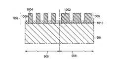
パッド本体202は、第1の研磨面204及び、第1の研磨面204とは反対側の第2の平坦面206を含む。パッド本体202は、複数の溝210またはチャネルを有する下部208を含む。複数の溝210またはチャネルは、パッド本体202の下部208の上で延びている。複数の溝210またはチャネルは、研磨パッド200の溝付き表面を形成する研磨面204内に配置されている。溝210は、任意の適切な形状であってよい。溝210は、円形であってよい。溝が円形であるある実施形態では、溝210は、互いに同心であってよい。
The
溝210は、ピッチPで間隔を空けて配置されている。ピッチPは、図2Bに最も明確に示されているとおり、隣接する溝間の、径方向の距離である。各溝間には、幅Wpを有する特徴部212または仕切りが存在する。特徴部212は、任意の適切な形状であってよい。特徴部212は、環状の特徴部であってよい。各溝210は壁214を含んでおり、壁214はベース部216で終端している。図2Bに示すとおり、ベース部216は、長方形のプロファイルを有していてよい。代わりに、ベース部216が、U字形のプロファイルを有していてもよい。各溝210は、深さDg及び幅Wgを有していてよい。壁214は概して垂直であってよく、ベース部216で終端していてよい。
The
一実施形態では、特徴部212の上表面222が、パッド本体202の下部208から突き出すように、特徴部212の高さ220は、各溝210のベース部216よりも高くなっている。特徴部212とベース部216との間に、溝210またはチャネルが形成されている。研磨中には、特徴部212の上表面222が基板と接触する研磨面204を形成している一方、溝210は、研磨流体を保持している。
In one embodiment, the
一実施形態では、特徴部212の幅Wpは、約250ミクロンと約2ミリメートルの間であってよい。溝210の幅Wgは、約250ミクロンと約2ミリメートルの間であってよい。特徴部212間のピッチ「P」は、約0.5ミリメートルと約5ミリメートルの間であってよい。特徴部212の幅Wp、溝210の幅Wg、及び/またはピッチ「P」は、様々な硬度のゾーンに合わせて、研磨パッド200の半径全体にわたって変化していてよい。
In one embodiment, the width Wp of the
パッド本体202は、複数の露出面を含んでいてよい。一実施形態では、複数の表面中の露出面のうちの2つのうちの少なくとも一部が有する、ゼータ電位といった表面特性は、異なっている。一実施形態では、各露出面内の諸領域は変更されて、異なるゼータ電位を有している。露出面は、ゼータ電位が上昇勾配を形成するようにして選択されてよい。一実施形態では、露出面は、第1の研磨用特徴部212の上表面222、壁214の表面224、及びベース部216の表面226から選択される。例えば、一実施例では、第1の研磨用特徴部212の上表面222の少なくとも一部は第1のゼータ電位を有する第1の材料を含み、壁214の表面224の少なくとも一部は第2のゼータ電位を有する材料を含み、溝210のベース部216の表面226の少なくとも一部は第3のゼータ電位を有する第3の材料を含む。別の実施形態では、少なくとも特徴部212の上表面222の一部及び壁214の表面224の一部は第1のゼータ電位を有し、溝210のベース部216の表面226の少なくとも一部は、第1のゼータ電位とは異なる第2のゼータ電位を有する第2の材料を含む。
The
図2Cを参照すると、パッド本体202は、複数の材料層2301〜2309(230と総称する)を含んでいてよい。種々の層のそれぞれを形成するため、ゼータ電位といった種々の表面特性を有する材料が使用されてよい。複数の材料層2301〜2309のうちの少なくとも2つの層は、それぞれ他の層の露出面とは異なるゼータ電位を有する露出面を有する。図2Cに示す研磨パッド200が、9つの層を含むものとして示されているのは例示のために過ぎず、ゼータ電位の所望の勾配を作成するために任意の数の材料層230が使用されてよいことは、理解されるべきである。
Referring to FIG. 2C, the
一実施形態では、パッド本体202の全体を通じて、ゼータ電位が傾斜を有している。ゼータ電位は、研磨面204から平坦面206に向けて、パッド本体202全体を通じて、ある材料特性勾配(240→250)で傾斜していてよい。一実施形態では、中性溶液を使って測定された、変化している材料特性勾配(240→250)のゼータ電位は、約−70mVと約+50mVの間の範囲内で変化している。一実施形態では、ゼータ電位の勾配は、研磨面204から平坦面206に向けて上昇している。例えば、一実施形態では、1つ以上の露出した第1の領域または表面、及び1つ以上の第2の領域または表面は、研磨面204から平坦面206に向けてゼータ電位が上昇する、ゼータ電位の勾配を形成するようにして配置されている。別の実施形態では、ゼータ電位の勾配は、平坦面206から研磨面204に向けて上昇している。例えば、一実施形態では、第1の研磨用特徴部212の上表面222は第1のゼータ電位を有する材料の第1の材料層2301を含み、壁214の表面224の少なくとも一部は第2のゼータ電位を有する第2の材料層(2302〜2308の任意の組み合わせ)を含み、溝210のベース部216の表面226は第3のゼータ電位を有する第3の材料層2308を含む。別の実施形態では、材料層2301〜2308は第1のゼータ電位を有し、材料層2309は第2のゼータ電位を有する。
In one embodiment, the zeta potential has a slope throughout the
図3Aは、本開示の別の実施形態による、領域によってゼータ電位が変化している表面を有する研磨パッド300の概略斜視図である。図3Bは、図3Aの研磨パッド300の一部の概略断面図である。研磨パッド300は、化学機械研磨によって基板を研磨するため、研磨ステーション100といった研磨ステーションにおいて使用されてよい。この研磨パッドは、研磨パッド300が、露出した領域または表面を有する複数の別個の特徴部を含んでいることを除き、研磨パッド200と同様である。一実施形態では、複数の領域または表面のうちの、露出した領域または表面のうちの少なくとも2つが有する、ゼータ電位といった表面特性は、異なっている。一実施形態では、CMPプロセス中に生成された研磨材粒子及び金属汚染物質といった研磨時の副生成物が、基板と研磨パッドとの間の研磨界面から取り除かれ、活性スラリが基板と研磨パッドとの間の界面に給送されるようにして、諸領域または諸表面のゼータ電位が調節されてよい。
FIG. 3A is a schematic perspective view of a
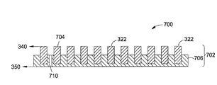
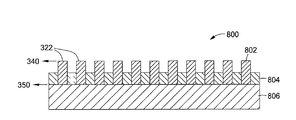
研磨パッド300は、複合材パッド本体302を含む。複合材パッド本体302は、第1の研磨面305及び、第1の研磨面305とは反対側の、第2の平坦面307を含む。この複合材パッド本体302は、1つ以上の第1の研磨用特徴部304と、1つ以上の第2の研磨用特徴部306とを含む。1つ以上の第1の研磨用特徴部304と1つ以上の第2の研磨用特徴部306のうちの少なくとも1つの、露出面のうちの少なくとも2つの一部は、様々なゼータ電位の表面を持つために、本明細書に記載するように変更されてよい。第1の研磨用特徴部304と第2の研磨用特徴部306は、境界で1つに接合されて複合材パッド本体302を形成している、不連続な複数の特徴部である。一実施形態では、第1の研磨用特徴部304は、約40ショアDスケール〜約90ショアDスケールの硬さを有する、硬性の特徴部であってよい。第2の研磨要素306は、約26ショアAスケールと約95ショアAスケールの間の硬さの値を有する、弾性の特徴部であってよい。
The
複合材パッド本体302を形成するための例示的な技法は、3D印刷、成形、鋳造、及び焼結を含む。複合材パッド本体302は複数の層を含んでいてよく、これらの複数の層のそれぞれは、3Dプリンタによって堆積される複合材パッド本体302の設計による、第2の研磨用特徴部306の領域及び/または第1の研磨用特徴部304の領域を含んでいてよい。複数の層は次いで、例えばUV光によって、または熱源によって硬化されて、固化し、目標の硬さに到達し得る。堆積及び硬化の後に、連結されているかまたは接合されており、ゼータ電位が様々である露出面を持つ、第1の研磨用特徴部304と第2の研磨用特徴部306とを含む、一体型の複合材パッド本体302が形成される。
Exemplary techniques for forming the
目標とする研磨プロセスを実現するため、第2の研磨用特徴部306用と第1の研磨用特徴部304用とで、別々の機械的特性を有する材料が選択されてよい。第2の研磨用特徴部306と第1の研磨用特徴部304の動的機械特性は、特徴部の形成プロセス中に使用される、種々の材料を選択すること、及び/または種々の硬化プロセスを選ぶことによって、実現され得る。一実施形態では、第2の研磨用特徴部306がより低い硬さの値とより低いヤング率の値を有していてよい一方、第1の研磨用特徴部304は、より高い硬さの値とより高いヤング率の値を有していてよい。一実施形態では、第2の研磨用特徴部306がより低いゼータ電位値を有していてよい一方、第1の研磨用特徴部304は、より高いゼータ電位値を有していてよい。別の実施形態では、第2の研磨用特徴部306がより低いゼータ電位値を有していてよい一方、第1の研磨用特徴部304は、より高いゼータ電位値を有していてよい。本明細書に記載のとおり、ゼータ電位といった表面特性は、研磨パッドの研磨面内または研磨面全体にわたって、各特徴部内で、及び/または、第2の研磨用特徴部306と第1の研磨用特徴部304の物理的なレイアウト、パターン、もしくは組み合わせによって、制御され得る。
In order to realize the target polishing process, materials having different mechanical properties may be selected for the
第1の研磨用特徴部304は、1つ以上のポリマー材料から形成されていてよい。第1の研磨用特徴部304は、本明細書に記載のとおり種々のゼータ電位を有する露出面を実現するために様々なゼータ電位調整剤と組み合わされた、単一のポリマー材料、または2つ以上のポリマーの混合物によって形成されていてよい。一実施形態では、第1の研磨用特徴部304は、1つ以上の熱可塑性ポリマーから形成されていてよい。第1の研磨用特徴部304は、ポリウレタン、ポリプロピレン、ポリスチレン、ポリアクリロニトリル、ポリメチルメタクリレート、ポリクロロトリフルオロエチレン、ポリテトラフルオロエチレン、ポリオキシメチレン、ポリカーボネート、ポリイミド、ポリエーテルエーテルケトン、ポリフェニレンスルファイド、ポリエーテルスルホン、アクリロニトリルブタジエンスチレン(ABS)、ポリエーテルイミド、ポリアミド、メラミン、ポリエステル、ポリスルホン、ポリビニルアセテート、フッ化炭化水素などといった熱可塑性ポリマー、並びに、そのアクリレート、コポリマー、グラフト鎖、及び混合物から形成されていてよい。別の実施形態では、本明細書に記載のとおり種々のゼータ電位を有する露出面を実現するため、第1の研磨用特徴部304を形成するのに使われる熱可塑性ポリマーは、様々なゼータ電位調整剤で変更されている。一実施形態では、第1の研磨用特徴部304は、アクリレートから形成されていてよい。例えば、第1の研磨用特徴部304は、ポリウレタンアクリレート、ポリエーテルアクリレート、またはポリエステルアクリレートであってよい。別の実施形態では、第1の研磨用特徴部304は、エポキシ、フェノール、アミン、ポリエステル、ウレタン、シリコンといった、1つ以上の熱硬化性ポリマー、並びにそのアクリレート、混合物、コポリマー、及びグラフト鎖を含んでいてよい。
The
一実施形態では、第1の研磨用特徴部304は、シミュレーションプラスチックの3D印刷材料で形成されていてよい。一実施形態では、研磨処理強化のため、第1の研磨要素304内に研磨材粒子が埋め込まれていてよい。研磨材粒子を含む材料は、セリア、アルミナ、シリカ、もしくはそれらの組み合わせなどの金属酸化物、ポリマー、金属間化合物、またはセラミックであってよい。
In one embodiment, the
第2の研磨用特徴部306は、1つ以上のポリマー材料から形成されていてよい。目標とする特性を実現するため、第2の研磨用特徴部306は、単一のポリマー材料、または2つ以上のポリマーの混合物から形成されていてよい。一実施形態では、第2の研磨用特徴部306は、1つ以上の熱可塑性ポリマーから形成されていてよい。例えば、第2の研磨用特徴部306は、ポリウレタン、ポリプロピレン、ポリスチレン、ポリアクリロニトリル、ポリメチルメタクリレート、ポリクロロトリフルオロエチレン、ポリテトラフルオロエチレン、ポリオキシメチレン、ポリカーボネート、ポリイミド、ポリエーテルエーテルケトン、ポリフェニレンスルファイド、ポリエーテルスルホン、アクリロニトリルブタジエンスチレン(ABS)、ポリエーテルイミド、ポリアミド、メラミン、ポリエステル、ポリスルホン、ポリビニルアセテート、フッ化炭化水素などといった熱可塑性ポリマー、並びに、そのアクリレート、コポリマー、グラフト鎖、及び混合物から形成されていてよい。別の実施形態では、本明細書に記載のように種々のゼータ電位を有する露出領域を実現するため、第2の研磨用特徴部306を形成するのに使われる熱可塑性ポリマーは、様々なゼータ電位調整剤で変更されている。一実施形態では、第2の研磨用特徴部306は、アクリレートから形成されていてよい。例えば、第2の研磨用特徴部306は、ポリウレタンアクリレート、ポリエーテルアクリレート、またはポリエステルアクリレートであってよい。別の実施形態では、第2の研磨用特徴部306は、熱可塑性エラストマから形成されていてよい。一実施形態では、第2の研磨用特徴部306は、ゴム様の3D印刷材料から形成されていてよい。
The
ある実施形態では、第1の研磨用特徴部304が、概して第2の研磨用特徴部306よりも硬く、より剛性が高い一方で、第2の研磨用特徴部306は、第1の研磨用特徴部304よりも柔らかく、より可撓性が高い。第1の研磨用特徴部304及び第2の研磨用特徴部306の材料とパターンは、領域によって様々なゼータ電位を有する研磨パッド300の「調節された(tuned)」バルク材料が実現するようにして、選択されてよい。この「調節された」バルク材料で形成され、様々なゼータ電位を有する研磨パッド300は、研磨結果の改善(例えば欠陥の減少)、製造コストの削減、パッド寿命の延長といった、様々な利点を有している。一実施形態では、「調節された」バルク材料または研磨パッドは、全体として約65ショアAと約75ショアDの間の硬度を有していてよい。研磨パッドの引張強さは、5MPaと約75MPaの間であってよい。研磨パッド300は、約5%から約350%までの破断伸びを有していてよい。研磨パッドは、約10mPaを超えるせん断強さを有していてよい。研磨パッド300は、約5MPaと約2000MPaの間の貯蔵弾性率を有していてよい。研磨パッドは、30°Cにおける貯蔵弾性率E’をE’30、90°Cにおける貯蔵弾性率E’をE’90としたときに、E’30/E’90の貯蔵弾性率比が約6と約30の間の範囲になるように、25°C〜90°Cの温度範囲にわたって、安定した貯蔵弾性率を有していてよい。
In one embodiment, the
一実施形態では、第1の研磨用特徴部304の材料及び第2の研磨用特徴部306の材料は、研磨スラリからの攻撃に対して化学的耐性を有する。別の実施形態では、第1の研磨用特徴部304の材料及び第2の研磨用特徴部306の材料は、親水性である。
In one embodiment, the material of the
複合材パッド本体302は、複合材パッド本体302の第2の研磨用特徴部306の下部308の上方で延びている、複数の溝310またはチャネルを含む。複数の溝310またはチャネルは、研磨パッド300の研磨面305内に配置されている。溝310は、任意の適切な形状であってよい。溝310は、円形であってよい。溝が円形をしているある実施形態では、溝310は、互いに同心であってよい。
The
溝310は、ピッチPで間隔を空けて配置されている。ピッチPは、図3Bに最も明確に示されているとおり、隣接する溝間の、径方向の距離である。各溝間には、幅Wpを有する第1の研磨用特徴部304または仕切りが存在する。第1の研磨用特徴部304は、任意の適切な形状であってよい。第1の研磨用特徴部304は、環状の特徴部であってよい。各溝310は壁314を含んでおり、壁314はベース部316で終端している。図3Bに示すとおり、ベース部316は、長方形のプロファイルを有していてよい。代わりに、ベース部316が、U字形のプロファイルを有していてもよい。各溝310は、深さDg及び幅Wgを有していてよい。壁314は概して垂直であってよく、ベース部316で終端していてよい。
The
一実施形態では、第1の研磨用特徴部304及び第2の研磨用特徴部306は、円形の複合材パッド本体302を形成するように交互に配置された、交互同心リングであってよい。一実施形態では、第1の研磨用特徴部304の高さは、第2の研磨用特徴部306の高さよりも高く、そのため第1の研磨用特徴部304の上表面322は、第2の研磨用特徴部306から突き出ている。第1の研磨用特徴部304と第2の研磨用特徴部306との間に、溝310またはチャネルが形成されている。研磨中、第1の研磨用特徴部304の上表面322が基板と接触する研磨面305を形成している一方、溝310は、研磨流体を保持している。一実施形態では、複合材パッド本体302の頂面上に溝310及び/またはチャネルが形成されるように、第1の研磨用特徴部304は、複合材パッド本体302に平行な平面に対して直角方向に、第2の研磨用特徴部306よりも厚くなっている。
In one embodiment, the
一実施形態では、第1の研磨用特徴部304の幅Wpは、約250ミクロンと約2ミリメートルの間であってよい。第1の研磨要素304間のピッチ「P」は、約0.5ミリメートルと約5ミリメートルの間であってよい。各第1の研磨要素304は、約250ミクロンと約2ミリメートルの間の範囲内の幅を有していてよい。幅Wp及び/またはピッチ「P」は、様々な硬さのゾーンに合わせて、研磨パッド300の半径全体にわたって変化していてよい。
In one embodiment, the width Wp of the
複合材パッド本体302は、複数の露出面を含んでいてよい。一実施形態では、複数の表面中の露出面のうちの2つのうちの少なくとも一部が持つ、ゼータ電位といった表面特性は、異なっている。露出面は、ゼータ電位が上昇勾配を形成するようにして、選択されていてよい。一実施形態では、露出面は、第1の研磨用特徴部304の上表面322、壁314の表面324、及びベース部316の表面326から選択される。例えば、一実施例では、第1の研磨用特徴部304の上表面322の少なくとも一部は第1のゼータ電位を有する第1の材料を含み、壁314の表面324の少なくとも一部は第2のゼータ電位を有する材料を含み、溝310のベース部316の表面326の少なくとも一部は第3のゼータ電位を有する第3の材料を含む。別の実施形態では、少なくとも第1の研磨用特徴部304の上表面322の一部及び第1の研磨用特徴部304の壁314の表面324の一部は第1のゼータ電位を有し、溝210のベース部316の表面326の少なくとも一部は、第1のゼータ電位とは異なる第2のゼータ電位を有する第2の材料を含む。
The
一実施形態では、複合材パッド本体302は、図2Cに示すように複数の材料層を含んでいてよい。種々の層のそれぞれを形成するため、ゼータ電位といった種々の表面特性を有する材料が使用されてよい。複数の層のうちの少なくとも2つの層は、それぞれ他の層の露出面とは異なるゼータ電位を有する露出面を有する。
In one embodiment, the
一実施形態では、複合材パッド本体302の全体を通じて、ゼータ電位が傾斜を有している。ゼータ電位は、研磨面305から平坦面307に向けて、複合材パッド本体302全体を通じて、ある材料特性勾配(340→350)で傾斜していてよい。一実施形態では、ゼータ電位の勾配は、研磨面305から平坦面307に向かって上昇している。別の実施形態では、ゼータ電位の勾配は、平坦面305から研磨面307に向かって上昇している。例えば、一実施例では、第1の研磨用特徴部304の上表面322は第1のゼータ電位を有する材料の第1の層を含み、壁314の表面324の少なくとも一部は第2のゼータ電位を有する材料の第2の層を含み、溝310のベース部316の表面326は第3のゼータ電位を有する材料の第3の層を含む。
In one embodiment, the zeta potential has a slope throughout the
図3Cは、本開示の一実施形態による、領域によってゼータ電位が変化している表面を有する研磨パッド300cの概略部分上面図である。研磨パッド300cは、研磨パッド300cが互いに嵌合している第1の研磨用特徴部304cと第2の研磨用特徴部306cを含んでいることを除き、図3Aの研磨パッド300と同様である。第1の研磨用特徴部304c及び第2の研磨用特徴部306cは、複数の同心リングを形成していてよい。一実施形態では、第1の研磨用特徴部304cは、突き出た垂直リッジ360を含んでいてよく、第2の研磨用特徴部306cは、垂直リッジ360を受容するための垂直凹部370を含んでいてよい。代わりに、第2の研磨用特徴部306cが突き出たリッジを含んでいてよい一方で、第1の研磨用特徴部304cが凹部を含んでいてもよい。研磨パッド300cは、第2の研磨用特徴部306cが第1の研磨用特徴部304cと嵌合していることによって、CMPプロセス中及び/または材料を扱っている間に発生し得るせん断力の印加に対する機械的強さが強化されている。第1の研磨要素304c及び第2の研磨要素306cは、それぞれ、ゼータ電位が変化している領域を有していてよい。
FIG. 3C is a schematic partial top view of the
図3Dは、本開示の実施形態による、領域によってゼータ電位が変化している表面を有する研磨パッド300dの概略斜視断面図である。研磨パッド300dは、第2の研磨用特徴部306dといったベース材料層から延びる、複数の第1の研磨用特徴部304dを含む。第1の研磨用特徴部304dの上表面372は、研磨中に基板に接触する研磨面を形成している。第1の研磨用特徴部304dと第2の研磨用特徴部306dとは、異なる材料特性及び構造特性を有する。例えば、第1の研磨用特徴部304dが、研磨パッド300の第1の研磨用特徴部304用の材料といった、第1のゼータ電位を有する材料から形成されていてよい一方、第2の研磨用特徴部306dは、第2のゼータ電位を有する材料から形成されていてよい。さらに、第1の研磨用特徴部304dが、研磨パッド300の硬性の特徴部用の材料といった硬い材料で形成されていてよい一方、第2の研磨用特徴部306dは、研磨パッド300の第2の研磨用特徴部用の材料といった、軟らかい即ち低貯蔵弾性率E’の材料で形成されていてよい。研磨パッド300dは、研磨パッド300と同様に、3D印刷によって形成されていてよい。
FIG. 3D is a schematic perspective sectional view of the polishing pad 300d having a surface in which the zeta potential changes depending on the region according to the embodiment of the present disclosure. The polishing pad 300d includes a plurality of first
一実施形態では、第1の研磨用特徴部304dは、ほぼ同じサイズであってよい。代わりに、研磨パッド300d全体にわたる、ゼータ電位の変化、貯蔵弾性率E’の変化、及び/または損失弾性率E’’の変化といった機械的特性及び表面特性の変化を生じさせるために、第1の研磨用特徴部304dのサイズは様々であってよい。一実施形態では、第1の研磨用特徴部304dは、研磨パッド300d全体にわたって均一に分布していてよい。代わりに、第1の研磨用特徴部304dは、研磨パッド300dの目標の特性を実現するために、不均一なパターンで配置されていてもよい。
In one embodiment, the
図3Dでは、第1の研磨用特徴部304dは、第2の研磨用特徴部306dから突き出た円柱として示されている。代わりに、第1の研磨用特徴部304dは、例えば楕円形、正方形、長方形、三角形、多角形、または不定形の断面を有する柱状体などの、任意の適切な形状であってよい。一実施形態では、第1の研磨用特徴部304dは、高機能研磨パッドの硬さ、機械的強さ、ゼータ電位、または他の所望の特性を調節するため、種々の断面形状のものであってよい。
In FIG. 3D, the
図3Eは、本開示の一実施形態による、領域によってゼータ電位が変化している表面を有する研磨パッド300eの概略部分断面図である。研磨パッド300eは、研磨パッド300eが互いに嵌合している第1の研磨用特徴部304eと第2の研磨用特徴部306eを含んでいることを除き、図3A〜図3Dの研磨パッド300、300c、または300dと同様である。第1の研磨用特徴部304eと第2の研磨用特徴部306eは、複合材パッド本体202の一部を形成する、複数の同心リング及び/または別個の要素を含んでいてよい。一実施形態では、第1の研磨用特徴部304eは、突き出た側壁374を含んでいてよく、一方で第2の研磨用特徴部306eは、第1の研磨用特徴部304eを受容するための凹型の側壁375を含んでいてよい。代わりに、第2の研磨用特徴部306eが突き出た側壁を含んでおり、一方で第1の研磨用特徴部304eが凹んだ側壁を含んでいてもよい。第2の研磨用特徴部306eと第1の研磨用特徴部304eが突き出た側壁によって嵌合していることで、研磨パッド300eは、引張強さ、圧縮強さ、及び/またはせん断強さが増大する。加えて、側壁が嵌合していることによって、研磨パッド300eが引っ張られてばらばらになることが防止される。
FIG. 3E is a schematic partial cross-sectional view of the
一実施形態では、第1の研磨用特徴部304eと第2の研磨用特徴部306eとの境界は、第1の研磨用特徴部304eを形成するのに使われている第1の組成物から第2の研磨用特徴部306eを形成するのに使われている第2の組成物への遷移または組成勾配といった、少なくとも1つの組成物の材料から別の組成物の材料への凝集した(cohesive)遷移を含む。複合材パッド本体302の部分を形成するのに使用された組成物からこうして形成された材料の凝集性は、本明細書に記載の付加製造プロセスの直接的な結果であり、これによって、層ごと付加的に形成された構造内の1つ以上の化学的組成をミクロンのスケールで制御し、密に混合することが可能になる。
In one embodiment, the boundary between the
図3Fは、本開示の一実施形態による、領域によってゼータ電位が変化している表面を有する研磨パッド300fの概略部分断面図である。図3Fは、本開示の一実施形態による研磨パッドの概略的な部分断面図である。研磨パッド300fは、研磨パッド300fが別様に構成された嵌合用特徴部を含んでいることを除き、図3Eの研磨パッド300eと同様である。研磨パッド300fは、第1の研磨用特徴部304f及び第2の研磨用特徴部306fを含んでいてよい。第1の研磨用特徴部304fと第2の研磨用特徴部306fは、複数の同心リング及び/または別個の要素を含んでいてよい。一実施形態では、第1の研磨用特徴部304fが水平リッジ376を含んでいてよい一方、第2の研磨用特徴部306fは、第1の研磨用特徴部304fの水平リッジ376を受容するための水平凹部377を含んでいてよい。代わりに、第2の研磨用特徴部306fが水平リッジを含んでいてよい一方で、第1の研磨用特徴部304fが水平凹部を含んでいてもよい。一実施形態では、図3Cの嵌合用特徴部といった垂直の嵌合用特徴部と、図3E及び図3Fの嵌合用特徴部といった水平の嵌合用特徴部とが組み合わされて、研磨パッドを形成してよい。
FIG. 3F is a schematic partial cross-sectional view of a
図3G〜図3Lは、本開示の一実施形態による、領域によってゼータ電位が変化している表面を有する研磨パッド設計の上面図である。図3G〜図3Lの各々は、基板と接触して基板を研磨するための、第1の研磨用特徴部304g〜304lをそれぞれ表す白色領域(白色ピクセルの領域)と、第2の研磨用特徴部306g〜306lを表す黒色領域(黒色ピクセルの領域)とを有する、ピクセルチャートを含む。第1の研磨用特徴部304g〜304lは、本明細書に記載の第1の研磨用特徴部304と同様であってよい。第2の研磨用特徴部306g−306l は、研磨パッドの第2の研磨用特徴部306と同様であってよい。同じく本明細書で検討されているように、白色領域は概して黒色領域の上方に突き出ており、それによって白色領域間の黒色領域内にチャネルが形成されている。研磨スラリは、研磨中に、チャネルを通って流れてよく、かつ、チャネル内に保持されうる。図3G〜図3Lに示す研磨パッドは、付加製造プロセスを用いて複数の材料層を堆積させることによって形成されていてよい。複数の層の各々は、第1の研磨用特徴部304g〜304f、及び第2の研磨用特徴部306g〜306fを形成する、2つ以上の材料を含んでいてよい。一実施形態では、第1の研磨用特徴部304g〜304fは、研磨パッドの頂面上に溝及び/またはチャネルが形成されるように、材料の複数の層に平行な平面に対して直角の方向に、第2の研磨用特徴部306g〜306fよりも厚くてよい。
3G to 3L are top views of a polishing pad design having a surface in which the zeta potential changes depending on the region according to one embodiment of the present disclosure. Each of FIGS. 3G to 3L has a white region (white pixel region) representing the first
図3Gは、同心円の研磨用特徴部である第1の研磨用特徴部304gを有する研磨パッド設計300gの、概略的なピクセルチャートである。第1の研磨用特徴部304gは、同一幅の同心円であってよい。一実施形態では、第1の研磨用特徴部304gのピッチが半径方向に沿って一定になるように、第2の研磨用特徴部306gもまた、同一の幅を有していてよい。研磨中、第1の研磨用特徴部304g間のチャネルが、研磨スラリを保持し、研磨パッドの中心軸(すなわち同心円の中心)を中心とした研磨パッドの回転によって生成される遠心力による、研磨スラリの急速な損失を防止する。
FIG. 3G is a schematic pixel chart of a
図3Hは、同心円に配置された複数の区分けされた第1の研磨用特徴部304hを有する研磨パッド設計300hの、概略的なピクセルチャートである。一実施形態では、区分けされた第1の研磨用特徴部304hは、ほぼ同一の長さを有していてよい。区分けされた第1の研磨用特徴部304hは、複数の同心円を形成していてよい。各円において、区分けされた第1の研磨要素304hは、各同心円内に均等に分布していてよい。一実施形態では、区分けされた第1の研磨用特徴部304hは、半径方向に同一の幅を有していてよい。ある実施形態では、区分けされた第1の研磨用特徴部304hはそれぞれ、同心円の半径に関わりなく、ほぼ同一の長さを有する(例えば、研磨パッドの中央領域を除いて弧長が等しい)。一実施形態では、第2の研磨用特徴部306hは、複数の同心円の間に配置されており、同心円のピッチが一定になるように、同一の幅を有している。一実施形態では、研磨パッドの中心軸を中心とした研磨パッドの回転によって生成される遠心力の影響によって研磨スラリが研磨パッドから直接流出することを防止するために、区分けされた第1の研磨用特徴部304h間の間隙は、円ごとに互い違いになっていてよい。
FIG. 3H is a schematic pixel chart of a
図3Iは、第2の研磨用特徴部306iの上一面に配置された、螺旋状の第1の研磨用特徴部304iを有する、研磨パッド設計300iの概略的なピクセルチャートである。図3Iでは、研磨パッド設計300iは、研磨パッドの中心から研磨パッドのエッジへと延びる、4つの螺旋状の第1の研磨用特徴部304iを有する。4つの螺旋状の研磨用特徴部が示されているが、より少ないかまたはより多い数の螺旋状の第1の研磨用特徴部304i が、同様の態様で配置されていてもよい。螺旋状の第1の研磨要素304iは、螺旋状のチャネルを画定する。一実施形態では、螺旋状の第1の研磨用特徴部304iの各々は、一定の幅を有する。一実施形態では、螺旋状のチャネルもまた一定の幅を有する。研磨中、研磨パッドは、螺旋状のチャネル内に研磨スラリを保持するために、螺旋状の第1の研磨用特徴部304iの方向とは反対の方向に、中心軸を中心に回転してよい。例えば図3Iでは、螺旋状の第1の研磨用特徴部304i及び螺旋状のチャネルは、反時計回り方向に形成されており、したがって研磨パッドは研磨中、時計回りに回転して、螺旋状のチャネル内及び研磨パッド上の研磨スラリを保持してよい。ある実施形態では、螺旋状のチャネルの各々は、研磨パッドの中心から研磨パッドのエッジまで連続している。この連続した螺旋状のチャネルは、研磨スラリが、研磨屑があればそれらと共に、研磨パッドの中心から研磨パッドのエッジへと流れることを可能にする。一実施形態では、螺旋状の第1の研磨用特徴部304iと同じ方向に(例えば図3Iでは反時計回りに)研磨パッドを回転させることによって、研磨パッドが洗浄されてよい。
FIG. 3I is a schematic pixel chart of a
図3Jは、第2の研磨用特徴部306j上に螺旋状のパターンで配置された、区分けされた研磨用特徴部である第1の研磨用特徴部304jを有する、研磨パッド設計300jの概略的なピクセルチャートである。図3Jに示す研磨パッドは、第1の研磨用特徴部304jが区分けされている点と第1の研磨用特徴部304jの径方向のピッチが変化している点を除き、図3Iの研磨パッドと同様である。一実施形態では、第1の研磨用特徴部304jの径方向ピッチは、研磨パッドの中心から研磨パッドのエッジ領域にかけて減少する。
FIG. 3J is a schematic diagram of a
図3Kは、第2の研磨用特徴部306k内に形成された、複数の別個の第1の研磨用特徴部304kを有する、研磨パッド設計300kの概略的なピクセルチャートである。一実施形態では、複数の第1の研磨用特徴部304kのそれぞれは、図3Dに示す構成と同様の、円柱ポストのタイプの構造であってよい。一実施形態では、複数の第1の研磨用特徴部304kは、研磨面の平面内で同じ寸法を有していてよい。一実施形態では、複数の第1の研磨要素304kは、同心円で配置されていてよい。一実施形態では、複数の第1の研磨用特徴部304kは、研磨面の平面に対する規則的な2Dのパターンで配置されていてよい。
FIG. 3K is a schematic pixel chart of a
図3Lは、第2の研磨用特徴部306fの上一面に形成された、複数の別個の複数の第1の研磨用特徴部304fを有する、研磨パッド設計300fの概略的なピクセルチャートである。図3Lの研磨パッドは、図3Lの第1の研磨用特徴部304fのあるものが接続されて1つ以上の閉じた円を形成していてよいことを除いて、図3Kの研磨パッドと同様である。1つ以上の閉じた円は、研磨中に研磨スラリを保持するための、1つ以上の堰き止め部を作成してよい。
FIG. 3L is a schematic pixel chart of a
図3Aから図3Lの設計における第1の研磨用特徴部304a〜304fは、同一の材料または同一の組成物の材料から形成されていてよい。代わりに、図3Aから図3Lの設計における第1の研磨用特徴部304a〜304fの材料組成及び/または材料特性は、研磨用特徴部ごとに変化していてもよい。材料組成及び/または材料特性が個別化されることで、研磨パッドを特定のニーズ向けにカスタマイズすることが可能になる。 The first polishing feature portions 304a to 304f in the design of FIGS. 3A to 3L may be formed of the same material or the same composition material. Alternatively, the material composition and / or material properties of the first polishing features 304a-304f in the design of FIGS. 3A to 3L may vary from polishing feature to polishing feature. Individualized material composition and / or material properties allow the polishing pad to be customized for specific needs.
図4Aは、本開示の1つ以上の実施形態による付加製造システムを用いて、領域によってゼータ電位が変化している表面を有する研磨パッドを形成するのに使用され得る、付加製造システム450の概略断面図である。付加製造処理は、限定しないが、ポリジェット堆積処理、インクジェット印刷処理、熱溶解積層処理、バインダージェッティング処理、粉末床溶融結合処理、選択的レーザ焼結処理、ステレオリソグラフィ処理、液槽光重合デジタルライトプロセシング、シート積層処理、指向性エネルギー堆積処理、または他の同様の3D堆積処理(例えば3D印刷処理)といった、処理を含み得る。3D印刷といった付加製造プロセスは、領域によってゼータ電位が変化している研磨パッドの形成において、特に有用であることが見出されてきた。
FIG. 4A outlines an
付加製造システム450は、一般的に、前駆体給送セクション453、前駆体形成セクション454、及び堆積セクション455を含む。堆積セクション455は、一般的に付加製造デバイスを含む。付加製造デバイスは以降、印刷ステーション400と呼ばれ、研磨パッド200、300〜300lの形成に使用される。処理中、研磨パッド200、300〜300lは、印刷ステーション400内の支持体402上で印刷されてよい。ある実施形態では、研磨パッド200、300〜300lは、図4Aに示すプリンタ406A及びプリンタ406Bといった1つ以上の液滴噴射プリンタ406を使用して、層ごとに、CAD(コンピュータ支援設計)プログラムから形成される。プリンタ406A、406Bと支持体402とは、印刷処理中に、互いに対して移動し得る。
The
液滴噴射プリンタ406は、液体前駆体を分注するための1つ以上のノズル(例えばノズル409〜412)を有する、1つ以上のプリントヘッド408を含み得る。図4Aの実施形態では、プリンタ406Aは、ノズル409を有するプリントヘッド408Aと、ノズル410を有するプリントヘッド408Bとを含む。ノズル409が、第1のゼータ電位を有するポリマー材料といった第1のポリマー材料を形成する第1の液体前駆体組成物を分注するように構成されていてよい一方、ノズル410は、第2のゼータ電位を有する第2のポリマー材料を形成する第2の液体前駆体を分注するために使用されてよい。液体前駆体組成物は、様々なゼータ電位の領域を有する研磨パッドを形成するため、選択された箇所または領域に分注されてよい。これらの選択された箇所は、合わせて、CAD適合ファイルとして保存され得る目標の印刷パターンを形成しており、この目標の印刷パターンは後に、液滴噴射プリンタ406のノズルからの液滴の給送を制御する電子コントローラ405によって読み込まれる。
The droplet injection printer 406 may include one or more printheads 408 having one or more nozzles (eg, nozzles 409-412) for dispensing the liquid precursor. In the embodiment of FIG. 4A, the
電子コントローラ405は、概して、印刷ステーション400を含む付加製造システム450内の構成要素の制御と自動化を促進するために使用される。電子コントローラ405は、例えば、コンピュータ、プログラム可能論理コントローラ、または組込型コントローラであり得る。コントローラ405は、典型的には、中央処理装置(CPU)、メモリ(例えば、コンピュータ可読媒体)、及び入出力(I/O)用補助回路(図示せず)を含む。CPUは、様々なシステム機能、基板の移動、チャンバ処理、及び制御支援ハードウエア(例えばセンサ、モータ、ヒータなど)を制御するために工業環境で使用される任意の形態のコンピュータプロセッサのうちの1つであってよく、システム内で実施される処理をモニタしてよい。メモリまたはコンピュータ可読媒体は、CPUに接続されており、ランダムアクセスメモリ(RAM)、フラッシュメモリ、読み取り専用メモリ(ROM)、フロッピーディスク、ハードディスク、または任意の他の形態のローカルもしくは遠隔のデジタルストレージなど、容易に利用可能な非揮発性メモリのうちの1つ以上であってよい。メモリ内には、CPUに命令するためのソフトウェア命令及びデータをコード化して記憶させることができる。従来の方法でプロセッサをサポートするように、補助回路もまた、CPUに接続される。補助回路は、キャッシュ、電源、クロック回路、入出力回路、サブシステムなどを含んでいてよい。電子コントローラ405が読むことができるプログラム(またはコンピュータ命令)が、どのタスクが付加製造システム450の構成要素によって実行可能かを決定する。一実施形態では、プログラムは、電子コントローラ405で読み取り可能なソフトウェアであり、液滴噴射プリンタ406から給送される液滴の、給送と位置決めのモニタリング、実行、及び制御に関するタスクを実施するコードを含む。プログラムは、電子コントローラ405内で実行中の様々な処理タスク及び様々なシーケンスと並行して、印刷ステーション400内の構成要素の移動、支持、及び/または位置決めに関するタスクもまた、含んでいてよい。
The
研磨パッド200、300〜300lは、3D印刷の後、付加製造システム450の堆積セクション455内に配置された硬化デバイス420を使用して固化されてよい。硬化デバイス420によって実施される硬化処理は、印刷された研磨パッドを硬化温度まで加熱するか、またはパッドを1つ以上の形態の電磁放射に曝露することによって、実施されてよい。一実施例では、硬化プロセスは、印刷された研磨パッドを硬化デバイス420内の紫外光源によって生成された紫外放射421に曝露することによって、実施されてよい。
The polishing
付加製造プロセスは、種々の材料及び/または種々の組成物の材料から形成された別個の特徴部を有する研磨パッドを作製するための、便利で、高度に制御可能なプロセスを提供する。一実施形態では、付加製造プロセスを用いて、第1のゼータ電位を有する特徴部、及び/または第2のゼータ電位を有する特徴部が形成されてよい。例えば、研磨パッドの第1のゼータ電位を有する特徴部は、プリンタ406Bのノズル412から分注されたポリウレタンのセグメントを含有する第1の組成物から形成されていてよく、研磨パッドの第2のゼータ電位を有する特徴部は、プリンタ406Aのノズル410から分注された、第2の組成物の液滴から形成されてよい。さらに、第1の組成物の液滴は、研磨パッドの軟性の即ち低貯蔵弾性率E’の特徴部を形成するのに使用されてよく、第2の組成物の液滴は、研磨パッドの硬性の即ち高貯蔵弾性率の特徴部を形成するのに使用されてよい。
The additive manufacturing process provides a convenient and highly controllable process for making polishing pads with distinct features formed from different materials and / or materials of different compositions. In one embodiment, an additional manufacturing process may be used to form a feature with a first zeta potential and / or a feature with a second zeta potential. For example, the feature portion of the polishing pad having the first zeta potential may be formed from a first composition containing a segment of polyurethane dispensed from
別の実施形態では、第1の研磨用特徴部304及び/または第2の研磨用特徴部306は、それぞれ2つ以上の組成物の混合物から形成されていてよい。一実施例では、第1の組成物は、プリントヘッド408Aといった第1のプリントヘッドによって、液滴の形態で分注されてよく、第2の組成物は、プリンタ406Aのプリントヘッド408Bといった第2のプリントヘッドによって、液滴の形態で分注されてよい。第1の研磨用特徴部304を複数のプリントヘッドから給送された液滴の混合物で形成することは、典型的には、第1の研磨要素304に相当する複数のピクセルを、電子コントローラ405内に存在する堆積マップ内の所定のピクセルに合わせて位置合わせすることを含む。堆積マップは、概して、各組成物の様々な液滴が表面(例えばX−Y表面)にわたって配置される位置を表しており、これらの液滴は、堆積した層の積層(例えば、Z方向に積まれた層)の中で層を形成する。次に、プリントヘッド408Aは、第1の研磨用特徴部304が形成されるべき場所に相当するピクセルに合わせて位置合わせし、それから所定のピクセル上に液滴を分注してよい。こうして、第1の液滴組成物の液滴を堆積させることによって形成される第1の組成物の材料と、第2の液滴組成物の液滴を堆積させることによって形成される第2の組成物の材料を含む第2の材料とから、研磨パッドが形成されてよい。
In another embodiment, the
図4Bは、研磨パッド製造プロセス中の印刷ステーション400と研磨パッド300の、一部の概略近接断面図である。図4Bに示す一実施例で示されている印刷ステーション400は、研磨パッド300の一部を層ごとの堆積プロセスによって順次形成するのに使用される、2つのプリンタ406A及び406Bを含む。図4Bに示す研磨パッド300の一部は、例えば、最終的に形成される研磨パッド300の中の第1の研磨用特徴部304または第2の研磨用特徴部306のどちらかの一部を含んでいてよい。処理中、プリンタ406A及び406Bは、支持体402の第1の表面に対して、また続いて層ごとのプロセスによって支持体402上に堆積した成長中の研磨パッドの表面に対して、それぞれ液滴「A」または「B」を給送するように構成されている。図4Bに示すとおり、支持体402上に形成されている第1の層446の上に、第2の層448が堆積している。一実施形態では、第2の層448は、パッド製造プロセス内でプリンタ406A及び406Bの下流に配置された硬化装置420によって処理されている第1の層446の上に、形成される。
FIG. 4B is a schematic close-up view of a portion of the
ある実施形態で、プリンタ406A及び406Bのうちの1つ以上が先立って形成された第1の層446の表面446A上に液滴「A」及び/または「B」を堆積している間に、同時に、第2の層448の一部が硬化装置420によって処理されてよいことは、留意されるだろう。このケースでは、現在形成中の層は、硬化ゾーン449Aのそれぞれの側に配置された処理済み部分448A及び未処理部分448Bを含み得る。未処理部分448Bは、概して、分注された液滴443及び447といった、分注された液滴の列を含んでいる。これらの分注された液滴は、それぞれプリンタ406B及び406Aを使用して、先行して形成された第1の層446の表面446A上に堆積したものである。
In certain embodiments, while one or more of the
図4Cは、図4Bに示すように、先立って形成された第1の層446の表面446A上に配置された、分注された液滴443の近接断面図である。分注された液滴443中の材料の特性に基づいて、また表面446Aの表面エネルギーのせいで、分注された液滴は、表面張力によって本来分注された液滴(例えば液滴「A」または「B」)のサイズよりも大きい量で、表面にわたって広がる。分注された液滴が広がる量は、液滴が表面446A上に堆積した瞬間からの時間に応じて変化するであろう。しかし、非常に短い時間(例えば<1秒)の経過後に、液滴の広がりは平衡サイズに到達し、接触角αを有するであろう。分注された液滴が表面にわたって広がることによって、成長中の研磨パッドの表面上に液滴が置かれる解像度が、したがって最終的な研磨パッドの様々な領域内に見られる特徴部及び組成物の解像度が、影響される。
FIG. 4C is a close cross-sectional view of the dispensed
ある実施形態では、液滴が基板表面で未硬化の平衡サイズに広がる機会を持つ前に、液滴「A」及び「B」を分注するのと同時にこれらの液滴を曝露して、各液滴を所望のサイズで硬化、即ち所望のサイズに「固定」することが望ましい。この場合、分注された各液滴の解像度を制御するために、硬化装置420によって分注された液滴及び液滴が置かれた表面に対して供給されるエネルギー、並びに液滴の材料組成が調整される。したがって、3D印刷プロセス中に制御または調節を行うべき1つのパラメータは、分注された液滴の、液滴が置かれた表面に対する表面張力の制御である。また、以下でさらに検討されるように、ある実施形態では、硬化プロセスの動態を制御し、酸素阻害を防止し、及び/または液滴が堆積された表面上における液滴の接触角を制御するため、液滴の調合物に対して1つ以上の開始剤(例えば光開始剤)を添加することが望ましい。
In one embodiment, the droplets "A" and "B" are dispensed and at the same time exposed to each of the droplets before they have the opportunity to spread to an uncured equilibrium size on the substrate surface. It is desirable to cure the droplets to the desired size, i.e. "fix" to the desired size. In this case, in order to control the resolution of each droplet dispensed, the droplets dispensed by the
分注された各液滴の表面特性及び寸法を印刷処理中に「固定」するため、分注された各液滴を部分的にのみ硬化するのが望ましいことが分かっている。液滴を所望のサイズで「固定」する能力は、液滴の材料組成に対して1つ以上の光開始剤を所望の量で添加することと、印刷プロセス中に十分な量のエネルギーを硬化デバイス420から送ることによって、実現することができる。ある実施形態では、液滴分注及び付加層形成プロセス中に、平方センチ当たり約1ミリジュール(mJ/cm2)と100mJ/cm2の間、例えば約10〜15mJ/cm2の紫外線(UV)を液滴に送ることが可能な、硬化デバイス420を使用することが望ましい。UV放射は、水銀マイクロ波アークランプ、パルス式キセノンフラッシュランプ、高効率UV発光ダイオードアレイ、及びUVレーザといった、任意のUV源によって提供されてよい。UV放射は、約170nmと約400nmの間の波長を有していてよい。
It has been found desirable to only partially cure each dispensed droplet in order to "fix" the surface properties and dimensions of each dispensed droplet during the printing process. The ability to "fix" the droplets to the desired size is the addition of one or more photoinitiators to the material composition of the droplets in the desired amount and curing sufficient amount of energy during the printing process. This can be achieved by sending from
ある実施形態では、分注された液滴「A」及び「B」のサイズは、50〜約70ミクロンといったように、約10〜約100ミクロンであってよい。液滴が上一面に及び上に分注された基板またはポリマー層の表面エネルギー(dyne)に応じて、未硬化の液滴は、表面上で及び表面にわたって、約10ミクロンと約500ミクロンの間、例えば約50ミクロンと約200ミクロンの間の固定された液滴のサイズ443Aに広がってよい。こうした液滴の高さは、ここでもまた、表面エネルギー、濡れ、及び/または、流動剤、増粘剤、及び界面活性剤といった他の添加剤を含み得る樹脂の組成、といった要素に応じて、約5ミクロンから約100ミクロンまでであってよい。上記の添加材の1つの供給元は、ドイツ国ゲーレッツリートのBYK−ガードナーGmbHである。 In certain embodiments, the size of the dispensed droplets "A" and "B" may be about 10 to about 100 microns, such as 50 to about 70 microns. Depending on the surface energy (dyne) of the substrate or polymer layer in which the droplets are dispensed over and over, the uncured droplets are between about 10 microns and about 500 microns on and over the surface. For example, it may spread to a fixed droplet size of 443A between about 50 microns and about 200 microns. The height of these droplets also depends on factors such as surface energy, wetting, and / or the composition of the resin, which may contain other additives such as fluids, thickeners, and surfactants. It can be from about 5 microns to about 100 microns. One source of the above additives is BYK-Gardner GmbH of Geretsried, Germany.
一般的に、約1秒未満以内、例えば約0.5秒未満以内の時間で「固定される」のを可能にするために、光開始剤、液滴の組成中の光開始剤の量、及び硬化デバイス420が供給するエネルギーの量を選択することが望ましい。この短い時間枠の中で液滴を「固定」しようとするためには、ノズル及び研磨パッドの表面446Aを硬化デバイス420から送られた紫外放射421に曝露する一方で、液滴噴射プリンタ406の分注ノズルを、研磨パッドの表面から、例えば0.1ミリメートル(mm)と10mmの間、または0.5mmと1mmの間でさえある、短い距離に位置決めしなければならない。液滴の組成と、先立って形成された層の硬化の量(例えば、先立って形成された層の表面エネルギー)と、硬化装置420からのエネルギーの量と、液滴の組成中の光開始剤の量とを制御することによって、液滴の接触角αを制御して、固定された液滴の大きさを制御し、したがって印刷プロセスの解像度を制御することが可能であるということもまた、分かっている。固定された、または少なくとも部分的に硬化された液滴は、本明細書では以降、硬化された液滴とも呼ばれる。ある実施形態では、固定された液滴のサイズ443Aは、約10ミクロンと約200ミクロンの間である。ある実施形態では、接触角は、望ましくは少なくとも50°、例えば55°以上、または60°以上でさえある値になるように制御することができる。
Generally, a photoinitiator, the amount of photoinitiator in the composition of the droplet, to allow it to be "fixed" in less than about 1 second, eg, less than about 0.5 seconds. And it is desirable to select the amount of energy supplied by the
次の下層を形成する、分注された液滴の表面の硬化の量は、研磨パッド形成のプロセスパラメータである。この最初の曝露による硬化の量は、印刷プロセス中に、分注された液滴の後続の層が曝露されるであろう表面エネルギーに影響し得る。各堆積層が、上に続いて堆積する層が成長していくのにつれて、これらの続いて堆積する層を通過して供給される硬化用放射のさらなる伝達に繰り返し曝露されることから、初回の硬化の線量は、形成された研磨パッド内で最終的に達成される各堆積層の硬化の量にも影響し得る。オーバーキュアは、オーバーキュアされた材料の材料特性に影響を与えるので、形成された層をオーバーキュアしない方が概して望ましいということは、留意されるだろう。分注された液滴の例示的な10ミクロン厚の層を重合化するためのUV放射への曝露時間は、約0.1秒〜約1秒の間で形成されてよく、UV放射の強度は、約10〜約15mJ/cm2であってよい。 The amount of surface hardening of the dispensed droplets that form the next underlayer is a process parameter for polishing pad formation. The amount of curing due to this initial exposure can affect the surface energy to which subsequent layers of dispensed droplets will be exposed during the printing process. The first time, as each sedimentary layer is repeatedly exposed to further transmission of hardening radiation delivered through these subsequent sedimentary layers as the subsequent sedimentary layers grow. The cure dose can also affect the amount of cure for each sedimentary layer that is ultimately achieved within the formed polishing pad. It should be noted that it is generally desirable not to overcure the formed layers, as overcure affects the material properties of the overcured material. The exposure time to UV radiation for polymerizing an exemplary 10 micron thick layer of dispensed droplets may be between about 0.1 seconds and about 1 second, and the intensity of UV radiation. May be about 10 to about 15 mJ / cm 2 .
ある実施形態では、層を所望の量まで部分的にのみ硬化するため、液滴組成及び、最初の硬化ステップ中、即ち分注された液滴が堆積した層が、硬化デバイス420によって提供されるエネルギーに直接曝露されるステップ中の硬化デバイス420から送られるエネルギーの量を、制御することが望ましい。一般的に、最初の硬化プロセスは、分注された液滴をバルク硬化するよりも、分注された液滴を表面硬化する方が主であった方が望ましい。なぜならば、後続して印刷される層内の分注される液滴のサイズを制御するのには、形成された層の表面エネルギーを制御することが関与しているからである。一実施例では、分注された液滴が部分的に硬化される量は、分注された液滴中の材料の化学変換の量によって規定することができる。一実施例では、ウレタンアクリレート含有層を形成するために使用される、分注される液滴中に見られるアクリレートの変換は、以下の等式で計算されるパーセント値xによって規定される。
x=1−[(AC=C/AC=O)x/(AC=C/AC=O)0]
1700cm−1におけるピーク値は、FT−IR分光法を用いて得られる。AC=C/AC=O比は、硬化された液滴中のC=C結合のC=O結合に対する相対的な比率を表しており、したがって、(AC=C/AC=O)0は、液滴中の当初のAC=CのAC=Oに対する比率を意味する。一方で、(AC=C/AC=O)xは、液滴が硬化された後の硬化された基板の表面におけるAC=CのAC=Oに対する比率を意味する。ある実施形態では、ある層が最初に部分的に硬化された量は、分注された液滴中の材料の約70%以上であってよい。ある構成では、最初の層の形成ステップ中に、分注された液滴内の材料を、部分的に、約70〜80%のレベルまで、硬化することが望ましくあり得る。
In certain embodiments, the
x = 1-[( AC = C / AC = O ) x / ( AC = C / AC = O ) 0 ]
The peak value at 1700 cm -1 is obtained using FT-IR spectroscopy. The AC = C / AC = O ratio represents the relative ratio of C = C bonds to C = O bonds in the cured droplet, and therefore ( AC = C / AC = O). ) 0 means the ratio of the initial AC = C to AC = O in the droplet. On the other hand, ( AC = C / AC = O ) x means the ratio of AC = C to AC = O on the surface of the cured substrate after the droplets have been cured. In some embodiments, the amount by which a layer is initially partially cured may be about 70% or more of the material in the dispensed droplets. In some configurations, it may be desirable to partially cure the material in the dispensed droplets to a level of about 70-80% during the first layer formation step.
以下でさらに検討されるように、同一のまたは異なる材料特性、機械特性、または動的特性を持つ層を形成するため、分注される液滴の混合、または分注される液滴の位置決めは、層ごとに調整することができる。一実施例では、図4Bに示すように、分注された液滴の混合物は、50:50の比率で分注された液滴443と447を含む。分注された液滴443は少なくとも1つの、分注された液滴447中に見られる材料とは異なる材料を含む。第1の研磨用特徴部304及び/または第2の研磨用特徴部306といった、複合材パッド本体302の部分の特性は、堆積プロセス中の分注された液滴の位置決めによって形成された、第1の組成物と第2の組成物の比率及び/または分布に従って、調整または調節されてよい。例えば、第1の組成物の重量%は、総組成物重量当たり約1重量%から、総組成物重量当たり約100%までであってよい。同様に、第2の組成物の重量%は、総組成物重量当たり約1重量%から、総組成物重量当たり約100%までであってよい。ゼータ電位、硬さ及び/または弾性率といった所望の材料特性に応じて、2つ以上の材料の組成は、所望の効果を実現するために種々の比率で混合され得る。一実施形態では、第1の研磨用特徴部304及び/または第2の研磨用特徴部306の組成は、少なくとも1つの組成または組成の混合、並びに、1つ以上のプリンタによって分注される液滴のサイズ、位置、速度、及び/または密度を選択することによって、制御される。したがって、形成中の研磨パッドの表面上に、所望の密度とパターンで位置決めされた、かみ合わされた液滴を有する層を形成するために、電子コントローラ405は、概してノズル409〜410、411〜412を位置決めするのに適合している。
Mixing of the droplets to be dispensed, or positioning of the droplets to be dispensed, to form layers with the same or different material, mechanical, or dynamic properties, as further discussed below. , Can be adjusted layer by layer. In one embodiment, as shown in FIG. 4B, the mixture of dispensed droplets comprises
第1の研磨用特徴部304及び/または第2の研磨用特徴部306を形成するために、概して2つの組成物だけが本明細書で検討されているが、本開示の実施形態は、組成勾配によって相互接続されている複数の材料で研磨パッド上の特徴部を形成することを包含している。ある構成では、研磨パッド内の第1の研磨用特徴部304及び/または第2の研磨用特徴部306の組成は、以下で詳述するように、研磨面に平行な平面内で、及び/または、研磨パッドの厚さを通じて、調節される。
Although generally only two compositions are considered herein to form the
ゼータ電位勾配を形成する性能、並びに局所的に、研磨パッド内部で、及び研磨パッド全体にわたって、化学特性を調節する性能は、図4Bに示す液滴「A」及び/または「B」を形成するために使用される、3D印刷技術の中の「インクジェット印刷可能」な低粘度の組成物、即ち低粘度の「インク」によって、可能になっている。低粘度のインクは、「プレポリマー」組成物であり、複合材パッド本体302内に見られる、形成される第1の研磨用特徴部304及び第2の研磨用特徴部306の「前駆体」である。したがって、低粘度インクによって、従来型の技法(例えば、成形及び鋳造)では不可能である、多種多様の化学物質及び別個の組成物の給送が可能になり、その結果、複合材パッド本体302の種々の領域内に、制御された組成の遷移またはゼータ電位勾配を形成することが可能になる。これは、適切な粘度の調合物を実現するために、高粘度の官能性オリゴマー及びゼータ電位調整剤に対して、粘度を希釈する反応性希釈剤を添加して混合し、続いて、この希釈液が、硬化装置420が送るUV放射及び/または熱といった硬化エネルギーに曝露されて、より粘度の高い官能性オリゴマー及びゼータ電位調整材と共に共重合化することによって、実現する。反応性希釈剤は溶媒の役割を果たしてもよく、その結果、各ステップで通常除去される不活性の非反応性溶媒または希釈剤の使用が解消される。
The ability to form the zeta potential gradient, as well as the ability to locally adjust the chemical properties within the polishing pad and throughout the polishing pad, forms the droplets "A" and / or "B" shown in FIG. 4B. This is made possible by the "inkprintable" low-viscosity compositions, i.e., low-viscosity "inks" in the 3D printing technology used for this purpose. The low-viscosity ink is a "prepolymer" composition and is a "precursor" of the
図4Aの前駆体給送セクション453及び前駆体形成セクション454を参照すると、一実施形態では、第1のゼータ電位調整剤前駆体452、第1の前駆体456、及びオプションで第2の前駆体457が、希釈剤458と混合されて、第1の印刷可能なインク組成物459を形成する。第1の印刷可能なインク組成物459は、プリンタ406Bのリザーバ404Bに給送され、パッド本体202の部分を形成するために使用される。同様に、第2のゼータ電位調整剤前駆体465、第3の前駆体466、及びオプションで第4の前駆体467が、希釈剤468と混合されて、第2の印刷可能なインク組成物469を形成することができる。第2の印刷可能なインク組成物469は、プリンタ406Aのリザーバ404Aに給送され、パッド本体202の別の部分を形成するために使用される。ある実施形態では、第1の前駆体456及び第3の前駆体466は、多官能性オリゴマーといったオリゴマーをそれぞれ含んでおり、第2の前駆体457及び第4の前駆体467は多官能性モノマーをそれぞれ含んでおり、希釈剤458と希釈剤468は反応性希釈剤(例えばモノマー)及び/または開始剤(例えば光開始剤)をそれぞれ含んでおり、第1のゼータ電位調整剤前駆体452及び第2のゼータ電位調整剤前駆体465は、他のモノマー及びオリゴマーと共重合化してゼータ電位を変更する、あるクラスのモノマー/オリゴマーを含んでいる。
With reference to the
図5A〜図5Dは、印刷ステーション400内で形成される研磨パッドの1つ以上の領域にわたってゼータ電位の勾配を含む、研磨パッドのピクセルチャート500a〜500dの例を示す。図5A〜図5Dでは、白色ピクセルの標示が、第1の材料の分注された液滴が分注されているところを概略的に示すことを意図している一方、黒色ピクセルは、研磨パッドを形成するために使用されている1つ以上の層内で、材料が何も分注されていないところを標示している。これらの技法を使用することによって、研磨パッドの完成品の少なくとも一部を形成するために使われる印刷層の1つ以上の中に、硬化された材料の、または複数の硬化された液滴によって形成される材料の、組成勾配が形成され得る。研磨パッドの全体的な特性を調節し、カスタマイズするために、研磨パッド内の1つ以上の印刷層の組成のカスタマイズを行ってよい。研磨用特徴部の組成が任意の適切なパターンで変化していてよいことは、留意されるべきである。本明細書に記載の研磨パッドは2種類の材料から形成されているとして示されているが、この構成は、本明細書の開示の範囲を限定することを意図しない。なぜならば、3種類以上の材料を含む複合研磨パッドも、本開示の範囲に含まれているからである。図3A〜図3Lの研磨パッドといった任意の設計の研磨パッドにおいて、研磨用特徴部の組成が、図5A〜図5Fの研磨パッドと同様の態様で変化していてよいことは、留意すべきである。
5A-5D show examples of polishing
図5A及び図5Bは、第1の研磨用特徴部304及び1つ以上の第2の研磨用特徴部306の一部を含む、研磨パッド内の印刷層のピクセルチャートを表す、黒と白のビットマップ画像である。図5A及び図5Bでは、白色ピクセルの標示が第1の材料の液滴が分注されているところである一方、黒色ピクセルの標示は、分注され硬化される材料が何も存在していないところである。図5Aは、研磨パッド300内の層の第1の部分のピクセルチャート500aであり、図5Bは、同じ研磨パッドの第2の部分のピクセルチャート500bである。第1の部分は、ピクセルチャート500aに従って第1のプリントヘッドによって分注されてよく、第2の部分は、ピクセルチャート500bに従って第2のプリントヘッドによって分注されてよい。2つのプリントヘッドは、ピクセルチャート500a、500bを重畳させて、別個の研磨用特徴部を含む1つ以上の層を形成する。研磨パッドのエッジ領域付近の研磨用特徴部は、第2の材料よりも第1の材料を多く含む。研磨パッドの中央領域付近の研磨用特徴部は、第1の材料よりも第2の材料を多く含む。この例では、各研磨用特徴部は、第1の材料と第2の材料との独自の組み合わせを有する。したがって、ピクセルチャートを使用することによって、研磨体内で材料組成の所望のゼータ電位勾配が実現され、研磨パッドの所望の研磨性能が実現されるようにして、研磨体を逐次的に形成することができる。
5A and 5B represent a pixel chart of the print layer in a polishing pad, including a portion of a
図5C及び図5Dは、特徴部を有する研磨パッドのピクセルチャート500c、500dである。ある実施形態では、図5Cは、研磨パッドの第1の部分のピクセルチャート500cであり、図5Dは、同じ研磨パッドの第2の部分のピクセルチャート500dである。図5C、図5Dによる研磨パッドは、研磨体の材料組成の勾配が、研磨パッド全体にわたって、左から右へと変化することを除いて、図5A、図5Bの研磨パッドと同様である。
5C and 5D are
図5Eは、研磨面508にわたって(例えばY方向に)ゼータ電位の勾配を有する研磨面508を形成するために、付加製造プロセスを用いて形成された、ウェブ(Web)をベースにした研磨パッド500eの概略図である。図5Eに示すように、研磨材料は、プラテン102の上、第1のロール581と第2のロール582の間に配置されてよい。
FIG. 5E shows a web-based
図5Fは、Z方向にゼータ電位の勾配を有する研磨ベース層591を形成するために、付加製造プロセスを用いて形成された、研磨パッド500fの概略側面断面図である。研磨ベース層591の積層した印刷層のゼータ電位組成の勾配は、比率が高濃度から低濃度へと一方向に、またはその逆に、変化していることができる。一実施例では、積層された印刷層は、付加製造プロセスを用いてZ方向に逐次積層されている。あるケースでは、研磨パッドの1つ以上の領域は、例えばX、Y、及びZ方向といった1つ以上の方向に向けて、高/低/高、または低/高/低の濃度勾配といった、より複雑な濃度勾配を含んでいてよい。ある構成では、研磨パッド500fは、少なくとも第1の研磨用特徴部304と第2の研磨用特徴部306を形成する別々の領域を含んでいてよい、研磨用特徴部領域594を含み得る。一実施例では、研磨用特徴部領域594は、図3A〜図3Lに示す構造のうちの1つ以上を含有する、パッド本体202の一部を含んでいてよい。
FIG. 5F is a schematic side sectional view of the
一実施形態では、研磨用ベース層591は、研磨用ベース層591内に形成された各層中に、2つ以上の異なる材料の均質な混合物を含む。一実施例では、この均質な混合物は、研磨用ベース層591内に形成された各層中に、第1の研磨用特徴部304及び第2の研磨用特徴部306を形成するのに使用される、材料の混合物を含み得る。ある構成では、層の成長方向(例えば図4BのZ方向)にゼータ電位の勾配を形成するため、層ごとに材料の均質な混合物の組成を変化させることが望ましい。均質な混合物という用語は、概して、各層内に少なくとも2つの異なる組成物を有し、したがって、それぞれ液滴噴射プリンタ406の解像度にサイズ決めされた少なくとも2つの異なる組成物が混合している小領域を含んでいてよい印刷された液滴を、分注及び硬化することによって形成される材料を、表すことを意図している。研磨用ベース層591と研磨用特徴部領域594との界面は、研磨用ベース層591の上表面に見られる材料と、研磨用特徴部領域594の下表面に見られる材料との均質なブレンドを含んでいてよいか、または、研磨用特徴部領域594の第1の堆積した層内の異なる材料組成が、研磨用ベース層591の表面上に直接堆積している、不連続な遷移を含んでいてよい。
In one embodiment, the polishing
研磨用特徴部領域594のある実施形態では、またはより一般的には上記のパッド本体302のうちの任意のものでは、研磨パッドの研磨面とは直角の方向に、第1の研磨用特徴部304及び/または第2の研磨用特徴部306のゼータ電位の勾配を形成することが望ましい。一実施例では、研磨パッドのベース付近(例えば研磨面の逆側)の印刷層内に、高ゼータ電位の領域を形成するために使用される材料の組成物をより高濃度に有し、研磨パッドの研磨面付近の印刷層内に、低ゼータ電位の領域を形成するために使用される材料の組成物をより高濃度に有することが望ましい。別の例では、研磨パッドのベース付近の印刷層内に、低ゼータ電位の領域を形成するために使用される材料の組成物をより高濃度に有し、研磨パッドの研磨面付近の印刷層内に、高ゼータ電位の領域を形成するために使用される材料の組成物をより高濃度に有することが望ましい。
In certain embodiments of the
一実施形態では、第1の及び/または第2の研磨用特徴部を形成するのに使われる材料中の材料組成の勾配は、研磨パッドの研磨面に対して直角方向に形成することが望ましい。一実施例では、研磨パッドのベース付近(例えば研磨面の逆側)の印刷層内に、第2の研磨用特徴部306を形成するために使用される材料の組成物をより高濃度に有し、研磨パッドの研磨面付近の印刷層内に、第1の研磨用特徴部304を形成するために使用される材料の組成物をより高濃度に有することが望ましい。別の例では、研磨パッドのベース付近の印刷層内に、第1の研磨用特徴部304を形成するために使用される材料の組成物をより高濃度に有し、研磨パッドの研磨面付近の印刷層内に、第2の研磨用特徴部306を形成するために使用される材料の組成物をより高濃度に有することが望ましい。例えば、第1層は、1:1という、第1の印刷された組成物対第2の印刷された組成物の比率を有してよく、第2層では、第1の印刷された組成物対第2の印刷された組成物の比率は2:1であり、かつ、第3層では、第1の印刷された組成物対第2の印刷された組成物の比率は3:1であり得る。堆積される層の平面内に印刷される液滴の配置を調節することによって、単一層の種々の部分においても、勾配が形成されていてよい。
In one embodiment, it is desirable that the gradient of the material composition in the material used to form the first and / or second polishing features be formed in a direction perpendicular to the polishing surface of the polishing pad. .. In one embodiment, the composition of the material used to form the
図6は、本開示の一実施形態による、ゼータ電位の勾配(340→350)を含む研磨パッド600の一部の、概略側面断面図である。研磨パッド600は、3D印刷された研磨パッドの第2の研磨用特徴部306と同様に軟らかい即ち低貯蔵弾性率E’の材料である、第2の研磨用特徴部602を含む。第2の研磨用特徴部602は、第2の研磨用特徴部306と同様に、ポリウレタンセグメント及び脂肪酸セグメントを含み得る、1つ以上の弾性ポリマー組成物から形成されていてよい。研磨パッド600は、第2の研磨用特徴部602から延びる、複数の表面特徴部606を含む。表面特徴部606の外表面608は、軟性の即ち貯蔵弾性率E’が低い材料、または軟性の即ち貯蔵弾性率E’が低い材料の組成物から形成されていてよい。
FIG. 6 is a schematic side sectional view of a part of the
一実施形態では、表面特徴部606の外表面608は、第2の研磨用特徴部602と同じ材料、または同じ材料の組成物から形成されていてよい。表面特徴部606は、中に埋めこまれた硬性の即ち高貯蔵弾性率E’の特徴部604もまた含んでいてよい。硬性の即ち高貯蔵弾性率E’の特徴部604は、表面特徴部606よりも硬い材料または材料の組成物から形成されていてよい。硬性の即ち高貯蔵弾性率E’の特徴部604は、架橋ポリマー組成物及び、芳香族基を含有する組成物を含む、研磨パッドの硬性の即ち高貯蔵弾性率E’の特徴部604の材料(単数または複数)と同様の材料から形成されていてよい。埋めこまれた硬性の即ち高貯蔵弾性率E’の特徴部604は、表面特徴部606の有効硬度を変化させ、それによって研磨のために望ましい目標パッド硬度を提供する。外表面608の軟性即ち低貯蔵弾性率E’のポリマー層は、欠陥を減少させ、研磨中の基板の平坦度を向上させるために使用され得る。同じ利点を提供するために、代わりに、軟性即ち低貯蔵弾性率E’ポリマー材料が本開示の他の研磨パッドの表面上に印刷されてもよい。
In one embodiment, the
図7は、本開示の一実施形態による、1つ以上の観察窓710、及びその内部に形成されたゼータ電位の勾配(340→350)を有する研磨パッド700の、概略的な斜視断面図である。研磨パッド700は、パッド本体702を有していてよい。パッド本体702は、1つ以上の第2の研磨用特徴部706と、研磨のために第2の研磨用特徴部706から延びている、複数の第1の研磨用特徴部704とを含んでいてよい。第2の研磨用特徴部706及び第1の研磨用特徴部704は、研磨パッド300の第2の研磨用特徴部306及び第1の研磨用特徴部304の材料と同様の材料から形成されていてよい。第1の研磨用特徴部704は、本開示による任意の適切なパターンで配置されてよい。
FIG. 7 is a schematic perspective cross-sectional view of one or
研磨中の基板の観察を可能にするため、1つ以上の観察窓710が、透明の材料または組成物で形成されていてよい。1つ以上の観察窓710は、第2の研磨用特徴部706もしくは第1の研磨用特徴部704を貫通して、及び/または、第2の研磨用特徴部706もしくは第1の研磨用特徴部704の部分の周囲に、形成されていてよい。ある実施形態では、1つ以上の観察窓710は、実質的に透明な、したがって、CMP光学終点検出システムで使用するためにレーザ源及び/または白色光源から放出された光を透過させることが可能な、材料で形成されていてよい。光学的透明度は、終点検出システムの光学検出器によって使用される光線の波長帯全体にわたり、少なくとも約25 % (例えば、少なくとも約50 %、少なくとも約80 %、少なくとも約90 %、少なくとも約95 %)の光透過性を提供するのに十分なほど、高くなくてはならない。典型的な光学終点検出波長帯は、可視スペクトル(例えば約400nm〜約800nm)、紫外(UV)スペクトル(例えば約300nm〜約400nm)、及び/または、赤外スペクトル(例えば約800nm〜約1550nm)を含む。
One or
一実施形態では、1つ以上の観察窓710は、280〜399nmの間の波長で>35%の透過率を有し、400〜800nmの間の波長で>70%の透過率を有する材料から形成されている。ある実施形態では、1つ以上の観察窓710は、研磨スラリの屈折率とほぼ同じ低い屈折率と、大気/ウインドウ/水の界面からの反射を低減させ、かつ、1つ以上の観察窓710を通って基板との間を行き来する光の透過性を向上させるための、高い光学的透明度とを有する材料で、形成されている。
In one embodiment, the one or
一実施形態では、1つ以上の観察窓710は、ポリメチルメタクリレート(PMMA)を含む、透明な印刷された材料から形成されていてよい。別の実施形態では、観察窓は、エポキシ基を含む透明ポリマー組成物を用いて形成されている。この組成物はカチオン硬化を用いて硬化されてよく、この組成物によって、さらなる透明性とより少ない収縮性が提供されてよい。同様の実施形態では、観察窓は、カチオン硬化と遊離基硬化の両方を受ける組成物の混合物から形成されていてよい。別の実施形態では、観察窓は、別のプロセスによって作製されていてよく、3Dプロセスによって形成された研磨パッド内にあらかじめ形成されたオリフィスまたはエリア内に、機械的に挿入されていてよい。
In one embodiment, the one or
図8は、本開示の一実施形態による、ゼータ電位の勾配及びバッキング層806を含む研磨パッド800の概略的な斜視断面図である。バッキング層806は、支持用の発泡層であってよい。研磨パッド800は、第2の研磨用特徴部804と、第2の研磨用特徴部804から突き出ている、複数の第1の研磨用特徴部802とを含む。研磨パッド800は、バッキング層806が第2の研磨用特徴部804に取り付けられていることを除いて、本明細書に記載の研磨パッドのうちの任意のものと同様であってよい。バッキング層806は、研磨パッド800に所望の圧縮性を提供し得る。バッキング層806は、研磨パッド800の全体的な機械的特性を変化させて、所望の硬さを実現するため、及び/または、所望の貯蔵弾性率E’と損失弾性率E’’を実現するためにも、使用されてよい。バッキング層806は、80ショアAスケール未満の硬さの値を有していてよい。
FIG. 8 is a schematic perspective sectional view of the
一実施形態では、バッキング層806は、ポリウレタンまたはポリシロキサン(シリコーン)といったオープンセルまたはクローズセルの発泡体から形成されていてよく、それによって、加圧下ではセルがつぶれ、バッキング層806は圧縮される。別の実施形態では、バッキング層806は、天然ゴム、EPDMゴム(エチレンプロピレンジエンモノマー)、ニトリル、またはネオプレン(ポリクロロプレン)から形成されていてよい。
In one embodiment, the
図9は、複数のゾーンを有する研磨パッド900の概略断面図である。研磨パッド900は、研磨中に基板の中央エリアに接触する領域と、基板のエッジ領域に接触する領域とで異なる特性を有するように、設計されてよい。図9は、研磨パッド900に対して基板110を配置する、キャリアヘッド108を概略的に示している。一実施形態では、研磨パッド900は、バッキング層904上に配置された複合材パッド本体902を含んでいてよい。複合材パッド本体902は、3D印刷によって製造されていてよい。図9に示すように、研磨パッド900は、研磨パッドの半径に沿って、外側エッジゾーン906と、中央ゾーン908と、内側エッジゾーン910とに区分され得る。外側エッジゾーン906と内側エッジゾーン910が、研磨中に基板110のエッジ領域に接触する一方、中央ゾーン908は、研磨中に基板の中央領域に接触する。
FIG. 9 is a schematic cross-sectional view of the
研磨パッド900は、エッジ研磨品質を向上させるために、エッジゾーン 906、910沿いのゼータ電位といった表面特性が、中央ゾーン908のものとは異なっている。一実施形態では、エッジゾーン906、910は、中央ゾーン908とは異なるゼータ電位を有していてよい。
The
図10は、研磨パッド900の部分拡大断面図であり、外側エッジゾーン906及び中央ゾーン908の例示的な設計を示している。外側エッジゾーン906は、ベース材料層1006と複数の表面特徴部1002とを含む。表面特徴部1004は、ベース材料層1006よりも硬い材料で形成されていてよい。中央ゾーン908は、ベース材料層1008と複数の表面特徴部1004とを含む。表面特徴部1002は、ベース材料層1006とは異なるゼータ電位を有する材料で形成されていてよい。一実施形態では、中央ゾーン908は、ベース材料層1008の下にロッキング層1010を含んでいてよい。複数の表面特徴部1004は、安定性を向上させるために、ロッキング層1010上に印刷されてよい。図10に示しているように、中央ゾーン908内の表面特徴部1002は、外側エッジゾーン906内の表面特徴部1004よりもサイズが大きい。一実施形態では、外側エッジゾーン906内の表面特徴部1004のピッチは、中央ゾーン908内の表面特徴部1002のピッチよりも狭くてよい。
FIG. 10 is a partially enlarged cross-sectional view of the
例示の調合物
本明細書に記載の研磨用物品は、少なくとも1つのプレポリマー組成物から形成されていてよい。プレポリマー組成物は、インクジェット印刷可能なプレポリマー組成物であってよい。インクジェット印刷可能な組成物は、(1)1つ以上のオリゴマー成分、(2)1つ以上のモノマー成分、(3)1つ以上のゼータ電位調整剤成分、(4)光開始剤成分、(5)無機粒子、有機粒子またはその両方、及び(6)さらなる添加物、のうちの少なくとも1つを含んでいてよい。プレポリマーのインクまたは組成物は、堆積された後に、硬化剤または化学開始剤を使用するかまたは使用しない、放射エネルギーまたは熱エネルギーへの曝露または接触といった、任意の数の手段を用いて処理されてよい。重合反応を開始するため、例えば、紫外線放射(UV)、ガンマ線、X線、加速電子、及びイオンビームが使用されてよい。本開示の目的のためには、貫通硬化剤もしくは酸素抑制剤などの、増感剤、開始剤、及び/または硬化剤といった、硬化の方法または重合を促進する添加剤の使用は限定されない。
Illustrated Formulations The abrasive articles described herein may be formed from at least one prepolymer composition. The prepolymer composition may be an inkjet printable prepolymer composition. Inkjet printable compositions include (1) one or more oligomeric components, (2) one or more monomer components, (3) one or more zeta potential modifier components, (4) photoinitiator components, ( It may contain at least one of 5) inorganic particles, organic particles or both, and (6) additional additives. After deposition, the prepolymer ink or composition is treated with or without a curing agent or chemical initiator, using any number of means, such as exposure to or contact with radiant or thermal energy. You can do it. For example, ultraviolet radiation (UV), gamma rays, X-rays, accelerated electrons, and ion beams may be used to initiate the polymerization reaction. For the purposes of the present disclosure, the method of curing or the use of additives that promote polymerization, such as sensitizers, initiators, and / or curing agents, such as penetrating hardeners or oxygen inhibitors, is not limited.
インク組成物は、1つ以上のオリゴマー成分を含んでいてよい。最終的な研磨用物品で所望の特性を実現することが可能な、任意の適切なオリゴマー成分が使用されてよい。1つ以上のオリゴマー成分は、アクリル系オリゴマー、ウレタン(メタ)アクリレートオリゴマー、ポリエステル系(メタ)アクリレートオリゴマー、ポリエステル系(メタ)アクリレートオリゴマー、シリコーン系メタ(アクリレート)、ビニル(メタ)アクリレート、またはエポキシ(メタ)アクリレートオリゴマーのうちの、少なくとも1つを含んでいてよい。 The ink composition may contain one or more oligomeric components. Any suitable oligomeric component that can achieve the desired properties in the final polishing article may be used. One or more oligomer components are acrylic oligomers, urethane (meth) acrylate oligomers, polyester (meth) acrylate oligomers, polyester (meth) acrylate oligomers, silicone meta (acrylates), vinyl (meth) acrylates, or epoxys. It may contain at least one of the (meth) acrylate oligomers.
オリゴマー成分は、低粘度、低揮発性、高反応性、及び低ガラス転移点温度であってよい。オリゴマー成分は、多官能性の成分であってよい。オリゴマー成分の官能性は、三またはそれよりも小さくてよい。オリゴマー成分の官能性は、二またはそれよりも小さくてよい。 The oligomer component may have low viscosity, low volatility, high reactivity, and low glass transition temperature. The oligomer component may be a polyfunctional component. The functionality of the oligomeric component may be three or less. The functionality of the oligomeric component may be two or less.
適切なアクリル系オリゴマーの例は、限定しないが、Sartomer(登録商標)からの、CN820、CN152、及びCN146などと表示されているものを含む。適切なウレタン(メタ)アクリレートの例は、限定しないが、Sartomer(登録商標)からの、CN929、CN966、CN978、CN981、CN991、CN992、CN994、CN997、CN1963、CN9006、CN9007などと表示されている脂肪族及び芳香族ウレタン(メタ)アクリレート、並びにCytek(登録商標)Surface SpecialtyからのEbecryl 8402、Ebecryl 1290と表示されているものを含む。 Examples of suitable acrylic oligomers include, but are not limited to, those labeled CN820, CN152, CN146, etc. from Sartomer®. Examples of suitable urethane (meth) acrylates are labeled, but not limited to, CN929, CN966, CN978, CN981, CN991, CN992, CN994, CN997, CN1963, CN9006, CN9007, etc. from Sartomer®. Includes aliphatic and aromatic urethane (meth) acrylates, as well as those labeled Ebeclyl 8402, Ebeclyl 1290 from Cytec® Surface Specialty.
適切なポリエステルまたはポリエーテル系(メタ)アクリレートオリゴマーの例は、限定しないが、Sarotmer(登録商標)USA,LLCからの、CN292、CN293、CN294E、CN299、CN704、CN2200、CN2203、CN2207、CN2261、CN2261LV、CN2262、CN2264、CN2267、CN2270、CN2271E、CN2273、CN2279、CN2282、CN2283、CN2303、CN3200などと表示されているものを含む。適切なエポキシ(メタ)アクリレートオリゴマーの例は、限定しないが、Cytek(登録商標)Surface SpecialtyからのEbecryl 3701、Ebecryl 3708、Ebecryl 3200、Ebecryl 3600などと指定されているもの、及びSartomer(登録商標)からのCN151を含む。 Examples of suitable polyester or polyether (meth) acrylate oligomers are, but are not limited to, CN292, CN293, CN294E, CN299, CN704, CN2200, CN2203, CN2207, CN2261, CN2261LV from Sarotmer® USA, LLC. , CN2262, CN2264, CN2267, CN2270, CN2271E, CN2273, CN2279, CN2282, CN2283, CN2303, CN3200 and the like. Examples of suitable epoxy (meth) acrylate oligomers are, but are not limited to, those designated as Ebecryl 3701, Ebecryl 3708, Ebecryl 3200, Ebeclyl 3600, etc. Includes CN151 from.
1つ以上のオリゴマー成分は、インク組成物の総重量の、少なくとも10重量%、15重量%、20重量%、25重量%、30重量%、35重量%、40重量%、45重量%、50重量%、55重量%を占めていてよい。1つ以上のオリゴマー成分は、インク組成物の総重量の、15重量%、20重量%、25重量%、30重量%、35重量%、40重量%、45重量%、50重量%、55重量%、60重量%までを占めていてよい。インク組成物中のオリゴマー成分の量は、インク組成物の総重量の約10重量%〜約60重量%(例えば、約20重量%〜約50重量%、約40重量%〜約50重量%、約10重量%〜約30重量%)であってよい。 One or more oligomeric components are at least 10% by weight, 15% by weight, 20% by weight, 25% by weight, 30% by weight, 35% by weight, 40% by weight, 45% by weight, 50% by weight of the total weight of the ink composition. It may occupy% by weight and 55% by weight. One or more oligomer components are 15% by weight, 20% by weight, 25% by weight, 30% by weight, 35% by weight, 40% by weight, 45% by weight, 50% by weight, 55% by weight of the total weight of the ink composition. It may occupy up to%, 60% by weight. The amount of the oligomer component in the ink composition is about 10% by weight to about 60% by weight (for example, about 20% by weight to about 50% by weight, about 40% by weight to about 50% by weight,) based on the total weight of the ink composition. It may be about 10% by weight to about 30% by weight).
インク組成物は、1つ以上のモノマー成分をさらに含んでいてよい。モノマー成分は、通常、インク調合物中のオリゴマー成分に対する良好な溶解性を示す。それによってインクが希釈され、低粘度を示す。モノマー成分はまた、低ガラス転移点温度も有していてよく、このことは、硬化後のインクの可撓性に寄与する。モノマー成分は、多官能性の成分であってよい。モノマー成分の官能性は、三またはそれよりも小さくてよい。モノマー成分の官能性は、二またはそれよりも小さくてよい。 The ink composition may further contain one or more monomer components. Monomer components usually exhibit good solubility in oligomeric components in ink formulations. This dilutes the ink and exhibits low viscosity. The monomer component may also have a low glass transition temperature, which contributes to the flexibility of the ink after curing. The monomer component may be a polyfunctional component. The functionality of the monomer component may be three or less. The functionality of the monomer component may be two or less.
一実施形態では、モノマー成分は、単官能性モノマー及び二官能性モノマーの両方を含む。 In one embodiment, the monomer component comprises both a monofunctional monomer and a bifunctional monomer.
適切な単官能性モノマーの例は、限定しないが、テトラヒドロフルフリルアクリレート(例えばSartomer(登録商標)からのSR285)、テトラヒドロフルフリルメタクリレート、ビニルカプロラクタム、イソボルニルアクリレート、イソボルニルメタクリレート、2−フェノキシエチルアクリレート、2−フェノキシエチルメタクリレート、2−(2−エトキシエトキシ)エチルアクリレート、イソオクチルアクリレート、イソデシルアクリレート、イソデシルメタクリレート、ラウリルアクリレート、ラウリルメタクリレート、ステアリルアクリレート、ステアリルメタクリレート、環状トリメチロールプロパンホルマールアクリレート、2−[[(ブチルアミノ)カルボニル]オキシ]エチルアクリレート(例えば、RAHN USAコーポレーションからのGenomer 1122)、3,3,5−トリメチルシクロヘキサンアクリレート、及び単官能性メトキシ化PEG(350)アクリレートなどを含む。 Examples of suitable monofunctional monomers are, but are not limited to, tetrahydrofurfuryl acrylates (eg SR285 from Sartomer®), tetrahydrofurfuryl methacrylates, vinyl caprolactams, isobornyl acrylates, isobornyl methacrylates, 2-. Phenoxyethyl acrylate, 2-phenoxyethyl methacrylate, 2- (2-ethoxyethoxy) ethyl acrylate, isooctyl acrylate, isodecyl acrylate, isodecyl methacrylate, lauryl acrylate, lauryl methacrylate, stearyl acrylate, stearyl methacrylate, cyclic trimethylpropanformal. Acrylate, 2-[[(butylamino) carbonyl] oxy] ethyl acrylate (eg, Genomer 1122 from RAHN USA Corporation), 3,3,5-trimethylcyclohexane acrylate, and monofunctional methoxylated PEG (350) acrylate, etc. including.
適切な二官能性モノマーの例は、限定しないが、プロポキシル化ネオペンチルグリコールジアクリレート、1,6−ヘキサンジオールジアクリレート、1,6−ヘキサンジオールジメタクリレート、1,3−ブチレングリコールジアクリレート、1,3−ブチレングリコールジメタクリレート、1,4−ブタンジオールジアクリレート、1,4−ブタンジオールジメタクリレート、アルコキシ化脂肪族ジアクリレート(例えば、Sartomer(登録商標)からのSR9209A)、ジエチレングリコールジアクリレート、ジエチレングリコールジメタクリレート、ジプロピレングリコールジアクリレート、トリプロピレングリコールジアクリレート、トリエチレングリコールジメタクリレートといった、ジオール及びポリエーテルジオールのジアクリレートまたはジメタクリレート、並びに、例えばSartomer(登録商標)からのSR562、SR563、SR564といった、アルコキシ化ヘキサンジオールジアクリレートを含む。 Examples of suitable bifunctional monomers are, but are not limited to, propoxylated neopentyl glycol diacrylate, 1,6-hexanediol diacrylate, 1,6-hexanediol dimethacrylate, 1,3-butylene glycol diacrylate, 1,3-butylene glycol dimethacrylate, 1,4-butanediol diacrylate, 1,4-butanediol dimethacrylate, alkoxylated aliphatic diacrylate (eg SR9209A from Sartomer®), diethylene glycol diacrylate, Diacrylates or dimethacrylates of diols and polyether diols, such as diethylene glycol dimethacrylates, dipropylene glycol diacrylates, tripropylene glycol diacrylates, triethylene glycol dimethacrylates, and SR562, SR563, SR564 from, for example, Sartomer®. Such as, includes an alkoxylated hexanediol diacrylate.
1つ以上のモノマー成分は、インク組成物の総重量の、少なくとも10重量%、15重量%、20重量%、25重量%、30重量%、35重量%、40重量%、45重量%、50重量%、55重量%を占めていてよい。1つ以上のモノマー成分は、インク組成物の総重量の、15重量%、20重量%、25重量%、30重量%、35重量%、40重量%、45重量%、50重量%、55重量%、60重量%までを占めていてよい。インク組成物中のモノマー成分の量は、インク組成物の総重量の約10重量%〜約60重量%(例えば、約30重量%〜約60重量%、約20重量%〜約50重量%、約40重量%〜約50重量%、約10重量%〜約30重量%)であってよい。 One or more monomer components are at least 10% by weight, 15% by weight, 20% by weight, 25% by weight, 30% by weight, 35% by weight, 40% by weight, 45% by weight, 50% by weight of the total weight of the ink composition. It may occupy% by weight and 55% by weight. One or more monomer components are 15% by weight, 20% by weight, 25% by weight, 30% by weight, 35% by weight, 40% by weight, 45% by weight, 50% by weight, 55% by weight of the total weight of the ink composition. It may occupy up to%, 60% by weight. The amount of the monomer component in the ink composition is about 10% by weight to about 60% by weight (for example, about 30% by weight to about 60% by weight, about 20% by weight to about 50% by weight,) based on the total weight of the ink composition. It may be about 40% by weight to about 50% by weight, about 10% by weight to about 30% by weight).
インク組成物は、1つ以上のゼータ電位調整剤成分をさらに含んでいてよい。ゼータ電位調整剤成分は、研磨用物品の表面のゼータ電位を調整することが可能なイオン電荷(カチオン系、アニオン系、もしくはノニオン系)を有する、1つ以上のオリゴマー、モノマー、またはその両方を含む。ターゲット面に所望の電荷を提供する、任意の適切なゼータ電位調整剤が使用されてよい。 The ink composition may further contain one or more zeta potential modifier components. The zeta potential modifier component comprises one or more oligomers, monomers, or both having an ionic charge (cationic, anionic, or nonionic) capable of adjusting the zeta potential on the surface of the article to be polished. include. Any suitable zeta potential modifier that provides the desired charge to the target surface may be used.
インク組成物中で有用なカチオン系モノマーは、限定しないが、ジアリルジメチルアンモニウムクロライド(DADMAC)といったジアリルジメチルアンモニウムハライド、メタクリロイルオキシエチルトリメチルアンモニウムクロライド(MADQUAT)といったメタクリロイルオキシエチルトリメチルアンモニウムハライドなどを含む。さらに、ポリ(アクリルアミド−コ−ジアリルジメチルアンモニウム)クロライドといった、カチオン系及びノニオン系モノマーのコポリマー(例えばアルキルアクリレート、アルキルメタクリレート、アクリルアミド、スチレンなど)もまた、インク組成物中で有用である。こうしたカチオン系ポリマーの他のいくつかの非限定的な例は、ポリエチレンイミン、エトキシ化ポリエチレンイミン、ポリ(ジアリルジメチルアンモニウム)ハライド、ポリ(アミドアミン)、ポリ(メタクリロイルオキシエチルジメチルアンモニウム)クロライド、ポリビニルピロリドン、ポリビニルイミダゾール、ポリ(ビニルピリジン)、及びポリビニルアミンを含む。「カチオン系モノマー」という用語は、本明細書で使用される場合、正電荷を有するモノマーを表す。「カチオン系モノマー」という用語は、pH1からpH12でカチオン化するモノマーもまた含む。
Cationic monomers useful in the ink composition include, but are not limited to, diallyldimethylammonium halides such as diallyldimethylammonium chloride (DADMAC), methacryloyloxyethyltrimethylammonium halides such as methacryloyloxyethyltrimethylammonium chloride (MADQUAT), and the like. In addition, copolymers of cationic and nonionic monomers such as poly (acrylamide-codeallyldimethylammonium) chloride (eg, alkyl acrylates, alkyl methacrylates, acrylamide, styrene, etc.) are also useful in ink compositions. Some other non-limiting examples of these cationic polymers are polyethyleneimine, ethoxylated polyethyleneimine, poly (diallyldimethylammonium) halide, poly (amideamine), poly (methacryloyloxyethyldimethylammonium) chloride, polyvinylpyrrolidone. , Polyvinylimidazole, poly (vinylpyridine), and polyvinylamine. The term "cationic monomer" as used herein refers to a monomer having a positive charge. The term "cationic monomer" also includes monomers that cationize from pH 1 to
インク組成物中で有用なアニオン系モノマーは、例えば、ポリアクリル酸(PAA)、ポリメタクリル酸(PMAA)、ポリマレイン酸(PMA)、ポリ(2−アクリルアミド−2−メチル−1−プロパンスルホン酸(polyAMPS)(登録商標)などといった、ホモポリマーのアニオン系モノマー、並びにポリアクリル酸−コ−メタクリル酸)、ポリ(アクリル酸−コ−2−アクリルアミド−2−メチル−プロパンスルホン酸)などといった、アニオン系モノマー及びノニオン系モノマーのコポリマーを含む。アニオン系モノマーは、酸の形態で、または塩(例えばナトリウム塩)として、利用することができる。アニオン系ポリマーの実際のイオン性(即ち、完全にイオン化されているか部分的にイオン化されているか)は、当該技術分野で周知のように、CMP組成物のpH次第であろう。 Anionic monomers useful in the ink composition are, for example, polyacrylic acid (PAA), polymethacrylic acid (PMAA), polymaleic acid (PMA), poly (2-acrylamide-2-methyl-1-propanesulfonic acid) ( Homopolymer anionic monomers such as polyAMPS) (registered trademark), and anions such as polyacrylic acid-co-methacrylic acid) and poly (acrylic acid-co-2-acrylamide-2-methyl-propanesulfonic acid). Includes copolymers of based monomers and nonionic monomers. Anionic monomers can be utilized in the form of acids or as salts (eg, sodium salts). The actual ionicity of the anionic polymer (ie, whether it is fully or partially ionized) will depend on the pH of the CMP composition, as is well known in the art.
インク組成物中で有用なノニオン系モノマーは、限定しないが、例えば、ポリアクリルアミド(PAM)ホモポリマーといったホモポリマーのモノマー、及び、メタクリルアミド、N−ビニルピロリドン(NVP)などといった、アクリルアミドと1つ以上の他のノニオン系モノマーとのコポリマーを含む。 Nonionic monomers useful in the ink composition include, but are not limited to, homopolymer monomers such as polyacrylamide (PAM) homopolymers and acrylamides such as methacrylicamide and N-vinylpyrrolidone (NVP). Includes copolymers with the above other nonionic monomers.
一実施形態では、ゼータ電位調整剤は、アクリレート系のモノマーまたはオリゴマーである。アクリレート系のモノマーまたはオリゴマーは、アミノ基、アンモニウム基、ヒドロキシル基、エチル基、メチル基、ブチル基、シロキサン基、またはこれらの組み合わせの官能基のうちの1つを有していてよい。アクリレート系のモノマーまたはオリゴマーの分岐は、一次、二次、三次、または四次であってよい。アクリレート系モノマーまたはオリゴマーは、単官能性または多官能性(例えば二官能性、三官能性など)であってよい。 In one embodiment, the zeta potential modifier is an acrylate-based monomer or oligomer. The acrylate-based monomer or oligomer may have one of an amino group, an ammonium group, a hydroxyl group, an ethyl group, a methyl group, a butyl group, a siloxane group, or a functional group of a combination thereof. The branching of the acrylate-based monomer or oligomer may be primary, secondary, tertiary, or quaternary. The acrylate-based monomer or oligomer may be monofunctional or polyfunctional (eg, bifunctional, trifunctional, etc.).
(メタ)クリレートモノマー及び/またはオリゴマーの例は、イソアミルアクリレート、ステアリルアクリレート、ラウリルアクリレート、オクチルアクリレート、デシルアクリレート、イソミリスチルアクリレート、イソステアリルアクリレート、2−エチルヘキシル−ジグリコールアクリレート、2−ヒドロキシブチルアクリレート、2−アクリロイルオキシエチルヘキサヒドロフタレート、2−ブトキシエチルアクリレート、エトキシジエチレングリコールアクリレート、メトキシジエチレングリコールアクリレート、メトキシポリエチレングリコールアクリレート、メトキシプロピレングリコールアクリレート、フェノキシエチルアクリレート、テトラヒドロフルフリルアクリレート、イソボルニルアクリレート、2−ヒドロキシエチルアクリレート、2−ヒドロキシプロピルアクリレート、2−ヒドロキシ−3−フェノキシプロピルアクリレート、2−アクリロイルオキシエチルサクシネート、2−アクリロイルオキシエチルフタレート、2−アクリロイルオキシエチル−2−ヒドロキシエチル−フタレート、ラクトン変性可撓性アクリレート、及びtert−ブチルシクロヘキシルアクリレートといった単官能性モノマーと、トリエチレングリコールジアクリレート、テトラエチレングリコールジアクリレート、ポリエチレングリコールジアクリレート、トリプロピレングリコールジアクリレート、ポリプロピレングリコールジアクリレート、1,4−ブタンジオールジアクリレート、1,6−ヘキサンジオールジアクリレート、1,9−ノナンジオールジアクリレート、ネオペンチルグリコールジアクリレート、ジメチロール−トリシクロデカンジアクリレート、ビスフェノールAのPO付加物のジアクリレート、ヒドロキシピバリン酸ネオペンチルグリコールジアクリレート、及びポリテトラメチレングリコールジアクリレートといった二官能性モノマーと、トリメチロールプロパントリアクリレート(TMPTA)、ペンタエリトリトールトリアクリレート、ペンタエリトリトールテトラアクリレート、ジペンタエリトリトールヘキサアクリレート、ジ(トリメチロールプロパン)テトラアクリレート、グリセリルプロポキシトリアクリレート、カプロラクトン変性トリメチロールプロパントリアクリレート、ペンタエリトリトールエトキシテトラアクリレート、及びカプロラクタム変性ジペンタエリトリトールヘキサアクリレートといった三官能性以上のモノマーと、それらのオリゴマーを含む。 Examples of (meth) clearate monomers and / or oligomers are isoamyl acrylates, stearyl acrylates, lauryl acrylates, octyl acrylates, decyl acrylates, isomiristyl acrylates, isostearyl acrylates, 2-ethylhexyl-diglycol acrylates, 2-hydroxybutyl acrylates. , 2-acryloyloxyethyl hexahydrophthalate, 2-butoxyethyl acrylate, ethoxydiethylene glycol acrylate, methoxydiethylene glycol acrylate, methoxypolyethylene glycol acrylate, methoxypropylene glycol acrylate, phenoxyethyl acrylate, tetrahydrofurfuryl acrylate, isobornyl acrylate, 2- Hydroxyethyl acrylate, 2-hydroxypropyl acrylate, 2-hydroxy-3-phenoxypropyl acrylate, 2-acryloyloxyethyl succinate, 2-acryloyloxyethyl phthalate, 2-acryloyloxyethyl-2-hydroxyethyl-phthalate, lactone-modified Monofunctional monomers such as flexible acrylate and tert-butylcyclohexyl acrylate, triethylene glycol diacrylate, tetraethylene glycol diacrylate, polyethylene glycol diacrylate, tripropylene glycol diacrylate, polypropylene glycol diacrylate, 1,4- Butanediol diacrylate, 1,6-hexanediol diacrylate, 1,9-nonanediol diacrylate, neopentyl glycol diacrylate, dimethylol-tricyclodecanediacrylate, diacrylate of PO adduct of bisphenol A, hydroxypivalic acid Bifunctional monomers such as neopentyl glycol diacrylate and polytetramethylene glycol diacrylate, trimetylolpropan triacrylate (TMPTA), pentaerythritol triacrylate, pentaerythritol tetraacrylate, dipentaerythritol hexaacrylate, di (trimethylolpropane). ) Tetraacrylate, glyceryl propoxytriacrylate, caprolactone-modified trimethylolpropantriacrylate, pentaerythritol ethoxytetraacrylate, and caprolactam-modified dipentaeryto It contains trifunctional or higher monomers such as litol hexaacrylate and their oligomers.
(メタクリレート)モノマー及び/またはオリゴマーの他の例は、2−(ジメチルアミノ)エチルメタクリレート、[2−(メタクリロイルオキシ)エチル]トリメチルアンモニウムメチルサルフェート(METAMS)、[2−(アクリロイルオキシ)エチル]トリメチルアンモニウムクロライド(AETAC)、[2−(メタクリロイルオキシ)エチル]トリメチルアンモニウムサルフェート、[2−(メタクリロイルオキシ)エチル]トリメチルアンモニウムクロライド(METAC)、N−アクリルアミドプロピル−N,N,N−トリメチルアンモニウムクロライド(APTMAC)、メタクリルアミドプロピルトリメチルアンモニウムクロライド(MPTMAC)、ジメチルメタクリレート、ジアリルジメチルアンモニウムクロライド(DADMAC)、四級化N−ビニルピリジン、四級化2−ビニルピリジン、四級化4−ビニルピリジン、またはこれらの組み合わせを含む。 Other examples of (methacrylate) monomers and / or oligomers are 2- (dimethylamino) ethyl methacrylate, [2- (methacryloyloxy) ethyl] trimethylammonium methyl sulfate (METAMS), [2- (acryloyloxy) ethyl] trimethyl. Ammonium chloride (AETAC), [2- (methacryloyloxy) ethyl] trimethylammonium sulfate, [2- (methacryloyloxy) ethyl] trimethylammonium chloride (METAC), N-acrylamidepropyl-N, N, N-trimethylammonium chloride ( APTMAC), methacrylicamidepropyltrimethylammonium chloride (MPTMAC), dimethylmethacrylate, diallyldimethylammonium chloride (DADMAC), quaternized N-vinylpyridine, quaternized 2-vinylpyridine, quaternized 4-vinylpyridine, or these. Including combinations of.
インク組成物中のゼータ電位調整剤成分は、インク組成物の総重量の、少なくとも0.1重量%、1重量%、2重量%、5重量%、10重量%、15重量%、または17重量%を占めていてよい。インク組成物中のゼータ電位調整剤成分は、インク組成物の総重量の、1重量%、2重量%、5重量%、10重量%、15重量%、17重量%、または20重量%までを占めていてよい。インク組成物中のゼータ電位調整剤成分の量は、インク組成物の総重量の約0.1重量%〜約60重量%(例えば、約1重量%〜約5重量%、約5重量%〜約10重量%、約10重量%〜約15重量%、約15重量%〜約20重量%)であってよい。 The zeta potential modifier component in the ink composition is at least 0.1% by weight, 1% by weight, 2% by weight, 5% by weight, 10% by weight, 15% by weight, or 17% by weight of the total weight of the ink composition. May occupy%. The zeta potential modifier component in the ink composition is up to 1% by weight, 2% by weight, 5% by weight, 10% by weight, 15% by weight, 17% by weight, or 20% by weight of the total weight of the ink composition. It may occupy. The amount of the zeta potential modifier component in the ink composition is from about 0.1% by weight to about 60% by weight (for example, about 1% by weight to about 5% by weight, about 5% by weight to about 5% by weight) of the total weight of the ink composition. It may be about 10% by weight, about 10% by weight to about 15% by weight, about 15% by weight to about 20% by weight).
インク組成物は、1つ以上の光開始剤成分をさらに含んでいてよい。放射硬化プロセスでは、光開始剤成分によって、入射放射線に応答して硬化が開始される。インク組成物中の光開始剤成分のタイプの選択は、概して、インク組成物の硬化に用いられる硬化放射の波長に依存する。通常、選択された光開始剤のピーク吸収波長は、特に放射に紫外光を用いて放射エネルギーを効率的に利用するために、硬化放射の波長の範囲と共に変化する。 The ink composition may further comprise one or more photoinitiator components. In the radiation curing process, the photoinitiator component initiates curing in response to incident radiation. The choice of type of photoinitiator component in the ink composition generally depends on the wavelength of the curing radiation used to cure the ink composition. Generally, the peak absorption wavelength of the selected photoinitiator varies with the wavelength range of the cured radiation, especially in order to efficiently utilize the radiant energy with ultraviolet light for radiation.
適切な光開始剤の例は、限定しないが、1−ヒドロキシシクロヘキシルフェニルケトン、4−イソプロピルフェニル−2−ヒドロキシ−2−メチルプロパン−1−オン、1−[4−(2−ヒドロキシエトキシ)−フェニル]−2−ヒドロキシ−2−メチル−1−プロパン−1−オン、2,2−ジメチル−2−ヒドロキシ−アセトフェノン、2,2−ジメトキシ−2−フェニルアセトフェノン、2−ヒドロキシ−2−メチルプロピオフェノン、ジフェニル(2,4,6−トリメチルベンゾイル)ホスフィンオキサイド、ビス(2,6−ジメトキシ−ベンゾイル)−2,4,6トリメチルフェニルホスフィンオキサイド、2−メチル−1−[4−(メチルチオ)フェニル]−2−モルホリノ−プロパン−1−オン、3,6−ビス(2−メチル−2−モルホリノプロピオニル)−9−n−オクチルカルバゾール、2−ベンジル−2−(ジメチルアミノ)−1−[4−(4−モルホリニル)フェニル]−1−ブタノン、ベンゾフェノン、2,4,6−トリメチルベンゾフェノン、及びイソプロピルチオキサントンを含む。市販の光開始剤の適切なブレンドは、限定しないが、Ciba(登録商標)Specialty ChemicalsからのDarocur 4625、Irgacure 1173、Irgacure 2022、Irgacure 2100、及びLamberti(登録商標)からのEsacure KT37、Esacure KT55、Esacure KTO046と表示されているものを含む。 Examples of suitable photoinitiators are, but are not limited to, 1-hydroxycyclohexylphenyl ketone, 4-isopropylphenyl-2-hydroxy-2-methylpropan-1-one, 1- [4- (2-hydroxyethoxy)-. Phenyl] -2-hydroxy-2-methyl-1-propane-1-one, 2,2-dimethyl-2-hydroxy-acetophenone, 2,2-dimethoxy-2-phenylacetophenone, 2-hydroxy-2-methylpro Piophenone, diphenyl (2,4,6-trimethylbenzoyl) phosphine oxide, bis (2,6-dimethoxy-benzoyl) -2,4,6 trimethylphenylphosphine oxide, 2-methyl-1- [4- (methylthio) Phenyl] -2-morpholino-propan-1-one, 3,6-bis (2-methyl-2-morpholinopropionyl) -9-n-octylcarbazole, 2-benzyl-2- (dimethylamino) -1-[ Includes 4- (4-morpholinyl) phenyl] -1-butanone, benzophenone, 2,4,6-trimethylbenzophenone, and isopropylthioxanthone. Suitable blends of commercially available photoinitiators are, but are not limited to, Darocur 4625 from Ciba® Specialty Chemicals, Irgacure 1173, Irgacare 2022, Irgacare 2100, and Esac from Lamberti, Lamberti®. Includes those labeled Esacure KTO046.
インク組成物中の光開始剤成分は、インク組成物の総重量の、少なくとも0.1重量%、1重量%、2重量%、5重量%、10重量%、15重量%、または17重量%を占めていてよい。インク組成物中の光開始剤成分は、インク組成物の総重量の、1重量%、2重量%、5重量%、10重量%、15重量%、17重量%、または20重量%までを占めていてよい。インク組成物中の光開始剤成分の量は、インク組成物の総重量の約0.1重量%〜約20重量%(例えば、約1重量%〜約5重量%、約5重量%〜約10重量%、約10重量%〜約15重量%、約15重量%〜約20重量%)であってよい。 The photoinitiator component in the ink composition is at least 0.1% by weight, 1% by weight, 2% by weight, 5% by weight, 10% by weight, 15% by weight, or 17% by weight of the total weight of the ink composition. May occupy. The photoinitiator component in the ink composition accounts for up to 1% by weight, 2% by weight, 5% by weight, 10% by weight, 15% by weight, 17% by weight, or 20% by weight of the total weight of the ink composition. You may be. The amount of the photoinitiator component in the ink composition is from about 0.1% to about 20% by weight (eg, about 1% to about 5% by weight, about 5% by weight to about 5% by weight) of the total weight of the ink composition. It may be 10% by weight, about 10% by weight to about 15% by weight, about 15% by weight to about 20% by weight).
インク組成物は、無機粒子、有機粒子、またはその両方をさらに含んでいてよい。3D印刷プロセスは、層あたり少なくとも1つの組成物による層ごとの逐次的な堆積を含んでいるので、特定のパッド特性を獲得するために、及び/または特定の機能を実施するために、パッドの層上または層内に配置される無機または有機の粒子を追加で堆積することもまた、望ましくあり得る。無機または有機の粒子は、50ナノメートル(nm)から100マイクロメートル(μm)の範囲の大きさであってよく、液滴噴出プリンタ406によって分注される前に、1重量%(wt%)と50重量%の間の比で、前駆体材料に添加されてよいか、または未硬化の印刷層に添加されてよい。無機または有機の粒子は、最大引張強さを向上させるため、降伏強さを向上させるため、ある温度範囲にわたる貯蔵弾性率の安定性を向上させるため、熱伝導を向上させるため、表面のゼータ電位を調整するため、及び表面の表面エネルギーを調整するために、研磨パッドの形成プロセス中に添加されてよい。 The ink composition may further comprise inorganic particles, organic particles, or both. Since the 3D printing process involves successive layer-by-layer deposition with at least one composition per layer, the pad's to obtain specific pad properties and / or to perform specific functions. It may also be desirable to deposit additional inorganic or organic particles placed on or within the layer. Inorganic or organic particles can be in the range of 50 nanometers (nm) to 100 micrometers (μm) and are 1% by weight (wt%) before being dispensed by the droplet ejection printer 406. And 50% by weight, may be added to the precursor material or may be added to the uncured printed layer. Inorganic or organic particles have a surface zeta potential to improve maximum tensile strength, yield strength, stability of storage modulus over a certain temperature range, heat conduction, and so on. May be added during the process of forming the polishing pad to adjust the surface energy of the surface.
粒子のタイプ、化学組成、または大きさ、及び添加される粒子は、用途または実現すべき所望の効果によって、様々であってよい。ある実施形態では、粒子は、金属間化合物、セラミック、金属、ポリマー、及び/またはセリア、アルミナ、シリカ、もしくはジルコニアといった金属の酸化物、窒化物、炭化物、またはこれらの組み合わせを含み得る。一実施例では、パッドの上に、またはパッドの内部に配置された無機または有機の粒子は、PEEK、PEK、PPS、並びに、研磨パッドの熱伝導性、及び/または他の機械特性を向上させる他の同様の材料といった、高性能ポリマーの粒子を含み得る。 The type, chemical composition, or size of the particles and the particles added may vary depending on the application or the desired effect to be achieved. In certain embodiments, the particles may include intermetallic compounds, ceramics, metals, polymers, and / or oxides, nitrides, carbides, or combinations of metals such as ceria, alumina, silica, or zirconia. In one embodiment, the inorganic or organic particles placed on or inside the pad improve the thermal conductivity and / or other mechanical properties of PEEK, PEK, PPS, and the polishing pad. It may contain particles of high performance polymer, such as other similar materials.
インク組成物中の粒子成分は、インク組成物の総重量の、少なくとも0.1重量%、1重量%、2重量%、5重量%、10重量%、15重量%、または17重量%を占めていてよい。インク組成物中の粒子成分は、インク組成物の総重量の、1重量%、2重量%、5重量%、10重量%、15重量%、17重量%、または20重量%までを占めていてよい。インク組成物中の粒子成分の量は、インク組成物の総重量の約0.1重量%〜約20重量%(例えば、約1重量%〜約5重量%、約5重量%〜約10重量%、約10重量%〜約15重量%、約15重量%〜約20重量%)であってよい。 The particle components in the ink composition make up at least 0.1% by weight, 1% by weight, 2% by weight, 5% by weight, 10% by weight, 15% by weight, or 17% by weight of the total weight of the ink composition. You may be. The particle components in the ink composition account for up to 1% by weight, 2% by weight, 5% by weight, 10% by weight, 15% by weight, 17% by weight, or 20% by weight of the total weight of the ink composition. good. The amount of the particle component in the ink composition is about 0.1% by weight to about 20% by weight (for example, about 1% by weight to about 5% by weight, about 5% by weight to about 10% by weight) of the total weight of the ink composition. %, About 10% by weight to about 15% by weight, about 15% by weight to about 20% by weight).
インク組成物は、1つ以上のさらなる成分をさらに含んでいてよい。さらなる添加物は、限定しないが、安定剤、界面活性剤、レベリング添加剤、及び着色剤を含んでいてよい。 The ink composition may further comprise one or more additional components. Further additives may include, but are not limited to, stabilizers, surfactants, leveling additives, and colorants.
実施例:
以下の非限定的な実施例は、本明細書に記載の実施例をさらに説明するために提供されている。しかし、これらの実施例は、本明細書に記載する実施形態の全てを網羅することを意図しておらず、またその範囲を限定することを意図していない。特定の材料およびその量は、これらの実施例で記載される他の条件および詳細と同様に、本明細書に記載された実装態様を制限するために使用されるものではない。
Example:
The following non-limiting examples are provided to further illustrate the examples described herein. However, these examples are not intended to cover all of the embodiments described herein and are not intended to limit their scope. The particular material and its amount, as well as the other conditions and details described in these examples, are not used to limit the implementation embodiments described herein.
上記のとおり、ある実施形態では、第1の研磨用特徴部304及び第2の研磨用特徴部306といった2つ以上の研磨用特徴部のうちの、少なくとも1つを形成するのに使用される材料のうちの1つ以上は、少なくとも1つの硬化可能なプレポリマー組成物を堆積処理し、次いでその後に堆積後処理することによって、形成される。一般的に、付加製造システム450の前駆体給送セクション453内で実施される前駆体調合プロセス中に混合される硬化可能樹脂前駆体組成物は、官能性オリゴマー、反応性希釈剤、及び開始剤といった硬化成分を含有する、プレポリマー組成物の調合物を含んでいるであろう。これらの成分のいくつかの例が、以下の表1に列挙されている。
As described above, in certain embodiments, it is used to form at least one of two or more polishing features, such as a
官能性オリゴマーの例は、以下の表1のアイテムO1〜O2で見ることができる。官能性反応性希釈剤及び他の添加剤の例は、表1のアイテムM1で見ることができる。DMA及びAMECは、どちらもSigma−Aldrichから入手可能である。硬化用成分の例は、表1のアイテムP1に見ることができ、Ciba Specialty Chemicals Inc.及びRAHN USA Corporationから入手可能である。

調合物のいくつかの例が、表2に列挙されている。
図11は、表2に示す調合物からの研磨用物品に関して測定された、pHに対するゼータ電位を表すプロット1100を示す。研磨用物品の研磨面のゼータ電位は、Antonn Parrから入手可能な動電分析装置SurPASS(商標)を使い、1mMのKCl溶液が使用された流動電位法に従って測定された。現行のポリウレタンパッドは、負のゼータ電位を有している。図11に示すように、ゼータ電位調整剤を添加することによって、研磨用物品の極性は陰性から陽性に変化し、ゼータ電位を調節する能力があることが示される。
FIG. 11 shows
以上の記述は本開示の実施形態を対象としているが、本開示の基本的な範囲から逸脱することなく本開示の他の及びさらなる実施形態が考案されてよく、本開示の範囲は、下記の特許請求の範囲によって決定される。 Although the above description is intended for the embodiments of the present disclosure, other and further embodiments of the present disclosure may be devised without departing from the basic scope of the present disclosure, and the scope of the present disclosure is as follows. Determined by the scope of claims.
Claims (15)
第2のポリマー材料から形成され、第1のゼータ電位とは異なる第2のゼータ電位を有する1つ以上の露出した第2の領域と、
を備える研磨用物品であって、
前記1つ以上の露出した第1の領域及び前記1つ以上の露出した第2の領域は、前記研磨用物品の底面から前記研磨用物品の頂面まで上昇するゼータ電位の勾配を形成するように配置されている、研磨用物品。 With one or more exposed first regions formed from a first polymeric material and having a first zeta potential,
With one or more exposed second regions formed from a second polymeric material and having a second zeta potential different from the first zeta potential.
It is an article for polishing equipped with
The one or more exposed first regions and the one or more exposed second regions form a zeta potential gradient that rises from the bottom surface of the polishing article to the top surface of the polishing article. Polishing articles placed in.
第2のポリマー材料から形成され、第1のゼータ電位とは異なる第2のゼータ電位を有する1つ以上の露出した第2の領域と、
を備える研磨用物品であって、
前記1つ以上の露出した第1の領域及び前記1つ以上の露出した第2の領域は、前記研磨用物品の頂面から前記研磨用物品の底面まで上昇するゼータ電位の勾配を形成するように配置されている、研磨用物品。 With one or more exposed first regions formed from a first polymeric material and having a first zeta potential,
With one or more exposed second regions formed from a second polymeric material and having a second zeta potential different from the first zeta potential.
A polishing article Ru provided with,
The one or more exposed first regions and the one or more exposed second regions form a zeta potential gradient that rises from the top surface of the polishing article to the bottom surface of the polishing article. Polishing articles placed in.
前記第1の溝付きの表面と反対側の第2の平坦な表面、及び、
前記第1の溝付きの表面から前記第2の平坦な表面に向かって延びるゼータ電位の勾配であって、前記第1のゼータ電位と前記第2のゼータ電位とを含む、ゼータ電位勾配
を有する、複合研磨パッド本体を備える、研磨用物品。 1 including one or more exposed first regions containing a first polymer material having a first zeta potential and a second polymer material having a second zeta potential different from the first zeta potential 1 A first grooved surface, including one or more exposed second regions.
A second flat surface opposite the first grooved surface, and
A zeta potential gradient extending from the first grooved surface toward the second flat surface, the zeta potential gradient comprising the first zeta potential and the second zeta potential. , A polishing article with a composite polishing pad body.
前記第1のポリマー材料から形成された複数の研磨用特徴部と、
前記第2のポリマー材料から形成された1つ以上のベース特徴部と
を備え、前記1つ以上のベース特徴部が共同して前記複数の研磨用特徴部を取り囲む、請求項10に記載の研磨用物品。 The first grooved surface
A plurality of polishing features formed from the first polymer material,
The polishing according to claim 10, further comprising one or more base features formed from the second polymer material, wherein the one or more base features jointly surround the plurality of polishing features. Goods for use.
Priority Applications (1)
| Application Number | Priority Date | Filing Date | Title |
|---|---|---|---|
| JP2021142982A JP7334220B2 (en) | 2015-10-30 | 2021-09-02 | Apparatus and method for forming abrasive articles with desired zeta potential |
Applications Claiming Priority (3)
| Application Number | Priority Date | Filing Date | Title |
|---|---|---|---|
| US201562249025P | 2015-10-30 | 2015-10-30 | |
| US62/249,025 | 2015-10-30 | ||
| PCT/US2016/057811 WO2017074773A1 (en) | 2015-10-30 | 2016-10-20 | An apparatus and method of forming a polishing article that has a desired zeta potential |
Related Child Applications (1)
| Application Number | Title | Priority Date | Filing Date |
|---|---|---|---|
| JP2021142982A Division JP7334220B2 (en) | 2015-10-30 | 2021-09-02 | Apparatus and method for forming abrasive articles with desired zeta potential |
Publications (3)
| Publication Number | Publication Date |
|---|---|
| JP2018538152A JP2018538152A (en) | 2018-12-27 |
| JP2018538152A5 JP2018538152A5 (en) | 2019-12-05 |
| JP6940495B2 true JP6940495B2 (en) | 2021-09-29 |
Family
ID=58631068
Family Applications (2)
| Application Number | Title | Priority Date | Filing Date |
|---|---|---|---|
| JP2018521856A Active JP6940495B2 (en) | 2015-10-30 | 2016-10-20 | Equipment and methods for forming abrasive articles with the desired zeta potential |
| JP2021142982A Active JP7334220B2 (en) | 2015-10-30 | 2021-09-02 | Apparatus and method for forming abrasive articles with desired zeta potential |
Family Applications After (1)
| Application Number | Title | Priority Date | Filing Date |
|---|---|---|---|
| JP2021142982A Active JP7334220B2 (en) | 2015-10-30 | 2021-09-02 | Apparatus and method for forming abrasive articles with desired zeta potential |
Country Status (6)
| Country | Link |
|---|---|
| US (2) | US10618141B2 (en) |
| JP (2) | JP6940495B2 (en) |
| KR (2) | KR102609439B1 (en) |
| CN (2) | CN113103145B (en) |
| TW (3) | TWI765248B (en) |
| WO (1) | WO2017074773A1 (en) |
Families Citing this family (34)
| Publication number | Priority date | Publication date | Assignee | Title |
|---|---|---|---|---|
| CN109243976B (en) | 2013-01-11 | 2023-05-23 | 应用材料公司 | Chemical mechanical polishing apparatus and method |
| US9873180B2 (en) | 2014-10-17 | 2018-01-23 | Applied Materials, Inc. | CMP pad construction with composite material properties using additive manufacturing processes |
| CN113579992A (en) | 2014-10-17 | 2021-11-02 | 应用材料公司 | CMP pad construction with composite material properties using additive manufacturing process |
| US10875153B2 (en) | 2014-10-17 | 2020-12-29 | Applied Materials, Inc. | Advanced polishing pad materials and formulations |
| US11745302B2 (en) | 2014-10-17 | 2023-09-05 | Applied Materials, Inc. | Methods and precursor formulations for forming advanced polishing pads by use of an additive manufacturing process |
| WO2017074773A1 (en) | 2015-10-30 | 2017-05-04 | Applied Materials, Inc. | An apparatus and method of forming a polishing article that has a desired zeta potential |
| US10391605B2 (en) | 2016-01-19 | 2019-08-27 | Applied Materials, Inc. | Method and apparatus for forming porous advanced polishing pads using an additive manufacturing process |
| CN109478507B (en) * | 2016-07-29 | 2023-01-10 | 株式会社可乐丽 | Polishing pad and polishing method using the same |
| US11471999B2 (en) | 2017-07-26 | 2022-10-18 | Applied Materials, Inc. | Integrated abrasive polishing pads and manufacturing methods |
| US11072050B2 (en) | 2017-08-04 | 2021-07-27 | Applied Materials, Inc. | Polishing pad with window and manufacturing methods thereof |
| WO2019032286A1 (en) | 2017-08-07 | 2019-02-14 | Applied Materials, Inc. | Abrasive delivery polishing pads and manufacturing methods thereof |
| JP6948878B2 (en) | 2017-08-22 | 2021-10-13 | ラピスセミコンダクタ株式会社 | Semiconductor manufacturing equipment and semiconductor substrate polishing method |
| CN111684571A (en) | 2018-02-05 | 2020-09-18 | 应用材料公司 | Piezoelectric end point indication for CMP pads for 3D printing |
| US11826876B2 (en) | 2018-05-07 | 2023-11-28 | Applied Materials, Inc. | Hydrophilic and zeta potential tunable chemical mechanical polishing pads |
| US11167375B2 (en) | 2018-08-10 | 2021-11-09 | The Research Foundation For The State University Of New York | Additive manufacturing processes and additively manufactured products |
| KR20210042171A (en) | 2018-09-04 | 2021-04-16 | 어플라이드 머티어리얼스, 인코포레이티드 | Formulations for advanced polishing pads |
| US10569384B1 (en) | 2018-11-06 | 2020-02-25 | Rohm And Haas Electronic Materials Cmp Holdings, Inc. | Chemical mechanical polishing pad and polishing method |
| US10464188B1 (en) | 2018-11-06 | 2019-11-05 | Rohm And Haas Electronic Materials Cmp Holdings, Inc. | Chemical mechanical polishing pad and polishing method |
| WO2020106526A1 (en) * | 2018-11-19 | 2020-05-28 | Applied Materials, Inc. | Low viscosity uv-curable formulation for 3d printing |
| US20200171623A1 (en) * | 2018-11-30 | 2020-06-04 | Taiwan Semiconductor Manufacturing Co., Ltd. | Wafer backside cleaning apparatus and method of cleaning wafer backside |
| JP7279919B2 (en) * | 2018-12-25 | 2023-05-23 | 岡本化学工業株式会社 | Composition for optical stereolithography, three-dimensional object, and method for producing the same |
| US11851570B2 (en) | 2019-04-12 | 2023-12-26 | Applied Materials, Inc. | Anionic polishing pads formed by printing processes |
| US11367643B2 (en) * | 2019-06-28 | 2022-06-21 | Applied Materials, Inc. | Method for substrate registration and anchoring in inkjet printing |
| US11813712B2 (en) | 2019-12-20 | 2023-11-14 | Applied Materials, Inc. | Polishing pads having selectively arranged porosity |
| US20210299816A1 (en) * | 2020-03-25 | 2021-09-30 | Rohm And Haas Electronic Materials Cmp Holdings, Inc. | Cmp polishing pad with protruding structures having engineered open void space |
| US11738517B2 (en) | 2020-06-18 | 2023-08-29 | Applied Materials, Inc. | Multi dispense head alignment using image processing |
| US11806829B2 (en) | 2020-06-19 | 2023-11-07 | Applied Materials, Inc. | Advanced polishing pads and related polishing pad manufacturing methods |
| KR102237346B1 (en) * | 2020-08-24 | 2021-04-07 | 에스케이씨솔믹스 주식회사 | Polishing pad and preparing method of semiconductor device using the same |
| US20220059401A1 (en) * | 2020-08-24 | 2022-02-24 | Skc Solmics Co., Ltd. | Polishing pad and method for preparing semiconductor device using the same |
| KR102410612B1 (en) * | 2020-08-24 | 2022-06-20 | 에스케이씨솔믹스 주식회사 | Polishing pad and preparing method of semiconductor device using the same |
| KR102413115B1 (en) * | 2020-08-24 | 2022-06-24 | 에스케이씨솔믹스 주식회사 | Polishing pad and preparing method of semiconductor device using the same |
| KR102415203B1 (en) * | 2020-08-24 | 2022-06-30 | 에스케이씨솔믹스 주식회사 | Polishing pad and preparing method of semiconductor device using the same |
| US11878389B2 (en) | 2021-02-10 | 2024-01-23 | Applied Materials, Inc. | Structures formed using an additive manufacturing process for regenerating surface texture in situ |
| US11951590B2 (en) | 2021-06-14 | 2024-04-09 | Applied Materials, Inc. | Polishing pads with interconnected pores |
Family Cites Families (580)
| Publication number | Priority date | Publication date | Assignee | Title |
|---|---|---|---|---|
| US2001911A (en) | 1932-04-21 | 1935-05-21 | Carborundum Co | Abrasive articles |
| US3357598A (en) | 1965-09-21 | 1967-12-12 | Dole Valve Co | Adjustable liquid dispenser |
| US3741116A (en) | 1970-06-25 | 1973-06-26 | American Screen Process Equip | Vacuum belt |
| US4459779A (en) | 1982-09-16 | 1984-07-17 | International Business Machines Corporation | Fixed abrasive grinding media |
| US4575330A (en) | 1984-08-08 | 1986-03-11 | Uvp, Inc. | Apparatus for production of three-dimensional objects by stereolithography |
| US4836832A (en) | 1986-08-11 | 1989-06-06 | Minnesota Mining And Manufacturing Company | Method of preparing coated abrasive having radiation curable binder |
| US4841680A (en) | 1987-08-25 | 1989-06-27 | Rodel, Inc. | Inverted cell pad material for grinding, lapping, shaping and polishing |
| US4942001A (en) | 1988-03-02 | 1990-07-17 | Inc. DeSoto | Method of forming a three-dimensional object by stereolithography and composition therefore |
| DE3808951A1 (en) | 1988-03-17 | 1989-10-05 | Basf Ag | PHOTOPOLYMERIZABLE PRINTING PLATE SUITABLE FOR PRODUCING PRINTING FORMS |
| US4844144A (en) | 1988-08-08 | 1989-07-04 | Desoto, Inc. | Investment casting utilizing patterns produced by stereolithography |
| JPH07102724B2 (en) | 1988-08-31 | 1995-11-08 | ジューキ株式会社 | Printer |
| US5121329A (en) | 1989-10-30 | 1992-06-09 | Stratasys, Inc. | Apparatus and method for creating three-dimensional objects |
| US5387380A (en) | 1989-12-08 | 1995-02-07 | Massachusetts Institute Of Technology | Three-dimensional printing techniques |
| DE3942859A1 (en) | 1989-12-23 | 1991-07-04 | Basf Ag | METHOD FOR PRODUCING COMPONENTS |
| US5626919A (en) | 1990-03-01 | 1997-05-06 | E. I. Du Pont De Nemours And Company | Solid imaging apparatus and method with coating station |
| US5096530A (en) | 1990-06-28 | 1992-03-17 | 3D Systems, Inc. | Resin film recoating method and apparatus |
| JP2929779B2 (en) | 1991-02-15 | 1999-08-03 | トヨタ自動車株式会社 | Water-repellent glass with carbon coating |
| JPH05188528A (en) | 1991-06-25 | 1993-07-30 | Eastman Kodak Co | Photograph element containing pressure-absorption protecting layer |
| US5212910A (en) * | 1991-07-09 | 1993-05-25 | Intel Corporation | Composite polishing pad for semiconductor process |
| US5193316A (en) | 1991-10-29 | 1993-03-16 | Texas Instruments Incorporated | Semiconductor wafer polishing using a hydrostatic medium |
| US5287663A (en) | 1992-01-21 | 1994-02-22 | National Semiconductor Corporation | Polishing pad and method for polishing semiconductor wafers |
| US5178646A (en) | 1992-01-22 | 1993-01-12 | Minnesota Mining And Manufacturing Company | Coatable thermally curable binder presursor solutions modified with a reactive diluent, abrasive articles incorporating same, and methods of making said abrasive articles |
| MY114512A (en) | 1992-08-19 | 2002-11-30 | Rodel Inc | Polymeric substrate with polymeric microelements |
| US6099394A (en) | 1998-02-10 | 2000-08-08 | Rodel Holdings, Inc. | Polishing system having a multi-phase polishing substrate and methods relating thereto |
| US6022264A (en) | 1997-02-10 | 2000-02-08 | Rodel Inc. | Polishing pad and methods relating thereto |
| US6746225B1 (en) | 1992-11-30 | 2004-06-08 | Bechtel Bwtx Idaho, Llc | Rapid solidification processing system for producing molds, dies and related tooling |
| BR9307667A (en) | 1992-12-17 | 1999-08-31 | Minnesota Mining & Mfg | Suspension suitable for use in the production of abrasive articles, coated abrasives, and, process for making a coated abrasive |
| JPH07297195A (en) | 1994-04-27 | 1995-11-10 | Speedfam Co Ltd | Method and apparatus for flattening semiconductor device |
| US5906863A (en) | 1994-08-08 | 1999-05-25 | Lombardi; John | Methods for the preparation of reinforced three-dimensional bodies |
| JPH08132342A (en) | 1994-11-08 | 1996-05-28 | Hitachi Ltd | Manufacturing device for semiconductor integrated circuit device |
| KR100258802B1 (en) | 1995-02-15 | 2000-06-15 | 전주범 | Planarization apparatus and method using the same |
| US6719818B1 (en) | 1995-03-28 | 2004-04-13 | Applied Materials, Inc. | Apparatus and method for in-situ endpoint detection for chemical mechanical polishing operations |
| US5533923A (en) | 1995-04-10 | 1996-07-09 | Applied Materials, Inc. | Chemical-mechanical polishing pad providing polishing unformity |
| US5645471A (en) | 1995-08-11 | 1997-07-08 | Minnesota Mining And Manufacturing Company | Method of texturing a substrate using an abrasive article having multiple abrasive natures |
| US5605760A (en) | 1995-08-21 | 1997-02-25 | Rodel, Inc. | Polishing pads |
| JP3324643B2 (en) | 1995-10-25 | 2002-09-17 | 日本電気株式会社 | Polishing pad |
| US5738574A (en) | 1995-10-27 | 1998-04-14 | Applied Materials, Inc. | Continuous processing system for chemical mechanical polishing |
| US5905099A (en) | 1995-11-06 | 1999-05-18 | Minnesota Mining And Manufacturing Company | Heat-activatable adhesive composition |
| US5609517A (en) | 1995-11-20 | 1997-03-11 | International Business Machines Corporation | Composite polishing pad |
| JP3566430B2 (en) | 1995-12-20 | 2004-09-15 | 株式会社ルネサステクノロジ | Method for manufacturing semiconductor device |
| US5624303A (en) | 1996-01-22 | 1997-04-29 | Micron Technology, Inc. | Polishing pad and a method for making a polishing pad with covalently bonded particles |
| US5778481A (en) * | 1996-02-15 | 1998-07-14 | International Business Machines Corporation | Silicon wafer cleaning and polishing pads |
| US5690540A (en) | 1996-02-23 | 1997-11-25 | Micron Technology, Inc. | Spiral grooved polishing pad for chemical-mechanical planarization of semiconductor wafers |
| US6090475A (en) | 1996-05-24 | 2000-07-18 | Micron Technology Inc. | Polishing pad, methods of manufacturing and use |
| JP3498881B2 (en) | 1996-05-27 | 2004-02-23 | セントラル硝子株式会社 | Manufacturing method of water-repellent glass |
| US5976000A (en) | 1996-05-28 | 1999-11-02 | Micron Technology, Inc. | Polishing pad with incompressible, highly soluble particles for chemical-mechanical planarization of semiconductor wafers |
| GB2316414B (en) * | 1996-07-31 | 2000-10-11 | Tosoh Corp | Abrasive shaped article, abrasive disc and polishing method |
| US5795218A (en) | 1996-09-30 | 1998-08-18 | Micron Technology, Inc. | Polishing pad with elongated microcolumns |
| US6244575B1 (en) | 1996-10-02 | 2001-06-12 | Micron Technology, Inc. | Method and apparatus for vaporizing liquid precursors and system for using same |
| US5876490A (en) | 1996-12-09 | 1999-03-02 | International Business Machines Corporatin | Polish process and slurry for planarization |
| KR100210840B1 (en) * | 1996-12-24 | 1999-07-15 | 구본준 | Chemical mechanical polishing method and apparatus for the same |
| US5876268A (en) | 1997-01-03 | 1999-03-02 | Minnesota Mining And Manufacturing Company | Method and article for the production of optical quality surfaces on glass |
| JP4163756B2 (en) * | 1997-01-13 | 2008-10-08 | ローム アンド ハース エレクトロニック マテリアルズ シーエムピー ホウルディングス インコーポレイテッド | Polymer polishing pad having a surface pattern formed by photolithography and method related thereto |
| US5965460A (en) | 1997-01-29 | 1999-10-12 | Mac Dermid, Incorporated | Polyurethane composition with (meth)acrylate end groups useful in the manufacture of polishing pads |
| US5910471A (en) | 1997-03-07 | 1999-06-08 | Minnesota Mining And Manufacturing Company | Abrasive article for providing a clear surface finish on glass |
| US6231629B1 (en) | 1997-03-07 | 2001-05-15 | 3M Innovative Properties Company | Abrasive article for providing a clear surface finish on glass |
| CN1188252C (en) | 1997-03-07 | 2005-02-09 | 美国3M公司 | Abrasive article for providing clear surface finish on glass |
| US5944583A (en) | 1997-03-17 | 1999-08-31 | International Business Machines Corporation | Composite polish pad for CMP |
| US6648733B2 (en) | 1997-04-04 | 2003-11-18 | Rodel Holdings, Inc. | Polishing pads and methods relating thereto |
| US6682402B1 (en) | 1997-04-04 | 2004-01-27 | Rodel Holdings, Inc. | Polishing pads and methods relating thereto |
| US6062958A (en) | 1997-04-04 | 2000-05-16 | Micron Technology, Inc. | Variable abrasive polishing pad for mechanical and chemical-mechanical planarization |
| US5940674A (en) | 1997-04-09 | 1999-08-17 | Massachusetts Institute Of Technology | Three-dimensional product manufacture using masks |
| US6126532A (en) | 1997-04-18 | 2000-10-03 | Cabot Corporation | Polishing pads for a semiconductor substrate |
| EP1011922B1 (en) | 1997-04-18 | 2002-11-06 | Cabot Microelectronics Corporation | Polishing pad for a semiconductor substrate |
| AU734883B2 (en) * | 1997-04-30 | 2001-06-21 | Minnesota Mining And Manufacturing Company | Method of planarizing the upper surface of a semiconductor wafer |
| US8092707B2 (en) | 1997-04-30 | 2012-01-10 | 3M Innovative Properties Company | Compositions and methods for modifying a surface suited for semiconductor fabrication |
| US5945058A (en) | 1997-05-13 | 1999-08-31 | 3D Systems, Inc. | Method and apparatus for identifying surface features associated with selected lamina of a three-dimensional object being stereolithographically formed |
| US6273806B1 (en) | 1997-05-15 | 2001-08-14 | Applied Materials, Inc. | Polishing pad having a grooved pattern for use in a chemical mechanical polishing apparatus |
| US5921855A (en) | 1997-05-15 | 1999-07-13 | Applied Materials, Inc. | Polishing pad having a grooved pattern for use in a chemical mechanical polishing system |
| US6692338B1 (en) | 1997-07-23 | 2004-02-17 | Lsi Logic Corporation | Through-pad drainage of slurry during chemical mechanical polishing |
| US6736714B2 (en) | 1997-07-30 | 2004-05-18 | Praxair S.T. Technology, Inc. | Polishing silicon wafers |
| US5919082A (en) | 1997-08-22 | 1999-07-06 | Micron Technology, Inc. | Fixed abrasive polishing pad |
| US6121143A (en) | 1997-09-19 | 2000-09-19 | 3M Innovative Properties Company | Abrasive articles comprising a fluorochemical agent for wafer surface modification |
| US5888121A (en) | 1997-09-23 | 1999-03-30 | Lsi Logic Corporation | Controlling groove dimensions for enhanced slurry flow |
| US5932040A (en) | 1997-10-01 | 1999-08-03 | Bibielle S.P.A. | Method for producing a ring of abrasive elements from which to form a rotary brush |
| US6231942B1 (en) | 1998-01-21 | 2001-05-15 | Trexel, Inc. | Method and apparatus for microcellular polypropylene extrusion, and polypropylene articles produced thereby |
| JPH11254542A (en) | 1998-03-11 | 1999-09-21 | Sanyo Electric Co Ltd | Monitoring system for stereo lithographic apparatus |
| US6228133B1 (en) | 1998-05-01 | 2001-05-08 | 3M Innovative Properties Company | Abrasive articles having abrasive layer bond system derived from solid, dry-coated binder precursor particles having a fusible, radiation curable component |
| JPH11347761A (en) | 1998-06-12 | 1999-12-21 | Mitsubishi Heavy Ind Ltd | Three-dimensional molding device by laser |
| US6122564A (en) | 1998-06-30 | 2000-09-19 | Koch; Justin | Apparatus and methods for monitoring and controlling multi-layer laser cladding |
| US6117000A (en) | 1998-07-10 | 2000-09-12 | Cabot Corporation | Polishing pad for a semiconductor substrate |
| US6322728B1 (en) | 1998-07-10 | 2001-11-27 | Jeneric/Pentron, Inc. | Mass production of dental restorations by solid free-form fabrication methods |
| DE19834559A1 (en) | 1998-07-31 | 2000-02-03 | Friedrich Schiller Uni Jena Bu | Surface finishing, especially grinding, lapping and polishing, tool manufacturing method by use of rapid prototyping methods |
| JP2000061817A (en) | 1998-08-24 | 2000-02-29 | Nikon Corp | Polishing pad |
| US6095902A (en) | 1998-09-23 | 2000-08-01 | Rodel Holdings, Inc. | Polyether-polyester polyurethane polishing pads and related methods |
| US6602380B1 (en) | 1998-10-28 | 2003-08-05 | Micron Technology, Inc. | Method and apparatus for releasably attaching a polishing pad to a chemical-mechanical planarization machine |
| US6325706B1 (en) | 1998-10-29 | 2001-12-04 | Lam Research Corporation | Use of zeta potential during chemical mechanical polishing for end point detection |
| US6176992B1 (en) | 1998-11-03 | 2001-01-23 | Nutool, Inc. | Method and apparatus for electro-chemical mechanical deposition |
| US6390890B1 (en) | 1999-02-06 | 2002-05-21 | Charles J Molnar | Finishing semiconductor wafers with a fixed abrasive finishing element |
| JP3641956B2 (en) | 1998-11-30 | 2005-04-27 | 三菱住友シリコン株式会社 | Polishing slurry regeneration system |
| US6206759B1 (en) | 1998-11-30 | 2001-03-27 | Micron Technology, Inc. | Polishing pads and planarizing machines for mechanical or chemical-mechanical planarization of microelectronic-device substrate assemblies, and methods for making and using such pads and machines |
| US7425250B2 (en) * | 1998-12-01 | 2008-09-16 | Novellus Systems, Inc. | Electrochemical mechanical processing apparatus |
| WO2000043159A1 (en) | 1999-01-21 | 2000-07-27 | Rodel Holdings, Inc. | Improved polishing pads and methods relating thereto |
| US6994607B2 (en) | 2001-12-28 | 2006-02-07 | Applied Materials, Inc. | Polishing pad with window |
| US6179709B1 (en) | 1999-02-04 | 2001-01-30 | Applied Materials, Inc. | In-situ monitoring of linear substrate polishing operations |
| US6641463B1 (en) | 1999-02-06 | 2003-11-04 | Beaver Creek Concepts Inc | Finishing components and elements |
| EP1211023B1 (en) | 1999-03-30 | 2008-05-28 | Nikon Corporation | Polishing body, polisher, polishing method, and method for producing semiconductor device |
| US6217426B1 (en) | 1999-04-06 | 2001-04-17 | Applied Materials, Inc. | CMP polishing pad |
| JP2000301450A (en) * | 1999-04-19 | 2000-10-31 | Rohm Co Ltd | Cmp polishing pad and cmp processing device using it |
| US6213845B1 (en) | 1999-04-26 | 2001-04-10 | Micron Technology, Inc. | Apparatus for in-situ optical endpointing on web-format planarizing machines in mechanical or chemical-mechanical planarization of microelectronic-device substrate assemblies and methods for making and using same |
| US6338901B1 (en) | 1999-05-03 | 2002-01-15 | Guardian Industries Corporation | Hydrophobic coating including DLC on substrate |
| US6328634B1 (en) | 1999-05-11 | 2001-12-11 | Rodel Holdings Inc. | Method of polishing |
| US6196899B1 (en) | 1999-06-21 | 2001-03-06 | Micron Technology, Inc. | Polishing apparatus |
| JP2001018163A (en) | 1999-07-06 | 2001-01-23 | Speedfam Co Ltd | Polishing pad |
| US6319108B1 (en) | 1999-07-09 | 2001-11-20 | 3M Innovative Properties Company | Metal bond abrasive article comprising porous ceramic abrasive composites and method of using same to abrade a workpiece |
| JP2001105329A (en) | 1999-08-02 | 2001-04-17 | Ebara Corp | Grinding wheel for polishing |
| US6328632B1 (en) | 1999-08-31 | 2001-12-11 | Micron Technology, Inc. | Polishing pads and planarizing machines for mechanical and/or chemical-mechanical planarization of microelectronic substrate assemblies |
| US6509269B2 (en) * | 1999-10-19 | 2003-01-21 | Applied Materials, Inc. | Elimination of pad glazing for Al CMP |
| US6257973B1 (en) | 1999-11-04 | 2001-07-10 | Norton Company | Coated abrasive discs |
| US6399501B2 (en) | 1999-12-13 | 2002-06-04 | Applied Materials, Inc. | Method and apparatus for detecting polishing endpoint with optical monitoring |
| KR20020072548A (en) | 1999-12-14 | 2002-09-16 | 로델 홀딩스 인코포레이티드 | Method of manufacturing a polymer or polymer composite polishing pad |
| US6368184B1 (en) * | 2000-01-06 | 2002-04-09 | Advanced Micro Devices, Inc. | Apparatus for determining metal CMP endpoint using integrated polishing pad electrodes |
| US6241596B1 (en) | 2000-01-14 | 2001-06-05 | Applied Materials, Inc. | Method and apparatus for chemical mechanical polishing using a patterned pad |
| US6506097B1 (en) | 2000-01-18 | 2003-01-14 | Applied Materials, Inc. | Optical monitoring in a two-step chemical mechanical polishing process |
| US20010041511A1 (en) | 2000-01-19 | 2001-11-15 | Lack Craig D. | Printing of polishing pads |
| US7071041B2 (en) | 2000-01-20 | 2006-07-04 | Semiconductor Energy Laboratory Co., Ltd. | Method of manufacturing a semiconductor device |
| US6746311B1 (en) | 2000-01-24 | 2004-06-08 | 3M Innovative Properties Company | Polishing pad with release layer |
| US6309276B1 (en) | 2000-02-01 | 2001-10-30 | Applied Materials, Inc. | Endpoint monitoring with polishing rate change |
| US6991528B2 (en) | 2000-02-17 | 2006-01-31 | Applied Materials, Inc. | Conductive polishing article for electrochemical mechanical polishing |
| WO2001064396A1 (en) | 2000-02-28 | 2001-09-07 | Rodel Holdings, Inc. | Polishing pad surface texture formed by solid phase droplets |
| US6797623B2 (en) | 2000-03-09 | 2004-09-28 | Sony Corporation | Methods of producing and polishing semiconductor device and polishing apparatus |
| US8481241B2 (en) | 2000-03-13 | 2013-07-09 | Stratasys Ltd. | Compositions and methods for use in three dimensional model printing |
| US20030207959A1 (en) | 2000-03-13 | 2003-11-06 | Eduardo Napadensky | Compositions and methods for use in three dimensional model printing |
| US6569373B2 (en) | 2000-03-13 | 2003-05-27 | Object Geometries Ltd. | Compositions and methods for use in three dimensional model printing |
| US7300619B2 (en) | 2000-03-13 | 2007-11-27 | Objet Geometries Ltd. | Compositions and methods for use in three dimensional model printing |
| JP4634688B2 (en) | 2000-03-15 | 2011-02-16 | ローム アンド ハース エレクトロニック マテリアルズ シーエムピー ホウルディングス インコーポレイテッド | Window with adjusted wear rate |
| ES2230086T3 (en) | 2000-03-24 | 2005-05-01 | Voxeljet Technology Gmbh | METHOD AND APPLIANCE FOR MANUFACTURING A STRUCTURAL PART BY MULTI-LAYER DEPOSITION TECHNIQUE AND MALE MOLDING MANUFACTURED WITH THE METHOD. |
| KR20010093677A (en) | 2000-03-29 | 2001-10-29 | 추후기재 | Engineered polishing pad for improved slurry distribution |
| US6313038B1 (en) * | 2000-04-26 | 2001-11-06 | Micron Technology, Inc. | Method and apparatus for controlling chemical interactions during planarization of microelectronic substrates |
| US20020058468A1 (en) | 2000-05-03 | 2002-05-16 | Eppert Stanley E. | Semiconductor polishing pad |
| US6387289B1 (en) | 2000-05-04 | 2002-05-14 | Micron Technology, Inc. | Planarizing machines and methods for mechanical and/or chemical-mechanical planarization of microelectronic-device substrate assemblies |
| US6267641B1 (en) | 2000-05-19 | 2001-07-31 | Motorola, Inc. | Method of manufacturing a semiconductor component and chemical-mechanical polishing system therefor |
| US8485862B2 (en) | 2000-05-19 | 2013-07-16 | Applied Materials, Inc. | Polishing pad for endpoint detection and related methods |
| US6749485B1 (en) | 2000-05-27 | 2004-06-15 | Rodel Holdings, Inc. | Hydrolytically stable grooved polishing pads for chemical mechanical planarization |
| US6860802B1 (en) | 2000-05-27 | 2005-03-01 | Rohm And Haas Electric Materials Cmp Holdings, Inc. | Polishing pads for chemical mechanical planarization |
| US6454634B1 (en) | 2000-05-27 | 2002-09-24 | Rodel Holdings Inc. | Polishing pads for chemical mechanical planarization |
| US6736709B1 (en) | 2000-05-27 | 2004-05-18 | Rodel Holdings, Inc. | Grooved polishing pads for chemical mechanical planarization |
| WO2001091975A1 (en) * | 2000-05-31 | 2001-12-06 | Jsr Corporation | Abrasive material |
| JP3925041B2 (en) | 2000-05-31 | 2007-06-06 | Jsr株式会社 | Polishing pad composition and polishing pad using the same |
| US6478914B1 (en) | 2000-06-09 | 2002-11-12 | Micron Technology, Inc. | Method for attaching web-based polishing materials together on a polishing tool |
| US6656019B1 (en) | 2000-06-29 | 2003-12-02 | International Business Machines Corporation | Grooved polishing pads and methods of use |
| JP2002028849A (en) | 2000-07-17 | 2002-01-29 | Jsr Corp | Polishing pad |
| US20020016139A1 (en) | 2000-07-25 | 2002-02-07 | Kazuto Hirokawa | Polishing tool and manufacturing method therefor |
| US6520834B1 (en) | 2000-08-09 | 2003-02-18 | Micron Technology, Inc. | Methods and apparatuses for analyzing and controlling performance parameters in mechanical and chemical-mechanical planarization of microelectronic substrates |
| US6776699B2 (en) | 2000-08-14 | 2004-08-17 | 3M Innovative Properties Company | Abrasive pad for CMP |
| US6736869B1 (en) | 2000-08-28 | 2004-05-18 | Micron Technology, Inc. | Method for forming a planarizing pad for planarization of microelectronic substrates |
| US6592443B1 (en) | 2000-08-30 | 2003-07-15 | Micron Technology, Inc. | Method and apparatus for forming and using planarizing pads for mechanical and chemical-mechanical planarization of microelectronic substrates |
| JP3886712B2 (en) | 2000-09-08 | 2007-02-28 | シャープ株式会社 | Manufacturing method of semiconductor device |
| US6477926B1 (en) | 2000-09-15 | 2002-11-12 | Ppg Industries Ohio, Inc. | Polishing pad |
| US6641471B1 (en) | 2000-09-19 | 2003-11-04 | Rodel Holdings, Inc | Polishing pad having an advantageous micro-texture and methods relating thereto |
| JP2004510337A (en) | 2000-09-29 | 2004-04-02 | ストラスバウ | Polishing pad with built-in optical sensor |
| US7423072B2 (en) | 2000-11-09 | 2008-09-09 | 3M Innovative Properties Company | Weather resistant, ink jettable, radiation curable, fluid compositions particularly suitable for outdoor applications |
| JP2002151447A (en) | 2000-11-13 | 2002-05-24 | Asahi Kasei Corp | Polishing pad |
| US6684704B1 (en) | 2002-09-12 | 2004-02-03 | Psiloquest, Inc. | Measuring the surface properties of polishing pads using ultrasonic reflectance |
| EP1211024A3 (en) * | 2000-11-30 | 2004-01-02 | JSR Corporation | Polishing method |
| KR100867339B1 (en) | 2000-12-01 | 2008-11-06 | 도요 고무 고교 가부시키가이샤 | Polishing pad, method of manufacturing the polishing pad |
| JP2002200555A (en) | 2000-12-28 | 2002-07-16 | Ebara Corp | Polishing tool and polishing device with polishing tool |
| GB0103754D0 (en) | 2001-02-15 | 2001-04-04 | Vantico Ltd | Three-dimensional structured printing |
| US20020112632A1 (en) | 2001-02-21 | 2002-08-22 | Creo Ltd | Method for supporting sensitive workpieces during processing |
| WO2002070200A1 (en) | 2001-03-01 | 2002-09-12 | Cabot Microelectronics Corporation | Method for manufacturing a polishing pad having a compressed translucent region |
| US6811680B2 (en) | 2001-03-14 | 2004-11-02 | Applied Materials Inc. | Planarization of substrates using electrochemical mechanical polishing |
| US7955693B2 (en) | 2001-04-20 | 2011-06-07 | Tolland Development Company, Llc | Foam composition roller brush with embedded mandrel |
| CN100398261C (en) * | 2001-04-24 | 2008-07-02 | 应用材料有限公司 | Conductive polishing article for electrochemical mechanical polishing |
| US6847014B1 (en) | 2001-04-30 | 2005-01-25 | Lam Research Corporation | Method and apparatus for controlling the spatial temperature distribution across the surface of a workpiece support |
| US6811937B2 (en) | 2001-06-21 | 2004-11-02 | Dsm Desotech, Inc. | Radiation-curable resin composition and rapid prototyping process using the same |
| US6544373B2 (en) * | 2001-07-26 | 2003-04-08 | United Microelectronics Corp. | Polishing pad for a chemical mechanical polishing process |
| US6586494B2 (en) | 2001-08-08 | 2003-07-01 | Spectra Group Limited, Inc. | Radiation curable inkjet composition |
| KR100646702B1 (en) | 2001-08-16 | 2006-11-17 | 에스케이씨 주식회사 | Chemical mechanical polishing pad having holes and/or grooves |
| KR20030020658A (en) | 2001-09-04 | 2003-03-10 | 삼성전자주식회사 | Polishing pad conditioning disk of a chemical mechanical polishing apparatus |
| US6866807B2 (en) | 2001-09-21 | 2005-03-15 | Stratasys, Inc. | High-precision modeling filament |
| JP4077192B2 (en) * | 2001-11-30 | 2008-04-16 | 株式会社東芝 | Chemical mechanical polishing method and semiconductor device manufacturing method |
| US6599765B1 (en) | 2001-12-12 | 2003-07-29 | Lam Research Corporation | Apparatus and method for providing a signal port in a polishing pad for optical endpoint detection |
| US6838149B2 (en) | 2001-12-13 | 2005-01-04 | 3M Innovative Properties Company | Abrasive article for the deposition and polishing of a conductive material |
| JP2003188124A (en) | 2001-12-14 | 2003-07-04 | Rodel Nitta Co | Polishing cloth |
| EP1326273B1 (en) | 2001-12-28 | 2012-01-18 | Semiconductor Energy Laboratory Co., Ltd. | Semiconductor device |
| US20030134581A1 (en) | 2002-01-11 | 2003-07-17 | Wang Hsing Maw | Device for chemical mechanical polishing |
| KR100442873B1 (en) * | 2002-02-28 | 2004-08-02 | 삼성전자주식회사 | Chemical mechanical polishing slurry and chemical mechanical polishing method using the same |
| JP2003303793A (en) | 2002-04-12 | 2003-10-24 | Hitachi Ltd | Polishing equipment and method for manufacturing semiconductor device |
| US6773474B2 (en) | 2002-04-19 | 2004-08-10 | 3M Innovative Properties Company | Coated abrasive article |
| JP4693024B2 (en) | 2002-04-26 | 2011-06-01 | 東洋ゴム工業株式会社 | Abrasive |
| US6815570B1 (en) | 2002-05-07 | 2004-11-09 | Uop Llc | Shaped catalysts for transalkylation of aromatics for enhanced xylenes production |
| US20050194681A1 (en) * | 2002-05-07 | 2005-09-08 | Yongqi Hu | Conductive pad with high abrasion |
| US20050276967A1 (en) | 2002-05-23 | 2005-12-15 | Cabot Microelectronics Corporation | Surface textured microporous polishing pads |
| US6913517B2 (en) | 2002-05-23 | 2005-07-05 | Cabot Microelectronics Corporation | Microporous polishing pads |
| US20040014413A1 (en) | 2002-06-03 | 2004-01-22 | Jsr Corporation | Polishing pad and multi-layer polishing pad |
| DE10224981B4 (en) | 2002-06-05 | 2004-08-19 | Generis Gmbh | Process for building models in layers |
| JP3801100B2 (en) | 2002-06-07 | 2006-07-26 | Jsr株式会社 | Photo-curing modeling apparatus, photo-curing modeling method, and photo-curing modeling system |
| US8602851B2 (en) | 2003-06-09 | 2013-12-10 | Rohm And Haas Electronic Materials Cmp Holdings, Inc. | Controlled penetration subpad |
| CN100445091C (en) | 2002-06-07 | 2008-12-24 | 普莱克斯S.T.技术有限公司 | Controlled penetration subpad |
| EP1375617A1 (en) | 2002-06-19 | 2004-01-02 | 3M Innovative Properties Company | Radiation-curable, solvent-free and printable precursor of a pressure-sensitive adhesive |
| US7169014B2 (en) | 2002-07-18 | 2007-01-30 | Micron Technology, Inc. | Apparatuses for controlling the temperature of polishing pads used in planarizing micro-device workpieces |
| KR101016081B1 (en) | 2002-07-26 | 2011-02-17 | 닛토덴코 가부시키가이샤 | Adhesive sheet and method for making the sheet, method for using the sheet, and multilayer sheet used in the adhesive sheet and method for making the same |
| CN200970715Y (en) * | 2002-08-02 | 2007-11-07 | 应用材料有限公司 | Polishing parts used for electrochemical mechinery polishing |
| TWI228768B (en) | 2002-08-08 | 2005-03-01 | Jsr Corp | Processing method of polishing pad for semiconductor wafer and polishing pad for semiconductor wafer |
| US7579071B2 (en) | 2002-09-17 | 2009-08-25 | Korea Polyol Co., Ltd. | Polishing pad containing embedded liquid microelements and method of manufacturing the same |
| KR100465649B1 (en) | 2002-09-17 | 2005-01-13 | 한국포리올 주식회사 | Integral polishing pad and manufacturing method thereof |
| US20040058623A1 (en) | 2002-09-20 | 2004-03-25 | Lam Research Corporation | Polishing media for chemical mechanical planarization (CMP) |
| US7435165B2 (en) | 2002-10-28 | 2008-10-14 | Cabot Microelectronics Corporation | Transparent microporous materials for CMP |
| US7311862B2 (en) | 2002-10-28 | 2007-12-25 | Cabot Microelectronics Corporation | Method for manufacturing microporous CMP materials having controlled pore size |
| US7267607B2 (en) | 2002-10-28 | 2007-09-11 | Cabot Microelectronics Corporation | Transparent microporous materials for CMP |
| CA2504368C (en) | 2002-10-31 | 2012-07-10 | Ehsan Toyserkani | System and method for closed-loop control of laser cladding by powder injection |
| JP2004153193A (en) | 2002-11-01 | 2004-05-27 | Disco Abrasive Syst Ltd | Processing method for semiconductor wafer |
| DE10253445A1 (en) | 2002-11-16 | 2004-06-03 | Adam Opel Ag | Method and device for sealing and inflating tires in the event of breakdowns, as well as sealant containers and adapters therefor |
| US8845852B2 (en) | 2002-11-27 | 2014-09-30 | Toyo Tire & Rubber Co., Ltd. | Polishing pad and method of producing semiconductor device |
| JP2004235446A (en) | 2003-01-30 | 2004-08-19 | Toyobo Co Ltd | Polishing pad |
| JP3910921B2 (en) * | 2003-02-06 | 2007-04-25 | 株式会社東芝 | Polishing cloth and method for manufacturing semiconductor device |
| JP4659338B2 (en) | 2003-02-12 | 2011-03-30 | Hoya株式会社 | Manufacturing method of glass substrate for information recording medium and polishing pad used therefor |
| US7498394B2 (en) | 2003-02-24 | 2009-03-03 | The Regents Of The University Of Colorado | (Meth)acrylic and (meth)acrylamide monomers, polymerizable compositions, and polymers obtained |
| US7104773B2 (en) | 2003-03-07 | 2006-09-12 | Ricoh Printing Systems, Ltd. | Three-dimensional laminating molding device |
| DE10310385B4 (en) | 2003-03-07 | 2006-09-21 | Daimlerchrysler Ag | Method for the production of three-dimensional bodies by means of powder-based layer-building methods |
| JP2004281685A (en) | 2003-03-14 | 2004-10-07 | Mitsubishi Electric Corp | Polishing pad for semiconductor substrate and method for polishing semiconductor substrate |
| US7377840B2 (en) | 2004-07-21 | 2008-05-27 | Neopad Technologies Corporation | Methods for producing in-situ grooves in chemical mechanical planarization (CMP) pads, and novel CMP pad designs |
| US7704125B2 (en) * | 2003-03-24 | 2010-04-27 | Nexplanar Corporation | Customized polishing pads for CMP and methods of fabrication and use thereof |
| US20060189269A1 (en) | 2005-02-18 | 2006-08-24 | Roy Pradip K | Customized polishing pads for CMP and methods of fabrication and use thereof |
| SG153668A1 (en) | 2003-03-25 | 2009-07-29 | Neopad Technologies Corp | Customized polish pads for chemical mechanical planarization |
| US8864859B2 (en) | 2003-03-25 | 2014-10-21 | Nexplanar Corporation | Customized polishing pads for CMP and methods of fabrication and use thereof |
| US9278424B2 (en) * | 2003-03-25 | 2016-03-08 | Nexplanar Corporation | Customized polishing pads for CMP and methods of fabrication and use thereof |
| US7044836B2 (en) | 2003-04-21 | 2006-05-16 | Cabot Microelectronics Corporation | Coated metal oxide particles for CMP |
| KR100661444B1 (en) | 2003-04-25 | 2006-12-27 | 제이에스알 가부시끼가이샤 | Polishing Pad and Chemical Mechanical Polishing Method |
| US6783436B1 (en) | 2003-04-29 | 2004-08-31 | Rohm And Haas Electronic Materials Cmp Holdings, Inc. | Polishing pad with optimized grooves and method of forming same |
| JPWO2004100242A1 (en) | 2003-05-09 | 2006-07-13 | 三洋化成工業株式会社 | Polishing liquid and polishing method for CMP process |
| CA2526100A1 (en) | 2003-05-21 | 2004-12-29 | Z Corporation | Thermoplastic powder material system for appearance models from 3d printing systems |
| IL156094A0 (en) | 2003-05-25 | 2003-12-23 | J G Systems Inc | Fixed abrasive cmp pad with built-in additives |
| US7435161B2 (en) | 2003-06-17 | 2008-10-14 | Cabot Microelectronics Corporation | Multi-layer polishing pad material for CMP |
| US6998166B2 (en) | 2003-06-17 | 2006-02-14 | Cabot Microelectronics Corporation | Polishing pad with oriented pore structure |
| JP4130614B2 (en) | 2003-06-18 | 2008-08-06 | 株式会社東芝 | Manufacturing method of semiconductor device |
| US7018560B2 (en) | 2003-08-05 | 2006-03-28 | Rohm And Haas Electronic Materials Cmp Holdings, Inc. | Composition for polishing semiconductor layers |
| US20050032464A1 (en) | 2003-08-07 | 2005-02-10 | Swisher Robert G. | Polishing pad having edge surface treatment |
| CN1863645B (en) | 2003-08-08 | 2011-11-30 | 安格斯公司 | Methods and materials for making a monolithic porous pad cast onto a rotatable base |
| US7120512B2 (en) | 2003-08-25 | 2006-10-10 | Hewlett-Packard Development Company, L.P. | Method and a system for solid freeform fabricating using non-reactive powder |
| WO2005021248A1 (en) | 2003-08-27 | 2005-03-10 | Fuji Photo Film Co., Ltd. | Method of producing three-dimensional model |
| KR100590202B1 (en) * | 2003-08-29 | 2006-06-15 | 삼성전자주식회사 | Polishing pad and method for forming the same |
| JP2005074614A (en) | 2003-09-03 | 2005-03-24 | Nitta Haas Inc | Polishing pad and its manufacturing method |
| JP2005093785A (en) | 2003-09-18 | 2005-04-07 | Toshiba Corp | Slurry for cmp, polish method, and method for manufacturing semiconductor device |
| KR100640998B1 (en) | 2003-09-19 | 2006-11-02 | 엘지.필립스 엘시디 주식회사 | The bracket structure for Liquid Crystal Display Device |
| GB0323462D0 (en) | 2003-10-07 | 2003-11-05 | Fujifilm Electronic Imaging | Providing a surface layer or structure on a substrate |
| US6855588B1 (en) | 2003-10-07 | 2005-02-15 | United Microelectronics Corp. | Method of fabricating a double gate MOSFET device |
| US20050109371A1 (en) | 2003-10-27 | 2005-05-26 | Applied Materials, Inc. | Post CMP scrubbing of substrates |
| JP2005131732A (en) | 2003-10-30 | 2005-05-26 | Ebara Corp | Grinding device |
| KR101152747B1 (en) | 2003-10-31 | 2012-06-18 | 어플라이드 머티어리얼스, 인코포레이티드 | Polishing endpoint detection system and method using friction sensor |
| US7264641B2 (en) | 2003-11-10 | 2007-09-04 | Cabot Microelectronics Corporation | Polishing pad comprising biodegradable polymer |
| US20050101228A1 (en) | 2003-11-10 | 2005-05-12 | Cabot Microelectronics Corporation | Polishing pad comprising biodegradable polymer |
| JP2005150235A (en) | 2003-11-12 | 2005-06-09 | Three M Innovative Properties Co | Semiconductor surface protection sheet and method therefor |
| US7125318B2 (en) | 2003-11-13 | 2006-10-24 | Rohm And Haas Electronic Materials Cmp Holdings, Inc. | Polishing pad having a groove arrangement for reducing slurry consumption |
| US6984163B2 (en) | 2003-11-25 | 2006-01-10 | Rohm And Haas Electronic Materials Cmp Holdings, Inc. | Polishing pad with high optical transmission window |
| JP4555559B2 (en) | 2003-11-25 | 2010-10-06 | 富士紡ホールディングス株式会社 | Abrasive cloth and method for producing abrasive cloth |
| US7186164B2 (en) * | 2003-12-03 | 2007-03-06 | Applied Materials, Inc. | Processing pad assembly with zone control |
| US6843711B1 (en) | 2003-12-11 | 2005-01-18 | Rohm And Haas Electronic Materials Cmp Holdings, Inc | Chemical mechanical polishing pad having a process-dependent groove configuration |
| US20050153634A1 (en) | 2004-01-09 | 2005-07-14 | Cabot Microelectronics Corporation | Negative poisson's ratio material-containing CMP polishing pad |
| US20050171224A1 (en) | 2004-02-03 | 2005-08-04 | Kulp Mary J. | Polyurethane polishing pad |
| US7132033B2 (en) | 2004-02-27 | 2006-11-07 | Rohm And Haas Electronic Materials Cmp Holdings, Inc. | Method of forming a layered polishing pad |
| KR100817233B1 (en) | 2004-03-11 | 2008-03-27 | 도요 고무 고교 가부시키가이샤 | Polishing pad and semiconductor device manufacturing method |
| US20050208234A1 (en) | 2004-03-19 | 2005-09-22 | Agfa-Gevaert | Ink-jet recording material |
| US7195544B2 (en) | 2004-03-23 | 2007-03-27 | Cabot Microelectronics Corporation | CMP porous pad with component-filled pores |
| US7204742B2 (en) * | 2004-03-25 | 2007-04-17 | Cabot Microelectronics Corporation | Polishing pad comprising hydrophobic region and endpoint detection port |
| US6955588B1 (en) | 2004-03-31 | 2005-10-18 | Lam Research Corporation | Method of and platen for controlling removal rate characteristics in chemical mechanical planarization |
| JP2005294661A (en) * | 2004-04-02 | 2005-10-20 | Hitachi Chem Co Ltd | Polishing pad and polishing method using the same |
| JP2004243518A (en) | 2004-04-08 | 2004-09-02 | Toshiba Corp | Polishing device |
| US20050227590A1 (en) * | 2004-04-09 | 2005-10-13 | Chien-Min Sung | Fixed abrasive tools and associated methods |
| TWI293266B (en) | 2004-05-05 | 2008-02-11 | Iv Technologies Co Ltd | A single-layer polishing pad and a method of producing the same |
| CA2564605A1 (en) | 2004-05-12 | 2005-12-01 | Massachusetts Institute Of Technology | Manufacturing process, such as three-dimensional printing, including solvent vapor filming and the like |
| US20050260939A1 (en) | 2004-05-18 | 2005-11-24 | Saint-Gobain Abrasives, Inc. | Brazed diamond dressing tool |
| EP1747878A4 (en) | 2004-05-20 | 2010-10-13 | Bridgestone Corp | Sealing agent pouring device, sealing agent pouring method, and sealing pump-up device |
| US20050261150A1 (en) | 2004-05-21 | 2005-11-24 | Battelle Memorial Institute, A Part Interest | Reactive fluid systems for removing deposition materials and methods for using same |
| US7438795B2 (en) * | 2004-06-10 | 2008-10-21 | Cabot Microelectronics Corp. | Electrochemical-mechanical polishing system |
| US7252871B2 (en) | 2004-06-16 | 2007-08-07 | Rohm And Haas Electronic Materials Cmp Holdings, Inc. | Polishing pad having a pressure relief channel |
| US7582127B2 (en) | 2004-06-16 | 2009-09-01 | Cabot Microelectronics Corporation | Polishing composition for a tungsten-containing substrate |
| WO2005123335A1 (en) | 2004-06-21 | 2005-12-29 | Ebara Corporation | Polishing apparatus and polishing method |
| JP4133945B2 (en) | 2004-06-28 | 2008-08-13 | 住友ゴム工業株式会社 | Tire puncture sealant supply and extraction device |
| WO2006003697A1 (en) | 2004-06-30 | 2006-01-12 | Toho Engineering Kabushiki Kaisha | Grinding pad and method of producing the same |
| US7709053B2 (en) | 2004-07-29 | 2010-05-04 | Rohm And Haas Electronic Materials Cmp Holdings, Inc. | Method of manufacturing of polymer-coated particles for chemical mechanical polishing |
| US7625198B2 (en) | 2004-08-11 | 2009-12-01 | Cornell Research Foundation, Inc. | Modular fabrication systems and methods |
| US7153191B2 (en) | 2004-08-20 | 2006-12-26 | Micron Technology, Inc. | Polishing liquids for activating and/or conditioning fixed abrasive polishing pads, and associated systems and methods |
| US8075372B2 (en) | 2004-09-01 | 2011-12-13 | Cabot Microelectronics Corporation | Polishing pad with microporous regions |
| DE102004042911A1 (en) | 2004-09-02 | 2006-03-09 | Michael Stehle | Device for dispensing air and / or tire sealant |
| US20060079159A1 (en) * | 2004-10-08 | 2006-04-13 | Markus Naujok | Chemical mechanical polish with multi-zone abrasive-containing matrix |
| US7066795B2 (en) * | 2004-10-12 | 2006-06-27 | Applied Materials, Inc. | Polishing pad conditioner with shaped abrasive patterns and channels |
| US20060096179A1 (en) | 2004-11-05 | 2006-05-11 | Cabot Microelectronics Corporation | CMP composition containing surface-modified abrasive particles |
| WO2006057713A2 (en) | 2004-11-29 | 2006-06-01 | Rajeev Bajaj | Electro-method and apparatus for improved chemical mechanical planarization pad with uniform polish performance |
| US7815778B2 (en) | 2005-11-23 | 2010-10-19 | Semiquest Inc. | Electro-chemical mechanical planarization pad with uniform polish performance |
| US7846008B2 (en) | 2004-11-29 | 2010-12-07 | Semiquest Inc. | Method and apparatus for improved chemical mechanical planarization and CMP pad |
| US7530880B2 (en) | 2004-11-29 | 2009-05-12 | Semiquest Inc. | Method and apparatus for improved chemical mechanical planarization pad with pressure control and process monitor |
| WO2006062158A1 (en) | 2004-12-10 | 2006-06-15 | Toyo Tire & Rubber Co., Ltd. | Polishing pad |
| US7059949B1 (en) | 2004-12-14 | 2006-06-13 | Rohm And Haas Electronic Materials Cmp Holdings, Inc. | CMP pad having an overlapping stepped groove arrangement |
| US7059950B1 (en) | 2004-12-14 | 2006-06-13 | Rohm And Haas Electronic Materials Cmp Holdings, Inc. | CMP polishing pad having grooves arranged to improve polishing medium utilization |
| US7182677B2 (en) | 2005-01-14 | 2007-02-27 | Applied Materials, Inc. | Chemical mechanical polishing pad for controlling polishing slurry distribution |
| TWI385050B (en) | 2005-02-18 | 2013-02-11 | Nexplanar Corp | Customized polishing pads for cmp and methods of fabrication and use thereof |
| US7875091B2 (en) | 2005-02-22 | 2011-01-25 | Saint-Gobain Abrasives, Inc. | Rapid tooling system and methods for manufacturing abrasive articles |
| US7524345B2 (en) | 2005-02-22 | 2009-04-28 | Saint-Gobain Abrasives, Inc. | Rapid tooling system and methods for manufacturing abrasive articles |
| JP2006231464A (en) | 2005-02-24 | 2006-09-07 | Nitta Haas Inc | Polishing pad |
| US7829000B2 (en) | 2005-02-25 | 2010-11-09 | Hewlett-Packard Development Company, L.P. | Core-shell solid freeform fabrication |
| TWI410314B (en) | 2005-04-06 | 2013-10-01 | 羅門哈斯電子材料Cmp控股公司 | Apparatus for forming a porous reaction injection molded chemical mechanical polishing pad |
| US7427340B2 (en) * | 2005-04-08 | 2008-09-23 | Applied Materials, Inc. | Conductive pad |
| US7435364B2 (en) | 2005-04-11 | 2008-10-14 | Rohm And Haas Electronic Materials Cmp Holdings, Inc. | Method for forming a porous polishing pad |
| JP2006305650A (en) | 2005-04-26 | 2006-11-09 | Inoac Corp | Polishing suction pad and its manufacturing method |
| US8393934B2 (en) | 2006-11-16 | 2013-03-12 | Chien-Min Sung | CMP pad dressers with hybridized abrasive surface and related methods |
| US8398466B2 (en) | 2006-11-16 | 2013-03-19 | Chien-Min Sung | CMP pad conditioners with mosaic abrasive segments and associated methods |
| KR101134432B1 (en) | 2005-05-17 | 2012-04-10 | 도요 고무 고교 가부시키가이샤 | Polishing pad |
| KR100721196B1 (en) | 2005-05-24 | 2007-05-23 | 주식회사 하이닉스반도체 | Polishing pad and using chemical mechanical polishing apparatus |
| JP2007005612A (en) * | 2005-06-24 | 2007-01-11 | Hitachi Chem Co Ltd | Polishing pad, manufacturing method thereof, and polishing method of substrate |
| CN1897226A (en) | 2005-07-11 | 2007-01-17 | 上海华虹Nec电子有限公司 | Mechamical polisher |
| JP4512529B2 (en) | 2005-07-15 | 2010-07-28 | 住友精密工業株式会社 | Etching method and etching apparatus |
| US8557351B2 (en) | 2005-07-22 | 2013-10-15 | Molecular Imprints, Inc. | Method for adhering materials together |
| KR100727485B1 (en) * | 2005-08-09 | 2007-06-13 | 삼성전자주식회사 | Polish pad and method for manufacturing the polishing pad, and chemical mechanical polishing apparatus and method |
| US20070117393A1 (en) | 2005-11-21 | 2007-05-24 | Alexander Tregub | Hardened porous polymer chemical mechanical polishing (CMP) pad |
| JP4868840B2 (en) | 2005-11-30 | 2012-02-01 | Jsr株式会社 | Manufacturing method of semiconductor device |
| CN1851896A (en) | 2005-12-05 | 2006-10-25 | 北京北方微电子基地设备工艺研究中心有限责任公司 | Electrostatic chuck |
| US20070128991A1 (en) | 2005-12-07 | 2007-06-07 | Yoon Il-Young | Fixed abrasive polishing pad, method of preparing the same, and chemical mechanical polishing apparatus including the same |
| TW200744786A (en) | 2005-12-28 | 2007-12-16 | Jsr Corp | Chemical mechanical polishing pad and chemical mechanical polishing method |
| CN101375374A (en) | 2006-01-25 | 2009-02-25 | Jsr株式会社 | Chemical mechanical polishing pad and method for manufacturing same |
| US7935276B2 (en) | 2006-02-09 | 2011-05-03 | Headwaters Technology Innovation Llc | Polymeric materials incorporating carbon nanostructures |
| US20100221489A1 (en) | 2006-02-23 | 2010-09-02 | Picodeon Ltd Oy | Coating on a glass substrate and a coated glass product |
| JP2007235001A (en) | 2006-03-03 | 2007-09-13 | Mitsui Chemicals Inc | Slurry for polishing |
| US20070204420A1 (en) * | 2006-03-06 | 2007-09-06 | Hornby David M | Polishing pad and method of making |
| US7517488B2 (en) | 2006-03-08 | 2009-04-14 | Rohm And Haas Electronic Materials Cmp Holdings, Inc. | Method of forming a chemical mechanical polishing pad utilizing laser sintering |
| US20070212979A1 (en) * | 2006-03-09 | 2007-09-13 | Rimpad Tech Ltd. | Composite polishing pad |
| WO2007111996A2 (en) | 2006-03-24 | 2007-10-04 | Clemson University | Conducting polymer ink |
| US20070235133A1 (en) | 2006-03-29 | 2007-10-11 | Strasbaugh | Devices and methods for measuring wafer characteristics during semiconductor wafer polishing |
| JP5180185B2 (en) * | 2006-03-31 | 2013-04-10 | キャボット マイクロエレクトロニクス コーポレイション | Polymer inhibitors for improved planarization |
| US20070235904A1 (en) | 2006-04-06 | 2007-10-11 | Saikin Alan H | Method of forming a chemical mechanical polishing pad utilizing laser sintering |
| FR2900411B1 (en) | 2006-04-27 | 2008-08-29 | Coatex Sas | PROCESS FOR THE TREATMENT OF MINERAL MATERIALS BY AMPHOTERIC POLYMERS, THE MINERAL MATERIALS OBTAINED, THEIR USE AS A REDUCING AGENT OF THE QUANTITY OF COLLOIDS IN THE MANUFACTURE OF PAPER. |
| US7445847B2 (en) | 2006-05-25 | 2008-11-04 | Rohm And Haas Electronic Materials Cmp Holdings, Inc. | Chemical mechanical polishing pad |
| US7169030B1 (en) | 2006-05-25 | 2007-01-30 | Rohm And Haas Electronic Materials Cmp Holdings, Inc. | Chemical mechanical polishing pad |
| ATE466720T1 (en) | 2006-06-20 | 2010-05-15 | Univ Leuven Kath | METHOD AND DEVICE FOR IN-SITU MONITORING AND FEEDBACK CONTROL OF SELECTIVE LASER POWDER PROCESSING |
| US7840305B2 (en) | 2006-06-28 | 2010-11-23 | 3M Innovative Properties Company | Abrasive articles, CMP monitoring system and method |
| US20080220702A1 (en) | 2006-07-03 | 2008-09-11 | Sang Fang Chemical Industry Co., Ltd. | Polishing pad having surface texture |
| JP5186738B2 (en) | 2006-07-10 | 2013-04-24 | 富士通セミコンダクター株式会社 | Manufacturing method of polishing pad and polishing method of object to be polished |
| TWI409136B (en) | 2006-07-19 | 2013-09-21 | Innopad Inc | Chemical mechanical planarization pad having micro-grooves on the pad surface |
| KR100804275B1 (en) | 2006-07-24 | 2008-02-18 | 에스케이씨 주식회사 | Chemical Mechanical Polishing Pads Comprising Liquid Organic Material Core Encapsulated by Polymer Shell And Methods for Producing The Same |
| US7300340B1 (en) | 2006-08-30 | 2007-11-27 | Rohm and Haas Electronics Materials CMP Holdings, Inc. | CMP pad having overlaid constant area spiral grooves |
| US7267610B1 (en) | 2006-08-30 | 2007-09-11 | Rohm And Haas Electronic Materials Cmp Holdings, Inc. | CMP pad having unevenly spaced grooves |
| DE112007002066B4 (en) * | 2006-09-06 | 2019-10-17 | Nitta Haas Inc. | polishing pad |
| JP2008084504A (en) | 2006-09-29 | 2008-04-10 | Hitachi Ltd | Optical disk device and optical disk playback method |
| US7382959B1 (en) | 2006-10-13 | 2008-06-03 | Hrl Laboratories, Llc | Optically oriented three-dimensional polymer microstructures |
| US7234224B1 (en) | 2006-11-03 | 2007-06-26 | Rohm And Haas Electronic Materials Cmp Holdings, Inc. | Curved grooving of polishing pads |
| US7648645B2 (en) | 2006-11-08 | 2010-01-19 | 3M Innovative Properties Company | Pre-polymer formulations for liquid crystal displays |
| US7438636B2 (en) | 2006-12-21 | 2008-10-21 | Rohm And Haas Electronic Materials Cmp Holdings, Inc. | Chemical mechanical polishing pad |
| US7371160B1 (en) | 2006-12-21 | 2008-05-13 | Rohm And Haas Electronic Materials Cmp Holdings Inc. | Elastomer-modified chemical mechanical polishing pad |
| US8142860B2 (en) | 2006-12-21 | 2012-03-27 | Agfa Graphics Nv | 3D-inkjet printing methods |
| US8083820B2 (en) | 2006-12-22 | 2011-12-27 | 3M Innovative Properties Company | Structured fixed abrasive articles including surface treated nano-ceria filler, and method for making and using the same |
| US7497885B2 (en) | 2006-12-22 | 2009-03-03 | 3M Innovative Properties Company | Abrasive articles with nanoparticulate fillers and method for making and using them |
| US7311590B1 (en) | 2007-01-31 | 2007-12-25 | Rohm And Haas Electronic Materials Cmp Holdings, Inc. | Polishing pad with grooves to retain slurry on the pad texture |
| US7520798B2 (en) | 2007-01-31 | 2009-04-21 | Rohm And Haas Electronic Materials Cmp Holdings, Inc. | Polishing pad with grooves to reduce slurry consumption |
| US8647179B2 (en) | 2007-02-01 | 2014-02-11 | Kuraray Co., Ltd. | Polishing pad, and method for manufacturing polishing pad |
| WO2008103293A1 (en) | 2007-02-16 | 2008-08-28 | Nanogram Corporation | Solar cell structures, photovoltaic modules and corresponding processes |
| WO2008123085A1 (en) | 2007-03-20 | 2008-10-16 | Kuraray Co., Ltd. | Cushion for polishing pad and polishing pad using the cushion |
| JP4798713B2 (en) | 2007-03-26 | 2011-10-19 | ローム アンド ハース エレクトロニック マテリアルズ シーエムピー ホウルディングス インコーポレイテッド | Polishing pad manufacturing method |
| JP4954762B2 (en) | 2007-03-27 | 2012-06-20 | 東洋ゴム工業株式会社 | Method for producing polyurethane foam |
| WO2008120183A1 (en) | 2007-04-01 | 2008-10-09 | Objet Geometries Ltd. | Method and system for three-dimensional fabrication |
| US20090011679A1 (en) | 2007-04-06 | 2009-01-08 | Rajeev Bajaj | Method of removal profile modulation in cmp pads |
| FR2915016B1 (en) | 2007-04-10 | 2009-06-05 | Siemens Vdo Automotive Sas | SYSTEM FOR AUTOMATED CREATION OF A SOFTWARE INTERFACE |
| JP2009010327A (en) * | 2007-06-01 | 2009-01-15 | Panasonic Corp | Semiconductor device and method for manufacturing it |
| US8067814B2 (en) | 2007-06-01 | 2011-11-29 | Panasonic Corporation | Semiconductor device and method of manufacturing the same |
| US8562389B2 (en) | 2007-06-08 | 2013-10-22 | Applied Materials, Inc. | Thin polishing pad with window and molding process |
| US7455571B1 (en) | 2007-06-20 | 2008-11-25 | Rohm And Haas Electronic Materials Cmp Holdings, Inc. | Window polishing pad |
| US20080314878A1 (en) | 2007-06-22 | 2008-12-25 | General Electric Company | Apparatus and method for controlling a machining system |
| US7862320B2 (en) | 2007-07-17 | 2011-01-04 | Seiko Epson Corporation | Three-dimensional object forming apparatus and method for forming three dimensional object |
| US8047899B2 (en) | 2007-07-26 | 2011-11-01 | Macronix International Co., Ltd. | Pad and method for chemical mechanical polishing |
| US7635290B2 (en) | 2007-08-15 | 2009-12-22 | Rohm And Haas Electronic Materials Cmp Holdings, Inc. | Interpenetrating network for chemical mechanical polishing |
| US7828634B2 (en) | 2007-08-16 | 2010-11-09 | Rohm And Haas Electronic Materials Cmp Holdings, Inc. | Interconnected-multi-element-lattice polishing pad |
| TWI411495B (en) * | 2007-08-16 | 2013-10-11 | Cabot Microelectronics Corp | Polishing pad |
| US7517277B2 (en) | 2007-08-16 | 2009-04-14 | Rohm And Haas Electronic Materials Cmp Holdings, Inc. | Layered-filament lattice for chemical mechanical polishing |
| CN101376234B (en) | 2007-08-28 | 2013-05-29 | 侯家祥 | Ordered arrangement method for abrading agent granule on abrading tool and abrading tool |
| US8066555B2 (en) | 2007-09-03 | 2011-11-29 | Semiquest Inc. | Polishing pad |
| MY149975A (en) | 2007-09-21 | 2013-11-15 | Cabot Microelectronics Corp | Polishing composition and method utilizing abrasive particles treated with an aminosilane |
| US8142869B2 (en) | 2007-09-27 | 2012-03-27 | Toyoda Gosei Co., Ltd. | Coated base fabric for airbags |
| JP5078527B2 (en) | 2007-09-28 | 2012-11-21 | 富士紡ホールディングス株式会社 | Polishing cloth |
| FR2921667B1 (en) | 2007-10-01 | 2012-11-09 | Saint Gobain Abrasives Inc | LIQUID RESIN COMPOSITION FOR ABRASIVE ARTICLES |
| JP5143528B2 (en) | 2007-10-25 | 2013-02-13 | 株式会社クラレ | Polishing pad |
| US8491360B2 (en) | 2007-10-26 | 2013-07-23 | Innopad, Inc. | Three-dimensional network in CMP pad |
| WO2009058275A1 (en) | 2007-10-29 | 2009-05-07 | Ekc Technology, Inc. | Methods of post chemical mechanical polishing and wafer cleaning using amidoxime compositions |
| JP2009129970A (en) | 2007-11-20 | 2009-06-11 | Ebara Corp | Polishing apparatus and polishing method |
| DE102007056984A1 (en) | 2007-11-27 | 2009-05-28 | Eos Gmbh Electro Optical Systems | Method for producing a three-dimensional object by means of laser sintering |
| WO2009070500A1 (en) | 2007-11-27 | 2009-06-04 | Huntsman Advanced Materials Americas Inc. | Photocurable resin composition for producing three dimensional articles having high clarity |
| WO2009088945A1 (en) | 2007-12-31 | 2009-07-16 | Innopad, Inc. | Chemical-mechanical planarization pad |
| CN101925441B (en) | 2007-12-31 | 2013-08-14 | 3M创新有限公司 | Plasma treated abrasive article and method of making same |
| JP5248152B2 (en) | 2008-03-12 | 2013-07-31 | 東洋ゴム工業株式会社 | Polishing pad |
| US9180570B2 (en) | 2008-03-14 | 2015-11-10 | Nexplanar Corporation | Grooved CMP pad |
| CN101977755A (en) | 2008-03-25 | 2011-02-16 | 住友橡胶工业株式会社 | Tire puncture repair apparatus |
| JP5226359B2 (en) | 2008-04-02 | 2013-07-03 | 株式会社クラレ | Polishing pad cushion and polishing pad using the same |
| US8292592B2 (en) | 2008-04-02 | 2012-10-23 | United Technologies Corporation | Nosecone bolt access and aerodynamic leakage baffle |
| US8684794B2 (en) | 2008-04-11 | 2014-04-01 | Fns Tech Co., Ltd. | Chemical mechanical planarization pad with void network |
| CN102083586B (en) | 2008-04-29 | 2015-08-12 | 塞米奎斯特股份有限公司 | Polishing pad composition and method of manufacture and use thereof |
| WO2009145069A1 (en) | 2008-05-26 | 2009-12-03 | ソニー株式会社 | Shaping apparatus and shaping method |
| US20090308739A1 (en) | 2008-06-17 | 2009-12-17 | Applied Materials, Inc. | Wafer processing deposition shielding components |
| CN101612722A (en) | 2008-06-25 | 2009-12-30 | 三芳化学工业股份有限公司 | Polishing pad and manufacture method thereof |
| JP5596030B2 (en) | 2008-06-26 | 2014-09-24 | スリーエム イノベイティブ プロパティズ カンパニー | Polishing pad having porous element and method for producing and using the same |
| US8282866B2 (en) | 2008-06-30 | 2012-10-09 | Seiko Epson Corporation | Method and device for forming three-dimensional model, sheet material processing method, and sheet material processing device |
| US20100011672A1 (en) | 2008-07-16 | 2010-01-21 | Kincaid Don H | Coated abrasive article and method of making and using the same |
| TWI415711B (en) | 2008-07-18 | 2013-11-21 | 3M Innovative Properties Co | Polishing pad with floating elements and method of making and using the same |
| CN101642898B (en) | 2008-08-06 | 2011-09-14 | 财团法人工业技术研究院 | Polishing pad and forming method and polishing method thereof |
| WO2010016486A1 (en) | 2008-08-08 | 2010-02-11 | 株式会社クラレ | Polishing pad and method for manufacturing the polishing pad |
| KR20100028294A (en) | 2008-09-04 | 2010-03-12 | 주식회사 코오롱 | Polishing pad and method of manufacturing the same |
| TW201038690A (en) | 2008-09-26 | 2010-11-01 | Rhodia Operations | Abrasive compositions for chemical mechanical polishing and methods for using same |
| US8118641B2 (en) | 2009-03-04 | 2012-02-21 | Rohm And Haas Electronic Materials Cmp Holdings, Inc. | Chemical mechanical polishing pad having window with integral identification feature |
| US20100112919A1 (en) | 2008-11-03 | 2010-05-06 | Applied Materials, Inc. | Monolithic linear polishing sheet |
| US8292692B2 (en) | 2008-11-26 | 2012-10-23 | Semiquest, Inc. | Polishing pad with endpoint window and systems and method using the same |
| DE102008060046A1 (en) | 2008-12-02 | 2010-06-10 | Eos Gmbh Electro Optical Systems | A method of providing an identifiable amount of powder and method of making an object |
| US20100140850A1 (en) | 2008-12-04 | 2010-06-10 | Objet Geometries Ltd. | Compositions for 3D printing |
| DE102008061311A1 (en) | 2008-12-11 | 2010-06-24 | Doukas Ag | Device for conveying a gas |
| CN101428404A (en) | 2008-12-22 | 2009-05-13 | 南京航空航天大学 | Fixed abrasive grinding polishing pad and method of manufacturing the same |
| US8057282B2 (en) | 2008-12-23 | 2011-11-15 | Rohm And Haas Electronic Materials Cmp Holdings, Inc. | High-rate polishing method |
| US8062103B2 (en) | 2008-12-23 | 2011-11-22 | Rohm And Haas Electronic Materials Cmp Holdings, Inc. | High-rate groove pattern |
| KR101587808B1 (en) | 2009-01-27 | 2016-01-22 | 에프엔에스테크 주식회사 | Chemical-Mechanical Planarization pad including patterned structural domains |
| US8053487B2 (en) | 2009-01-30 | 2011-11-08 | The United States Of America As Represented By The Secretary Of The Navy | Multifunctional acrylates used as cross-linkers in dental and biomedical self-etching bonding adhesives |
| WO2010123744A2 (en) | 2009-04-23 | 2010-10-28 | Cabot Microelectronics Corporation | Cmp porous pad with particles in a polymeric matrix |
| CN201483382U (en) | 2009-05-14 | 2010-05-26 | 贝达先进材料股份有限公司 | Grinding pad and grinding device |
| JP2012528487A (en) | 2009-05-27 | 2012-11-12 | ロジャーズ コーポレーション | Polishing pad, composition using the same, and method for producing and using the same |
| KR101750775B1 (en) | 2009-06-29 | 2017-06-26 | 디아이씨 가부시끼가이샤 | Two-component urethane resin composition for polishing pad, polyurethane polishing pad, and method for producing polyurethane polishing pad |
| WO2011008918A2 (en) | 2009-07-16 | 2011-01-20 | Cabot Microelectronics Corporation | Grooved cmp polishing pad |
| TWI535527B (en) | 2009-07-20 | 2016-06-01 | 智勝科技股份有限公司 | Polishing method, polishing pad and polishing system |
| US8889232B2 (en) | 2009-08-20 | 2014-11-18 | Electronics For Imaging, Inc. | Radiation curable ink compositions |
| US8546717B2 (en) | 2009-09-17 | 2013-10-01 | Sciaky, Inc. | Electron beam layer manufacturing |
| WO2011046243A1 (en) | 2009-10-16 | 2011-04-21 | 주식회사 포스코 | Radiation curable resin composition, and fingerprint-resistant resin composition containing same |
| WO2011059621A1 (en) | 2009-11-13 | 2011-05-19 | Sciaky, Inc. | Electron beam layer manufacturing using scanning electron monitored closed loop control |
| JP5496630B2 (en) | 2009-12-10 | 2014-05-21 | 東京エレクトロン株式会社 | Electrostatic chuck device |
| SG181890A1 (en) | 2009-12-22 | 2012-07-30 | 3M Innovative Properties Co | Polishing pad and method of making the same |
| US8853082B2 (en) | 2009-12-28 | 2014-10-07 | Hitachi Chemical Company, Ltd. | Polishing liquid for CMP and polishing method using the same |
| JP6004941B2 (en) | 2009-12-30 | 2016-10-12 | スリーエム イノベイティブ プロパティズ カンパニー | Polishing pad containing a phase-separated polymer blend and method for making and using the same |
| WO2011082156A2 (en) | 2009-12-30 | 2011-07-07 | 3M Innovative Properties Company | Organic particulate loaded polishing pads and method of making and using the same |
| US9017140B2 (en) | 2010-01-13 | 2015-04-28 | Nexplanar Corporation | CMP pad with local area transparency |
| US9089943B2 (en) * | 2010-01-29 | 2015-07-28 | Ronald Lipson | Composite pads for buffing and polishing painted vehicle body surfaces and other applications |
| DE102010007401A1 (en) | 2010-02-03 | 2011-08-04 | Kärcher Futuretech GmbH, 71364 | Apparatus and method for automated forming and filling of containers |
| US20130048018A1 (en) | 2010-02-22 | 2013-02-28 | Entegris, Inc. | Post-cmp cleaning brush |
| KR20110100080A (en) | 2010-03-03 | 2011-09-09 | 삼성전자주식회사 | Polishing pad for chemical mechanical polishing process and chemical mechanical polishing apparatus having the same |
| DE102010011059A1 (en) | 2010-03-11 | 2011-09-15 | Global Beam Technologies Ag | Method and device for producing a component |
| JP5551479B2 (en) | 2010-03-19 | 2014-07-16 | ニッタ・ハース株式会社 | Polishing apparatus, polishing pad and polishing information management system |
| JP5620141B2 (en) | 2010-04-15 | 2014-11-05 | 東洋ゴム工業株式会社 | Polishing pad |
| JP5697889B2 (en) | 2010-04-19 | 2015-04-08 | 帝人コードレ株式会社 | Smoothing sheet |
| KR20130081229A (en) | 2010-05-11 | 2013-07-16 | 쓰리엠 이노베이티브 프로퍼티즈 컴파니 | Fixed abrasive pad with surfactant for chemical mechanical planarization |
| RU2555269C2 (en) | 2010-07-02 | 2015-07-10 | Зм Инновейтив Пропертиз Компани | Coated abrasive articles |
| US9156124B2 (en) | 2010-07-08 | 2015-10-13 | Nexplanar Corporation | Soft polishing pad for polishing a semiconductor substrate |
| JP5062455B2 (en) * | 2010-07-12 | 2012-10-31 | Jsr株式会社 | Chemical mechanical polishing pad and chemical mechanical polishing method |
| JP5635957B2 (en) * | 2010-09-09 | 2014-12-03 | 日本碍子株式会社 | Polishing method of polishing object and polishing pad |
| WO2012040212A2 (en) | 2010-09-22 | 2012-03-29 | Interfacial Solutions Ip, Llc | Methods of producing microfabricated particles for composite materials |
| US8257545B2 (en) | 2010-09-29 | 2012-09-04 | Rohm And Haas Electronic Materials Cmp Holdings, Inc. | Chemical mechanical polishing pad with light stable polymeric endpoint detection window and method of polishing therewith |
| US8702479B2 (en) | 2010-10-15 | 2014-04-22 | Nexplanar Corporation | Polishing pad with multi-modal distribution of pore diameters |
| US8758663B2 (en) | 2011-01-26 | 2014-06-24 | Zydex Pty Ltd | Device for making objects by applying material over a surface |
| US9211628B2 (en) | 2011-01-26 | 2015-12-15 | Nexplanar Corporation | Polishing pad with concentric or approximately concentric polygon groove pattern |
| JP5893479B2 (en) | 2011-04-21 | 2016-03-23 | 東洋ゴム工業株式会社 | Laminated polishing pad |
| KR102092287B1 (en) | 2011-04-27 | 2020-03-23 | 헨켈 아이피 앤드 홀딩 게엠베하 | Curable elastomer compositions with low temperature sealing capability |
| US8968058B2 (en) | 2011-05-05 | 2015-03-03 | Nexplanar Corporation | Polishing pad with alignment feature |
| US20120302148A1 (en) * | 2011-05-23 | 2012-11-29 | Rajeev Bajaj | Polishing pad with homogeneous body having discrete protrusions thereon |
| JP5851124B2 (en) | 2011-06-13 | 2016-02-03 | スリーエム イノベイティブ プロパティズ カンパニー | Polishing structure |
| ES2441170T3 (en) | 2011-06-21 | 2014-02-03 | Agfa Graphics N.V. | Curable ejectable liquid to manufacture a flexographic printing matrix |
| JP2013018056A (en) * | 2011-07-07 | 2013-01-31 | Toray Ind Inc | Polishing pad |
| US8623766B2 (en) * | 2011-09-20 | 2014-01-07 | Cabot Microelectronics Corporation | Composition and method for polishing aluminum semiconductor substrates |
| US9108291B2 (en) | 2011-09-22 | 2015-08-18 | Dow Global Technologies Llc | Method of forming structured-open-network polishing pads |
| US8801949B2 (en) | 2011-09-22 | 2014-08-12 | Dow Global Technologies Llc | Method of forming open-network polishing pads |
| US8894799B2 (en) | 2011-09-22 | 2014-11-25 | Dow Global Technologies Llc | Method of forming layered-open-network polishing pads |
| JP2014534615A (en) | 2011-09-26 | 2014-12-18 | インテグリス・インコーポレーテッド | Post-CMP cleaning apparatus and method |
| TWI462797B (en) | 2011-11-24 | 2014-12-01 | Univ Nat Taiwan Science Tech | Electric field assisted chemical mechanical polishing system and its method |
| US9067297B2 (en) | 2011-11-29 | 2015-06-30 | Nexplanar Corporation | Polishing pad with foundation layer and polishing surface layer |
| US9067298B2 (en) | 2011-11-29 | 2015-06-30 | Nexplanar Corporation | Polishing pad with grooved foundation layer and polishing surface layer |
| EP2785797B1 (en) | 2011-11-30 | 2018-03-21 | Merck Patent GmbH | Particles for electrophoretic displays |
| KR20130084932A (en) | 2012-01-18 | 2013-07-26 | 삼성전자주식회사 | Method of manufacturing semiconductor device |
| KR20130095430A (en) | 2012-02-20 | 2013-08-28 | 케이피엑스케미칼 주식회사 | Polishing pad and manufacturing method thereof |
| EP2819822B1 (en) | 2012-03-01 | 2016-09-28 | Stratasys Ltd. | Cationic polymerizable compositions and methods of use thereof |
| DE102012203639A1 (en) | 2012-03-08 | 2013-09-12 | Evonik Industries Ag | Additive for adjusting the glass transition temperature of viscoelastic flexible polyurethane foams |
| US8986585B2 (en) | 2012-03-22 | 2015-03-24 | Rohm And Haas Electronic Materials Cmp Holdings, Inc. | Method of manufacturing chemical mechanical polishing layers having a window |
| US8709114B2 (en) | 2012-03-22 | 2014-04-29 | Rohm And Haas Electronic Materials Cmp Holdings, Inc. | Method of manufacturing chemical mechanical polishing layers |
| DE102012007791A1 (en) | 2012-04-20 | 2013-10-24 | Universität Duisburg-Essen | Method and device for producing components in a jet melting plant |
| US9067299B2 (en) | 2012-04-25 | 2015-06-30 | Applied Materials, Inc. | Printed chemical mechanical polishing pad |
| US9993873B2 (en) | 2012-05-22 | 2018-06-12 | General Electric Company | System and method for three-dimensional printing |
| US9481134B2 (en) | 2012-06-08 | 2016-11-01 | Makerbot Industries, Llc | Build platform leveling with tactile feedback |
| JP6272842B2 (en) | 2012-06-11 | 2018-01-31 | キャボット マイクロエレクトロニクス コーポレイション | Compositions and methods for polishing molybdenum |
| JP5994183B2 (en) | 2012-06-29 | 2016-09-21 | 富士紡ホールディングス株式会社 | Polishing pad and manufacturing method thereof |
| US8778211B2 (en) | 2012-07-17 | 2014-07-15 | Cabot Microelectronics Corporation | GST CMP slurries |
| US9174388B2 (en) | 2012-08-16 | 2015-11-03 | Stratasys, Inc. | Draw control for extrusion-based additive manufacturing systems |
| US8888480B2 (en) | 2012-09-05 | 2014-11-18 | Aprecia Pharmaceuticals Company | Three-dimensional printing system and equipment assembly |
| KR101572009B1 (en) | 2012-09-05 | 2015-11-25 | 아프레시아 파마슈티칼스 컴퍼니 | Three-dimensional printing system and equipment assembly |
| JP6196858B2 (en) | 2012-09-24 | 2017-09-13 | 株式会社荏原製作所 | Polishing method and polishing apparatus |
| WO2014051702A1 (en) | 2012-09-25 | 2014-04-03 | 3M Innovative Properties Company | Radiation curable ink composition |
| US9610239B2 (en) | 2012-10-11 | 2017-04-04 | Dow Corning Corporation | Aqueous silicone polyether microemulsions |
| CN202825512U (en) | 2012-10-11 | 2013-03-27 | 中芯国际集成电路制造(北京)有限公司 | Grinding pad and chemical machinery grinding machine |
| US20140120196A1 (en) | 2012-10-29 | 2014-05-01 | Makerbot Industries, Llc | Quick-release extruder |
| JP6342912B2 (en) | 2012-11-08 | 2018-06-13 | ディーディーエム システムズ, インコーポレイテッド | Additive manufacturing and repair of metal components |
| GB2522388B (en) | 2012-12-17 | 2017-08-23 | Arcam Ab | Additive manufacturing method and apparatus |
| US10357435B2 (en) | 2012-12-18 | 2019-07-23 | Dentca, Inc. | Photo-curable resin compositions and method of using the same in three-dimensional printing for manufacturing artificial teeth and denture base |
| US11673155B2 (en) | 2012-12-27 | 2023-06-13 | Kateeva, Inc. | Techniques for arrayed printing of a permanent layer with improved speed and accuracy |
| WO2014110679A1 (en) | 2013-01-17 | 2014-07-24 | Ehsan Toyserkani | Systems and methods for additive manufacturing of heterogeneous porous structures and structures made therefrom |
| US9649742B2 (en) | 2013-01-22 | 2017-05-16 | Nexplanar Corporation | Polishing pad having polishing surface with continuous protrusions |
| WO2014123706A1 (en) | 2013-02-06 | 2014-08-14 | Sun Chemical Corporation | Digital printing inks |
| CN105452958B (en) | 2013-02-12 | 2020-03-20 | 卡本有限公司 | Method and apparatus for three-dimensional fabrication with feed through carrier |
| CN105209241B (en) | 2013-03-14 | 2018-07-13 | 斯特塔西有限公司 | Mold based on polymer and its manufacturing method |
| US9152340B2 (en) | 2013-05-28 | 2015-10-06 | Netapp, Inc. | System and method for managing and producing a dataset image across multiple storage systems |
| JP5955275B2 (en) | 2013-06-12 | 2016-07-20 | 富士フイルム株式会社 | Image forming method, decorative sheet manufacturing method, molding method, decorative sheet molded product manufacturing method, in-mold molded product manufacturing method |
| US20140370788A1 (en) | 2013-06-13 | 2014-12-18 | Cabot Microelectronics Corporation | Low surface roughness polishing pad |
| US10183329B2 (en) | 2013-07-19 | 2019-01-22 | The Boeing Company | Quality control of additive manufactured parts |
| US20150038066A1 (en) | 2013-07-31 | 2015-02-05 | Nexplanar Corporation | Low density polishing pad |
| GB201313841D0 (en) | 2013-08-02 | 2013-09-18 | Rolls Royce Plc | Method of Manufacturing a Component |
| US9855698B2 (en) | 2013-08-07 | 2018-01-02 | Massachusetts Institute Of Technology | Automatic process control of additive manufacturing device |
| JP5992375B2 (en) | 2013-08-08 | 2016-09-14 | 株式会社東芝 | Electrostatic chuck, mounting plate support, and manufacturing method of electrostatic chuck |
| KR102207743B1 (en) | 2013-08-10 | 2021-01-26 | 어플라이드 머티어리얼스, 인코포레이티드 | Cmp pads having material composition that facilitates controlled conditioning |
| US20150056895A1 (en) | 2013-08-22 | 2015-02-26 | Cabot Microelectronics Corporation | Ultra high void volume polishing pad with closed pore structure |
| EP3036759A4 (en) | 2013-08-22 | 2017-05-31 | Cabot Microelectronics Corporation | Polishing pad with porous interface and solid core, and related apparatus and methods |
| DE102013217422A1 (en) | 2013-09-02 | 2015-03-05 | Carl Zeiss Industrielle Messtechnik Gmbh | Coordinate measuring machine and method for measuring and at least partially producing a workpiece |
| CN103465155B (en) | 2013-09-06 | 2016-05-11 | 蓝思科技股份有限公司 | A kind of epoxide resin type diamond lap pad and preparation method thereof |
| KR101405333B1 (en) * | 2013-09-12 | 2014-06-11 | 유비머트리얼즈주식회사 | Abrasive particles, polishing slurry and method of manufacturing a semiconductor device using the same |
| US9308620B2 (en) | 2013-09-18 | 2016-04-12 | Texas Instruments Incorporated | Permeated grooving in CMP polishing pads |
| GB201316815D0 (en) | 2013-09-23 | 2013-11-06 | Renishaw Plc | Additive manufacturing apparatus and method |
| SG11201602207QA (en) | 2013-09-25 | 2016-04-28 | 3M Innovative Properties Co | Multi-layered polishing pads |
| RU2643004C2 (en) | 2013-09-30 | 2018-01-29 | Сен-Гобен Серэмикс Энд Пластикс, Инк. | Formed abrasive particles and methods of their production |
| WO2015055550A1 (en) | 2013-10-17 | 2015-04-23 | Luxexcel Holding B.V. | Device for printing a three-dimensional structure |
| CN203542340U (en) | 2013-10-21 | 2014-04-16 | 中芯国际集成电路制造(北京)有限公司 | Chemical mechanical polishing pad |
| US8980749B1 (en) | 2013-10-24 | 2015-03-17 | Rohm And Haas Electronic Materials Cmp Holdings, Inc. | Method for chemical mechanical polishing silicon wafers |
| US10012904B2 (en) | 2013-10-30 | 2018-07-03 | Mark'Andy Inc. | Lithographic printing plate precursors and coating |
| US9421666B2 (en) * | 2013-11-04 | 2016-08-23 | Applied Materials, Inc. | Printed chemical mechanical polishing pad having abrasives therein |
| US9481069B2 (en) * | 2013-11-06 | 2016-11-01 | Taiwan Semiconductor Manufacturing Co., Ltd. | Chemical mechanical polishing apparatus and polishing method using the same |
| US9352443B2 (en) * | 2013-11-13 | 2016-05-31 | Taiwan Semiconductor Manufacturing Co., Ltd. | Platen assembly, chemical-mechanical polisher, and method for polishing substrate |
| US9850402B2 (en) | 2013-12-09 | 2017-12-26 | Cabot Microelectronics Corporation | CMP compositions and methods for selective removal of silicon nitride |
| US9993907B2 (en) | 2013-12-20 | 2018-06-12 | Applied Materials, Inc. | Printed chemical mechanical polishing pad having printed window |
| CN104742007B (en) * | 2013-12-30 | 2017-08-25 | 中芯国际集成电路制造(北京)有限公司 | Chemical mechanical polishing device and chemical and mechanical grinding method |
| KR20160110973A (en) | 2014-01-23 | 2016-09-23 | 가부시키가이샤 리코 | Three-dimensional object and method for forming same |
| WO2015118552A1 (en) | 2014-02-10 | 2015-08-13 | Stratasys Ltd. | Composition and method for additive manufacturing of an object |
| WO2015120429A1 (en) | 2014-02-10 | 2015-08-13 | President And Fellows Of Harvard College | Three-dimensional (3d) printed composite structure and 3d printable composite ink formulation |
| WO2015120430A1 (en) | 2014-02-10 | 2015-08-13 | President And Fellows Of Harvard College | 3d-printed polishing pad for chemical-mechanical planarization (cmp) |
| JP2015174272A (en) | 2014-03-14 | 2015-10-05 | セイコーエプソン株式会社 | Method for producing three-dimensional shaped object, apparatus for producing three-dimensional shaped object, and three-dimensional shaped object |
| US9259820B2 (en) | 2014-03-28 | 2016-02-16 | Rohm And Haas Electronic Materials Cmp Holdings, Inc. | Chemical mechanical polishing pad with polishing layer and window |
| WO2015153601A1 (en) | 2014-04-03 | 2015-10-08 | 3M Innovative Properties Company | Polishing pads and systems and methods of making and using the same |
| WO2015161210A1 (en) | 2014-04-17 | 2015-10-22 | Cabot Microelectronics Corporation | Cmp polishing pad with columnar structure and methods related thereto |
| US9314897B2 (en) | 2014-04-29 | 2016-04-19 | Rohm And Haas Electronic Materials Cmp Holdings, Inc. | Chemical mechanical polishing pad with endpoint detection window |
| US9333620B2 (en) | 2014-04-29 | 2016-05-10 | Rohm And Haas Electronic Materials Cmp Holdings, Inc. | Chemical mechanical polishing pad with clear endpoint detection window |
| US20150375361A1 (en) | 2014-06-25 | 2015-12-31 | Rohm And Haas Electronic Materials Cmp Holdings, Inc. | Chemical mechanical polishing method |
| US9259821B2 (en) | 2014-06-25 | 2016-02-16 | Rohm And Haas Electronic Materials Cmp Holdings, Inc. | Chemical mechanical polishing layer formulation with conditioning tolerance |
| JP2016023209A (en) | 2014-07-17 | 2016-02-08 | 日立化成株式会社 | Polisher, polisher set and substrate polishing method |
| US9731398B2 (en) | 2014-08-22 | 2017-08-15 | Rohm And Haas Electronic Materials Cmp Holding, Inc. | Polyurethane polishing pad |
| CN106716607A (en) | 2014-09-05 | 2017-05-24 | 应用材料公司 | Susceptor and pre-heat ring for thermal processing of substrates |
| US9873180B2 (en) * | 2014-10-17 | 2018-01-23 | Applied Materials, Inc. | CMP pad construction with composite material properties using additive manufacturing processes |
| CN106716604A (en) | 2014-10-09 | 2017-05-24 | 应用材料公司 | Chemical mechanical polishing pad with internal channels |
| US10875145B2 (en) * | 2014-10-17 | 2020-12-29 | Applied Materials, Inc. | Polishing pads produced by an additive manufacturing process |
| US10821573B2 (en) * | 2014-10-17 | 2020-11-03 | Applied Materials, Inc. | Polishing pads produced by an additive manufacturing process |
| TWI689406B (en) | 2014-10-17 | 2020-04-01 | 美商應用材料股份有限公司 | Polishing pad and method of fabricating the same |
| US10875153B2 (en) | 2014-10-17 | 2020-12-29 | Applied Materials, Inc. | Advanced polishing pad materials and formulations |
| US9776361B2 (en) | 2014-10-17 | 2017-10-03 | Applied Materials, Inc. | Polishing articles and integrated system and methods for manufacturing chemical mechanical polishing articles |
| US10399201B2 (en) | 2014-10-17 | 2019-09-03 | Applied Materials, Inc. | Advanced polishing pads having compositional gradients by use of an additive manufacturing process |
| CN113579992A (en) | 2014-10-17 | 2021-11-02 | 应用材料公司 | CMP pad construction with composite material properties using additive manufacturing process |
| JP6422325B2 (en) | 2014-12-15 | 2018-11-14 | 花王株式会社 | Polishing liquid composition for semiconductor substrate |
| US10086500B2 (en) | 2014-12-18 | 2018-10-02 | Applied Materials, Inc. | Method of manufacturing a UV curable CMP polishing pad |
| US10946495B2 (en) | 2015-01-30 | 2021-03-16 | Cmc Materials, Inc. | Low density polishing pad |
| US9505952B2 (en) | 2015-03-05 | 2016-11-29 | Cabot Microelectronics Corporation | Polishing composition containing ceria abrasive |
| US9475168B2 (en) | 2015-03-26 | 2016-10-25 | Rohm And Haas Electronic Materials Cmp Holdings, Inc. | Polishing pad window |
| US10744714B2 (en) | 2015-04-30 | 2020-08-18 | Hewlett-Packard Development Company, L.P. | Misalignment detection for a 3D printing device |
| CN106206409B (en) | 2015-05-08 | 2019-05-07 | 华邦电子股份有限公司 | Stack electronic device and its manufacturing method |
| US9969049B2 (en) | 2015-06-29 | 2018-05-15 | Iv Technologies Co., Ltd. | Polishing layer of polishing pad and method of forming the same and polishing method |
| WO2017035007A1 (en) | 2015-08-21 | 2017-03-02 | Voxel8, Inc. | Calibration and alignment of additive manufacturing deposition heads |
| JP6584895B2 (en) | 2015-09-30 | 2019-10-02 | 富士紡ホールディングス株式会社 | Polishing pad |
| GB201519187D0 (en) | 2015-10-30 | 2015-12-16 | Knauf Insulation Ltd | Improved binder compositions and uses thereof |
| JPWO2017073654A1 (en) | 2015-10-30 | 2018-08-16 | コニカミノルタ株式会社 | Actinic ray curable inkjet ink composition and inkjet recording method |
| WO2017074773A1 (en) | 2015-10-30 | 2017-05-04 | Applied Materials, Inc. | An apparatus and method of forming a polishing article that has a desired zeta potential |
| US10593574B2 (en) | 2015-11-06 | 2020-03-17 | Applied Materials, Inc. | Techniques for combining CMP process tracking data with 3D printed CMP consumables |
| US10229769B2 (en) | 2015-11-20 | 2019-03-12 | Xerox Corporation | Three phase immiscible polymer-metal blends for high conductivty composites |
| US10189143B2 (en) | 2015-11-30 | 2019-01-29 | Taiwan Semiconductor Manufacturing Company Limited | Polishing pad, method for manufacturing polishing pad, and polishing method |
| KR20240015161A (en) | 2016-01-19 | 2024-02-02 | 어플라이드 머티어리얼스, 인코포레이티드 | Porous chemical mechanical polishing pads |
| US10391605B2 (en) | 2016-01-19 | 2019-08-27 | Applied Materials, Inc. | Method and apparatus for forming porous advanced polishing pads using an additive manufacturing process |
| US9956314B2 (en) | 2016-01-26 | 2018-05-01 | Modern Ideas LLC | Adhesive for use with bone and bone-like structures |
| WO2017155969A1 (en) | 2016-03-09 | 2017-09-14 | Applied Materials, Inc. | Pad structure and fabrication methods |
| TWI727011B (en) * | 2016-03-09 | 2021-05-11 | 美商應用材料股份有限公司 | Additive manufacturing system, computer program product for additive manufacturing system, and method of fabricating an object using additive manufacturing system |
| JP6979030B2 (en) | 2016-03-24 | 2021-12-08 | アプライド マテリアルズ インコーポレイテッドApplied Materials, Incorporated | Small textured pad for chemical mechanical polishing |
| JP6791680B2 (en) | 2016-08-09 | 2020-11-25 | 株式会社フジミインコーポレーテッド | Surface treatment composition and cleaning method using it |
| US20180100074A1 (en) | 2016-10-11 | 2018-04-12 | Xerox Corporation | Ink composition for use in 3d printing |
| US20180100073A1 (en) | 2016-10-11 | 2018-04-12 | Xerox Corporation | Ink composition for use in 3d printing |
| US10259956B2 (en) | 2016-10-11 | 2019-04-16 | Xerox Corporation | Curable ink composition |
| US10930535B2 (en) | 2016-12-02 | 2021-02-23 | Applied Materials, Inc. | RFID part authentication and tracking of processing components |
| KR20180094428A (en) | 2017-02-15 | 2018-08-23 | 삼성전자주식회사 | Chemical Mechanical Polishing (CMP) apparatus |
| US11059149B2 (en) * | 2017-05-25 | 2021-07-13 | Applied Materials, Inc. | Correction of fabricated shapes in additive manufacturing using initial layer |
| US10967482B2 (en) * | 2017-05-25 | 2021-04-06 | Applied Materials, Inc. | Fabrication of polishing pad by additive manufacturing onto mold |
| JP6894015B2 (en) | 2017-06-21 | 2021-06-23 | カーボン,インコーポレイテッド | Laminated modeling method |
| US11471999B2 (en) | 2017-07-26 | 2022-10-18 | Applied Materials, Inc. | Integrated abrasive polishing pads and manufacturing methods |
| US11072050B2 (en) | 2017-08-04 | 2021-07-27 | Applied Materials, Inc. | Polishing pad with window and manufacturing methods thereof |
| WO2019032286A1 (en) | 2017-08-07 | 2019-02-14 | Applied Materials, Inc. | Abrasive delivery polishing pads and manufacturing methods thereof |
| JP7102724B2 (en) | 2017-12-19 | 2022-07-20 | 株式会社リコー | Manufacturing method of electrodes, non-aqueous power storage elements, coating liquids and electrodes |
| CN111684571A (en) | 2018-02-05 | 2020-09-18 | 应用材料公司 | Piezoelectric end point indication for CMP pads for 3D printing |
| WO2019190676A1 (en) | 2018-03-30 | 2019-10-03 | Applied Materials, Inc. | Integrating 3d printing into multi-process fabrication schemes |
| US11826876B2 (en) | 2018-05-07 | 2023-11-28 | Applied Materials, Inc. | Hydrophilic and zeta potential tunable chemical mechanical polishing pads |
| US11201037B2 (en) | 2018-05-28 | 2021-12-14 | Applied Materials, Inc. | Process kit with adjustable tuning ring for edge uniformity control |
| KR20210042171A (en) | 2018-09-04 | 2021-04-16 | 어플라이드 머티어리얼스, 인코포레이티드 | Formulations for advanced polishing pads |
| US20200230781A1 (en) | 2019-01-23 | 2020-07-23 | Applied Materials, Inc. | Polishing pads formed using an additive manufacturing process and methods related thereto |
| WO2020190441A1 (en) | 2019-03-19 | 2020-09-24 | Applied Materials, Inc. | Hydrophobic and icephobic coating |
| US11851570B2 (en) | 2019-04-12 | 2023-12-26 | Applied Materials, Inc. | Anionic polishing pads formed by printing processes |
-
2016
- 2016-10-20 WO PCT/US2016/057811 patent/WO2017074773A1/en active Application Filing
- 2016-10-20 CN CN202110382961.3A patent/CN113103145B/en active Active
- 2016-10-20 KR KR1020187015338A patent/KR102609439B1/en active IP Right Grant
- 2016-10-20 CN CN201680068254.4A patent/CN108290267B/en active Active
- 2016-10-20 JP JP2018521856A patent/JP6940495B2/en active Active
- 2016-10-20 US US15/298,766 patent/US10618141B2/en active Active
- 2016-10-20 KR KR1020237041261A patent/KR20230169424A/en active Application Filing
- 2016-10-25 TW TW109112576A patent/TWI765248B/en active
- 2016-10-25 TW TW105134381A patent/TWI692386B/en active
- 2016-10-25 TW TW111115373A patent/TWI816375B/en active
-
2019
- 2019-10-23 US US16/661,400 patent/US11964359B2/en active Active
-
2021
- 2021-09-02 JP JP2021142982A patent/JP7334220B2/en active Active
Also Published As
| Publication number | Publication date |
|---|---|
| TW202233357A (en) | 2022-09-01 |
| TW201726313A (en) | 2017-08-01 |
| KR102609439B1 (en) | 2023-12-05 |
| TWI816375B (en) | 2023-09-21 |
| WO2017074773A1 (en) | 2017-05-04 |
| CN108290267A (en) | 2018-07-17 |
| CN113103145A (en) | 2021-07-13 |
| US20200055161A1 (en) | 2020-02-20 |
| US10618141B2 (en) | 2020-04-14 |
| TWI692386B (en) | 2020-05-01 |
| KR20180063363A (en) | 2018-06-11 |
| JP7334220B2 (en) | 2023-08-28 |
| JP2022008320A (en) | 2022-01-13 |
| TW202041325A (en) | 2020-11-16 |
| JP2018538152A (en) | 2018-12-27 |
| US20170120416A1 (en) | 2017-05-04 |
| CN113103145B (en) | 2023-04-11 |
| CN108290267B (en) | 2021-04-20 |
| US11964359B2 (en) | 2024-04-23 |
| TWI765248B (en) | 2022-05-21 |
| KR20230169424A (en) | 2023-12-15 |
Similar Documents
| Publication | Publication Date | Title |
|---|---|---|
| JP6940495B2 (en) | Equipment and methods for forming abrasive articles with the desired zeta potential | |
| US11826876B2 (en) | Hydrophilic and zeta potential tunable chemical mechanical polishing pads | |
| US20230330805A1 (en) | Porous chemical mechanical polishing pads | |
| US11685014B2 (en) | Formulations for advanced polishing pads | |
| US11851570B2 (en) | Anionic polishing pads formed by printing processes | |
| TWI833745B (en) | Hydrophilic and zeta potential tunable chemical mechanical polishing pads and methods of forming the same |
Legal Events
| Date | Code | Title | Description |
|---|---|---|---|
| A521 | Request for written amendment filed |
Free format text: JAPANESE INTERMEDIATE CODE: A523 Effective date: 20191021 |
|
| A621 | Written request for application examination |
Free format text: JAPANESE INTERMEDIATE CODE: A621 Effective date: 20191021 |
|
| A977 | Report on retrieval |
Free format text: JAPANESE INTERMEDIATE CODE: A971007 Effective date: 20200929 |
|
| A131 | Notification of reasons for refusal |
Free format text: JAPANESE INTERMEDIATE CODE: A131 Effective date: 20201027 |
|
| A521 | Request for written amendment filed |
Free format text: JAPANESE INTERMEDIATE CODE: A523 Effective date: 20210125 |
|
| A131 | Notification of reasons for refusal |
Free format text: JAPANESE INTERMEDIATE CODE: A131 Effective date: 20210323 |
|
| A521 | Request for written amendment filed |
Free format text: JAPANESE INTERMEDIATE CODE: A523 Effective date: 20210507 |
|
| TRDD | Decision of grant or rejection written | ||
| A01 | Written decision to grant a patent or to grant a registration (utility model) |
Free format text: JAPANESE INTERMEDIATE CODE: A01 Effective date: 20210810 |
|
| A61 | First payment of annual fees (during grant procedure) |
Free format text: JAPANESE INTERMEDIATE CODE: A61 Effective date: 20210902 |
|
| R150 | Certificate of patent or registration of utility model |
Ref document number: 6940495 Country of ref document: JP Free format text: JAPANESE INTERMEDIATE CODE: R150 |