JP6922281B2 - Microchip and fine particle measuring device - Google Patents
Microchip and fine particle measuring device Download PDFInfo
- Publication number
- JP6922281B2 JP6922281B2 JP2017049011A JP2017049011A JP6922281B2 JP 6922281 B2 JP6922281 B2 JP 6922281B2 JP 2017049011 A JP2017049011 A JP 2017049011A JP 2017049011 A JP2017049011 A JP 2017049011A JP 6922281 B2 JP6922281 B2 JP 6922281B2
- Authority
- JP
- Japan
- Prior art keywords
- flow path
- discharge portion
- microchip
- fine particles
- droplet
- Prior art date
- Legal status (The legal status is an assumption and is not a legal conclusion. Google has not performed a legal analysis and makes no representation as to the accuracy of the status listed.)
- Active
Links
- 239000010419 fine particle Substances 0.000 title claims description 87
- 239000000758 substrate Substances 0.000 claims description 54
- 238000001514 detection method Methods 0.000 claims description 41
- 239000007788 liquid Substances 0.000 claims description 31
- 238000007599 discharging Methods 0.000 claims description 6
- 238000005516 engineering process Methods 0.000 description 45
- 230000003287 optical effect Effects 0.000 description 23
- 238000010586 diagram Methods 0.000 description 10
- 239000011859 microparticle Substances 0.000 description 10
- 238000000034 method Methods 0.000 description 9
- 210000004027 cell Anatomy 0.000 description 8
- 238000000465 moulding Methods 0.000 description 7
- 238000004458 analytical method Methods 0.000 description 6
- 238000004519 manufacturing process Methods 0.000 description 6
- 238000005259 measurement Methods 0.000 description 6
- 238000001746 injection moulding Methods 0.000 description 5
- 239000002245 particle Substances 0.000 description 5
- 230000007547 defect Effects 0.000 description 4
- 229920005992 thermoplastic resin Polymers 0.000 description 4
- VYPSYNLAJGMNEJ-UHFFFAOYSA-N Silicium dioxide Chemical compound O=[Si]=O VYPSYNLAJGMNEJ-UHFFFAOYSA-N 0.000 description 3
- 238000005520 cutting process Methods 0.000 description 3
- 230000007423 decrease Effects 0.000 description 3
- 230000000694 effects Effects 0.000 description 3
- 238000005194 fractionation Methods 0.000 description 3
- 230000001788 irregular Effects 0.000 description 3
- 229920003229 poly(methyl methacrylate) Polymers 0.000 description 3
- 239000002861 polymer material Substances 0.000 description 3
- 239000004926 polymethyl methacrylate Substances 0.000 description 3
- 229920000098 polyolefin Polymers 0.000 description 3
- 239000004743 Polypropylene Substances 0.000 description 2
- 239000004793 Polystyrene Substances 0.000 description 2
- MCMNRKCIXSYSNV-UHFFFAOYSA-N Zirconium dioxide Chemical compound O=[Zr]=O MCMNRKCIXSYSNV-UHFFFAOYSA-N 0.000 description 2
- 238000004891 communication Methods 0.000 description 2
- 238000009826 distribution Methods 0.000 description 2
- 239000011521 glass Substances 0.000 description 2
- 229920000592 inorganic polymer Polymers 0.000 description 2
- 239000002502 liposome Substances 0.000 description 2
- 238000000691 measurement method Methods 0.000 description 2
- 229910052751 metal Inorganic materials 0.000 description 2
- 239000002184 metal Substances 0.000 description 2
- 244000005700 microbiome Species 0.000 description 2
- 210000003463 organelle Anatomy 0.000 description 2
- 229920000620 organic polymer Polymers 0.000 description 2
- -1 polyethylene Polymers 0.000 description 2
- 229920002223 polystyrene Polymers 0.000 description 2
- 238000003825 pressing Methods 0.000 description 2
- 229920005989 resin Polymers 0.000 description 2
- 239000011347 resin Substances 0.000 description 2
- CHRJZRDFSQHIFI-UHFFFAOYSA-N 1,2-bis(ethenyl)benzene;styrene Chemical compound C=CC1=CC=CC=C1.C=CC1=CC=CC=C1C=C CHRJZRDFSQHIFI-UHFFFAOYSA-N 0.000 description 1
- 241000894006 Bacteria Species 0.000 description 1
- 238000000018 DNA microarray Methods 0.000 description 1
- 241000196324 Embryophyta Species 0.000 description 1
- 241000588724 Escherichia coli Species 0.000 description 1
- 241000233866 Fungi Species 0.000 description 1
- 108091005461 Nucleic proteins Proteins 0.000 description 1
- 239000004698 Polyethylene Substances 0.000 description 1
- 240000004808 Saccharomyces cerevisiae Species 0.000 description 1
- 241000723873 Tobacco mosaic virus Species 0.000 description 1
- 241000700605 Viruses Species 0.000 description 1
- 229910052782 aluminium Inorganic materials 0.000 description 1
- XAGFODPZIPBFFR-UHFFFAOYSA-N aluminium Chemical compound [Al] XAGFODPZIPBFFR-UHFFFAOYSA-N 0.000 description 1
- PNEYBMLMFCGWSK-UHFFFAOYSA-N aluminium oxide Inorganic materials [O-2].[O-2].[O-2].[Al+3].[Al+3] PNEYBMLMFCGWSK-UHFFFAOYSA-N 0.000 description 1
- 210000004102 animal cell Anatomy 0.000 description 1
- 210000000601 blood cell Anatomy 0.000 description 1
- 239000000919 ceramic Substances 0.000 description 1
- 210000000349 chromosome Anatomy 0.000 description 1
- 238000002788 crimping Methods 0.000 description 1
- 125000004122 cyclic group Chemical group 0.000 description 1
- 230000005684 electric field Effects 0.000 description 1
- 238000000684 flow cytometry Methods 0.000 description 1
- 239000007863 gel particle Substances 0.000 description 1
- PCHJSUWPFVWCPO-UHFFFAOYSA-N gold Chemical compound [Au] PCHJSUWPFVWCPO-UHFFFAOYSA-N 0.000 description 1
- 238000003780 insertion Methods 0.000 description 1
- 230000037431 insertion Effects 0.000 description 1
- 238000002032 lab-on-a-chip Methods 0.000 description 1
- 239000004816 latex Substances 0.000 description 1
- 229920000126 latex Polymers 0.000 description 1
- 238000004811 liquid chromatography Methods 0.000 description 1
- 239000000696 magnetic material Substances 0.000 description 1
- 230000005415 magnetization Effects 0.000 description 1
- 239000000463 material Substances 0.000 description 1
- 150000002739 metals Chemical class 0.000 description 1
- 239000011325 microbead Substances 0.000 description 1
- 210000003470 mitochondria Anatomy 0.000 description 1
- 102000039446 nucleic acids Human genes 0.000 description 1
- 108020004707 nucleic acids Proteins 0.000 description 1
- 150000007523 nucleic acids Chemical class 0.000 description 1
- 238000005498 polishing Methods 0.000 description 1
- 239000004417 polycarbonate Substances 0.000 description 1
- 229920000515 polycarbonate Polymers 0.000 description 1
- 229920000573 polyethylene Polymers 0.000 description 1
- 229920000642 polymer Polymers 0.000 description 1
- 229920001155 polypropylene Polymers 0.000 description 1
- 238000012545 processing Methods 0.000 description 1
- 102000004169 proteins and genes Human genes 0.000 description 1
- 239000010453 quartz Substances 0.000 description 1
- 239000004065 semiconductor Substances 0.000 description 1
- 229910052710 silicon Inorganic materials 0.000 description 1
- 239000010703 silicon Substances 0.000 description 1
- 239000000377 silicon dioxide Substances 0.000 description 1
- 239000000126 substance Substances 0.000 description 1
- 238000011144 upstream manufacturing Methods 0.000 description 1
Images


Classifications
-
- B—PERFORMING OPERATIONS; TRANSPORTING
- B01—PHYSICAL OR CHEMICAL PROCESSES OR APPARATUS IN GENERAL
- B01L—CHEMICAL OR PHYSICAL LABORATORY APPARATUS FOR GENERAL USE
- B01L3/00—Containers or dishes for laboratory use, e.g. laboratory glassware; Droppers
- B01L3/50—Containers for the purpose of retaining a material to be analysed, e.g. test tubes
- B01L3/502—Containers for the purpose of retaining a material to be analysed, e.g. test tubes with fluid transport, e.g. in multi-compartment structures
- B01L3/5027—Containers for the purpose of retaining a material to be analysed, e.g. test tubes with fluid transport, e.g. in multi-compartment structures by integrated microfluidic structures, i.e. dimensions of channels and chambers are such that surface tension forces are important, e.g. lab-on-a-chip
- B01L3/502707—Containers for the purpose of retaining a material to be analysed, e.g. test tubes with fluid transport, e.g. in multi-compartment structures by integrated microfluidic structures, i.e. dimensions of channels and chambers are such that surface tension forces are important, e.g. lab-on-a-chip characterised by the manufacture of the container or its components
-
- B—PERFORMING OPERATIONS; TRANSPORTING
- B01—PHYSICAL OR CHEMICAL PROCESSES OR APPARATUS IN GENERAL
- B01L—CHEMICAL OR PHYSICAL LABORATORY APPARATUS FOR GENERAL USE
- B01L3/00—Containers or dishes for laboratory use, e.g. laboratory glassware; Droppers
- B01L3/02—Burettes; Pipettes
- B01L3/0241—Drop counters; Drop formers
- B01L3/0268—Drop counters; Drop formers using pulse dispensing or spraying, eg. inkjet type, piezo actuated ejection of droplets from capillaries
-
- B—PERFORMING OPERATIONS; TRANSPORTING
- B01—PHYSICAL OR CHEMICAL PROCESSES OR APPARATUS IN GENERAL
- B01L—CHEMICAL OR PHYSICAL LABORATORY APPARATUS FOR GENERAL USE
- B01L3/00—Containers or dishes for laboratory use, e.g. laboratory glassware; Droppers
- B01L3/50—Containers for the purpose of retaining a material to be analysed, e.g. test tubes
- B01L3/502—Containers for the purpose of retaining a material to be analysed, e.g. test tubes with fluid transport, e.g. in multi-compartment structures
- B01L3/5027—Containers for the purpose of retaining a material to be analysed, e.g. test tubes with fluid transport, e.g. in multi-compartment structures by integrated microfluidic structures, i.e. dimensions of channels and chambers are such that surface tension forces are important, e.g. lab-on-a-chip
- B01L3/502761—Containers for the purpose of retaining a material to be analysed, e.g. test tubes with fluid transport, e.g. in multi-compartment structures by integrated microfluidic structures, i.e. dimensions of channels and chambers are such that surface tension forces are important, e.g. lab-on-a-chip specially adapted for handling suspended solids or molecules independently from the bulk fluid flow, e.g. for trapping or sorting beads, for physically stretching molecules
-
- G—PHYSICS
- G01—MEASURING; TESTING
- G01N—INVESTIGATING OR ANALYSING MATERIALS BY DETERMINING THEIR CHEMICAL OR PHYSICAL PROPERTIES
- G01N15/00—Investigating characteristics of particles; Investigating permeability, pore-volume, or surface-area of porous materials
- G01N15/10—Investigating individual particles
- G01N15/14—Electro-optical investigation, e.g. flow cytometers
- G01N15/1404—Fluid conditioning in flow cytometers, e.g. flow cells; Supply; Control of flow
-
- G—PHYSICS
- G01—MEASURING; TESTING
- G01N—INVESTIGATING OR ANALYSING MATERIALS BY DETERMINING THEIR CHEMICAL OR PHYSICAL PROPERTIES
- G01N15/00—Investigating characteristics of particles; Investigating permeability, pore-volume, or surface-area of porous materials
- G01N15/10—Investigating individual particles
- G01N15/14—Electro-optical investigation, e.g. flow cytometers
- G01N15/1456—Electro-optical investigation, e.g. flow cytometers without spatial resolution of the texture or inner structure of the particle, e.g. processing of pulse signals
- G01N15/1459—Electro-optical investigation, e.g. flow cytometers without spatial resolution of the texture or inner structure of the particle, e.g. processing of pulse signals the analysis being performed on a sample stream
-
- G—PHYSICS
- G01—MEASURING; TESTING
- G01N—INVESTIGATING OR ANALYSING MATERIALS BY DETERMINING THEIR CHEMICAL OR PHYSICAL PROPERTIES
- G01N15/00—Investigating characteristics of particles; Investigating permeability, pore-volume, or surface-area of porous materials
- G01N15/10—Investigating individual particles
- G01N15/14—Electro-optical investigation, e.g. flow cytometers
- G01N15/1484—Electro-optical investigation, e.g. flow cytometers microstructural devices
-
- B—PERFORMING OPERATIONS; TRANSPORTING
- B01—PHYSICAL OR CHEMICAL PROCESSES OR APPARATUS IN GENERAL
- B01L—CHEMICAL OR PHYSICAL LABORATORY APPARATUS FOR GENERAL USE
- B01L2200/00—Solutions for specific problems relating to chemical or physical laboratory apparatus
- B01L2200/02—Adapting objects or devices to another
- B01L2200/025—Align devices or objects to ensure defined positions relative to each other
-
- B—PERFORMING OPERATIONS; TRANSPORTING
- B01—PHYSICAL OR CHEMICAL PROCESSES OR APPARATUS IN GENERAL
- B01L—CHEMICAL OR PHYSICAL LABORATORY APPARATUS FOR GENERAL USE
- B01L2300/00—Additional constructional details
- B01L2300/08—Geometry, shape and general structure
- B01L2300/0809—Geometry, shape and general structure rectangular shaped
- B01L2300/0816—Cards, e.g. flat sample carriers usually with flow in two horizontal directions
-
- B—PERFORMING OPERATIONS; TRANSPORTING
- B01—PHYSICAL OR CHEMICAL PROCESSES OR APPARATUS IN GENERAL
- B01L—CHEMICAL OR PHYSICAL LABORATORY APPARATUS FOR GENERAL USE
- B01L2300/00—Additional constructional details
- B01L2300/08—Geometry, shape and general structure
- B01L2300/0887—Laminated structure
-
- B—PERFORMING OPERATIONS; TRANSPORTING
- B01—PHYSICAL OR CHEMICAL PROCESSES OR APPARATUS IN GENERAL
- B01L—CHEMICAL OR PHYSICAL LABORATORY APPARATUS FOR GENERAL USE
- B01L2400/00—Moving or stopping fluids
- B01L2400/04—Moving fluids with specific forces or mechanical means
- B01L2400/0403—Moving fluids with specific forces or mechanical means specific forces
- B01L2400/0433—Moving fluids with specific forces or mechanical means specific forces vibrational forces
- B01L2400/0439—Moving fluids with specific forces or mechanical means specific forces vibrational forces ultrasonic vibrations, vibrating piezo elements
-
- G01N15/149—
Description
本技術は、マイクロチップ、及び微小粒子測定装置に関する。 The present technology relates to a microchip and a fine particle measuring device.
近年、半導体産業における微細加工技術を応用し、シリコン製やガラス製などの基板に化学的又は生物学的な分析のための領域、或いは流路を設けたマイクロチップが開発されている。このようなマイクロチップを用いた分析システムは、μ−TAS(micro-Total-Analysis System)、ラボ・オン・チップ、バイオチップなどと称され、分析の高速化、高効率化、或いは集積化、更には、測定装置の小型化などを可能にする技術である。 In recent years, by applying microfabrication technology in the semiconductor industry, microchips having a region or a flow path for chemical or biological analysis on a substrate made of silicon or glass have been developed. Analysis systems using such microchips are called μ-TAS (micro-Total-Analysis System), lab-on-a-chip, biochip, etc., and they are used to speed up, improve efficiency, or integrate analysis. Furthermore, it is a technology that enables miniaturization of the measuring device.
前述したマイクロチップを用いた分析システムは、少量の試料で分析が可能なことや、マイクロチップの使い捨てが可能なことなどから、特に、貴重な微量試料や多数の検体を扱う生物学的分析への応用がなされている。その応用例としては、例えば、液体クロマトグラフィーの電気化学検出器及び医療現場における小型の電気化学センサーなどがある。 The analysis system using the microchip described above can analyze with a small amount of sample and can dispose of the microchip, so it is especially suitable for biological analysis dealing with precious trace samples and a large number of samples. Has been applied. Examples of its application include an electrochemical detector for liquid chromatography and a small electrochemical sensor in a medical field.
また、他の応用例として、マイクロチップに形成された流路内で細胞やマイクロビーズなどの微小粒子の特性を光学的、電気的、或いは磁気的に測定する微小粒子測定技術がある。この微小粒子測定技術では、測定により所定の条件を満たすと判定されたポピュレーション(群)を微小粒子中から分別回収することも行われている。 Further, as another application example, there is a microparticle measurement technique for optically, electrically, or magnetically measuring the characteristics of microparticles such as cells and microbeads in a flow path formed in a microchip. In this fine particle measurement technique, populations (groups) determined to satisfy a predetermined condition by measurement are also separated and collected from the fine particles.
例えば、特許文献1には、「液体が通流される流路と、該流路を通流する前記液体を外部に吐出する吐出部と、が形成され、積層された基板層の端面方向に開口する前記吐出部の開口位置と、前記端面と、の間に、前記開口よりも径が大である切欠部が設けられたマイクロチップ」が開示されている。このようなマイクロチップは、吐出部から吐出される微小粒子を含む液滴の移動方向を制御することにより、所定の光学特性を有すると判定された微小粒子を分別回収するために用いられる。
For example, in
従来のマイクロチップは、流路や吐出部が積層された基板層に形成されているものが多く、基板層を貼り合わせる際に貼りズレが生じ、吐出部の形状にバラつきが出るといった問題が生じていた。この問題は、液滴形状の対称性や液滴の吐出角度などに影響を与えるため、基板層の貼り合わせを高精度に行うことが必要となり、歩留まりの低下も招いていた。 Many of the conventional microchips are formed in a substrate layer in which flow paths and discharge portions are laminated, and there is a problem that the shape of the discharge portion varies due to a sticking deviation when the substrate layers are bonded. Was there. Since this problem affects the symmetry of the droplet shape and the ejection angle of the droplet, it is necessary to bond the substrate layers with high accuracy, which also causes a decrease in yield.
そこで、本技術では、製造バラつきの少ないマイクロチップを提供することを主目的とする。 Therefore, the main purpose of this technology is to provide a microchip with little manufacturing variation.
本技術では、まず、液体が通流する流路と、該流路を通流する前記液体を外部に吐出する吐出部と、を少なくとも備え、前記流路及び前記吐出部は、積層された基板層に形成され、前記吐出部は、前記基板層の片側の層にのみ形成されているマイクロチップを提供する。
本技術に係るマイクロチップでは、前記吐出部を吐出方向から正面視した際の形状が、前記基板層に対して垂直方向に左右対称な多角形であってもよい。この場合、前記形状は、三角形、四角形、及び六角形からなる群より選ばれるいずれか一つであってもよい。また、この場合、前記吐出部を構成する一辺の長さは、50μm〜300μmであってもよい。
また、本技術に係るマイクロチップにおいて、前記流路は、該流路を通流するサンプルを光学的に検出する検出エリアを更に有し、前記検出エリアから前記吐出部までの流路深さは、一定であってもよい。この場合、前記流路は、前記検出エリアに連接するテーパ部を更に有していてもよい。
更に、本技術に係るマイクロチップにおいて、前記吐出部に連通し、前記吐出部から吐出される液滴を空間的に覆う空洞を更に備えていてもよい。この場合、前記吐出部から前記空洞の端までの長さは、0.2mm以上であってもよい。
加えて、本技術に係るマイクロチップは、微小粒子の測定に用いられてもよい。
In the present technology, first, at least a flow path through which a liquid flows and a discharge portion for discharging the liquid flowing through the flow path to the outside are provided, and the flow path and the discharge portion are laminated substrates. The ejection part provides a microchip formed in a layer and formed only in one layer of the substrate layer.
In the microchip according to the present technology, the shape of the discharge portion when viewed from the front from the discharge direction may be a polygon that is symmetrical in the direction perpendicular to the substrate layer. In this case, the shape may be any one selected from the group consisting of triangles, quadrangles, and hexagons. Further, in this case, the length of one side constituting the discharge portion may be 50 μm to 300 μm.
Further, in the microchip according to the present technology, the flow path further has a detection area for optically detecting a sample flowing through the flow path, and the flow path depth from the detection area to the discharge portion is , May be constant. In this case, the flow path may further have a tapered portion connected to the detection area.
Further, the microchip according to the present technology may further include a cavity that communicates with the discharge portion and spatially covers the droplets discharged from the discharge portion. In this case, the length from the discharge portion to the end of the cavity may be 0.2 mm or more.
In addition, the microchip according to the present technology may be used for measuring fine particles.
また、本技術では、本技術に係るマイクロチップが搭載された微小粒子測定装置も提供する。 The present technology also provides a fine particle measuring device equipped with a microchip according to the present technology.
本技術において、「微小粒子」には、細胞や微生物、リポソーム等の生体関連微小粒子、或いはラテックス粒子やゲル粒子、工業用粒子等の合成粒子などが広く含まれるものとする。 In the present technology, "fine particles" broadly include biological-related fine particles such as cells, microorganisms and liposomes, or synthetic particles such as latex particles, gel particles and industrial particles.
生体関連微小粒子には、各種細胞を構成する染色体、リポソーム、ミトコンドリア、オルガネラ(細胞小器官)などが含まれる。細胞には、動物細胞(例えば、血球系細胞など)及び植物細胞が含まれる。微生物には、大腸菌等の細菌類、タバコモザイクウイルス等のウイルス類、イースト菌等の菌類などが含まれる。更に、生体関連微小粒子には、核酸やタンパク質、これらの複合体等の生体関連高分子をも包含される。また、工業用粒子は、例えば、有機又は無機高分子材料、金属等であってもよい。有機高分子材料には、ポリスチレン、スチレン・ジビニルベンゼン、ポリメチルメタクリレート等が含まれる。無機高分子材料には、ガラス、シリカ、磁性体材料等が含まれる。金属には、金コロイド、アルミ等が含まれる。これらの微小粒子の形状は、一般には球形であるのが普通であるが、本技術では、非球形であってもよく、また、その大きさ、質量等も特に限定されない。 Biologically-related microparticles include chromosomes, liposomes, mitochondria, organelles (organelles) and the like that make up various cells. Cells include animal cells (eg, blood cell lineage cells, etc.) and plant cells. Microorganisms include bacteria such as Escherichia coli, viruses such as tobacco mosaic virus, and fungi such as yeast. Further, the bio-related microparticles also include bio-related polymers such as nucleic acids, proteins, and complexes thereof. Further, the industrial particles may be, for example, an organic or inorganic polymer material, a metal or the like. Organic polymer materials include polystyrene, styrene / divinylbenzene, polymethylmethacrylate and the like. Inorganic polymer materials include glass, silica, magnetic materials and the like. Metals include colloidal gold, aluminum and the like. The shape of these fine particles is generally spherical, but in the present technology, they may be non-spherical, and their size, mass, and the like are not particularly limited.
本技術によれば、製造バラつきの少ないマイクロチップを提供できる。なお、ここに記載された効果は、必ずしも限定されるものではなく、本開示中に記載されたいずれかの効果であってもよい。 According to this technology, it is possible to provide a microchip with little manufacturing variation. The effects described here are not necessarily limited, and may be any of the effects described in the present disclosure.
以下、本技術を実施するための好適な形態について図面を参照しながら説明する。以下に説明する実施形態は、本技術の代表的な実施形態の一例を示したものであり、これにより本技術の範囲が狭く解釈されることはない。なお、説明は以下の順序で行う。
1.微小粒子測定装置A
2.マイクロチップ1
3.微小粒子測定装置Aの動作
Hereinafter, suitable embodiments for carrying out the present technology will be described with reference to the drawings. The embodiments described below show an example of typical embodiments of the present technology, and the scope of the present technology is not narrowly interpreted by this. The explanation will be given in the following order.
1. 1. Fine particle measuring device A
2.
3. 3. Operation of fine particle measuring device A
1.微小粒子測定装置A
まず、本技術に係る微小粒子測定装置Aについて、詳細に説明する。微小粒子測定装置Aは、後述する本技術に係るマイクロチップ1が搭載されたものである。図1〜4は、本技術に係る微小粒子測定装置Aの構成の一例を模式的に示す模式図である。
1. 1. Fine particle measuring device A
First, the fine particle measuring device A according to the present technology will be described in detail. The fine particle measuring device A is equipped with a
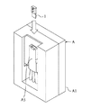
微小粒子測定装置Aには、本体A1のカバーA2によって保護され、更に、ソーティングカバーA3によって保護される微小粒子分取場が設けられている。この微小粒子分取場は、ソーティングカバーA3の上部開口に挿入して取り付けられる、後述するマイクロチップ1を含んで構成される。図2中のブロック矢印は、マイクロチップ1を構成要素とするマイクロチップモジュールのソーティングカバーA3への挿入方向を示す。なお、図3では、便宜上、ソーティングカバーA3の図示を省略し、更に、ソーティングカバーA3に差し込まれたマイクロチップモジュールのうち、マイクロチップ1以外の部分の図示を省略している。
The fine particle measuring device A is provided with a fine particle collecting place protected by the cover A2 of the main body A1 and further protected by the sorting cover A3. This microparticle collection site is configured to include a
微小粒子分取場は、マイクロチップ1と、マイクロチップ1の所定部位に光を照射する光学検出部3と一対の対電極4、3つの回収部(容器51、52、53)を含む。光学検出部3及び対電極4は本体A1に配設されており、容器51〜53は本体A1に着脱可能に取り付けられている。なお、図1〜4において、容器の個数は、便宜上、3つとしているが、本技術ではこれに限定されない。
The microparticle collection site includes a
微小粒子分取場の構成について、図4を参照しながら詳細に説明する。図4には、マイクロチップ1と光学検出部3、対電極4、容器51〜53が示されている。図4中、符号2は、マイクロチップ1上に配設された振動素子を示し、符号6は、グランド接地された接地電極を示す。
The configuration of the fine particle sorting field will be described in detail with reference to FIG. FIG. 4 shows a
マイクロチップ1には、後述するとおり、分取対象とする微小粒子を含む液体(サンプル液)が通流される流路11が形成されている。光学検出部3は、流路11の所定部位に光(測定光)を照射し、流路11を通流する微小粒子から発生する光(測定対象光)を検出する。以下、流路11において光学検出部3からの測定光が照射される部位を「光照射部」と称する。
As will be described later, the
光学検出部3は、従来の微小粒子測定装置と同様の構成にすることができる。具体的には、例えば、レーザー光源と、微小粒子に対してレーザー光を集光・照射する集光レンズやダイクロイックミラー、バンドパスフィルター等からなる照射系と、レーザー光の照射によって微小粒子から発生する測定対象光を検出する検出系と、によって構成される。検出系は、例えば、PMT(photo multiplier tube)や、CCDやCMOS素子等のエリア撮像素子等によって構成される。なお、図4では、光学検出部3として集光レンズのみを示している。また、図4では、照射系と検出系を同一の光学経路により構成されている場合を示したが、照射系と検出系は別個の光学経路により構成されていてもよい。
The
光学検出部3の検出系により検出される測定対象光は、測定光の照射によって微小粒子から発生する光であって、例えば、前方散乱光や側方散乱光、レイリー散乱やミー散乱等の散乱光や蛍光などとすることができる。これらの測定対象光は電気信号に変換され、微小粒子の光学特性は、この電気信号に基づいて検出される。
The measurement target light detected by the detection system of the
光照射部を通過したサンプル液は、流路11の一端に設けられた吐出部12からチップ外の空間に排出される。この際、ピエゾ素子などの振動素子2によってマイクロチップ1を振動させることで、サンプル液を液滴化してチップ外の空間に吐出することができる。図4中、符号Dは、チップ外の空間に吐出された液滴を示している。
The sample liquid that has passed through the light irradiation unit is discharged into the space outside the chip from the
液滴Dには、分取対象とする微小粒子が含まれる。対電極4は、チップ外の空間に吐出された液滴の移動方向に沿って配設されており、移動する液滴を挟んで対向するように配置されている。吐出された液滴には不図示の荷電手段によって電荷が付与され、対電極4は液滴に付与された電荷との電気的な反発力(又は吸引力)によって液滴の移動方向を制御し、液滴を容器51〜53のいずれかに誘導する。
The droplet D contains fine particles to be sorted. The
微小粒子測定装置Aでは、光学検出部3により検出された微小粒子の光学特性に基づいて、その微小粒子が含まれる液滴の移動方向を対電極4により制御することで、所望の特性を備えた微小粒子を容器51〜53のいずれかに回収し、分取することができる。
The fine particle measuring device A has desired characteristics by controlling the moving direction of the droplets containing the fine particles by the
なお、微小粒子測定装置Aにおいて、光学検出部3は、例えば、電気的又は磁気的な検出手段に置換されてもよい。微小粒子の特性を電気的又は磁気的に検出する場合には、流路11に両側に微小電極を対向させて配設し、抵抗値、容量値(キャパシタンス値)、インダクタンス値、インピーダンス、電極間の電界の変化値、或いは磁化、磁界変化、磁場変化等を測定する。この場合、微小粒子の分取は、微小粒子の電気的又は磁気的な特性に基づいて行われる。
In the fine particle measuring device A, the
2.マイクロチップ1
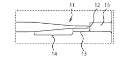
次に、本技術に係るマイクロチップ1について、詳細に説明する。図5は、本技術に係るマイクロチップ1の構成の一例を示す模式図であり、Aは上面模式図、BはA中のP−P断面に対応する断面模式図を示す。また、図6は、図5中の破線で囲まれた部分(図5中のQ参照)の拡大図であり、図7は、図5中のR−R部分拡大図である。更に、図8は、吐出部12を吐出方向から正面視した際の構成の一例を示す模式図である。
2.
Next, the
マイクロチップ1は、液体が通流する流路11と、流路11を通流する前記液体を外部に吐出する吐出部12と、を少なくとも備え、流路11及び吐出部12は、積層された基板層に形成され、図7及び8に示すように、吐出部12は、前記基板層の片側の層にのみ形成されている。また、本技術では、マイクロチップ1は、必要に応じて、更に、検出エリア13、テーパ部14、空洞(キャビティー)15などを備えていてもよい。
The
従来のマイクロチップは、吐出部の断面が基板層の積層水平方向に完全対称であり、例えば、特許文献1(特開2013−32994号公報)に開示されたマイクロチップでは、図12のAに示すように、吐出部の形状は半円形となっていて、基板層を積層した際に円形となるように設計されていた。しかし、基板層を貼り合わせする際に貼りズレが生じることがあり、例えば、図12のBに示すように、半円形がシフトした状態となり、これが液滴形状の対称性や液滴の吐出角度などに影響を与えるため、基板層の貼り合わせを高精度に行うことが必要となり、歩留まりの低下も招いていた。 In the conventional microchip, the cross section of the ejection portion is completely symmetrical in the horizontal direction in which the substrate layers are laminated. For example, in the microchip disclosed in Patent Document 1 (Japanese Unexamined Patent Publication No. 2013-32994), FIG. As shown, the shape of the discharge portion is semi-circular, and it is designed to be circular when the substrate layers are laminated. However, when the substrate layers are bonded together, the bonding may be misaligned. For example, as shown in FIG. 12B, the semicircle is shifted, which is the symmetry of the droplet shape and the ejection angle of the droplet. In order to affect such factors, it is necessary to bond the substrate layers with high accuracy, which also leads to a decrease in yield.
これに対し、本技術では、吐出部12を前記基板層の片側にのみ形成したことで、貼りズレの問題が無くなり、歩留まりの問題も改善されるため、製造バラつきや、それによる性能バラつきを抑えたマイクロチップを提供することができる。
On the other hand, in the present technology, since the
本技術において、吐出部12を吐出方向から正面視した際の形状は、前記基板層に対して垂直方向に左右対称な多角形であることが好ましい。これは、吐出部12が円形であると、金型の加工や、表面の鏡面仕上げが非常に困難であるため、リピート金型を作製する上で再現性よく作製することに対するリスクがあったためである。このようにすることで、金型がより高精度に加工でき、製造バラつきや、それによる性能バラつきをより抑えることが可能となる。また、吐出部12を円形とすると、光が散乱してしまうため、後述する検出エリア13が小さくなってしまう。そのため、このような形状とすることで、後述する検出エリア13が限定されることを防ぐことも可能である。
In the present technology, the shape of the
吐出部12を吐出方向から正面視した際の具体的な形状は特に限定されないが、三角形、四角形、及び六角形からなる群より選ばれるいずれか一つであることが好ましい。このようにすることで、金型がより高精度に加工でき、製造バラつきや、それによる性能バラつきをより抑えることが可能となる。なお、本明細書において、四角形の中には、当然に、台形、長方形、及び正方形が含まれる。
The specific shape of the
また、吐出部12を吐出方向から正面視した際の具体的な形状は、四角形であることがより好ましく、長方形又は正方形とすることが特に好ましい。その理由について、以下に詳細に説明する。
Further, the specific shape of the
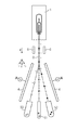
図11は、微小粒子測定装置Aにおける微小粒子の分取動作を説明する模式図であるが、微小粒子測定装置にセットされたマイクロチップから液滴が形成される様子も示している。ここで、従来、液滴がマイクロチップの吐出部から吐出され液滴が形成されるまでの長さ(Break off point:ブレイク・オフ・ポイント、以下、「BOP」と称する)が安定していることが、微小粒子測定装置の性能として非常に重要となることが知られている。 FIG. 11 is a schematic view illustrating the operation of separating fine particles in the fine particle measuring device A, but also shows how droplets are formed from the microchip set in the fine particle measuring device. Here, conventionally, the length until the droplet is ejected from the ejection portion of the microchip and the droplet is formed (Break off point, hereinafter referred to as “BOP”) is stable. It is known that this is very important for the performance of the microparticle measuring device.
図9は、吐出部の形状の違いによる液滴の形状確認を行った様子を示す図であり、Aは本技術の吐出部12の形状(四角形)で、Bは従来の吐出部12の形状で、それぞれ、液滴の形状確認を行った様子を示している。図9のA及びBに記載のグラフ中、縦軸はBOPの高さ(a.u.)を示し、横軸はピエゾ圧電素子の周波数(Hz)を示す。
FIG. 9 is a diagram showing a state in which the shape of the droplet is confirmed due to the difference in the shape of the discharge portion. A is the shape (square) of the
図9の結果から、いずれの形状においても、液滴が綺麗に形成されていることが分かる。しかし、図9のAに示すように、液体に対して同一なタンク圧力条件において、本技術の吐出部の形状(四角形)の方が、液滴が安定して形成される周波数帯域が広くなっている。また、BOPの高さはチップの流量ばらつきに起因するため、基板層の貼り合せ条件を調整し、流量を合わせこんでも、周波数に対する液滴安定性は本技術の吐出部の形状(四角形)の方が良好であった。 From the result of FIG. 9, it can be seen that the droplets are neatly formed in any of the shapes. However, as shown in A of FIG. 9, under the same tank pressure condition for the liquid, the shape (square) of the discharge portion of the present technology has a wider frequency band in which droplets are stably formed. ing. Further, since the height of the BOP is caused by the variation in the flow rate of the chip, even if the bonding conditions of the substrate layers are adjusted and the flow rate is adjusted, the droplet stability with respect to the frequency is the shape (square) of the ejection part of the present technology. Was better.
また、図9のBに示すように、従来の吐出部12の形状では、小液滴が後続する主液滴に追いつかれる低速サテライト(slow satellite)しか形成できなかったが、図9のAに示すように、本技術の吐出部の形状(四角形)では、小液滴が先行する主液滴に追いつく高速サテライト(fast satellite)と低速サテライトの両方を形成することができた。
Further, as shown in B of FIG. 9, in the conventional shape of the
なお、本明細書において、「サテライト(satellite)」とは、液滴吐出後に後部に引き伸ばされた細い棒状の液柱が表面張力によって主液滴とノズルから分離する際に形成される小液滴のことであり、このサテライトは、液滴のチャージ変動の要因となるため、インクジェットプリンターやソータのような、液滴の偏向位置精度を要求する微小粒子測定装置にとっては、制御が不可欠なパラメータの1つとなっていることが知られている。 In addition, in this specification, a "satellite" is a small droplet formed when a thin rod-shaped liquid column stretched to the rear after ejection of a droplet is separated from a main droplet and a nozzle by surface tension. Since this satellite causes fluctuations in the charge of droplets, control is an indispensable parameter for fine particle measuring devices that require accuracy in the deflection position of droplets, such as inkjet printers and sorters. It is known to be one.
高速サテライトが形成されることにより、低速サテライトが形成されている場合と比較してチャージ変動に対するマージンがあるため、サイドストリームが安定し、しぶきを低減できるという効果がある。本技術では、図9のAに示すように、高速サテライトと低速サテライトの両方を周波数条件によって安定して使い分けることができるため、低速サテライトしか形成できなかった従来技術と比較して非常に有用である。 Since the high-speed satellite is formed, there is a margin for charge fluctuation as compared with the case where the low-speed satellite is formed, so that there is an effect that the side stream is stable and the splash can be reduced. In this technology, as shown in A of FIG. 9, both high-speed satellites and low-speed satellites can be stably used depending on the frequency conditions, which is very useful as compared with the conventional technology in which only low-speed satellites can be formed. be.
本技術において、吐出部12を構成する一辺の長さは特に限定されないが、50μm〜300μmであることが好ましい。これにより、前述した微小粒子測定装置Aに好適に用いることができる。
In the present technology, the length of one side constituting the
また、吐出部12を吐出方向から正面視した際の具体的な形状は、前述のとおり、四角形であることが望ましいが、角形状は金型の加工精度に応じて丸み(R)を加えてもよい。この場合、一辺の長さの1%〜20%の角Rを見込んでも構わない。
Further, as described above, the specific shape of the
本技術に係るマイクロチップ1は、例えば、流路11が形成された基板層1a、1bが貼り合わされてなる。基板層1a、1bへの流路11の形成は、金型を用いた熱可塑性樹脂の射出成形により行うことができる。なお、流路11は、基板層1a、1bのどちらか一方のみに形成されていてもよく、基板層1a、1bの双方にそれぞれ形成されていてもよい。
The
熱可塑性樹脂には、ポリカーボネート、ポリメタクリル酸メチル樹脂(PMMA)、環状ポリオレフィン、ポリエチレン、ポリスチレン、ポリプロピレン及びポリメチルジシラザン(PDMS)などの、従来マイクロチップの材料として公知のものを適宜自由に選択できる。 As the thermoplastic resin, conventionally known materials for microchips such as polycarbonate, polymethylmethacrylate resin (PMMA), cyclic polyolefin, polyethylene, polystyrene, polypropylene and polymethyldisilazane (PDMS) can be freely selected as appropriate. can.
射出成形は、従来公知の手法によって行うことができる。例えば、射出成形装置(住友重機械工業株式会社製、SE75DU)を用いてポリオレフィン(日本ゼオン株式会社、ZEONEX1060R)を射出成形する場合、典型的な成形条件としては、樹脂温度270℃、金型温度80℃、型締め力500kNが用いられる。 Injection molding can be performed by a conventionally known method. For example, when a polyolefin (ZEON EX1060R) is injection-molded using an injection molding device (SE75DU manufactured by Sumitomo Heavy Industries, Ltd.), typical molding conditions are a resin temperature of 270 ° C. and a mold temperature. 80 ° C. and a mold clamping force of 500 kN are used.
このように、本技術に係るマイクロチップ1は、高価な石英、及び、アルミナ及びジルコニア等のセラミックなどの研磨加工によることなく、熱可塑性樹脂の射出成形及び熱圧着によって、流路11及び吐出部12を形成できるため、安価で量産性に優れる。
As described above, the
また、流路11が形成された基板層1a、1bの貼り合わせは、従来公知の手法によって熱圧着することによって行うことができる。例えば、前述したポリオレフィン基板層を、ナノインプリント装置(キャノン株式会社、Eitre 6/8)を用いて熱圧着する場合、典型的な圧着条件としては、貼り合わせ温度95℃、押圧力10kNで数分間の押圧が用いられる。
Further, the substrate layers 1a and 1b on which the
サンプル液は、サンプルインレットM1から導入され、シースインレットM2から導入されるシース液と合流して、流路11を送液される。シースインレットM2から導入されたシース液は、2方向に分かれて送液された後、サンプルインレットM1から導入されたサンプル液との合流部において、サンプル液を2方向から挟み込むようにしてサンプル液に合流する。これにより、合流部において、シース液層流の中央にサンプル液層流が位置された3次元層流が形成される。
The sample liquid is introduced from the sample inlet M1 and merges with the sheath liquid introduced from the sheath inlet M2, and is sent to the
符号M3は、流路11に詰まりや気泡が生じた際に、流路11内に負圧を加えて流れを一時的に逆流させて詰まりや気泡を解消するための吸引流路を示す。吸引流路M3の一端には、真空ポンプ等の負圧源が接続される吸引アウトレットM31が形成され、他端は連通口M32において流路11に接続している。
Reference numeral M3 indicates a suction flow path for clearing the clogging or air bubbles by applying a negative pressure to the
3次元層流は、送液方向に対する垂直断面の面積が送液方向上流から下流へ次第に、或いは段階的に小さくなるように形成された絞込部M4(図5及び10参照)において層流幅を絞り込まれた後、流路の一端に設けられた吐出部12から排出される。図10に、吐出部12からチップ外の空間に吐出された液滴Dを示す。図10中、符号Pは、微小粒子を示し、符号Fは、吐出部12からの液滴Dの吐出方向を示す。
The three-dimensional laminar flow is the laminar flow width in the narrowing portion M4 (see FIGS. 5 and 10) formed so that the area of the cross section perpendicular to the liquid feeding direction gradually decreases from the upstream to the downstream in the liquid feeding direction. Is narrowed down and then discharged from the
本技術では、流路11のうち吐出部12への接続部には、図6に示すように、流路11を通流するサンプルを光学的に検出する検出エリア13を更に有し、検出エリア13から吐出部12までの流路深さは、一定であるものとすることができる。これにより、検出エリア13の開始地点から吐出部12までの間であれば、どの位置でも検出を行うことが可能となる。なお、性能としては、吐出部12に近づくほど、細胞の種類やサイズなどによる速度バラつきは低減する。
In the present technology, as shown in FIG. 6, the connection portion of the
また、本技術では、流路11は、図6に示すように、検出エリア13に連通するテーパ部14を更に有していることが好ましい。これにより、細胞の種類やサイズなどによる速度バラつきの低減を図ることができる。
Further, in the present technology, it is preferable that the
吐出部12は、前述のとおり、基板層1a又は基板層1bのいずれか一方に形成され、すなわち、いずれかの基板層の端面方向に開口しているが、本技術に係るマイクロチップ1は、この吐出部12に連通し、吐出部12から吐出される液滴を空間的に覆う空洞(キャビティー)15を更に備えていてもよい。空洞15は、例えば、吐出部12と基板端面との間の基板層1a、1bを、空洞15の径L1が吐出部12の径L2よりも大きくなるように切り欠くことによって形成することができる(図8参照)。
As described above, the
本技術に係るマイクロチップ1が、空洞15を備えることにより、基板層の射出成形及び熱圧着に起因した吐出部12及び流路11の形状の不整や変形が生じることがなくなる。したがって、本技術に係るマイクロチップ1では、均一な形状の吐出部12から一定の大きさ及び形状の液滴を一定の方向に真っ直ぐに吐出できる。更に、吐出部12がチップ端面に存在しなくなるため、製造プロセスにおける不慮の接触などによる吐出部12の破壊が起こり難く、高い生産性が得られる。
When the
空洞15の径L1は、図8に示すように、吐出部12から吐出される液滴の移動を阻害しないように、吐出部15の径L2よりも2倍以上大きく形成することが好ましい。ただし、空洞15の径L1をあまりに大きくし過ぎると、基板層1a、1bを熱圧着する際の熱分布及び圧力分布の均一性が悪くなったり、空洞15内に「ガス」が溜まったりして、吐出部12の形状不整の原因となる。
As shown in FIG. 8, the diameter L1 of the
図8及び10では、空洞15を八角柱形状に基板層1a、1bを切り欠いて形成する場合を示しているが、本技術では、空洞15の形状は、吐出部12から吐出される液滴を空間的に覆うことができれば特に限定されない。また、空洞15は、吐出部12と同軸上に設けることが好ましいが、これに限定されることはない。また、マイクロチップ1の厚さが薄い場合などには、空洞15は、基板層1a、1bを厚み方向に全層切欠いて形成してもよい。
8 and 10 show a case where the
ここで、従来、基板層を射出成形する際、熱可塑性樹脂の金型に接する部分で、「ばり」、或いは「だれ」と称される成形不良が発生することが知られている。また、特に、成形時に発生する「ガス」は、成形後に基板層の端面となる部分及びその周辺の形状を著しく変形させる。このため、吐出部12を基板層端面に設ける場合には、成形不良の影響によって吐出部12の形状が不整となりやすい。
Here, conventionally, when the substrate layer is injection-molded, it is known that a molding defect called "burr" or "who" occurs at a portion of the thermoplastic resin in contact with the mold. In particular, the "gas" generated during molding significantly deforms the shape of the end face of the substrate layer and its surroundings after molding. Therefore, when the
このため、本技術では、マイクロチップ1が空洞15を備えることにより、吐出部12を基板層端面から所定長陥凹した位置に設けている。その結果、基板層端面及びその周辺で仮に成形不良が生じたとしても、吐出部12の形状には影響が及ばない。したがって、マイクロチップ1では、吐出部12の形状を所望の形状に安定して成形することができ、吐出部12から一定の大きさ及び形状を有する液滴が吐出されるようにすることができる。
Therefore, in the present technology, the
吐出部12から空洞15の端までの長さ(図7のW参照)は、0.2mm以上とすることが好ましい。これにより、基板層端面及びその周辺で生じる成形不良の影響を完全に排除することができる。また、この場合、本技術に係るマイクロチップ1のサイズは特に限定されず、例えば、横75mm×縦25mm×厚さ2mmなどにすることができる。
The length from the
更に、従来、基板層を熱圧着する際、基板層の端面及び辺縁では、基板層の中央に比べて熱収縮による変形が大きくなることが知られている。このため、吐出部12やこれに接続する流路を基板端面及びその近傍に設ける場合には、熱収縮によって成形された吐出部12の形状や流路の形状が変形しやすい。
Further, conventionally, when the substrate layer is thermocompression bonded, it is known that the end face and the edge of the substrate layer are deformed more due to heat shrinkage than the center of the substrate layer. Therefore, when the
これに対し、本技術では、マイクロチップ1が空洞15を備えることにより、吐出部12が基板層端面から所定長内側とされている。その結果、基板層の熱圧着時に吐出部12の形状及びこれに接続する検出エリア13の形状が変形することがない。したがって、マイクロチップ1では、吐出部12の形状及び検出エリア13の形状を所望の形状に維持し、吐出部12から一定の大きさ及び形状を有する液滴Dが真っ直ぐに吐出されるようにできる。
On the other hand, in the present technology, since the
本技術に係るマイクロチップ1の用途は特に限定されないが、後述するとおり、微小粒子の測定に好適に用いられる。
The application of the
3.微小粒子測定装置Aの動作
最後に、微小粒子分析装置Aの動作について、図11を参照しながら説明する。
3. 3. Operation of Microparticle Measuring Device A Finally, the operation of the microparticle analyzer A will be described with reference to FIG.
流路11の光照射部を通過したサンプル液及びシース液は、吐出部12からチップ外の空間に排出される。光照射部では、光学検出部によって、微小粒子の光学特性の検出と同時に、微小粒子の送流速度(流速)及び微小粒子の間隔などの検出が行われている。検出された微小粒子の光学特性、流速及び間隔等は電気的信号に変換され、装置の全体制御部(不図示)に出力される。全体制御部は、この信号に基づいて振動素子2(図4参照)の振動数を制御し、吐出部12において形成される液滴D中に微小粒子Pがひとつずつ含まれるようにマイクロチップ1を振動させる。
The sample liquid and the sheath liquid that have passed through the light irradiation portion of the
更に、全体制御部は、振動素子2の振動周波数に同調させて、流路11を通流するシース液及びサンプル液に付与される電荷の正負を切り換え、吐出部12において形成される液滴Dに正又は負の電荷を付与する。
Further, the overall control unit switches the positive and negative charges applied to the sheath liquid and the sample liquid flowing through the
光学検出部によって検出された微小粒子の光学特性は、電気信号に変換されて全体制御部に出力される。全体制御部は、この信号に基づき、各液滴に含まれる微小粒子の光学特性に応じて液滴に付与する電荷を決定する。具体的には、全体制御部は、例えば、所望の特性を有する分取対象微小粒子を含む液滴を正に、分取対象微小粒子を含まない液滴を負に帯電させる。 The optical characteristics of the fine particles detected by the optical detection unit are converted into an electric signal and output to the overall control unit. Based on this signal, the overall control unit determines the charge to be applied to the droplet according to the optical characteristics of the fine particles contained in each droplet. Specifically, for example, the overall control unit positively charges the droplet containing the fine particles to be sorted with the desired characteristics, and negatively charges the droplet containing the fine particles to be sorted.
この際、液滴Dの荷電状態を安定化させるため、微小粒子分析装置Aでは、吐出部12近傍に、チップ外の空間に吐出された液滴の移動方向に沿って、接地電極6を配置している。接地電極6は、移動する液滴を挟んで対向するように配置されており、微小粒子の移動方向を制御するための対電極4と吐出部12との間に配設される。
At this time, in order to stabilize the charged state of the droplet D, in the fine particle analyzer A, the
吐出部12から荷電されて吐出される液滴Dは、対電極4との間に作用する電気的力によって移動方向を制御される。この際、移動方向の制御を正確に行うためには、安定した電荷が液滴に付与されていることが必要である。対電極4には、非常に高い電圧が印加されるため、対電極4の高電位が液滴Dに付与される電荷に影響を与えると、液滴Dの荷電状態が不安定になるおそれがある。そこで、微小粒子測定装置Aでは、吐出部12と対電極4との間に接地された接地電極6を配することで、このような対電極4の高電位による影響を排除している。
The moving direction of the droplet D charged and discharged from the
吐出部12から吐出される液滴Dの移動方向の制御は、例えば、以下のように行われる。すなわち、所望の特性を有する分取対象微小粒子が含まれる液滴を正に、分取対象微小粒子を含まない液滴を負に帯電させる先の例では、対電極4の一方を正に、対電極4の他方を負に帯電させることにより、分取対象微小粒子のみを容器53に分取することができる。より具体的には、正電荷が付与された分取対象微小粒子を含む液滴は、対電極4の一方との電気的反発力及び対電極4の他方との電気的吸引力によって、移動方向を矢印f3方向に制御され容器53に誘導される。一方で、負電荷が付与された分取対象微小粒子を含まない液滴は、移動方向を矢印f2方向に制御され容器52に誘導される。
The movement direction of the droplet D discharged from the
或いは、例えば、所望の特性を有する分取対象微小粒子が含まれる液滴に電荷を付与せず、分取対象微小粒子を含まない液滴を正又は負に帯電させ、対電極4を正又は負に帯電させれば、分取対象微小粒子のみを容器51に分取することができる。その他、液滴Dに付与する電荷と、対電極4による液滴の移動方向の制御は、従来のフローサイトメトリーと同様に様々な組合せにおいて行うことができる。なお、微小粒子測定装置Aにおいて、液滴Dを回収するための容器は、通常2つ以上設けられているが、図11に示すように、3つに限定されるものではない。更に、これらの容器は、回収した液滴を貯留することなく排出する排出路として構成されていてもよく、回収された分取対象でない微小粒子が破棄されるようにしてもよい。
Alternatively, for example, the droplet containing the fine particles to be sorted having the desired characteristics is not charged, the droplet not containing the fine particles to be sorted is positively or negatively charged, and the
前述のとおり、マイクロチップ1では、均一な形状の吐出部12から一定の大きさ及び形状の液滴Dを一定の方向に真っ直ぐに吐出できる。このため、微小粒子測定装置Aでは、液滴Dの移動方向の制御を高精度に行うことができ、所望の特性を有する微小粒子を正確に分取することが可能とされている。
As described above, in the
ここでは、液滴Dに、その液滴に含まれる微小粒子の特性に基づいて正又は負の電荷を切り換えて付与して分取を行う場合を例に説明している。しかし、液滴の分取は、光学検出部を電気的又は磁気的な検出手段に置換した場合においても、微小粒子の電気的又は磁気的特性に基づき同様にして液滴の移動方向を制御することで、所望の特性を備えた微小粒子を容器51〜53のいずれかに回収し、分取することが可能である。
Here, a case where positive or negative charges are switched and applied to the droplet D based on the characteristics of the fine particles contained in the droplet and the droplet D is subjected to sorting will be described as an example. However, the fractionation of the droplets controls the moving direction of the droplets in the same manner based on the electrical or magnetic characteristics of the fine particles even when the optical detection unit is replaced with an electrical or magnetic detection means. As a result, the fine particles having the desired characteristics can be collected in any of the
なお、本技術では、以下の構成を取ることもできる。
(1)
液体が通流する流路と、
該流路を通流する前記液体を外部に吐出する吐出部と、
を少なくとも備え、
前記流路及び前記吐出部は、積層された基板層に形成され、
前記吐出部は、前記基板層の片側の層にのみ形成されているマイクロチップ。
(2)
前記吐出部を吐出方向から正面視した際の形状が、前記基板層に対して垂直方向に左右対称な多角形である、(1)に記載のマイクロチップ。
(3)
前記形状は、三角形、四角形、及び六角形からなる群より選ばれるいずれか一つである、(2)に記載のマイクロチップ。
(4)
前記吐出部を構成する一辺の長さは、50μm〜300μmである、(2)又は(3)に記載のマイクロチップ。
(5)
前記流路は、該流路を通流するサンプルを光学的に検出する検出エリアを更に有し、
前記検出エリアから前記吐出部までの流路深さは、一定である、(1)から(4)のいずれかに記載のマイクロチップ。
(6)
前記流路は、前記検出エリアに連接するテーパ部を更に有する、(5)に記載のマイクロチップ。
(7)
前記吐出部に連通し、前記吐出部から吐出される液滴を空間的に覆う空洞を更に備える、(1)から(6)のいずれかに記載のマイクロチップ。
(8)
前記吐出部から前記空洞の端までの長さは、0.2mm以上である、(7)に記載のマイクロチップ。
(9)
微小粒子の測定に用いられる、(1)から(8)のいずれかに記載のマイクロチップ。
(10)
(1)から(9)のいずれかに記載のマイクロチップが搭載された微小粒子測定装置。
The present technology can also have the following configurations.
(1)
The flow path through which the liquid flows and
A discharge unit that discharges the liquid flowing through the flow path to the outside,
At least
The flow path and the discharge portion are formed in a laminated substrate layer, and the flow path and the discharge portion are formed in a laminated substrate layer.
The discharge portion is a microchip formed only on one side of the substrate layer.
(2)
The microchip according to (1), wherein the shape of the discharge portion when viewed from the front from the discharge direction is a polygon that is symmetrical in the direction perpendicular to the substrate layer.
(3)
The microchip according to (2), wherein the shape is any one selected from the group consisting of a triangle, a quadrangle, and a hexagon.
(4)
The microchip according to (2) or (3), wherein the length of one side constituting the discharge portion is 50 μm to 300 μm.
(5)
The flow path further has a detection area for optically detecting a sample flowing through the flow path.
The microchip according to any one of (1) to (4), wherein the flow path depth from the detection area to the discharge portion is constant.
(6)
The microchip according to (5), wherein the flow path further has a tapered portion connected to the detection area.
(7)
The microchip according to any one of (1) to (6), further comprising a cavity that communicates with the discharge portion and spatially covers the droplet discharged from the discharge portion.
(8)
The microchip according to (7), wherein the length from the discharge portion to the end of the cavity is 0.2 mm or more.
(9)
The microchip according to any one of (1) to (8), which is used for measuring fine particles.
(10)
A microparticle measuring device on which the microchip according to any one of (1) to (9) is mounted.
1:マイクロチップ
11:流路
12:吐出部
13:検出エリア
14:テーパ部
15:空洞(キャビティー)
1a、1b:基板層
M1:サンプルインレット
M2:シースインレット
M3:吸引流路
M31:吸引アウトレット
M32:連通口
M4:絞込部
2:振動素子
3:光学検出部
4:対電極
51、52、53:回収部(容器)
6:接地電極
A:微小粒子測定装置
A1:本体
A2:カバー
A3:ソーティングカバー
D:液滴
P:微小粒子
1: Microchip 11: Flow path 12: Discharge part 13: Detection area 14: Tapered part 15: Cavity
1a, 1b: Substrate layer M1: Sample inlet M2: Sheath inlet M3: Suction flow path M31: Suction outlet M32: Communication port M4: Narrowing part 2: Vibration element 3: Optical detection part 4:
6: Ground electrode A: Fine particle measuring device A1: Main body A2: Cover A3: Sorting cover D: Droplet P: Fine particles
Claims (12)
該流路を通流する前記液体を外部に吐出する吐出部と、
を少なくとも備え、
前記流路及び前記吐出部は、積層された基板層に形成され、
前記吐出部は、前記基板層の片側の層にのみ形成され、
前記吐出部を吐出方向から正面視した際の形状が、四角形であるマイクロチップ。 The flow path through which the liquid flows and
A discharge unit that discharges the liquid flowing through the flow path to the outside,
At least
The flow path and the discharge portion are formed in a laminated substrate layer, and the flow path and the discharge portion are formed in a laminated substrate layer.
The discharge portion is formed only on one side of the substrate layer, and is formed .
Wherein the discharge portion is shaped when viewed from the front from the ejection direction, rectangle der Ru microchip.
前記検出エリアから前記吐出部までの流路深さは、一定である、請求項1から3のいずれか一項に記載のマイクロチップ。 The flow path further has a detection area for optically detecting a sample flowing through the flow path.
The microchip according to any one of claims 1 to 3 , wherein the flow path depth from the detection area to the discharge portion is constant.
前記液体を液滴化するために振動を加える振動素子と、A vibrating element that applies vibration to atomize the liquid,
前記液滴に電荷を与える電荷部と、The charged part that gives a charge to the droplet and
前記振動素子及び前記電荷部を制御する制御部と、A control unit that controls the vibrating element and the charge unit,
を少なくとも備え、At least
前記マイクロチップにおける前記流路及び前記吐出部は、積層された基板層に形成され、The flow path and the discharge portion of the microchip are formed in a laminated substrate layer.
前記吐出部は、前記基板層の片側の層にのみ形成され、The discharge portion is formed only on one side of the substrate layer, and is formed.
前記吐出部を吐出方向から正面視した際の形状が、四角形である微小粒子測定装置。A fine particle measuring device having a quadrangular shape when the discharge portion is viewed from the front from the discharge direction.
前記制御部は、前記小液滴が高速サテライトとして形成されるよう前記振動素子を制御する、請求項10に記載の微小粒子測定装置。The fine particle measuring device according to claim 10, wherein the control unit controls the vibrating element so that the small droplets are formed as high-speed satellites.
Priority Applications (6)
| Application Number | Priority Date | Filing Date | Title |
|---|---|---|---|
| JP2017049011A JP6922281B2 (en) | 2017-03-14 | 2017-03-14 | Microchip and fine particle measuring device |
| US16/490,138 US20200070152A1 (en) | 2017-03-14 | 2018-02-27 | Microchip and microparticle measuring apparatus |
| EP18720027.4A EP3595814A1 (en) | 2017-03-14 | 2018-02-27 | Microchip and microparticle measuring apparatus |
| CN201880016751.9A CN110382117B (en) | 2017-03-14 | 2018-02-27 | Microchip and microparticle measuring device |
| PCT/JP2018/007158 WO2018168436A1 (en) | 2017-03-14 | 2018-02-27 | Microchip and microparticle measuring apparatus |
| US17/959,491 US20230063086A1 (en) | 2017-03-14 | 2022-10-04 | Microchip and microparticle measuring apparatus |
Applications Claiming Priority (1)
| Application Number | Priority Date | Filing Date | Title |
|---|---|---|---|
| JP2017049011A JP6922281B2 (en) | 2017-03-14 | 2017-03-14 | Microchip and fine particle measuring device |
Publications (3)
| Publication Number | Publication Date |
|---|---|
| JP2018151319A JP2018151319A (en) | 2018-09-27 |
| JP2018151319A5 JP2018151319A5 (en) | 2020-03-05 |
| JP6922281B2 true JP6922281B2 (en) | 2021-08-18 |
Family
ID=62046995
Family Applications (1)
| Application Number | Title | Priority Date | Filing Date |
|---|---|---|---|
| JP2017049011A Active JP6922281B2 (en) | 2017-03-14 | 2017-03-14 | Microchip and fine particle measuring device |
Country Status (5)
| Country | Link |
|---|---|
| US (2) | US20200070152A1 (en) |
| EP (1) | EP3595814A1 (en) |
| JP (1) | JP6922281B2 (en) |
| CN (1) | CN110382117B (en) |
| WO (1) | WO2018168436A1 (en) |
Families Citing this family (6)
| Publication number | Priority date | Publication date | Assignee | Title |
|---|---|---|---|---|
| US11796449B2 (en) | 2013-10-30 | 2023-10-24 | Abs Global, Inc. | Microfluidic system and method with focused energy apparatus |
| JP2018509615A (en) | 2015-02-19 | 2018-04-05 | プレミアム ジェネティクス (ユーケー) リミテッド | Scanning infrared measurement system |
| JP6919215B2 (en) | 2017-02-17 | 2021-08-18 | ソニーグループ株式会社 | Microchip and fine particle sorter |
| US11889830B2 (en) | 2019-04-18 | 2024-02-06 | Abs Global, Inc. | System and process for continuous addition of cryoprotectant |
| US11628439B2 (en) * | 2020-01-13 | 2023-04-18 | Abs Global, Inc. | Single-sheath microfluidic chip |
| WO2023238564A1 (en) * | 2022-06-10 | 2023-12-14 | ソニーグループ株式会社 | Information processing system, information processing method, information processing device, and program |
Family Cites Families (10)
| Publication number | Priority date | Publication date | Assignee | Title |
|---|---|---|---|---|
| JP2832117B2 (en) * | 1991-11-29 | 1998-12-02 | キヤノン株式会社 | Sample measuring device and sample measuring system |
| WO2007009125A2 (en) * | 2005-07-14 | 2007-01-18 | Nano-Ditech Corporation | Microfluidic devices and methods of preparing and using the same |
| JP5487638B2 (en) * | 2009-02-17 | 2014-05-07 | ソニー株式会社 | Apparatus for microparticle sorting and microchip |
| JP2011237201A (en) * | 2010-05-06 | 2011-11-24 | Sony Corp | Particulate dispensing device, microchip, and microchip module |
| JP5859974B2 (en) * | 2010-10-29 | 2016-02-16 | コニカミノルタ株式会社 | Microchip and manufacturing method of microchip |
| JP6003020B2 (en) * | 2011-08-03 | 2016-10-05 | ソニー株式会社 | Microchip and fine particle analyzer |
| CN105556279B (en) * | 2013-07-16 | 2019-11-26 | 普里米欧姆遗传学(英国)有限公司 | Micro-fluid chip |
| US8961904B2 (en) * | 2013-07-16 | 2015-02-24 | Premium Genetics (Uk) Ltd. | Microfluidic chip |
| CN105659069B (en) * | 2013-10-16 | 2019-11-26 | 索尼公司 | Particle point takes equipment, particle point to take method and program |
| JP6733909B2 (en) * | 2013-10-30 | 2020-08-05 | エービーエス グローバル インコーポレイテッド | Device for identifying multiple substances, computer system for identifying multiple substances, program for causing a computer to execute multiple instructions for identifying multiple substances, and method for identifying multiple substances flowing in a sample fluid mixture |
-
2017
- 2017-03-14 JP JP2017049011A patent/JP6922281B2/en active Active
-
2018
- 2018-02-27 EP EP18720027.4A patent/EP3595814A1/en active Pending
- 2018-02-27 WO PCT/JP2018/007158 patent/WO2018168436A1/en unknown
- 2018-02-27 CN CN201880016751.9A patent/CN110382117B/en active Active
- 2018-02-27 US US16/490,138 patent/US20200070152A1/en not_active Abandoned
-
2022
- 2022-10-04 US US17/959,491 patent/US20230063086A1/en active Pending
Also Published As
| Publication number | Publication date |
|---|---|
| JP2018151319A (en) | 2018-09-27 |
| CN110382117B (en) | 2022-09-27 |
| WO2018168436A1 (en) | 2018-09-20 |
| US20230063086A1 (en) | 2023-03-02 |
| CN110382117A (en) | 2019-10-25 |
| EP3595814A1 (en) | 2020-01-22 |
| US20200070152A1 (en) | 2020-03-05 |
Similar Documents
| Publication | Publication Date | Title |
|---|---|---|
| JP6003020B2 (en) | Microchip and fine particle analyzer | |
| JP6922281B2 (en) | Microchip and fine particle measuring device | |
| KR101850548B1 (en) | Microparticle sorting apparatus, microchip module, and method of sorting microparticles | |
| JP5487638B2 (en) | Apparatus for microparticle sorting and microchip | |
| JP4661942B2 (en) | Microchip and its channel structure | |
| JP5601424B2 (en) | Microparticle sorting apparatus and fluid stream optimization method in the apparatus | |
| JP5994337B2 (en) | Fine particle sorting device and delay time determination method | |
| JP5720233B2 (en) | Microchip and fine particle sorting device | |
| KR20090130811A (en) | Micro-fluidic chip and flow sending method in micro-fluidic chip | |
| WO2010146778A1 (en) | Substance mixing device and substance mixing method | |
| JP2021517640A (en) | Fine particle analyzer and fine particle analysis method | |
| JP5905317B2 (en) | Calibration method and apparatus for fine particle sorting apparatus | |
| JP5316530B2 (en) | Microchip and its channel structure | |
| WO2015111293A1 (en) | Particle sorter and method for sorting particles | |
| JP6965953B2 (en) | Microchip and fine particle analyzer |
Legal Events
| Date | Code | Title | Description |
|---|---|---|---|
| A521 | Request for written amendment filed |
Free format text: JAPANESE INTERMEDIATE CODE: A523 Effective date: 20200124 |
|
| A621 | Written request for application examination |
Free format text: JAPANESE INTERMEDIATE CODE: A621 Effective date: 20200124 |
|
| A131 | Notification of reasons for refusal |
Free format text: JAPANESE INTERMEDIATE CODE: A131 Effective date: 20210105 |
|
| A521 | Request for written amendment filed |
Free format text: JAPANESE INTERMEDIATE CODE: A523 Effective date: 20210303 |
|
| TRDD | Decision of grant or rejection written | ||
| A01 | Written decision to grant a patent or to grant a registration (utility model) |
Free format text: JAPANESE INTERMEDIATE CODE: A01 Effective date: 20210629 |
|
| A61 | First payment of annual fees (during grant procedure) |
Free format text: JAPANESE INTERMEDIATE CODE: A61 Effective date: 20210712 |
|
| R151 | Written notification of patent or utility model registration |
Ref document number: 6922281 Country of ref document: JP Free format text: JAPANESE INTERMEDIATE CODE: R151 |