JP6898570B2 - Semiconductor integrated circuit equipment - Google Patents
Semiconductor integrated circuit equipment Download PDFInfo
- Publication number
- JP6898570B2 JP6898570B2 JP2018520810A JP2018520810A JP6898570B2 JP 6898570 B2 JP6898570 B2 JP 6898570B2 JP 2018520810 A JP2018520810 A JP 2018520810A JP 2018520810 A JP2018520810 A JP 2018520810A JP 6898570 B2 JP6898570 B2 JP 6898570B2
- Authority
- JP
- Japan
- Prior art keywords
- power supply
- wiring
- strap
- switch
- supply wirings
- Prior art date
- Legal status (The legal status is an assumption and is not a legal conclusion. Google has not performed a legal analysis and makes no representation as to the accuracy of the status listed.)
- Active
Links
Images


Classifications
-
- H—ELECTRICITY
- H10—SEMICONDUCTOR DEVICES; ELECTRIC SOLID-STATE DEVICES NOT OTHERWISE PROVIDED FOR
- H10D—INORGANIC ELECTRIC SEMICONDUCTOR DEVICES
- H10D89/00—Aspects of integrated devices not covered by groups H10D84/00 - H10D88/00
- H10D89/10—Integrated device layouts
-
- G—PHYSICS
- G06—COMPUTING OR CALCULATING; COUNTING
- G06F—ELECTRIC DIGITAL DATA PROCESSING
- G06F1/00—Details not covered by groups G06F3/00 - G06F13/00 and G06F21/00
- G06F1/26—Power supply means, e.g. regulation thereof
-
- G—PHYSICS
- G06—COMPUTING OR CALCULATING; COUNTING
- G06F—ELECTRIC DIGITAL DATA PROCESSING
- G06F30/00—Computer-aided design [CAD]
- G06F30/30—Circuit design
- G06F30/39—Circuit design at the physical level
-
- G—PHYSICS
- G06—COMPUTING OR CALCULATING; COUNTING
- G06F—ELECTRIC DIGITAL DATA PROCESSING
- G06F30/00—Computer-aided design [CAD]
- G06F30/30—Circuit design
- G06F30/39—Circuit design at the physical level
- G06F30/392—Floor-planning or layout, e.g. partitioning or placement
-
- G—PHYSICS
- G06—COMPUTING OR CALCULATING; COUNTING
- G06F—ELECTRIC DIGITAL DATA PROCESSING
- G06F30/00—Computer-aided design [CAD]
- G06F30/30—Circuit design
- G06F30/39—Circuit design at the physical level
- G06F30/394—Routing
-
- H—ELECTRICITY
- H03—ELECTRONIC CIRCUITRY
- H03K—PULSE TECHNIQUE
- H03K19/00—Logic circuits, i.e. having at least two inputs acting on one output; Inverting circuits
- H03K19/0008—Arrangements for reducing power consumption
- H03K19/0016—Arrangements for reducing power consumption by using a control or a clock signal, e.g. in order to apply power supply
-
- H—ELECTRICITY
- H10—SEMICONDUCTOR DEVICES; ELECTRIC SOLID-STATE DEVICES NOT OTHERWISE PROVIDED FOR
- H10D—INORGANIC ELECTRIC SEMICONDUCTOR DEVICES
- H10D84/00—Integrated devices formed in or on semiconductor substrates that comprise only semiconducting layers, e.g. on Si wafers or on GaAs-on-Si wafers
- H10D84/90—Masterslice integrated circuits
- H10D84/903—Masterslice integrated circuits comprising field effect technology
- H10D84/907—CMOS gate arrays
-
- H10W20/427—
-
- H—ELECTRICITY
- H10—SEMICONDUCTOR DEVICES; ELECTRIC SOLID-STATE DEVICES NOT OTHERWISE PROVIDED FOR
- H10D—INORGANIC ELECTRIC SEMICONDUCTOR DEVICES
- H10D84/00—Integrated devices formed in or on semiconductor substrates that comprise only semiconducting layers, e.g. on Si wafers or on GaAs-on-Si wafers
- H10D84/90—Masterslice integrated circuits
- H10D84/903—Masterslice integrated circuits comprising field effect technology
- H10D84/907—CMOS gate arrays
- H10D84/968—Macro-architecture
- H10D84/974—Layout specifications, i.e. inner core regions
- H10D84/981—Power supply lines
Landscapes
- Engineering & Computer Science (AREA)
- Physics & Mathematics (AREA)
- Computer Hardware Design (AREA)
- Theoretical Computer Science (AREA)
- General Engineering & Computer Science (AREA)
- General Physics & Mathematics (AREA)
- Geometry (AREA)
- Evolutionary Computation (AREA)
- Computing Systems (AREA)
- Mathematical Physics (AREA)
- Computer Networks & Wireless Communication (AREA)
- Architecture (AREA)
- Semiconductor Integrated Circuits (AREA)
- Design And Manufacture Of Integrated Circuits (AREA)
- Condensed Matter Physics & Semiconductors (AREA)
- Microelectronics & Electronic Packaging (AREA)
- Power Engineering (AREA)
Description
本開示は、半導体集積回路装置における電源遮断技術に関する。 The present disclosure relates to a power cutoff technique in a semiconductor integrated circuit device.
半導体集積回路装置の低消費電力化を実現するための技術の一つに、電源遮断技術がある。電源遮断技術とは、半導体集積回路装置の内部を複数の回路ブロックに分割し、動作していない回路ブロックの電源を遮断することによって電力消費の原因となるリーク電流を抑制する技術である。特許文献1では、電源遮断領域において、電源を供給/遮断するためのスイッチを各スタンダードセル列に配置し、電源供給制御を実現する構成が開示されている。各スタンダードセルには、ストラップ電源配線からスイッチおよびスタンダードセル電源配線を経由して、電源が供給される。
Power cutoff technology is one of the technologies for realizing low power consumption of semiconductor integrated circuit devices. The power cutoff technology is a technology that suppresses a leak current that causes power consumption by dividing the inside of a semiconductor integrated circuit device into a plurality of circuit blocks and shutting off the power supply of the non-operating circuit block.
特許文献1の構成では、電源遮断を行う回路ブロックにおいて、各スタンダードセル電源配線に対してそれぞれ、電源を供給/遮断するためのスイッチを設ける必要がある。すなわち、多数のスイッチを回路ブロック内に配置する必要がある。このため、スイッチの面積分、回路ブロックの面積が増加することになり、また多数のスイッチの存在により、スタンダードセルの配置の自由度が下がることになる。すなわち、多数のスイッチの存在に起因した面積の増加や、スタンダードセル配置の自由度低下によるタイミング収束性の悪化に起因した設計工数の増大、という問題が生じるおそれがある。
In the configuration of
また、スイッチ1個当たりで供給可能な電流量は定まっているため、回路ブロック内に配置するスイッチの個数は、当該回路ブロックの総電流量を基にして、必要最小限に設定することができる。ところがこの場合、スイッチの配置位置によっては、スイッチ間の距離が長くなってしまい、スイッチ間の電源配線において電圧降下が大きくなってしまうおそれがある。電源電圧降下は、回路の誤動作の原因となるため、好ましくない。 Further, since the amount of current that can be supplied per switch is fixed, the number of switches arranged in the circuit block can be set to the minimum necessary based on the total current amount of the circuit block. .. However, in this case, depending on the arrangement position of the switches, the distance between the switches may become long, and the voltage drop may become large in the power supply wiring between the switches. The power supply voltage drop is not preferable because it causes a malfunction of the circuit.
本開示は、電源遮断技術を用いた半導体集積回路装置において、配置するスイッチの個数を少なく抑えつつ、電源電圧降下を効果的に抑制可能にすることを目的とする。 An object of the present disclosure is to make it possible to effectively suppress a power supply voltage drop while suppressing the number of switches to be arranged in a semiconductor integrated circuit device using a power supply cutoff technology.
本開示の態様では、半導体集積回路装置は、第1方向に並べて配置された複数のスタンダードセルをそれぞれ備え、前記第1方向と垂直をなす方向である第2方向に並べて配置された複数のスタンダードセル列と、前記第1方向に延びるようにそれぞれ配置されており、前記複数のスタンダードセルに電源を供給する複数の電源配線と、前記複数の電源配線の上層において前記第2方向に延びるように配置された、複数のストラップ電源配線と、前記複数の電源配線の上層において前記第2方向に延びるように配置され、前記複数の電源配線とそれぞれ接続された、複数の副ストラップ電源配線と、前記複数のストラップ電源配線のいずれかと、前記複数の電源配線の中のN本(Nは1以上の整数)からなる配線組との間に設けられており、制御信号に応じて、当該ストラップ電源配線と当該配線組に属する前記電源配線とを電気的に接続するか否かを切替可能に構成された、複数のスイッチセルとを備え、前記複数のスイッチセルは、前記複数のストラップ電源配線に対してそれぞれ、M(Mは3以上の整数)個の前記配線組毎に1個ずつ、配置されており、前記複数のスイッチセルの前記第2方向における配置位置は、隣り合う前記ストラップ電源配線において互いに異なっており、かつ、前記第1方向における前記ストラップ電源配線のM本ごとに、同一である。 In the aspect of the present disclosure, the semiconductor integrated circuit device includes a plurality of standard cells arranged side by side in the first direction, and a plurality of standards arranged side by side in a second direction which is a direction perpendicular to the first direction. The cell rows and the plurality of power supply wirings that are arranged so as to extend in the first direction and supply power to the plurality of standard cells and the upper layers of the plurality of power supply wirings extend in the second direction. A plurality of strap power supply wirings arranged, and a plurality of sub-strap power supply wirings arranged so as to extend in the second direction in the upper layer of the plurality of power supply wirings and connected to the plurality of power supply wirings, respectively, and the said It is provided between one of the plurality of strap power supply wirings and a wiring set consisting of N wires (N is an integer of 1 or more) in the plurality of power supply wirings, and the strap power supply wirings are provided according to a control signal. A plurality of switch cells configured to be able to switch whether or not to electrically connect the power supply wiring belonging to the wiring set, and the plurality of switch cells are provided with respect to the plurality of strap power supply wirings. Each of the M (M is an integer of 3 or more) is arranged for each of the wiring sets, and the arrangement positions of the plurality of switch cells in the second direction are set in the adjacent strap power supply wirings. They are different from each other and are the same for each M of the strap power supply wiring in the first direction.
この態様によると、各ストラップ電源配線について、スイッチセルは、電源配線のM(Mは3以上の整数)本毎に配置されている。すなわち、配置するスイッチセルの個数は少なく抑えられている。そして、ストラップ電源配線が延びる方向である第2方向における、スイッチセルの配置位置は、隣り合うストラップ電源配線において互いに異なっており、かつ、ストラップ電源配線のM本毎に、同一になっている。このため、スタンダードセルは、自己が接続された電源配線に設けられたスイッチセルから離れている場合でも、隣り合う電源配線に設けられたスイッチセルが、その近傍に配置されている。このため、そのスイッチセルから副ストラップ電源配線を介した電源供給がなされるので、電源電圧降下が抑制される。したがって、スイッチセルの個数を少なく抑えつつ、各スタンダードセルにおける電源電圧降下を抑制することができる。 According to this aspect, for each strap power supply wiring, switch cells are arranged for each M (M is an integer of 3 or more) of the power supply wiring. That is, the number of switch cells to be arranged is kept small. The arrangement positions of the switch cells in the second direction, which is the direction in which the strap power supply wiring extends, are different from each other in the adjacent strap power supply wirings, and are the same for each of the M strap power supply wirings. Therefore, even if the standard cell is separated from the switch cell provided in the power supply wiring to which the standard cell is connected, the switch cell provided in the adjacent power supply wiring is arranged in the vicinity thereof. Therefore, power is supplied from the switch cell via the sub-strap power supply wiring, so that the power supply voltage drop is suppressed. Therefore, it is possible to suppress the power supply voltage drop in each standard cell while suppressing the number of switch cells to a small number.
そして、前記態様の半導体集積回路装置において、前記複数のスイッチセルは、前記配線組の1つである第1配線組に対してそれぞれ設けられており、前記第1方向において隣り合う第1および第2スイッチセルと、前記第1配線組と前記第2方向において隣り合う前記配線組に対して設けられた第3スイッチセルとを含み、前記第3スイッチセルは、前記第1スイッチセルが設けられた前記ストラップ電源配線と前記第2スイッチセルが設けられた前記ストラップ電源配線と間の中間位置にある、前記ストラップ電源配線に対して、設けられている、としてもよい。 Then, in the semiconductor integrated circuit device of the above aspect, the plurality of switch cells are provided for each of the first wiring set which is one of the wiring sets, and the first and first switches which are adjacent to each other in the first direction. The second switch cell includes the first wiring set and a third switch cell provided for the wiring set adjacent to each other in the second direction, and the third switch cell is provided with the first switch cell. It may be provided with respect to the strap power supply wiring at an intermediate position between the strap power supply wiring and the strap power supply wiring provided with the second switch cell.
また、前記態様の半導体集積回路装置において、前記複数のスイッチセルの配置を、X軸方向に延びる各行が前記配線組に対応し、Y軸方向に延びる各列が前記ストラップ電源配線に対応するマス目で表した場合において、前記スイッチセルが配置されていない第1マスと、前記スイッチセルが配置されており当該第1マスから最も近い第2マスとの、X座標の差をX、Y座標の差をYとしたとき、X+Y≦M/4の関係を満たす、としてもよい。 Further, in the semiconductor integrated circuit device of the above aspect, in the arrangement of the plurality of switch cells, each row extending in the X-axis direction corresponds to the wiring set, and each column extending in the Y-axis direction corresponds to the strap power supply wiring. When expressed visually, the difference in X coordinates between the first cell in which the switch cell is not arranged and the second cell in which the switch cell is arranged and is closest to the first cell is the X and Y coordinates. When the difference between the two is Y, the relationship of X + Y ≦ M / 4 may be satisfied.
本開示によると、電源遮断技術を用いた半導体集積回路装置について、配置するスイッチの個数を少なく抑えつつ、電源電圧降下を効果的に抑制することができる。 According to the present disclosure, in a semiconductor integrated circuit device using a power cutoff technology, it is possible to effectively suppress a power supply voltage drop while keeping the number of switches to be arranged small.
以下、実施の形態について、図面を参照して説明する。 Hereinafter, embodiments will be described with reference to the drawings.
(第1実施形態)
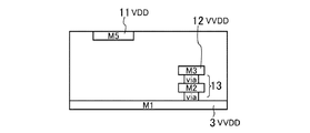
図1は第1実施形態に係る半導体集積回路装置の構成を示す平面図であり、電源遮断を行う回路ブロックにおけるレイアウトパターンを簡略化して図示している(以降の平面図も同様)。図1に示す半導体集積回路装置は、基板に、複数のスタンダードセル1が配置されている。X方向(図面横方向、第1方向に相当)に並べて配置された複数のスタンダードセル1を備えたスタンダードセル列2が、Y方向(図面縦方向、第1方向と垂直をなす方向である第2方向)に複数行配置されている。スタンダードセル1は、例えばインバータや論理回路等の機能を有する基本回路素子であり、スタンダードセル1を組み合わせて配置配線することによって、所定の機能を実現する半導体集積回路装置を設計・製造することができる。スタンダードセル1は、P型MOS(Metal Oxide Semiconductor)トランジスタ(PMOS)が形成されるN型領域とN型MOSトランジスタ(NMOS)が形成されるP型領域とをそれぞれ有している。本開示では、スタンダードセル1は、N型領域とP型領域とがY方向に並べて配置されており、かつ、スタンダードセル列2は、1行おきに、N型領域とP型領域との並びが反転しているものとする。なお、スタンダードセル1の内部構造については図示を省略している。(First Embodiment)
FIG. 1 is a plan view showing the configuration of the semiconductor integrated circuit device according to the first embodiment, and shows a simplified layout pattern in a circuit block for shutting off the power supply (the same applies to the subsequent plan views). In the semiconductor integrated circuit device shown in FIG. 1, a plurality of
スタンダードセル列2同士の間に、スタンダードセル1に電源電位を供給するスタンダードセル電源配線3(右横にVVDDと記す)と、スタンダードセル1に接地電位を供給する接地電源配線4(右横にVSSと記す)とが、交互に、配置されている。スタンダードセル電源配線3および接地電源配線4はともに、X方向に延びるように配置されている。スタンダードセル電源配線3は、そのY方向両側のスタンダードセル列2に電源電位を供給する。また接地電源配線4は、そのY方向両側のスタンダードセル列2に接地電位を供給する。そして、各スタンダードセル電源配線3に対して、スイッチセル20(ハッチを付している)が設けられている。スイッチセル20は、スタンダードセル1に対する電源供給を遮断するか否かを制御するものであり、制御信号に応じて、スタンダードセル電源配線3と、後述するストラップ電源配線11とを電気的に接続するか否かを切替可能に構成されている。制御信号は例えば、電源遮断を制御する制御ブロックから送られる。
Between the
図2はスイッチセル20の構成例を示す模式図である。なお図2では、構成を回路記号によって図示しているが、実際には、拡散領域やゲート配線、メタル配線等からなるレイアウトが形成される。図2に示すスイッチセル20は、ダブルハイトセルであり、ストラップ電源配線11と接続される入力端子21と、制御信号を受ける制御端子22と、PMOS23と、制御端子22に与えられた制御信号を受けるバッファ24とを備えている。PMOS23は、ソースが入力端子21と接続され、ドレインがスタンダードセル電源配線3と接続され、ゲートにバッファ24の出力を受ける。制御信号がハイレベルのとき、PMOS23は導通せず、入力端子21とスタンダードセル電源配線3とは電気的に遮断される。一方、制御信号がローレベルのとき、PMOS23は導通し、入力端子21とスタンダードセル電源配線3とは電気的に接続される。なお、図2では図示を省略しているが、バッファ24には入力端子21を介して電源が供給される。
FIG. 2 is a schematic view showing a configuration example of the
図1に戻り、スタンダードセル列2やスタンダードセル電源配線3の上層に、Y方向に延びるように配置されたストラップ電源配線11が設けられている。ストラップ電源配線11は、その下方に配置されているスイッチセル20の入力端子21と接続されている。また、スタンダードセル列2やスタンダードセル電源配線3の上層に、Y方向に延びるように配置された副ストラップ電源配線12が設けられている。副ストラップ電源配線12は、ビア構造13を介して、その下方を通過するスタンダードセル電源配線3と接続されている。図1の構成では、ストラップ電源配線11は、平面視において、スイッチセル20と重なりを有している。また、副ストラップ電源配線12も、平面視において、スイッチセル20と重なりを有している。なお本願明細書では、「ストラップ電源配線」は、スタンダードセル列2の方向と直交する方向に延びる電源配線という意味で用いている。また、図1では図示を省略しているが、接地電位を供給するためのストラップ電源配線も、スタンダードセル列2やスタンダードセル電源配線3の上層に、図面縦方向に延びるように配置されている。
Returning to FIG. 1, a strap
なお、図1では、電源供給元からスイッチセル20までの電源配線、すなわちストラップ電源配線11には「VDD」と記しており、スイッチセル20を経由した後の電源配線、すなわち副ストラップ電源配線12およびスタンダードセル電源配線3には「VVDD」と記している。以降の図でも同様である、ただし、スイッチセル20におけるPMOS23の導通時に供給される電源電位は、「VDD」と記された電源配線と「VVDD」と記された電源配線とで共通である。
In FIG. 1, the power supply wiring from the power supply source to the
図3は図1のIII−III断面図、図4は図1のIV−IV断面図であり、いずれもスイッチセル20が配置された箇所における断面構造を示している。図1の半導体集積回路装置は、基板上に5層以上の配線層を有している。図3および図4に示すように、基板側から順に積層するように、第1〜第5配線層(M1〜M5)が形成されている。ストラップ電源配線11は第5配線層(M5)に形成されており、副ストラップ電源配線12は第3配線層(M3)に形成されている。すなわち、ここでは、副ストラップ電源配線12は、ストラップ電源配線11よりも下層に設けられている。またスタンダードセル電源配線3は、第1配線層(M1)に形成されている。また図示はしていないが、接地電源配線4は第1配線層に形成されており、スタンダードセル1の信号配線は主に第1配線層に形成されている。なお図1において、第1、第2および第4配線層の優先配線方向はX方向であり、第3および第5配線層の優先配線方向はY方向である。
FIG. 3 is a sectional view taken along line III-III of FIG. 1, and FIG. 4 is a sectional view taken along line IV-IV of FIG. 1, both of which show a cross-sectional structure at a location where the
ここで、図1の構成におけるスイッチセル20の配置位置について、説明する。スイッチセル20は、ストラップ電源配線11とスタンダードセル電源配線3とが平面視で交差する箇所において、当該ストラップ電源配線11と当該スタンダードセル電源配線3との間に、設けられている。ただし、ストラップ電源配線11とスタンダードセル電源配線3とが平面視で交差する箇所であっても、スイッチセル20が配置されていない箇所がある。
Here, the arrangement position of the
図1の構成では、各ストラップ電源配線11について、スイッチセル20は、スタンダードセル電源配線3の4本毎に配置されている。言い換えると、各ストラップ電源配線11について、Y方向において隣り合うスイッチセル20同士の間には、3本のスタンダードセル電源配線3が存在する。そして、スイッチセル20のY方向における配置位置は、隣り合うストラップ電源配線11において互いに異なっている。また、スイッチセル20のY方向における配置位置は、ストラップ電源配線11の4本毎に、同一になっている。
In the configuration of FIG. 1, for each strap
例えば、図面下側の4本のスタンダードセル電源配線3((1)〜(4)を付している)と、図面左側の4本のストラップ電源配線11((1)〜(4)を付している)とに着目する。ストラップ電源配線11(1)は、スタンダードセル電源配線3(1)との間にのみスイッチセル20が配置されており、他のスタンダードセル電源配線3(2)〜(4)との間にはスイッチセル20は配置されていない。同様に、ストラップ電源配線11(2)は、スタンダードセル電源配線3(3)との間にのみスイッチセル20が配置されており、ストラップ電源配線11(3)は、スタンダードセル電源配線3(2)との間にのみスイッチセル20が配置されており、ストラップ電源配線11(4)は、スタンダードセル電源配線3(4)との間にのみスイッチセル20が配置されている。すなわち、4本のストラップ電源配線11(1)〜(4)について、スタンダードセル電源配線3(1),(3),(2),(4)の順で、その間にスイッチセル20が配置されている。そして、このようなスイッチセル20の配置が、X方向およびY方向において繰り返されている。
For example, the four standard cell power supply wirings 3 (with (1) to (4)) on the lower side of the drawing and the four strap power supply wirings 11 ((1) to (4)) on the left side of the drawing are attached. ) And pay attention to. In the strap power supply wiring 11 (1), the
ここで、スタンダードセル1A(ハッチを付している)に着目する。図1では、スタンダードセル1Aに対する電源供給経路の一部に矢印付き破線を付している。スタンダードセル1Aは、スタンダードセル電源配線3(2)に接続されるが、スタンダードセル電源配線3(2)に設けられたスイッチセル201,202からは離れている。このため、電源電圧降下が懸念される。この一方で、スタンダードセル電源配線3(2)に隣りあうスタンダードセル電源配線3(1)には、スタンダードセル1Aに近接した位置に、スイッチセル203が配置されている。このため、スタンダードセル1Aは、スイッチセル203から副ストラップ電源配線12を介して電源が供給されるので、電源電圧降下が抑制される。すなわち、第1スイッチセルとしてのスイッチセル201と第2スイッチセルとしてのスイッチセル202は、スタンダードセル電源配線3(2)に対してそれぞれ設けられており、X方向において隣り合っている。第3スイッチセルとしてのスイッチセル203は、スタンダードセル電源配線3(2)とY方向において隣りあうスタンダードセル電源配線3(1)に設けられている。そして、スイッチセル203は、スイッチセル201が設けられたストラップ電源配線11とスイッチセル202が設けられたストラップ電源配線11との間の中間位置にある、ストラップ電源配線11に対して、設けられている。
Here, focus on the
このように、図1の構成では、スタンダードセル1は、自己が接続されたスタンダードセル電源配線3に設けられたスイッチセル20から離れている場合でも、隣り合うスタンダードセル電源配線3に設けられたスイッチセル20が、その近傍に配置されている。例えば、X方向において隣り合うスイッチセル20同士の間の中間位置にあるスタンダードセル1に、Y方向において隣り合う位置に、スイッチセル20が配置されている。このため、そのスイッチセル20から副ストラップ電源配線12を介した電源供給がなされるので、電源電圧降下が抑制される。したがって、本実施形態によると、スイッチセル20の個数を少なく抑えつつ、各スタンダードセル1における電源電圧降下を抑制することができる。
As described above, in the configuration of FIG. 1, the
なお、図1の構成では、副ストラップ電源配線12は、ストラップ電源配線11の隣りにそれぞれ並べて配置しているが、これに限られるものではない。例えば、副ストラップ電源配線12を、ストラップ電源配線11から間隔を空けて配置し、スイッチセル20と平面視で重ならないようにしてもかまわない。また、一部のストラップ電源配線11には、副ストラップ電源配線12を隣りに並べないようにしてもよい。
In the configuration of FIG. 1, the sub-strap
また、図1の構成では、スイッチセル20は、ストラップ電源配線11の下方に配置されており、ストラップ電源配線11は平面視においてスイッチセル20と重なりを有しているものとしたが、これに限られるものではない。ただし、スイッチセル20をストラップ電源配線11の下方に配置した場合、スイッチセル20の入力端子21とストラップ電源配線11との間の配線やビア等の経路における抵抗値が小さくなるため、電源電圧の電圧降下が抑制される。また、図1の構成では、副ストラップ電源配線12は平面視においてスイッチセル20と重なりを有しているものとしたが、これに限られるものではない。
Further, in the configuration of FIG. 1, the
また、図1の構成では、副ストラップ電源配線12は、下方を通過する全てのスタンダードセル電源配線3と電気的に接続しているが、これに限られるものではない。例えば、下方を通過するスタンダードセル電源配線3の一部のみと電気的に接続するものとしてもよい。
Further, in the configuration of FIG. 1, the sub-strap
(変形例1)
図1の構成では、4本のストラップ電源配線11(1)〜(4)について、スタンダードセル電源配線3(1),(3),(2),(4)の順で、その間にスイッチセル20が配置されているものとした。ただし、スイッチセル20の配置パターンは、図1に示したものに限られるものではない。(Modification example 1)
In the configuration of FIG. 1, for the four strap power supply wirings 11 (1) to (4), the standard cell power supply wirings 3 (1), (3), (2), and (4) are arranged in this order, and the switch cells are in between. It is assumed that 20 is arranged. However, the arrangement pattern of the
図5は本実施形態の変形例1に係る半導体集積回路装置の構成を示す平面図である。スタンダードセル1の配置や、スタンダードセル電源配線3、接地電源配線4、ストラップ電源配線11および副ストラップ電源配線12の配置に関しては、図1と同様であり、ここではその詳細な説明を省略する。
FIG. 5 is a plan view showing the configuration of the semiconductor integrated circuit device according to the first modification of the present embodiment. The arrangement of the
図5の構成では、図1の構成と同様に、各ストラップ電源配線11について、スイッチセル20は、スタンダードセル電源配線3の4本毎に配置されている。そして、スイッチセル20のY方向における配置位置は、隣り合うストラップ電源配線11において互いに異なっている。また、スイッチセル20のY方向における配置位置は、ストラップ電源配線11の4本毎に、同一になっている。
In the configuration of FIG. 5, similarly to the configuration of FIG. 1, for each strap
ただし、図5の構成では、スイッチセル20の配置パターンが、図1の構成と異なっている。すなわち、ストラップ電源配線11(1)は、スタンダードセル電源配線3(1)との間にのみスイッチセル20が配置されており、他のスタンダードセル電源配線3(2)〜(4)との間にはスイッチセル20は配置されていない。同様に、ストラップ電源配線11(2)は、スタンダードセル電源配線3(2)との間にのみスイッチセル20が配置されており、ストラップ電源配線11(3)は、スタンダードセル電源配線3(3)との間にのみスイッチセル20が配置されており、ストラップ電源配線11(4)は、スタンダードセル電源配線3(4)との間にのみスイッチセル20が配置されている。すなわち、4本のストラップ電源配線11(1)〜(4)について、スタンダードセル電源配線3(1),(2),(3),(4)の順に、その間にスイッチセル20が配置されている。そして、このようなスイッチセル20の配置が、X方向およびY方向において繰り返されている。
However, in the configuration of FIG. 5, the arrangement pattern of the
図5の構成においても、スタンダードセル1は、自己が接続されたスタンダードセル電源配線3に設けられたスイッチセル20から離れている場合でも、隣り合うスタンダードセル電源配線3に設けられたスイッチセル20が、その近傍に配置されている。このため、そのスイッチセル20から副ストラップ電源配線12を介した電源供給がなされるので、電源電圧降下が抑制される。したがって、スイッチセル20の個数を少なく抑えつつ、各スタンダードセル1における電源電圧降下を抑制することができる。
Also in the configuration of FIG. 5, the
(変形例2)
図6は本実施形態の変形例2に係る半導体集積回路装置の構成を示す平面図である。図6では、図の簡略化のために、スタンダードセル1の配置に関しては図示を省略している。また、スタンダードセル電源配線3、接地電源配線4、ストラップ電源配線11および副ストラップ電源配線12の配置に関しては、図1とほぼ同様であり、ここではその詳細な説明を省略する。(Modification 2)
FIG. 6 is a plan view showing the configuration of the semiconductor integrated circuit device according to the second modification of the present embodiment. In FIG. 6, for the sake of simplification of the figure, the arrangement of the
図6の構成では、スイッチセル25は、Y方向におけるサイズすなわちセル高さが図1のスイッチセル20の2倍になっており、スタンダードセル列2の4列分のセル高さを有している。そして、各スイッチセル25は、ストラップ電源配線11と2本のスタンダードセル電源配線3との間に設けられている。すなわち、2本のスタンダードセル電源配線3を1個の「配線組」として捉えたとき、各スイッチセル25は、ストラップ電源配線11と配線組との間に設けられている。
In the configuration of FIG. 6, the size of the switch cell 25 in the Y direction, that is, the cell height is twice that of the
そして図6の構成では、各ストラップ電源配線11について、スイッチセル25は、4個の配線組毎に配置されている。そして、スイッチセル25のY方向における配置位置は、隣り合うストラップ電源配線11において互いに異なっている。また、スイッチセル25のY方向における配置位置は、ストラップ電源配線11の4本毎に、同一になっている。
In the configuration of FIG. 6, the switch cells 25 are arranged for each of the four wiring sets for each strap
例えば、図面左側の4本のストラップ電源配線11((1)〜(4)を付している)と、図面下側の4個の配線組(1)〜(4)に着目する。ストラップ電源配線11(1)は、配線組(1)との間にのみスイッチセル25が配置されており、他の配線組(2)〜(4)との間にはスイッチセル25は配置されていない。同様に、ストラップ電源配線11(2)は、配線組(3)との間にのみスイッチセル25が配置されており、ストラップ電源配線11(3)は、配線組(2)との間にのみスイッチセル25が配置されており、ストラップ電源配線11(4)は、配線組(4)との間にのみスイッチセル25が配置されている。すなわち、4本のストラップ電源配線11(1)〜(4)について、配線組(1),(3),(2),(4)の順に、その間にスイッチセル25が配置されている。そして、このようなスイッチセル25の配置が、X方向およびY方向において繰り返されている。 For example, pay attention to the four strap power supply wirings 11 (attached (1) to (4)) on the left side of the drawing and the four wiring sets (1) to (4) on the lower side of the drawing. In the strap power supply wiring 11 (1), the switch cell 25 is arranged only between the wiring set (1) and the other wiring sets (2) to (4). Not done. Similarly, the strap power supply wiring 11 (2) has the switch cell 25 arranged only between the wiring set (3) and the strap power supply wiring 11 (3) only between the strap power supply wiring 11 (3) and the wiring set (2). The switch cell 25 is arranged, and the strap power supply wiring 11 (4) is arranged only between the switch cell 25 and the wiring set (4). That is, the switch cells 25 are arranged between the four strap power supply wirings 11 (1) to (4) in the order of the wiring sets (1), (3), (2), and (4). Then, such arrangement of the switch cell 25 is repeated in the X direction and the Y direction.
すなわち、図6の構成では、図1のスイッチセル20と同様の配置パターンに従って、スイッチセル25が配置されている。したがって、スイッチセル25の個数を少なく抑えつつ、各スタンダードセル1における電源電圧降下を抑制することができる。
That is, in the configuration of FIG. 6, the switch cells 25 are arranged according to the same arrangement pattern as the
なお、スイッチセル25の配置パターンは、図1に示したものに限られるものではない。例えば図5の構成と同様に、4本のストラップ電源配線11(1)〜(4)について、配線組(1),(2),(3),(4)の順に、その間にスイッチセル25が配置されるようにしてもよい。 The arrangement pattern of the switch cell 25 is not limited to that shown in FIG. For example, as in the configuration of FIG. 5, for the four strap power supply wirings 11 (1) to (4), the wiring set (1), (2), (3), and (4) are arranged in this order, and the switch cell 25 is in between. May be arranged.
(変形例3)
図7は本実施形態の変形例3に係る半導体集積回路装置の構成を示す平面図である。図7では、図の簡略化のために、スタンダードセル1の配置に関しては図示を省略している。また、スタンダードセル電源配線3、接地電源配線4、ストラップ電源配線11および副ストラップ電源配線12の配置に関しては、図1とほぼ同様であり、ここではその詳細な説明を省略する。(Modification example 3)
FIG. 7 is a plan view showing the configuration of the semiconductor integrated circuit device according to the third modification of the present embodiment. In FIG. 7, for the sake of simplification of the figure, the arrangement of the
図7の構成では、スイッチセル26は、Y方向におけるサイズすなわちセル高さが図1のスイッチセル20の3倍になっており、スタンダードセル列2の6列分のセル高さを有している。そして、各スイッチセル26は、ストラップ電源配線11と3本のスタンダードセル電源配線3との間に設けられている。すなわち、3本のスタンダードセル電源配線3を1個の「配線組」として捉えたとき、各スイッチセル26は、ストラップ電源配線11と配線組との間に設けられている。
In the configuration of FIG. 7, the size of the
そして図7の構成では、図6の構成と同様に、各ストラップ電源配線11について、スイッチセル26は、4個の配線組毎に配置されている。そして、スイッチセル26のY方向における配置位置は、隣り合うストラップ電源配線11において互いに異なっている。また、スイッチセル26のY方向における配置位置は、ストラップ電源配線11の4本毎に、同一になっている。
In the configuration of FIG. 7, the
例えば、図面左側の4本のストラップ電源配線11((1)〜(4)を付している)と、図面下側の4個の配線組(1)〜(4)に着目する。ストラップ電源配線11(1)は、配線組(1)との間にのみスイッチセル26が配置されており、他の配線組(2)〜(4)との間にはスイッチセル26は配置されていない。同様に、ストラップ電源配線11(2)は、配線組(3)との間にのみスイッチセル26が配置されており、ストラップ電源配線11(3)は、配線組(2)との間にのみスイッチセル26が配置されており、ストラップ電源配線11(4)は、配線組(4)との間にのみスイッチセル26が配置されている。すなわち、4本のストラップ電源配線11(1)〜(4)について、配線組(1),(3),(2),(4)の順に、その間にスイッチセル26が配置されている。そして、このようなスイッチセル26の配置が、X方向およびY方向において繰り返されている。
For example, pay attention to the four strap power supply wirings 11 (attached (1) to (4)) on the left side of the drawing and the four wiring sets (1) to (4) on the lower side of the drawing. In the strap power supply wiring 11 (1), the
すなわち、図7の構成は、図1の構成と同様の配置パターンに従って、スイッチセル26が配置されている。したがって、スイッチセル26の個数を少なく抑えつつ、各スタンダードセル1における電源電圧降下を抑制することができる。
That is, in the configuration of FIG. 7, the
なお、スイッチセル26の配置パターンは、図7に示したものに限られるものではない。例えば図5の構成と同様に、4本のストラップ電源配線11(1)〜(4)について、配線組(1),(2),(3),(4)の順に、その間にスイッチセル26が配置されていてもよい。
The arrangement pattern of the
ここで、変形例2では、2本のスタンダードセル電源配線3を1個の「配線組」として捉えるものとし、変形例3では、3本のスタンダードセル電源配線3を1個の「配線組」として捉えるものとしたが、配線組に属するスタンダードセル電源配線3の本数は、2本または3本に限られるものではない。例えば、4本のスタンダードセル電源配線3を1個の「配線組」として捉えて、スタンダードセル列2の8列分のセル高さを有するスイッチセルを、本実施形態と同様に配置してもよい。また、図1や図5の構成は、1本のスタンダードセル電源配線3を1個の「配線組」として捉えたものに相当する。すなわち、N本(Nは1以上の整数)のスタンダードセル電源配線3を1個の配線組として捉えて、スイッチセルを配置すればよい。
Here, in the modified example 2, the two standard cell
(第2実施形態)
図8は第2実施形態に係る半導体集積回路装置の構成を示す平面図である。スタンダードセル1の配置や、スタンダードセル電源配線3、接地電源配線4、ストラップ電源配線11および副ストラップ電源配線12の配置に関しては、図1と同様であり、ここではその詳細な説明を省略する。(Second Embodiment)
FIG. 8 is a plan view showing the configuration of the semiconductor integrated circuit device according to the second embodiment. The arrangement of the
図8では、図1と対比すると、ストラップ電源配線11および副ストラップ電源配線12の上層に、X方向に延びる上層電源配線14が配置されている。上層電源配線14は、その下層にある副ストラップ電源配線12とビア16によって接続されている。このように、副ストラップ電源配線12同士を接続する上層電源配線14を設けることによって、電源供給の強化ができるので、電源電圧降下をより抑制することが可能になる。
In FIG. 8, in comparison with FIG. 1, the upper layer
なお、図8の構成では、上層電源配線14は、下方を通過する全ての副ストラップ電源配線12と電気的に接続されているが、これに限られるものではない。例えば、上層電源配線14は、下方を通過する副ストラップ電源配線12の一部のみと電気的に接続するものとしてもよい。
In the configuration of FIG. 8, the upper layer
(第3実施形態)
図9は第3実施形態に係る半導体集積回路装置の構成を示す平面図である。スタンダードセル1の配置や、スタンダードセル電源配線3、接地電源配線4およびストラップ電源配線11の配置に関しては、図1と同様であり、ここではその詳細な説明を省略する。(Third Embodiment)
FIG. 9 is a plan view showing the configuration of the semiconductor integrated circuit device according to the third embodiment. The arrangement of the
図9では、図1と対比すると、副ストラップ電源配線の本数が増えている。例えば、領域A1,A2では、ストラップ電源配線11同士の間に、副ストラップ電源配線12が2本配置されている。また、領域A3では、ストラップ電源配線11同士の間に、副ストラップ電源配線12に加えて、副ストラップ電源配線12とは異なる配線層(ここでは第5配線層(M5)とする)に形成された副ストラップ電源配線15が配置されている。なお、ストラップ電源配線11同士の間に、副ストラップ電源配線12,15を3本以上配置してもかまわない。
In FIG. 9, the number of sub-strap power supply wirings is increased as compared with FIG. For example, in the areas A1 and A2, two sub-strap
このように、副ストラップ電源配線12,15の本数を増やすことによって、スイッチセル20の個数を増やすことなく、電源供給の強化ができるので、半導体集積回路装置の面積増加を抑制することができる。
By increasing the number of the sub-strap
(第4実施形態)
図10は第4実施形態に係る半導体集積回路装置の構成を示す平面図である。スタンダードセル1の配置や、スタンダードセル電源配線3、接地電源配線4、ストラップ電源配線11および副ストラップ電源配線12の配置に関しては、図1とほぼ同様であり、ここではその詳細な説明を省略する。(Fourth Embodiment)
FIG. 10 is a plan view showing the configuration of the semiconductor integrated circuit device according to the fourth embodiment. The arrangement of the
図10の構成では、標準の駆動能力を有するスイッチセル20aと、高い駆動能力を有するスイッチセル20bとが配置されている。スイッチセル20aとスイッチセル20bとは、トランジスタサイズが互いに異なっている。ここで、破線で囲んだ領域Xは電源供給を強化したい領域である。ところが、領域Xにはスタンダードセル1が高密度で配置されているため、スイッチセル20aをこれ以上追加できない。そこで、領域Xの周囲に、スイッチセル20aよりも駆動能力が高いスイッチセル20bを配置している。これにより、領域X内に、駆動能力が高いスイッチセル20bから副ストラップ電源配線12を介して、電源を供給することができる。
In the configuration of FIG. 10, a
(スイッチセルの配置パターンおよび配置手法)
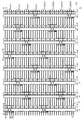
図11は図1の構成におけるスイッチセル20の配置パターンを概念的に示す図である。図11では、X軸方向に延びる各行がスタンダードセル電源配線3に対応し、Y軸方向に延びる各列がストラップ電源配線11に対応している。そして、各マスはそれぞれ、スタンダードセル電源配線3とストラップ電源配線11とが平面視で交差した箇所、言い換えると、スイッチセル20が配置される可能性がある箇所に対応している。そして、灰色のマスはスイッチセル20が配置された箇所を表しており、白いマスはスイッチセル20が配置されていない箇所を表している。なお、図6や図7の構成のように、スイッチセル20よりもセル高さが高いスイッチセル25,26が、複数のスタンダードセル電源配線3に対して配置されている場合は、図11のX軸方向に延びる各行は、複数のスタンダードセル電源配線3からなる「配線組」に対応することになる。(Switch cell placement pattern and placement method)
FIG. 11 is a diagram conceptually showing an arrangement pattern of the
図11において、白いマスには、当該マスに最も近い灰色のマスまでの距離を表す数字が記されている。具体的には、当該マスと灰色のマスとの間の、X座標の差およびY座標の差を加えた値の、最小値を記している。図11では、白いマスは、全て「1」が記されている。すなわち、スイッチセルが配置されていない箇所はいずれも、その上下左右のいずれかにスイッチセルが配置されている。 In FIG. 11, the white square is marked with a number indicating the distance to the gray square closest to the square. Specifically, the minimum value of the value obtained by adding the difference in the X coordinate and the difference in the Y coordinate between the square and the gray square is described. In FIG. 11, all white squares are marked with "1". That is, the switch cells are arranged on either the top, bottom, left, or right of any of the places where the switch cells are not arranged.
図12は対比例としてのスイッチセルの配置パターンを概念的に示す図である。図12では、スイッチセルはいわゆる千鳥状に配置されている。図12から分かるように、この千鳥状の配置パターンでも、白いマスは全て「1」が記されており、スイッチセルが配置されていない箇所はいずれも、その上下左右のいずれかにスイッチセルが配置されている。したがって、電源電圧降下の抑制効果は得られる。ただし、図11と対比すると分かるように、必要とするスイッチセルの個数が、上述の実施形態の2倍になっており、格段に多くなっている。すなわち、本実施形態では、スイッチセルの個数を少なく抑えつつ、各スタンダードセル1における電源電圧降下を抑制することができる。
FIG. 12 is a diagram conceptually showing an arrangement pattern of switch cells as a inverse proportion. In FIG. 12, the switch cells are arranged in a so-called staggered pattern. As can be seen from FIG. 12, even in this staggered arrangement pattern, all the white squares are marked with "1", and the switch cells are located on either the top, bottom, left, or right of the places where the switch cells are not arranged. Have been placed. Therefore, the effect of suppressing the power supply voltage drop can be obtained. However, as can be seen in comparison with FIG. 11, the number of required switch cells is twice that of the above-described embodiment, which is significantly larger. That is, in the present embodiment, it is possible to suppress the power supply voltage drop in each
なお、上述の実施形態では、4本のストラップ電源配線11と、4本のスタンダードセル電源配線3または4個の配線組とを1つの単位として、スイッチセル20,25,26の配置パターンが設定されていた。ただし、本開示はこれに限定されるものではない。すなわち、M(Mは3以上の整数)本のストラップ電源配線11と、M本のスタンダードセル電源配線3またはM個の配線組とを1つの単位として、スイッチセル20,25,26の配置パターンを設定すればよい。
In the above-described embodiment, the arrangement patterns of the
この場合、スイッチセルの配置パターンは、例えば次のように設定すればよい。図13を参照して、M=8の場合を例にとって、説明する。まず、M個×M個のマスからなるマス目を作成する。マス目において、X軸方向に延びる各行は、スタンダードセル電源配線3または複数のスタンダードセル電源配線3からなる配線組に対応し、Y軸方向に延びる各列は、ストラップ電源配線11に対応している。まず、左上の座標(1,1)を出発点とし、スイッチセルを配置する。その後、1マス下に下りてからmx(図13ではmx=3)段右に移動し、その座標にスイッチセルを配置する。この動作を繰り返し行う。この結果、図13に示すような配置パターンが得られる。
In this case, the arrangement pattern of the switch cells may be set as follows, for example. A case of M = 8 will be described as an example with reference to FIG. First, a square consisting of M × M squares is created. In the grid, each row extending in the X-axis direction corresponds to a wiring set consisting of the standard cell
図14および図15は上のような手法によって得られたスイッチセルの配置パターンである。図14において、(a)はM=3、(b)はM=5、(c)はM=6、(d)はM=7の場合であり、図15において、(a)はM=8、(b)はM=12、(c)はM=16の場合である。表現方法は図11と同一であり、灰色のマスは、スイッチセルが配置された箇所に対応しており、白いマスには、当該マスに最も近い灰色のマス(すなわち最も近いスイッチセル)までの距離を表す数字が記されている。 14 and 15 are switch cell arrangement patterns obtained by the above method. In FIG. 14, (a) is M = 3, (b) is M = 5, (c) is M = 6, and (d) is M = 7. In FIG. 15, (a) is M =. 8, (b) is the case of M = 12, and (c) is the case of M = 16. The expression method is the same as in FIG. 11, the gray cell corresponds to the place where the switch cell is arranged, and the white cell corresponds to the gray cell closest to the cell (that is, the nearest switch cell). A number representing the distance is written.
Mの値と、移動量mxの値との関係は次のとおりである。
M=3:mx=2
M=4:mx=2,3,2の順
M=5:mx=2
M=6:mx=2,3,4,4,3,2の順
M=7:mx=3
M=8:mx=3
M=12:mx=5
M=16:mx=5The relationship between the value of M and the value of the movement amount mx is as follows.
M = 3: mx = 2
M = 4: mx = 2,3,2 order M = 5: mx = 2
M = 6: mx = 2,3,4,4,3,2 order M = 7: mx = 3
M = 8: mx = 3
M = 12: mx = 5
M = 16: mx = 5
ここで、白いマスに記された数字の最大値をDmaxとすると、次のようになる。
M=3:Dmax=1
M=4:Dmax=1
M=5:Dmax=1
M=6:Dmax=2
M=7:Dmax=2
M=8:Dmax=2
M=12:Dmax=3
M=16:Dmax=4Here, assuming that the maximum value of the numbers written in the white cells is Dmax, the result is as follows.
M = 3: Dmax = 1
M = 4: Dmax = 1
M = 5: Dmax = 1
M = 6: Dmax = 2
M = 7: Dmax = 2
M = 8: Dmax = 2
M = 12: Dmax = 3
M = 16: Dmax = 4
この例では、M=4,5,8,12,16では、次の関係が成り立っている。
Dmax ≦ M/4In this example, when M = 4,5,8,12,16, the following relationship holds.
Dmax ≤ M / 4
図14および図15に示すスイッチセルの配置パターンを半導体集積回路装置に適用することによって、電源電圧降下を、少ない個数のスイッチセルによって、より効果的に抑制することができる。 By applying the switch cell arrangement pattern shown in FIGS. 14 and 15 to the semiconductor integrated circuit device, the power supply voltage drop can be more effectively suppressed by a small number of switch cells.
(その他の実施形態)
上の説明では、ストラップ電源配線11は第5配線層に設けられ、副ストラップ電源配線12,15は第3配線層および第5配線層に設けられるものとしたが、ストラップ電源配線や副ストラップ電源配線が形成される配線層はこれらに限られるものではない。ただし、副ストラップ電源配線は、スタンダードセル電源配線にできるだけ近い配線層に形成することが好ましい。これにより、副ストラップ電源配線とスタンダードセル電源配線との間の配線やビア等の経路における抵抗値が小さくなり、電源電位の低下を抑制することができる。また、上の説明では、スタンダードセル電源配線3は第1配線層に設けられるものとしたが、これに限られるものではなく、例えば複数の配線層に設けてもかまわない。(Other embodiments)
In the above description, the strap
また、図2に示したスイッチセル20の構成はあくまでも一例であり、スイッチセル20は、制御信号に応じて、スタンダードセル電源配線3とストラップ電源配線11とを電気的に接続するか否かを切替可能に構成されていればよい。例えば図2において、バッファ24に代えてインバータを用いてもよい。この場合は、制御信号の論理と接続/遮断との関係が上で説明したものと逆になる。あるいは、図2に示した回路構成を2組設けてもかまわない。また、図2の構成例では、スイッチセル20はダブルハイトセルとしたが、シングルハイトセルとしてもよい。
Further, the configuration of the
また、上の説明では、電源電位を供給するスタンダードセル電源配線3に対してスイッチセル20を設けるものとしたが、これに代えて、接地電位を供給する接地電源配線4にスイッチセルを設けて、上で説明したものと同様の構成を適用してもよい。この場合は,副ストラップ電源配線は、接地電源配線4を接続するように設ければよい。
Further, in the above description, the
本開示では、電源遮断技術を用いた半導体集積回路装置について、スイッチセルを増やすことなく、電源供給の強化が可能になるので、例えば、LSIの消費電力削減や面積削減に有効である。 In the present disclosure, it is possible to strengthen the power supply of the semiconductor integrated circuit device using the power cutoff technology without increasing the number of switch cells, which is effective for reducing the power consumption and the area of the LSI, for example.
1 スタンダードセル
2 スタンダードセル列
3 スタンダードセル電源配線(電源配線)
11 ストラップ電源配線
12,15 副ストラップ電源配線
14 上層電源配線
20,20a,20b スイッチセル
25,26 スイッチセル
201 第1スイッチセル
202 第2スイッチセル
203 第3スイッチセル1
11 Strap
Claims (12)
前記第1方向に延びるようにそれぞれ配置されており、前記複数のスタンダードセルに電源を供給する複数の電源配線と、
前記複数の電源配線の上層において前記第2方向に延びるように配置された、複数のストラップ電源配線と、
前記複数の電源配線の上層において前記第2方向に延びるように配置され、前記複数の電源配線とそれぞれ接続された、複数の副ストラップ電源配線と、
前記複数のストラップ電源配線のいずれかと、前記複数の電源配線の中のN本(Nは1以上の整数)からなる配線組との間に設けられており、制御信号に応じて、当該ストラップ電源配線と当該配線組に属する前記電源配線とを電気的に接続するか否かを切替可能に構成された、複数のスイッチセルとを備え、
前記複数のスイッチセルは、前記複数のストラップ電源配線に対してそれぞれ、M(Mは3以上の整数)個の前記配線組毎に1個ずつ、配置されており、
前記複数のスイッチセルの前記第2方向における配置位置は、隣り合う前記ストラップ電源配線において互いに異なっており、かつ、前記第1方向における前記ストラップ電源配線のM本ごとに、同一である
ことを特徴とする半導体集積回路装置。 A plurality of standard cell rows arranged side by side in the first direction are provided, and a plurality of standard cell rows arranged side by side in the second direction, which is a direction perpendicular to the first direction, and a plurality of standard cell rows.
A plurality of power supply wirings that are arranged so as to extend in the first direction and supply power to the plurality of standard cells, and a plurality of power supply wirings.
A plurality of strap power supply wirings arranged so as to extend in the second direction in the upper layer of the plurality of power supply wirings,
A plurality of sub-strap power supply wirings arranged so as to extend in the second direction in the upper layer of the plurality of power supply wirings and connected to the plurality of power supply wirings, respectively.
It is provided between one of the plurality of strap power supply wirings and a wiring set consisting of N wires (N is an integer of 1 or more) in the plurality of power supply wirings, and the strap power supply is provided according to a control signal. It is provided with a plurality of switch cells configured to be able to switch whether or not to electrically connect the wiring and the power supply wiring belonging to the wiring set.
The plurality of switch cells are arranged one by one for each of the M (M is an integer of 3 or more) wiring sets for the plurality of strap power supply wirings.
The arrangement positions of the plurality of switch cells in the second direction are different from each other in the adjacent strap power supply wirings, and are the same for each M of the strap power supply wirings in the first direction. Semiconductor integrated circuit device.
前記複数の副ストラップ電源配線の上層に、前記第1方向に延びるように配置されており、前記複数の副ストラップ電源配線とそれぞれ接続された、上層電源配線を備えた
ことを特徴とする半導体集積回路装置。 In the semiconductor integrated circuit device according to claim 1,
A semiconductor integrated device is provided on an upper layer of the plurality of sub-strap power supply wirings so as to extend in the first direction and is provided with an upper layer power supply wiring connected to each of the plurality of sub-strap power supply wirings. Circuit equipment.
前記副ストラップ電源配線は、前記ストラップ電源配線よりも下層に設けられている
ことを特徴とする半導体集積回路装置。 In the semiconductor integrated circuit device according to claim 1,
The semiconductor integrated circuit device is characterized in that the sub-strap power supply wiring is provided in a lower layer than the strap power supply wiring.
前記ストラップ電源配線は、平面視において、前記スイッチセルと重なりを有している
ことを特徴とする半導体集積回路装置。 In the semiconductor integrated circuit device according to claim 1,
A semiconductor integrated circuit device characterized in that the strap power supply wiring has an overlap with the switch cell in a plan view.
前記副ストラップ電源配線は、平面視において、前記スイッチセルと重なりを有している
ことを特徴とする半導体集積回路装置。 In the semiconductor integrated circuit device according to claim 1,
A semiconductor integrated circuit device characterized in that the sub-strap power supply wiring has an overlap with the switch cell in a plan view.
前記複数のストラップ電源配線は、間に前記副ストラップ電源配線が2本以上配置された、2本のストラップ電源配線を含む
ことを特徴とする半導体集積回路装置。 In the semiconductor integrated circuit device according to claim 1,
Wherein the plurality of strap power supply lines, the auxiliary strap power supply wiring is disposed over two between, the semiconductor integrated circuit device which comprises two straps power wiring.
前記複数の副ストラップ電源配線は、配置された層が互いに異なる、2本の副ストラップ電源配線を含む
ことを特徴とする半導体集積回路装置。 In the semiconductor integrated circuit device according to claim 1,
The semiconductor integrated circuit device, wherein the plurality of sub-strap power supply wirings include two sub-strap power supply wirings in which arranged layers are different from each other.
前記スイッチセルは、トランジスタサイズが互いに異なる、2個のスイッチセルを含む
ことを特徴とする半導体集積回路装置。 In the semiconductor integrated circuit device according to claim 1,
The switch cell is a semiconductor integrated circuit device including two switch cells having different transistor sizes.
前記第1方向に延びるようにそれぞれ配置されており、前記複数のスタンダードセルに電源を供給する複数の電源配線と、
前記複数の電源配線の上層において前記第2方向に延びるように配置された、複数のストラップ電源配線と、
前記複数の電源配線の上層において前記第2方向に延びるように配置され、前記複数の電源配線とそれぞれ接続された、複数の副ストラップ電源配線と、
前記複数のストラップ電源配線のいずれかと、前記複数の電源配線の中のN本(Nは1以上の整数)からなる配線組との間に設けられており、制御信号に応じて、当該ストラップ電源配線と当該配線組に属する前記電源配線とを電気的に接続するか否かを切替可能に構成された、複数のスイッチセルとを備え、
前記複数のスイッチセルは、前記複数のストラップ電源配線に対してそれぞれ、M(Mは3以上の整数)個の前記配線組毎に1個ずつ、配置されており、
前記複数のスイッチセルの前記第2方向における配置位置は、隣り合う前記ストラップ電源配線において互いに異なっており、かつ、前記第1方向における前記ストラップ電源配線のM本ごとに、同一であり、
前記複数のスイッチセルは、前記配線組の1つである第1配線組に対してそれぞれ設けられており、前記第1方向において隣り合う第1および第2スイッチセルと、前記第1配線組と前記第2方向において隣り合う前記配線組に対して設けられた第3スイッチセルとを含み、
前記第3スイッチセルは、前記第1スイッチセルが設けられた前記ストラップ電源配線と前記第2スイッチセルが設けられた前記ストラップ電源配線と間の中間位置にある、前記ストラップ電源配線に対して、設けられている
ことを特徴とする半導体集積回路装置。 A plurality of standard cell rows arranged side by side in the first direction are provided, and a plurality of standard cell rows arranged side by side in the second direction, which is a direction perpendicular to the first direction, and a plurality of standard cell rows.
A plurality of power supply wirings that are arranged so as to extend in the first direction and supply power to the plurality of standard cells, and a plurality of power supply wirings.
A plurality of strap power supply wirings arranged so as to extend in the second direction in the upper layer of the plurality of power supply wirings,
A plurality of sub-strap power supply wirings arranged so as to extend in the second direction in the upper layer of the plurality of power supply wirings and connected to the plurality of power supply wirings, respectively.
It is provided between one of the plurality of strap power supply wirings and a wiring set consisting of N wires (N is an integer of 1 or more) in the plurality of power supply wirings, and the strap power supply is provided according to a control signal. It is provided with a plurality of switch cells configured to be able to switch whether or not to electrically connect the wiring and the power supply wiring belonging to the wiring set.
The plurality of switch cells are arranged one by one for each of the M (M is an integer of 3 or more) wiring sets for the plurality of strap power supply wirings.
The arrangement positions of the plurality of switch cells in the second direction are different from each other in the adjacent strap power supply wirings, and are the same for each M of the strap power supply wirings in the first direction.
The plurality of switch cells are provided for each of the first wiring set, which is one of the wiring sets, and the first and second switch cells adjacent to each other in the first direction, and the first wiring set. Including a third switch cell provided for the wiring set adjacent to each other in the second direction.
The third switch cell is located at an intermediate position between the strap power supply wiring provided with the first switch cell and the strap power supply wiring provided with the second switch cell, with respect to the strap power supply wiring. A semiconductor integrated circuit device characterized by being provided.
Mは4である
ことを特徴とする半導体集積回路装置。 In the semiconductor integrated circuit device according to claim 9,
A semiconductor integrated circuit device characterized in that M is 4.
前記第1方向に延びるようにそれぞれ配置されており、前記複数のスタンダードセルに電源を供給する複数の電源配線と、
前記複数の電源配線の上層において前記第2方向に延びるように配置された、複数のストラップ電源配線と、
前記複数の電源配線の上層において前記第2方向に延びるように配置され、前記複数の電源配線とそれぞれ接続された、複数の副ストラップ電源配線と、
前記複数のストラップ電源配線のいずれかと、前記複数の電源配線の中のN本(Nは1以上の整数)からなる配線組との間に設けられており、制御信号に応じて、当該ストラップ電源配線と当該配線組に属する前記電源配線とを電気的に接続するか否かを切替可能に構成された、複数のスイッチセルとを備え、
前記複数のスイッチセルは、前記複数のストラップ電源配線に対してそれぞれ、M(Mは3以上の整数)個の前記配線組毎に1個ずつ、配置されており、
前記複数のスイッチセルの前記第2方向における配置位置は、隣り合う前記ストラップ電源配線において互いに異なっており、かつ、前記第1方向における前記ストラップ電源配線のM本ごとに、同一であり、
前記複数のスイッチセルの配置を、X軸方向に延びる各行が前記配線組に対応し、Y軸方向に延びる各列が前記ストラップ電源配線に対応するマス目で表した場合において、
前記スイッチセルが配置されていない第1マスと、前記スイッチセルが配置されており当該第1マスから最も近い第2マスとの、X座標の差をX、Y座標の差をYとしたとき、
X+Y≦M/4
の関係を満たす
ことを特徴とする半導体集積回路装置。 A plurality of standard cell rows arranged side by side in the first direction are provided, and a plurality of standard cell rows arranged side by side in the second direction, which is a direction perpendicular to the first direction, and a plurality of standard cell rows.
A plurality of power supply wirings that are arranged so as to extend in the first direction and supply power to the plurality of standard cells, and a plurality of power supply wirings.
A plurality of strap power supply wirings arranged so as to extend in the second direction in the upper layer of the plurality of power supply wirings,
A plurality of sub-strap power supply wirings arranged so as to extend in the second direction in the upper layer of the plurality of power supply wirings and connected to the plurality of power supply wirings, respectively.
It is provided between one of the plurality of strap power supply wirings and a wiring set consisting of N wires (N is an integer of 1 or more) in the plurality of power supply wirings, and the strap power supply is provided according to a control signal. It is provided with a plurality of switch cells configured to be able to switch whether or not to electrically connect the wiring and the power supply wiring belonging to the wiring set.
The plurality of switch cells are arranged one by one for each of the M (M is an integer of 3 or more) wiring sets for the plurality of strap power supply wirings.
The arrangement positions of the plurality of switch cells in the second direction are different from each other in the adjacent strap power supply wirings, and are the same for each M of the strap power supply wirings in the first direction.
When the arrangement of the plurality of switch cells is represented by a grid in which each row extending in the X-axis direction corresponds to the wiring set and each column extending in the Y-axis direction corresponds to the strap power supply wiring.
When the difference in X coordinates between the first cell in which the switch cell is not arranged and the second cell in which the switch cell is arranged and is closest to the first cell is X and the difference in Y coordinates is Y. ,
X + Y ≤ M / 4
A semiconductor integrated circuit device characterized by satisfying the above relationship.
Mは4,8,12,16のうちのいずれかである
ことを特徴とする半導体集積回路装置。 In the semiconductor integrated circuit device according to claim 11.
A semiconductor integrated circuit device in which M is any of 4, 8, 12, and 16.
Applications Claiming Priority (5)
| Application Number | Priority Date | Filing Date | Title |
|---|---|---|---|
| JP2016110402 | 2016-06-01 | ||
| JP2016110402 | 2016-06-01 | ||
| JP2017077462 | 2017-04-10 | ||
| JP2017077462 | 2017-04-10 | ||
| PCT/JP2017/019015 WO2017208887A1 (en) | 2016-06-01 | 2017-05-22 | Semiconductor integrated circuit device |
Publications (2)
| Publication Number | Publication Date |
|---|---|
| JPWO2017208887A1 JPWO2017208887A1 (en) | 2019-03-28 |
| JP6898570B2 true JP6898570B2 (en) | 2021-07-07 |
Family
ID=60477489
Family Applications (1)
| Application Number | Title | Priority Date | Filing Date |
|---|---|---|---|
| JP2018520810A Active JP6898570B2 (en) | 2016-06-01 | 2017-05-22 | Semiconductor integrated circuit equipment |
Country Status (4)
| Country | Link |
|---|---|
| US (1) | US10734373B2 (en) |
| JP (1) | JP6898570B2 (en) |
| CN (1) | CN109155284B (en) |
| WO (1) | WO2017208887A1 (en) |
Families Citing this family (17)
| Publication number | Priority date | Publication date | Assignee | Title |
|---|---|---|---|---|
| DE102018108836B4 (en) | 2017-11-14 | 2023-10-05 | Taiwan Semiconductor Manufacturing Co. Ltd. | SEMICONDUCTOR DEVICES WITH STANDARD CELLS |
| US11011545B2 (en) * | 2017-11-14 | 2021-05-18 | Taiwan Semiconductor Manufacturing Co., Ltd. | Semiconductor device including standard cells |
| CN110531136B (en) * | 2018-05-23 | 2021-11-12 | 中芯国际集成电路制造(上海)有限公司 | Test circuit and test method for standard unit leakage current |
| US10784199B2 (en) * | 2019-02-20 | 2020-09-22 | Micron Technology, Inc. | Component inter-digitated VIAS and leads |
| JP7080845B2 (en) * | 2019-03-20 | 2022-06-06 | 株式会社東芝 | Semiconductor device |
| JP7259944B2 (en) | 2019-04-25 | 2023-04-18 | 株式会社ソシオネクスト | semiconductor equipment |
| WO2020217396A1 (en) | 2019-04-25 | 2020-10-29 | 株式会社ソシオネクスト | Semiconductor device |
| CN110752203B (en) * | 2019-10-30 | 2021-03-23 | 珠海格力电器股份有限公司 | A kind of low power consumption chip and preparation method thereof |
| US12136595B2 (en) | 2019-12-10 | 2024-11-05 | Samsung Electronics Co., Ltd. | Semiconductor device including power gating switches |
| CN113688594B (en) * | 2020-05-18 | 2024-06-21 | 元太科技工业股份有限公司 | Electronic Devices |
| CN116472605B (en) * | 2020-11-27 | 2025-06-24 | 株式会社索思未来 | Method for designing semiconductor integrated circuit device, and computer-readable recording medium |
| JP7600701B2 (en) | 2021-01-19 | 2024-12-17 | 株式会社ソシオネクスト | Semiconductor Device |
| JP7635557B2 (en) | 2021-01-19 | 2025-02-26 | 株式会社ソシオネクスト | Semiconductor Device |
| CN115472195A (en) * | 2021-07-27 | 2022-12-13 | 台湾积体电路制造股份有限公司 | Semiconductor device and method of operating the same |
| DE102022100096A1 (en) * | 2021-07-27 | 2023-02-02 | Taiwan Semiconductor Manufacturing Co., Ltd. | SEMICONDUCTOR DEVICE AND METHOD OF OPERATING THEREOF |
| CN113935273A (en) * | 2021-09-17 | 2022-01-14 | 东科半导体(安徽)股份有限公司 | Control signal connection method of low-power-consumption module |
| CN119949047A (en) * | 2022-09-27 | 2025-05-06 | 新唐科技日本株式会社 | Semiconductor integrated circuit device |
Family Cites Families (20)
| Publication number | Priority date | Publication date | Assignee | Title |
|---|---|---|---|---|
| JP3924471B2 (en) * | 2002-01-30 | 2007-06-06 | 株式会社リコー | Semiconductor integrated circuit including standard cell or macro cell, and placement and routing method thereof |
| JP4547939B2 (en) * | 2004-03-02 | 2010-09-22 | ソニー株式会社 | Semiconductor integrated circuit and layout design method thereof |
| US7279926B2 (en) * | 2004-05-27 | 2007-10-09 | Qualcomm Incoporated | Headswitch and footswitch circuitry for power management |
| US7659746B2 (en) * | 2005-02-14 | 2010-02-09 | Qualcomm, Incorporated | Distributed supply current switch circuits for enabling individual power domains |
| JP2007095787A (en) * | 2005-09-27 | 2007-04-12 | Nec Electronics Corp | Semiconductor integrated circuit |
| JP5307427B2 (en) | 2007-04-05 | 2013-10-02 | ルネサスエレクトロニクス株式会社 | Semiconductor device |
| JP5358913B2 (en) * | 2007-09-07 | 2013-12-04 | 日本電気株式会社 | Semiconductor integrated circuit and design method thereof |
| JP5528662B2 (en) | 2007-09-18 | 2014-06-25 | ソニー株式会社 | Semiconductor integrated circuit |
| JP4636077B2 (en) | 2007-11-07 | 2011-02-23 | ソニー株式会社 | Semiconductor integrated circuit |
| JP5130904B2 (en) * | 2007-12-21 | 2013-01-30 | 富士通セミコンダクター株式会社 | Electronic circuit device and control method of electronic circuit device |
| JP4535136B2 (en) * | 2008-01-17 | 2010-09-01 | ソニー株式会社 | Semiconductor integrated circuit and switch layout and wiring method |
| JP5398257B2 (en) * | 2008-12-25 | 2014-01-29 | ルネサスエレクトロニクス株式会社 | Semiconductor device and method for controlling switch transistor thereof |
| US8368226B2 (en) * | 2009-12-23 | 2013-02-05 | Oracle International Corporation | Die power structure |
| JP2011159810A (en) * | 2010-02-01 | 2011-08-18 | Renesas Electronics Corp | Semiconductor integrated circuit, and method of controlling the same |
| JP5364023B2 (en) * | 2010-03-29 | 2013-12-11 | パナソニック株式会社 | Semiconductor device |
| JP2011243794A (en) * | 2010-05-19 | 2011-12-01 | Renesas Electronics Corp | Semiconductor device, method of controlling power supply switch and designing method of the same |
| JP5404678B2 (en) * | 2011-03-10 | 2014-02-05 | 株式会社東芝 | Power control device |
| JP5819218B2 (en) * | 2012-02-23 | 2015-11-18 | ルネサスエレクトロニクス株式会社 | Semiconductor device |
| JP2016035995A (en) * | 2014-08-04 | 2016-03-17 | 株式会社東芝 | Semiconductor integrated circuit device |
| US10394299B2 (en) * | 2016-05-23 | 2019-08-27 | Qualcomm Incorporated | Systems and methods to separate power domains in a processing device |
-
2017
- 2017-05-22 JP JP2018520810A patent/JP6898570B2/en active Active
- 2017-05-22 WO PCT/JP2017/019015 patent/WO2017208887A1/en not_active Ceased
- 2017-05-22 CN CN201780029899.1A patent/CN109155284B/en active Active
-
2018
- 2018-11-13 US US16/189,900 patent/US10734373B2/en active Active
Also Published As
| Publication number | Publication date |
|---|---|
| US20190081029A1 (en) | 2019-03-14 |
| CN109155284B (en) | 2022-09-23 |
| CN109155284A (en) | 2019-01-04 |
| WO2017208887A1 (en) | 2017-12-07 |
| US10734373B2 (en) | 2020-08-04 |
| JPWO2017208887A1 (en) | 2019-03-28 |
Similar Documents
| Publication | Publication Date | Title |
|---|---|---|
| JP6898570B2 (en) | Semiconductor integrated circuit equipment | |
| JP6826292B2 (en) | Semiconductor integrated circuit equipment | |
| CN101471340B (en) | Semiconductor integrated circuit | |
| US12094882B2 (en) | Semiconductor integrated circuit device | |
| US12464819B2 (en) | Semiconductor integrated circuit device | |
| US20240072058A1 (en) | Output circuit | |
| US11824055B2 (en) | Semiconductor integrated circuit device | |
| JP5896682B2 (en) | Semiconductor integrated circuit device | |
| US20080079026A1 (en) | Semiconductor integrated circuit | |
| JP2014131007A (en) | Semiconductor integrated circuit | |
| US10777579B2 (en) | Semiconductor integrated circuit device | |
| US20240363521A1 (en) | Semiconductor integrated circuit device | |
| US10417368B2 (en) | Semiconductor device and layout design method thereof | |
| JP7323847B2 (en) | Semiconductor integrated circuit device | |
| WO2024214653A1 (en) | Semiconductor integrated circuit device | |
| WO2024047820A1 (en) | Semiconductor integrated-circuit device | |
| JP6118923B2 (en) | Semiconductor integrated circuit device | |
| WO2024241869A1 (en) | Semiconductor integrated circuit device | |
| WO2022254676A1 (en) | Semiconductor integrated circuit device | |
| JP2013140888A (en) | Semiconductor device and semiconductor device manufacturing method | |
| JP2011009388A (en) | Semiconductor integrated circuit | |
| JP2011222864A (en) | Semiconductor device | |
| JP2015170607A (en) | Horizontal MOSFET |
Legal Events
| Date | Code | Title | Description |
|---|---|---|---|
| A621 | Written request for application examination |
Free format text: JAPANESE INTERMEDIATE CODE: A621 Effective date: 20200409 |
|
| A131 | Notification of reasons for refusal |
Free format text: JAPANESE INTERMEDIATE CODE: A131 Effective date: 20210302 |
|
| A521 | Request for written amendment filed |
Free format text: JAPANESE INTERMEDIATE CODE: A523 Effective date: 20210309 |
|
| TRDD | Decision of grant or rejection written | ||
| A01 | Written decision to grant a patent or to grant a registration (utility model) |
Free format text: JAPANESE INTERMEDIATE CODE: A01 Effective date: 20210511 |
|
| A61 | First payment of annual fees (during grant procedure) |
Free format text: JAPANESE INTERMEDIATE CODE: A61 Effective date: 20210524 |
|
| R150 | Certificate of patent or registration of utility model |
Ref document number: 6898570 Country of ref document: JP Free format text: JAPANESE INTERMEDIATE CODE: R150 |