JP6894352B2 - A printed circuit board and an optical transmitter / receiver provided with the printed circuit board. - Google Patents
A printed circuit board and an optical transmitter / receiver provided with the printed circuit board. Download PDFInfo
- Publication number
- JP6894352B2 JP6894352B2 JP2017223643A JP2017223643A JP6894352B2 JP 6894352 B2 JP6894352 B2 JP 6894352B2 JP 2017223643 A JP2017223643 A JP 2017223643A JP 2017223643 A JP2017223643 A JP 2017223643A JP 6894352 B2 JP6894352 B2 JP 6894352B2
- Authority
- JP
- Japan
- Prior art keywords
- differential signal
- vias
- printed circuit
- circuit board
- pair
- Prior art date
- Legal status (The legal status is an assumption and is not a legal conclusion. Google has not performed a legal analysis and makes no representation as to the accuracy of the status listed.)
- Active
Links
Images


Classifications
-
- H—ELECTRICITY
- H05—ELECTRIC TECHNIQUES NOT OTHERWISE PROVIDED FOR
- H05K—PRINTED CIRCUITS; CASINGS OR CONSTRUCTIONAL DETAILS OF ELECTRIC APPARATUS; MANUFACTURE OF ASSEMBLAGES OF ELECTRICAL COMPONENTS
- H05K1/00—Printed circuits
- H05K1/02—Details
- H05K1/0213—Electrical arrangements not otherwise provided for
- H05K1/0216—Reduction of cross-talk, noise or electromagnetic interference
- H05K1/0218—Reduction of cross-talk, noise or electromagnetic interference by printed shielding conductors, ground planes or power plane
- H05K1/0219—Printed shielding conductors for shielding around or between signal conductors, e.g. coplanar or coaxial printed shielding conductors
- H05K1/0222—Printed shielding conductors for shielding around or between signal conductors, e.g. coplanar or coaxial printed shielding conductors for shielding around a single via or around a group of vias, e.g. coaxial vias or vias surrounded by a grounded via fence
-
- H—ELECTRICITY
- H04—ELECTRIC COMMUNICATION TECHNIQUE
- H04B—TRANSMISSION
- H04B10/00—Transmission systems employing electromagnetic waves other than radio-waves, e.g. infrared, visible or ultraviolet light, or employing corpuscular radiation, e.g. quantum communication
- H04B10/40—Transceivers
-
- G—PHYSICS
- G02—OPTICS
- G02B—OPTICAL ELEMENTS, SYSTEMS OR APPARATUS
- G02B6/00—Light guides; Structural details of arrangements comprising light guides and other optical elements, e.g. couplings
- G02B6/24—Coupling light guides
- G02B6/42—Coupling light guides with opto-electronic elements
- G02B6/4201—Packages, e.g. shape, construction, internal or external details
- G02B6/4246—Bidirectionally operating package structures
-
- G—PHYSICS
- G02—OPTICS
- G02B—OPTICAL ELEMENTS, SYSTEMS OR APPARATUS
- G02B6/00—Light guides; Structural details of arrangements comprising light guides and other optical elements, e.g. couplings
- G02B6/24—Coupling light guides
- G02B6/42—Coupling light guides with opto-electronic elements
- G02B6/4201—Packages, e.g. shape, construction, internal or external details
- G02B6/4274—Electrical aspects
- G02B6/428—Electrical aspects containing printed circuit boards [PCB]
- G02B6/4281—Electrical aspects containing printed circuit boards [PCB] the printed circuit boards being flexible
-
- H—ELECTRICITY
- H04—ELECTRIC COMMUNICATION TECHNIQUE
- H04B—TRANSMISSION
- H04B10/00—Transmission systems employing electromagnetic waves other than radio-waves, e.g. infrared, visible or ultraviolet light, or employing corpuscular radiation, e.g. quantum communication
- H04B10/50—Transmitters
-
- H—ELECTRICITY
- H04—ELECTRIC COMMUNICATION TECHNIQUE
- H04B—TRANSMISSION
- H04B10/00—Transmission systems employing electromagnetic waves other than radio-waves, e.g. infrared, visible or ultraviolet light, or employing corpuscular radiation, e.g. quantum communication
- H04B10/60—Receivers
-
- H—ELECTRICITY
- H04—ELECTRIC COMMUNICATION TECHNIQUE
- H04B—TRANSMISSION
- H04B10/00—Transmission systems employing electromagnetic waves other than radio-waves, e.g. infrared, visible or ultraviolet light, or employing corpuscular radiation, e.g. quantum communication
- H04B10/80—Optical aspects relating to the use of optical transmission for specific applications, not provided for in groups H04B10/03 - H04B10/70, e.g. optical power feeding or optical transmission through water
- H04B10/801—Optical aspects relating to the use of optical transmission for specific applications, not provided for in groups H04B10/03 - H04B10/70, e.g. optical power feeding or optical transmission through water using optical interconnects, e.g. light coupled isolators, circuit board interconnections
-
- H—ELECTRICITY
- H05—ELECTRIC TECHNIQUES NOT OTHERWISE PROVIDED FOR
- H05K—PRINTED CIRCUITS; CASINGS OR CONSTRUCTIONAL DETAILS OF ELECTRIC APPARATUS; MANUFACTURE OF ASSEMBLAGES OF ELECTRICAL COMPONENTS
- H05K1/00—Printed circuits
- H05K1/02—Details
- H05K1/0213—Electrical arrangements not otherwise provided for
- H05K1/0216—Reduction of cross-talk, noise or electromagnetic interference
- H05K1/0218—Reduction of cross-talk, noise or electromagnetic interference by printed shielding conductors, ground planes or power plane
- H05K1/0224—Patterned shielding planes, ground planes or power planes
- H05K1/0225—Single or multiple openings in a shielding, ground or power plane
-
- H—ELECTRICITY
- H05—ELECTRIC TECHNIQUES NOT OTHERWISE PROVIDED FOR
- H05K—PRINTED CIRCUITS; CASINGS OR CONSTRUCTIONAL DETAILS OF ELECTRIC APPARATUS; MANUFACTURE OF ASSEMBLAGES OF ELECTRICAL COMPONENTS
- H05K1/00—Printed circuits
- H05K1/02—Details
- H05K1/0213—Electrical arrangements not otherwise provided for
- H05K1/0237—High frequency adaptations
- H05K1/0245—Lay-out of balanced signal pairs, e.g. differential lines or twisted lines
-
- H—ELECTRICITY
- H05—ELECTRIC TECHNIQUES NOT OTHERWISE PROVIDED FOR
- H05K—PRINTED CIRCUITS; CASINGS OR CONSTRUCTIONAL DETAILS OF ELECTRIC APPARATUS; MANUFACTURE OF ASSEMBLAGES OF ELECTRICAL COMPONENTS
- H05K1/00—Printed circuits
- H05K1/02—Details
- H05K1/0213—Electrical arrangements not otherwise provided for
- H05K1/0237—High frequency adaptations
- H05K1/025—Impedance arrangements, e.g. impedance matching, reduction of parasitic impedance
- H05K1/0251—Impedance arrangements, e.g. impedance matching, reduction of parasitic impedance related to vias or transitions between vias and transmission lines
-
- H—ELECTRICITY
- H05—ELECTRIC TECHNIQUES NOT OTHERWISE PROVIDED FOR
- H05K—PRINTED CIRCUITS; CASINGS OR CONSTRUCTIONAL DETAILS OF ELECTRIC APPARATUS; MANUFACTURE OF ASSEMBLAGES OF ELECTRICAL COMPONENTS
- H05K1/00—Printed circuits
- H05K1/02—Details
- H05K1/11—Printed elements for providing electric connections to or between printed circuits
- H05K1/115—Via connections; Lands around holes or via connections
-
- H—ELECTRICITY
- H01—ELECTRIC ELEMENTS
- H01R—ELECTRICALLY-CONDUCTIVE CONNECTIONS; STRUCTURAL ASSOCIATIONS OF A PLURALITY OF MUTUALLY-INSULATED ELECTRICAL CONNECTING ELEMENTS; COUPLING DEVICES; CURRENT COLLECTORS
- H01R12/00—Structural associations of a plurality of mutually-insulated electrical connecting elements, specially adapted for printed circuits, e.g. printed circuit boards [PCB], flat or ribbon cables, or like generally planar structures, e.g. terminal strips, terminal blocks; Coupling devices specially adapted for printed circuits, flat or ribbon cables, or like generally planar structures; Terminals specially adapted for contact with, or insertion into, printed circuits, flat or ribbon cables, or like generally planar structures
- H01R12/70—Coupling devices
- H01R12/71—Coupling devices for rigid printing circuits or like structures
- H01R12/72—Coupling devices for rigid printing circuits or like structures coupling with the edge of the rigid printed circuits or like structures
- H01R12/73—Coupling devices for rigid printing circuits or like structures coupling with the edge of the rigid printed circuits or like structures connecting to other rigid printed circuits or like structures
-
- H—ELECTRICITY
- H05—ELECTRIC TECHNIQUES NOT OTHERWISE PROVIDED FOR
- H05K—PRINTED CIRCUITS; CASINGS OR CONSTRUCTIONAL DETAILS OF ELECTRIC APPARATUS; MANUFACTURE OF ASSEMBLAGES OF ELECTRICAL COMPONENTS
- H05K1/00—Printed circuits
- H05K1/02—Details
- H05K1/11—Printed elements for providing electric connections to or between printed circuits
- H05K1/111—Pads for surface mounting, e.g. lay-out
- H05K1/112—Pads for surface mounting, e.g. lay-out directly combined with via connections
- H05K1/113—Via provided in pad; Pad over filled via
-
- H—ELECTRICITY
- H05—ELECTRIC TECHNIQUES NOT OTHERWISE PROVIDED FOR
- H05K—PRINTED CIRCUITS; CASINGS OR CONSTRUCTIONAL DETAILS OF ELECTRIC APPARATUS; MANUFACTURE OF ASSEMBLAGES OF ELECTRICAL COMPONENTS
- H05K1/00—Printed circuits
- H05K1/02—Details
- H05K1/11—Printed elements for providing electric connections to or between printed circuits
- H05K1/117—Pads along the edge of rigid circuit boards, e.g. for pluggable connectors
-
- H—ELECTRICITY
- H05—ELECTRIC TECHNIQUES NOT OTHERWISE PROVIDED FOR
- H05K—PRINTED CIRCUITS; CASINGS OR CONSTRUCTIONAL DETAILS OF ELECTRIC APPARATUS; MANUFACTURE OF ASSEMBLAGES OF ELECTRICAL COMPONENTS
- H05K1/00—Printed circuits
- H05K1/02—Details
- H05K1/14—Structural association of two or more printed circuits
- H05K1/147—Structural association of two or more printed circuits at least one of the printed circuits being bent or folded, e.g. by using a flexible printed circuit
-
- H—ELECTRICITY
- H05—ELECTRIC TECHNIQUES NOT OTHERWISE PROVIDED FOR
- H05K—PRINTED CIRCUITS; CASINGS OR CONSTRUCTIONAL DETAILS OF ELECTRIC APPARATUS; MANUFACTURE OF ASSEMBLAGES OF ELECTRICAL COMPONENTS
- H05K1/00—Printed circuits
- H05K1/18—Printed circuits structurally associated with non-printed electric components
- H05K1/181—Printed circuits structurally associated with non-printed electric components associated with surface mounted components
-
- H—ELECTRICITY
- H05—ELECTRIC TECHNIQUES NOT OTHERWISE PROVIDED FOR
- H05K—PRINTED CIRCUITS; CASINGS OR CONSTRUCTIONAL DETAILS OF ELECTRIC APPARATUS; MANUFACTURE OF ASSEMBLAGES OF ELECTRICAL COMPONENTS
- H05K2201/00—Indexing scheme relating to printed circuits covered by H05K1/00
- H05K2201/09—Shape and layout
- H05K2201/09209—Shape and layout details of conductors
- H05K2201/0929—Conductive planes
- H05K2201/093—Layout of power planes, ground planes or power supply conductors, e.g. having special clearance holes therein
-
- H—ELECTRICITY
- H05—ELECTRIC TECHNIQUES NOT OTHERWISE PROVIDED FOR
- H05K—PRINTED CIRCUITS; CASINGS OR CONSTRUCTIONAL DETAILS OF ELECTRIC APPARATUS; MANUFACTURE OF ASSEMBLAGES OF ELECTRICAL COMPONENTS
- H05K2201/00—Indexing scheme relating to printed circuits covered by H05K1/00
- H05K2201/09—Shape and layout
- H05K2201/09209—Shape and layout details of conductors
- H05K2201/095—Conductive through-holes or vias
- H05K2201/09609—Via grid, i.e. two-dimensional array of vias or holes in a single plane
-
- H—ELECTRICITY
- H05—ELECTRIC TECHNIQUES NOT OTHERWISE PROVIDED FOR
- H05K—PRINTED CIRCUITS; CASINGS OR CONSTRUCTIONAL DETAILS OF ELECTRIC APPARATUS; MANUFACTURE OF ASSEMBLAGES OF ELECTRICAL COMPONENTS
- H05K2201/00—Indexing scheme relating to printed circuits covered by H05K1/00
- H05K2201/09—Shape and layout
- H05K2201/09209—Shape and layout details of conductors
- H05K2201/095—Conductive through-holes or vias
- H05K2201/09636—Details of adjacent, not connected vias
-
- H—ELECTRICITY
- H05—ELECTRIC TECHNIQUES NOT OTHERWISE PROVIDED FOR
- H05K—PRINTED CIRCUITS; CASINGS OR CONSTRUCTIONAL DETAILS OF ELECTRIC APPARATUS; MANUFACTURE OF ASSEMBLAGES OF ELECTRICAL COMPONENTS
- H05K2201/00—Indexing scheme relating to printed circuits covered by H05K1/00
- H05K2201/10—Details of components or other objects attached to or integrated in a printed circuit board
- H05K2201/10007—Types of components
- H05K2201/10045—Mounted network component having plural terminals
-
- H—ELECTRICITY
- H05—ELECTRIC TECHNIQUES NOT OTHERWISE PROVIDED FOR
- H05K—PRINTED CIRCUITS; CASINGS OR CONSTRUCTIONAL DETAILS OF ELECTRIC APPARATUS; MANUFACTURE OF ASSEMBLAGES OF ELECTRICAL COMPONENTS
- H05K2201/00—Indexing scheme relating to printed circuits covered by H05K1/00
- H05K2201/10—Details of components or other objects attached to or integrated in a printed circuit board
- H05K2201/10007—Types of components
- H05K2201/10121—Optical component, e.g. opto-electronic component
Description
本発明はプリント回路基板及び当該プリント回路基板を備える光送受信器に関する。 The present invention relates to a printed circuit board and an optical transmitter / receiver including the printed circuit board.
光ファイバ伝送用の光送受信器(光トランシーバモジュール)は近年のブロードバンドネットワークの普及とともに,高速化、小型・低コスト化が図られている。高速化に関しては現在ではビットレートが100Gbit/s級のものが実用化されている。小型・低コスト化に関してはケースサイズの縮小化・部品数の削減が進み,現在QSFP28という呼称のMSA(Multi Source Agreement)により規定されたフォームファクタと電気的インターフェイスをもつ光送受信器が広く使われている。 Optical transceivers (optical transceiver modules) for optical fiber transmission are becoming faster, smaller, and less costly with the spread of broadband networks in recent years. As for speeding up, those with a bit rate of 100 Gbit / s class are currently in practical use. With regard to miniaturization and cost reduction, the case size has been reduced and the number of parts has been reduced, and optical transceivers with a form factor and electrical interface specified by the MSA (Multi Source Agreement), which is currently called QSFP28, are widely used. ing.
光送受信器は4×25Gbit/s級のシリアルデータの電気インターフェイスを備え、内部のプリント回路基板には受信用に4チャネルの差動伝送線路、送信用に4チャネルの差動伝送線路が配置される。受信側は例えば4チャネルのROSA(Receiver Optical SubAssembly)により光受信信号を電気信号に変換し、ROSAに接続されたフレキシブル基板等を介して、プリント回路基板上の4チャネルの差動伝送線路に接続される。差動伝送線路は4チャネルのCDR(Clock Data Recovery)ICに接続されており、差動伝送線路を介して電気信号が入力される。プリント回路基板は光送受信器の小型化に伴い、搭載部品を高密度に配置することが必要となっている。部品配置場所の制約によって、例えば、ROSAのフレキシブル基板とプリント回路基板の接続面(第一面)とCDR ICの搭載面(第二面)とが反対側となる事例が生じている。その場合には4チャネルの差動伝送線路をプリント回路基板の第一面から第二面に伝達させるための差動信号ビアを4対配置することが必要になる。 The optical transceiver is equipped with a 4 x 25 Gbit / s class serial data electrical interface, and the internal printed circuit board has a 4-channel differential transmission line for reception and a 4-channel differential transmission line for transmission. To. For example, the receiving side converts an optical reception signal into an electric signal by a 4-channel ROSA (Receiver Optical SubAssembly), and connects it to a 4-channel differential transmission line on a printed circuit board via a flexible board or the like connected to the ROSA. Will be done. The differential transmission line is connected to a 4-channel CDR (Clock Data Recovery) IC, and an electric signal is input via the differential transmission line. With the miniaturization of optical transceivers in printed circuit boards, it is necessary to arrange mounted components at high density. Due to restrictions on the location of components, for example, there are cases where the connection surface (first surface) of the ROSA flexible board and the printed circuit board and the mounting surface (second surface) of the CDR IC are on opposite sides. In that case, it is necessary to arrange four pairs of differential signal vias for transmitting the 4-channel differential transmission line from the first surface to the second surface of the printed circuit board.
これに関し、特許文献1は、ビアの対間でのクロストークを抑制するように配置された複数の差動信号ビアの対を備えるプリント基板を開示している。特許文献1のプリント基板では、隣接する他の差動信号ビアと相異なる差動信号を伝送する特定の差動信号が有するペアの各ビアは、前記他の差動信号ビアが有する対の各ビアからの距離が等しい点の軌跡上に並べて配置されている。
In this regard,
また、特許文献2は、複数の差動信号ビアの対をブロードサイド結合とエッジ結合の両方を実装するように配置されたプリント基板を開示している。特許文献2のプリント基板は、エッジ結合した差動信号ビアの対は正極性のフォワード(遠端)クロストークを生じさせる一方でブロードサイド結合した差動信号ビアの対は負極性のフォワードクロストークを生じさせることを利用して、両クロストークを相殺させる。
Further,
しかしながら、上記特許文献1に開示された構成では、隣り合う差動信号ビアを90°回転して配置する必要がある。そのため例えば、第一面に4チャネルの差動伝送線路を直線上に近接して配置すると、差動信号ビアとの接続部分で差動信号配線を迂回させる必要が生じる。そのため、迂回された差動信号配線のプリント回路基板上での占有面積が増加し、迂回された差動信号配線対中の各線の長さの非対称性に起因する差動−コモンモード変換量の増加が生じる。その結果として、引用文献1のプリント回路基板では、高密度配置および伝達特性を十分に得ることが困難となる。
However, in the configuration disclosed in
また、上記特許文献2に開示された構成では、差動信号ビア間の結合にブロードサイド結合を利用している。“ブロードサイド結合型”の差動信号ビア間では誘導性結合が生じているため、高密度配置にするために隣り合うブロードサイド結合型の差動信号ビアの対を近づけると、誘導性結合が増してクロストーク量が増大する恐れがある。その理由は、高密度配置に伴い差動信号ビア間のクロストークが支配的となり、クロストークを抑圧することが困難であるからである。そのためこの構成での高密度化には限界がある。
Further, in the configuration disclosed in
また“ブロードサイド結合型”の差動信号ビアを用いた場合、例えば、第一面に4チャネルの差動伝送線路を直線上に近接して配置すると、差動信号ビアとの接続部分で差動信号配線を迂回させる必要が生じる。そのため、迂回された差動信号配線のプリント回路基板上での占有面積が増加し、迂回された差動信号配線対中の各線の長さの非対称性に起因する差動-コモンモード変換量の増加が生じる。その結果として、引用文献2のプリント回路基板では、高密度配置および伝達特性を十分に得ることが困難となる。
When a "broadside coupling type" differential signal via is used, for example, if a 4-channel differential transmission line is arranged close to each other on the first surface, there is a difference in the connection portion with the differential signal via. It becomes necessary to bypass the dynamic signal wiring. As a result, the area occupied by the bypassed differential signal wiring on the printed circuit board increases, and the amount of differential-common mode conversion due to the asymmetry of the length of each line in the bypassed differential signal wiring pair. There will be an increase. As a result, in the printed circuit board of
本発明の目的は、送受信波形品位の確保と小型化を両立するプリント回路基板及び当該プリント回路基板を備える光送受信器を提供することである。 An object of the present invention is to provide a printed circuit board capable of ensuring both transmission / reception waveform quality and miniaturization, and an optical transmitter / receiver including the printed circuit board.
(1)本発明の第一態様に係るプリント回路基板は、誘電体と、前記誘電体を貫通するように設けられるN個(Nは2以上の整数)の差動信号ビアの対と、前記誘電体の第一面上に設けられるN個の第一ストリップ導体対と、前記誘電体の内部に設けられて前記N個の第一ストリップ導体対および前記誘電体とそれぞれN個の第一差動伝送線路を構成する第一接地導体層と、前記誘電体の第二面上に設けられるN個の第二ストリップ導体対と、前記誘電体の内部に設けられて前記N個の第二ストリップ導体対および前記誘電体とそれぞれN個の第二差動伝送線路を構成する第二接地導体層と、を有する。当該プリント回路基板では、前記N個の第一ストリップ導体対と第二ストリップ導体対は前記N個の差動信号ビアの対を介して各々が接続され、前記第一接地導体層と前記第二接地導体層は、前記N個の差動信号ビアの対と絶縁するための単一の開口を備え、前記N個の差動信号ビアの対は、前記単一の開口を貫通するとともに、前記開口内で一の方向に沿って配置される。 (1) The printed circuit board according to the first aspect of the present invention includes a dielectric, a pair of N (N is an integer of 2 or more) differential signal vias provided so as to penetrate the dielectric, and the above. N first strip conductor pairs provided on the first surface of the dielectric and N first differences between the N first strip conductor pairs provided inside the dielectric and the dielectric. The first ground conductor layer constituting the dynamic transmission line, N second strip conductor pairs provided on the second surface of the dielectric, and N second strips provided inside the dielectric. It has a conductor pair, the dielectric, and a second ground conductor layer, each of which constitutes N second differential transmission lines. In the printed circuit board, the N first strip conductor pair and the second strip conductor pair are connected to each other via the N differential signal via pair, and the first ground conductor layer and the second ground conductor layer are connected to each other. The ground conductor layer comprises a single opening for insulating from the pair of N differential signal vias, the pair of N differential signal vias penetrating the single opening and said. Arranged in one direction within the opening.
(2)(1)に記載のプリント回路基板において、前記N個の差動信号ビアの対のそれぞれを取り囲むように配置される複数の接地導体ビアをさらに有してよい。当該プリント回路基板では、前記N個の差動信号ビアの対のうちの隣接する2つの差動信号ビアの対との間に、前記複数の接地導体ビアのうちの2個の接地導体ビアが、前記開口を挟んで対向するよう配置されることで合計(2N+2)個の接地導体ビアが配置され、前記各接地導体ビアは前記開口の外側において前記第一及び第二接地導体層に接続してよい。 (2) The printed circuit board according to (1) may further have a plurality of ground conductor vias arranged so as to surround each of the pairs of the N differential signal vias. In the printed circuit board, two ground conductor vias of the plurality of ground conductor vias are provided between the pair of adjacent two differential signal vias of the pair of N differential signal vias. A total of (2N + 2) ground conductor vias are arranged so as to face each other across the opening, and each ground conductor via is placed on the first and second ground conductor layers outside the opening. You may connect.
(3)(1)又は(2)に記載のプリント回路基板において、前記N個の差動信号ビアの対のうち、隣接する二つの差動信号ビアの対の中心間距離D1、前記隣接する二つの差動信号ビアの対に接続される隣接する二つの第一差動伝送線路の中心間距離Pとする場合、(D1,P)は、(0.6mm,1.2mm)、(0.9mm,1.6mm)、(1.2mm,2.2mm)、(0.6mm,2.2mm)を頂点とする四角形の辺上又は該四角形の範囲の側に位置してよい。 (3) In the printed circuit board according to (1) or (2), the center-to-center distance D 1 of two adjacent differential signal via pairs among the N differential signal via pairs is adjacent to each other. When the distance between the centers of two adjacent first differential transmission lines connected to a pair of two differential signal vias is P, (D 1 , P) is (0.6 mm, 1.2 mm), It may be located on the side of the quadrangle whose apex is (0.9 mm, 1.6 mm), (1.2 mm, 2.2 mm), (0.6 mm, 2.2 mm) or on the side of the range of the quadrangle.
(4)本発明の第二態様に係るプリント回路基板は、誘電体と、前記誘電体を貫通するように設けられるN個(Nは2以上の整数)の差動信号ビアの対と、前記誘電体の第一面上に設けられるN個の第一ストリップ導体対と、前記誘電体の内部に設けられて前記N個の第一ストリップ導体対および前記誘電体とそれぞれN個の第一差動伝送線路を構成する第一接地導体層と、前記誘電体の第二面上に設けられるN個の第二ストリップ導体対と、前記誘電体の内部に設けられて前記N個の第二ストリップ導体対および前記誘電体とそれぞれN個の第二差動伝送線路を構成する第二接地導体層と、を有する。当該プリント回路基板では、前記N個の第一ストリップ導体対と第二ストリップ導体対は前記N個の差動信号ビアの対を介して各々が接続され、前記N個の差動信号ビアの対のうち、隣接する二つの差動信号ビアの対の中心間距離D1、前記隣接する二つの差動信号ビアの対に接続される隣接する二つの第一差動伝送線路の中心間距離Pとする場合、(D1,P)は、(0.6mm,1.2mm)、(0.9mm,1.6mm)、(1.2mm,2.2mm)、(0.6mm,2.2mm)を頂点とする四角形の辺上又は該四角形の範囲の側に位置する。 (4) The printed circuit board according to the second aspect of the present invention includes a dielectric, a pair of N (N is an integer of 2 or more) differential signal vias provided so as to penetrate the dielectric, and the above. N first strip conductor pairs provided on the first surface of the dielectric and N first differences between the N first strip conductor pairs provided inside the dielectric and the dielectric. The first ground conductor layer constituting the dynamic transmission line, N second strip conductor pairs provided on the second surface of the dielectric, and N second strips provided inside the dielectric. It has a conductor pair, the dielectric, and a second ground conductor layer, each of which constitutes N second differential transmission lines. In the printed circuit board, the N first strip conductor pair and the second strip conductor pair are connected to each other via the N differential signal via pair, and the N differential signal via pair is connected to each other. of, the center-to-center distance D 1 of the pair of two adjacent differential signal vias, the center-to-center distance P of two first differential transmission line adjacent connected to a pair of two differential signal vias the adjacent Then, (D 1 , P) is (0.6 mm, 1.2 mm), (0.9 mm, 1.6 mm), (1.2 mm, 2.2 mm), (0.6 mm, 2.2 mm). ) Is located on the side of the quadrangle with the apex or on the side of the range of the quadrangle.
(5)(4)に記載のプリント回路基板において、前記第一接地導体層と前記第二接地導体層は、前記N個の差動信号ビアの対と絶縁するための単一の開口を備え、前記N個の差動信号ビアの対は、前記単一の開口を貫通するとともに、前記開口内で一の方向に沿って配置されてよい。 (5) In the printed circuit board according to (4), the first ground conductor layer and the second ground conductor layer are provided with a single opening for insulating from the pair of N differential signal vias. , The pair of N differential signal vias may penetrate the single opening and be arranged in one direction within the opening.
(6)(4)又は(5)に記載のプリント回路基板において、前記N個の差動信号ビアの対のそれぞれを取り囲むように配置される複数の接地導体ビアをさらに有してよい。当該プリント回路基板では、前記N個の差動信号ビアの対のうちの隣接する2つの差動信号ビアの対との間に、前記複数の接地導体ビアのうちの2個の接地導体ビアが、前記開口を挟んで対向するよう配置されることで合計(2N+2)個の接地導体ビアが配置され、前記各接地導体ビアは前記開口の外側において前記第一及び第二接地導体層に接続してよい。 (6) The printed circuit board according to (4) or (5) may further have a plurality of ground conductor vias arranged so as to surround each of the pairs of the N differential signal vias. In the printed circuit board, two ground conductor vias of the plurality of ground conductor vias are provided between the pair of adjacent two differential signal vias of the pair of N differential signal vias. A total of (2N + 2) ground conductor vias are arranged so as to face each other across the opening, and each ground conductor via is placed on the first and second ground conductor layers outside the opening. You may connect.
(7)本発明に係る光送受信器は(1)乃至(6)ののいずれかに記載のプリント回路基板を備える。 (7) The optical transmitter / receiver according to the present invention includes the printed circuit board according to any one of (1) to (6).
(8)(7)に記載の光送受信器において、光信号を出力する光送信サブアセンブリと、入力される光信号を電気信号に変換する光受信サブアセンブリと、前記光受信サブアセンブリと前記プリント回路基板とを接続し、N個の第三差動伝送線路形成されたフレキシブル基板と、ICと、前記プリント回路基板、前記光受信サブアセンブリ、前記フレキシブル基板、そして前記ICを格納するケースと、をさらに備えてよい。当該光送受信器では、前記光受信サブアセンブリにより変換された前記電気信号は、前記フレキシブル基板の前記第三差動伝送線路を介して前記プリント回路基板の前記第一差動伝送線路に接続されてよい。 (8) In the optical transmitter / receiver according to (7), an optical transmission subassembly that outputs an optical signal, an optical reception subassembly that converts an input optical signal into an electric signal, the optical reception subassembly, and the print. A flexible board in which N third differential transmission lines are formed by connecting a circuit board, an IC, a printed circuit board, an optical reception subassembly, a flexible board, and a case for storing the IC. May be further prepared. In the optical transmitter / receiver, the electric signal converted by the optical receiving subassembly is connected to the first differential transmission line of the printed circuit board via the third differential transmission line of the flexible board. Good.
本発明に係るプリント回路基板は、差動信号ビアの対を、第一及び第二の接地導体層中に設けられた開口を貫通して前記開口内で一の方向に沿って配置するので、差動信号配線を引き回す必要がなくなる。その結果本発明に係るプリント回路基板の小型化を実現することが可能になる。 In the printed circuit board according to the present invention, the pair of differential signal vias is arranged along one direction in the opening through the openings provided in the first and second ground conductor layers. There is no need to route differential signal wiring. As a result, it becomes possible to realize the miniaturization of the printed circuit board according to the present invention.
さらに本発明に係るプリント回路基板は、前記差動信号ビアの対を前記開口内で一の方向に沿って配置するので、対をなす配線の長さを等しく、ないしは近似させることができる。その結果、本願のプリント回路基板は、差動-コモンモード変換量を抑制でき、必要とされる周波数範囲において伝達特性を良好に保つことができる。 Further, in the printed circuit board according to the present invention, since the pair of the differential signal vias is arranged along the one direction in the opening, the lengths of the paired wirings can be equalized or approximated. As a result, the printed circuit board of the present application can suppress the differential-common mode conversion amount, and can maintain good transmission characteristics in the required frequency range.
またさらに本発明に係るプリント回路基板は、第二及び第二の接地導体層中に開口を設け、その開口内で前記差動信号ビアの対を一の方向に沿って配置するので、差動信号ビア間での容量結合に起因するフォワードクロストークと誘導結合に起因するフォワードクロストークとを少なくとも部分的に相殺することができる。この結果、チャネルのフォワードクロストーク量を低減することができる。 Further, in the printed circuit board according to the present invention, an opening is provided in the second and second ground conductor layers, and the pair of the differential signal vias is arranged along the one direction in the opening, so that the differential signal via is differential. Forward crosstalk due to capacitive coupling between signal vias and forward crosstalk due to inductive coupling can be at least partially offset. As a result, the amount of forward crosstalk of the channel can be reduced.
このように本発明に係るプリント回路基板は、良好な伝達特性とチャネルのフォワードクロストーク量の低減によって、送受信波形品位の確保を可能にしている。 As described above, the printed circuit board according to the present invention makes it possible to secure the transmission / reception waveform quality by improving the transmission characteristics and reducing the amount of forward crosstalk of the channel.
以下に、図面に基づき、本発明の実施形態を具体的かつ詳細に説明する。なお、実施形態を説明するための全図において、同一の機能を有する部材には同一の符号を付し、その繰り返しの説明は省略する。 Hereinafter, embodiments of the present invention will be described in detail with reference to the drawings. In all the drawings for explaining the embodiment, the members having the same function are designated by the same reference numerals, and the repeated description thereof will be omitted.
[第一実施形態]
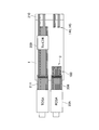
図1はネットワーク装置(不図示)に実装された本発明の第1の実施形態によるプリント回路基板を備える光送受信器の概略的断面斜視図を表している。図2は当該実施形態によるプリント回路基板の第一面を表している。図3は当該実施形態によるプリント回路基板の第二面を表している。なお図2,3中、本発明の要旨が曖昧になることを回避するため、受信側CDR IC(Rx-CDR IC)207と送信側CDR IC(Tx-CDR IC)209以外のICは省略されている。
[First Embodiment]
FIG. 1 shows a schematic cross-sectional perspective view of an optical transmitter / receiver including a printed circuit board according to a first embodiment of the present invention mounted on a network device (not shown). FIG. 2 shows the first surface of the printed circuit board according to the embodiment. FIG. 3 shows the second surface of the printed circuit board according to the embodiment. In FIGS. 2 and 3, ICs other than the receiving side CDR IC (Rx-CDR IC) 207 and the transmitting side CDR IC (Tx-CDR IC) 209 are omitted in order to avoid obscuring the gist of the present invention. ing.
光送受信器3はネットワーク装置のフロントパネル204に設けられた開口部に挿入される。光送受信器3はネットワーク装置のプリント回路基板203上に搭載されている。ネットワーク装置のプリント回路基板203上にはコネクタ208が設けられている。カードエッジ210はコネクタ208に係合される。カードエッジ210は上部ケース200と下部ケース201の後方のスロット開口部から外部に露出している。
The optical transmitter / receiver 3 is inserted into an opening provided in the
光送受信器3は、プリント回路基板(PCB:Printed Circuit Board)1、上部ケース200、下部ケース201、光受信サブアセンブリ(ROSA)205、光送信サブアセンブリ(TOSA:Transmitter Optical SubAssembly)(不図示)、ROSA側フレキシブルプリント基板(以下、FPC)206、TOSA側フレキシブル基板211、CDR IC207、及びカードエッジ210を有する。上部ケース200と下部ケース201は、カードエッジ210を通す部分の開口部以外の部分において隙間がないように密着することで光送受信器3のケースを構成する。光送受信器3のケースの内部には、ROSA205、TOSA、FPC(Flexible Printed Circuit)206,211、プリント回路基板1などが格納されている。ROSA205とTOSAはFPCを介してプリント回路基板1に接続されている。カードエッジ210はプリント回路基板1の一端側に設けられた配線パターンであり、カードエッジ210にはコネクタ208接続用の接点端子列が設けられている。FPC206上には4対の差動伝送線路が配置されている。プリント回路基板1上には複数のICが搭載されており、その一つに受信側のCDR IC207がある。
The optical transmitter / receiver 3 includes a printed circuit board (PCB) 1, an
光送受信器3のケースは、電子回路部品を搭載したプリント回路基板1を覆うことで電磁シールドとして機能する。上部ケース200及び下部ケース201の材料には亜鉛、アルミニウムなどの金属が用いられてよい。カードエッジ210は活線挿抜の機能を有する。コネクタ208はQSFP28 MSA規格に準拠している。ROSA205は4チャネルの光入力信号を電気信号に変換して増幅し、4チャネルの差動デジタル変調信号をビットレート25.78Gbit/sで外部端子に出力する。
The case of the optical transmitter / receiver 3 functions as an electromagnetic shield by covering the printed
当該実施形態におけるプリント回路基板1は、誘電体層の表面および内部に配線パターンが形成されたものと、複数の誘電体層の積層構造の両者を含む。本明細書では、誘電体の内部とは一つの誘電体の内部を示す場合と二つの誘電体層の間に挟まれた領域の両方を示すものとする。また誘電体と表記した場合は、単層の場合と複数層の場合の両者を含む。図2に図示されているように、プリント回路基板1の第一面にはFPC206,211、差動信号ビア列2、第一差動伝送線路100、差動信号ビア144,145、及びTx-CDR IC209が設けられている。また図3に図示されているように、プリント回路基板1の第二面には差動信号ビア列2、第二差動伝送線路110、差動信号ビア144,145、及びRx-CDR IC207が設けられている。第一面の第一差動伝送線路100と第二面の第二差動伝送線路110は、差動信号ビア列2を介して接続する。ここでは第一および第二差動伝送線路はそれぞれ4チャンネルを形成している。
The printed
ROSA205の外部端子は第三差動伝送線路が形成されたFPC206を介してプリント回路基板1の第一面上の第一差動伝送線路100に接続される。第一差動伝送線路100は差動信号ビア列2を介して第二面の第二差動伝送線路110と接続する。第二面の第二差動伝送線路110は第二面に配置されているRx−CDR IC207に接続される。図では4チャネル分の差動伝送線路が図示されているが4チャネル以外の複数のチャネル数であってもよい。
The external terminal of the
Rx-CDR IC207は4チャネル分の差動伝送線路と接続し、その内2チャネル分に相当する差動伝送線路が差動信号ビア144、145を介して表面である第一面の2チャネル分に相当する差動伝送線路を介してカードエッジ210に接続される。
The Rx-CDR IC207 is connected to 4 channels of differential transmission lines, of which 2 channels of differential transmission lines correspond to 2 channels on the front surface via differential signal vias 144 and 145. It is connected to the
TOSAもROSA同様にFPC211を介してプリント回路基板1の第一面に接続されている。TOSAは、プリント回路基板1においては第一面に設けられた差動伝送線路を介してTx−CDR209と接続されている。Tx−CDR209とカードエッジとは、第一面では2チャンネルを介して接続され、第二面では他の2チャンネルを介して接続されている。
Like ROSA, TOSA is also connected to the first surface of the printed
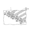
図4は当該実施形態によるプリント回路基板上に配置した4チャネルの差動信号ビア列2の斜視図を表している。図5は当該実施形態によるプリント回路基板上に配置した4チャネルの差動信号ビア列2の平面図を表している。図6は当該実施形態によるプリント回路基板のAA’線での概略的断面図を表している。図7は当該実施形態によるプリント回路基板のBB’線での概略的断面図を表している。
FIG. 4 shows a perspective view of a 4-channel differential signal via
図4に示されているように、差動信号ビア列2は4対の差動信号ビアと、10個の接地導体ビアと、接地導体ビアに接続した2つの接地導体層103,113と、接地導体層103,113に設けた開口120,121で構成される。4対の差動信号ビアは開口120,121内に設けられる。差動信号ビア列はプリント回路基板1の第一面上の4対の第一差動伝送線路100と第二面上の4対の第二差動伝送線路110とをそれぞれ接続する。ここでは4つのチャネルが構成される。例えば上記4つのチャネルは、ROSAから受信側CDR ICまでの間に配置され、4×25.78Gbit/sのシリアルデータを電気信号として伝達してよい。
As shown in FIG. 4, the differential signal via
ここでチャネル構造をよりよく理解するため、図示されている4つのチャネル(便宜上、左から第一乃至第四チャネルと指称する。)の内、差動信号ビア104,105で構成されるチャネル(第二チャネル)を例にとってチャネル構造を説明する。なお当該実施形態においては4つのチャネルの構成は、差動信号ビア付近においては寸法を含めて同一である。差動信号ビア104,105は一対の差動信号ビアを構成する。差動信号ビア104,105は、第一面の表面配線(第一ストリップ導体対)と第二面の表面配線(第二ストリップ導体対)とを接続する。D1は差動信号ビア104,105の中心間距離(差動信号ビアピッチ)を表す。当該実施形態においてD1は0.7mmだが他の値であってよい。当該実施形態において差動信号ビア104,105はドリル加工によるによるIVH(非貫通スルーホール)とレーザ加工によるLVH(レーザービアホール)との組合せで形成されてよいが、多層のプリント回路基板1の製造工程に応じて様々な方法で形成されてよい。当該実施形態においては、ビア(バイアホール)は、IVHでのドリル穴径を0.2mmとし、その穴の側面に銅メッキを施し、かつ、LVHでの穴径を0.1mmとし、その穴の側面に銅メッキを施すことで形成されてよい。
Here, in order to better understand the channel structure, of the four channels shown (referred to as the first to fourth channels from the left for convenience), the channel composed of the differential signal vias 104 and 105 (referred to as the first to fourth channels from the left) (for convenience). The channel structure will be described by taking the second channel) as an example. In the embodiment, the configurations of the four channels are the same in the vicinity of the differential signal via, including the dimensions. The
第一面の第一差動伝送線路100は、プリント回路基板1の表面に形成したストリップ導体101,102(第一ストリップ導体対)と、誘電体130の内部に形成された接地導体層103とで構成される。ストリップ導体101,102及び接地導体層103は銅箔をパターニングすることによって形成されてよい。第一差動伝送線路100はマイクロストリップライン型の伝送線路である。ストリップ導体101,102の導体幅及び導体間距離は、第一差動伝送線路100の差動特性インピーダンスが100Ωとなるように決定される。例えば誘電体の比誘電率が3.5、ストリップ導体101,102と接地導体層103との層間距離が0.166mmである場合、ストリップ導体101,102の導体幅及び導体間距離はそれぞれ0.19mm及び0.20mmとするのが好適である。ここでは4対の第一ストリップ導体対が配置されている(4チャンネルの第一差動伝送線路が形成されている)。
The first
プリント回路基板1の基材である誘電体130としては、ガラス布基材とエポキシ樹脂からなる材料(ガラスエポキシ樹脂)が用いられてよい。当該実施形態ではプリント回路基板1の厚さは1.0mmであるが、他の値であってもよい。
As the dielectric 130 which is the base material of the printed
プリント回路基板1の第一面とは反対の面である第二面の第二差動伝送線路110は第二面上に形成されたストリップ導体111,112(第二ストリップ導体対)と誘電体内部に形成した接地導体層113とで構成される。例えばストリップ導体111,112の寸法は、第一差動伝送線路100同様に、第二差動伝送線路110の差動特性インピーダンスが100Ωとなるように決定されてよい。
The second
4個の接地導体ビア106,107,108,109が、上方から見て長方形の頂点となるように配置され、差動信号ビア104,105からなる一対の差動信号ビアを取り囲む。接地導体ビア106,107の中心間距離D2は隣接するチャネル間の差動信号ビアの中心間距離(チャネルピッチ)Pと等しくてよい。当該実施形態ではD2は1.4mmである。当該実施形態では接地導体ビア107,108の中心間距離は1.4mmであるが、他の値であってもよい。
The four
接地導体層103,113内に設けられた開口(アンチパッド)120,121は、接地導体層103,113と差動信号ビアとを絶縁するために設けられる。隣接する第一乃至第四チャネルの全ての差動信号ビアは、開口120,121の各々を貫通するように配置される。第一乃至第四チャネルの差動信号ビアの対を構成する全ての差動信号ビアは、上方から見て一の方向に沿って配置される。好適には全ての差動信号ビアは一の直線上に配置される。
The openings (anti-pads) 120 and 121 provided in the ground conductor layers 103 and 113 are provided to insulate the ground conductor layers 103 and 113 from the differential signal via. All the differential signal vias of the adjacent first to fourth channels are arranged so as to penetrate each of the
第一乃至第四チャネルの差動信号ビアは、10個の接地導体ビアが4対の差動信号ビアを取り囲むように配置される。前記10個の接地導体ビアのうち2つの接地導体ビアは、隣接する差動信号ビア間で開口を挟んで対向するように配置される。つまり前記2つの接地導体ビアは前記隣接する差動信号ビアによって共有される。例えば第二チャネルの差動信号ビアと第三チャネルの差動信号ビアは、これらの間には接地導体ビア107,108が配置され、かつ、接地導体ビア107,108は第二チャネルの差動信号ビアと第三チャネルの差動信号ビアによって共有される。当該実施形態では、4対の差動信号ビアに対し10個の接地導体ビアが配置される。これら10個の接地導体ビアは開口120,121の外側において接地導体層103,113に接続される。接地導体ビアはそれぞれが取り囲む差動信号ビアの電磁界が広がらないようにする作用があり、接地導体ビアで取り囲むことで隣接するチャネル間のクロストークを減少させることができる。
The first to fourth channel differential signal vias are arranged such that ten ground conductor vias surround four pairs of differential signal vias. Two of the ten ground conductor vias are arranged so as to face each other with an opening between adjacent differential signal vias. That is, the two ground conductor vias are shared by the adjacent differential signal vias. For example, in the differential signal via of the second channel and the differential signal via of the third channel, the
当該実施形態の配置は、差動信号ビア列2の配置領域の面積を縮小することができる。当該実施形態では、第一乃至第四チャネルの差動信号ビアの各対内の差動信号ビアの中心間距離(差動信号ビアピッチ)D1は全て0.7mmである。また当該実施形態では、隣接するチャネル間の差動信号ビアの中心間距離(チャネルピッチ)Pは全て1.4mmである。また当該実施形態では、差動信号ビア列2の寸法はおよそ2.0mm×6.2mmである。
The arrangement of the embodiment can reduce the area of the arrangement area of the differential signal via
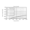
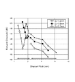
図8は、当該実施形態による差動信号ビア列における4チャネル間のフォワードクロストーク(Forward Crosstalk)特性のグラフを表している。当該実施形態による4チャネルの差動信号ビア列では、第一チャネルは差動ポート1と差動ポート2で構成され、第二チャネルは差動ポート3と差動ポート4で構成され、第三チャネルは差動ポート5と差動ポート6で構成され、かつ、第四チャネルは差動ポート7と差動ポート8で構成される。
FIG. 8 shows a graph of Forward Crosstalk characteristics between four channels in the differential signal via row according to the embodiment. In the 4-channel differential signal via row according to the embodiment, the first channel is composed of the
図中、St(Diff4,Diff1)は差動ポート1に入射して差動ポート4で検出されるフォワードクロストークを表し、St(Diff2,Diff3)は差動ポート3に入射して差動ポート2で検出されるフォワードクロストークを表し、St(Diff6,Diff1)は差動ポート1に入射して差動ポート6で検出されるフォワードクロストークを表し、St(Diff8,Diff1)は差動ポート1に入射して差動ポート8で検出されるフォワードクロストークを表し、St(Diff6,Diff3)は、差動ポート3に入射して差動ポート6で検出されるフォワードクロストークを表し、かつ、St(Diff8,Diff3)は差動ポート3に入射して差動ポート8で検出されるフォワードクロストークを表す。
In the figure, St (Diff4, Diff1) represents forward crosstalk incident on the
4チャネル(8ポート)の差動信号ビアの対称性を利用することで、6種類の組み合わせのみの検討で4チャネルの差動信号チャネル間のフォワードクロストーク特性を評価することができる。 By utilizing the symmetry of the 4-channel (8-port) differential signal via, it is possible to evaluate the forward crosstalk characteristics between the 4-channel differential signal channels by examining only 6 types of combinations.
図のフォワードクロストーク特性の周波数依存性は、三次元電磁界解析により求められた。その結果、フォワードクロストーク特性は、周波数範囲0〜25GHzという広い範囲において、最大でも−36dB以下の値に保たれており、極めて低いクロストーク量を持つ差動信号ビア列が実現されることが示された。 The frequency dependence of the forward crosstalk characteristics in the figure was obtained by three-dimensional electromagnetic field analysis. As a result, the forward crosstalk characteristic is maintained at a value of -36 dB or less at the maximum in a wide frequency range of 0 to 25 GHz, and a differential signal via train having an extremely low crosstalk amount can be realized. Shown.
[第二実施形態]
図9(a)は本発明の第2の実施形態によるプリント回路基板上に配置した2チャネルの差動信号ビア列の拡大平面図を表し、かつ、図9(b)は比較例1のプリント回路基板上に配置した2チャネルの差動信号ビア列の拡大平面図を表している。当該実施形態は、差動伝送線路のチャネル数が異なる点以外は、第1の実施形態と同じである。
[Second Embodiment]
FIG. 9A shows an enlarged plan view of a 2-channel differential signal via train arranged on the printed circuit board according to the second embodiment of the present invention, and FIG. 9B is a print of Comparative Example 1. It shows an enlarged plan view of a 2-channel differential signal via train arranged on a circuit board. The embodiment is the same as the first embodiment except that the number of channels of the differential transmission line is different.
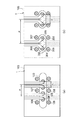
当該実施形態は図9(a)に示すように、差動信号ビア列は2対の差動信号ビアと、6個の接地導体ビアと、接地導体ビアに接続した2つの接地導体層と、接地導体層に設けたアンチパッドと呼ばれる開口120で構成される。隣接する第一及び第二のチャネルの全ての差動信号ビアは、一の開口120内で基板を貫通するように配置される。第一及び第二のチャネルの差動信号ビアの対を構成する全ての差動信号ビアは、上方から見て一の方向に沿って配置される。好適には全ての差動信号ビアは一の直線上に配置される。図9(a)では、6個の接地導体ビアが、第一及び第二のチャネルの差動信号ビアを取り囲むように配置される。前記6個の接地導体ビアのうち2個の接地導体ビアは、第一及び第二のチャネルの差動信号ビアの各対の間で開口120を挟んで対向するように配置される。具体的には、接地導体ビア107,108は、互いに隣接する第一チャネルの差動信号ビアと第二チャネルの差動信号ビアとの間で開口120を挟んで対向するように配置される。換言すれば、4個の接地導体ビアが差動信号ビアの各対を取り囲み、かつ、接地導体ビア107,108は、第一チャネルの差動信号ビアと第二チャネルの差動信号ビアによって共有される。これら6個の接地導体ビアは開口120の外側において接地導体層103に接続される。
In this embodiment, as shown in FIG. 9A, the differential signal via train consists of two pairs of differential signal vias, six ground conductor vias, and two ground conductor layers connected to the ground conductor vias. It is composed of an
2つのチャネルの内,図中の左側のチャネル(第一チャネル)を例にとってチャネル構造を説明する。4個の接地導体ビア106,107,108,109は、上方から見て長方形の頂点となるように配置されて差動信号ビア104,105からなる一対の差動信号ビアを取り囲む。接地導体ビア106,107の中心間距離は、隣接するチャネル間の差動信号ビアの中心間距離(チャネルピッチ)Pに等しくなるように設定される。当該実施形態では、接地導体ビア107,108の中心間距離は1.4mmに設定されるが他の値に設定されてもよい。なお第二チャネルの構成は、寸法を含めて第一チャネルと同一である。
Of the two channels, the channel structure will be described by taking the left channel (first channel) in the figure as an example. The four
第一及び第二のチャネルの差動信号ビアの各対内の差動信号ビアの中心間距離(差動信号ビアピッチ)D1は等しくなるように、後述の範囲の値から選ばれる。例えばD1は0.7mmが好適である。第一チャネルの差動信号ビアの中心位置と、第二チャネルの差動信号ビアの中心位置との間距離(チャネルピッチ)Pの値は後述の範囲から選ばれる。例えば好適にはPは1.4mmであるが他の値に設定されてもよい。これらの配置とすることにより、差動信号ビア列の配置領域の面積は非常に小さくなり得る。 The center-to-center distance (differential signal via pitch) D 1 of the differential signal vias in each pair of the differential signal vias of the first and second channels is selected from the values in the range described below so as to be equal. For example, D 1 is preferably 0.7 mm. The value of the distance (channel pitch) P between the center position of the differential signal via of the first channel and the center position of the differential signal via of the second channel is selected from the range described later. For example, P is preferably 1.4 mm, but may be set to another value. With these arrangements, the area of the arrangement area of the differential signal via train can be very small.
当該実施形態との比較のため、比較例1の構造が図9(b)に示されている。当該実施形態と比較例1との違いは2つある。第一の差異は、8個の接地導体ビアが2対の差動信号ビアを取り囲んでいる。つまり隣接する差動信号ビアの対の間に存在する接地導体ビアの個数は4個であり、8個の接地導体ビアのいずれも差動信号ビアの対によって共有されていないことである。図示されているように、差動信号ビアを取り囲む4個の接地導体ビア306,307,308,309は対をなす差動信号ビア304,305を取り囲むように配置されている。隣接する差動信号ビアの対と接地導体ビアも同様である。第二の差異は、差動信号ビアの各対がそれぞれ異なるアンチパッド(開口)を貫通するように配置されている点である。図示されているように、開口320を貫通するのは一つの差動伝送線路(一対のストリップ導体)とつながる差動信号ビアの対のみである。隣接する差動信号ビアの対と接地導体ビアも同様である。当該実施形態では、接地導体ビア306,307の中心間距離は1.4mmに設定され、接地導体ビア307,308の中心間距離は1.4mmに設定される。比較例1においては、例えば差動信号ビア304,305の中心間距離(差動信号ビアピッチ)D1は1.2mmに設定され、第一チャネルの差動信号ビアの中心位置と、第二チャネルの差動信号ビアの中心位置との間の距離(チャネルピッチ)Pは2.8mmに設定される。
The structure of Comparative Example 1 is shown in FIG. 9B for comparison with the embodiment. There are two differences between this embodiment and Comparative Example 1. The first difference is that eight ground conductor vias surround two pairs of differential signal vias. That is, the number of ground conductor vias existing between the pairs of adjacent differential signal vias is 4, and none of the eight ground conductor vias is shared by the pair of differential signal vias. As shown, the four
図10は、当該実施形態及び比較例1の差動信号ビア列におけるフォワードクロストーク量(最大値)のチャネルピッチ(P)依存性を比較したグラフを表している。縦軸は周波数範囲0〜25GHzにおけるフォワードクロストーク量の最大値であり、横軸はチャネルピッチPである。このグラフのフォワードクロストーク量の最大値とは、図5に示された差動信号ビア近傍でのフォワードクロストークの最大値である。具体的には、この最大値は、差動信号線と差動信号ビア全体のSパラメータ行列から、マイクロストリップラインの寄与を取り除いたSパラメータを行列演算により算出して求めたフォワードクロストーク量の最大値である。 FIG. 10 shows a graph comparing the channel pitch (P) dependence of the forward crosstalk amount (maximum value) in the differential signal via sequence of the embodiment and Comparative Example 1. The vertical axis is the maximum value of the forward crosstalk amount in the frequency range of 0 to 25 GHz, and the horizontal axis is the channel pitch P. The maximum value of the forward crosstalk amount in this graph is the maximum value of the forward crosstalk in the vicinity of the differential signal via shown in FIG. Specifically, this maximum value is the amount of forward crosstalk obtained by calculating the S-parameters of the entire differential signal line and differential signal via by removing the contribution of the microstrip line by matrix calculation. The maximum value.
図10は、差動信号ビアピッチD1が1.2mm、1.0mm、0.7mmに設定された場合において、チャネルピッチPの変化に対するフォワードクロストーク量の変化を表す6本の曲線を示している。Pが2.3mm以上の配置は比較例1に相当し、Pが2.1mm以下の配置は当該実施形態に相当する。 FIG. 10 shows six curves showing the change in the amount of forward crosstalk with respect to the change in the channel pitch P when the differential signal via pitch D 1 is set to 1.2 mm, 1.0 mm, and 0.7 mm. There is. An arrangement in which P is 2.3 mm or more corresponds to Comparative Example 1, and an arrangement in which P is 2.1 mm or less corresponds to the embodiment.
本願発明者の検討によれば、比較例1の構造ではチャネルピッチPを小さくするに従って、フォワードクロストーク量は単調に増大し、比較例1の構造で実際に実現可能なチャネルピッチPの最小寸法である2.3mmにおいて最も大きな値を示した。またこれらの差動信号ビア間のフォワードクロストークは、位相の変化の振る舞いより、容量性結合が支配的要因であることがわかっている。 According to the study of the inventor of the present application, in the structure of Comparative Example 1, as the channel pitch P is decreased, the amount of forward crosstalk increases monotonically, and the minimum dimension of the channel pitch P that can be actually realized in the structure of Comparative Example 1 The largest value was shown at 2.3 mm. It is also known that the forward crosstalk between these differential signal vias is dominated by the capacitive coupling rather than the behavior of the phase change.
差動信号ビアピッチD1については1.2mmとすることにより、差動信号ビア部での特性インピーダンスを100Ωに一致させることが容易にでき、伝達特性を良好に保つ上では理想的であった。比較例1では上記のように、差動信号ビアピッチD1を1.2mm、チャネルピッチPを2.8mmとすることで、フォワードクロストーク量の最大値を−38dBと良好にし、かつ伝達特性を良好に保つことができる。しかしチャネルピッチPを大幅に縮小することは困難であり、これ以上の高密度実装は困難であることがわかった。 By setting the differential signal via pitch D 1 to 1.2 mm, the characteristic impedance at the differential signal via portion can be easily matched to 100Ω, which is ideal for maintaining good transmission characteristics. In Comparative Example 1, as described above, by setting the differential signal via pitch D 1 to 1.2 mm and the channel pitch P to 2.8 mm, the maximum value of the forward crosstalk amount is set to -38 dB, and the transmission characteristics are improved. Can be kept good. However, it has been found that it is difficult to significantly reduce the channel pitch P, and it is difficult to mount at a higher density.
当該実施形態の構造では実際に製造できるチャネルピッチPの最小寸法は、差動信号ビアピッチD1にも依存するが、2.1mmよりさらに小さくすることができる。また差動信号ビアピッチD1が1.2mmの場合には、チャネルピッチPが小さくなるに従って、フォワードクロストーク量が急激に増大した。一方本願発明者は検討の結果、差動信号ビアピッチD1が0.7mmの場合には、チャネルピッチPを2.1mmから小さくしてゆくと、フォワードクロストーク量が一度極小値を示した後、増大することを見出した。この急増を示す領域−例えばチャネルピッチPが1.2mmの場合−では、差動信号ビア間の結合は誘導性を示した。極小値をとるチャネルピッチP(1.5mm)の前後の領域では、差動信号ビア間の結合は容量性から誘導性への変化の途中の特性を示している。つまりPが1.5mm前後の領域では、差動信号ビア間の結合が容量性から誘導性へ遷移している。よって、この遷移領域において容量性結合と誘導性結合の相殺効果が生じているものと考えられる。差動信号ビアピッチD1については0.7mmの場合でも、差動信号ビアでの寄生容量を低減することにより、差動反射特性を−20dB程度に低減し、かつ、伝達特性を良好にすることが可能であった。当該実施形態は、上記のように、差動信号ビアピッチD1を0.7mm、チャネルピッチPを1.4mmと大幅に縮小しても、フォワードクロストーク量の最大値を−39dBと良好にし、かつ伝達特性を良好に保つことを可能にする。 In the structure of the embodiment, the minimum dimension of the channel pitch P that can be actually manufactured depends on the differential signal via pitch D 1 , but can be made smaller than 2.1 mm. When the differential signal via pitch D 1 was 1.2 mm, the amount of forward crosstalk increased sharply as the channel pitch P decreased. On the other hand, as a result of the examination, the inventor of the present application shows that when the differential signal via pitch D 1 is 0.7 mm, the forward crosstalk amount once shows a minimum value when the channel pitch P is reduced from 2.1 mm. , Found to increase. In the region showing this rapid increase-for example, when the channel pitch P is 1.2 mm-the coupling between the differential signal vias was inductive. In the region before and after the channel pitch P (1.5 mm), which takes a minimum value, the coupling between the differential signal vias shows a characteristic in the middle of the change from capacitive to inductive. That is, in the region where P is around 1.5 mm, the coupling between the differential signal vias transitions from capacitive to inductive. Therefore, it is considered that the canceling effect of the capacitive coupling and the inducible coupling occurs in this transition region. Even when the differential signal via pitch D 1 is 0.7 mm, the differential reflection characteristic is reduced to about -20 dB and the transmission characteristic is improved by reducing the parasitic capacitance in the differential signal via. Was possible. In the embodiment, as described above, even if the differential signal via pitch D 1 is significantly reduced to 0.7 mm and the channel pitch P is significantly reduced to 1.4 mm, the maximum value of the forward crosstalk amount is as good as −39 dB. And it makes it possible to maintain good transmission characteristics.
次に当該実施形態において、上記のメカニズムに基づく相殺効果が得られ、フォワードクロストークを充分に抑圧できるための差動信号ビアピッチD1とチャネルピッチPの範囲について説明する。図11は当該実施形態の差動信号ビア列における2チャネル間のフォワードクロストーク量(最大値)の差動信号ビアピッチ(D1)とチャネルピッチ(P)に対する等値線を示すグラフを表している。図11において、差動信号ビアピッチD1を0.6mmから1.2mmの範囲で変化させ、かつ、チャネルピッチPを1.0mmから2.2mmの範囲で変化させたときのフォワードクロストーク量(最大値)を三次元電磁解析により求め、差動信号ビアピッチD1をx座標、チャネルピッチPをy座標として、その結果を等値線図にしたものである。 Next, in the embodiment, the ranges of the differential signal via pitch D 1 and the channel pitch P for obtaining the canceling effect based on the above mechanism and sufficiently suppressing the forward crosstalk will be described. FIG. 11 shows a graph showing contour lines for the differential signal via pitch (D 1 ) and the channel pitch (P) of the forward crosstalk amount (maximum value) between two channels in the differential signal via sequence of the embodiment. There is. In FIG. 11, the amount of forward crosstalk (when the differential signal via pitch D 1 is changed in the range of 0.6 mm to 1.2 mm and the channel pitch P is changed in the range of 1.0 mm to 2.2 mm). The maximum value) was obtained by three-dimensional electromagnetic analysis, the differential signal via pitch D 1 was set to the x coordinate, and the channel pitch P was set to the y coordinate, and the results were plotted in a contour diagram.
図11より、座標(0.7mm,1.5mm)を中心とした比較的小さな領域で最も大きな効果が得られ、この領域ではフォワードクロストーク量の最大値を−45dB以下に抑圧できることがわかる。またフォワードクロストーク量の最大値は、光送受信器を搭載するネットワーク装置やシステムの仕様にも依るが、例えば−35dB以下であれば充分良好な特性である。当該実施形態においては、各対を構成する2つの前記差動信号ビアの中心間距離D1、前記隣接する2つの対の中心間距離Pとする場合、(D1,P)が、(0.6mm,1.2mm)、(0.9mm,1.6mm)、(1.2mm,2.2mm)、(0.6mm,2.2mm)を頂点とする四角形の辺上又は該四角形の範囲の側に位置することにより、所望の特性が実現できることがわかる。なお、本特性はチャネル数によらず同様の効果を得ることができる。つまり第1の実施形態で示したように4チャンネルの差動信号ビアの対が配置されるものであっても、図11の関係であり、所望する特性に応じてチャネルピッチP、差動信号ビアピッチD1を選択すればよい。 From FIG. 11, it can be seen that the greatest effect is obtained in a relatively small region centered on the coordinates (0.7 mm, 1.5 mm), and the maximum value of the forward crosstalk amount can be suppressed to −45 dB or less in this region. The maximum value of the forward crosstalk amount depends on the specifications of the network device and system equipped with the optical transmitter / receiver, but for example, if it is −35 dB or less, it is a sufficiently good characteristic. In the embodiment, when the center-to-center distance D 1 of the two differential signal vias constituting each pair and the center-to-center distance P of the two adjacent pairs are set, (D 1 , P) is (0). .6mm, 1.2mm), (0.9mm, 1.6mm), (1.2mm, 2.2mm), (0.6mm, 2.2mm) on the side of the quadrangle or the range of the quadrangle It can be seen that the desired characteristics can be realized by being located on the side of. This characteristic can obtain the same effect regardless of the number of channels. That is, even if a pair of 4-channel differential signal vias is arranged as shown in the first embodiment, the relationship is shown in FIG. 11, and the channel pitch P and the differential signal are set according to the desired characteristics. The via pitch D 1 may be selected.
以上のように当該実施形態によれば、プリント回路基板上の第一面に接続したFPCと第二面に搭載したCDR ICとを備える光送受信器は、ROSAから受信側CDR ICに至る2チャネルの差動信号のクロストーク量を低減し、かつ配置領域の面積を縮小し、高速化と高密度実装が可能なプリント回路基板構造を実現する。つまり比較例1で示したように隣接する差動伝送線路においては、接地導体層に設けられた開口は一つの差動信号ビアごとに設ける程度の距離を離さないと十分なクロストーク特性を得ることができなかった。しかし本発明者は鋭意検討することで、チャネルピッチPを近づけても十分なクロストーク特性を得られることを見出した。その結果、隣接する差動信号ビアの対を二つとも接地導体層に設けられた単一の開口に入るように配置することが可能となり、差動信号ビア列の面積を非常に縮小させることができた。さらに、各差動信号ビアを取り囲む接地導体ビアのうち、隣接チャネルの間にある二つ接地導体ビアを共用しても優れた特性を得ることができ、小型化を実現できる。その結果当該実施形態は、受信波形品位の確保と小型化を両立したプリント回路基板およびそのプリント回路基板を備える光送受信器を提供することができる。 As described above, according to the embodiment, the optical transmitter / receiver including the FPC connected to the first surface on the printed circuit board and the CDR IC mounted on the second surface has two channels from ROSA to the receiving side CDR IC. The amount of crosstalk of the differential signal is reduced, the area of the arrangement area is reduced, and a printed circuit board structure capable of high speed and high density mounting is realized. That is, as shown in Comparative Example 1, in the adjacent differential transmission lines, sufficient crosstalk characteristics can be obtained unless the openings provided in the ground conductor layer are separated by a distance provided for each differential signal via. I couldn't. However, the present inventor has found that sufficient crosstalk characteristics can be obtained even when the channel pitch P is brought close to each other through diligent studies. As a result, both pairs of adjacent differential signal vias can be arranged so as to fit into a single opening provided in the ground conductor layer, greatly reducing the area of the differential signal via train. Was done. Further, among the ground conductor vias surrounding each differential signal via, excellent characteristics can be obtained even if two ground conductor vias between adjacent channels are shared, and miniaturization can be realized. As a result, the embodiment can provide a printed circuit board having both ensured reception waveform quality and miniaturization, and an optical transmitter / receiver including the printed circuit board.
第2の実施形態においてはプリント回路基板に配置した差動伝送線路と差動信号ビアを2チャネルとし、また第1の実施形態ではプリント回路基板上に配置した差動伝送線路と差動信号ビアを4チャネルとしたが、隣接する複数のチャネルの数は2,4以外であっても良い。隣接する複数のチャネルの数をN(Nは2以上の整数)とした場合には、N対の差動信号ビアに対しその周囲に合計(2N+2)個の接地導体ビアが配置され、2つの接地導体ビアは隣接する2つのチャネルの間で開口を挟んで対向するように配置され、前記2つの接地導体ビアは前記隣接する2つのチャネルによって共有され、前記2つの接地導体ビアは前記開口の外側において前記接地導体層に接続される。 In the second embodiment, the differential transmission line and the differential signal via arranged on the printed circuit board have two channels, and in the first embodiment, the differential transmission line and the differential signal via arranged on the printed circuit board have two channels. Is set to 4 channels, but the number of adjacent plurality of channels may be other than 2 and 4. When the number of adjacent multiple channels is N (N is an integer of 2 or more), a total of (2N + 2) ground conductor vias are arranged around the N pairs of differential signal vias. The two ground conductor vias are arranged so as to face each other with an opening between two adjacent channels, the two ground conductor vias are shared by the two adjacent channels, and the two ground conductor vias are said. It is connected to the ground conductor layer outside the opening.
次に本発明の効果を述べるため、図12,13を参照しながら比較例2を説明する。図12は比較例2のプリント回路基板上に配置した4チャネルの差動伝送線路と差動信号ビアの斜視図を表し、図13は比較例2のプリント回路基板上に配置した4チャネルの差動信号ビア列の平面図を表す。 Next, in order to describe the effect of the present invention, Comparative Example 2 will be described with reference to FIGS. 12 and 13. FIG. 12 shows a perspective view of a 4-channel differential transmission line and a differential signal via arranged on the printed circuit board of Comparative Example 2, and FIG. 13 shows a difference of 4 channels arranged on the printed circuit board of Comparative Example 2. Represents a plan view of a row of dynamic signal vias.
比較例2は、2組の比較例1の配置の高密度化を図った4チャネルの差動信号ビア列である。比較例2では、隣接する2チャネルの差動信号ビア列2組は互い違いになるように前後に配置され、隣接するチャネルの間に位置する導体接地ビア3個は共有される。この構造にすることにより、差動伝送線路100の延伸方向に対し垂直な方向でのチャネルピッチPを1.4mmとすることができる。この値は上記第1の実施形態と等しい値である。我々の検討によれば、比較例2における4チャネル間の差動モードのフォワードクロストーク特性は、6通りの組合せのうち、第二チャネルと第三チャネル間、第一チャネルと第四チャネル間のクロストーク特性が最大値を示した。その値は上記比較例1の場合と等しいものであり、良好な特性が得られた。しかし差動信号ビア列302のサイズはおよそ3.4mm×6.2mmであり、上記比較例2での差動信号ビア列2のサイズはおよそ2.0mm×6.2mmには面積縮小の点で及ばなかった。
Comparative Example 2 is a 4-channel differential signal via sequence in which the arrangement of the two sets of Comparative Example 1 is densified. In Comparative Example 2, two sets of differential signal vias of two adjacent channels are arranged in the front and rear so as to be staggered, and three conductor grounding vias located between the adjacent channels are shared. With this structure, the channel pitch P in the direction perpendicular to the extending direction of the
以上のように、第1の実施形態は、高密度化を図った比較例2に比べても、配置領域の面積を縮小することができ、差動信号のクロストーク量の低減と、高速化と高密度実装が可能なプリント回路基板構造を実現する。その結果第1の実施形態は、受信波形品位の確保と小型化を両立したプリント回路基板およびそのプリント回路基板を備える光送受信器を提供することができる。 As described above, in the first embodiment, the area of the arrangement region can be reduced as compared with Comparative Example 2 in which the density is increased, the crosstalk amount of the differential signal is reduced, and the speed is increased. Achieves a printed circuit board structure that enables high-density mounting. As a result, the first embodiment can provide a printed circuit board having both a ensured reception waveform quality and miniaturization, and an optical transmitter / receiver including the printed circuit board.
第1、第2の実施形態では、ROSAと接続される差動伝送線路に関して説明したがこれに限られず、プリント回路基板の第一面から第二面へと繋がる差動信号ビア列について広く適用することができる。また第二面の差動伝送線路はCDR ICと接続されていたが、これに限られず他のIC、例えばDSP(Digital Signal Processor)などであっても本発明の効果は得られる。 In the first and second embodiments, the differential transmission line connected to the ROSA has been described, but the present invention is not limited to this, and the differential signal via train connected from the first surface to the second surface of the printed circuit board is widely applied. can do. Further, the differential transmission line on the second surface is connected to the CDR IC, but the effect of the present invention can be obtained not only by this but also by other ICs such as DSP (Digital Signal Processor).
1 プリント回路基板、2 差動信号ビア列、3 光送受信器、100 第一差動伝送線路、101,102 ストリップ導体、103 接地導体層、104,105、144、145 差動信号ビア、106,107,108,109 接地導体ビア、110 第二差動伝送線路、111,112 ストリップ導体、113 接地導体層、120,121 開口(アンチパッド)、130 誘電体、200 上部ケース、201 下部ケース、203 (ネットワーク装置の)プリント回路基板(PCB)、204 (ネットワーク装置の)フロントパネル、205 光受信サブアセンブリ(ROSA)、206 ROSA側フレキシブルプリント基板(FPC)、207,209 IC、208 コネクタ、210 カードエッジ、211 TOSA側フレキシブル基板、302 差動信号ビア列、304,305 差動信号ビア、306,307,308,309 接地導体ビア、320 開口。 1 printed circuit board, 2 differential signal via train, 3 optical transmitter / receiver, 100 first differential transmission line, 101, 102 strip conductor, 103 ground conductor layer, 104, 105, 144, 145 differential signal via, 106, 107, 108, 109 Ground conductor via, 110 Second differential transmission line, 111, 112 Strip conductor, 113 Ground conductor layer, 120, 121 openings (anti-pad), 130 dielectric, 200 upper case, 201 lower case, 203 Printed Circuit Board (PCB), 204 Front Panel (of Network Equipment), 205 Optical Reception Subassembly (ROSA), 206 ROSA Side Flexible Printed Circuit Board (FPC), 207,209 IC, 208 Connector, 210 Cards Edge, 211 TOSA side flexible board, 302 differential signal via row, 304,305 differential signal via, 306,307,308,309 ground conductor via, 320 openings.
Claims (8)
前記誘電体を貫通するように設けられるN個(Nは2以上の整数)の差動信号ビアの対と、
前記誘電体の第一面上に設けられるN個の第一ストリップ導体対と、
前記誘電体の内部に設けられて前記N個の第一ストリップ導体対および前記誘電体とそれぞれN個の第一差動伝送線路を構成する第一接地導体層と、
前記誘電体の第二面上に設けられるN個の第二ストリップ導体対と、
前記誘電体の内部に設けられて前記N個の第二ストリップ導体対および前記誘電体とそれぞれN個の第二差動伝送線路を構成する第二接地導体層と、
前記第一及び第二接地導体層にそれぞれ接続する複数の接地導体ビアと、
を有し、
前記N個の第一ストリップ導体対と第二ストリップ導体対は前記N個の差動信号ビアの対を介して各々が接続され、
前記第一接地導体層は、前記N個の差動信号ビアの対と絶縁するための単一の第一開口を備え、前記第二接地導体層は、前記N個の差動信号ビアの対と絶縁するための単一の第二開口を備え、
前記N個の差動信号ビアの対は、前記単一の第一及び第二開口を貫通するとともに、前記第一及び第二開口内で一の方向に沿って配置され、
前記複数の接地導体ビアは、前記N個の差動信号ビアの対を取り囲むように、かつ、前記第一及び第二開口の外側に配置される、
プリント回路基板。 Dielectric and
A pair of N differential signal vias (N is an integer of 2 or more) provided so as to penetrate the dielectric, and
N first strip conductor pairs provided on the first surface of the dielectric and
The N first strip conductor pairs provided inside the dielectric and the first ground conductor layer constituting the dielectric and N first differential transmission lines, respectively.
N second strip conductor pairs provided on the second surface of the dielectric and
The N second strip conductor pair provided inside the dielectric and the second ground conductor layer constituting the dielectric and N second differential transmission lines, respectively.
A plurality of ground conductor vias connected to the first and second ground conductor layers, respectively,
Have,
The N first strip conductor pair and the second strip conductor pair are connected to each other via the pair of the N differential signal vias.
Said first ground conductor layer is provided with a single first opening for insulating the pair of the N differential signal vias, the second grounding conductor layer, said pair of N differential signal vias With a single second opening for insulation with
The pair of N differential signal vias penetrates the single first and second openings and is arranged along one direction within the first and second openings .
The plurality of ground conductor vias are arranged so as to surround the pair of the N differential signal vias and outside the first and second openings.
Printed circuit board.
前記複数の接地導体ビアは、前記N個の差動信号ビアの対のそれぞれを取り囲むように配置される(2N+2)個の接地導体ビアを含み、
前記(2N+2)個の接地導体ビアのうちの2個の接地導体ビアは、前記N個の差動信号ビアの対のうちの隣接する2つの差動信号ビアの対との間に、前記第一及び第二開口を挟んで対向するよう配置され、
前記(2N+2)個の接地導体ビアは前記第一及び第二開口の外側において前記第一及び第二接地導体層に接続する、
ことを特徴とするプリント回路基板。 The printed circuit board according to claim 1.
It said plurality of grounding conductor vias includes the N is disposed so as to surround the respective pair of differential signal vias (2N + 2) pieces of the ground conductor vias,
Two ground conductor vias of the (2N + 2) ground conductor vias are placed between two adjacent differential signal via pairs of the N differential signal vias. Arranged so as to face each other across the first and second openings.
The (2N + 2) ground conductor vias connect to the first and second ground conductor layers outside the first and second openings.
A printed circuit board characterized by that.
前記N個の差動信号ビアの対のうち、隣接する二つの差動信号ビアの対の中心間距離D1、前記隣接する二つの差動信号ビアの対に接続される隣接する二つの第一差動伝送線路の中心間距離Pとする場合、(D1,P)は、(0.6mm,1.2mm)、(0.9mm,1.6mm)、(1.2mm,2.2mm)、(0.6mm,2.2mm)を頂点とする四角形の辺上又は該四角形の範囲の内側に位置する、
ことを特徴とするプリント回路基板。 The printed circuit board according to claim 1.
Of the N pairs of differential signal vias, the center-to-center distance D1 of the pair of two adjacent differential signal vias, and the two adjacent first pairs connected to the pair of the two adjacent differential signal vias. When the distance between the centers of the differential transmission line is P, (D1, P) are (0.6 mm, 1.2 mm), (0.9 mm, 1.6 mm), (1.2 mm, 2.2 mm), (0.6 mm, 2.2 mm) positioned on the inner side of the edge or on the scope of the rectangular quadrangle whose vertices,
A printed circuit board characterized by that.
前記誘電体を貫通するように設けられるN個(Nは2以上の整数)の差動信号ビアの対と、
前記誘電体の第一面上に設けられるN個の第一ストリップ導体対と、
前記誘電体の内部に設けられて前記N個の第一ストリップ導体対および前記誘電体とそれぞれN個の第一差動伝送線路を構成する第一接地導体層と、
前記誘電体の第二面上に設けられるN個の第二ストリップ導体対と、
前記誘電体の内部に設けられて前記N個の第二ストリップ導体対および前記誘電体とそれぞれN個の第二差動伝送線路を構成する第二接地導体層と、
を有し、
前記N個の第一ストリップ導体対と第二ストリップ導体対は前記N個の差動信号ビアの対を介して各々が接続され、
前記N個の差動信号ビアの対のうち、隣接する二つの差動信号ビアの対の中心間距離D1、前記隣接する二つの差動信号ビアの対に接続される隣接する二つの第一差動伝送線路の中心間距離Pとする場合、(D1,P)は、(0.6mm,1.2mm)、(0.9mm,1.6mm)、(1.2mm,2.2mm)、(0.6mm,2.2mm)を頂点とする四角形の辺上又は該四角形の範囲の内側に位置する、
ことを特徴とするプリント回路基板。 Dielectric and
A pair of N differential signal vias (N is an integer of 2 or more) provided so as to penetrate the dielectric, and
N first strip conductor pairs provided on the first surface of the dielectric and
The N first strip conductor pairs provided inside the dielectric and the first ground conductor layer constituting the dielectric and N first differential transmission lines, respectively.
N second strip conductor pairs provided on the second surface of the dielectric and
The N second strip conductor pair provided inside the dielectric and the second ground conductor layer constituting the dielectric and N second differential transmission lines, respectively.
Have,
The N first strip conductor pair and the second strip conductor pair are connected to each other via the pair of the N differential signal vias.
Of the N pairs of differential signal vias, the center-to-center distance D1 of the pair of two adjacent differential signal vias, and the two adjacent first pairs connected to the pair of the two adjacent differential signal vias. When the distance between the centers of the differential transmission line is P, (D1, P) are (0.6 mm, 1.2 mm), (0.9 mm, 1.6 mm), (1.2 mm, 2.2 mm), (0.6 mm, 2.2 mm) positioned on the inner side of the edge or on the scope of the rectangular quadrangle whose vertices,
A printed circuit board characterized by that.
前記第一接地導体層は、前記N個の差動信号ビアの対と絶縁するための単一の第一開口を備え、前記第二接地導体層は、前記N個の差動信号ビアの対と絶縁するための単一の第二開口を備え、
前記N個の差動信号ビアの対は、前記単一の第一及び第二開口を貫通するとともに、前記第一及び第二開口内で一の方向に沿って配置される、
ことを特徴とするプリント回路基板。 The printed circuit board according to claim 4.
Said first ground conductor layer is provided with a single first opening for insulating the pair of the N differential signal vias, the second grounding conductor layer, said pair of N differential signal vias With a single second opening for insulation with
The pair of N differential signal vias penetrates the single first and second openings and is arranged along one direction within the first and second openings.
A printed circuit board characterized by that.
前記N個の差動信号ビアの対のそれぞれを取り囲むように配置される(2N+2)個の接地導体ビアをさらに有し、
前記(2N+2)個の接地導体ビアのうちの2個の接地導体ビアは、前記N個の差動信号ビアの対のうちの隣接する2つの差動信号ビアの対との間に、前記第一及び第二開口を挟んで対向するよう配置され、
前記(2N+2)個の接地導体ビアは前記第一及び第二開口の外側において前記第一及び第二接地導体層に接続する、
ことを特徴とするプリント回路基板。 The printed circuit board according to claim 5.
It further has (2N + 2) ground conductor vias arranged to surround each of the pairs of N differential signal vias.
Two ground conductor vias of the (2N + 2) ground conductor vias are placed between two adjacent differential signal via pairs of the N differential signal vias. Arranged so as to face each other across the first and second openings.
The (2N + 2) ground conductor vias connect to the first and second ground conductor layers outside the first and second openings.
A printed circuit board characterized by that.
光信号を出力する光送信サブアセンブリと、
入力される光信号を電気信号に変換する光受信サブアセンブリと、
N個の第三差動伝送線路が形成されたフレキシブル基板と、
ICと、
前記プリント回路基板、前記光受信サブアセンブリ、前記フレキシブル基板、そして前記ICを格納するケースと、をさらに備え、
前記電気信号は、前記フレキシブル基板の前記第三差動伝送線路を介して前記プリント回路基板の前記第一差動伝送線路に接続される、
ことを特徴とする光送受信器。 The optical transmitter / receiver according to claim 7.
An optical transmission subassembly that outputs an optical signal,
An optical receiving subassembly that converts an input optical signal into an electrical signal,
A flexible board on which N third differential transmission lines are formed,
IC and
The printed circuit board, the optical receiving subassembly, the flexible board, and a case for storing the IC are further provided.
The electric signal is connected to the first differential transmission line of the printed circuit board via the third differential transmission line of the flexible board.
An optical transmitter / receiver characterized by that.
Priority Applications (3)
| Application Number | Priority Date | Filing Date | Title |
|---|---|---|---|
| JP2017223643A JP6894352B2 (en) | 2017-11-21 | 2017-11-21 | A printed circuit board and an optical transmitter / receiver provided with the printed circuit board. |
| US16/185,036 US10470293B2 (en) | 2017-11-21 | 2018-11-09 | Printed circuit board and optical transceiver with the printed circuit board |
| US16/673,239 US11057986B2 (en) | 2017-11-21 | 2019-11-04 | Printed circuit board and optical transceiver with the printed circuit board |
Applications Claiming Priority (1)
| Application Number | Priority Date | Filing Date | Title |
|---|---|---|---|
| JP2017223643A JP6894352B2 (en) | 2017-11-21 | 2017-11-21 | A printed circuit board and an optical transmitter / receiver provided with the printed circuit board. |
Publications (3)
| Publication Number | Publication Date |
|---|---|
| JP2019096691A JP2019096691A (en) | 2019-06-20 |
| JP2019096691A5 JP2019096691A5 (en) | 2021-01-07 |
| JP6894352B2 true JP6894352B2 (en) | 2021-06-30 |
Family
ID=66534686
Family Applications (1)
| Application Number | Title | Priority Date | Filing Date |
|---|---|---|---|
| JP2017223643A Active JP6894352B2 (en) | 2017-11-21 | 2017-11-21 | A printed circuit board and an optical transmitter / receiver provided with the printed circuit board. |
Country Status (2)
| Country | Link |
|---|---|
| US (2) | US10470293B2 (en) |
| JP (1) | JP6894352B2 (en) |
Families Citing this family (4)
| Publication number | Priority date | Publication date | Assignee | Title |
|---|---|---|---|---|
| JP6894352B2 (en) | 2017-11-21 | 2021-06-30 | 日本ルメンタム株式会社 | A printed circuit board and an optical transmitter / receiver provided with the printed circuit board. |
| JP7151567B2 (en) * | 2019-03-14 | 2022-10-12 | 株式会社オートネットワーク技術研究所 | Connection structure between circuit device and electronic control unit and circuit device |
| CN113133186A (en) * | 2021-04-15 | 2021-07-16 | 山东英信计算机技术有限公司 | High-density connector PCB structure based on PCIe 5.0 protocol |
| US11924964B2 (en) * | 2022-04-07 | 2024-03-05 | Western Digital Technologies, Inc. | Printed circuit board for galvanic effect reduction |
Family Cites Families (13)
| Publication number | Priority date | Publication date | Assignee | Title |
|---|---|---|---|---|
| JP4354489B2 (en) * | 2004-02-13 | 2009-10-28 | モレックス インコーポレイテド | Circuit board and high-speed via system |
| JP2005243864A (en) * | 2004-02-26 | 2005-09-08 | Kyocera Corp | Wiring board |
| JP4852979B2 (en) * | 2005-10-31 | 2012-01-11 | ソニー株式会社 | Flex-rigid board, optical transceiver module and optical transceiver |
| JP4930590B2 (en) * | 2006-10-13 | 2012-05-16 | 日本電気株式会社 | Multilayer board |
| US7999192B2 (en) * | 2007-03-14 | 2011-08-16 | Amphenol Corporation | Adjacent plated through holes with staggered couplings for crosstalk reduction in high speed printed circuit boards |
| JP4625822B2 (en) * | 2007-03-16 | 2011-02-02 | 株式会社東芝 | Semiconductor memory device and manufacturing method thereof |
| WO2008133010A1 (en) * | 2007-04-12 | 2008-11-06 | Nec Corporation | Filter circuit element and electronic circuit device |
| JP4892514B2 (en) * | 2008-04-22 | 2012-03-07 | 日本オプネクスト株式会社 | Optical communication module and flexible printed circuit board |
| JP5216147B2 (en) * | 2011-03-08 | 2013-06-19 | 日本オクラロ株式会社 | Differential transmission circuit, optical transceiver module, and information processing apparatus |
| JP2014138015A (en) | 2013-01-15 | 2014-07-28 | Fujitsu Ltd | Printed board and method for manufacturing printed board |
| CN104937767B (en) * | 2013-01-24 | 2018-01-19 | 日本电气株式会社 | Printed substrate, electronic device and line connecting method |
| US9554455B2 (en) | 2014-06-09 | 2017-01-24 | Hirose Electric Co., Ltd. | Method and apparatus for reducing far-end crosstalk in electrical connectors |
| JP6894352B2 (en) | 2017-11-21 | 2021-06-30 | 日本ルメンタム株式会社 | A printed circuit board and an optical transmitter / receiver provided with the printed circuit board. |
-
2017
- 2017-11-21 JP JP2017223643A patent/JP6894352B2/en active Active
-
2018
- 2018-11-09 US US16/185,036 patent/US10470293B2/en active Active
-
2019
- 2019-11-04 US US16/673,239 patent/US11057986B2/en active Active
Also Published As
| Publication number | Publication date |
|---|---|
| US10470293B2 (en) | 2019-11-05 |
| US20200068703A1 (en) | 2020-02-27 |
| JP2019096691A (en) | 2019-06-20 |
| US20190159334A1 (en) | 2019-05-23 |
| US11057986B2 (en) | 2021-07-06 |
Similar Documents
| Publication | Publication Date | Title |
|---|---|---|
| JP6894352B2 (en) | A printed circuit board and an optical transmitter / receiver provided with the printed circuit board. | |
| US7999192B2 (en) | Adjacent plated through holes with staggered couplings for crosstalk reduction in high speed printed circuit boards | |
| US7448880B2 (en) | Multilayer printed circuit board for high-speed differential signal, communication apparatus, and data storage apparatus | |
| US9781824B2 (en) | Differential transmission circuit, optical module and manufacturing method of differential transmission circuit | |
| US20100259338A1 (en) | High frequency and wide band impedance matching via | |
| JP6388667B2 (en) | Apparatus and method for transmitting differential data signals | |
| JP5983780B2 (en) | Printed wiring board, electronic device and wiring connection method | |
| US10904997B2 (en) | Printed circuit board, optical module, and optical transmission equipment | |
| US8748753B2 (en) | Printed circuit board | |
| US9860972B2 (en) | Electrical connection interface for connecting electrical leads for high speed data transmission | |
| US20220140514A1 (en) | Flex Circuit And Electrical Communication Assemblies Related To Same | |
| WO2023273757A1 (en) | Printed circuit board and electronic device | |
| JP2007123743A (en) | Flex-rigid board, optical transmission/reception module and optical transmission/reception device | |
| US20190164891A1 (en) | Tunable differential via circuit | |
| US9788415B2 (en) | Circuit board, electronic device, and method of manufacturing circuit board | |
| US6946926B2 (en) | Wired transmission path with plural equidistant differential conductors | |
| US20180279465A1 (en) | Multilayer Wiring Board and Differential Transmission Module | |
| JPH08242078A (en) | Printed board | |
| CN110784995A (en) | Circuit board structure |
Legal Events
| Date | Code | Title | Description |
|---|---|---|---|
| A521 | Request for written amendment filed |
Free format text: JAPANESE INTERMEDIATE CODE: A523 Effective date: 20201116 |
|
| A621 | Written request for application examination |
Free format text: JAPANESE INTERMEDIATE CODE: A621 Effective date: 20201116 |
|
| A871 | Explanation of circumstances concerning accelerated examination |
Free format text: JAPANESE INTERMEDIATE CODE: A871 Effective date: 20201116 |
|
| A975 | Report on accelerated examination |
Free format text: JAPANESE INTERMEDIATE CODE: A971005 Effective date: 20201208 |
|
| A131 | Notification of reasons for refusal |
Free format text: JAPANESE INTERMEDIATE CODE: A131 Effective date: 20201222 |
|
| A521 | Request for written amendment filed |
Free format text: JAPANESE INTERMEDIATE CODE: A523 Effective date: 20210222 |
|
| TRDD | Decision of grant or rejection written | ||
| A01 | Written decision to grant a patent or to grant a registration (utility model) |
Free format text: JAPANESE INTERMEDIATE CODE: A01 Effective date: 20210518 |
|
| A61 | First payment of annual fees (during grant procedure) |
Free format text: JAPANESE INTERMEDIATE CODE: A61 Effective date: 20210603 |
|
| R150 | Certificate of patent or registration of utility model |
Ref document number: 6894352 Country of ref document: JP Free format text: JAPANESE INTERMEDIATE CODE: R150 |