JP6894217B2 - Liquid injection device - Google Patents
Liquid injection device Download PDFInfo
- Publication number
- JP6894217B2 JP6894217B2 JP2016229043A JP2016229043A JP6894217B2 JP 6894217 B2 JP6894217 B2 JP 6894217B2 JP 2016229043 A JP2016229043 A JP 2016229043A JP 2016229043 A JP2016229043 A JP 2016229043A JP 6894217 B2 JP6894217 B2 JP 6894217B2
- Authority
- JP
- Japan
- Prior art keywords
- ink
- heat conductive
- conductive member
- integrated circuit
- housing
- Prior art date
- Legal status (The legal status is an assumption and is not a legal conclusion. Google has not performed a legal analysis and makes no representation as to the accuracy of the status listed.)
- Active
Links
Images


Classifications
-
- B—PERFORMING OPERATIONS; TRANSPORTING
- B41—PRINTING; LINING MACHINES; TYPEWRITERS; STAMPS
- B41J—TYPEWRITERS; SELECTIVE PRINTING MECHANISMS, i.e. MECHANISMS PRINTING OTHERWISE THAN FROM A FORME; CORRECTION OF TYPOGRAPHICAL ERRORS
- B41J2/00—Typewriters or selective printing mechanisms characterised by the printing or marking process for which they are designed
- B41J2/005—Typewriters or selective printing mechanisms characterised by the printing or marking process for which they are designed characterised by bringing liquid or particles selectively into contact with a printing material
- B41J2/01—Ink jet
- B41J2/135—Nozzles
- B41J2/14—Structure thereof only for on-demand ink jet heads
- B41J2/14016—Structure of bubble jet print heads
- B41J2/14032—Structure of the pressure chamber
- B41J2/14056—Plural heating elements per ink chamber
-
- B—PERFORMING OPERATIONS; TRANSPORTING
- B41—PRINTING; LINING MACHINES; TYPEWRITERS; STAMPS
- B41J—TYPEWRITERS; SELECTIVE PRINTING MECHANISMS, i.e. MECHANISMS PRINTING OTHERWISE THAN FROM A FORME; CORRECTION OF TYPOGRAPHICAL ERRORS
- B41J2/00—Typewriters or selective printing mechanisms characterised by the printing or marking process for which they are designed
- B41J2/005—Typewriters or selective printing mechanisms characterised by the printing or marking process for which they are designed characterised by bringing liquid or particles selectively into contact with a printing material
- B41J2/01—Ink jet
- B41J2/135—Nozzles
- B41J2/14—Structure thereof only for on-demand ink jet heads
- B41J2/14201—Structure of print heads with piezoelectric elements
- B41J2/14209—Structure of print heads with piezoelectric elements of finger type, chamber walls consisting integrally of piezoelectric material
-
- B—PERFORMING OPERATIONS; TRANSPORTING
- B41—PRINTING; LINING MACHINES; TYPEWRITERS; STAMPS
- B41J—TYPEWRITERS; SELECTIVE PRINTING MECHANISMS, i.e. MECHANISMS PRINTING OTHERWISE THAN FROM A FORME; CORRECTION OF TYPOGRAPHICAL ERRORS
- B41J2/00—Typewriters or selective printing mechanisms characterised by the printing or marking process for which they are designed
- B41J2/005—Typewriters or selective printing mechanisms characterised by the printing or marking process for which they are designed characterised by bringing liquid or particles selectively into contact with a printing material
- B41J2/01—Ink jet
-
- B—PERFORMING OPERATIONS; TRANSPORTING
- B33—ADDITIVE MANUFACTURING TECHNOLOGY
- B33Y—ADDITIVE MANUFACTURING, i.e. MANUFACTURING OF THREE-DIMENSIONAL [3-D] OBJECTS BY ADDITIVE DEPOSITION, ADDITIVE AGGLOMERATION OR ADDITIVE LAYERING, e.g. BY 3-D PRINTING, STEREOLITHOGRAPHY OR SELECTIVE LASER SINTERING
- B33Y30/00—Apparatus for additive manufacturing; Details thereof or accessories therefor
-
- B—PERFORMING OPERATIONS; TRANSPORTING
- B41—PRINTING; LINING MACHINES; TYPEWRITERS; STAMPS
- B41J—TYPEWRITERS; SELECTIVE PRINTING MECHANISMS, i.e. MECHANISMS PRINTING OTHERWISE THAN FROM A FORME; CORRECTION OF TYPOGRAPHICAL ERRORS
- B41J2/00—Typewriters or selective printing mechanisms characterised by the printing or marking process for which they are designed
- B41J2/005—Typewriters or selective printing mechanisms characterised by the printing or marking process for which they are designed characterised by bringing liquid or particles selectively into contact with a printing material
- B41J2/01—Ink jet
- B41J2/015—Ink jet characterised by the jet generation process
- B41J2/02—Ink jet characterised by the jet generation process generating a continuous ink jet
- B41J2/03—Ink jet characterised by the jet generation process generating a continuous ink jet by pressure
-
- B—PERFORMING OPERATIONS; TRANSPORTING
- B41—PRINTING; LINING MACHINES; TYPEWRITERS; STAMPS
- B41J—TYPEWRITERS; SELECTIVE PRINTING MECHANISMS, i.e. MECHANISMS PRINTING OTHERWISE THAN FROM A FORME; CORRECTION OF TYPOGRAPHICAL ERRORS
- B41J2/00—Typewriters or selective printing mechanisms characterised by the printing or marking process for which they are designed
- B41J2/005—Typewriters or selective printing mechanisms characterised by the printing or marking process for which they are designed characterised by bringing liquid or particles selectively into contact with a printing material
- B41J2/01—Ink jet
- B41J2/015—Ink jet characterised by the jet generation process
- B41J2/04—Ink jet characterised by the jet generation process generating single droplets or particles on demand
- B41J2/045—Ink jet characterised by the jet generation process generating single droplets or particles on demand by pressure, e.g. electromechanical transducers
- B41J2/04501—Control methods or devices therefor, e.g. driver circuits, control circuits
- B41J2/04533—Control methods or devices therefor, e.g. driver circuits, control circuits controlling a head having several actuators per chamber
-
- H—ELECTRICITY
- H01—ELECTRIC ELEMENTS
- H01L—SEMICONDUCTOR DEVICES NOT COVERED BY CLASS H10
- H01L23/00—Details of semiconductor or other solid state devices
- H01L23/34—Arrangements for cooling, heating, ventilating or temperature compensation ; Temperature sensing arrangements
- H01L23/36—Selection of materials, or shaping, to facilitate cooling or heating, e.g. heatsinks
- H01L23/367—Cooling facilitated by shape of device
- H01L23/3672—Foil-like cooling fins or heat sinks
-
- B—PERFORMING OPERATIONS; TRANSPORTING
- B41—PRINTING; LINING MACHINES; TYPEWRITERS; STAMPS
- B41J—TYPEWRITERS; SELECTIVE PRINTING MECHANISMS, i.e. MECHANISMS PRINTING OTHERWISE THAN FROM A FORME; CORRECTION OF TYPOGRAPHICAL ERRORS
- B41J2/00—Typewriters or selective printing mechanisms characterised by the printing or marking process for which they are designed
- B41J2/005—Typewriters or selective printing mechanisms characterised by the printing or marking process for which they are designed characterised by bringing liquid or particles selectively into contact with a printing material
- B41J2/01—Ink jet
- B41J2/015—Ink jet characterised by the jet generation process
- B41J2/04—Ink jet characterised by the jet generation process generating single droplets or particles on demand
- B41J2/045—Ink jet characterised by the jet generation process generating single droplets or particles on demand by pressure, e.g. electromechanical transducers
- B41J2/04501—Control methods or devices therefor, e.g. driver circuits, control circuits
- B41J2/04563—Control methods or devices therefor, e.g. driver circuits, control circuits detecting head temperature; Ink temperature
-
- B—PERFORMING OPERATIONS; TRANSPORTING
- B41—PRINTING; LINING MACHINES; TYPEWRITERS; STAMPS
- B41J—TYPEWRITERS; SELECTIVE PRINTING MECHANISMS, i.e. MECHANISMS PRINTING OTHERWISE THAN FROM A FORME; CORRECTION OF TYPOGRAPHICAL ERRORS
- B41J2/00—Typewriters or selective printing mechanisms characterised by the printing or marking process for which they are designed
- B41J2/005—Typewriters or selective printing mechanisms characterised by the printing or marking process for which they are designed characterised by bringing liquid or particles selectively into contact with a printing material
- B41J2/01—Ink jet
- B41J2/135—Nozzles
- B41J2/14—Structure thereof only for on-demand ink jet heads
- B41J2002/14362—Assembling elements of heads
-
- B—PERFORMING OPERATIONS; TRANSPORTING
- B41—PRINTING; LINING MACHINES; TYPEWRITERS; STAMPS
- B41J—TYPEWRITERS; SELECTIVE PRINTING MECHANISMS, i.e. MECHANISMS PRINTING OTHERWISE THAN FROM A FORME; CORRECTION OF TYPOGRAPHICAL ERRORS
- B41J2/00—Typewriters or selective printing mechanisms characterised by the printing or marking process for which they are designed
- B41J2/005—Typewriters or selective printing mechanisms characterised by the printing or marking process for which they are designed characterised by bringing liquid or particles selectively into contact with a printing material
- B41J2/01—Ink jet
- B41J2/135—Nozzles
- B41J2/14—Structure thereof only for on-demand ink jet heads
- B41J2002/14411—Groove in the nozzle plate
-
- B—PERFORMING OPERATIONS; TRANSPORTING
- B41—PRINTING; LINING MACHINES; TYPEWRITERS; STAMPS
- B41J—TYPEWRITERS; SELECTIVE PRINTING MECHANISMS, i.e. MECHANISMS PRINTING OTHERWISE THAN FROM A FORME; CORRECTION OF TYPOGRAPHICAL ERRORS
- B41J2/00—Typewriters or selective printing mechanisms characterised by the printing or marking process for which they are designed
- B41J2/005—Typewriters or selective printing mechanisms characterised by the printing or marking process for which they are designed characterised by bringing liquid or particles selectively into contact with a printing material
- B41J2/01—Ink jet
- B41J2/135—Nozzles
- B41J2/14—Structure thereof only for on-demand ink jet heads
- B41J2002/14491—Electrical connection
-
- B—PERFORMING OPERATIONS; TRANSPORTING
- B41—PRINTING; LINING MACHINES; TYPEWRITERS; STAMPS
- B41J—TYPEWRITERS; SELECTIVE PRINTING MECHANISMS, i.e. MECHANISMS PRINTING OTHERWISE THAN FROM A FORME; CORRECTION OF TYPOGRAPHICAL ERRORS
- B41J2202/00—Embodiments of or processes related to ink-jet or thermal heads
- B41J2202/01—Embodiments of or processes related to ink-jet heads
- B41J2202/08—Embodiments of or processes related to ink-jet heads dealing with thermal variations, e.g. cooling
-
- B—PERFORMING OPERATIONS; TRANSPORTING
- B41—PRINTING; LINING MACHINES; TYPEWRITERS; STAMPS
- B41J—TYPEWRITERS; SELECTIVE PRINTING MECHANISMS, i.e. MECHANISMS PRINTING OTHERWISE THAN FROM A FORME; CORRECTION OF TYPOGRAPHICAL ERRORS
- B41J2202/00—Embodiments of or processes related to ink-jet or thermal heads
- B41J2202/01—Embodiments of or processes related to ink-jet heads
- B41J2202/12—Embodiments of or processes related to ink-jet heads with ink circulating through the whole print head
Description
本発明の実施形態は、液体噴射装置、および液体噴射装置を搭載した液体噴射記録装置に関する。 An embodiment of the present invention relates to a liquid injection device and a liquid injection recording device equipped with a liquid injection device.
微量な液滴を、必要な量、必要な所に供給する装置が知られている。例えば、インクジェットプリンタは、紙などの媒体の所望な位置にインク滴を付着させて画像や文字を形成する。インクジェットプリンタは画像信号に従ってインク滴を吐出させるインクジェットヘッドを備えている。分注装置は、創薬やバイオ分野で試薬品を、所定量、所定の容器へ供給する装置である。また、3Dプリンタは、液体樹脂を、所定量、所定の時刻、所定の場所に供給することで、立体印刷をしている。インクジェットプリンタ、分注装置、3Dプリンタは、いずれも制御データに従い、微量な液滴を噴射する液体噴射装置を備えている。インクジェットヘッドも液体噴射装置の一つとなっている。 A device that supplies a small amount of droplets in a required amount and in a required place is known. For example, an inkjet printer forms an image or a character by adhering ink droplets to a desired position on a medium such as paper. The inkjet printer includes an inkjet head that ejects ink droplets according to an image signal. The dispensing device is a device that supplies a predetermined amount of reagent products to a predetermined container in the fields of drug discovery and biotechnology. Further, the 3D printer performs three-dimensional printing by supplying a predetermined amount of liquid resin at a predetermined time and at a predetermined place. The inkjet printer, the dispensing device, and the 3D printer are all equipped with a liquid injection device that ejects a small amount of droplets according to the control data. The inkjet head is also one of the liquid injection devices.
圧電体の剪断変形を利用したインクジェットヘッドが知られている。このインクジェットヘッドは、インク流路になる溝が形成された圧電体と、溝内面に形成された電極と、インクを吐出するノズルが形成されたノズルプレートと、を備えている。溝は複数形成され、各溝内に電極が形成されている。二つの隣接する溝の内面に形成された二つの電極で挟まれた圧電体は、インク流路内のインクに圧力を発生させる圧電素子として動作する。隣接する圧電素子を同時に動作させ、インク流路内の容積を拡張または収縮させる。容積を拡張・収縮することで、ノズルからインクを吐出させる。複数の圧電素子は集積回路によって、駆動している。インク吐出を繰り返すと、集積回路は発熱する。 Inkjet heads that utilize shear deformation of piezoelectric materials are known. The inkjet head includes a piezoelectric body having a groove formed as an ink flow path, an electrode formed on the inner surface of the groove, and a nozzle plate having a nozzle for ejecting ink. A plurality of grooves are formed, and an electrode is formed in each groove. The piezoelectric body sandwiched between the two electrodes formed on the inner surfaces of the two adjacent grooves operates as a piezoelectric element that generates pressure in the ink in the ink flow path. Adjacent piezoelectric elements are operated simultaneously to expand or contract the volume in the ink flow path. Ink is ejected from the nozzle by expanding / contracting the volume. A plurality of piezoelectric elements are driven by an integrated circuit. When ink ejection is repeated, the integrated circuit generates heat.
集積回路が発熱によって、高温になりすぎると、集積回路が破損する可能性がある。 If the integrated circuit becomes too hot due to heat generation, the integrated circuit may be damaged.
インクジェットヘッドは、記録媒体へ向けてインク滴を吐出している。インク滴の大部分は記録媒体に付着する。しかし、インク滴吐出に伴って、より微小なインク滴(インクミスト)が発生することがある。インクミストは記録媒体へ付着せず、インクジェットヘッド周辺を浮遊して、インクジェットヘッドまたはインクジェット記録装置内に付着する。インクジェットヘッドには、圧電素子を駆動する集積回路や、集積回路に信号を送る回路基板が搭載されている。インクが水性である場合、インクミストが集積回路や回路基板に付着し、回路を短絡させる可能性がある。また、吐出させる液滴として試薬品を用いる場合、酸性成分やアルカリ成分が試薬品に含まれる。これらの成分がミストとして、集積回路や回路基板に付着すると回路が故障する原因となる。 The inkjet head ejects ink droplets toward the recording medium. Most of the ink droplets adhere to the recording medium. However, smaller ink droplets (ink mist) may be generated as the ink droplets are ejected. The ink mist does not adhere to the recording medium, but floats around the inkjet head and adheres to the inkjet head or the inkjet recording device. The inkjet head is equipped with an integrated circuit that drives a piezoelectric element and a circuit board that sends a signal to the integrated circuit. If the ink is water-based, ink mist may adhere to the integrated circuit or circuit board, causing the circuit to short-circuit. Further, when a reagent product is used as the droplet to be discharged, an acidic component or an alkaline component is contained in the reagent product. If these components adhere to an integrated circuit or a circuit board as mist, it causes a circuit failure.
インクミストが集積回路や回路基板に付着しないようにするために、集積回路や回路基板を筐体で密封している。密封しているため、集積回路で発生する熱は筐体に籠る。筐体内に熱が籠ることによって、集積回路の温度が上昇して故障する可能性がある。集積回路の故障を防ぐために、集積回路で発生する熱を逃がす必要がある。 The integrated circuit and circuit board are sealed with a housing to prevent ink mist from adhering to the integrated circuit and circuit board. Since it is sealed, the heat generated by the integrated circuit is trapped in the housing. The heat trapped inside the housing may cause the temperature of the integrated circuit to rise and cause a failure. In order to prevent the failure of the integrated circuit, it is necessary to release the heat generated in the integrated circuit.
本発明の実施形態の液体噴射装置は、内面に突起部を備える筐体と、液体を吐出する複数のノズルと、前記ノズルに連通し、前記ノズルに対応して設けられた圧力室と、前記各圧力室に対応して設けられ、各圧力室内の液体に圧力変化を発生させる圧力発生素子と、前記筐体内に保持され、前記複数の圧力発生素子を駆動する集積回路と、前記集積回路に接続され、前記集積回路を動作させる電気信号を発生する回路基板と、前記回路基板を支持し、前記集積回路と前記筐体の内面に接触して、前記筐体に保持される熱伝導部材と、を有し、前記筐体の前記突起部が前記回路基板に設けられる開口を通して前記熱伝導部材に接触している構成になっている。 The liquid injection device according to the embodiment of the present invention includes a housing provided with protrusions on the inner surface, a plurality of nozzles for discharging liquid, a pressure chamber communicating with the nozzles and provided corresponding to the nozzles, and the above. A pressure generating element provided corresponding to each pressure chamber to generate a pressure change in a liquid in each pressure chamber, an integrated circuit held in the housing and driving the plurality of pressure generating elements, and an integrated circuit. A circuit board that is connected and generates an electric signal to operate the integrated circuit, and a heat conductive member that supports the circuit board, contacts the integrated circuit and the inner surface of the housing, and is held in the housing. , And the protrusion of the housing is in contact with the heat conductive member through an opening provided in the circuit board .
以下、実施形態について、図面を参照しながら説明する。図面で同じ番号は同じ構成を示している。 Hereinafter, embodiments will be described with reference to the drawings. The same numbers in the drawings indicate the same configuration.
記録媒体Sは、無地の用紙、アート紙、コート紙、などである。紙以外の記録媒体Sは、布、塩化ビニル樹脂膜、プラスチック膜、セラミクスなどである。 The recording medium S is plain paper, art paper, coated paper, or the like. The recording medium S other than paper is cloth, a vinyl chloride resin film, a plastic film, ceramics, or the like.
インクは、着色剤として染料または顔料を、溶媒に溶解または分散させた液体である。インク溶媒として、水性、油性、溶剤などがある。さらに、インクは、液体噴射装置で吐出させる透明な液体も含んでいる。透明な液体は、画像形成のための下地層や保護層形成に利用される。下地層は、着色剤を含むインクを付着させる前に、記録媒体上に形成し、付着したインクの発色性を改善する。保護層は、着色剤を含むインクを記録媒体に付着後、形成されたインク層上に形成される。液体噴射装置で飛翔させる液体は、インク以外に、創薬やバイオ分野で使われる試薬品や医薬品、3Dプリンタで使用される液体樹脂なども含んでいる。 An ink is a liquid in which a dye or pigment as a colorant is dissolved or dispersed in a solvent. Examples of the ink solvent include water-based, oil-based, and solvent. In addition, the ink also contains a clear liquid that is ejected by the liquid injector. The transparent liquid is used for forming a base layer or a protective layer for image formation. The base layer is formed on the recording medium before the ink containing the colorant is adhered to improve the color development property of the adhered ink. The protective layer is formed on the formed ink layer after the ink containing the colorant is attached to the recording medium. In addition to ink, the liquid to be flown by the liquid injection device also includes reagent products and pharmaceuticals used in the drug discovery and biotechnology fields, and liquid resins used in 3D printers.
液体噴射装置として、インクジェットヘッドを例示して説明する。また、液体噴射装置を搭載した液体噴射記録装置として、インクジェットプリンタを例示する。 An inkjet head will be described as an example of the liquid injection device. Further, an inkjet printer will be exemplified as a liquid injection recording device equipped with a liquid injection device.
(第1の実施形態)
図1は、実施形態のインクジェットヘッド(1A、1B、1C)を搭載したインクジェットプリンタ100の断面を示している。印字部109はインクジェットヘッド(1A、1B、1C)を備えている。インクジェットヘッド1Aは、シアンインクとマゼンタインクを吐出させる。インクジェットヘッド1Bは、イエローインクと透明インクを吐出させる。インクジェットヘッド1Cは、ブラックのインクを吐出させる。各インクジェットヘッド1A乃至1Cは、インクジェットプリンタ100の外部から入力された画像信号に応じて記録媒体S(用紙)上に画像を記録する。各インクジェットヘッドの詳細構造は後述する。
(First Embodiment)
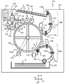
FIG. 1 shows a cross section of an
インクジェットプリンタ100は、箱型の筐体101を有している。筐体101の内部にY軸方向下部から上部に向かって、給紙カセット102、上流搬送路104a、保持ドラム105、印字部109、下流搬送路104b、排紙トレイ103を備えている。給紙カセット102はインクジェットプリンタ100で印字するための用紙Sを収容する。印字部109のインクジェットヘッド1A−1Cは、保持ドラム105上に保持された用紙Sにインク滴を吐出して画像を記録する部分である。
The
給紙カセット102は、用紙Sを収容し筐体101の下部に設けられている。給紙ローラ106は、給紙カセット102から用紙Sを一枚ずつ上流搬送路104aへ送る。上流搬送路104aは、送りローラ対115a、115bと用紙Sの搬送方向を規制する用紙案内板116で構成されている。用紙Sは、送りローラ対115a、115bの回転によって搬送され、送りローラ対115bを通過後、用紙案内板116によって保持ドラム105の外周面へ送られる。図1中の破線矢印は用紙Sの案内経路を示す。
The
保持ドラム105は、表面に薄い樹脂製の絶縁層105aを有しているアルミニウム製の円筒になっている。円筒の周長は、画像を記録する用紙Sの縦方向長さより長く、円筒の軸方向の長さは、用紙Sの横方向の長さより長くなっている。モータ118によって、一定の周速で矢印R方向に回転させている。保持ドラム105の絶縁層105aは、静電気によって用紙Sを保持しながら、回転して用紙Sを印字部109へ搬送する。絶縁層105aに静電気を帯電させる帯電ローラ108を絶縁層105aに沿って配置している。
The holding
帯電ローラ108は、金属製の回転軸を有し、回転軸周囲に導電ゴム層を有している。帯電ローラ108は、高電圧発生回路114に接続されている。導電ゴム層表面が、保持ドラム105の絶縁層105aに接し、帯電ローラ108の周速が保持ドラム105と同じ周速で回転するように、帯電ローラ108をモータで駆動している。保持ドラム105の絶縁層105aと帯電ローラ108の導電ゴム層が接して、ニップを形成する。用紙Sは、送りローラ対115b及び用紙案内板116によって、ニップへ送られる。用紙Sがニップへ搬送される直前に帯電ローラ108の金属軸に高電圧発生回路114が発生する高電圧を印加する。高電圧によって絶縁層105aは帯電し、ニップに搬送された用紙Sも帯電して保持ドラム105の外周面上に静電吸着される。静電吸着された用紙Sは、保持ドラム105の回転によって、印字部109へ送られる。
The charging
印字部109は、インクジェットヘッド1A−1Cのインク吐出面が保持ドラム105の外周面から1mm離れて、インクジェットプリンタ100に固定されている。各インクジェットヘッド1A−1Cは、保持ドラム105の軸方向(主走査方向)に長く、回転方向(副走査方向)に短い構成で、保持ドラム105の周方向に間隔を開けて配置されている。インクジェットヘッド1A−1Cは、供給されたインクの一部を画像形成のためにノズルから吐出し、残ったインクをインクジェットヘッド外へ排出する。排出されたインクを回収し、インクは、再びインクジェットヘッドへ供給される。所謂、循環型インクジェットヘッドになっている。インクジェットヘッド1A−1Cの詳細な構造は後述する。インクタンク113はシアンインク(インク)を貯留するインク容器である。インクタンク113とインクジェットヘッド1A間にインク循環装置120が配置されている。
The
インク循環装置120は、インク供給ポンプ121、供給用インクタンク122、第1圧力調整部123、回収用インクタンク124、第2圧力調整部125、インク回収ポンプ126で構成されている。インクは、画像信号に従って、インクジェットヘッド1Aから吐出される。インク供給ポンプ121は、吐出したインク量に相当するインクをインクタンク113から供給用インクタンク122へ供給する。供給用インクタンク122は、インクを貯留し、流路127を通してインクジェットヘッド1Aへ供給する。さらに、インクタンク122は、第1圧力調整部123を備えている。回収用インクタンク124は、インクジェットヘッド1Aから流路128を通して排出されたインクを貯留する。さらに、回収用インクタンク124は、第2圧力調整部125を備えている。インク回収ポンプ126は、回収用インクタンク124に貯留したインクを供給用インクタンク122へ送液する。インクジェットヘッド1Aはインク滴を重力方向(−Y方向)に吐出する。そのため待機時にインクがインクジェットヘッド1Aから漏れ出ないように、インクジェットヘッド1Aのノズル内を大気圧に対して負圧に維持する必要がある。第1圧力調整部123と第2圧力調整部125は、インクジェットヘッド1Aへ供給したインクがインクジェットヘッド1Aのノズルからインクが漏れ出ない様に、インク圧力を大気圧に対して負圧に調整する。インクのノズル内圧力は、大気圧に対して−1KPaに設定している。インクジェットヘッド1Aのマゼンタインク、インクジェットヘッド1Bのイエローインクと透明インク、インクジェットヘッド1Cのブラックインクについても、夫々同様なインクタンク113とインク循環装置120を備えている。図中では、シアンインクインク以外のインクタンク113やインク循環装置120は、省略している。
The
印字部109では、各インクジェットヘッド1A−1Cが用紙S上にインクを吐出しながら画像を記録する。記録する画像は、インクジェットプリンタ100の外部から入力された画像信号に従って描画される。インクジェットヘッド1Aはシアンインクを吐出しシアン画像とマゼンタインクを吐出しマゼンタ画像を形成する。同様に、インクジェットヘッド1Bはイエローインクと透明インクを吐出する。インクジェットヘッド1Cはブラックインクを吐出する。インクジェットヘッド1A−1Cは、各色の画像を記録するようになっている。インクジェットヘッド1A−1Cは吐出するインク色を除き同じ構造になっている。
In the
印字部109で記録が完了した用紙Sは、除電装置110、剥離爪111へ搬送される。除電装置110は、断面がコの字型に作られ、保持ドラム105の軸方向の長さと同じ長さのステンレス筐体内にタングステンワイヤーを張った構成になっている。除電装置110は、コの字型の筐体の開口が保持ドラム105の外周面に向かうよう、配置されている。高電圧発生回路117は、帯電ローラ108に印加した電圧とは逆極性の高電圧を発生する。記録が完了した用紙Sの先端が、除電装置110の下部へ搬送されると、高電圧発生回路117で発生した高電圧を筐体とタングステンワイヤー間に印加する。高電圧によって除電装置110の開口側からコロナ放電が発生し、帯電した用紙Sを除電する。剥離爪111は、爪先端が保持ドラム105の外周面に接する位置と、外周面から離間するする位置を移動できるように設けられている。通常、剥離爪111は離間する位置に保持されている。用紙Sを保持ドラム105から剥離する場合、剥離爪111の先端が保持ドラム105の外周面に接し、除電した用紙Sの先端を絶縁層105aから剥離する。用紙Sの先端を外周面から離した後、剥離爪111は外周面から離間する位置へ戻される。
The paper S for which recording has been completed by the
保持ドラム105から離れた用紙Sは、送りローラ対115cへ送られる。下流搬送路104bは、送りローラ対115c、115d、115eと用紙Sの搬送方向を規制する用紙案内板116で構成される。図中の破線矢印に沿って用紙Sは、送りローラ対115c、115d、115eによって、排紙トレイ103へ排出される。
The paper S separated from the holding
インクジェットヘッド1Aの構成を詳細に説明する。前述したようにインクジェットヘッド1B−1Cは、1Aと同じ構造になっている。
The configuration of the
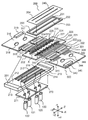
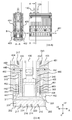
図2は、インクジェットヘッド1Aのインク吐出部200の分解斜視図である。図3は、インク吐出部200の断面図である。図4は、インク吐出部200のX部拡大図で、配線パターンを示している。図4(4−A)は、圧力室の斜視図を示している。
FIG. 2 is an exploded perspective view of the
図2に示すインク吐出部200は、ノズルプレート204、枠部材203、基板202、駆動IC(集積回路)を搭載したフィルム310、回路基板300、マニホールド201と、を備えている。
The
ノズルプレート204は、インク滴241(図3)を吐出させるノズル240を複数有している。ノズルプレート204は、ポリイミド樹脂製になっている。外形は、幅16mm(X軸方向)、長さ60mm(Z軸方向)、厚さ50μm(Y軸方向)になっている。直径20μmのノズル240が、ピッチ85μmで2本の直線状に配置されている。
The
枠部材203は、ステンレスで作成している。外形は、長さ60mm、幅16mm、厚さ1mmになっている。内側に、長さ57mm、幅6.25mmの2つの開口が形成されている。外周部は、幅1.5mmの枠になっている。幅0.5mmの仕切り壁233が、枠部材203の中央に設けられている。仕切り壁233により、二つの長方形の開口231、232が形成されている。枠部材203は、基板202とノズルプレート204間に挟まれ、インクが外部に漏れるのを防止する。開口231は、第1インク用のインク室となり、開口232は、第2インク用のインク室になる。例えば、第1インクはシアンインクであり、第2インクはマゼンタインクである。ブラックインクの場合には、開口231、232は同じブラックインク用のインク室になっている。
The
基板202は、アルミナ(Al2O3)で作られている。外形は、幅20mm、長さ60mm、厚さ1mmになっている。基板202は、第1インク供給口223、第1圧電アクチュエータ列220、第1インク排出口222、第2インク供給口227、第2圧電アクチュエータ列224、第2インク排出口226を有している。第1圧電アクチュエータ列220と第2圧電アクチュエータ列224が並置されている。枠部材203の開口232が、第1インク供給口223、第1圧電アクチュエータ列220、第1インク排出口222、を囲むように基板202上に固定されている。枠部材203の開口231が、第2インク供給口227、第2圧電アクチュエータ列224、第2インク排出口226を囲むように基板202上に固定されている。枠部材203と、第1第2圧電アクチュエータ列220、224の頂部にノズルプレート204がエポキシ接着剤で固定されている。
The
複数の第1インク供給口223と複数の第1インク排出口222が、Z軸方向に直線状に配置されている。第1圧電アクチュエータ列220は、直線状に配置された複数の第1インク供給口223と複数の第1インク排出口222の間に、配置されている。図3に示すように、基板202、仕切り壁233、ノズルプレート204、第1圧電アクチュエータ列220で囲まれた領域が、第1共通インク供給室208になる。基板202、開口232の枠部材203、ノズルプレート204、第1圧電アクチュエータ列220で囲まれた領域が、第1共通インク排出室209になる。各第1インク供給口223は、マニホールド201から第1共通インク供給室208へインクを供給する。第1共通インク室208は、第1圧電アクチュエータ列220に形成された複数の圧力室250へインクを供給する。各圧力室250の中心部にノズル240が配置されている。インクは、破線矢印で示すように、マニホールド201から、第1インク供給口223、第1共通インク供給室208、複数の圧力室250、第1共通インク排出室209、第1インク排出口222を通して、マニホールド201へ送液される。
A plurality of first
図2にもどり、複数の第2インク供給口227と複数の第2インク排出口226が、Z軸方向に直線状に配置されている。第2圧電アクチュエータ列224は、直線状に配置された複数の第2インク供給口227と複数の第2インク排出口226の間に、配置されている。図3に示すように、基板202、仕切り壁233、ノズルプレート204、第2圧電アクチュエータ列224で囲まれた領域が、第2共通インク供給室210になる。基板202、開口231の枠部材203、ノズルプレート204、第2圧電アクチュエータ列224で囲まれた領域が、第2共通インク排出室211になる。各第2インク供給口227は、マニホールド201から第2共通インク供給室210へインクを供給する。第2共通インク室210は、第2圧電アクチュエータ列224に形成された複数の圧力室251へインクを供給する。各圧力室251の中心部にノズル240が配置されている。圧力室251の容積変化によって、ノズル241からインク滴241が吐出される。インクは、破線矢印で示すように、マニホールド201から、第2インク供給口227、第2共通インク供給室210、複数の圧力室251、第2共通インク排出室211、第2インク排出口226を通して、マニホールド201へ送液される。
Returning to FIG. 2, the plurality of second
図2に示すように、マニホールド201は、基板202を固定する上面212、上面に対向する下面213を有している。基板202を固定する上面は幅20mm(X軸方向)、長さ60mm(Z軸方向)になっている。マニホールド201はアルミニウム製である。上面には4本の長溝(214、215、216、217)がZ軸方向に形成されている。マニホールド201の下面側に2つの第1接続部材270、第2接続部材271が設けられている。
As shown in FIG. 2, the manifold 201 has an
長溝214は、複数の第1インク供給口223に連通している。第1接続部材270は、長溝214と第1インク供給管129を連通させている。第1インク供給管129は、インク循環装置120に連通する流路127に接続されている。長溝215は、複数の第1インク排出口222に連通している。第1接続部材270は、長溝215と第1インク排出管130を連通させている。第1インク排出管130は、インク循環装置120に連通する流路128に接続されている。
The
長溝216は、複数の第2インク供給口227に連通している。第2接続部材271は、長溝216と第2インク供給管131を連通させている。第2インク供給管131は、インク循環装置120に連通する流路127に接続されている。長溝217は、複数の第2インク排出口226に連通している。第2接続部材271は、長溝217と第2インク排出管132を連通させている。第2インク排出管132は、インク循環装置120に連通する流路128に接続されている。第1インク供給管129と第1インク排出管130は、第1のインク用のインク循環装置120に接続されている。第2インク供給管131および第2インク排出管132は、第2のインク用のインク循環装置120に接続されている。インクジェットヘッド1Aでは、第1インク供給管129と第1インク排出管130がシアンインクに接続され、第2インク供給管131および第2インク排出管132はマゼンタインクに接続されている。インクジェットヘッド1Bでは、第1インク供給管129と第1インク排出管130がイエローインクに接続され、第2インク供給管131および第2インク排出管132は透明インクに接続されている。インクジェットヘッド1Cでは、第1インク供給管129と第1インク排出管130と、第2インク供給管131および第2インク排出管132はブラックインクに接続されている。
The
図3に示すように、マニホールド201上に、基板202、枠部材203、ノズルプレート204が、エポキシ接着剤で重ねて接着されている。枠部材203の開口232が、第1圧電アクチュエータ列220を、開口231が、第2圧電アクチュエータ列224を囲むように、基板202に固定されている。
As shown in FIG. 3, the
第1圧電アクチュエータ列220と、第2圧電アクチュエータ列224の構成を説明する。第1第2圧電アクチュエータ列220、224は同じ構成になっている。図4は、図2のX部の拡大図である。図4(4−A)は、圧電アクチュエータ(260、261)および圧力室250の斜視図である。第1、第2圧電アクチュエータ列220、224は、図4(4−A)に示す圧電アクチュエータ(260、261)および圧力室250、251が複数並んだ構成になっている。
The configuration of the first
第1、第2圧電アクチュエータ列220、224は、第1圧電体260、第2圧電体261の積層圧電体(260、261)で構成されている。第1圧電体260、第2圧電体261は、チタン酸ジルコン酸鉛(PZT)で作られている。第1圧電体260は、幅3.5mm、長さ52mm、厚さ0.9mmの大きさで、−Y方向に分極されている。第2圧電体261は、幅3.5mm、長さ52mm、厚さ0.1mmの大きさで、+Y方向に分極されている。第1圧電体260と第2圧電体261の分極方向は、逆になっている。第1圧電体260と第2圧電体261は、エポキシ接着剤で固定され、合計厚さは1mmになっている。積層圧電体(260、261)は、X軸方向の両端に、角度(θ)45度の傾斜面が形成されている。傾斜面は、Z軸方向において、一端から他端まで形成されている。結果、積層圧電体(260、261)の基板202側の幅W1は、3.5mm、ノズルプレート204側の幅W2は、1.5mmになっている。
The first and second
積層圧電体(260、261)には、傾斜面を横切るように(X軸方向)複数の溝254が形成されている。溝254の幅W3は、0.04mmになっている。溝254は、W4(0.085mm)ピッチで、等間隔にZ軸方向に配置されている。幅W5の積層圧電体(260、261)が、圧電アクチュエータとして機能する。溝254の部分が、圧力室250、251として、機能する。溝254内面に形成された電極膜221は、積層圧電体(260、261)の傾斜面および基板202表面に引出されている。第1、第2圧電アクチュエータ列220、224に形成される溝254は、図4に示すように、第1、第2圧電アクチュエータ列220、224に跨り、わずかに傾斜して設けられている。そのため、圧力室250、251の中心に設けられたノズル240、241は、Z軸方向にW6(0.085mm)ずれている。
The laminated piezoelectric body (260, 261) is formed with a plurality of grooves 254 (in the X-axis direction) so as to cross the inclined surface. The width W3 of the
第1圧電アクチュエータ列220には、圧力室250を形成する溝254が600個形成されている。各溝254の内面に電極221が形成されている。溝内の電極221は、傾斜面、および基板面上に形成された引出し電極221に繋がっている。第1圧電アクチュエータ列220に600個の圧力室250が形成されているため、600本の引出し電極221が基板202上に形成されている。同様に、第2圧電アクチュエータ列226にも、600本の引出し電極225が基板202上に形成されている。
The first
図2に示すように、第1圧電アクチュエータ列220に繋がる600本の引出電極221は、駆動IC302、313に電気的に接続されている。駆動IC302(集積回路)は直接ポリイミドフィルムの基板上に設けられている。所謂COF301(CHIP−ON−FILM)になっている。COF301のフィルムは、Z軸方向の幅25mm、X軸方向の長さ20mm、厚さ25μmのポリイミド樹脂で形成されている。COF301のフィルム上には、引出し電極221のピッチと等しいピッチで配置された電極303が形成されている。基板202上の引出し電極221とCOF301上の電極303は、異方性導電フィルム360(ACF:Anisotropic Contact Film)で電気的に接続されている(図5参照)。COF301上に設けられた電極303は300本である。300本の電極303が駆動IC302に接続されている。駆動IC302を動作させる信号線304が、COF301の電極303および駆動IC302が設けられた面上に形成されている。300本の電極303に接続する駆動IC302は、Z軸方向の長さ23mm、X軸方向の長さ2mmの長方形になっている。Y軸方向の厚さは0.5mmになっている。COF310に設けられた駆動IC313も、同様に300本の引出し電極221に接続されている。駆動IC313も、Z軸方向の長さ(長辺)23mm、X軸方向の長さ(短辺)2mmの長方形になっている。駆動IC302、313はZ軸方向に並べて配置されている。そのため、駆動IC302、313はZ軸方向に長く、X軸方向に短い形状になっている。
As shown in FIG. 2, 600
第2圧電アクチュエータ列224も、第1圧電アクチュエータ列220と同じように形成されている。第2圧電アクチュエータ列224から600本の引出し電極225が、基板202上に形成されている。600本の引出し電極225は、二つのCOF311、312の電極に接続されている。COF311、312の電極は、駆動IC314、315に接続されている。駆動IC314、315は、駆動IC302、313と同じ構成になっている。
The second
図5(5−A)は、引出電極221が形成された基板202と駆動IC302を搭載したCOF301を示している。引出電極221は溝254の内面に形成された電極へ電気的に繋がっている。引出電極221は、ACF360を通して、COF301の電極303に電気的に接続されている。電極303は、それぞれ駆動IC302のFET(Field Effect Transistor)に接続されている。二つのFETのドレインとソースが接続され、直列に配置されている。ドレインとソースの接続部に、各電極パターンが接続されている。図5(5−B)は、電極303、駆動IC302の等価回路を示している。駆動用FETは電源電圧(+Vcc、−Vcc)に接続されている。圧電アクチュエータ(260、261)は、誘電体であるPZTを二つの電極で挟む構成になっている。そのため、圧電アクチュエータ(260、261)は静電容量(C0、C1、C2、・・・Cn)として表される。圧電アクチュエータ(260、261)のC1を駆動する場合を例示する。一つの溝に形成された一つの引出電極221は、隣接する二つの圧電アクチュエータ(260、261)のC0とC1の共通電極になっている。その一つの引出電極221は、駆動IC302のFET0とFET1に接続されている。圧電アクチュエータ(260、261)のC1とC2に接続された隣接する引出電極221は、FET2とFET3に接続されている。FET0とFET3をONにして、FET2とFET1をOFFにすると、圧電アクチュエータ(260、261)のC1は剪断変形して圧力室250のインクに圧力を発生させる。FET2とFET1をONにして、FET0とFET1をOFFにすると、圧電アクチュエータ(260、261)のC1は逆向きに剪断変形して隣接する圧力室250のインクに圧力を発生させる。選択回路361は、FET0、FET1、・・・、FET2n、FET2n+1を所定のタイミングで動作させる。選択回路361と複数のFETを含む駆動IC302は、集積回路(IC)になっている。隣接する二つの圧電アクチェータ(260、261)を同時に動作させることで、圧力室255内の容積を拡張または収縮させている。圧力室250の容積変化によって、ノズル240からインク滴241を吐出させる。一つの圧力室250からインク滴を吐出させるために、6個のFETが動作する。
FIG. 5 (5-A) shows a
直線状に配置された600本の引出電極221に、COF301の300本の電極303がそれぞれ接続され、電極303が駆動IC302のFETに接続される。そのため、駆動IC302はZ軸方向に長い長方形の集積回路になっている。
The 300
図2に戻り、回路基板300を説明する。回路基板300は、インクジェットヘッド1A−1Cの外部から入力される印字用のデータに従い選択回路361を動作させる信号発生回路、FETの電源電圧(+Vcc、−Vcc)、温度検出回路などを含んでいる。また、回路基板300は、インクジェットプリンタ100からインクジェットヘッド1A−1Cへ入力される信号を受けるためのコネクタ345を搭載している。
Returning to FIG. 2, the
回路基板300は、プリント配線板340、回路部品346(図8)、コネクタ345、COF301の信号線304に接続する配線342、COF310の信号線304に接続する配線341を備えている。回路部品346は、選択回路361を動作させる信号発生回路、FETの電源電圧(+Vcc、−Vcc)、温度検出回路などを構成する。
The
プリント配線板340は、多層のガラスエポキシ基板である。プリント配線板340の外形は、Z軸方向の長さL1:55mm、X軸方向長さL2:50mm、厚さ0.8mmになっている(図6参照)。プリント配線板340の表面および内部に、銅箔で形成された回路配線が形成されている。銅箔で形成された回路配線が、回路部品346を結線している。プリント配線板340のX軸方向の一方の端部には、COF301の信号線304にACFで接続するための、接続用配線342が形成されている。同様に、COF310の信号線304に接続するための接続用配線341が、Z軸方向において接続用配線342の隣に配置されている。回路部品346によって発生した信号は、配線342、341とACFを通して、COF301、310へ送信される。プリント配線板340には、二つの直径10mmの円形の開口343、344が形成されている。開口343、344は、後述するように駆動IC302、313で発生する熱を逃がすために、設けられている。
The printed
プリント配線板316は、プリント配線板340と同じ構成になっている。プリント配線板316にも、二つの開口317、318が形成されている。開口317、318は、直径10mmの円形の貫通穴になっている。COF311、312がプリント配線板316の接続用配線に接続されている。プリント配線板316には、インクジェットプリンタ100と接続するコネクタ319が設けられている。
The printed
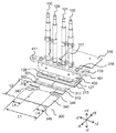
図6乃至11を参照し、インクジェットヘッド1Aの構成を説明する。図6乃至10は、インクジェットヘッド1Aを組立てる過程の展開図を示している。図11(11−A)は、インクジェットヘッド1Aの外形図を示している。図11(11−B)は、インクジェットヘッド1Aの断面図を示している。
The configuration of the
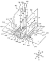
図6を参照する。固定部材400は、インク吐出部200に、第1インク供給管129、第1インク排出管130、第2インク供給管131、および第2インク排出管を、固定している。さらに、インクジェットヘッド1Aをインクジェットプリンタ100へ固定するための支持部材401が、固定部材400に固定されている。四角形の開口410、411が、支持部材401に設けられている。四角形の開口410、411を通して、インクジェットヘッド1Aは、インクジェットプリンタ100の所定の位置にねじ止めされる。固定部材400、支持部材401は、ステンレスで作成している。
See FIG. The fixing
プリント配線板340の開口343、344は、直径10mmの円形の貫通穴になっている。L3は、駆動IC302、313近傍のプリント配線板340の端部から、開口343、344の中心までの距離を示している。L3は12mmになっている。L4は、プリント配線板340のZ軸方向の両端部から、開口343、344の中心までの距離を示している。L4は13mmになっている。プリント配線板316にも、プリント配線板340と同じように、開口317、318が形成されている。開口343、344の中心は、ほぼ駆動IC302、310のZ軸方向の中心線上で、駆動IC302、310に近い位置になっている。
The
図7は、プリント配線板340、駆動IC302、313を支持する第1の熱伝導部材402を示している。第1の熱伝導部材402の外形は、概ねZ軸方向の長さL5:55mm、Y軸方向の長さL6:70mm、厚さ1.5mmになっている。第1の熱伝導部材402の材質は、純アルミニウム製である。第1の熱伝導部材402は、Z軸方向の端部に固定用のネジ穴425、426を備えている。ネジ424、427が、ネジ穴425、426を通して第1の熱伝導部材402を固定部材400に固定している。第1の熱伝導部材402には、Z軸方向の長さ55mm、Y軸方向の長さ4mmの凸平面428が形成されている。凸平面428は、第1の熱伝導部材340をエンボス加工によって形成されている。凸部の高さは0.3mmになっている。第1熱伝導部材402は、プリント配線板340を支持し、さらに、駆動IC302、312が発生する熱を伝導させる。熱伝導部材402の表面に厚さ0.05mmのPET膜(ポリエチレンテレフタレート膜)421が、固定されている。PET膜421は、プリント配線板340と純アルミニウム製の第1の熱伝導部材402を絶縁するために設けている。PET膜421は、直径10mmの開口422、423を後述するようにプリント配線板340の開口343、344に対応する位置に有している。
FIG. 7 shows a first heat
第1熱伝導部材402と第1熱伝導部材403は同じ構成になっている。第1熱伝導部材403は、凸平面428と同じ形状の凸平面432を備えている。また、第1熱伝導部材403は、直径10mmの開口449を有するPET膜を備えている。開口449は、プリント配線板316の開口317に対応する位置に設けられている。図7では省略されているが、PET膜は、プリント配線板316の開口318に対応する位置に開口450(直径10mmの開口)を有している。
The first heat
図8は、マニホールド201に沿ってCOF301、310を+Y方向に向けてほぼ直角に曲げ、プリント配線板340を第1の熱伝導部材402に沿うように固定した構成を示している。プリント配線板316も第1の熱伝導部材403に沿うように固定されている。COF301、310をほぼ直角に曲げることで、COF301,310上に設けられた駆動IC302、313の上面は、第1の熱伝導部材402の凸平面部428に接触する。駆動IC302,313を、電気的に絶縁するために、凸平面部428と駆動IC302、313の上面の間に、厚さ0.03mmのPET膜461(図12参照)を介して接触させている。PET膜461は、駆動IC302、313から凸平面428への熱移動を妨げない程度の厚さになっている。基板202に繋がるCOF301、310、311、312は、ステンレスカバー205によって覆われている。ステンレスカバー205は、厚さ0.1mmのステンレスで作成している。ステンレスカバー205は、ノズル240が形成された領域は露出するようになっている。露出部分のノズル240を通して、インク滴241が吐出される。インクジェットプリンタ100からの信号ケーブル350が、コネクタ345に挿入されている。インクジェットプリンタ100からの入力信号が信号ケーブル350を通してプリント配線板340に入力される。
FIG. 8 shows a configuration in which the
図9は、第2の熱伝導部材404、405を示している。図9では、図8で示す構成のインクジェットヘッド1Aへ第2の熱伝導部材404、405を組合わせる工程も示している。
FIG. 9 shows the second heat
第2の熱伝導部材404を説明する。第2の熱伝導部材404と405は同じ構成になっている。第2の熱伝導部材404、405は、インクジェットへド1Aの筐体にもなっている。第2の熱伝導部材は、アルミダイキャストで作成している。第2の熱伝導部材404の内面(プリント配線板316に対向する面)には、二つの円形の突起440、441が設けられている。円形突起440、441は、直径9.5mmで、第2の熱伝導部材404を第1熱伝導部材403に組み付けたときに、第1熱伝導部材403の表面に接触する高さになっている。円形突起440は、PET膜の開口450、プリント配線板316の開口318を通して、第1の熱伝導部材403に接触する。円形突起441は、PET膜の開口449、プリント配線板316の開口317を通して、第1の熱伝導部材に接触する。円形突起440、441の中心には、ネジを通す開口を備え、第1の熱伝導部材403に固定される。第2熱伝導部材404は、板バネ442を内面に備えている。第2熱伝導部材404を第1の熱伝導部材403に固定すると、板バネ442は、COF311の駆動IC314と、COF312の駆動IC315を第1の熱伝導部材403の凸平面432へ押し付ける。第2の熱伝導部材403の外面には、放熱用の突起が多数設けられている。この突起によって第2の熱伝導部材403の放熱を促している。
The second heat
第2の熱伝導部材405も、第2の熱伝導部材404と同じ構成になっている。第2の熱伝導部材404、405は、図9に示すように、ネジ443、444、451、452、453、454、455、456で第1の熱伝導部材402、403に固定している。
The second heat
図10は、上面カバー406を組み付ける工程を示している。上面カバー406は、第2の熱伝導部材404、405にネジ465、466、467、468で固定されている。固定する時に、コネクタ345に繋がる信号ケーブル350、コネクタ319に繋がる信号ケーブル(図10では省略)、第1インク供給管129、第1インク排出管130、第2インク供給管131、第2インク排出管132が、上面カバー406を通っている。組み立て後、第2の熱伝導部材404、405の境界部470、および上面カバー406と第2の熱伝導部材404、405との境界部471は、エポキシ樹脂で封止されている。
FIG. 10 shows a process of assembling the
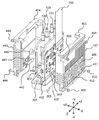
図11は、インクジェットヘッド1Aの平面図および、A−A断面図を示している。図11(11−B)は、図11のB部を拡大した図である。
FIG. 11 shows a plan view of the
図11(11−B)に示すように、第1圧電アクチュエータ列220にCOF301がACF360を介して接続されている。板バネ460によって、COF301の駆動IC302は、PET膜461を介して第1熱伝導部材402の凸平面428に圧接される。第1圧電アクチュエータ列220の動作によって発生する駆動IC302の熱は、凸平面428へ伝熱される。破線の矢印480に沿って、熱は、第1熱伝導部材402と第2熱伝導部材405の接触面481およびネジ452を通して第2熱伝導部材405に伝熱される。第2圧電アクチュエータ列224についても、同様に、破線482に沿って第1熱伝導部材403を伝熱し、接触面483を通して第2熱伝導部材404へ伝熱される。
As shown in FIG. 11 (11-B), the
金属板462は、第2熱伝導部材405とステンレスカバー205を同電位にしている。金属板447は、第2熱伝導部材404とステンレスカバー205を同電位にしている。
The
インクジェットプリンタ100に搭載するインクジェットヘッド1Aは、上述のインクジェットヘッド1Aを複数個千鳥に配列した構成になっている。千鳥配列することで、所謂ラインヘッドを形成している。ラインヘッドの印字幅は、保持ドラム105の軸方向における記録媒体Sの幅になっている。
The
この実施形態では、第1熱伝導部材402、403の材質は、純アルミニウムである。純アルミニウムの熱伝導率は、237W/(m・℃)になっている。第1熱伝導部材402,403はインクジェットヘッド1A内に収納するため、板材で高熱伝導率の純アルミニウムを使っている。第1熱伝導部材402、403に用いる他の材料として、銅(398W/(m・℃))、銀(銀420W/(m・℃))を利用可能である。第2熱伝導部材404、405は、内面に円形突起440、441を有し、かつ外面に放熱用の突起を形成するためにアルミダイキャストによって作成している。アルミダイキャスト用合金の熱伝導率は、95から138W/(m・℃)である。他のダイキャスト材料として、亜鉛合金(110W/(m・℃))やマグネシウム合金(50W/(m・℃))を利用可能である。第1熱伝導部材402、403の熱伝導率が、第2熱伝導部材404、405の熱伝導率より高くなっている。この構成により、インクジェットヘッド1A内の狭い空間内で、駆動IC302、313で発生した熱を、高効率よく第2熱伝導部材404、405に伝えることができる。
In this embodiment, the material of the first heat
駆動ICの耐熱温度は、80℃になっている。上述のように、インク滴を吐出する1つのノズルに連通する1つの圧力室からインク滴を吐出させるために、6個のFETが動作する。600個のノズル240からインク滴を連続的に吐出させ続けると、3600個のFETが連続的に動作する。また、インクジェットヘッド1Aは、密閉した構成になっている。密閉しているため、インクジェットプリンタ100で浮遊するインクミストが、インクジェットヘッド1A内に入り込むことを防止することができる。しかし、密閉しているため、インクジェットヘッド1A内で発生した熱によって、駆動IC302、313が耐熱温度を超える可能性がある。耐熱温度を超えると、駆動ICが破損する可能性がある。この実施形態の構成により、駆動ICで発生する熱をインクジェットヘッド1A内に留まらせず、効率よく放熱できるため、駆動ICの破損を防ぐことができる。なお、密閉とは、インクジェットヘッド内にミストが入り込まない程度に、第2熱伝導部材である筐体が、インク吐出部、集積回路、回路基板、第1熱伝導部材を囲んでいることを、意味している。
The heat resistant temperature of the drive IC is 80 ° C. As described above, six FETs operate to eject ink droplets from one pressure chamber communicating with one nozzle that ejects ink droplets. When the ink droplets are continuously ejected from the 600
駆動IC302、312で発生した熱は、高熱伝導率の第1熱伝導部材402、403を+Y方向に伝わり、第2熱伝導部材404、405(筐体)へ伝えられる。そのため、駆動IC302、312で発生した熱が、マニホールド201、第1インク供給管129、第1インク排出管130、第2インク供給管131、第2インク排出管132を通して、インクを加熱することを、防ぐことができる。インク温度が上がると、インクの粘度が低下する。インク粘度の低下によって、同じ圧力室の容積変化でも、吐出するインク量が増える。インク量が変化すると、印刷した画像濃度が変化する。本実施形態の構成により、画像濃度の変化を抑制可能である。
The heat generated by the
円形開口343、344の中心を、駆動IC302、313のZ軸方向の中心線上に配置している。前述したように駆動IC302、313は、Z軸方向に長く、X軸方向に短い短冊型の構成になっている。短冊形の駆動IC302、313の中心線上に、円形開口343、344の中心を配置することで、駆動IC302、313全体で発生する熱を効率よく第1熱伝導部材へ伝導させることができる。熱が第1熱伝導部材へ効率よく伝導するため、第2熱伝導部材から効率よく放熱できる。
The centers of the
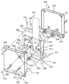
(第2の実施形態)
図12は、第2の実施形態のインクジェットヘッド1Aを示している。プリント配線板316、340に形成された開口317、318、343、344の形状が、第1の実施形態と異なっている。開口形状の差異以外は、第1の実施形態と同じである。
(Second embodiment)
FIG. 12 shows the
第2の実施形態の開口343、344は、直径10mmの半円と、その半円に連続する10mmの幅でプリント配線板340をZ軸方向の端部まで切除した形状になっている。第2熱伝導部材403の突起形状を、この開口形状に合わせることで、第1熱伝導部材402と第2熱伝導部材403の接触面積を増やすことができる。接触面積を増やすことで、より放熱し易くなる。第2の実施形態の開口317、318は、開口343、344と同じ開口形状になっている。
The
(第3の実施形態)
図13は、第3の実施形態のインクジェットヘッド1Aを示している。第2熱伝導部材501、502の構成が、第1実施形態の第2熱伝導部材404、405の構成と異なっている。第2の熱伝導部材501、502以外の構成は、第1の実施形態のインクジェットヘッド1Aと同じである。
(Third Embodiment)
FIG. 13 shows the
第2熱伝導部材501、502は厚さ0.5mmの純アルミニウムの板材で構成している。第2熱伝導部材501は、円形の熱伝導体503、504を介して、第1熱伝導部材402に接している。円形の熱伝導体503、504は、熱伝導率の高い銅でできている。第1熱伝導部材402と第2熱伝導部材501をともに純アルミニウム板で作ることで、軽量化される。第2熱伝導部材502は、円形の熱伝導体505、506を介して、第1熱伝導部材403に接している。円形の熱伝導体505、506も、銅でできている。
The second heat
上記のように、インクジェットプリンタ100は、次の構成を備えている。
筐体と、
液体を吐出する複数のノズルと、
前記ノズルに連通し、前記ノズルごとに設けられた圧力室と、
前記各圧力室に対応して設けられ、各圧力室内の液体に圧力変化を発生させる圧力発生素子と、
前記圧力室へ液体を供給する液体供給口と、
前記ノズルから吐出しなかった液体を前記圧力室から排出する液体排出口と、
前記筐体内に保持され、前記複数の圧力発生素子を駆動する集積回路と、
前記集積回路に接続され、前記集積回路を動作させる電気信号を発生する回路基板と、
前記回路基板を支持し、前記集積回路と前記筐体の内面に接触して、前記筐体に保持される熱伝導部材と、を備える液体噴射装置と、
前記液体供給口へ液体を供給し、前記排出口から吐出しなかった液体を回収し、再び液体を液体噴射装置へ供給する液体循環装置と、
前記液体噴射装置によって画像を形成する記録媒体を搬送する搬送装置と、を備える液体噴射記録装置。
As described above, the
With the housing
Multiple nozzles that discharge liquid and
A pressure chamber that communicates with the nozzle and is provided for each nozzle,
A pressure generating element provided corresponding to each of the pressure chambers and generating a pressure change in the liquid in each pressure chamber.
A liquid supply port that supplies liquid to the pressure chamber and
A liquid discharge port that discharges the liquid that was not discharged from the nozzle from the pressure chamber, and a liquid discharge port.
An integrated circuit held in the housing and driving the plurality of pressure generating elements,
A circuit board that is connected to the integrated circuit and generates an electric signal that operates the integrated circuit.
A liquid injection device that supports the circuit board and includes a heat conductive member that contacts the integrated circuit and the inner surface of the housing and is held in the housing.
A liquid circulation device that supplies a liquid to the liquid supply port, collects the liquid that has not been discharged from the discharge port, and supplies the liquid to the liquid injection device again.
A liquid injection recording device including a transport device for transporting a recording medium that forms an image by the liquid injection device.
上記実施形態では、インクジェットヘッドを例として説明した。本願のインクジェットヘッドを含む液体噴射装置は、液体分注装置や、3D印刷機の液体樹脂噴射装置としても利用可能である。 In the above embodiment, the inkjet head has been described as an example. The liquid injection device including the inkjet head of the present application can also be used as a liquid dispensing device and a liquid resin injection device for a 3D printing machine.
本発明の実施形態は、例として提示したものであり、発明の範囲を限定することは意図していない。これらの新規な実施形態は、その他の様々な形態で実施されることが可能であり、発明の要旨を逸脱しない範囲で、種々の省略、置き換え、変更を行うことができる。これらの実施形態やその変形は、発明の範囲や要旨に含まれるとともに、特許請求の範囲に記載された発明とその均等の範囲に含まれる。 The embodiments of the present invention are presented as examples and are not intended to limit the scope of the invention. These novel embodiments can be implemented in various other embodiments, and various omissions, replacements, and changes can be made without departing from the gist of the invention. These embodiments and modifications thereof are included in the scope and gist of the invention, and are also included in the scope of the invention described in the claims and the equivalent scope thereof.
1、1A、1B、1C、1D インクジェットヘッド
100 インクジェットプリンタ
120 インク循環装置
200 インク吐出部
302、313、314、315 駆動IC
301、310、311、312 COF
316、340 プリント配線板
402、403 第1熱伝導部材
404、405 第2熱伝導部材
440、441 円形突起
481、483 接触面
1, 1A, 1B, 1C,
301, 310, 311 and 312 COF
316, 340 Printed
Claims (5)
液体を吐出する複数のノズルと、
前記ノズルに連通し、前記ノズルに対応して設けられた圧力室と、
前記各圧力室に対応して設けられ、各圧力室内の液体に圧力変化を発生させる圧力発生素子と、
前記筐体内に保持され、前記複数の圧力発生素子を駆動する集積回路と、
前記集積回路に接続され、前記集積回路を動作させる電気信号を発生する回路基板と、
前記回路基板を支持し、前記集積回路と前記筐体の内面に接触して、前記筐体に保持される熱伝導部材と、
を有し、
前記筐体の前記突起部が前記回路基板に設けられる開口を通して前記熱伝導部材に接触している液体噴射装置。 A housing with protrusions on the inner surface and
Multiple nozzles that discharge liquid and
A pressure chamber that communicates with the nozzle and is provided corresponding to the nozzle,
A pressure generating element provided corresponding to each of the pressure chambers and generating a pressure change in the liquid in each pressure chamber.
An integrated circuit held in the housing and driving the plurality of pressure generating elements,
A circuit board that is connected to the integrated circuit and generates an electric signal that operates the integrated circuit.
A heat conductive member that supports the circuit board, contacts the integrated circuit and the inner surface of the housing, and is held in the housing.
Have,
A liquid injection device in which the protrusion of the housing is in contact with the heat conductive member through an opening provided in the circuit board.
前記回路基板の開口は、前記長辺の中心を通り、前記直交する方向の線上に配置されている請求項1に記載の液体噴射装置。 The integrated circuit has a long side in the arrangement direction of the plurality of pressure generating elements and a short side in a direction orthogonal to the arrangement direction.
Said circuit opening of the substrate, through the center of the long side, a liquid ejecting apparatus according to claim 1, which is arranged on a line in a direction the perpendicular.
前記集積回路で発生した熱は、前記熱伝導部材から前記突起部を通じて前記筐体に伝熱される請求項3に記載の液体噴射装置。 The protrusion of the housing comes into contact with the heat conductive member through the opening of the insulating film and the opening of the circuit board.
The liquid injection device according to claim 3 , wherein the heat generated in the integrated circuit is transferred from the heat conductive member to the housing through the protrusion.
前記熱伝導部材が前記筐体に保持されると、前記板バネによって前記集積回路が前記熱伝導部材に押し付けられる請求項4に記載の液体噴射装置。 A leaf spring is further provided on the inner surface of the housing.
The liquid injection device according to claim 4 , wherein when the heat conductive member is held in the housing, the integrated circuit is pressed against the heat conductive member by the leaf spring.
Priority Applications (3)
| Application Number | Priority Date | Filing Date | Title |
|---|---|---|---|
| JP2016229043A JP6894217B2 (en) | 2016-11-25 | 2016-11-25 | Liquid injection device |
| US15/694,927 US10232612B2 (en) | 2016-11-25 | 2017-09-04 | Liquid jetting device |
| CN201710794392.7A CN108099407B (en) | 2016-11-25 | 2017-09-05 | Liquid injection apparatus |
Applications Claiming Priority (1)
| Application Number | Priority Date | Filing Date | Title |
|---|---|---|---|
| JP2016229043A JP6894217B2 (en) | 2016-11-25 | 2016-11-25 | Liquid injection device |
Publications (2)
| Publication Number | Publication Date |
|---|---|
| JP2018083387A JP2018083387A (en) | 2018-05-31 |
| JP6894217B2 true JP6894217B2 (en) | 2021-06-30 |
Family
ID=62193073
Family Applications (1)
| Application Number | Title | Priority Date | Filing Date |
|---|---|---|---|
| JP2016229043A Active JP6894217B2 (en) | 2016-11-25 | 2016-11-25 | Liquid injection device |
Country Status (3)
| Country | Link |
|---|---|
| US (1) | US10232612B2 (en) |
| JP (1) | JP6894217B2 (en) |
| CN (1) | CN108099407B (en) |
Families Citing this family (11)
| Publication number | Priority date | Publication date | Assignee | Title |
|---|---|---|---|---|
| CN110626070B (en) * | 2018-09-19 | 2020-08-21 | 精工爱普生株式会社 | Liquid ejecting apparatus, liquid ejecting system, and print head |
| JP7151339B2 (en) * | 2018-09-28 | 2022-10-12 | 株式会社リコー | head module, head unit, Device for ejecting liquid |
| CN112549784B (en) * | 2019-09-26 | 2022-11-08 | 兄弟工业株式会社 | Heater unit, head module, and printing apparatus provided with same |
| CN114450164B (en) * | 2019-11-20 | 2023-04-25 | 株式会社御牧工程 | Ink jet printer |
| CN111613888B (en) * | 2020-06-02 | 2021-10-08 | 华中科技大学 | Integrated conformal manufacturing method of multilayer interconnected three-dimensional circuit |
| JP2022150859A (en) * | 2021-03-26 | 2022-10-07 | セイコーエプソン株式会社 | Liquid discharge device |
| JP2022150857A (en) * | 2021-03-26 | 2022-10-07 | セイコーエプソン株式会社 | Liquid discharge device |
| JP2022150858A (en) * | 2021-03-26 | 2022-10-07 | セイコーエプソン株式会社 | Liquid discharge device |
| JP2023031359A (en) * | 2021-08-25 | 2023-03-09 | 東芝テック株式会社 | Drive device and liquid discharge head |
| JP2023077738A (en) * | 2021-11-25 | 2023-06-06 | 東芝テック株式会社 | liquid ejection head |
| JP2023088371A (en) * | 2021-12-15 | 2023-06-27 | 東芝テック株式会社 | liquid ejection head |
Family Cites Families (16)
| Publication number | Priority date | Publication date | Assignee | Title |
|---|---|---|---|---|
| DE3115017A1 (en) * | 1981-04-14 | 1982-11-04 | Blaupunkt-Werke Gmbh, 3200 Hildesheim | Electronic components |
| IL134659A (en) * | 1997-08-22 | 2003-01-12 | Xaar Technology Ltd | Method of manufacture of printing apparatus |
| JP4228632B2 (en) * | 2002-08-30 | 2009-02-25 | コニカミノルタホールディングス株式会社 | Inkjet head and inkjet printer |
| US7360870B2 (en) * | 2004-02-24 | 2008-04-22 | Brother Kogyo Kabushiki Kaisha | Nozzle plate for high-resolution inkjet print head |
| JP4569151B2 (en) * | 2004-03-31 | 2010-10-27 | ブラザー工業株式会社 | Inkjet printer head unit, inkjet printer, and signal transmission board used therefor |
| JP4616609B2 (en) * | 2004-10-05 | 2011-01-19 | ブラザー工業株式会社 | Inkjet head |
| WO2007015230A2 (en) * | 2005-08-04 | 2007-02-08 | Hewlett-Packard Industrial Printing Ltd. | A method of cooling and servicing an inkjet print head array |
| JP4770400B2 (en) * | 2005-11-01 | 2011-09-14 | ブラザー工業株式会社 | Inkjet recording device |
| CN101106893B (en) * | 2007-08-01 | 2010-05-26 | 锐德科无线通信技术(上海)有限公司 | Printed circuit board with heat dispersion structure |
| JP5367629B2 (en) * | 2010-03-30 | 2013-12-11 | 理想科学工業株式会社 | Inkjet printer |
| JP2012125936A (en) * | 2010-12-13 | 2012-07-05 | Toshiba Tec Corp | Inkjet head |
| CN104135814A (en) * | 2013-05-02 | 2014-11-05 | 鸿富锦精密工业(深圳)有限公司 | Printed circuit board |
| JP6390207B2 (en) * | 2013-08-30 | 2018-09-19 | セイコーエプソン株式会社 | Liquid ejection device, print head unit, and drive substrate |
| US9209141B2 (en) * | 2014-02-26 | 2015-12-08 | International Business Machines Corporation | Shielded package assemblies with integrated capacitor |
| JP6306991B2 (en) * | 2014-09-19 | 2018-04-04 | 株式会社東芝 | Inkjet head and printer |
| JP6848246B2 (en) * | 2016-07-27 | 2021-03-24 | ブラザー工業株式会社 | Liquid discharge head |
-
2016
- 2016-11-25 JP JP2016229043A patent/JP6894217B2/en active Active
-
2017
- 2017-09-04 US US15/694,927 patent/US10232612B2/en active Active
- 2017-09-05 CN CN201710794392.7A patent/CN108099407B/en active Active
Also Published As
| Publication number | Publication date |
|---|---|
| CN108099407A (en) | 2018-06-01 |
| CN108099407B (en) | 2019-11-19 |
| US10232612B2 (en) | 2019-03-19 |
| JP2018083387A (en) | 2018-05-31 |
| US20180147845A1 (en) | 2018-05-31 |
Similar Documents
| Publication | Publication Date | Title |
|---|---|---|
| JP6894217B2 (en) | Liquid injection device | |
| US9751305B2 (en) | Liquid discharge head and recording device using the same | |
| JP5944571B2 (en) | Liquid discharge head and recording apparatus including the same | |
| US9365039B2 (en) | Liquid jet head, method for manufacturing liquid jet head, and liquid jet apparatus | |
| JP6869675B2 (en) | Inkjet head and manufacturing method of inkjet head | |
| JP6869673B2 (en) | Inkjet head | |
| US11192365B1 (en) | Piezoelectric printhead and printing system | |
| JP2017213845A (en) | Liquid jet head and liquid jet device | |
| CN111204127B (en) | Liquid discharge head and liquid discharge apparatus | |
| JP6928186B2 (en) | Liquid discharge head and recording device | |
| US20180072052A1 (en) | Ink jet head | |
| US11845275B2 (en) | Liquid discharge head | |
| JP2023074110A (en) | Driving device and liquid discharge head | |
| JP2021181184A (en) | Liquid discharge head and liquid discharge device | |
| US20200023643A1 (en) | Liquid Ejecting Apparatus And Liquid Ejecting Head | |
| JP2020082492A (en) | Inkjet head and inkjet device | |
| JP2022177434A (en) | Liquid jet head and liquid jet device | |
| CN115366540A (en) | Liquid ejecting head and liquid ejecting apparatus | |
| JP2015171791A (en) | Liquid discharge device and liquid discharge head | |
| JP2010201673A (en) | Liquid jetting head and liquid jetting apparatus | |
| JP2010201753A (en) | Liquid jetting head and liquid jetting apparatus |
Legal Events
| Date | Code | Title | Description |
|---|---|---|---|
| A621 | Written request for application examination |
Free format text: JAPANESE INTERMEDIATE CODE: A621 Effective date: 20190925 |
|
| A977 | Report on retrieval |
Free format text: JAPANESE INTERMEDIATE CODE: A971007 Effective date: 20200804 |
|
| A131 | Notification of reasons for refusal |
Free format text: JAPANESE INTERMEDIATE CODE: A131 Effective date: 20200928 |
|
| A521 | Request for written amendment filed |
Free format text: JAPANESE INTERMEDIATE CODE: A523 Effective date: 20201118 |
|
| A131 | Notification of reasons for refusal |
Free format text: JAPANESE INTERMEDIATE CODE: A131 Effective date: 20210405 |
|
| A521 | Request for written amendment filed |
Free format text: JAPANESE INTERMEDIATE CODE: A523 Effective date: 20210512 |
|
| TRDD | Decision of grant or rejection written | ||
| A01 | Written decision to grant a patent or to grant a registration (utility model) |
Free format text: JAPANESE INTERMEDIATE CODE: A01 Effective date: 20210524 |
|
| A61 | First payment of annual fees (during grant procedure) |
Free format text: JAPANESE INTERMEDIATE CODE: A61 Effective date: 20210603 |
|
| R150 | Certificate of patent or registration of utility model |
Ref document number: 6894217 Country of ref document: JP Free format text: JAPANESE INTERMEDIATE CODE: R150 |