JP6885877B2 - グレーデッド拡散体 - Google Patents
グレーデッド拡散体 Download PDFInfo
- Publication number
- JP6885877B2 JP6885877B2 JP2017555230A JP2017555230A JP6885877B2 JP 6885877 B2 JP6885877 B2 JP 6885877B2 JP 2017555230 A JP2017555230 A JP 2017555230A JP 2017555230 A JP2017555230 A JP 2017555230A JP 6885877 B2 JP6885877 B2 JP 6885877B2
- Authority
- JP
- Japan
- Prior art keywords
- haze
- structured
- diffuser
- main surface
- optical
- Prior art date
- Legal status (The legal status is an assumption and is not a legal conclusion. Google has not performed a legal analysis and makes no representation as to the accuracy of the status listed.)
- Active
Links
Images


Classifications
-
- G—PHYSICS
- G02—OPTICS
- G02B—OPTICAL ELEMENTS, SYSTEMS OR APPARATUS
- G02B5/00—Optical elements other than lenses
- G02B5/02—Diffusing elements; Afocal elements
-
- G—PHYSICS
- G02—OPTICS
- G02B—OPTICAL ELEMENTS, SYSTEMS OR APPARATUS
- G02B5/00—Optical elements other than lenses
- G02B5/02—Diffusing elements; Afocal elements
- G02B5/0205—Diffusing elements; Afocal elements characterised by the diffusing properties
- G02B5/021—Diffusing elements; Afocal elements characterised by the diffusing properties the diffusion taking place at the element's surface, e.g. by means of surface roughening or microprismatic structures
- G02B5/0221—Diffusing elements; Afocal elements characterised by the diffusing properties the diffusion taking place at the element's surface, e.g. by means of surface roughening or microprismatic structures the surface having an irregular structure
-
- C—CHEMISTRY; METALLURGY
- C25—ELECTROLYTIC OR ELECTROPHORETIC PROCESSES; APPARATUS THEREFOR
- C25D—PROCESSES FOR THE ELECTROLYTIC OR ELECTROPHORETIC PRODUCTION OF COATINGS; ELECTROFORMING; APPARATUS THEREFOR
- C25D3/00—Electroplating: Baths therefor
- C25D3/02—Electroplating: Baths therefor from solutions
- C25D3/04—Electroplating: Baths therefor from solutions of chromium
-
- C—CHEMISTRY; METALLURGY
- C25—ELECTROLYTIC OR ELECTROPHORETIC PROCESSES; APPARATUS THEREFOR
- C25D—PROCESSES FOR THE ELECTROLYTIC OR ELECTROPHORETIC PRODUCTION OF COATINGS; ELECTROFORMING; APPARATUS THEREFOR
- C25D3/00—Electroplating: Baths therefor
- C25D3/02—Electroplating: Baths therefor from solutions
- C25D3/38—Electroplating: Baths therefor from solutions of copper
-
- C—CHEMISTRY; METALLURGY
- C25—ELECTROLYTIC OR ELECTROPHORETIC PROCESSES; APPARATUS THEREFOR
- C25D—PROCESSES FOR THE ELECTROLYTIC OR ELECTROPHORETIC PRODUCTION OF COATINGS; ELECTROFORMING; APPARATUS THEREFOR
- C25D5/00—Electroplating characterised by the process; Pretreatment or after-treatment of workpieces
- C25D5/10—Electroplating with more than one layer of the same or of different metals
- C25D5/12—Electroplating with more than one layer of the same or of different metals at least one layer being of nickel or chromium
-
- C—CHEMISTRY; METALLURGY
- C25—ELECTROLYTIC OR ELECTROPHORETIC PROCESSES; APPARATUS THEREFOR
- C25D—PROCESSES FOR THE ELECTROLYTIC OR ELECTROPHORETIC PRODUCTION OF COATINGS; ELECTROFORMING; APPARATUS THEREFOR
- C25D5/00—Electroplating characterised by the process; Pretreatment or after-treatment of workpieces
- C25D5/60—Electroplating characterised by the structure or texture of the layers
- C25D5/605—Surface topography of the layers, e.g. rough, dendritic or nodular layers
-
- C—CHEMISTRY; METALLURGY
- C25—ELECTROLYTIC OR ELECTROPHORETIC PROCESSES; APPARATUS THEREFOR
- C25D—PROCESSES FOR THE ELECTROLYTIC OR ELECTROPHORETIC PRODUCTION OF COATINGS; ELECTROFORMING; APPARATUS THEREFOR
- C25D7/00—Electroplating characterised by the article coated
-
- G—PHYSICS
- G02—OPTICS
- G02B—OPTICAL ELEMENTS, SYSTEMS OR APPARATUS
- G02B1/00—Optical elements characterised by the material of which they are made; Optical coatings for optical elements
- G02B1/10—Optical coatings produced by application to, or surface treatment of, optical elements
- G02B1/11—Anti-reflection coatings
- G02B1/113—Anti-reflection coatings using inorganic layer materials only
- G02B1/115—Multilayers
-
- G—PHYSICS
- G02—OPTICS
- G02B—OPTICAL ELEMENTS, SYSTEMS OR APPARATUS
- G02B1/00—Optical elements characterised by the material of which they are made; Optical coatings for optical elements
- G02B1/10—Optical coatings produced by application to, or surface treatment of, optical elements
- G02B1/14—Protective coatings, e.g. hard coatings
-
- G—PHYSICS
- G02—OPTICS
- G02B—OPTICAL ELEMENTS, SYSTEMS OR APPARATUS
- G02B3/00—Simple or compound lenses
- G02B3/0006—Arrays
- G02B3/0037—Arrays characterized by the distribution or form of lenses
- G02B3/005—Arrays characterized by the distribution or form of lenses arranged along a single direction only, e.g. lenticular sheets
-
- G—PHYSICS
- G02—OPTICS
- G02B—OPTICAL ELEMENTS, SYSTEMS OR APPARATUS
- G02B3/00—Simple or compound lenses
- G02B3/0006—Arrays
- G02B3/0037—Arrays characterized by the distribution or form of lenses
- G02B3/0062—Stacked lens arrays, i.e. refractive surfaces arranged in at least two planes, without structurally separate optical elements in-between
-
- G—PHYSICS
- G02—OPTICS
- G02B—OPTICAL ELEMENTS, SYSTEMS OR APPARATUS
- G02B5/00—Optical elements other than lenses
- G02B5/02—Diffusing elements; Afocal elements
- G02B5/0205—Diffusing elements; Afocal elements characterised by the diffusing properties
- G02B5/0236—Diffusing elements; Afocal elements characterised by the diffusing properties the diffusion taking place within the volume of the element
- G02B5/0242—Diffusing elements; Afocal elements characterised by the diffusing properties the diffusion taking place within the volume of the element by means of dispersed particles
-
- G—PHYSICS
- G02—OPTICS
- G02B—OPTICAL ELEMENTS, SYSTEMS OR APPARATUS
- G02B5/00—Optical elements other than lenses
- G02B5/02—Diffusing elements; Afocal elements
- G02B5/0205—Diffusing elements; Afocal elements characterised by the diffusing properties
- G02B5/0263—Diffusing elements; Afocal elements characterised by the diffusing properties with positional variation of the diffusing properties, e.g. gradient or patterned diffuser
-
- G—PHYSICS
- G02—OPTICS
- G02B—OPTICAL ELEMENTS, SYSTEMS OR APPARATUS
- G02B5/00—Optical elements other than lenses
- G02B5/02—Diffusing elements; Afocal elements
- G02B5/0268—Diffusing elements; Afocal elements characterized by the fabrication or manufacturing method
-
- G—PHYSICS
- G02—OPTICS
- G02B—OPTICAL ELEMENTS, SYSTEMS OR APPARATUS
- G02B5/00—Optical elements other than lenses
- G02B5/02—Diffusing elements; Afocal elements
- G02B5/0273—Diffusing elements; Afocal elements characterized by the use
- G02B5/0278—Diffusing elements; Afocal elements characterized by the use used in transmission
-
- G—PHYSICS
- G02—OPTICS
- G02B—OPTICAL ELEMENTS, SYSTEMS OR APPARATUS
- G02B5/00—Optical elements other than lenses
- G02B5/02—Diffusing elements; Afocal elements
- G02B5/0273—Diffusing elements; Afocal elements characterized by the use
- G02B5/0284—Diffusing elements; Afocal elements characterized by the use used in reflection
-
- G—PHYSICS
- G02—OPTICS
- G02B—OPTICAL ELEMENTS, SYSTEMS OR APPARATUS
- G02B6/00—Light guides; Structural details of arrangements comprising light guides and other optical elements, e.g. couplings
- G02B6/0001—Light guides; Structural details of arrangements comprising light guides and other optical elements, e.g. couplings specially adapted for lighting devices or systems
- G02B6/0011—Light guides; Structural details of arrangements comprising light guides and other optical elements, e.g. couplings specially adapted for lighting devices or systems the light guides being planar or of plate-like form
- G02B6/0033—Means for improving the coupling-out of light from the light guide
- G02B6/005—Means for improving the coupling-out of light from the light guide provided by one optical element, or plurality thereof, placed on the light output side of the light guide
- G02B6/0051—Diffusing sheet or layer
-
- G—PHYSICS
- G02—OPTICS
- G02B—OPTICAL ELEMENTS, SYSTEMS OR APPARATUS
- G02B6/00—Light guides; Structural details of arrangements comprising light guides and other optical elements, e.g. couplings
- G02B6/0001—Light guides; Structural details of arrangements comprising light guides and other optical elements, e.g. couplings specially adapted for lighting devices or systems
- G02B6/0011—Light guides; Structural details of arrangements comprising light guides and other optical elements, e.g. couplings specially adapted for lighting devices or systems the light guides being planar or of plate-like form
- G02B6/0033—Means for improving the coupling-out of light from the light guide
- G02B6/0058—Means for improving the coupling-out of light from the light guide varying in density, size, shape or depth along the light guide
- G02B6/0061—Means for improving the coupling-out of light from the light guide varying in density, size, shape or depth along the light guide to provide homogeneous light output intensity
-
- G—PHYSICS
- G02—OPTICS
- G02B—OPTICAL ELEMENTS, SYSTEMS OR APPARATUS
- G02B6/00—Light guides; Structural details of arrangements comprising light guides and other optical elements, e.g. couplings
- G02B6/0001—Light guides; Structural details of arrangements comprising light guides and other optical elements, e.g. couplings specially adapted for lighting devices or systems
- G02B6/0011—Light guides; Structural details of arrangements comprising light guides and other optical elements, e.g. couplings specially adapted for lighting devices or systems the light guides being planar or of plate-like form
- G02B6/0075—Arrangements of multiple light guides
- G02B6/0076—Stacked arrangements of multiple light guides of the same or different cross-sectional area
-
- G—PHYSICS
- G02—OPTICS
- G02F—OPTICAL DEVICES OR ARRANGEMENTS FOR THE CONTROL OF LIGHT BY MODIFICATION OF THE OPTICAL PROPERTIES OF THE MEDIA OF THE ELEMENTS INVOLVED THEREIN; NON-LINEAR OPTICS; FREQUENCY-CHANGING OF LIGHT; OPTICAL LOGIC ELEMENTS; OPTICAL ANALOGUE/DIGITAL CONVERTERS
- G02F1/00—Devices or arrangements for the control of the intensity, colour, phase, polarisation or direction of light arriving from an independent light source, e.g. switching, gating or modulating; Non-linear optics
- G02F1/01—Devices or arrangements for the control of the intensity, colour, phase, polarisation or direction of light arriving from an independent light source, e.g. switching, gating or modulating; Non-linear optics for the control of the intensity, phase, polarisation or colour
- G02F1/13—Devices or arrangements for the control of the intensity, colour, phase, polarisation or direction of light arriving from an independent light source, e.g. switching, gating or modulating; Non-linear optics for the control of the intensity, phase, polarisation or colour based on liquid crystals, e.g. single liquid crystal display cells
- G02F1/133—Constructional arrangements; Operation of liquid crystal cells; Circuit arrangements
- G02F1/1333—Constructional arrangements; Manufacturing methods
- G02F1/1335—Structural association of cells with optical devices, e.g. polarisers or reflectors
- G02F1/1336—Illuminating devices
- G02F1/133602—Direct backlight
- G02F1/133603—Direct backlight with LEDs
-
- G—PHYSICS
- G02—OPTICS
- G02F—OPTICAL DEVICES OR ARRANGEMENTS FOR THE CONTROL OF LIGHT BY MODIFICATION OF THE OPTICAL PROPERTIES OF THE MEDIA OF THE ELEMENTS INVOLVED THEREIN; NON-LINEAR OPTICS; FREQUENCY-CHANGING OF LIGHT; OPTICAL LOGIC ELEMENTS; OPTICAL ANALOGUE/DIGITAL CONVERTERS
- G02F1/00—Devices or arrangements for the control of the intensity, colour, phase, polarisation or direction of light arriving from an independent light source, e.g. switching, gating or modulating; Non-linear optics
- G02F1/01—Devices or arrangements for the control of the intensity, colour, phase, polarisation or direction of light arriving from an independent light source, e.g. switching, gating or modulating; Non-linear optics for the control of the intensity, phase, polarisation or colour
- G02F1/13—Devices or arrangements for the control of the intensity, colour, phase, polarisation or direction of light arriving from an independent light source, e.g. switching, gating or modulating; Non-linear optics for the control of the intensity, phase, polarisation or colour based on liquid crystals, e.g. single liquid crystal display cells
- G02F1/133—Constructional arrangements; Operation of liquid crystal cells; Circuit arrangements
- G02F1/1333—Constructional arrangements; Manufacturing methods
- G02F1/1335—Structural association of cells with optical devices, e.g. polarisers or reflectors
- G02F1/1336—Illuminating devices
- G02F1/133602—Direct backlight
- G02F1/133606—Direct backlight including a specially adapted diffusing, scattering or light controlling members
-
- G—PHYSICS
- G02—OPTICS
- G02B—OPTICAL ELEMENTS, SYSTEMS OR APPARATUS
- G02B5/00—Optical elements other than lenses
- G02B5/04—Prisms
-
- G—PHYSICS
- G02—OPTICS
- G02B—OPTICAL ELEMENTS, SYSTEMS OR APPARATUS
- G02B6/00—Light guides; Structural details of arrangements comprising light guides and other optical elements, e.g. couplings
- G02B6/0001—Light guides; Structural details of arrangements comprising light guides and other optical elements, e.g. couplings specially adapted for lighting devices or systems
- G02B6/0011—Light guides; Structural details of arrangements comprising light guides and other optical elements, e.g. couplings specially adapted for lighting devices or systems the light guides being planar or of plate-like form
- G02B6/0033—Means for improving the coupling-out of light from the light guide
- G02B6/005—Means for improving the coupling-out of light from the light guide provided by one optical element, or plurality thereof, placed on the light output side of the light guide
- G02B6/0053—Prismatic sheet or layer; Brightness enhancement element, sheet or layer
-
- G—PHYSICS
- G02—OPTICS
- G02F—OPTICAL DEVICES OR ARRANGEMENTS FOR THE CONTROL OF LIGHT BY MODIFICATION OF THE OPTICAL PROPERTIES OF THE MEDIA OF THE ELEMENTS INVOLVED THEREIN; NON-LINEAR OPTICS; FREQUENCY-CHANGING OF LIGHT; OPTICAL LOGIC ELEMENTS; OPTICAL ANALOGUE/DIGITAL CONVERTERS
- G02F1/00—Devices or arrangements for the control of the intensity, colour, phase, polarisation or direction of light arriving from an independent light source, e.g. switching, gating or modulating; Non-linear optics
- G02F1/01—Devices or arrangements for the control of the intensity, colour, phase, polarisation or direction of light arriving from an independent light source, e.g. switching, gating or modulating; Non-linear optics for the control of the intensity, phase, polarisation or colour
- G02F1/13—Devices or arrangements for the control of the intensity, colour, phase, polarisation or direction of light arriving from an independent light source, e.g. switching, gating or modulating; Non-linear optics for the control of the intensity, phase, polarisation or colour based on liquid crystals, e.g. single liquid crystal display cells
- G02F1/133—Constructional arrangements; Operation of liquid crystal cells; Circuit arrangements
- G02F1/1333—Constructional arrangements; Manufacturing methods
- G02F1/1335—Structural association of cells with optical devices, e.g. polarisers or reflectors
- G02F1/1336—Illuminating devices
- G02F1/133602—Direct backlight
- G02F1/133606—Direct backlight including a specially adapted diffusing, scattering or light controlling members
- G02F1/133607—Direct backlight including a specially adapted diffusing, scattering or light controlling members the light controlling member including light directing or refracting elements, e.g. prisms or lenses
Description
構造化下面の第1のエッジに沿う第1の部分と、第1の部分から構造化下面の反対側にある第2のエッジまで延在する第2の部分とを有する構造化下面であって、第2の部分は、第2の部分にわたる略一様な第2の光学ヘーズを有し、第1の部分の少なくとも一部の領域が、第1の光学ヘーズ以上の第3の光学ヘーズを有し、第2の光学ヘーズは、第1の光学ヘーズよりも低い、構造化下面とを含む。
Hm>H1>H2となる。
1.曲率の定義:(a)g曲率は、勾配方向に沿う曲率である。(b)t曲率は、勾配方向と交差する(垂直な)方向に沿う曲率である。(c)g曲率は、勾配に沿う3つの点を用いて3つの点に外接する円を計算することによって計算される。g曲率=1/R、ここで、Rは、この円の半径である。(d)t曲率は、勾配と交差する方向に沿う3つの点を用いて3つの点に外接する円を計算することによって計算される。g曲率=1/R、ここで、Rは、この円の半径である。(e)曲率は、それらの3つの点の中心点に割り当てられる。(f)3つの点の間隔は、着目していない微細な特徴による寄与を抑制するほど十分に大きいが、着目した特徴による寄与を保つほど十分に小さくなるように選ばれる。
2.リッジ上の点の曲率は、2つの垂直方向の間で十分に異なる。(a)g曲率とt曲率は、少なくとも2倍だけ異なる(いずれかがより大きくなりうる)。
3.リッジは、谷の大部分よりも鋭っている。(a)曲率は、g曲率分布の1パーセンタイル点の絶対値よりも大きい(g曲率の1%が、1パーセンタイル点よりも小さい)。
4.傾斜は、平均傾斜よりも小さい。(a)リッジ上のg傾斜(勾配に沿う傾斜)が、表面の平均g傾斜よりも小さい。(b)リッジの上部の傾斜は、非常に傾斜した表面上にない限り、典型的に略ゼロである。
5.リッジは、十分に長い。(a)潜在的なリッジは、その全長(分岐を含む)が、潜在的なリッジ上部に沿う平均曲率半径よりも小さい場合には、リッジとみなされない。(b)潜在的なリッジは、その全長が潜在的なリッジの平均幅の3分の1よりも小さい場合には、リッジとみなされない。(c)これらの寸法が概略測定されることに留意されたい。
6.分岐は、十分に長い。(a)リッジの中央セクションからの分岐は、リッジの平均幅の1.5倍よりも大きい場合には、リッジの連続部とみなされる。そうでなければ、分岐は除去される。(b)これらの寸法が概略測定されることに留意されたい。
ピーク率=A/(A+B)。

光学フィルム1802は、図17に示す光学フィルムと同様に、マイクロ構造1812を有する構造化上面1810と、第1の面1822及び第2の面1824を伴うマイクロ構造を有する構造化下面1820とを含む。光学フィルム1802は、例えば、反射偏光子、又は反射偏光子と1/4波長層若しくは1/4波長プレートとの組合せでありうる中間層1830も含む。図18の中間層1830は、簡略化されており、それ自体が、1/4波長プレートと線形反射偏光子の両方を表してもよいが、それらは、別個の層として取り扱われてもよい。光学フィルム1802は、モノリシック層でもよく、又はいくつかの積層部分又は層により形成されてもよい。
本明細書で説明する多層光学フィルム反射偏光子と同様に、多層光学フィルム反射体は、注意深く選択され、配向されると複屈折を創り出しうる、ポリマー材料の交互する高屈折率層と低屈折率層を含む。層は、共押出しされ、強め合う干渉により広域の光スペクトルが層間の界面で反射するように配向される。各層対の光学厚さは、異なる層対が、異なる波長の光の反射に寄与するように設計される。例示的な多層光学フィルム反射体は、Enhanced Specular ReflectorすなわちESR(ミネソタ州St.Paulにある3M Companyから入手可能)である。好適な反射体は、光のうち少なくとも90%、95%、98%、又は99%さえ反射することができる。反射体は、拡散面(又は均等拡散面)、鏡面、又は半鏡面として特徴付けられる反射パターンを提供することができる。
グレーデッド拡散体フィルムを以下のように作製した。110°の頂角を有するダイヤモンドを伴う刻装器を用いて、電気メッキされたシリンダ状のマイクロ複製ツールを切削して、ツールの周縁で深さが変化する六角形状の一組の凹みを生成した。ここで、ツール内のダイヤモンド切削が深いほど、ツールの多くの表面積が影響を受け、切削が浅いほど、ツールの少ない表面積が影響を受けた。ツール上の最初の10mmの六角形状の凹みが最も深かった。周縁の次の13mm〜約23mmについては、深さが単調に減少した。10mm〜約17mmは、凡そ三次スプラインに対応するプロファイルに従って深さが減少した。約17mm〜約23mmは、ツールの周縁に連続する一定の深さまで深さが線形に変化した。このようにして、平行な複数の周縁切削を行った。
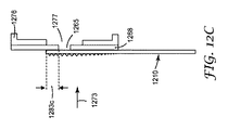
ヘーズへの上面による寄与を排除するために、「エッジグレーデッド拡散体フィルム」で説明した一様に拡散するフィルムの上面を、上部構造の屈折率に近い屈折率を有する樹脂でコーティングした。得られたフィルムを評価して、フィルムの下側の各セグメントと関連するヘーズを決定した。測定装置を図12A〜図12Cに示している。Enhanced Specular Reflector(ESR)フィルム1268(ミネソタ州St.Paulにある3M Co.から入手可能)を用いて作り出された2mmスリット1265を有する構造上にフィルム1210を配置して、ヘーズメーターの部分1276にあるヘーズメーター計測装置の開口1277(凡そ1インチ(2.54cm)の直径を有する)を覆って上部分及び下部分を隠した。下部構造のサイズのグレーディングがスリットのエッジと垂直に走るように、フィルムを配向した。ヘーズの測定値が1ミリメートル毎に取られるたびに、フィルムをスリットにわたって段階的に移動させた。図12Aでは、フィルム1210のエッジが、スリット1265のエッジと位置合わせされている。図12Bでは、フィルム1210は、約1mmの距離1283bだけシフトされており、図12Cでは、フィルム1210は、約2mmの距離1283cだけシフトされている。Haze Gard Plusヘーズメーターを用いて、スリットの上にあるフィルムセグメントのヘーズを測定した。ヘーズメーターは、図12A〜図12Cに示すような方向1273を有する入射光を発生した。図13は、フィルムにわたる位置に応じたヘーズを示している。フィルムの左端部分のヘーズは、100%に近かった。フィルムの左エッジから10mmのところでマイクロ構造の高さが減少し始めるので、ヘーズは、100%近から10%未満まで低下した。
図14A〜図14Bに例示する装置を組み立てて、「エッジグレーデッド拡散体フィルム」で説明したフィルム1210についてLEDホットスポットの光学拡散をテストした。市販されているエッジ照明型スマートフォンから、フレックス回路基板1442上にある光ガイド1404と、関連する12個のLED1440の組とを取り外した。米国特許出願公開第2013/0004728号(Boyd等)で説明される種類の2つの交差プリズムフィルムからなる層1420を、サイズが変化するマイクロ構造を伴う側面とは反対側にある、フィルムの一様な上部拡散面に、取り付けずに配した。変化するマイクロ構造を有する側面が、光ガイドに面するともに、最大の構造を伴うエッジが、LED1440の列と平行となり、LED1440の列に最も近くなるように配向された状態で、得られたフィルムを光ガイドに配置した。LEDに取り付けられたフレックス回路基板1442は、光ガイドの上に部分的に延在した。光ガイドの上方約42cm、光ガイドのうちフレックスプレートが終端する領域1455の直上に配置したPrometric PM−1613F−1撮像光度計1492(英国Milton KeynesにあるPro−Lite Technologyから入手可能)を用いて、ホットスポット測定値を取った。フレックスプレートが終端する接合部に沿ってフィルム1210を1度に1ミリメートルずつ段階的に移動させながら、1ミリメートル毎に測定値を取った。図14Aには、LED1440の最も近くのフィルム1210の端部が層1420の端部と位置合わせされるゼロ位置を例示している。図14Bは、距離1483bだけ変位されたフィルム1210を示している。図15には、フィルムのエッジからの距離に応じたホットスポットコントラスト(独立した各測定領域にわたる輝度の谷の振幅に対する輝度の山の振幅の比率として定義される)を示している。上側の拡散フィルムと下側の拡散フィルムとのこの組合せを有する市販のスマートフォンでは、コントラスト比率1.8未満の値によって、ホットスポットの許容可能な抑制がもたらされることが判明した。
国際公開第2014/081693号(Pham等)で説明されるような構造化拡散体フィルムを作製した。構造化面は、本説明の拡散体の第1の主面として用いるのに適していた。表面を、原子間力顕微鏡により特徴付け、表面傾斜の分布を決定するために分析した。表面の相補的累積傾斜分布(FCC)を図16に示している。相補的累積傾斜分布関数については、例えば、米国特許出願公開第2012/0064296号(Walker等)で説明されており、同文献は、本説明と矛盾しない範囲で参照により本明細書に組み込まれる。x軸上の各傾斜値について、y値は、その値よりも大きい傾斜の部分を示している。
第1のフーリエパワースペクトルが、
ゼロ周波数に対応せず、第1の基準線を定義する隣り合う2つの谷内に留まる1つ以上の第1の周波数ピークを含む限り、そのような任意の第1の周波数ピークが、0.8よりも小さい第1のピーク率を有し、第1のピーク率が、第1の周波数ピークと第1の基準線との間にあるエリアを第1の周波数ピークの真下のエリアにより割った値に等しく、かつ、
第2のフーリエパワースペクトルが、
ゼロ周波数に対応せず、第2の基準線を定義する隣り合う2つの谷内に留まる1つ以上の第2の周波数ピークを含む限り、そのような任意の第2の周波数ピークが、0.8よりも小さい第2のピーク率を有し、第2のピーク率が、第2の周波数ピークと第2の基準線との間にあるエリアを第2の周波数ピークの真下のエリアで割った値に等しい。
入力エッジ及び出力主面を有する光ガイドと、
実施形態1の拡散体であって、拡散体の第2の主面が光ガイドの出力主面に面し、拡散体のエッジが光ガイドの入力エッジの隣になるように、光ガイドに近接して配置された拡散体と
を備えるディスプレイである。
第1の構造化面を有する第1のマイクロ複製ツールを用意することと、
対向する第1の側面及び第2の側面を有する基材を用意することと、
第1のマイクロ複製ツールを用いて、基材の第1の側面に拡散体の第1の主面を形成することとを含み、
第1のマイクロ複製ツールを用意するステップは、
第1の電気メッキ処理により金属を電気溶着することによって金属の第1の層を形成し、第1の平均粗度を有する第1の層の第1の主面を生じさせることと、
第2の電気メッキ処理により第1の主面に金属を電気溶着することによって第1の主面に金属の第2の層を形成し、第1の平均粗度よりも小さい第2の平均粗度を有する第2の層の第2の主面を生じさせることと
を含む方法である。
第1の構造化面を有する第1のマイクロ複製ツールを用意することであって、
第1の構造化面は、表面構造の略一様な分布を有する、ことと、
対向する第1の主面及び第2の主面を有する基材を用意することと、
第1のマイクロ複製ツールを用いて基材の第1の主面を構造化することと、
第2の構造化面を有する第2のマイクロ複製ツールを用意することであって、
第2の構造化面は、第2の構造化面の第1の部分の領域において変化し、第2の構造化面の第2の部分にわたり略一様である、表面構造の分布を有し、第2の部分は、第2の構造化面の表面積の少なくとも90パーセントの表面積を有する、ことと、
第2のマイクロ複製ツールを用いて基材の第2の主面を構造化することとを含み、
第1のマイクロ複製ツールを用意するステップは、
第1の電気メッキ処理により金属を電気溶着することによって金属の第1の層を形成し、第1の平均粗度を有する第1の層の第1の主面を生じさせることと、
第2の電気メッキ処理により第1の主面に金属を電気溶着することによって第1の層の第1の主面に金属の第2の層を形成し、第1の平均粗度よりも小さい第2の平均粗度を有する第2の層の第2の主面を生じさせることとを含み、
第2のマイクロ複製ツールを用意するステップは、切削システムを用いて、予備形成されたツールの表面に構造を切削することを含む、方法である。
光学フィルムであって、
第1の方向に沿って線形に延在する略平行な複数の上部構造を備える構造化上面と、
第1の方向とは異なる第2の方向に沿って線形に延在する略平行な複数の下部構造を備える構造化下面とを備え、
上部構造及び下部構造のそれぞれが、構造の基部のそれぞれ対向する第1の端部及び第2の端部から延在し、構造のピークで交わる、対向する第1の湾曲面及び第2の湾曲面を備える、光学フィルムと、
光学フィルムと略同一の広がりを有する光学拡散体であって、
光学フィルムの構造化下面に面する構造化上面であって、
構造化上面にわたる略一様な第1の光学ヘーズを有する構造化上面と、
構造化下面の第1のエッジに沿う第1の部分と、
第1の部分から構造化下面の反対側にある第2のエッジまで延在する第2の部分とを有する構造化下面であって、第2の部分は、第2の部分にわたる略一様な第2の光学ヘーズを有し、第1の部分の少なくとも一部の領域が、第1の光学ヘーズ以上の第3の光学ヘーズを有し、第2の光学ヘーズは、第1の光学ヘーズよりも低い、構造化下面とを備える光学拡散体とを備える、光学スタックである。
光源と、
光源に近接する入力面、及び出力面を有する光ガイドと、
光ガイドに配置された光学拡散体であって、
構造化上面であって、構造化上面にわたる略一様な第1の光学ヘーズを有する構造化上面と、
光ガイドの出力面に面する構造化下面であって、
構造化下面の第1のエッジに沿い光ガイドの入力面に近接する第1の部分と、第1の部分から構造化下面の反対側にある第2のエッジまで延在する第2の部分とを有し、第2の部分は、第2の部分にわたる略一様な第2の光学ヘーズを有し、第1の部分の少なくとも一部の領域が、第1の光学ヘーズ以上の第3の光学ヘーズを有し、第2の光学ヘーズは、第1の光学ヘーズとは異なる、構造化下面とを備える光学拡散体と、
光学拡散体に配置された光学フィルムであって、
光学拡散体の構造化上面に面する略線形の平行な複数の第1の構造を備える第1の構造化面と、
光学拡散体の構造化上面とは反対に面する略線形の平行な複数の第2の構造を備える第2の構造化面とを備え、
第1の構造及び第2の構造はそれぞれ、対向する第1の湾曲面及び第2の湾曲面を備え、第1の湾曲面と第2の湾曲面は、異なる曲率軸を有する、光学フィルムとを備える、バックライトである。
Claims (1)
- 入力エッジ及び出力主面を有する光ガイドと、
互いに反対側にある第1の層及び第2の層と、前記第1の層と前記第2の層との間に延在する第1のエッジと、反対側にある第2のエッジとを備え、ディスプレイにおいて前記光ガイドと共に用いられ、前記光ガイドの入力エッジに隣接して前記第1のエッジが配置される拡散体であって、前記第1の層は、複数の第1の表面構造を備え、前記第1の層は、略一様な第1のヘーズを有し、前記第2の層は、前記第1のエッジの隣にある第1の部分と、前記第1のエッジとは反対側にあり前記第1の部分の隣にある第2の部分とを備え、前記第1の部分は、前記第1のエッジの隣にある第1の領域と、前記第1の領域と前記第2の部分との間にある第2の領域とを含み、前記第2の層は、複数の第2の表面構造を備え、前記第2の層の前記第2の部分は略一様な第2のヘーズを有し、前記第2の層の前記第1の部分は第3のヘーズを有し、前記第3のヘーズは、前記第2の層の前記第1の部分と前記第2の部分との間の連続境界に沿って前記第2のヘーズと略等しく、前記第1の領域の前記第3のヘーズは、前記第2のヘーズよりも高く、前記第2の領域の前記第3のヘーズは、前記第1のエッジから前記連続境界に向かう方向に沿う距離によって単調に減少しており、前記第2の部分は、前記第2の層の表面積の少なくとも90パーセントの表面積を有する、拡散体であって、前記拡散体の前記第2の層が前記光ガイドの前記出力主面に面し、前記拡散体の前記第1のエッジが前記光ガイドの前記入力エッジに隣接するように、前記光ガイドに近接して配置された拡散体と
を備えるディスプレイ。
Applications Claiming Priority (3)
| Application Number | Priority Date | Filing Date | Title |
|---|---|---|---|
| US201562152503P | 2015-04-24 | 2015-04-24 | |
| US62/152,503 | 2015-04-24 | ||
| PCT/US2016/027427 WO2016171981A1 (en) | 2015-04-24 | 2016-04-14 | Graded diffuser |
Publications (3)
| Publication Number | Publication Date |
|---|---|
| JP2018521335A JP2018521335A (ja) | 2018-08-02 |
| JP2018521335A5 JP2018521335A5 (ja) | 2019-05-09 |
| JP6885877B2 true JP6885877B2 (ja) | 2021-06-16 |
Family
ID=57143388
Family Applications (1)
| Application Number | Title | Priority Date | Filing Date |
|---|---|---|---|
| JP2017555230A Active JP6885877B2 (ja) | 2015-04-24 | 2016-04-14 | グレーデッド拡散体 |
Country Status (7)
| Country | Link |
|---|---|
| US (1) | US10698138B2 (ja) |
| EP (1) | EP3286585A4 (ja) |
| JP (1) | JP6885877B2 (ja) |
| KR (1) | KR20170139615A (ja) |
| CN (1) | CN107533189B (ja) |
| TW (1) | TW201706632A (ja) |
| WO (1) | WO2016171981A1 (ja) |
Families Citing this family (3)
| Publication number | Priority date | Publication date | Assignee | Title |
|---|---|---|---|---|
| KR102450088B1 (ko) * | 2016-11-18 | 2022-10-05 | 코닝 인코포레이티드 | 미세 구조화된 도광판 및 그를 포함하는 장치 |
| EP3563084A1 (en) * | 2016-12-29 | 2019-11-06 | Corning Incorporated | Microstructured and patterned light guide plates and devices comprising the same |
| CN111061098B (zh) * | 2018-10-16 | 2022-09-09 | 群创光电股份有限公司 | 显示装置 |
Family Cites Families (33)
| Publication number | Priority date | Publication date | Assignee | Title |
|---|---|---|---|---|
| US20100302479A1 (en) | 1996-03-21 | 2010-12-02 | Aronson Joseph T | Optical article |
| JPH10170919A (ja) * | 1996-12-06 | 1998-06-26 | Alps Electric Co Ltd | 液晶表示装置 |
| US6733147B2 (en) | 2000-09-07 | 2004-05-11 | San Zhuang Wang | Backlighting system for displays |
| JP2002323607A (ja) | 2001-04-24 | 2002-11-08 | Enplas Corp | 光制御シート、面光源装置及び画像表示装置 |
| CN1241035C (zh) * | 2001-11-22 | 2006-02-08 | 多喜兰株式会社 | 光漫射片 |
| US20030214719A1 (en) * | 2002-05-16 | 2003-11-20 | Eastman Kodak Company | Light diffuser containing perimeter light director |
| US6846098B2 (en) | 2002-05-16 | 2005-01-25 | Eastman Kodak Company | Light diffuser with variable diffusion |
| US6900941B2 (en) | 2002-05-16 | 2005-05-31 | Eastman Kodak Company | Light diffuser with colored variable diffusion |
| JP2004253335A (ja) * | 2003-02-21 | 2004-09-09 | Kawaguchiko Seimitsu Co Ltd | バックライト装置 |
| US7303322B2 (en) | 2003-12-23 | 2007-12-04 | 3M Innovative Properties Company | Multiple lightguide backlight |
| US7106517B2 (en) * | 2003-12-31 | 2006-09-12 | General Electric Company | Display optical films |
| TW200600919A (en) | 2004-06-22 | 2006-01-01 | Samsung Electronics Co Ltd | Optical film, backlight assembly and liquid crystal display device having the same |
| TW200615655A (en) | 2004-11-10 | 2006-05-16 | Coretronic Corp | Diffuser of backlight module |
| JP4125714B2 (ja) | 2004-12-14 | 2008-07-30 | Nec液晶テクノロジー株式会社 | 導光板及びバックライト |
| US20060290253A1 (en) * | 2005-06-23 | 2006-12-28 | Fusion Optix, Inc. | Enhanced Diffusing Plates, Films and Backlights |
| TW200804931A (en) | 2006-07-14 | 2008-01-16 | Glory Sun Opto Electronics Corp | Optical diffusing sheet and backlight module |
| US20080111947A1 (en) | 2006-11-15 | 2008-05-15 | 3M Innovative Properties Company | Back-lit displays with high illumination uniformity |
| WO2008144644A2 (en) | 2007-05-20 | 2008-11-27 | 3M Innovative Properties Company | Semi-specular components in hollow cavity light recycling backlights |
| WO2009102733A2 (en) * | 2008-02-12 | 2009-08-20 | Qualcomm Mems Technologies, Inc. | Integrated front light diffuser for reflective displays |
| JP2010015129A (ja) | 2008-06-05 | 2010-01-21 | Sumitomo Chemical Co Ltd | 直下型バックライト用帯電防止性光拡散板 |
| CN101990649B (zh) | 2008-07-04 | 2013-03-20 | 三井化学株式会社 | 偏光性扩散薄膜、及其制造方法以及含有其的液晶显示装置 |
| EP2467742A2 (en) | 2009-06-02 | 2012-06-27 | 3M Innovative Properties Company | Light redirecting film and display using this film |
| WO2010141345A1 (en) | 2009-06-02 | 2010-12-09 | 3M Innovative Properties Company | Antiglare films comprising microstructured surface |
| JP2011014412A (ja) | 2009-07-02 | 2011-01-20 | Seiko Instruments Inc | 照明装置及びこれを用いた表示装置 |
| KR102008564B1 (ko) * | 2009-08-25 | 2019-08-07 | 쓰리엠 이노베이티브 프로퍼티즈 컴파니 | 광 방향 전환 필름 및 이를 포함하는 디스플레이 시스템 |
| EP2558889A1 (en) | 2010-04-12 | 2013-02-20 | 3M Innovative Properties Company | Optical stack and lightguides |
| JP2012190582A (ja) | 2011-03-09 | 2012-10-04 | Toppan Printing Co Ltd | 照明ユニットおよび照明装置ならびに表示装置 |
| US20120268964A1 (en) * | 2011-04-20 | 2012-10-25 | Sabic Innovative Plastics Ip B.V. | Diffuser film with controlled light collimation |
| CN102798908B (zh) * | 2012-07-19 | 2014-09-10 | 京东方科技集团股份有限公司 | 一种扩散板、直下式背光模组及显示装置 |
| CN104797961B (zh) | 2012-11-21 | 2018-02-02 | 3M创新有限公司 | 光学扩散膜及其制备方法 |
| JP6348039B2 (ja) | 2014-09-26 | 2018-06-27 | シャープ株式会社 | 照明装置、表示装置、及びテレビ受信装置 |
| JP6663925B2 (ja) | 2015-03-05 | 2020-03-13 | スリーエム イノベイティブ プロパティズ カンパニー | 切換可能な拡散体を備えた光学系 |
| CN107533188B (zh) | 2015-04-24 | 2020-10-30 | 3M创新有限公司 | 光学膜 |
-
2016
- 2016-04-14 JP JP2017555230A patent/JP6885877B2/ja active Active
- 2016-04-14 EP EP16783620.4A patent/EP3286585A4/en not_active Withdrawn
- 2016-04-14 WO PCT/US2016/027427 patent/WO2016171981A1/en active Application Filing
- 2016-04-14 KR KR1020177033657A patent/KR20170139615A/ko unknown
- 2016-04-14 US US15/568,832 patent/US10698138B2/en active Active
- 2016-04-14 CN CN201680023263.1A patent/CN107533189B/zh not_active Expired - Fee Related
- 2016-04-22 TW TW105112674A patent/TW201706632A/zh unknown
Also Published As
| Publication number | Publication date |
|---|---|
| TW201706632A (zh) | 2017-02-16 |
| US20180217300A1 (en) | 2018-08-02 |
| KR20170139615A (ko) | 2017-12-19 |
| EP3286585A4 (en) | 2019-03-20 |
| JP2018521335A (ja) | 2018-08-02 |
| CN107533189A (zh) | 2018-01-02 |
| US10698138B2 (en) | 2020-06-30 |
| CN107533189B (zh) | 2019-12-10 |
| WO2016171981A1 (en) | 2016-10-27 |
| EP3286585A1 (en) | 2018-02-28 |
Similar Documents
| Publication | Publication Date | Title |
|---|---|---|
| JP6502451B2 (ja) | 光拡散フィルム及びそれを作製する方法 | |
| JP6796574B2 (ja) | 光学フィルム積層体 | |
| KR101177146B1 (ko) | 리플렉터 및 백라이트 장치 | |
| KR100937093B1 (ko) | 광제어 필름 | |
| US20150205139A1 (en) | Decorative Film Articles Utilizing Fresnel Lens Films | |
| TWI634351B (zh) | 具有內嵌式漫射體之增亮膜 | |
| JP2013502043A (ja) | ライトガイド | |
| JP2013503364A (ja) | 光方向転換フィルム及びそれを組み込んだディスプレイシステム | |
| JP2007516478A (ja) | 連続プリズムを有する光再配向光学構造、およびその形成プロセス | |
| CN107533188B (zh) | 光学膜 | |
| JP6885877B2 (ja) | グレーデッド拡散体 | |
| JP7292253B2 (ja) | ファセット化された微細構造化表面 | |
| EP1903357A2 (en) | Optical film | |
| CN113227846B (zh) | 用于水平平面中的视觉增强的具有转向膜和透镜状扩散器的光控膜 | |
| KR101143464B1 (ko) | 광학필름 | |
| KR101118183B1 (ko) | 광학필름 |
Legal Events
| Date | Code | Title | Description |
|---|---|---|---|
| A521 | Written amendment |
Free format text: JAPANESE INTERMEDIATE CODE: A523 Effective date: 20190401 |
|
| A621 | Written request for application examination |
Free format text: JAPANESE INTERMEDIATE CODE: A621 Effective date: 20190401 |
|
| A977 | Report on retrieval |
Free format text: JAPANESE INTERMEDIATE CODE: A971007 Effective date: 20200129 |
|
| A131 | Notification of reasons for refusal |
Free format text: JAPANESE INTERMEDIATE CODE: A131 Effective date: 20200218 |
|
| A601 | Written request for extension of time |
Free format text: JAPANESE INTERMEDIATE CODE: A601 Effective date: 20200515 |
|
| A521 | Written amendment |
Free format text: JAPANESE INTERMEDIATE CODE: A523 Effective date: 20200813 |
|
| A02 | Decision of refusal |
Free format text: JAPANESE INTERMEDIATE CODE: A02 Effective date: 20200901 |
|
| A521 | Written amendment |
Free format text: JAPANESE INTERMEDIATE CODE: A523 Effective date: 20201224 |
|
| C60 | Trial request (containing other claim documents, opposition documents) |
Free format text: JAPANESE INTERMEDIATE CODE: C60 Effective date: 20201224 |
|
| A911 | Transfer of reconsideration by examiner before appeal (zenchi) |
Free format text: JAPANESE INTERMEDIATE CODE: A911 Effective date: 20210107 |
|
| C21 | Notice of transfer of a case for reconsideration by examiners before appeal proceedings |
Free format text: JAPANESE INTERMEDIATE CODE: C21 Effective date: 20210112 |
|
| A131 | Notification of reasons for refusal |
Free format text: JAPANESE INTERMEDIATE CODE: A131 Effective date: 20210216 |
|
| A521 | Written amendment |
Free format text: JAPANESE INTERMEDIATE CODE: A523 Effective date: 20210226 |
|
| TRDD | Decision of grant or rejection written | ||
| A01 | Written decision to grant a patent or to grant a registration (utility model) |
Free format text: JAPANESE INTERMEDIATE CODE: A01 Effective date: 20210413 |
|
| A61 | First payment of annual fees (during grant procedure) |
Free format text: JAPANESE INTERMEDIATE CODE: A61 Effective date: 20210513 |
|
| R150 | Certificate of patent or registration of utility model |
Ref document number: 6885877 Country of ref document: JP Free format text: JAPANESE INTERMEDIATE CODE: R150 |