JP6885877B2 - Graded diffuser - Google Patents
Graded diffuser Download PDFInfo
- Publication number
- JP6885877B2 JP6885877B2 JP2017555230A JP2017555230A JP6885877B2 JP 6885877 B2 JP6885877 B2 JP 6885877B2 JP 2017555230 A JP2017555230 A JP 2017555230A JP 2017555230 A JP2017555230 A JP 2017555230A JP 6885877 B2 JP6885877 B2 JP 6885877B2
- Authority
- JP
- Japan
- Prior art keywords
- haze
- structured
- diffuser
- main surface
- optical
- Prior art date
- Legal status (The legal status is an assumption and is not a legal conclusion. Google has not performed a legal analysis and makes no representation as to the accuracy of the status listed.)
- Active
Links
Images


Classifications
-
- G—PHYSICS
- G02—OPTICS
- G02B—OPTICAL ELEMENTS, SYSTEMS OR APPARATUS
- G02B5/00—Optical elements other than lenses
- G02B5/02—Diffusing elements; Afocal elements
-
- G—PHYSICS
- G02—OPTICS
- G02B—OPTICAL ELEMENTS, SYSTEMS OR APPARATUS
- G02B5/00—Optical elements other than lenses
- G02B5/02—Diffusing elements; Afocal elements
- G02B5/0205—Diffusing elements; Afocal elements characterised by the diffusing properties
- G02B5/021—Diffusing elements; Afocal elements characterised by the diffusing properties the diffusion taking place at the element's surface, e.g. by means of surface roughening or microprismatic structures
- G02B5/0221—Diffusing elements; Afocal elements characterised by the diffusing properties the diffusion taking place at the element's surface, e.g. by means of surface roughening or microprismatic structures the surface having an irregular structure
-
- C—CHEMISTRY; METALLURGY
- C25—ELECTROLYTIC OR ELECTROPHORETIC PROCESSES; APPARATUS THEREFOR
- C25D—PROCESSES FOR THE ELECTROLYTIC OR ELECTROPHORETIC PRODUCTION OF COATINGS; ELECTROFORMING; APPARATUS THEREFOR
- C25D3/00—Electroplating: Baths therefor
- C25D3/02—Electroplating: Baths therefor from solutions
- C25D3/04—Electroplating: Baths therefor from solutions of chromium
-
- C—CHEMISTRY; METALLURGY
- C25—ELECTROLYTIC OR ELECTROPHORETIC PROCESSES; APPARATUS THEREFOR
- C25D—PROCESSES FOR THE ELECTROLYTIC OR ELECTROPHORETIC PRODUCTION OF COATINGS; ELECTROFORMING; APPARATUS THEREFOR
- C25D3/00—Electroplating: Baths therefor
- C25D3/02—Electroplating: Baths therefor from solutions
- C25D3/38—Electroplating: Baths therefor from solutions of copper
-
- C—CHEMISTRY; METALLURGY
- C25—ELECTROLYTIC OR ELECTROPHORETIC PROCESSES; APPARATUS THEREFOR
- C25D—PROCESSES FOR THE ELECTROLYTIC OR ELECTROPHORETIC PRODUCTION OF COATINGS; ELECTROFORMING; APPARATUS THEREFOR
- C25D5/00—Electroplating characterised by the process; Pretreatment or after-treatment of workpieces
- C25D5/10—Electroplating with more than one layer of the same or of different metals
- C25D5/12—Electroplating with more than one layer of the same or of different metals at least one layer being of nickel or chromium
-
- C—CHEMISTRY; METALLURGY
- C25—ELECTROLYTIC OR ELECTROPHORETIC PROCESSES; APPARATUS THEREFOR
- C25D—PROCESSES FOR THE ELECTROLYTIC OR ELECTROPHORETIC PRODUCTION OF COATINGS; ELECTROFORMING; APPARATUS THEREFOR
- C25D5/00—Electroplating characterised by the process; Pretreatment or after-treatment of workpieces
- C25D5/60—Electroplating characterised by the structure or texture of the layers
- C25D5/605—Surface topography of the layers, e.g. rough, dendritic or nodular layers
-
- C—CHEMISTRY; METALLURGY
- C25—ELECTROLYTIC OR ELECTROPHORETIC PROCESSES; APPARATUS THEREFOR
- C25D—PROCESSES FOR THE ELECTROLYTIC OR ELECTROPHORETIC PRODUCTION OF COATINGS; ELECTROFORMING; APPARATUS THEREFOR
- C25D7/00—Electroplating characterised by the article coated
-
- G—PHYSICS
- G02—OPTICS
- G02B—OPTICAL ELEMENTS, SYSTEMS OR APPARATUS
- G02B1/00—Optical elements characterised by the material of which they are made; Optical coatings for optical elements
- G02B1/10—Optical coatings produced by application to, or surface treatment of, optical elements
- G02B1/11—Anti-reflection coatings
- G02B1/113—Anti-reflection coatings using inorganic layer materials only
- G02B1/115—Multilayers
-
- G—PHYSICS
- G02—OPTICS
- G02B—OPTICAL ELEMENTS, SYSTEMS OR APPARATUS
- G02B1/00—Optical elements characterised by the material of which they are made; Optical coatings for optical elements
- G02B1/10—Optical coatings produced by application to, or surface treatment of, optical elements
- G02B1/14—Protective coatings, e.g. hard coatings
-
- G—PHYSICS
- G02—OPTICS
- G02B—OPTICAL ELEMENTS, SYSTEMS OR APPARATUS
- G02B3/00—Simple or compound lenses
- G02B3/0006—Arrays
- G02B3/0037—Arrays characterized by the distribution or form of lenses
- G02B3/005—Arrays characterized by the distribution or form of lenses arranged along a single direction only, e.g. lenticular sheets
-
- G—PHYSICS
- G02—OPTICS
- G02B—OPTICAL ELEMENTS, SYSTEMS OR APPARATUS
- G02B3/00—Simple or compound lenses
- G02B3/0006—Arrays
- G02B3/0037—Arrays characterized by the distribution or form of lenses
- G02B3/0062—Stacked lens arrays, i.e. refractive surfaces arranged in at least two planes, without structurally separate optical elements in-between
-
- G—PHYSICS
- G02—OPTICS
- G02B—OPTICAL ELEMENTS, SYSTEMS OR APPARATUS
- G02B5/00—Optical elements other than lenses
- G02B5/02—Diffusing elements; Afocal elements
- G02B5/0205—Diffusing elements; Afocal elements characterised by the diffusing properties
- G02B5/0236—Diffusing elements; Afocal elements characterised by the diffusing properties the diffusion taking place within the volume of the element
- G02B5/0242—Diffusing elements; Afocal elements characterised by the diffusing properties the diffusion taking place within the volume of the element by means of dispersed particles
-
- G—PHYSICS
- G02—OPTICS
- G02B—OPTICAL ELEMENTS, SYSTEMS OR APPARATUS
- G02B5/00—Optical elements other than lenses
- G02B5/02—Diffusing elements; Afocal elements
- G02B5/0205—Diffusing elements; Afocal elements characterised by the diffusing properties
- G02B5/0263—Diffusing elements; Afocal elements characterised by the diffusing properties with positional variation of the diffusing properties, e.g. gradient or patterned diffuser
-
- G—PHYSICS
- G02—OPTICS
- G02B—OPTICAL ELEMENTS, SYSTEMS OR APPARATUS
- G02B5/00—Optical elements other than lenses
- G02B5/02—Diffusing elements; Afocal elements
- G02B5/0268—Diffusing elements; Afocal elements characterized by the fabrication or manufacturing method
-
- G—PHYSICS
- G02—OPTICS
- G02B—OPTICAL ELEMENTS, SYSTEMS OR APPARATUS
- G02B5/00—Optical elements other than lenses
- G02B5/02—Diffusing elements; Afocal elements
- G02B5/0273—Diffusing elements; Afocal elements characterized by the use
- G02B5/0278—Diffusing elements; Afocal elements characterized by the use used in transmission
-
- G—PHYSICS
- G02—OPTICS
- G02B—OPTICAL ELEMENTS, SYSTEMS OR APPARATUS
- G02B5/00—Optical elements other than lenses
- G02B5/02—Diffusing elements; Afocal elements
- G02B5/0273—Diffusing elements; Afocal elements characterized by the use
- G02B5/0284—Diffusing elements; Afocal elements characterized by the use used in reflection
-
- G—PHYSICS
- G02—OPTICS
- G02B—OPTICAL ELEMENTS, SYSTEMS OR APPARATUS
- G02B6/00—Light guides; Structural details of arrangements comprising light guides and other optical elements, e.g. couplings
- G02B6/0001—Light guides; Structural details of arrangements comprising light guides and other optical elements, e.g. couplings specially adapted for lighting devices or systems
- G02B6/0011—Light guides; Structural details of arrangements comprising light guides and other optical elements, e.g. couplings specially adapted for lighting devices or systems the light guides being planar or of plate-like form
- G02B6/0033—Means for improving the coupling-out of light from the light guide
- G02B6/005—Means for improving the coupling-out of light from the light guide provided by one optical element, or plurality thereof, placed on the light output side of the light guide
- G02B6/0051—Diffusing sheet or layer
-
- G—PHYSICS
- G02—OPTICS
- G02B—OPTICAL ELEMENTS, SYSTEMS OR APPARATUS
- G02B6/00—Light guides; Structural details of arrangements comprising light guides and other optical elements, e.g. couplings
- G02B6/0001—Light guides; Structural details of arrangements comprising light guides and other optical elements, e.g. couplings specially adapted for lighting devices or systems
- G02B6/0011—Light guides; Structural details of arrangements comprising light guides and other optical elements, e.g. couplings specially adapted for lighting devices or systems the light guides being planar or of plate-like form
- G02B6/0033—Means for improving the coupling-out of light from the light guide
- G02B6/0058—Means for improving the coupling-out of light from the light guide varying in density, size, shape or depth along the light guide
- G02B6/0061—Means for improving the coupling-out of light from the light guide varying in density, size, shape or depth along the light guide to provide homogeneous light output intensity
-
- G—PHYSICS
- G02—OPTICS
- G02B—OPTICAL ELEMENTS, SYSTEMS OR APPARATUS
- G02B6/00—Light guides; Structural details of arrangements comprising light guides and other optical elements, e.g. couplings
- G02B6/0001—Light guides; Structural details of arrangements comprising light guides and other optical elements, e.g. couplings specially adapted for lighting devices or systems
- G02B6/0011—Light guides; Structural details of arrangements comprising light guides and other optical elements, e.g. couplings specially adapted for lighting devices or systems the light guides being planar or of plate-like form
- G02B6/0075—Arrangements of multiple light guides
- G02B6/0076—Stacked arrangements of multiple light guides of the same or different cross-sectional area
-
- G—PHYSICS
- G02—OPTICS
- G02F—OPTICAL DEVICES OR ARRANGEMENTS FOR THE CONTROL OF LIGHT BY MODIFICATION OF THE OPTICAL PROPERTIES OF THE MEDIA OF THE ELEMENTS INVOLVED THEREIN; NON-LINEAR OPTICS; FREQUENCY-CHANGING OF LIGHT; OPTICAL LOGIC ELEMENTS; OPTICAL ANALOGUE/DIGITAL CONVERTERS
- G02F1/00—Devices or arrangements for the control of the intensity, colour, phase, polarisation or direction of light arriving from an independent light source, e.g. switching, gating or modulating; Non-linear optics
- G02F1/01—Devices or arrangements for the control of the intensity, colour, phase, polarisation or direction of light arriving from an independent light source, e.g. switching, gating or modulating; Non-linear optics for the control of the intensity, phase, polarisation or colour
- G02F1/13—Devices or arrangements for the control of the intensity, colour, phase, polarisation or direction of light arriving from an independent light source, e.g. switching, gating or modulating; Non-linear optics for the control of the intensity, phase, polarisation or colour based on liquid crystals, e.g. single liquid crystal display cells
- G02F1/133—Constructional arrangements; Operation of liquid crystal cells; Circuit arrangements
- G02F1/1333—Constructional arrangements; Manufacturing methods
- G02F1/1335—Structural association of cells with optical devices, e.g. polarisers or reflectors
- G02F1/1336—Illuminating devices
- G02F1/133602—Direct backlight
- G02F1/133603—Direct backlight with LEDs
-
- G—PHYSICS
- G02—OPTICS
- G02F—OPTICAL DEVICES OR ARRANGEMENTS FOR THE CONTROL OF LIGHT BY MODIFICATION OF THE OPTICAL PROPERTIES OF THE MEDIA OF THE ELEMENTS INVOLVED THEREIN; NON-LINEAR OPTICS; FREQUENCY-CHANGING OF LIGHT; OPTICAL LOGIC ELEMENTS; OPTICAL ANALOGUE/DIGITAL CONVERTERS
- G02F1/00—Devices or arrangements for the control of the intensity, colour, phase, polarisation or direction of light arriving from an independent light source, e.g. switching, gating or modulating; Non-linear optics
- G02F1/01—Devices or arrangements for the control of the intensity, colour, phase, polarisation or direction of light arriving from an independent light source, e.g. switching, gating or modulating; Non-linear optics for the control of the intensity, phase, polarisation or colour
- G02F1/13—Devices or arrangements for the control of the intensity, colour, phase, polarisation or direction of light arriving from an independent light source, e.g. switching, gating or modulating; Non-linear optics for the control of the intensity, phase, polarisation or colour based on liquid crystals, e.g. single liquid crystal display cells
- G02F1/133—Constructional arrangements; Operation of liquid crystal cells; Circuit arrangements
- G02F1/1333—Constructional arrangements; Manufacturing methods
- G02F1/1335—Structural association of cells with optical devices, e.g. polarisers or reflectors
- G02F1/1336—Illuminating devices
- G02F1/133602—Direct backlight
- G02F1/133606—Direct backlight including a specially adapted diffusing, scattering or light controlling members
-
- G—PHYSICS
- G02—OPTICS
- G02B—OPTICAL ELEMENTS, SYSTEMS OR APPARATUS
- G02B5/00—Optical elements other than lenses
- G02B5/04—Prisms
-
- G—PHYSICS
- G02—OPTICS
- G02B—OPTICAL ELEMENTS, SYSTEMS OR APPARATUS
- G02B6/00—Light guides; Structural details of arrangements comprising light guides and other optical elements, e.g. couplings
- G02B6/0001—Light guides; Structural details of arrangements comprising light guides and other optical elements, e.g. couplings specially adapted for lighting devices or systems
- G02B6/0011—Light guides; Structural details of arrangements comprising light guides and other optical elements, e.g. couplings specially adapted for lighting devices or systems the light guides being planar or of plate-like form
- G02B6/0033—Means for improving the coupling-out of light from the light guide
- G02B6/005—Means for improving the coupling-out of light from the light guide provided by one optical element, or plurality thereof, placed on the light output side of the light guide
- G02B6/0053—Prismatic sheet or layer; Brightness enhancement element, sheet or layer
-
- G—PHYSICS
- G02—OPTICS
- G02F—OPTICAL DEVICES OR ARRANGEMENTS FOR THE CONTROL OF LIGHT BY MODIFICATION OF THE OPTICAL PROPERTIES OF THE MEDIA OF THE ELEMENTS INVOLVED THEREIN; NON-LINEAR OPTICS; FREQUENCY-CHANGING OF LIGHT; OPTICAL LOGIC ELEMENTS; OPTICAL ANALOGUE/DIGITAL CONVERTERS
- G02F1/00—Devices or arrangements for the control of the intensity, colour, phase, polarisation or direction of light arriving from an independent light source, e.g. switching, gating or modulating; Non-linear optics
- G02F1/01—Devices or arrangements for the control of the intensity, colour, phase, polarisation or direction of light arriving from an independent light source, e.g. switching, gating or modulating; Non-linear optics for the control of the intensity, phase, polarisation or colour
- G02F1/13—Devices or arrangements for the control of the intensity, colour, phase, polarisation or direction of light arriving from an independent light source, e.g. switching, gating or modulating; Non-linear optics for the control of the intensity, phase, polarisation or colour based on liquid crystals, e.g. single liquid crystal display cells
- G02F1/133—Constructional arrangements; Operation of liquid crystal cells; Circuit arrangements
- G02F1/1333—Constructional arrangements; Manufacturing methods
- G02F1/1335—Structural association of cells with optical devices, e.g. polarisers or reflectors
- G02F1/1336—Illuminating devices
- G02F1/133602—Direct backlight
- G02F1/133606—Direct backlight including a specially adapted diffusing, scattering or light controlling members
- G02F1/133607—Direct backlight including a specially adapted diffusing, scattering or light controlling members the light controlling member including light directing or refracting elements, e.g. prisms or lenses
Description
液晶ディスプレイ(LCD)に用いるバックライトは、光ガイドと、光ガイドの入力エッジに光を出射する複数の発光ダイオード(LED)とを含むことができる。ディスプレイには、光ガイドとLCDパネルの間に拡散体を組み込むことができる。ディスプレイでは、バックライトの入力エッジの近くで好ましくない照度変化が往々にして見られることがある。 A backlight used in a liquid crystal display (LCD) can include an optical guide and a plurality of light emitting diodes (LEDs) that emit light to the input edges of the optical guide. The display can incorporate a diffuser between the light guide and the LCD panel. On displays, undesired changes in illumination can often be seen near the input edge of the backlight.
本説明の一部の態様では、対向する第1の主面及び第2の主面と、第1の主面と第2の主面との間に延在するエッジとを含む拡散体が提供される。第1の主面は、略一様な第1のヘーズをもたらす複数の第1の表面構造を含み、第2の主面は、エッジの隣にある第1の部分と、エッジとは反対側にあり第1の部分の隣にある第2の部分とを含む。第1の部分は、エッジの隣にある第1の領域と、第1の領域と第2の部分との間にある第2の領域とを含む。第2の主面は、第2の主面の第2の部分にわたる略一様な第2のヘーズをもたらし、第2の主面の第1の部分における第3のヘーズをもたらす、複数の第2の表面構造を含む。第3のヘーズは、第2の主面の第1の部分と第2の部分との間の連続境界に沿って第2のヘーズと略等しい。第1の領域の第3のヘーズは、第2のヘーズよりも高く、第2の領域の第3のヘーズは、エッジから連続境界に向かう方向に沿う距離によって単調に減少している。第2の部分は、第2の主面の表面積の少なくとも90パーセントの表面積を有する。 In some aspects of this description, a diffuser comprising an opposing first and second main surface and an edge extending between the first and second main surfaces is provided. Will be done. The first main surface contains a plurality of first surface structures that result in a substantially uniform first haze, the second main surface being the first portion next to the edge and the opposite side of the edge. Includes a second part next to the first part at. The first portion includes a first region next to the edge and a second region between the first region and the second portion. The second main surface results in a substantially uniform second haze over the second part of the second main surface and a third haze in the first part of the second main surface. Includes 2 surface structures. The third haze is approximately equal to the second haze along the continuous boundary between the first and second parts of the second main surface. The third haze in the first region is higher than the second haze, and the third haze in the second region is monotonically reduced by the distance along the direction from the edge to the continuous boundary. The second portion has a surface area of at least 90 percent of the surface area of the second main surface.
本説明の一部の態様では、拡散体を作製する方法が提供される。方法は、第1の構造化面を有する第1のマイクロ複製ツールを用意することと、対向する第1の主面及び第2の主面を有する基材を用意することと、第1のマイクロ複製ツールを用いて基材の第1の主面を構造化することと、第2の構造化面を有する第2のマイクロ複製ツールを用意することと、第2のマイクロ複製ツールを用いて基材の第2の主面を構造化することとを含む。第1の構造化面は、表面構造の略一様な分布を有する。第2の構造化面は、第2の構造化面のある領域において変化し、第2の構造化面の第2の部分にわたり略一様である、表面構造の分布を有する。第2の部分は、第2の構造化面の表面積の少なくとも90パーセントの表面積を有する。第1のマイクロ複製ツールを用意するステップは、第1の電気メッキ処理により金属を電気溶着することによって金属の第1の層を形成し、第1の平均粗度を有する第1の層の第1の主面を生じさせることと、第2の電気メッキ処理により第1の主面に金属を電気溶着することによって第1の層の第1の主面に金属の第2の層を形成し、第1の平均粗度よりも小さい第2の平均粗度を有する第2の層の第2の主面を生じさせることとを含む。第2のマイクロ複製ツールを用意するステップは、切削システムを用いて、予備形成されたツールの表面に構造を切削することを含む。 In some aspects of this description, a method of making a diffuser is provided. The method is to prepare a first micro duplication tool having a first structured surface, to prepare a substrate having a first main surface and a second main surface facing each other, and to prepare a first micro. Structuring the first main surface of the substrate using the duplication tool, preparing a second micro duplication tool with a second structured surface, and using the second micro duplication tool to base Includes structuring the second main surface of the material. The first structured surface has a substantially uniform distribution of surface structure. The second structured surface has a surface structure distribution that varies in some region of the second structured surface and is substantially uniform over the second portion of the second structured surface. The second portion has a surface area of at least 90 percent of the surface area of the second structured surface. The step of preparing the first micro-replication tool is to form the first layer of the metal by electroplating the metal by the first electroplating treatment, and to form the first layer of the first layer having the first average roughness. A second layer of metal is formed on the first main surface of the first layer by forming the main surface of 1 and electroplating the metal on the first main surface by the second electroplating treatment. Includes creating a second main surface of the second layer having a second average roughness that is less than the first average roughness. The step of preparing a second micro duplication tool involves cutting the structure onto the surface of the preformed tool using a cutting system.
本説明の一部の態様では、光学フィルムと、光学フィルムと略同一の広がりを有する光学拡散体とを含む光学スタックが提供される。光学フィルムは、第1の方向に沿って線形に延在する略平行な複数の上部構造を含む構造化上面と、第1の方向とは異なる第2の方向に沿って線形に延在する略平行な複数の下部構造を含む構造化下面とを含み、上部構造及び下部構造のそれぞれが、構造の基部のそれぞれ対向する第1の端部及び第2の端部から延在し、構造のピークで交わる、対向する第1の湾曲面及び第2の湾曲面を含む。光学拡散体は、光学フィルムの構造化下面に面する構造化上面であって、構造化上面にわたる略一様な第1の光学ヘーズを有する構造化上面と、
構造化下面の第1のエッジに沿う第1の部分と、第1の部分から構造化下面の反対側にある第2のエッジまで延在する第2の部分とを有する構造化下面であって、第2の部分は、第2の部分にわたる略一様な第2の光学ヘーズを有し、第1の部分の少なくとも一部の領域が、第1の光学ヘーズ以上の第3の光学ヘーズを有し、第2の光学ヘーズは、第1の光学ヘーズよりも低い、構造化下面とを含む。
In some aspects of this description, an optical stack comprising an optical film and an optical diffuser having substantially the same spread as the optical film is provided. The optical film extends linearly along a first direction, a structured upper surface containing a plurality of substantially parallel superstructures, and a second direction different from the first direction. Each of the superstructure and the substructure extends from the opposite first and second ends of the base of the structure, including a structured lower surface containing a plurality of parallel substructures, and the peak of the structure. Includes a first curved surface and a second curved surface that intersect at. The optical diffuser is a structured upper surface facing the structured lower surface of the optical film, with a structured upper surface having a substantially uniform first optical haze over the structured upper surface.
A structured lower surface having a first portion along a first edge of the structured lower surface and a second portion extending from the first portion to a second edge on the opposite side of the structured lower surface. , The second portion has a substantially uniform second optical haze over the second portion, with at least a portion of the first portion having a third optical haze greater than or equal to the first optical haze. The second optical haze includes a structured lower surface that is lower than the first optical haze.
本説明の一部の態様では、光源と、光源に近接する入力面、及び出力面を有する光ガイドと、光ガイドに配置された光学拡散体と、光学拡散体に配置された光学フィルムとを含むバックライトが提供される。光学拡散体は、構造化上面であって、構造化上面にわたる略一様な第1の光学ヘーズを有する構造化上面と、光ガイドの出力面に面する構造化下面であって、構造化下面の第1のエッジに沿い光ガイドの入力面に近接する第1の部分と、第1の部分から構造化下面の反対側にある第2のエッジまで延在する第2の部分とを有し、第2の部分は、第2の部分にわたる略一様な第2の光学ヘーズを有し、第1の部分の少なくとも一部の領域が、第1の光学ヘーズ以上の第3の光学ヘーズを有し、第2の光学ヘーズは、第1の光学ヘーズとは異なる、構造化下面とを含む。光学フィルムは、光学拡散体の構造化上面に面する略線形の平行な複数の第1の構造を含む第1の構造化面と、光学拡散体の構造化上面とは反対に面する略線形の平行な複数の第2の構造を備える第2の構造化面とを含み、第1の構造及び第2の構造はそれぞれ、対向する第1の湾曲面及び第2の湾曲面を備え、第1の湾曲面と第2の湾曲面は、異なる曲率軸を有する。 In some aspects of this description, a light source, an optical guide having an input surface and an output surface close to the light source, an optical diffuser arranged on the optical guide, and an optical film arranged on the optical diffuser are used. Backlights including are provided. The optical diffuser is a structured upper surface having a substantially uniform first optical haze over the structured upper surface, and a structured lower surface facing the output surface of the optical guide, which is a structured lower surface. It has a first portion along the first edge of the optics near the input surface of the optical guide and a second portion extending from the first portion to the second edge on the opposite side of the structured lower surface. , The second portion has a substantially uniform second optical haze over the second portion, with at least a portion of the first portion having a third optical haze greater than or equal to the first optical haze. The second optical haze includes a structured lower surface that is different from the first optical haze. The optical film has a first structured surface containing a plurality of substantially linear parallel first structures facing the structured upper surface of the optical diffuser and a substantially linear surface opposite to the structured upper surface of the optical diffuser. The first structure and the second structure include, respectively, a first curved surface and a second curved surface facing each other, and include a second structured surface having a plurality of parallel second structures. The curved surface of 1 and the curved surface of the second have different axes of curvature.
以下の説明では、本説明の一部を成し、例示を目的として示される添付図面を参照する。図面は、必ずしも縮尺通りではない。本開示の範囲又は趣旨から逸脱することなく、他の実施形態も検討され、行われうると理解すべきである。それゆえ、以下の詳細な説明は、限定的な意味で捉えられるべきではない。 In the following description, reference is made to the accompanying drawings that form part of this description and are provided for purposes of illustration. The drawings are not always on scale. It should be understood that other embodiments may be considered and implemented without departing from the scope or intent of this disclosure. Therefore, the following detailed description should not be taken in a limited sense.
液晶ディスプレイ(LCD)などの透過型ディスプレイに用いるバックライトは、光ガイドと、光ガイドの入力エッジに光を出射するように配置された、複数の発光ダイオード(LED)を含みうる光源とを含むことが多い。光ガイドは、典型的に、光ガイドの出力面を通じて光が抽出されるように配置された抽出特徴を含む。ディスプレイから出力される光の一様性を向上させるために、光ガイドとディスプレイパネルの間に拡散体を置くことができる。しかし、ホットスポット(低強度の領域により囲まれた比較的高強度の領域)を排除するために、高い度合のヘーズが典型的に必要とされ、一様な高いヘーズを有する拡散体は、望ましくないことにディスプレイの輝度を抑制することがある。このことには、出射エッジの近くで高く、出射エッジから離れたところで低いヘーズを有するようにヘーズが変化する拡散体を用いて対処することができる。しかし、このことは、ヘーズの変化と関連する望ましくないアーチファクトを視認可能にすることがある。 A backlight used in a transmissive display such as a liquid crystal display (LCD) includes an optical guide and a light source that is arranged to emit light to the input edge of the optical guide and may include a plurality of light emitting diodes (LEDs). Often. The optical guide typically includes extraction features arranged such that light is extracted through the output surface of the optical guide. A diffuser can be placed between the light guide and the display panel to improve the uniformity of the light output from the display. However, a high degree of haze is typically required to eliminate hot spots (relatively high intensity areas surrounded by low intensity areas), and diffusers with uniform high haze are desirable. In the absence, the brightness of the display may be suppressed. This can be addressed with diffusers whose haze changes to have a high haze near the exit edge and a low haze away from the exit edge. However, this can make unwanted artifacts associated with haze changes visible.
本説明によれば、拡散体フィルムの2つの別個の拡散表面であって、一方の表面のみのヘーズが変化する2つの表面の効果を組み合わせることによって、ヘーズの変化により生じうる望まれない光学アーチファクトを伴わずに、一様な高い輝度をもたらしうることが発見された。一部の実施形態では、本説明による光学拡散体は、略一様なヘーズをもたらす第1の表面と、入力エッジの近くで変化し、入力エッジから離れたところで略一様なヘーズを有する、反対側にある第2の表面とを有する。一部の実施形態では、第2の表面が光ガイドの出力面に面する拡散体フィルムを組み込んだディスプレイが提供される。拡散体の第2の表面は、光ガイドに隣接して拡散体が置かれたときに光学アーチファクトが作り出されないように、密着防止(AWO)機能をもたらすこともできる。拡散体の第2の表面の構造は、従来のAWO層よりもロバストな密着防止機能をもたらすことができる。これは、望ましいレベルのヘーズをもたらすために、第2の主面の構造が従来のAWO層よりも大きく及び/又は稠密に配置されているためである。 According to this description, unwanted optical artifacts that can occur due to haze changes by combining the effects of two separate diffusing surfaces of a diffuser film that change the haze of only one surface. It has been discovered that uniform high brightness can be achieved without the need for. In some embodiments, the optical diffuser according to the present description has a first surface that results in a substantially uniform haze and a substantially uniform haze that varies near the input edge and away from the input edge. It has a second surface on the opposite side. In some embodiments, a display incorporating a diffuser film with a second surface facing the output surface of the light guide is provided. The second surface of the diffuser can also provide an anti-adhesion (AWO) function so that no optical artifacts are created when the diffuser is placed adjacent to the light guide. The structure of the second surface of the diffuser can provide a more robust adhesion prevention function than the conventional AWO layer. This is because the structure of the second main surface is larger and / or densely arranged than the conventional AWO layer in order to provide the desired level of haze.
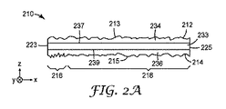
図1Aは、入力エッジ106及び出力面108を有する光ガイド104と、出力面108の隣に配置され、第1の主面112が出力面108とは反対に面し、反対側にある第2の主面114が出力面108に面する、拡散体110と、拡散体110の隣に配置され、光ガイド104とは反対側にある光学フィルム120と、光学フィルム120の隣に配置され、拡散体110の反対側にあるディスプレイパネル130と、入力エッジ106の隣に配置された光源140とを含むディスプレイ102の概略側面図である。光学フィルム120は、例えば交差したプリズムフィルムなどのBrightness Enhancement Film(BEF)でもよい。拡散体110は、本明細書で説明する拡散体のいずれかとすることができる。図1Bは、光源140と、出力面108を有する光ガイド104とを含む、ディスプレイ102の一部分の概略上面図である。例示する実施形態には、複数の光源140が含まれる。光ガイド104とディスプレイパネル130の間に好適な拡散体110が置かれていない場合、各光源140の近くの領域でホットスポットが視認されることがある。拡散体110と光ガイド104が空隙により隔てられてもよく、拡散体110と光学フィルム120が空隙により隔てられてもよい。
FIG. 1A shows an
光学フィルム120は、拡散体110の隣にある転向フィルム又は再利用フィルムを含んでもよい。好適な転向フィルム又は再利用フィルムとしては、「OPTICAL FILM」と題する、本出願と同日出願の米国仮出願第62/152486号で説明されるフィルムが挙げられ、同出願は、本説明と矛盾しない範囲で参照により本明細書に組み込まれる。そのような光学フィルムについては、本明細書の他の箇所で更に説明する。
The
図2Aは、第1の主面212と、反対側にある第2の主面214と、第1の主面212と第2の主面214との間に延在する第1のエッジ223と、反対側にある第2のエッジ225とを含む拡散体210の側面図である。第2の主面214は、第1のエッジ223の隣にある第1の部分216と、第1の部分216の隣にある第2の部分218とを含む。第1の主面212は、略一様な第1のヘーズをもたらす複数の第1の表面構造213を含む。第2の主面214は、第2の主面214の第2の部分218にわたる略一様な第2のヘーズと、第2の主面214の第1の部分216における第3のヘーズとをもたらす複数の第2の表面構造215を含む。第3のヘーズは、第1の部分216のうち第1のエッジ223に最も近い第1の領域216a(図2Bを参照)で略一定でもよく、第1の部分216の第2の領域216b(図2Bを参照)で単調に減少してもよい。
FIG. 2A shows a first
第1の構造化主面212及び第2の構造化主面214は、直交する面内方向に概ね沿って延在し、図2A〜図2Cに示すように局所的なデカルトx−y−z座標系を定義するために用いることができる。拡散体210の基準面が、x方向及びy方向に延在し、拡散体210の厚さが、z方向に沿う。x方向は、第1のエッジ223から連続境界217(図2Bを参照)に向かう方向と説明することができ、y方向は、x方向と直交する面内方向と説明することができる。y方向は、エッジ223に沿う方向と説明することもでき、x方向は、y方向と直交する面内方向と説明することができる。
The first structured
図2Aに例示する実施形態では、表面構造213は、基材層233の主面に配置された第1の層234に形成され、表面構造215は、基材層233のうち第1の層234とは反対側にある主面に配置された第2の層236に形成される。基材層233は、対向する主面237及び主面239を含む。第1の層234及び第2の層236の一方又は両方は、ツール(例えば、マイクロ複製ツール)に対して硬化性樹脂を注型して硬化させる、注型及び硬化処理により形成されてもよい。第1の層234及び/又は第2の層236の形成に用いる材料の硬化は、紫外線(UV)照射、熱、又は他の既知の任意の方法で行うことができる。代わりに、拡散体210は、単一層であり、表面構造213及び215が単一層の外側主面に直接形成されてもよい。この場合、例えば、十分な熱及び圧力で熱可塑性基材をエンボス加工することによって、第1の構造化主面及び第2の構造化主面を形成することができる。
In the embodiment illustrated in FIG. 2A, the
典型的に、拡散体を構成する1又は複数の層は、高度に光透過性であり、少なくとも可視スペクトルの大部分の光を透過させる。よって、そのような1又は複数の層は、典型的に、そのような光に対して低吸収性である。キャリアフィルム又は基材層233として用いる例示的な材料としては、ポリアクリレート及びポリメタクリレート、ポリカーボネート、ポリエチレンテレフタレート、ポリエチレンナフタレート、ポリスチレン、シクロオレフィンポリマーなどの光透過性ポリマー、コポリマー、又はそれらのポリマー分類の組合せが挙げられる。第1のパターン化層234又は第2のパターン化層236として用いる例示的な材料としては、アクリレート及びエポキシ樹脂などの光透過性ポリマーが挙げられる。しかし、他のポリマー材料及び非ポリマー材料を用いてもよい。1又は複数の層は、例えば、1.4〜1.8、又は1.5〜1.8、又は1.5〜1.7の範囲の好適な任意の屈折率を有することができるが、この範囲外の値を用いることもできる。屈折率は、550nm若しくは別の好適な設計波長で規定されてもよく、又は可視波長範囲にわたる平均値でもよい。屈折率は、25℃で規定されてもよい。
Typically, one or more layers that make up the diffuser are highly transmissive, transmitting at least most of the light in the visible spectrum. Thus, such one or more layers are typically less absorptive to such light. Exemplary materials used as carrier films or
図2Bは、拡散体210の概略下面図であり、第2の主面214の第1の部分216及び第2の部分218と、第2の主面214の第1の部分216と第2の部分218との間の連続境界217とを示している。第1の部分216は、幅W1aを有する第1の領域216aと、幅W1bを有する第2の領域216bとを含む。第1の部分216は、エッジ223の隣にあり、第2の部分218は、第1の部分216の隣にありエッジ223とは反対側にあり、第1の領域216aは、第1のエッジ223の隣にあり、第2の領域216bは、第1の領域216aと第2の部分218との間にある。第1の部分216及び第2の部分218は、拡散体210の長さLにわたって延在してもよく、又は拡散体の長さLの少なくとも90パーセントにわたって延在してもよい。第1の領域216a及び第2の領域216bは、拡散体210の長さLにわたって延在してもよく、又は拡散体の長さの少なくとも90パーセントにわたって延在してもよい。第1の領域216aは、エッジ223に隣接してもよく、第2の領域216bは、第1の領域216aに隣接してもよく、第2の部分218は、第2の領域216bに隣接してもよい。第1の部分216は、幅W1=W1a+W1bを有し、第2の部分218は、幅W2を有する。第1の部分216の第1の領域216aでは第2のヘーズよりも高く、第1の部分の第2の領域216bでは第1のエッジ223からの距離によって単調に減少し(すなわち、xによって単調に減少し)、第2の主面214の第1の部分216と第2の部分218との間の連続境界217に沿って第2のヘーズに略等しい第3のヘーズを有することによって、ヘーズの変化と関連する光学アーチファクトを生じずに、光ガイドの入力エッジの隣にある光源と関連するホットスポットを実質的に抑制できることが判明している。一部の実施形態では、第2の部分の幅W2は、拡散体の幅W1+W2の少なくとも90パーセントである。一部の実施形態では、W1をW2で割った値が、0.9よりも小さく又は0.95よりも小さい。一部の実施形態では、W1は、1mmよりも大きく、又は2mmよりも大きく、又は3mmよりも大きく、又は5mmよりも大きく、又は1cmよりも大きい。一部の実施形態では、W1a及びW1bの一方又は両方は、0.5mmよりも大きく、又は1mmよりも大きく、又は2mmよりも大きく、又は3mmよりも大きく、又は5mmよりも大きく、又は1cmよりも大きい。
FIG. 2B is a schematic bottom view of the
第1の主面212及び第2の主面214のヘーズについては、表面構造213及び215の振幅(例えば、高さ)、間隔、側方寸法(例えば、直径)及び/又は傾斜の基本分布の観点から説明することができる。それらの分布を、分布が変化する長さスケールよりも小さいが、表面構造213及び215のサイズよりも大きい領域で決定することができる。例えば、分布を、第1の部分216のエリア231及び第2の部分218のエリア232で決定してもよい。エリア231は、第1の領域216a内、第2の領域216b内でもよく、又は第1の領域216aと第2の領域216bとに跨ってもよい。エリア231又はエリア232は、本明細書の他の箇所で更に説明する平均等価円直径(ECDavg)の1、2、3、4、又は5倍の直径を有する、エリア231内の構造の円形領域でもよい。代わりに、エリア231又は232は、例えば、100マイクロメートル、又は1mm、又は2mm、又は3mm、又は5mmの固定された直径を有する円形領域でもよい。エリア231又はエリア232などの、表面のエリアのヘーズ又は透明度を、本明細書の他の箇所で更に説明するようなヘーズメーターを用いて決定することができる。一部の実施形態では、表面構造215の振幅、間隔又は傾斜の分布のうちの少なくとも1つが、第1の部分216の第2の領域216bにおけるエリア231の位置(例えば、x位置)によって変化する。一部の実施形態では、表面構造215の振幅、間隔又は傾斜の分布のうちの少なくとも1つが、第1の部分216の第1の領域216aにおけるエリア231の位置(例えば、y位置)によって変化する。一部の実施形態では、表面構造215の振幅、間隔及び傾斜の各分布が、第2の部分218におけるエリア232の位置によって変化しない。同様に、一部の実施形態では、表面構造213の振幅、間隔及び傾斜の各分布は、第1の主面212上の位置によって変化しない。一部の実施形態では、表面構造215の振幅、間隔及び傾斜の各分布は、第1の部分216の第1の領域216aにおけるエリア231のx位置によって変化しない。一部の実施形態では、表面構造215の振幅、間隔及び傾斜の分布は、y座標によって変化しない。そのような実施形態では、y座標に延在するエリアでヘーズを決定してもよい。このことは、図2Cに例示されており、エリア231cが、例えば、1mm、2mm又は3mmの幅を有する細片でもよい。
For the haze of the first
一部の実施形態では、傾斜の分布は、本明細書の他の箇所で更に説明するような表面角度分布によって特徴付け可能である。表面角度分布は、2つの直交方向(例えば、x方向及びy方向)のそれぞれの半値半幅(HWHM)により特徴付け可能でもよい。一部の実施形態では、第2の主面214の第1の部分216(例えば、エリア231又は231c)又は第2の主面214の第2の部分218(例えば、エリア232)のうちの少なくとも1つの領域が、第1の方向(例えば、x方向)の第1の半値半幅(HWHM)を有する第1の表面角度分布と、第1の方向とは異なる第2の方向(例えば、y方向)の第2のHWHMを有する第2の表面角度分布とを有する。一部の実施形態では、第1のHWHMは、第2のHWHMとは異なる。一部の実施形態では、第2の主面214の任意の領域での第1のHWHMは、その領域の第2のHWHMとは異なる。第1のHWHM及び第2のHWHMのそれぞれは、約15度よりも小さくてもよく、又は約10度よりも小さくてもよく、又は約6度よりも小さくてもよく、例えば、約1度〜、約6度、又は約10度、又は約15度の範囲内でもよい。第1のHWHMと第2のHWHMは、例えば、少なくとも1度又は少なくとも2度だけ異なってもよい。
In some embodiments, the slope distribution can be characterized by a surface angle distribution as further described elsewhere herein. The surface angle distribution may be characterized by the full width at half maximum (HWHM) of each of the two orthogonal directions (eg, the x and y directions). In some embodiments, at least of the
一部の実施形態では、第2の部分218は、第2の主面214の表面積の少なくとも90パーセント、又は少なくとも95パーセント、又は少なくとも99パーセントの表面積を有する。一部の実施形態では、第2の部分218は、第2のエッジ225まで延在しない。代わりに、ヘーズの第2の変化を含み第2のエッジ225の隣にある第3の部分があってもよい。第3の部分のヘーズの第2の変化は、第1の部分216のヘーズの変化と同様であってもよい。このタイプの拡散体は、両側面からエッジ照明されるバックライトに有用であることがある。同様に、拡散体は、第1のエッジ223と第2のエッジ225との間に延在する第3のエッジ及び第4のエッジを有してもよく、第3のエッジ及び/又は第4のエッジのそれぞれ隣にあり、ヘーズが変化しうる第4の部分及び/又は第5の部分があってもよい。
In some embodiments, the
図11は、光散乱粒子1166を含み、山1172及び谷1174を含む構造化面1171を有する、構造化層1140の断面図である。光線1175の方向は、光線1175が構造化面1171を通って出るときに屈折により変化する。構造化面1171の幾何形状が逐一変化するので、構造化面1171を通って出る光の方向のシフトは、逐一変化する。この方向のシフトの変化によって、層1140のヘーズへの表面寄与が生じる。粒子1166も、層1140のヘーズに寄与する。例えば、光線1178は、粒子1166のうちの1つ以上により散乱し、それによりヘーズに寄与する。山1172の下には谷1174の下よりも多くの粒子1166があるので、山1172を通過する光は、谷1174を通過する光よりも散乱する傾向がある。したがって、構造化層の表面構造は、構造化面との空気界面での屈折によりヘーズへの寄与を生じさせることと、構造内に含まれた粒子により散乱を生じさせることの両方によって、ヘーズをもたらすことができる。
FIG. 11 is a cross-sectional view of a
拡散体のうち構造化面を有する層によりもたらされるヘーズ又は透明度は、低ヘーズ基材(例えば、1パーセントよりも低い、又は0.5パーセントよりも低いヘーズ)上に層を再現し、本明細書の他の箇所で説明するようなヘーズメーターを用いて再現層及び基材によるヘーズ又は透明度を測定することによって、決定することができる。例えば、光学的に透明な基材上に再現された第1の層234又は第2の層236を有するサンプルを加工することができ、サンプルによるヘーズ又は透明度を測定することができる。代わりに、拡散体のうち構造化面を有する層によりもたらされるヘーズ又は透明度は、(例えば、共焦点走査型レーザー顕微鏡(CSLM)又は原子間力顕微鏡(AFM)を用いて)表面の微細構成を測定し、層の屈折率及び層に含まれうる任意の光散乱粒子の屈折率を測定し、従来の光線追跡技術を用いてヘーズ又は透明度への表面構造の寄与を計算することによって、決定することができる。
The haze or clarity provided by the layer with the structured surface of the diffuser reproduces the layer on a low haze substrate (eg, haze below 1 percent or below 0.5 percent) and is described herein. It can be determined by measuring the haze or transparency of the reproduction layer and substrate using a haze meter as described elsewhere in the book. For example, a sample having a
一部の実施形態では、拡散体は、光散乱粒子又はビーズを含まなくてもよく、又は実質的に含まなくてもよい。そのような実施形態では、所与の表面によりもたらされるヘーズは、反対側の表面の材料の屈折率にマッチングする屈折率の材料で反対側の表面をコーティングすることによって、測定することができる。ヘーズメーターの光源に面する所与の表面を有するサンプルにより測定される全体ヘーズは、所与の表面によりもたらされるヘーズとなる。所与の表面の透明度も、この屈折率マッチング技術を用いて決定することができる。 In some embodiments, the diffuser may or may not contain light-scattering particles or beads. In such an embodiment, the haze provided by a given surface can be measured by coating the opposite surface with a material of refractive index that matches the refractive index of the material of the opposite surface. The overall haze measured by a sample having a given surface facing the light source of the haze meter is the haze provided by the given surface. The transparency of a given surface can also be determined using this index of refraction matching technique.
ヘーズすなわち光学ヘーズは、ASTM D1003−13 「Standard Test Method for Haze and Luminous Transmittance of Transparent Plastics」で説明されるように測定することができる。ASTM D1003−13規格に取り挙げられており、BYK−Gardner Inc.(メリーランド州Silver Springs)から入手可能なHAZE−GARD PLUSメーターを用いてヘーズを決定することができる。ヘーズに関連する透明度すなわち光学透明度も、HAZE−GARD PLUSヘーズメーターを用いてASTM D1003−13規格に従って測定することができる。 The haze, or optical haze, can be measured as described in ASTM D1003-13 "Standard Test Method for Haze and Luminous Transparency of Transparent Plastics". It is mentioned in the ASTM D1003-13 standard and is described by BYK-Gardner Inc. Haze can be determined using the HAZE-GARD PLUS meter available from (Silver Springs, Maryland). Haze-related transparency, or optical transparency, can also be measured using a HAZE-GARD PLUS haze meter according to ASTM D1003-13 standards.
ASTM D1003−13規格で規定されるように、HAZE−GARD PLUSヘーズメーターは、サンプルにより散乱した、光源からの光を測定するために用いる、コリメート光源と積分球の間にある開口を含む。構造化層のエリアのヘーズ又は透明度は、測定されるエリアの形状の切欠きを有し、切欠きエリアの中心を開口の中心と位置合わせして開口の上に置かれたカバーシートを有するHAZE−GARD PLUSヘーズメーターを用いて、測定することができる。カバーシートは、エリアの外側の領域からの光が積分球に入るのを阻止するので、サンプルのうち切欠きエリアに及ぶエリアのみのヘーズ又は透明度が決定される。例えば、2mmスリット以外の箇所の光を阻止するカバーシートを開口の上に置くことができ、ヘーズメーターを用いて、開口の隣に置いたサンプルのヘーズを決定することができる。得られたヘーズ読取り値は、サンプルのうち2mmスリットの正面のエリアのヘーズである。例えば、サンプルのうちy方向で一様なヘーズを測定するには、2mmスリットが有用である。他の切欠き形状を用いてもよい。例えば、2mmの直径を有する円形切欠きを用いてもよく、又はエリア231、232又は231cについて本明細書の他の箇所で説明する幾何形状のうちのいずれかに対応するエリアを有する切欠きを用いてもよい。構造化面を有する層のヘーズは、コリメート光源に面する構造化面によって決定されてもよい。拡散体が、略一様なヘーズをもたらす第1の表面と、第2の表面全体にわたる非一様なヘーズをもたらす第2の表面とを有するとき、拡散体の全体ヘーズは、光源に面する第1の構造化面によって、又は光源に面し、より高いヘーズをもたらす表面によって決定されてもよい。
As specified in ASTM D1003-13 standard, the HAZE-GARD PLUS haze meter includes an aperture between the collimating light source and the integrating sphere used to measure the light from the light source scattered by the sample. The haze or transparency of the area of the structured layer has a notch in the shape of the area to be measured, HAZE with a cover sheet placed over the opening with the center of the notch area aligned with the center of the opening. -Measurement can be performed using a GARD PLUS haze meter. Since the cover sheet blocks light from the outer region of the area from entering the integrating sphere, the haze or transparency of only the area of the sample that extends to the notched area is determined. For example, a cover sheet that blocks light at locations other than the 2 mm slit can be placed on the aperture, and a haze meter can be used to determine the haze of the sample placed next to the aperture. The haze reading obtained is the haze in the area in front of the 2 mm slit in the sample. For example, a 2 mm slit is useful for measuring a uniform haze in the y direction of a sample. Other notch shapes may be used. For example, a circular notch having a diameter of 2 mm may be used, or a notch having an area corresponding to any of the geometries described elsewhere herein for
ディスプレイに用いるとき、第2の主面214が光ガイドの出力主面に面し、第1のエッジ223が光ガイドの入力エッジの隣となるように、拡散体210を光ガイドに近接して配置してもよい。第1の主面212と関連する略一様なヘーズである第1のヘーズは、第2の主面214の第2の部分218と関連する略一様なヘーズである第2のヘーズよりも高くてもよい。第1のヘーズは、少なくとも約2パーセント、少なくとも約5パーセント、少なくとも約10パーセント、又は少なくとも約15パーセント、又は少なくとも約20パーセントだけ第2のヘーズよりも高くてもよい。例えば、第1のヘーズが50パーセントであり、第2のヘーズが10パーセントである場合、第1のヘーズは、第2のヘーズよりも40パーセントだけ高い。一部の実施形態では、第2の主面214の第1の部分216と関連する第3のヘーズの最高値は、第1のヘーズよりも高い。例えば、第3のヘーズは、少なくとも約2パーセント、少なくとも約5パーセント、少なくとも約10パーセント、又は少なくとも約15パーセント、又は少なくとも約20パーセントだけ第1のヘーズよりも高くてもよい。
When used in a display, the
図3は、本説明の拡散体のヘーズ分布を例示している。拡散体の第1の主面は、略一様であり値H1を有する第1のヘーズ351をもたらす。拡散体の第2の主面は、第2の部分318(第2の部分218に対応する)の第2のヘーズ352と、第1の部分316(第1の部分216に対応する)の第3のヘーズ353とをもたらす。第1の部分316の第1の領域316a(第1の領域216aに対応する)における第3のヘーズ353は、第2の部分318における第2のヘーズ352よりも高く、第1の主面によりもたらされる第1のヘーズ351よりも高い。第2の領域316bにおける第3のヘーズ353は、第1のエッジから第1の部分316と第2の部分318との間の境界に向かう方向に沿う距離によって単調に減少する(すなわち、x座標によって単調に減少する)。拡散体は、第1の構造化主面と第2の構造化主面(例えば、第1の主面212と第2の主面214)の組合せによりもたらされる全体ヘーズ354を有する。全体ヘーズ354は、第3のヘーズ353による寄与により位置によって変化することができる。一部の実施形態では、基材(例えば、基材233)に含まれた光散乱粒子は、全体ヘーズへの追加の寄与をもたらす。全体ヘーズが第1の表面及び第2の表面による寄与の単純な線形和にならないことに留意されたい。第2の部分318における第2の主面の第2のヘーズ352は、約H2であり、第1の部分316における第2の主面の第3のヘーズ353は、最高値Hmを有する。例示する実施形態では、
Hm>H1>H2となる。
FIG. 3 illustrates the haze distribution of the diffuser of this description. The first major surface of the diffuser, resulting in a
H m > H 1 > H 2 .
ヘーズ値のこの構成は、高輝度出力をもたらす一方で、ヘーズの変化による望まれない光学アーチファクトを追加せずにホットスポットの視認性を抑制するのに特に有利であることが判明している。一部の実施形態では、Hm−H1は、少なくとも約2パーセント、又は少なくとも約5パーセント、又は少なくとも約10パーセントであり、及び/又はH1−H2は、少なくとも約2パーセント、又は少なくとも約5パーセント、又は少なくとも約10パーセントである。一部の実施形態では、Hmは、少なくとも50パーセント、又は少なくとも60パーセント、又は少なくとも70パーセントである。一部の実施形態では、H1は、約10パーセント〜、又は約15パーセント〜、約50パーセントまで、又は約60パーセントまで、又は約70パーセントまで、又は約80パーセントまで、又は約90パーセントまで、又は約95パーセントまで、又は約100パーセントまでの範囲内である。一部の実施形態では、H1は、約50パーセントよりも高く、又は約60パーセントよりも高く、又は約70パーセントよりも高い。一部の実施形態では、第1の主面は、約1パーセント〜、又は約2パーセント〜、又は約3パーセント〜、約30パーセントまで、又は約40パーセントまでの範囲内の光学透明度を有する。一部の実施形態では、H2は、約0.5パーセント〜、又は約1パーセント〜、又は約2パーセント〜、約15パーセントまで、又は約18パーセントまで、又は約20パーセントまで、又は約40パーセントまで、又は約50パーセントまで、又は約70パーセントまで、又は約90パーセントまで、又は約95パーセントまでの範囲内である。一部の実施形態では、第2の主面は、第2の主面の全ての部分及び領域で約85%以下の光学透明度を有する。一部の実施形態では、第2の主面の第1の部分又は第2の部分は、1パーセントよりも高く、又は2パーセントよりも高く、又は3パーセントよりも高く、かつ、50パーセントよりも低く、又は60パーセントよりも低く、又は90パーセントよりも低く、又は100パーセントよりも低くてもよい、光学透明度を有してもよい。一部の実施形態では、第2の主面の第2の部分は、約5パーセント〜約100パーセントの範囲内の光学透明度を有してもよく、第1の主面は、約3パーセント〜約20パーセントの範囲内の光学透明度を有してもよい。 This configuration of haze values has been found to be particularly advantageous in suppressing hotspot visibility without adding unwanted optical artifacts due to changes in haze, while providing high brightness output. In some embodiments, H m- H 1 is at least about 2 percent, or at least about 5 percent, or at least about 10 percent, and / or H 1- H 2 is at least about 2 percent, or at least. About 5 percent, or at least about 10 percent. In some embodiments, Hm is at least 50 percent, or at least 60 percent, or at least 70 percent. In some embodiments, H 1 is about 10 percent, or from about 15 percent to up to about 50 percent, or up to about 60 percent, or up to about 70 percent, or up to about 80 percent, or to about 90 percent , Or up to about 95 percent, or up to about 100 percent. In some embodiments, H 1 is greater than about 50 percent, or greater than about 60 percent, or greater than about 70 percent. In some embodiments, the first principal surface has optical transparency in the range of about 1 percent to, or about 2 percent, or about 3 percent to, about 30 percent, or up to about 40 percent. In some embodiments, H 2 is from about 0.5 percent, or about 1 percent, or about 2 percent, up to about 15 percent, or up to about 18 percent, or up to about 20 percent, or about 40. It is in the range of up to a percentage, or up to about 50%, or up to about 70%, or up to about 90%, or up to about 95%. In some embodiments, the second main surface has an optical transparency of about 85% or less in all parts and regions of the second main surface. In some embodiments, the first or second portion of the second main surface is higher than 1 percent, higher than 2 percent, higher than 3 percent, and greater than 50 percent. It may have optical transparency, which may be lower, lower than 60 percent, lower than 90 percent, or lower than 100 percent. In some embodiments, the second portion of the second main surface may have optical transparency in the range of about 5 percent to about 100 percent, and the first main surface may have from about 3 percent to about 3 percent. It may have an optical transparency in the range of about 20 percent.
代替的なヘーズ分布を図3Bに示している。第1の主面は、略一定の第1のヘーズ351bをもたらし、第2の主面の第2の部分は、略一定の第2のヘーズ352bをもたらし、第2の主面の第1の部分は、第1の部分の第1の領域で略一定の値353aを取り、第2の主面の第2の部分の第2の領域で単調に減少する値353bを有する第3のヘーズをもたらす。
An alternative haze distribution is shown in Figure 3B. The first main surface provides a substantially constant
本明細書で説明するいずれの実施形態でも、第2の主面の第1の部分の第2の領域における第3のヘーズは、図3Bに例示するように線形的に単調に減少してもよく、又は単調に減少するヘーズは、x座標の多項式関数又は区分定義された多項式関数により説明されうる。多項式関数は、三次スプラインでありうるスプラインでもよい。三次スプラインなどの非線形関数によって、単純な線形減少関数よりも光学アーチファクトが抑制されることが判明している。 In any of the embodiments described herein, the third haze in the second region of the first portion of the second main surface may decrease linearly and monotonically as illustrated in FIG. 3B. A well or monotonically decreasing haze can be explained by an x-coordinate polynomial function or a compartmentally defined polynomial function. The polynomial function may be a spline that can be a cubic spline. Non-linear functions such as cubic splines have been found to suppress optical artifacts more than simple linear decrement functions.
第1の部分216のヘーズは、y座標に依存してもよく、依存しなくてもよい。図3C及び図3Dは、第1の部分216の固定されたx座標についてy座標に応じた第3のヘーズ353c及び353dをそれぞれ示している。x座標は、第1の領域216a又は第2の領域216bのいずれにあってもよい。第3のヘーズ353cは、y座標に依存しないが、第3のヘーズ353dは、y座標によって周期的に変化する。第3のヘーズは、例えば、一様性を向上させるために、エッジ照明型ディスプレイに含まれたLEDに対応して周期的に変調されてもよい。ヘーズの最高領域は、ホットスポットが生じうる領域であってもよい。ホットスポット領域は、バックライトに用いる抽出器の構成を理由に、LEDの場所からオフセットすることがある。一部の場合、抽出器がLED間の場所にホットスポットを発生させることがあるので、ヘーズの最高領域をLED間に置くことが望ましいことがある。
The haze of the
一部の実施形態では、拡散体の全体ヘーズは、ヘーズの急な変化によりもたらされる光学アーチファクトが生じないように、拡散体全体で滑らかに変化する。しかし、第2の主面214の第1の部分216における第2の領域216bの幅W1bの長さスケールで、ヘーズが著しく変化することが望ましいことがある。この長さスケールは小さい(例えば、拡散体の全体幅(W1+W2)の10パーセントよりも小さい)が、拡散体の第1の主面が、第2の主面のヘーズの変化により生じうる任意のアーチファクトを隠せる一様なヘーズを有する場合、ヘーズは、望ましくない光学アーチファクトを実質的に伴わずに幅W1bのスケールで変化することができる。ヘーズの急激な変化による光学アーチファクトを回避すると同時に、幅W1bの長さスケールでヘーズを著しく変化させるために、光の波長よりも大きい、又は画素サイズよりも大きい、又は本明細書の他の箇所で更に説明する平均等価円直径(ECDavg)よりも大きい長さスケールでヘーズが徐々に変化することが望ましいことがある。一部の実施形態では、このことは、十分に大きいW1bを選ぶことによって達成される。例えば、W1bは、約0.5mmよりも大きく、又は約1mmよりも大きく、又は約2mmよりも大きく、又は約3mmよりも大きく、又は約5mmよりも大きくてもよい。
In some embodiments, the overall haze of the diffuser changes smoothly throughout the diffuser so that the optical artifacts caused by abrupt changes in the haze do not occur. However, it may be desirable for the haze to change significantly on the length scale of the width W 1b of the
ヘーズは、ヘーズの急な遷移がない場合、連続的に又は略連続的に変化すると考えられうる。例えば、第1の部分216の第3のヘーズは、第3のヘーズが第2の主面上の位置によって急に変化しない場合、略連続的に変化すると考えられうる。第1の位置と第2の位置が互いに0.1mm以内にあるときに、第1の位置の第1のヘーズ値が、第2の位置の第2のヘーズ値とは10パーセントを超えて異なる場合、ヘーズが急に変化すると考えられうる。一部の実施形態では、第3のヘーズは、第1の部分216で急な変化を示さない。一部の実施形態では、0.1mm以下だけ離れた、又は0.5mm以下だけ離れた、第1の位置と第2の位置との各対について、第1の位置の第3のヘーズと第2の位置の第3のヘーズとの間の大きさの差が、20パーセントよりも小さく、又は10パーセントよりも小さい。
The haze can be considered to change continuously or substantially continuously in the absence of abrupt transitions in the haze. For example, the third haze of the
望ましいヘーズ分布を生じさせる任意のタイプの構造化面を用いてもよい。例としては、プリズムがランダムに変形しうる、又は不均等に離間しうるプリズム構造又はプリズム状構造と、不均等に離間し、一方向にある程度伸びうるランダム又は不規則な構造と、直交する2つの面内方向に沿うサイズが限定されうる他のランダム又は不規則な構造とが挙げられる。 Any type of structured surface that produces the desired haze distribution may be used. As an example, it is orthogonal to a prism structure or prismatic structure in which the prisms can be deformed randomly or evenly separated, and a random or irregular structure in which the prisms are unevenly separated and can extend to some extent in one direction. Other random or irregular structures may be limited in size along one in-plane direction.
第2の構造化主面は、例えば、基材233の側面239に層236を印刷することによって、加工されてもよい。勾配を有するパターンを印刷して、ヘーズの望ましい勾配を生じさせることができる。印刷は、例えば、オフセット印刷又はインクジェット印刷を用いて行ってもよい。透明樹脂又はビーズ充填樹脂を印刷して、層236を形成してもよい。例えば、ガラスビーズ又はポリマービーズを有するか又は有しないUV硬化性アクリル樹脂を用いてもよい。印刷パターンは、高さ、間隔及び/又は直径若しくは側方寸法の勾配を有する、小ドット又は小型レンズの形をとってもよい。代わりに、高さ、間隔、側方寸法、及び/又は傾斜分布の勾配を伴うパターンを有する複製ツールに対する注型及び硬化によって、第2の構造化主面を加工することができる。
The second structured main surface may be processed, for example, by printing
第1の主面212が、国際公開第2014/081693号(Pham等)で概ね説明されるように形成された表面構造を有すること、及び/又は第2の主面214が、米国特許第8,657,472号(Aronson等)又は同第8,888,333号(Yapel等)で概ね説明されるように形成された表面構造を有することが特に有利であることが判明しているが、一部の場合、第2の主面のヘーズが、米国特許第8,657,472号(Aronson等)又は同第8,888,333号(Yapel等)の表面のヘーズよりも高くなることが望ましいことがある。国際公開第2014/081693号(Pham等)、米国特許第8,657,472号(Aronson等)、及び米国特許第8,888,333号(Yapel等)のそれぞれは、本説明と矛盾しない範囲で参照により本明細書に組み込まれる。国際公開第2014/081693号(Pham等)に従って形成された構造は、役立つ程度のヘーズ及び光学透明度をもたらす一方、米国特許第8,657,472号(Aronson等)又は同第8,888,333号(Yapel等)に従って形成された構造は、有用な程度のヘーズ及び光学透明度をもたらしながら、ディスプレイの光ガイドに隣接して置かれたときに光学的な欠陥を防止する密着防止機能ももたらす。本明細書の他の箇所で更に議論するように、米国特許第8,657,472号(Aronson等)又は同第8,888,333号(Yapel等)の構造を作製するのに用いるツールを、第2の主面214の第1の部分216におけるヘーズが連続的に変化するように適合させることができる。第1の主面及び第2の主面の一方の説明に用いる、ECDの大きさ又は傾斜度の分布などの数量は、他の主面を説明する際にも用いることができる。
The first
国際公開第2014/081693号(Pham等)で説明されるような第1の主面と、米国特許第8,657,472号(Aronson等)又は米国特許第8,888,333号(Yapel等)で説明されるような第2の主面とを形成するときには、第1の主面が、第2の主面の第2の部分のヘーズ(第2のヘーズ)よりも高いヘーズ(第1のヘーズ)を有することが望ましいことがある。これは、少なくとも2つの理由による。第1に、第2のヘーズが増加する場合、望ましい全体ヘーズを生じさせるために第1のヘーズを低下させることが望ましいことがあり、国際公開第2014/081693号(Pham等)のメッキ処理を用いて、より低いヘーズの表面を作製するには多くの時間及びコストを要することになる。第2に、第1の主面がディスプレイの出力方向に面するように、ディスプレイに置かれるように拡散体を構成することができる。そのような構成では、高いヘーズを有する第1の構造化主面は、再利用効果をもたらすことによって、ディスプレイの正面輝度を高めることに寄与することができる。更に、第2の主面の第1の部分におけるヘーズの変化により生じうる任意のアーチファクトを隠すために、相対的に高い第1のヘーズを役立てることができる。 The first aspect, as described in WO 2014/081693 (Pham et al.), And U.S. Pat. No. 8,657,472 (Aronson et al.) Or U.S. Pat. No. 8,888,333 (Yapel et al.) ), The first main surface is higher than the haze (second haze) of the second part of the second main surface (first). It may be desirable to have a haze). This is for at least two reasons. First, if the second haze increases, it may be desirable to lower the first haze in order to produce the desired overall haze, and the plating process of International Publication No. 2014/081693 (Pham et al.) It will take a lot of time and cost to make a lower haze surface in use. Second, the diffuser can be configured to be placed on the display so that the first main surface faces the output direction of the display. In such a configuration, the first structured main surface with a high haze can contribute to increasing the front luminance of the display by providing a reusable effect. In addition, a relatively high first haze can be used to hide any artifacts that may result from changes in the haze in the first portion of the second main surface.
第1の構造化主面212又は第2の構造化主面214の微細構成は、第1の構造化主面212又は第2の構造化主面214と平行な基準面(x−y平面)に対する厚さ方向(z軸)に沿う偏差の観点から表すことができる。多くの場合、構造化面の微細構成は、独立した別個の構造を特定できるようなものである。そのような構造は、構造化面ツールの対応する窪みにより作られた出っ張りの形をとってもよく、又は構造化面ツールの対応する出っ張りにより作られた窪みの形をとってもよい。構造は、典型的に、直交する2つの面内方向に沿うサイズが制限される。例えば、第1の構造化主面212又は第2の構造化主面214を平面図で見るとき、独立した構造は、典型的に、任意の面内方向に沿って線形態様で無限に延在することがない。出っ張り又は窪みのいずれにしても、構造は、一部の場合、稠密に詰まっていてもよく、すなわち、隣り合う多くの構造又は大部分の構造の境界の少なくとも部分が実質的に交わるか、又は合致するように配置されてもよい。構造は、構造化面に不規則に又は非一様に分散してもよい。一部の場合、構造のうちの一部、大部分、又は略全て(例えば、>90%、又は>95%、又は>99%)は、湾曲していてもよく、又は丸みを帯びた、そうでなければ湾曲した基面を備えてもよい。一部の場合、構造のうちの少なくとも一部が、ピラミッド形状でもよく、そうでなければ略平坦な切子面により定義されてもよい。所与の構造のサイズは、平面図における等価円直径(ECD)の観点から表すことができ、構造化面の構造は、例えば、15マイクロメートルよりも小さい、又は10マイクロメートルよりも小さい、又は4〜10マイクロメートル、又は4〜15マイクロメートルの範囲内の平均ECDを有してもよい。構造化面及び構造は、本明細書の他の箇所で議論するような他のパラメータ、例えば、ECDなどの特徴的な横寸法に対する深さ又は高さのアスぺクト比、又は平面図上の単位エリア当たり表面におけるリッジの全長によって、特徴付けることもできる。構造化面に、又は構造化面上に、又は拡散体内のどこかにビーズを使用せずに、拡散体の光学ヘーズ、光学透明度、及び他の特徴をもたらすことができる。
The microstructure of the first structured
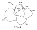
独立した個別の構造を特定できる構造化面の場合、構造の横寸法又は面内寸法などの特徴的なサイズの観点から構造化面を説明することができる。各構造は、例えば、最大横寸法、最小横寸法、及び平均横寸法を有するとして特徴付けられてもよい。独立した構造が、直交する2つの面内方向に沿うサイズで制限される場合、例えば、いずれの面内方向に沿っても線形態様で無限に延在することがない場合、各構造は、等価円直径「ECD」を有するとして特徴付けられてもよい。所与の構造のECDは、平面図における構造のエリアと同じであるエリアを平面図において有する円の直径として定義することができる。例えば、図4を参照すると、仮想的な構造化面420aの平面図を示している。構造化面は、出っ張り又は窪みでありうる識別可能な構造421a、421b、421c、421dを備える。構造421aには円423aが重ね合わされており、円は、この平面図において構造421aのエリアと凡そ等しいエリアを有する。円423aの直径(ECD)は、構造421aの等価円直径(ECD)である。構造化面の代表的な領域における全ての構造のECD値を平均することによって、それらの構造化面又は構造は、平均等価円直径ECDavgを有すると考えられうる。
In the case of a structured surface that can specify an independent individual structure, the structured surface can be described in terms of a characteristic size such as a lateral dimension or an in-plane dimension of the structure. Each structure may be characterized as having, for example, a maximum lateral dimension, a minimum lateral dimension, and an average lateral dimension. Each structure is equivalent if the independent structures are limited in size along two orthogonal in-plane directions, for example, if they do not extend indefinitely in a linear fashion along either in-plane direction. It may be characterized as having a circular diameter "ECD". An ECD of a given structure can be defined as the diameter of a circle having an area in the plan that is the same as the area of the structure in the plan. For example, referring to FIG. 4, a plan view of a virtual structured
例示的な構造の高さについて、図5における仮想的な構造化面の図面に例示している。図では、光学拡散フィルム520が、構造化主面520aを有するパターン化層522を含む。構造化面520aは、認識できる独立した構造521a、521bを含む。構造化面は、x−y平面に沿って延在し、又はx−y平面を定義する。x−y平面と平行な3つの基準面、RP1、RP2、及びRP3を示している。基準面RP1、RP3は、(それぞれ)構造521aの最高部分及び最低部分の観点から定義されてもよい。基準面RP2は、ゼロ又は略ゼロの曲率に対応する位置に配置されてもよく、つまり、その位置の表面は、ピークの上部に置けるように内側に湾曲しておらず、窪みの下部に置けるように外側に湾曲してもいない。それらの基準面を仮定して、RP1とRP2の間の高さh1と、RP2とRP3の間の高さh2を定義することができる。構造の平均高さを|h1|と|h2|の平均として定義することができる。一部の実施形態では、第1の構造化面は、基準面(例えば、基準面RP2)における等価円直径(ECD)と、厚さ方向に沿う平均高さとによって特徴付けられる稠密に詰まった構造を含み、各構造のアスぺクト比が、構造の平均高さを構造のECDで割った値に等しい。一部の実施形態では、構造の平均アスぺクト比が、0.15よりも小さく、又は0.10よりも小さい。一部の実施形態では、構造の平均アスぺクト比が、0.01〜0.15の範囲内である。
The height of the exemplary structure is illustrated in the drawing of the virtual structured surface in FIG. In the figure, the
一部の実施形態では、稠密に詰まった構造は、リッジ状の特徴を生じる傾向にあるが、リッジ状の特徴は、稠密に詰まった構造がない場合に生じることもある。図6における仮想的な構造化面の図面には、リッジを例示している。図では、光学拡散フィルムが構造化主面620aを含む。構造化面620aは、認識できる独立した構造621a、621b、621cを含む。構造化面は、x−y平面に沿って延在し、又はx−y平面を定義する。長く鋭ったピーク領域として説明されうるリッジが、構造621a、621bの境界が集まる少なくとも短いセグメントに沿って形成される。リッジ又はセグメントは、点p1、p2、p3を含む。既知の微細構成に基づく、それらの各点での局所的な傾斜及び曲率は、勾配と平行でありリッジと垂直である方向(軸a1、a2、a3を参照)に沿って、及び勾配と垂直でありリッジと平行である方向(軸b1、b2、b3を参照)に沿って計算することができる。そのような曲率及び傾斜を用いて、点が長く鋭ったピーク領域にあることを確認することができる。例えば、2つの垂直方向(例えばa1、b1)に沿う十分に異なる曲率、リッジと垂直である(例えばa1)鋭った曲率、勾配方向(例えばリッジに沿う、b1を参照)にあり平均傾斜よりも小さい傾斜、及び十分に長いセグメント長によって、リッジ上の点を特定してもよい。
In some embodiments, densely packed structures tend to produce ridge-like features, which may occur in the absence of densely packed structures. The ridge is illustrated in the drawing of the virtual structured surface in FIG. In the figure, the optical diffusion film includes a structured
第1の構造化主面及び/又は第2の構造化主面は、平面図の単位エリア当たりにおける、200mm/mm2よりも短い、若しくは150mm/mm2よりも短い、又は10〜200mm/mm2、若しくは10〜150mm/mm2の範囲内の全リッジ長によって特徴付けられてもよい。
The first structured main surface and / or the second structured main surface is shorter than 200 mm / mm 2 or shorter than 150 mm / mm 2 or 10 to 200 mm / mm per unit area in the plan view. It may be characterized by a total ridge length in the range of 2 or 10-150 mm /
サンプルのエリア当りリッジ長は、国際公開第2014/081693号(Pham等)で説明されるように決定することができる。この技術では、所与の拡散体サンプルについて、サンプルの中心部分から約1x1cmのサンプル片が切り出される。サンプル片は、顕微鏡スライドに装着され、特徴付けられるその構造化面は、Au−Pdスパッタコーティングされる。共焦点走査型レーザー顕微鏡(CSLM)を用いて、構造化面の2つの高さプロファイルが得られる。可能であればいつでも、微細構成の良好なサンプリングを与えるように視野が選ばれる。本明細書の他の箇所で説明する原理に従って高さプロファイルを分析するために、リッジ分析が用いられる。 The ridge length per area of the sample can be determined as described in WO 2014/081693 (Pham et al.). In this technique, for a given diffuser sample, a sample piece of about 1x1 cm is cut out from the central portion of the sample. The sample piece is mounted on a microscope slide and its structured surface characterized by Au-Pd sputter coating. A confocal scanning laser scanning microscope (CSLM) is used to obtain two height profiles of the structured surface. Whenever possible, the field of view is chosen to give good sampling of the microstructure. Ridge analysis is used to analyze the height profile according to the principles described elsewhere herein.
リッジ分析は、2D高さマップ上でリッジのピークを特定し、単位サンプルエリア当たりのリッジの全長を計算することを可能にする。各画素について、勾配方向に沿う曲率及び勾配方向と交差する曲率を計算することができる。曲率及び傾斜の閾値処理を行ってリッジを特定することができる。 Ridge analysis identifies the peak of the ridge on a 2D height map and makes it possible to calculate the total length of the ridge per unit sample area. For each pixel, the curvature along the gradient direction and the curvature intersecting the gradient direction can be calculated. Ridges can be identified by performing curvature and slope thresholding.
以下は、リッジ分析に用いうるリッジの定義である。
1.曲率の定義:(a)g曲率は、勾配方向に沿う曲率である。(b)t曲率は、勾配方向と交差する(垂直な)方向に沿う曲率である。(c)g曲率は、勾配に沿う3つの点を用いて3つの点に外接する円を計算することによって計算される。g曲率=1/R、ここで、Rは、この円の半径である。(d)t曲率は、勾配と交差する方向に沿う3つの点を用いて3つの点に外接する円を計算することによって計算される。g曲率=1/R、ここで、Rは、この円の半径である。(e)曲率は、それらの3つの点の中心点に割り当てられる。(f)3つの点の間隔は、着目していない微細な特徴による寄与を抑制するほど十分に大きいが、着目した特徴による寄与を保つほど十分に小さくなるように選ばれる。
2.リッジ上の点の曲率は、2つの垂直方向の間で十分に異なる。(a)g曲率とt曲率は、少なくとも2倍だけ異なる(いずれかがより大きくなりうる)。
3.リッジは、谷の大部分よりも鋭っている。(a)曲率は、g曲率分布の1パーセンタイル点の絶対値よりも大きい(g曲率の1%が、1パーセンタイル点よりも小さい)。
4.傾斜は、平均傾斜よりも小さい。(a)リッジ上のg傾斜(勾配に沿う傾斜)が、表面の平均g傾斜よりも小さい。(b)リッジの上部の傾斜は、非常に傾斜した表面上にない限り、典型的に略ゼロである。
5.リッジは、十分に長い。(a)潜在的なリッジは、その全長(分岐を含む)が、潜在的なリッジ上部に沿う平均曲率半径よりも小さい場合には、リッジとみなされない。(b)潜在的なリッジは、その全長が潜在的なリッジの平均幅の3分の1よりも小さい場合には、リッジとみなされない。(c)これらの寸法が概略測定されることに留意されたい。
6.分岐は、十分に長い。(a)リッジの中央セクションからの分岐は、リッジの平均幅の1.5倍よりも大きい場合には、リッジの連続部とみなされる。そうでなければ、分岐は除去される。(b)これらの寸法が概略測定されることに留意されたい。
The following is a definition of ridge that can be used for ridge analysis.
1. 1. Definition of Curvature: (a) g Curvature is the curvature along the gradient direction. (B) The t-curvature is the curvature along the (vertical) direction intersecting the gradient direction. (C) The g-curvature is calculated by calculating a circle circumscribing the three points using the three points along the gradient. g Curvature = 1 / R, where R is the radius of this circle. (D) The t-curvature is calculated by calculating a circle circumscribing the three points using the three points along the direction intersecting the gradient. g Curvature = 1 / R, where R is the radius of this circle. (E) Curvature is assigned to the center points of those three points. (F) The distance between the three points is selected so as to be sufficiently large to suppress the contribution of the unfocused fine feature, but sufficiently small to maintain the contribution of the focused feature.
2. The curvature of the points on the ridge is sufficiently different between the two vertical directions. (A) The g-curvature and the t-curvature differ by at least two times (either can be greater).
3. 3. The ridge is sharper than most of the valley. (A) The curvature is larger than the absolute value of the 1st percentile point of the g-curvature distribution (1% of the g-curvature is smaller than the 1st percentile point).
4. The slope is smaller than the average slope. (A) The g-slope on the ridge (slope along the slope) is smaller than the average g-slope on the surface. (B) The slope of the top of the ridge is typically approximately zero unless it is on a very sloped surface.
5. The ridge is long enough. (A) A potential ridge is not considered a ridge if its overall length (including branches) is less than the average radius of curvature along the potential ridge top. (B) A potential ridge is not considered a ridge if its overall length is less than one-third of the average width of the potential ridge. (C) Note that these dimensions are roughly measured.
6. The branch is long enough. (A) A branch from the central section of a ridge is considered a continuum of the ridge if it is greater than 1.5 times the average width of the ridge. Otherwise, the branch is removed. (B) Note that these dimensions are roughly measured.
リッジを特定した後、高さマップにおける全てのリッジの全長が計算され、高さマップのエリアで割られる。 After identifying the ridges, the total length of all ridges on the height map is calculated and divided by the area of the height map.
一部の実施形態では、フーリエパワースペクトルを用いて、拡散体の第1の主面又は第2の主面の空間的な不規則性又はランダム性の程度が決定される。微細構成は、構造化面が延在する基準面に対して定義することができる。例えば、拡散体210の第1の構造化主面212(図2Aを参照)は、概ねx−y平面にあり、概ねx−y平面に沿って延在する。x−y平面を基準面として用いて、基準面内の位置に応じた、基準面に対する第1の主面212の高さとして、すなわち、(x,y)位置に応じた表面のz座標として、第1の構造化主面212の微細構成を説明することができる。表面のz座標は、表面プロファイル又は高さプロファイルH(x,y)と称されることがある。このような方法で構造化面の微細構成を測定する場合、微細構成関数の空間周波数成分を分析して、表面の空間的な不規則性又はランダム性の程度を決定する(又は構造化面に存在する空間的な周期性を特定する)ことができる。
In some embodiments, the Fourier power spectrum is used to determine the degree of spatial irregularity or randomness of the first or second main surface of the diffuser. The microstructure can be defined for a reference plane on which the structured plane extends. For example, the first structured
一般的な手法は、高速フーリエ変換(FFT)関数を用いて空間周波数成分を分析することである。微細構成が、直交する2つの面内方向(x及びy)に沿う高さ情報を提供するため、表面の空間周波数成分は、各面内方向に沿う空間周波数成分を分析することによって十分に特徴付けられる。構造化面における十分に大きい代表的な部分にわたる微細構成を測定し、各面内方向のフーリエパワースペクトルを計算することによって、空間周波数成分を決定することができる。得られた2つのパワースペクトルを、パワースペクトル密度(PSD)−空間周波数のグラフにプロットすることができる。得られた曲線が局所的な任意の周波数ピーク(ゼロ周波数に対応しない)を含む範囲で、そのようなピークの大きさを、図7と関連して他の箇所で更に説明する「ピーク率」の観点から表すことができる。 A common technique is to analyze the spatial frequency components using the Fast Fourier Transform (FFT) function. The spatial frequency components of the surface are well characterized by analyzing the spatial frequency components along each in-plane direction, as the microstructure provides height information along two orthogonal in-plane directions (x and y). Can be attached. Spatial frequency components can be determined by measuring the microstructure over a sufficiently large representative portion of the structured surface and calculating the Fourier power spectrum in each in-plane direction. The two power spectra obtained can be plotted on a power spectrum density (PSD) -spatial frequency graph. To the extent that the resulting curve contains any local frequency peaks (not corresponding to zero frequencies), the magnitude of such peaks is described further elsewhere in connection with FIG. 7 "Peak Rate". It can be expressed from the viewpoint of.
フーリエパワースペクトルを決定する詳細な手順については、国際公開第2014/081693号(Pham等)で説明されている。この手法では、所与の拡散体サンプルについて、サンプルの中心部分から約1x1cmのサンプル片が切り出される。サンプル片は、顕微鏡スライドに装着され、特徴付けられるその構造化面は、Au−Pdスパッタコーティングされる。共焦点走査型レーザー顕微鏡(CSLM)を用いて、構造化面の2つの高さプロファイルが得られる。可能であればいつでも、微細構成の良好なサンプリング及び存在する任意の周期性を与えるように視野が選ばれる。2次元(2D)パワースペクトル密度(PSD)は、各2D高さプロファイルについて計算される。2D PSDは、2D高さプロファイルH(x,y)の2D空間フーリエ変換の大きさの自乗である。MATALBの高速フーリエ変換(FFT)関数を用いてPSDを計算するために、MATLABが用いられる。2D高さプロファイルの有限な空間寸法により生じるFFT中のリンギングを抑制するのに役立てるために、FFTを用いる前に、2D高さプロファイルに2Dハミング窓が適用される。2D PSDは、x方向で合計されて、(ダウンウェブ方向でありうる)y方向の1次元(1D)PSDを与える。同様に、2D PSDは、y方向で合計されて、(クロスウェブ方向でありうる)x方向の1D PSDを与える。 The detailed procedure for determining the Fourier power spectrum is described in WO 2014/081693 (Pham et al.). In this method, for a given diffuser sample, a sample piece of about 1x1 cm is cut out from the central portion of the sample. The sample piece is mounted on a microscope slide and its structured surface characterized by Au-Pd sputter coating. A confocal scanning laser scanning microscope (CSLM) is used to obtain two height profiles of the structured surface. Whenever possible, the field of view is chosen to give good sampling of the microstructure and any periodicity present. Two-dimensional (2D) power spectral density (PSD) is calculated for each 2D height profile. 2D PSD is the square of the magnitude of the 2D spatial Fourier transform of the 2D height profile H (x, y). MATLAB is used to calculate the PSD using the MATLAB Fast Fourier Transform (FFT) function. A 2D humming window is applied to the 2D height profile before using the FFT to help suppress ringing in the FFT caused by the finite spatial dimensions of the 2D height profile. The 2D PSDs are summed in the x direction to give a one-dimensional (1D) PSD in the y direction (which can be the downweb direction). Similarly, the 2D PSDs are summed in the y direction to give a 1D PSD in the x direction (which can be cross-web direction).
空間周波数ピークに関する1D PSDの分析について、図7と関連して説明する。この図には、仮想的なフーリエパワースペクトル曲線を例示目的で示している。上で議論した1D PSD関数(x又はy)のいずれかを表しうる曲線が、パワースペクトル密度(PSD)−空間周波数のグラフ上に現れる。垂直軸(PSD)は、ゼロで始まる線形スケール上にプロットされることが想定される。曲線は、(a)ゼロ周波数に対応せず、(b)基準線を定義する隣り合う2つの谷内に留まる、周波数ピークを有するとして示されている。隣り合う2つの谷は、空間周波数f1で点p1により特定され、空間周波数f2で点p2により特定される。周波数f1は、ピークが始まる周波数とみなすことができ、周波数f2は、ピークが終わる周波数とみなすことができる。基準線は、p1とp2を結ぶ直線セグメント(破線)である。ピークの大きさは、グラフ上のエリアA及びBの観点から表すことができる。エリアAは、周波数ピークと基準線の間にあるエリアである。エリアBは、基準線の下又は真下のエリアである。つまり、B=(PSD(f1)+PSD(f2))*(f2−f1)/2である。A+Bの合計は、周波数ピークの下又は真下のエリアである。これらの定義を仮定すると、以下のような相対ピーク振幅、すなわち「ピーク率」の観点からピークの大きさを定義することができる。
ピーク率=A/(A+B)。
The analysis of 1D PSD with respect to spatial frequency peaks will be described in connection with FIG. In this figure, a virtual Fourier power spectrum curve is shown for illustration purposes. A curve that can represent any of the 1D PSD functions (x or y) discussed above appears on the power spectral density (PSD) -spatial frequency graph. The vertical axis (PSD) is expected to be plotted on a linear scale starting at zero. The curve is shown as having a frequency peak that (a) does not correspond to zero frequency and (b) stays in two adjacent valleys that define the reference line. Two adjacent valleys are identified by the point p1 at the spatial frequency f1 and by the point p2 at the spatial frequency f2. The frequency f1 can be regarded as the frequency at which the peak starts, and the frequency f2 can be regarded as the frequency at which the peak ends. The reference line is a straight line segment (broken line) connecting p1 and p2. The magnitude of the peak can be expressed from the viewpoint of areas A and B on the graph. Area A is an area between the frequency peak and the reference line. Area B is an area below or directly below the reference line. That is, B = (PSD (f1) + PSD (f2)) * (f2-f1) / 2. The sum of A + B is the area below or directly below the frequency peak. Assuming these definitions, the peak magnitude can be defined from the viewpoint of the following relative peak amplitude, that is, "peak rate".
Peak rate = A / (A + B).
各サンプルについて2つの1D PSD(x方向で1つ、y方向で1つの、2つのフーリエパワースペクトル)を評価することができ、フーリエパワースペクトルが任意の周波数ピークを含む範囲で、各曲線の最も卓越したピークを特定することができる。各曲線の最も卓越したピークについて、上で説明したピーク率を計算することができる。最も卓越したピークが測定されるので、計算されたピーク率は、所与のフーリエパワースペクトル中に存在しうる全てのピークの上限である。このようにしてピーク率を決定する例については、国際公開第2014/081693号(Pham等)で説明されている。 Two 1D PSDs (one in the x direction, one in the y direction, two Fourier power spectra) can be evaluated for each sample, and the most of each curve, as long as the Fourier power spectrum contains any frequency peak. You can identify outstanding peaks. For the most prominent peaks on each curve, the peak rates described above can be calculated. The calculated peak rate is the upper limit of all peaks that may be present in a given Fourier power spectrum, as the most predominant peaks are measured. An example of determining the peak rate in this way is described in International Publication No. 2014/081693 (Pham et al.).
一部の実施形態では、第1の主面は、直交する第1の面内方向及び第2の面内方向とそれぞれ関連する第1のフーリエパワースペクトル及び第2のフーリエパワースペクトルにより特徴付け可能である微細構成を有し、第1のフーリエパワースペクトルが、ゼロ周波数に対応せず、第1の基準線を定義する隣り合う2つの谷内に留まる、1つ以上の第1の周波数ピークを含む限り、そのような任意の第1の周波数ピークが、0.8よりも小さい、又は0.7よりも小さい第1のピーク率を有し、第2のフーリエパワースペクトルが、ゼロ周波数に対応せず、第2の基準線を定義する隣り合う2つの谷内に留まる、1つ以上の第2の周波数ピークを含む限り、そのような任意の第2の周波数ピークが、0.8よりも小さい、又は0.7よりも小さい第2のピーク率を有する。 In some embodiments, the first principal plane can be characterized by a first Fourier power spectrum and a second Fourier power spectrum that are associated with the orthogonal first in-plane and second in-plane directions, respectively. The first Fourier power spectrum does not correspond to zero frequency and contains one or more first frequency peaks that remain in two adjacent valleys that define the first reference line. As long as any such first frequency peak has a first peak rate less than 0.8 or less than 0.7 and the second Fourier power spectrum corresponds to the zero frequency. Any such second frequency peak is less than 0.8, as long as it contains one or more second frequency peaks that remain within two adjacent valleys that define the second reference line. Or it has a second peak rate less than 0.7.
本説明の拡散体の第1の主面又は第2の主面のいずれかを特徴付ける別の数量は、表面の傾斜分布である。傾斜分布は、比較的緩やかな傾斜(例えば、大部分の傾斜が40度よりも小さい)を有することが望ましい実施形態における第2の主面の特に有用な特徴付けをもたらす。一部の実施形態では、第2の主面の第2の部分の約20パーセント以下、又は約10パーセント以下、又は約7パーセント以下、又は約5パーセント以下、又は約3パーセント以下が、約20度よりも大きい、又は約15度よりも大きい、又は約10度よりも大きい、又は約7度よりも大きい、又は約5度よりも大きい、又は約3.5度よりも大きい傾斜度を有する。一部の実施形態では、第2の表面主面は、より急な傾斜を有してもよい。例えば、一部の実施形態では、第2の主面の約20パーセント以下、約10パーセント以下、約7パーセント以下が、約20度よりも大きい、又は約30度よりも大きい、又は約35度よりも大きい、又は約40度よりも大きい傾斜度を有する。一部の実施形態では、第2の主面の相当な部分が、1度よりも大きい傾斜度を有し、第2の主面の相当な部分が、10度よりも小さい、又は15度よりも小さい傾斜度を有する。一部の実施形態では、第2の主面の第2の部分の少なくとも約50パーセント、又は少なくとも約70パーセント、又は少なくとも約80パーセント、又は少なくとも約85パーセント、又は少なくとも約90パーセントが、1度よりも大きい傾斜度を有する。一部の実施形態では、第2の主面の第2の部分の約85パーセント以下、又は約80パーセント以下が、約15度よりも大きい、又は約10度よりも大きい傾斜度を有する。 Another quantity that characterizes either the first or second main surface of the diffuser of the present description is the slope distribution of the surface. The slope distribution provides a particularly useful characterization of the second main surface in embodiments where it is desirable to have a relatively gentle slope (eg, most slopes are less than 40 degrees). In some embodiments, about 20 percent or less, or about 10 percent or less, or about 7 percent or less, or about 5 percent or less, or about 3 percent or less of the second portion of the second main surface is about 20. Greater than a degree, or greater than about 15 degrees, or greater than about 10 degrees, or greater than about 7 degrees, or greater than about 5 degrees, or having an inclination greater than about 3.5 degrees .. In some embodiments, the second surface main surface may have a steeper slope. For example, in some embodiments, about 20 percent or less, about 10 percent or less, about 7 percent or less of the second main surface is greater than about 20 degrees, greater than about 30 degrees, or about 35 degrees. Has a degree of inclination greater than or greater than about 40 degrees. In some embodiments, a significant portion of the second main surface has a degree of inclination greater than 1 degree and a significant portion of the second main surface is less than 10 degrees or greater than 15 degrees. Also has a small slope. In some embodiments, at least about 50 percent, or at least about 70 percent, or at least about 80 percent, or at least about 85 percent, or at least about 90 percent of the second portion of the second main surface is once. Has a greater inclination than. In some embodiments, about 85 percent or less, or about 80 percent or less, of the second portion of the second main surface has an inclination greater than about 15 degrees or greater than about 10 degrees.
図8は、構造化層840の一部分の概略側面図である。構造化層840は、例えば、図2Aの第2の層236に対応することができる。図8は、主面842とは反対側にある主面814の、マイクロ構造でありうる構造860を示している。構造860は、構造の表面にわたる傾斜分布を有する。例えば、構造は、場所810の傾斜θを有し、ここで、θは、場所810の構造面と垂直な(α=90°)垂線820と、同じ場所の構造860の表面と接する接線830との間の角度である。傾斜θは、接線830と層840の主面842との間の角度でもある。
FIG. 8 is a schematic side view of a part of the structured
例えば、原子間力顕微鏡(AFM)又は共焦点走査型レーザー顕微鏡(CSLM)を用いて、表面プロファイルH(x,y)(すなわち、直交する面内座標x及びyに応じた基準面の上方の表面の高さH)を決定することによって、第1の主面又は第2の主面を特徴付けることができる。以下の2つの式によって、x方向及びy方向のそれぞれに沿う傾斜Sx及びSyを計算することができる。

以下の式によって、傾斜度Smを計算することができる。
x方向の傾斜分布及びy方向の傾斜分布並びに傾斜度を決定することができる。 The inclination distribution in the x direction, the inclination distribution in the y direction, and the degree of inclination can be determined.
一部の実施形態では、第2の主面の第1の部分又は第2の主面の第2の部分における少なくとも1つの領域が、第1の方向の第1の半値半幅(HWHM)を有する第1の表面角度分布(例えば、x方向の傾斜の分布Sxが、σxのHWHMを有しうる)と、第1の方向とは異なる第2の方向の第2の半値半幅(HWHM)を有する第2の表面角度分布(例えば、y方向の傾斜の分布Syが、σyのHWHMを有しうる)とを有する。一部の実施形態では、第1のHWHMは、第2のHWHMに略等しく、一部の実施形態では、第1のHWHMは、第2のHWHMとは異なる。例えば、|σx−σy|が、約1度〜、約5度まで、又は約10度まで、又は約15度までの範囲内である。一部の実施形態では、σx及びσyのそれぞれが、約1度〜、約10度まで、又は約15度までの範囲内である。一部の実施形態では、σx及びσyの大きい方と、σx及びσyの小さい方との比率は、1よりも大きく、又は1.1よりも大きく、又は1.2よりも大きく、又は1.5よりも大きく、かつ、15よりも小さく、又は10よりも小さく、又は5よりも小さい。一部の実施形態では、|σx−σy|をσx+σyで割った値は、0.05よりも大きく、又は0.1よりも大きく、又は0.2よりも大きい。 In some embodiments, at least one region in the first portion of the second main surface or the second portion of the second main surface has a first full width at half maximum (HWHM) in the first direction. The first surface angle distribution (for example, the distribution S x of the inclination in the x direction may have HWHM of σ x ) and the second half width at half maximum (HWHM) in the second direction different from the first direction. It has a second surface angle distribution having (for example, the distribution S y of the inclination in the y direction may have an HWHM of σ y). In some embodiments, the first HWHM is substantially equal to the second HWHM, and in some embodiments, the first HWHM is different from the second HWHM. For example, | σ x −σ y | is in the range of about 1 degree to about 5 degrees, or up to about 10 degrees, or up to about 15 degrees. In some embodiments, each of σ x and σ y is in the range of about 1 degree to about 10 degrees, or up to about 15 degrees. In some embodiments, the larger the sigma x and sigma y, the ratio of the smaller of sigma x and sigma y is greater than 1, or greater than 1.1, or greater than 1.2 , Or greater than 1.5 and less than 15, or less than 10, or less than 5. In some embodiments, the value of | σ x − σ y | divided by σ x + σ y is greater than 0.05, greater than 0.1, or greater than 0.2.
構造の分布は、構造の振幅(例えば、山から谷への高さ)を変化させること、又は隣り合う構造間の間隔を変化させることによって、変化させることができる。一部の実施形態では、第2の主面は、振幅分布及び間隔分布を有する表面構造を含み、振幅分布及び間隔分布の少なくとも一方が、第2の主面の第1の部分を通して変化し、振幅分布及び間隔分布のそれぞれが、第2の主面の第2の部分において略一様である。高さ分布、及び/又は間隔分布、及び/又は構造の形状分布を変化させることによって、傾斜分布を変化させることができる。一部の実施形態では、第2の主面は、第2の主面の第1の部分を通して略連続的に変化し(例えば、第1のエッジ223から第2の主面214の第1の部分216と第2の部分218の間の連続境界217まで略連続的に変化する傾斜分布)、第2の主面の第2の部分において略一様な傾斜分布を有する表面構造を含む。
The distribution of structures can be changed by changing the amplitude of the structure (eg, the height from peak to valley) or by changing the spacing between adjacent structures. In some embodiments, the second main surface comprises a surface structure having an amplitude distribution and an interval distribution, at least one of the amplitude distribution and the interval distribution changing through the first portion of the second main surface. Each of the amplitude distribution and the interval distribution is substantially uniform in the second part of the second main surface. The slope distribution can be changed by changing the height distribution and / or the spacing distribution and / or the shape distribution of the structure. In some embodiments, the second main surface changes substantially continuously through the first portion of the second main surface (eg, the first of the
一部の実施形態では、第1の主面は、構造化面を有するツールによるマイクロ複製により作製される。ツールの構造化面は、国際公開第2014/081693号(Pham等)で説明されるように、第1の電気メッキ処理により金属を電気溶着することによって金属の第1の層を形成し、第1の平均粗度を有する第1の層の主面を生じさせること、第2の電気メッキ処理により第1の層に金属を電気溶着することによって第1の層の主面に金属の第2の層を形成し、第1の平均粗度よりも小さい第2の平均粗度を有する第2の層の主面を生じさせることによって、作製することができ、第2の層の主面がツールの構造化面に対応する。 In some embodiments, the first main surface is made by micro duplication with a tool having a structured surface. The structured surface of the tool forms a first layer of metal by electroplating the metal by a first electroplating process, as described in WO 2014/081693 (Pham et al.). By producing a main surface of the first layer having an average roughness of 1, and by electroplating the metal to the first layer by the second electroplating treatment, a second layer of metal is formed on the main surface of the first layer. It can be made by forming a layer of the second layer and producing a main surface of the second layer having a second average roughness smaller than the first average roughness. Corresponds to the structuring aspect of the tool.
図9は、例えば、拡散体の第1の主面などの構造化面を作製するプロセスの例示的なバージョン901を示している。プロセスのステップ902では、金属層が電気メッキされうる下地の役割を果たしうる基部又は基材が用意される。基材は、例えばシート、プレート、又はシリンダなど、多くの形のうちの1つを取ることができる。円形シリンダは、連続ロール商品の生成に用いることができる点で有利である。基材は、典型的に金属製であり、例示的な金属としては、ニッケル、銅、及び真ちゅうが挙げられる。しかし、他の金属を用いてもよい。基材は、後続のステップで電気溶着層が形成される露出面(「基面」)を有する。基面は、平滑かつ平坦でもよく、又は略平坦でもよい。研磨された平滑なシリンダの外側湾曲面は、特に、シリンダの表面上の所与の点の付近にある局所的な小領域を考慮するときには、略平坦であるとみなすことができる。基面は、基部平均粗度により特徴付けられてもよい。この点に関して、基面の表面「粗度」、又は本明細書で述べる他の表面「粗度」は、平均粗度Ra又は自乗平均粗度Rrmsなどの一般的に認められた任意の粗度測定値により数量化されてもよく、粗度は、問題となる表面の該当エリア全体を正しく表すのに十分大きなエリアにわたり測定されることが想定される。
FIG. 9 shows an
プロセス901のステップ903では、第1の電気メッキ処理により基材の基面に金属の第1の層が形成される。このステップが始まる前に、基材の基面を下塗りしてもよく、そうでなければ接着性を高めるように処理してもよい。金属は、基面を構成するものと実質的に同じ金属でもよい。例えば、基面が銅を含む場合、ステップ903で形成される第1の電気メッキ層も銅で作られてもよい。金属の第1の層を形成するために、第1の電気メッキ処理は、第1の電気メッキ溶液を用いる。第1の電気メッキ溶液の組成、例えば、溶液に用いる金属塩のタイプ、及び、電流密度、メッキ時間、及び基材速度などの他のプロセスパラメータは、第1の電気メッキ層が平滑かつ平坦に形成されず、代わりに、構造化され、不規則な平坦切子面特徴により特徴付けられた第1の主面を有するように、選択される。不規則な特徴のサイズ及び密度は、電流密度、メッキ時間、及び基材速度により決定される一方、第1の電気メッキ溶液に用いる金属塩のタイプは、特徴の幾何形状を決定する。この点に関する更なる教示は、米国特許出願公開第2010/0302479号(Aronson等)に見出すことができる。第1のメッキ処理は、第1の電気メッキ層の第1の主面が、基材の基部平均粗度よりも大きい第1の平均粗度を有するように行われる。
In
ステップ903で、第1の平均粗度のその構造化主面を有する金属の第1の電気メッキ層が作製された後、第2の電気メッキ処理によってステップ904で金属の第2の電気メッキ層が形成される。金属の第2の層は、第1の電気メッキ層を覆い、それらの組成が略同じでありうるので、2つの電気メッキ層は、もはや識別可能ではなくなることがあり、第1の層の第1の主面は、略跡形もなくなり、もはや検出可能ではなくなることがある。それにもかかわらず、第2の電気メッキ処理は、第2の電気メッキ層の露出した第2の主面が、構造化され非平坦ではあるが、第1の主面の第1の平均粗度よりも小さい第2の平均粗度を有するような方法である点で、第1の電気メッキ処理とは異なる。第2の電気メッキ処理は、第1の主面よりも抑制された粗度を第2の主面に提供するために、多くの点で第1の電気メッキ処理とは異なってもよい。
After the first electroplating layer of the metal having its structured main surface of the first average roughness is made in
一部の場合、ステップ904の第2の電気メッキ処理は、ボックス904aに示すように、少なくとも有機レベラーを添加することによって、第1の電気メッキ溶液とは異なる第2の電気メッキ溶液をステップ903で用いてもよい。有機レベラーは、小さい穴には比較的厚い堆積を生じさせ、小さい出っ張りには比較的薄い堆積を生じさせ、小さい表面不規則性の深さ又は高さを最終的に小さくする可能性をメッキ槽に取り入れる材料である。レベラーによって、メッキ部位は、素地金属よりも大きい表面平滑度を有する。例示的な有機レベラーとしては、非限定的に、スルホン化硫化ヒドロカルビル化合物、アリルスルホン酸、様々な種類のポリエチレングリコール、及び、バイチオカルバメート又はチオ尿素及びそれらの誘導体を含むチオカルバメートが挙げられうる。第1の電気メッキ溶液は、多くても微量の有機レベラーを含んでもよい。第1の電気メッキ溶液は、100、又は75、又は50ppmよりも低い全体濃度の有機炭素を有してもよい。第1の電気メッキ溶液中の任意の有機レベラーの濃度に対する第2の電気メッキ溶液中の有機レベラーの濃度の比率は、例えば、少なくとも50、又は100、又は200、又は500でもよい。第2の主面の平均粗度は、第2の電気メッキ溶液中の有機レベラーの量を調節することによって、調整することができる。
In some cases, the second electroplating process of
ステップ904の第2の電気メッキ処理も、又は代わりに、第1の主面よりも第2の主面の粗度を抑制する効果を有する少なくとも1つの電気メッキ技術又は特徴を第2のステップ904に含めることによって、ステップ903の第1の電気メッキ処理とは異なってもよい。シービング(thieving)(ボックス904b)及びシールディング(shielding)(ボックス904c)は、そのような電気メッキ技術又は特徴の例である。更に、有機レベラーに加えて又はその代わりに、1つ以上の有機微細化剤(ボックス904d)を第2の電気メッキ溶液に添加して、第2の主面の平均粗度を抑制してもよい。
The second electroplating process of
ステップ904が完了した後、第1の電気メッキ層及び第2の電気メッキ層を有する基材は、光学拡散フィルムを形成するオリジナルツールとして用いることができる。一部の場合、ツールの構造化面、すなわち、ステップ904で生成された、第2の電気メッキ層の第2の構造化主面を不動態化してもよく、そうでなければ、第2の金属又は他の好適な材料で保護してもよい。例えば、第1の電気メッキ層及び第2の電気メッキ層を銅で構成する場合、第2の構造化主面をクロムの薄いコーティングで電気メッキすることができる。クロム又は他の好適な材料の薄いコーティングは、第2の構造化主面の微細構成及び平均粗度を実質的に保つほど十分に薄いことが好ましい。
After
光学拡散フィルムの製作に際してオリジナルツール自体を用いるのではなく、オリジナルツールの第2の構造化主面をマイクロ複製することによって、1つ以上の複製ツールを作製してもよく、複製ツール(1つまたは複数)を用いて、拡散体の構造化面を製作してもよい。オリジナルツールから作製された第1の複製は、第2の構造化主面に対応するが、その反転された形態である第1の複製構造化面を有する。例えば、第2の構造化主面の出っ張りは、第1の複製構造化面の窪みに対応する。第1の複製から第2の複製が作製されてもよい。第2の複製は、オリジナルツールの第2の構造化主面に対応し、その反転されていない形態である、第2の複製構造化面を有する。 One or more duplication tools may be produced by micro-duplicate the second structured main surface of the original tool, rather than using the original tool itself in the production of the optical diffusing film. Alternatively, a plurality of) may be used to produce a structured surface of the diffuser. The first replica made from the original tool corresponds to the second structured main surface, but has a first duplicate structured surface which is an inverted form thereof. For example, the bulge of the second structured main surface corresponds to the depression of the first duplicate structured surface. A second copy may be made from the first copy. The second replica corresponds to the second structured main surface of the original tool and has a second duplicate structured surface, which is an uninverted form thereof.
ステップ904の後、構造化面ツールを作製した後に、オリジナルツール又は複製ツールからのマイクロ複製によって、(オリジナルツールに対して反転されているか反転されていないかにかかわらず)同じ構造化面を有する光学拡散フィルムをステップ906で作製することができる。第1の構造化主面は、例えば、事前形成フィルムのエンボス加工、又はキャリアフィルム上での硬化層の注型及び硬化を含む、好適な任意の処理によりツールから形成されてもよい。
After
図10は、例えば、ヘーズが変化する第2の主面の構造化面などの構造化面を生成するためにマイクロ複製できるツールの切削に用いることができる切削ツールシステム1000の概略側面図である。切削ツールシステム1000は、ねじ切り旋盤旋削処理により、駆動体1030によって中心軸1020の周囲を回転する、及び/又はこれに沿って移動することができるロール1010と、ロール材料を切削するためのカッター1040とを含む。カッターは、サーボ1050に装着され、駆動体1060によってx方向に沿ってロールの中、及び/又はロール沿いに移動させることができる。一般的に、カッター1040は、ロール及び中心軸1020に対して垂直に装着され、ロールが中心軸の周りを回転する際にロール1010の刻装可能な材料に送り込まれる。次に、カッターは、中心軸と平行に駆動されて、ねじ切りを生成する。カッター1040は、高頻度かつ低変位で同時に作動して、例えば、マイクロ複製時に構造860をもたらす特徴をロール内に生成することができる。
FIG. 10 is a schematic side view of a
サーボ1050は、高速ツールサーボ(FTS)であり、固体圧電(PZT)装置(PZTスタックと称されることが多い)を含むが、このPZTスタックは、カッター1040の位置を迅速に調節する。FTS1050によって、カッター1040のx方向、y方向、及び/若しくはz方向、又は軸外方向での高精密な高速動作が可能になる。カッター1040は、x方向、y方向及び/又はz方向に移動できるので、x方向及びy方向のいずれか又は両方で変化する振幅又は傾斜の分布を有する構造化面を形成することができる。サーボ1050は、静止位置に関して制御された動作を生じうる、任意の高品質変位サーボであってもよい。一部の場合、サーボ1050は、約0.1マイクロメートルよりも高い分解能で0〜約20マイクロメートルの範囲内の変位を確実にかつ繰り返しもたらすことができる。
駆動体1060は、カッター1040をx方向に沿って中心軸1020と平行に移動させることができる。一部の場合、駆動体1060の変位分解能は、約0.1マイクロメートルよりも高く、又は約0.01マイクロメートルよりも高い。駆動体1030により生じる回転運動は、駆動体1060により生じる並進運動と同期して、結果として得られる構造860の形状を正確に制御する。
The
切削ツールシステム1000を用いて、第1の構造化主面212(図2Aを参照)の形成に用いうるツールを作製することができ、及び/又は切削ツールシステム1000を用いて、第2の構造化主面214の形成に用いうるツールを作製することができる。第2の構造化主面214を形成するツールの作製に用いるとき、駆動体1030により生じる回転運動及び駆動体1060により生じる並進運動は、ツールのうち第2の構造化主面214の第1の部分216に対応する部分における振幅分布、間隔分布、構造形状分布、及び傾斜分布のうちの1つ以上の変化を生じさせるように選択される。
The
ロール1010の刻装可能な材料は、カッター1040により刻装できる任意の材料でもよい。例示的なロール材料としては、銅などの金属、様々なポリマー、及び様々なガラス材料が挙げられる。カッター1040は任意のタイプのカッターでもよく、用途に望ましい任意の形状を有することができる。好適なカッターについては、米国特許第8,657,472号(Aronson等)又は同第8,888,333号(Yapel等)で説明されている。
The engravable material of the
第2の構造化主面は、例えば、事前形成フィルムのエンボス加工、又は基材上での硬化層の注型及び硬化を含む、好適な任意の処理により得られたツールから形成されてもよい。オリジナルツール又はツールの複製を用いて、本明細書の他の箇所で説明するように構造化面を形成してもよい。 The second structured main surface may be formed from a tool obtained by any suitable treatment, including, for example, embossing of a preformed film or casting and curing of a cured layer on a substrate. .. The original tool or a copy of the tool may be used to form a structured surface as described elsewhere herein.
一部の実施形態では、光学フィルムと、光学フィルムの構造化下面に面する拡散体の構造化上面(例えば、第1の主面112又は212)を有し、光学フィルムと略同一の広がりを有する、本説明の光学拡散体のうちのいずれかとを含む光学スタックが提供される。光学フィルムは、第1の方向に沿って線形に延在する略平行な複数の上部構造を備える構造化上面と、第1の方向とは異なる第2の方向に沿って線形に延在する略平行な複数の下部構造を備える構造化下面とを含み、上部構造及び下部構造のそれぞれが、構造の基部の対向する第1の端部及び第2の端部からそれぞれ延在し、構造のピークで交わる、対向する第1の湾曲面及び第2の湾曲面を備えてもよい。一部の実施形態では、光学フィルムと光学拡散体は、それらの対応するエッジに沿って接合されて、光学フィルムと光学拡散体の間に空隙を形成する。一部の実施形態では、構造化上面及び構造化下面のそれぞれが、略ランダムに配置された複数の構造を備える。一部の実施形態では、光学拡散体は、光学フィルムの構造化下面に面する構造化上面であって、構造化上面にわたる略一様な第1の光学ヘーズを有する構造化上面と、構造化下面の第1のエッジに沿う第1の部分と、第1の領域から構造化下面の反対側にある第2のエッジまで延在する第2の部分とを有する構造化下面であって、第1の部分の少なくとも一部の領域が、第1の光学ヘーズ以上の第3の光学ヘーズを有し、第2の部分は、第2の部分にわたる略一様な第2の光学ヘーズを有し、第2の光学ヘーズは、第1の光学ヘーズよりも低い、構造化下面とを含む。一部の実施形態では、上面の第1の光学ヘーズは、略一様であり、約70%よりも高く、拡散体の第1の部分の第1の領域における第3の光学ヘーズは、約95%よりも高く、第2の主面の第2の部分の第2の光学ヘーズは、略一様であり、約70%よりも低い。
In some embodiments, the optical film has a structured upper surface of the diffuser facing the structured lower surface of the optical film (eg, a first
一部の実施形態では、光源と、光源に近接した入力面、及び出力面を有する光ガイドと、光ガイドに配置された、本説明の光学拡散体のうちのいずれかと、光学拡散体に配置された光学フィルムとを含むバックライトが提供される。一部の実施形態では、光学拡散体は、構造化上面であって、構造化上面にわたる略一様な第1の光学ヘーズを有する構造化上面と、光ガイドの出力面に面する構造化下面であって、構造化下面の第1のエッジに沿い光ガイドの入力面に近接する第1の部分と、第1の部分から構造化下面の反対側にある第2のエッジまで延在する第2の部分とを有し、第1の部分の少なくとも第1の領域が、第1の光学ヘーズ以上の第3の光学ヘーズを有し、第2の部分は、第2の部分にわたる略一様な第2の光学ヘーズを有し、第2の光学ヘーズは、第1の光学ヘーズとは異なる、構造化下面とを有する。光学フィルムは、光学拡散体の構造化上面に面する略線形の平行な複数の第1の構造を含む第1の構造化面と、光学拡散体の構造化上面とは反対に面する略線形の平行な複数の第2の構造を含む第2の構造化面とを含み、第1の構造及び第2の構造はそれぞれ、対向する第1の湾曲面及び第2の湾曲面を備え、第1の湾曲面と第2の湾曲面は、異なる曲率軸を有する。 In some embodiments, the light source, an optical guide having an input surface and an output surface close to the light source, one of the optical diffusers of the present description arranged on the optical guide, and an optical diffuser. Backlights including with optical film are provided. In some embodiments, the optical diffuser is a structured upper surface that has a substantially uniform first optical haze over the structured upper surface and a structured lower surface that faces the output surface of the optical guide. A first portion along the first edge of the structured lower surface and close to the input surface of the optical guide, and a second portion extending from the first portion to the second edge on the opposite side of the structured lower surface. It has two parts, at least the first region of the first part has a third optical haze above the first optical haze, and the second part is substantially uniform over the second part. The second optical haze has a structured lower surface that is different from the first optical haze. The optical film has a first structured surface containing a plurality of substantially linear parallel first structures facing the structured upper surface of the optical diffuser and a substantially linear surface opposite to the structured upper surface of the optical diffuser. The first structure and the second structure include a second structured surface including a plurality of parallel second structures, respectively, and the first structure and the second structure have a first curved surface and a second curved surface facing each other. The curved surface of 1 and the curved surface of the second have different axes of curvature.
図17は、本説明の拡散体と共に有利に用いうる例示的な光学フィルムの分割された正面側立断面図である。光学フィルム1700は、マイクロ構造1712を有する構造化上面1710と、第1の面1722及び第2の面1724を伴うマイクロ構造を有する構造化下面1720とを含む。
FIG. 17 is a split front side sectional view of an exemplary optical film that can be advantageously used with the diffusers of the present description. The
図17では、構造化面(構造化上面1710及び構造化下面1720)は、マイクロ構造の長さ方向が概ね平行にならないように配置されている。一部の実施形態では、マイクロ構造の長さ方向は、互いに直交するように配向される。しかし、構造化上面と構造化下面の両方の同時に存在する断面を一層容易に示すために、(図18と共に)図17は、分割された正面側立断面図であり、つまり、各構造化面の左にある基準座標系が示唆するように、図は、実際には繋ぎ合わされた2つの斜視図である。
In FIG. 17, the structured surfaces (structured
構造化上面1710は、マイクロ構造1712を含む。一部の実施形態では、構造化上面は、平行な複数のマイクロ構造を含む。一部の実施形態では、平行なマイクロ構造は、線形のマイクロ構造でもよい。線形は、1つのマイクロ構造のピークが、(例えば、上部平面図で見ると)構造化上面を横切る線であることを意味する。一部の実施形態では、製造プロセスの限界を含む現実的な理由から、線形のマイクロ構造は、厳密な線形からの小さな偏差を含んでもよい。一部の実施形態では、マイクロ構造は、周期的又は非周期的なピッチの変化を除いて、線形でもよい。一部の実施形態では、マイクロ構造は、線形でもよいが、周期的又は非周期的のいずれかで高さが変化してもよい。一部の実施形態では、隣り合うマイクロ構造間に空間又は「ランド」があってもよい。一部の実施形態では、構造化上面1710は、隣り合うマイクロ構造間の、約0.5μm〜約5μmの範囲内の間隔を含んでもよい。間隔は、一定でもよく又は変化してもよい。
The structured
マイクロ構造1712は、実質的に湾曲していてもよい。一部の実施形態では、マイクロ構造1712は、略シリンダ又は略半シリンダの形状を有する。一部の実施形態では、マイクロ構造1712は、マイクロ構造の長さと直交する断面に沿う半円又は半楕円である。一部の実施形態では、マイクロ構造1712は、マイクロ構造1712の基部と直交する線に沿ってマイクロ構造1712のピークからマイクロ構造1712の基部までで測定される高さhにより特徴付けられる。構造化上面1710の最低点を用いて、マイクロ構造1712の基部を決定してもよい。マイクロ構造1712は、曲率半径Rにより特徴付けられてもよく、h/Rの比率は、好適な任意の値でもよい。一部の実施形態では、h/Rは、0.4以下である。
The
一部の実施形態では、構造の面のうち構造が延在する方向にわたって取られた全断面の曲率中心をまとめて、曲率「軸」と称してもよい。一部の実施形態では、湾曲面の曲率軸は異なる。 In some embodiments, the centers of curvature of all cross-sections of the surface of the structure taken over the extending direction of the structure may be collectively referred to as the "axis" of curvature. In some embodiments, the axis of curvature of the curved surface is different.
構造化上面1710は、好適な任意の方法及び好適な任意の材料で形成されてもよい。例えば、構造化上面1710は、選択的にエッチング又は研削されてもよい。一部の実施形態では、構造化上面1710は、少なくとも部分的に2つの光子マスタリング処理によって形成されてもよい。一部の実施形態では、構造化上面1710は、反転形状のツールを利用する注型及び硬化処理に依存する。一部の場合、構造化上面は、適切な光露出が、樹脂を硬化させ、モールド又はツールから分離させ、その形状を恒久的に保持するような、UV架橋性又はUV硬化性の樹脂から形成されてもよい。一部の実施形態では、構造化上面1710は、3D印刷などの追加の工程により形成されてもよい。一部の実施形態では、構造化上面1710は、射出成形されてもよい。構造化上面1710は、モノリシックな材料片に形成されてもよく、又は基材又は寸法的に安定した層若しくは耐反り性の層に配置された材料の上部層に形成されてもよい。透明度、耐傷性若しくは耐摩耗性、耐反り性、複屈折性若しくはその欠如、マイクロ複製の可能性、ヘーズ、Tg(ガラス遷移温度)、他の表面との潜在的な接合性、又は他の好適な任意の特徴などの、材料特性、物理特性、又は光学特性のために、1つ又は複数の材料が選択されてもよい。
The structured
構造化下面1720は、第1の面1722及び第2の面1724をそれぞれに有するマイクロ構造を含む。構造化上面1710の場合と同じように、マイクロ構造は、線形のマイクロ構造でもよいが、この図に示す例示的な構成では、上部構造及び下部構造のマイクロ構造が、互いに略直交して伸びるように、図17では斜視図が分割されていることを思い出されたい。構造化下面1720は、一部の実施形態では0.5μm〜3μmの間隔で、離間した隣り合う構造を含んでもよい。
The structured
第1の面1722は、略平坦であり、マイクロ構造の長さと直交する断面により直線として現れる。他の実施形態では、第1の面1722は、ある程度の曲率を有してもよい。第2の面1724は、湾曲しており、マイクロ構造の長さと直交する断面により弧又は曲線として現れる。一部の実施形態では、マイクロ構造は、例えば、2つよりも多い面、又は2つの面とピーク又は接合部分とを含んでもよい。一部の実施形態では、第2の面1724は、一定の曲率を有してもよく、又は区分定義された曲率を有してもよい。一部の実施形態では、第2の面1724は、連続的に変化する曲率を有してもよい。一部の実施形態では、各第1の面は、同じ又は略同じ形状及びサイズでもよい。一部の実施形態では、各第2の面は、同じ又は略同じ形状及びサイズでもよい。一部の実施形態では、第1の面及び第2の面の1つ以上は、周期的に、非周期的に、又はある勾配のいずれかで、形状又はサイズの1つ以上が変化してもよい。
The
光学フィルム1700は、全体的に、好適な任意の材料又は材料の組合せから形成され、好適な任意の寸法を有してもよい。一部の実施形態では、光学フィルム1700は、特定の表示用途又は照明用途のためにサイズ決定又は形状決定されてもよい。光学フィルム1700の構造化面の構造は、説明したように直交して伸びてもよく、又は第1の方向及び第2の方向に単純に延在し又は伸びてもよく、ここで、第1の方向と第2の方向は、互いに異なる。例えば、第1の方向と第2の方向との間の角度は、78〜90度でもよい。一部の実施形態では、構造化上面及び構造化下面は、同じエリアに及んでもよい。一部の実施形態では、構造化上面1710及び構造化下面1720は、同じモノリシックフィルムの2つの側面でもよい。一部の実施形態では、2つの構造化面又はそれらのそれぞれの基材は、互いに積層されてもよく又は取り付けられてもよい。
The
図18は、光学フィルム及び拡散体を含むバックライトの分割された正面側立断面図である。バックライト1800は、マイクロ構造1812を有する構造化上面1810と、第1の面1822及び第2の面1824を含む構造化下面1820と、任意選択的な中間層1830とを有する光学フィルム1802を含む。バックライト1800は、拡散体1840、光ガイド1850、反射体1860、及び光源1870を更に含む。
光学フィルム1802は、図17に示す光学フィルムと同様に、マイクロ構造1812を有する構造化上面1810と、第1の面1822及び第2の面1824を伴うマイクロ構造を有する構造化下面1820とを含む。光学フィルム1802は、例えば、反射偏光子、又は反射偏光子と1/4波長層若しくは1/4波長プレートとの組合せでありうる中間層1830も含む。図18の中間層1830は、簡略化されており、それ自体が、1/4波長プレートと線形反射偏光子の両方を表してもよいが、それらは、別個の層として取り扱われてもよい。光学フィルム1802は、モノリシック層でもよく、又はいくつかの積層部分又は層により形成されてもよい。
FIG. 18 is a divided front side sectional view of the backlight including the optical film and the diffuser. The
The
中間層1830又は中間層1830の部品としての使用に適した反射偏光子は、多層反射偏光子でもよい。多層反射偏光子は、適切に配向されたときに、強め合う干渉により特定の偏光を反射する、適切な厚さの内部屈折率界面を有する、交互する高屈折率層と低屈折率層の共押出しされた束から形成される。反射偏光子の例としては、DBEF及びAPF(ミネソタ州St.Paulにある3M Companyから入手可能)が挙げられる。 The reflective polarizer suitable for use as a component of the intermediate layer 1830 or the intermediate layer 1830 may be a multilayer reflective polarizer. A multi-layer reflective polarizer is a combination of alternating high and low index layers with an internal index of refraction interface of appropriate thickness that reflects specific polarized light due to intensifying interference when properly oriented. Formed from extruded bundles. Examples of reflective polarizers include DBEF and APF (available from 3M Company in St. Paul, Minnesota).
バックライト1800の残りは、光学フィルム1802と光ガイド1850の間に配置された拡散体1840、光ガイド1850自体、反射体1860、及び光源1870を含む。拡散体1840は、拡散体の第1の部分(例えば、部分216)が光源1870の最も近くに配置された、本明細書で説明する拡散体のうちのいずれかとすることができる。
The rest of the
一部の実施形態では、拡散体1840は、光ガイド1850又は光学フィルム1802の略全てのエリアに及んでもよい。一部の実施形態では、拡散体1840は、光ガイド1850又は構造化下面1820のピークに対する物理的損傷を防止するように設計されてもよい。損傷には、例えば、衝撃又は衝突などのショックを受けた後の、引っ掻き傷又は構造化面の部分的な曲げ若しくは破損が含まれうる。特定の用途では、拡散体1840は、緩衝作用を適切に生じさせる特徴など、ショック吸収に有利な物理特性を有してもよい。
In some embodiments, the
一部の実施形態では、拡散体1840は、光ガイド1850及び光学フィルム1802の1つ以上に積層又は取り付けられてもよい。拡散体1840は、例えば、感圧層若しくは光学的に透明な接着層で、又は1片以上のエッジテープ若しくはリムテープによって、光ガイド1850に取り付けられてもよい。一部の実施形態では、拡散体1840は、低屈折率接着層で光ガイド1850に接合されてもよい。そのような低屈折率接着層は、複数の間隙を含んでもよい。
In some embodiments, the
光ガイド1850は、好適な任意のサイズ又は形状でもよく、好適な任意の材料から形成されてもよい。一部の実施形態では、光ガイド1850は、例えば、射出成形されたアクリル製のモノリシック片でもよく、又は他の好適な任意の材料から形成されてもよい。光ガイド1850は、高透過性、低吸収性、若しくは低散乱性などの有利な光学的特徴、又は剛性、可撓性、若しくは耐温度性及び耐反り性などの有利な物理的特徴のために選択された材料を有してもよい。一部の実施形態では、光ガイド1850は、楔状の光ガイドでもよい。一部の実施形態では、光ガイド1850は、印刷されたドット、ネガティブなマイクロ特徴(すなわち、空気/光ガイド界面が、臨界未満角度での光の散乱又は反射により内部全反射を無効にする傾向があり、光ガイドの他の表面に光を通過させる凹み)、又はポジティブなマイクロ特徴などの抽出特徴を含んでもよく、又は収容してもよい。抽出特徴は、光ガイドのエリア(終局的に、バックライト1800全体)にわたって光が均質に抽出されるような勾配パターンで配置されてもよい。言い換えると、抽出特徴は、光ガイドのうち全体的により多くの光がある、光源に近接するエリアなどの部分に、稠密に詰まっていなくてもよい。代わりに、一部の用途では、抽出特徴は、電話キーパッドその他の数字又はボタンの下などの、多くの光出力が望まれるエリアに稠密に詰まっていてもよい。抽出特徴は、サイズ、形状、及び数が、周期的に、ある勾配で、又は非周期的に、変化してもよい。
The
反射体1860は、広帯域光反射体である好適な任意の層である。一部の実施形態では、反射体1860は、アルミニウム若しくは銀などの金属反射体、又は金属反射面が置かれた基材である。一部の実施形態では、反射体1860は多層光学フィルムである。
本明細書で説明する多層光学フィルム反射偏光子と同様に、多層光学フィルム反射体は、注意深く選択され、配向されると複屈折を創り出しうる、ポリマー材料の交互する高屈折率層と低屈折率層を含む。層は、共押出しされ、強め合う干渉により広域の光スペクトルが層間の界面で反射するように配向される。各層対の光学厚さは、異なる層対が、異なる波長の光の反射に寄与するように設計される。例示的な多層光学フィルム反射体は、Enhanced Specular ReflectorすなわちESR(ミネソタ州St.Paulにある3M Companyから入手可能)である。好適な反射体は、光のうち少なくとも90%、95%、98%、又は99%さえ反射することができる。反射体は、拡散面(又は均等拡散面)、鏡面、又は半鏡面として特徴付けられる反射パターンを提供することができる。
Reflector 1860 is any suitable layer that is a broadband light reflector. In some embodiments, the reflector 1860 is a metal reflector such as aluminum or silver, or a substrate on which a metal reflective surface is placed. In some embodiments, the reflector 1860 is a multilayer optical film.
Similar to the multilayer optical film reflectors described herein, multilayer optical film reflectors are carefully selected and oriented to create birefringence, alternating high index layers and low index of polymer material. Includes layers. The layers are co-extruded and oriented so that a broad optical spectrum is reflected at the interface between the layers due to intensifying interference. The optical depth of each layer pair is designed so that different layer pairs contribute to the reflection of light of different wavelengths. An exemplary multilayer optical film reflector is an Enhanced Specular Reflector or ESR (available from 3M Company in St. Paul, Minnesota). Suitable reflectors can reflect at least 90%, 95%, 98%, or even 99% of the light. The reflector can provide a reflective pattern characterized as a diffusing surface (or even diffusing surface), a mirror surface, or a semi-mirror surface.
光源1870は、好適な任意の光源又は光源の組合せでもよい。発光ダイオード(LED)、冷陰極蛍光管(CCFL)、又は白熱電球などの従来の光源を用いてもよい。図18には光源1870を単一物体として示しているが、一部の実施形態では、LEDの組合せを用いて十分に白色の入力光を提供してもよいが、用途によっては、好適な任意のスペクトル又はスペクトルの組合せを利用してもよい。一部の実施形態では、LEDは、蛍光体又は他のダウンコンバート要素を用いてもよい。光源1870は、光ガイド1850への光の結合を支援し、又は光ガイドの光入力の形状決定に役立てるために、好適な出射光学系又はコリメート光学系を含んでもよい。光源1870は、光ガイド1850のいずれかの側面に配置されてもよく、例えば、光源1870からの光が光ガイドを出て第1の平坦面に最初に入射するように、代わりに、光源1870からの光が光ガイドを出て第2の湾曲面に最初に入射するように、配置されてもよい。バックライト1800の残りの部品を適宜調節することができる。
The
用途によっては、バックライト1800の全体設計のうちの一部の特徴、例えば、光学フィルム1802の構造化下面1820の設計及び光ガイド1850の出力分布は、その性能に著しい影響を及ぼしうる。 光ガイド1850の設計は、光学フィルム1802が、他の特定の入力角度よりも望ましい出力を提供する特定の入力角度を有しうることを考慮してもよい。言い換えると、光ガイド及びバックライト全体は、それらの入力角度を有する光学フィルム1802を提供するように設計されてもよい。逆も可能であり、光学フィルム1802は、光ガイドの出力角度が、望ましい出力を提供する入力角度となるように設計されてもよい。拡散体1840は、ホットスポットの抑制及び光学フィルム1802の保護をもたらすように設計されてもよい。
Depending on the application, some features of the overall design of the
光学フィルム1802は、光源1870により放射され、最終的にバックライト1800から出る光の少なくとも一部が、構造化上面1810により再利用されるように構成されてもよい。再利用は、光が反射され、そうでなければ光ガイド1850に向かって戻るように方向転換されることを意味する。そのような光は、反射体1860により反射され、光学フィルム1802に向かって戻るように方向付けられる。構造化上面1810により方向転換された光の少なくとも一部が好ましい視野角ではなく、そうでなければ使用可能な又は望ましい角度ではないことがあるので、方向転換は、光がバックライトにより再び循環されるので、再利用と称されることがある。一部の実施形態では、光源1870により放射された光の少なくとも10%が、構造化上面1810により再利用される。一部の実施形態では、光源1870により放射された光の少なくとも20%が、構造化上面1810により再利用される。
The
図19は、本説明の拡散体と共に用いうる別の光学フィルムの、図18の場合と同じように分割された正面側立断面図である。光学フィルム1900は、第1の上線1914及び第2の上線1916により特徴付けられるマイクロ構造1912を有する構造化上面1910と、第1の面1922及び第2の面1924を有し、第1の下線1926及び第2の下線1928により特徴付けられるマイクロ構造を伴う構造化下面1920とを含む。光学フィルム1900は、中間層1930を含んでもよい。
FIG. 19 is a front side sectional view of another optical film that can be used with the diffuser of the present description, as in the case of FIG. The
図7の光学フィルム1900は、マイクロ構造1912が第1の上線1914及び第2の上線1916により特徴付けられ、構造化下面1920のマイクロ構造が、2つの弧状面、そうでなければ湾曲面を有し、第1の下線1926及び第2の下線1928により特徴付けられる点を除いて、図18の光学フィルム1802と同様である。一部の実施形態では、構造化上面1910のマイクロ構造は、構造化下面1920のマイクロ構造について示し説明したような、2つの弧状面、そうでなければ湾曲面を有してもよい。(上部構造又は下部構造のいずれかの)湾曲面は、同じ曲率半径を有してもよく、又は異なる曲率半径を有してもよい。一部の実施形態では、上部構造又は下部構造のいずれかの湾曲面は、同じ曲率中心を有してもよいが、一部の実施形態では、異なる曲率中心を有してもよい。一部の実施形態では、それらは、区分定義された曲率を有してもよく、又は変化する曲率を有してもよい。一部の実施形態では、構造化上面1910の各マイクロ構造1912の各面は、20μm〜40μmの曲率半径を有してもよい。一部の実施形態では、構造化下面1920の各マイクロ構造の各面は、40μm〜80μm又は60μm〜80μmの曲率半径を有してもよい。一部の実施形態では、構造の面のうち構造が延在する方向を横切る全ての断面の曲率中心をまとめて、曲率「軸」と称してもよい。一部の実施形態では、区分定義された曲率を有する面は、各面に複数の曲率軸を有してもよい。一部の実施形態では、湾曲面の曲率軸は異なる。一部の実施形態では、各湾曲面の各曲率軸は異なる。
In the
一部の実施形態では、上部構造及び下部構造のそれぞれは、対向する第1の湾曲面及び第2の湾曲面を含み、第1の湾曲面と第2の湾曲面は、異なる曲率軸を有する。 In some embodiments, the superstructure and the substructure each include a first curved surface and a second curved surface that face each other, and the first curved surface and the second curved surface have different axes of curvature. ..
第1の上線1914及び第2の上線1916は、マイクロ構造1912の基部の第1の端部及び第2の端部の交点をマイクロ構造のピークと結ぶ線である。一部の実施形態では、第1の上線1914と第2の上線1916は、それら自体によって約60度〜120度の範囲内の角度を形成してもよい。第1の上線と第2の上線は、それら自体とマイクロ構造の基部との間に、5〜60度又は35〜45度の角度を形成してもよい。これらの線と基部との間の角度は、2つの上線について同じでもよく、又は異なってもよい。
The
第1の下線1926及び第2の下線1928は、同様に、下部マイクロ構造の第1の端部及び第2の端部の交点(すなわち、そこでは、第1の面1922及び第2の面1924がマイクロ構造の基部と交差する)をマイクロ構造のピークに結ぶ線である。第1の下線1926と第2の下線1928は、それら自体の間に60度〜130度の範囲内の角度を形成してもよい。第1の下線と第2の下線は、それら自体とマイクロ構造の基部との間に、25〜88度又は55〜65度の角度を形成してもよい。これらの線と基部との間の角度は、2つの下線について同じでもよく、又は異なってもよい。
The
ピークが丸みを帯びるか又は湾曲している一部の実施形態では、第1の下線及び第2の下線がそれぞれ第1の端部及び第2の端部に結ばれる点を除いて、代わりに湾曲したピークのそれぞれの側面と接して伸びるように、例えば、第1の下線1926と第2の下線1928との間に形成される角度を特徴付けることが好ましいことがある。それらが最終的に交差する点に形成される角度は、50度〜70度の範囲内でもよい。一部の実施形態では、上部マイクロ構造及び下部マイクロ構造のピークの任意の曲率半径が、その特定のマイクロ構造の面又は側面(ピークを含まない)のいずれかの曲率半径よりも小さい。
In some embodiments where the peaks are rounded or curved, instead, except that the first underline and the second underline are connected to the first and second ends, respectively. It may be preferable to characterize, for example, the angle formed between the
用途によっては、特定の幾何学的特徴、特に、構造化面の幾何学的特徴が、本明細書で説明する光学フィルムにとって特に好適となることがある。例えば、図7では、光学フィルムの上部及び下部の各構造は、構造の線形範囲と垂直な断面から見て、同じ曲率中心を有しない弧である第1の面及び第2の面を有してもよい。一部の実施形態では、構造は、例えばピークからピークまでで測定される一定のピッチで離間する。一部の実施形態では、構造化上面の第1のピッチ及び構造化下面の第2のピッチが、10〜100μm又は10〜50μmである。一部の実施形態では、構造化上面又は構造化下面のいずれかが、ピッチの変化を有する。一部の実施形態では、ピッチは、対応する構造化面の構造の各面の曲率半径に関連して表されてもよい。一部の実施形態では、構造化面のピッチに対する構造化面の構造の第1の面及び第2の面の曲率半径の比率が、0.8〜10、1.5〜20、1〜3、又は2〜5である。一部の実施形態では、その比率は、構造化上面については0.8〜10、構造化下面については1.5〜20でもよい。一部の実施形態では、その比率は、構造化上面については1〜3、構造化下面については2〜5でもよい。一部の実施形態では、構造の少なくとも一方の高さは、構造の線形範囲に沿って変化する。 Depending on the application, certain geometric features, especially those of the structured surface, may be particularly suitable for the optical films described herein. For example, in FIG. 7, the upper and lower structures of the optical film have first and second surfaces that are arcs that do not have the same center of curvature when viewed from a cross section perpendicular to the linear range of the structure. You may. In some embodiments, the structures are spaced apart at a constant pitch, eg, measured from peak to peak. In some embodiments, the first pitch of the structured upper surface and the second pitch of the structured lower surface are 10 to 100 μm or 10 to 50 μm. In some embodiments, either the structured upper surface or the structured lower surface has a pitch change. In some embodiments, the pitch may be expressed in relation to the radius of curvature of each surface of the structure of the corresponding structured surface. In some embodiments, the ratio of the radius of curvature of the first and second surfaces of the structure of the structured surface to the pitch of the structured surface is 0.8-10, 1.5-20, 1-3. , Or 2-5. In some embodiments, the ratio may be 0.8-10 for the structured upper surface and 1.5-20 for the structured lower surface. In some embodiments, the ratio may be 1-3 for the structured upper surface and 2-5 for the structured lower surface. In some embodiments, the height of at least one of the structures varies along the linear range of the structure.
エッジグレーデッド拡散体フィルム
グレーデッド拡散体フィルムを以下のように作製した。110°の頂角を有するダイヤモンドを伴う刻装器を用いて、電気メッキされたシリンダ状のマイクロ複製ツールを切削して、ツールの周縁で深さが変化する六角形状の一組の凹みを生成した。ここで、ツール内のダイヤモンド切削が深いほど、ツールの多くの表面積が影響を受け、切削が浅いほど、ツールの少ない表面積が影響を受けた。ツール上の最初の10mmの六角形状の凹みが最も深かった。周縁の次の13mm〜約23mmについては、深さが単調に減少した。10mm〜約17mmは、凡そ三次スプラインに対応するプロファイルに従って深さが減少した。約17mm〜約23mmは、ツールの周縁に連続する一定の深さまで深さが線形に変化した。このようにして、平行な複数の周縁切削を行った。
Edge graded diffuser film A graded diffuser film was prepared as follows. A diamond engraver with a 110 ° apex angle is used to cut an electroplated cylindrical micro duplication tool to create a set of hexagonal recesses that vary in depth at the periphery of the tool. did. Here, the deeper the diamond cutting in the tool, the more surface area of the tool was affected, and the shallower the cutting, the less surface area of the tool was affected. The first 10 mm hexagonal recess on the tool was the deepest. The depth decreased monotonically for the next 13 mm to about 23 mm of the peripheral edge. From 10 mm to about 17 mm, the depth was reduced according to the profile corresponding approximately to the tertiary spline. From about 17 mm to about 23 mm, the depth changed linearly to a constant depth continuous with the periphery of the tool. In this way, a plurality of parallel peripheral cuttings were performed.
標準的な注型及び硬化処理によって、ツール上の構造を(約1ミル厚の)PETフィルムにマイクロ複製した。マイクロ構造の高さがツール構造と逆のパターンに従うので、深い溝から立ち上がるマイクロ構造は、浅い溝から立ち上がるマイクロ構造よりも高くなり、フィルムの前面は、高い構造の10mm長のセグメントを有し、これに、13mmの長さにわたり高さが徐々に抑制されるマイクロ構造が続き、その後は高さが約95mmで一定となった。 The structure on the tool was micro-replicated on PET film (about 1 mil thick) by standard casting and curing. Since the height of the microstructure follows the opposite pattern of the tool structure, the microstructure rising from the deep groove is higher than the microstructure rising from the shallow groove, and the front surface of the film has a 10 mm long segment of the tall structure. This was followed by a microstructure in which the height was gradually suppressed over a length of 13 mm, after which the height became constant at about 95 mm.
ツールのエリアにわたって切削された一様な拡散構造を有する第2の電気メッキされたマイクロ複製ツールを作製した。PETフィルムのうち上で説明した構造とは反対側に、これらの構造をマイクロ複製した。 A second electroplated micro-replication tool with a uniform diffusive structure cut across the area of the tool was made. These structures were micro-replicated on the opposite side of the PET film as described above.
これらの一様な第2の拡散構造も、同構造を別個のフィルム上にマイクロ複製し、Haze Gard Plusヘーズメーター(メリーランド州ColumbiaにあるBYK−Gardnerから入手可能)を用いてヘーズを測定することによって、特徴付けられた。ヘーズは約95%であった。 These uniform second diffusion structures also micro-replicate the structure on a separate film and measure the haze using a Haze Gard Plus haze meter (available from BYK-Gardner in Columbia, Maryland). Characterized by that. Haze was about 95%.
ヘーズの特徴付け
ヘーズへの上面による寄与を排除するために、「エッジグレーデッド拡散体フィルム」で説明した一様に拡散するフィルムの上面を、上部構造の屈折率に近い屈折率を有する樹脂でコーティングした。得られたフィルムを評価して、フィルムの下側の各セグメントと関連するヘーズを決定した。測定装置を図12A〜図12Cに示している。Enhanced Specular Reflector(ESR)フィルム1268(ミネソタ州St.Paulにある3M Co.から入手可能)を用いて作り出された2mmスリット1265を有する構造上にフィルム1210を配置して、ヘーズメーターの部分1276にあるヘーズメーター計測装置の開口1277(凡そ1インチ(2.54cm)の直径を有する)を覆って上部分及び下部分を隠した。下部構造のサイズのグレーディングがスリットのエッジと垂直に走るように、フィルムを配向した。ヘーズの測定値が1ミリメートル毎に取られるたびに、フィルムをスリットにわたって段階的に移動させた。図12Aでは、フィルム1210のエッジが、スリット1265のエッジと位置合わせされている。図12Bでは、フィルム1210は、約1mmの距離1283bだけシフトされており、図12Cでは、フィルム1210は、約2mmの距離1283cだけシフトされている。Haze Gard Plusヘーズメーターを用いて、スリットの上にあるフィルムセグメントのヘーズを測定した。ヘーズメーターは、図12A〜図12Cに示すような方向1273を有する入射光を発生した。図13は、フィルムにわたる位置に応じたヘーズを示している。フィルムの左端部分のヘーズは、100%に近かった。フィルムの左エッジから10mmのところでマイクロ構造の高さが減少し始めるので、ヘーズは、100%近から10%未満まで低下した。
Characteristics of Haze In order to eliminate the contribution of the upper surface to the haze, the upper surface of the uniformly diffusing film described in "Edge Graded Diffuse Film" is made of a resin having a refractive index close to that of the superstructure. Coated. The resulting film was evaluated to determine the haze associated with each segment underneath the film. The measuring device is shown in FIGS. 12A to 12C.
ホットスポットコントラストの測定
図14A〜図14Bに例示する装置を組み立てて、「エッジグレーデッド拡散体フィルム」で説明したフィルム1210についてLEDホットスポットの光学拡散をテストした。市販されているエッジ照明型スマートフォンから、フレックス回路基板1442上にある光ガイド1404と、関連する12個のLED1440の組とを取り外した。米国特許出願公開第2013/0004728号(Boyd等)で説明される種類の2つの交差プリズムフィルムからなる層1420を、サイズが変化するマイクロ構造を伴う側面とは反対側にある、フィルムの一様な上部拡散面に、取り付けずに配した。変化するマイクロ構造を有する側面が、光ガイドに面するともに、最大の構造を伴うエッジが、LED1440の列と平行となり、LED1440の列に最も近くなるように配向された状態で、得られたフィルムを光ガイドに配置した。LEDに取り付けられたフレックス回路基板1442は、光ガイドの上に部分的に延在した。光ガイドの上方約42cm、光ガイドのうちフレックスプレートが終端する領域1455の直上に配置したPrometric PM−1613F−1撮像光度計1492(英国Milton KeynesにあるPro−Lite Technologyから入手可能)を用いて、ホットスポット測定値を取った。フレックスプレートが終端する接合部に沿ってフィルム1210を1度に1ミリメートルずつ段階的に移動させながら、1ミリメートル毎に測定値を取った。図14Aには、LED1440の最も近くのフィルム1210の端部が層1420の端部と位置合わせされるゼロ位置を例示している。図14Bは、距離1483bだけ変位されたフィルム1210を示している。図15には、フィルムのエッジからの距離に応じたホットスポットコントラスト(独立した各測定領域にわたる輝度の谷の振幅に対する輝度の山の振幅の比率として定義される)を示している。上側の拡散フィルムと下側の拡散フィルムとのこの組合せを有する市販のスマートフォンでは、コントラスト比率1.8未満の値によって、ホットスポットの許容可能な抑制がもたらされることが判明した。
Measurement of Hotspot Contrast The devices illustrated in FIGS. 14A-14B were assembled and the optical diffusion of LED hotspots was tested on the
第1の主面の特徴付け
国際公開第2014/081693号(Pham等)で説明されるような構造化拡散体フィルムを作製した。構造化面は、本説明の拡散体の第1の主面として用いるのに適していた。表面を、原子間力顕微鏡により特徴付け、表面傾斜の分布を決定するために分析した。表面の相補的累積傾斜分布(FCC)を図16に示している。相補的累積傾斜分布関数については、例えば、米国特許出願公開第2012/0064296号(Walker等)で説明されており、同文献は、本説明と矛盾しない範囲で参照により本明細書に組み込まれる。x軸上の各傾斜値について、y値は、その値よりも大きい傾斜の部分を示している。
Characterization of the first main surface A structured diffuser film was made as described in WO 2014/081693 (Pham et al.). The structured surface was suitable for use as the first main surface of the diffuser of this description. The surface was characterized by atomic force microscopy and analyzed to determine the distribution of surface gradients. The complementary cumulative slope distribution (FCC) of the surface is shown in FIG. The complementary cumulative slope distribution function is described, for example, in US Patent Application Publication No. 2012/0064296 (Walker et al.), Which is incorporated herein by reference to the extent consistent with this description. For each slope value on the x-axis, the y value indicates a portion of slope that is greater than that value.
以下は、本説明の例示的な実施形態のリストである。 The following is a list of exemplary embodiments of this description.
実施形態1は、対向する第1の主面及び第2の主面と、第1の主面と第2の主面との間に延在するエッジとを備える拡散体であって、第1の主面は、略一様な第1のヘーズをもたらす複数の第1の表面構造を備え、第2の主面は、エッジの隣にある第1の部分と、エッジとは反対側にあり第1の部分の隣にある第2の部分とを備え、第1の部分は、エッジの隣にある第1の領域と、第1の領域と第2の部分との間にある第2の領域とを含み、第2の主面は、第2の主面の第2の部分にわたる略一様な第2のヘーズをもたらし、第2の主面の第1の部分における第3のヘーズをもたらす、複数の第2の表面構造を備え、第3のヘーズは、第2の主面の第1の部分と第2の部分との間の連続境界に沿って第2のヘーズと略等しく、第1の領域の第3のヘーズは、第2のヘーズよりも高く、第2の領域の第3のヘーズは、エッジから連続境界に向かう方向に沿う距離によって単調に減少しており、第2の部分は、第2の主面の表面積の少なくとも90パーセントの表面積を有する、拡散体である。 The first embodiment is a diffuser including a first main surface and a second main surface facing each other, and an edge extending between the first main surface and the second main surface. The main surface of the surface has a plurality of first surface structures that provide a substantially uniform first haze, and the second main surface is on the first portion next to the edge and on the opposite side of the edge. It comprises a second portion next to the first portion, the first portion being the first region next to the edge and the second portion between the first region and the second portion. The second main surface, including the region, provides a substantially uniform second haze over the second part of the second main surface, and the third haze in the first part of the second main surface. With a plurality of second surface structures resulting in, the third haze is approximately equal to the second haze along the continuous boundary between the first and second parts of the second main surface. The third haze in the first region is higher than the second haze, and the third haze in the second region is monotonically decreasing with the distance along the direction from the edge to the continuous boundary, the second. The portion is a diffuser having a surface area of at least 90% of the surface area of the second main surface.
実施形態2は、実施形態1の拡散体であって、第1の領域の第3のヘーズは、第1のエッジから連続境界に向かう方向に沿う距離に実質的に依存していない。 The second embodiment is the diffuser of the first embodiment, and the third haze of the first region is substantially independent of the distance along the direction from the first edge toward the continuous boundary.
実施形態3は、実施形態1の拡散体であって、第2の領域は、少なくとも1mmの幅を有する。 The third embodiment is the diffuser of the first embodiment, and the second region has a width of at least 1 mm.
実施形態4は、実施形態1の拡散体であって、第3のヘーズは、第1のエッジから連続境界に向かう方向と直交する面内方向に沿う距離に依存している。 The fourth embodiment is the diffuser of the first embodiment, and the third haze depends on the distance along the in-plane direction orthogonal to the direction from the first edge toward the continuous boundary.
実施形態5は、実施形態1の拡散体であって、第3のヘーズは、第1のエッジから連続境界に向かう方向と直交する面内方向に沿う距離に実質的に依存していない。 The fifth embodiment is the diffuser of the first embodiment, and the third haze is substantially independent of the distance along the in-plane direction orthogonal to the direction from the first edge toward the continuous boundary.
実施形態6は、実施形態1の拡散体であって、0.1mm以下だけ離れた第1の位置と第2の位置との各対について、第1の位置の第3のヘーズと第2の位置の第3のヘーズとの間の差が、10パーセントよりも小さい。 The sixth embodiment is the diffuser of the first embodiment, and the third haze and the second haze of the first position are for each pair of the first position and the second position separated by 0.1 mm or less. The difference between the position and the third haze is less than 10 percent.
実施形態7は、実施形態1の拡散体であって、拡散体は、エッジに沿う長さと、直交する面内方向の幅とを有し、第2の部分の幅は、拡散体の幅の少なくとも90パーセントであり、第1の部分及び第2の部分並びに第1の領域及び第2の領域のそれぞれは、拡散体の長さの少なくとも90パーセントに沿って延在しており、第1の領域は、エッジに隣接し、第2の領域は、第1の領域に隣接し、第2の部分は、第2の領域に隣接している。 The seventh embodiment is the diffuser of the first embodiment, in which the diffuser has a length along an edge and an orthogonal in-plane width, and the width of the second portion is the width of the diffuser. At least 90 percent, each of the first and second portions and the first and second regions extends along at least 90 percent of the length of the diffuser, the first The region is adjacent to the edge, the second region is adjacent to the first region, and the second portion is adjacent to the second region.
実施形態8は、実施形態1の拡散体であって、複数の第1の表面構造は、隣り合う構造間にリッジが形成されるように配置された稠密に詰まった構造を備え、構造は、直交する2つの面内方向に沿うサイズが制限されている。 The eighth embodiment is a diffuser of the first embodiment, wherein the plurality of first surface structures are densely packed structures arranged such that ridges are formed between adjacent structures. The size along the two orthogonal in-plane directions is limited.
実施形態9は、実施形態8の拡散体であって、第1の主面は、直交する第1の面内方向と第2の面内方向のそれぞれと関連する、第1のフーリエパワースペクトルと第2のフーリエパワースペクトルにより特徴付け可能である微細構成を有し、
第1のフーリエパワースペクトルが、
ゼロ周波数に対応せず、第1の基準線を定義する隣り合う2つの谷内に留まる1つ以上の第1の周波数ピークを含む限り、そのような任意の第1の周波数ピークが、0.8よりも小さい第1のピーク率を有し、第1のピーク率が、第1の周波数ピークと第1の基準線との間にあるエリアを第1の周波数ピークの真下のエリアにより割った値に等しく、かつ、
第2のフーリエパワースペクトルが、
ゼロ周波数に対応せず、第2の基準線を定義する隣り合う2つの谷内に留まる1つ以上の第2の周波数ピークを含む限り、そのような任意の第2の周波数ピークが、0.8よりも小さい第2のピーク率を有し、第2のピーク率が、第2の周波数ピークと第2の基準線との間にあるエリアを第2の周波数ピークの真下のエリアで割った値に等しい。
A ninth embodiment is a diffuser of the eighth embodiment, wherein the first main plane is a first Fourier power spectrum associated with each of the orthogonal first in-plane directions and the second in-plane directions. It has a fine structure that can be characterized by a second Fourier power spectrum.
The first Fourier power spectrum is
Any such first frequency peak is 0.8, as long as it contains one or more first frequency peaks that do not correspond to zero frequency and remain within two adjacent valleys that define the first reference line. A value having a first peak rate smaller than that of the first peak rate, which is the area between the first frequency peak and the first reference line divided by the area directly below the first frequency peak. Equal to and
The second Fourier power spectrum is
Any such second frequency peak is 0.8, as long as it contains one or more second frequency peaks that do not correspond to zero frequency and remain within two adjacent valleys that define the second reference line. It has a second peak rate smaller than that of the second peak rate, which is the area between the second frequency peak and the second reference line divided by the area directly below the second frequency peak. be equivalent to.
実施形態10は、実施形態9の拡散体であって、第1の主面は、平面図における単位エリア当たり200mm/mm2よりも短い全リッジ長により特徴付けられる。 The tenth embodiment is the diffuser of the ninth embodiment, the first main surface being characterized by a total ridge length less than 200 mm / mm 2 per unit area in plan view.
実施形態11は、実施形態9の拡散体であって、稠密に詰まった構造は、基準面における等価円直径(ECD)及び厚さ方向に沿う平均高さにより特徴付けられ、各構造のアスぺクト比が、構造の平均高さを構造のECDで割った値に等しく、構造の平均アスぺクト比が0.15よりも小さい。 The eleventh embodiment is the diffuser of the ninth embodiment, and the densely packed structure is characterized by the equivalent circle diameter (ECD) on the reference plane and the average height along the thickness direction, and the aspe of each structure. The characterization ratio is equal to the average height of the structure divided by the ECD of the structure, and the average aspect ratio of the structure is less than 0.15.
実施形態12は、実施形態1の拡散体であって、第1のヘーズは、第2のヘーズよりも高い。 The twelfth embodiment is a diffuser of the first embodiment, and the first haze is higher than the second haze.
実施形態13は、実施形態1の拡散体であって、第1のヘーズは、10パーセント〜100パーセントの範囲内である。 The thirteenth embodiment is a diffuser of the first embodiment, the first haze being in the range of 10 percent to 100 percent.
実施形態14は、実施形態13の拡散体であって、第1のヘーズは、70パーセント〜100パーセントの範囲内である。 The 14th embodiment is a diffuser of the 13th embodiment, and the first haze is in the range of 70% to 100%.
実施形態15は、実施形態1の拡散体であって、第2のヘーズは、約0.5パーセント〜約95パーセントの範囲内である。 The 15th embodiment is a diffuser of the 1st embodiment, and the second haze is in the range of about 0.5 percent to about 95 percent.
実施形態16は、実施形態1の拡散体であって、第2のヘーズは、約1パーセント〜約70パーセントの範囲内である。 The 16th embodiment is a diffuser of the 1st embodiment, and the second haze is in the range of about 1 percent to about 70 percent.
実施形態17は、実施形態1の拡散体であって、第3のヘーズは、少なくとも60パーセントの最高値を有する。 The 17th embodiment is a diffuser of the 1st embodiment, and the third haze has a maximum value of at least 60%.
実施形態18は、実施形態1の拡散体であって、第1のヘーズは、第2のヘーズよりも高く、第3のヘーズは、第1のヘーズよりも高い最高値を有する。 The eighteenth embodiment is a diffuser of the first embodiment, in which the first haze has a higher maximum value than the second haze and the third haze has a higher maximum value than the first haze.
実施形態19は、実施形態18の拡散体であって、第1のヘーズは、第2のヘーズよりも少なくとも2パーセントだけ高く、最高値は、第1のヘーズよりも少なくとも2パーセントだけ高い。 The 19th embodiment is a diffuser of the 18th embodiment, in which the first haze is at least 2 percent higher than the second haze and the highest value is at least 2 percent higher than the first haze.
実施形態20は、実施形態18の拡散体であって、第1のヘーズは、第2のヘーズよりも少なくとも10パーセントだけ高く、最高値は、第1のヘーズよりも少なくとも10パーセントだけ高い。 The 20th embodiment is a diffuser of the 18th embodiment, in which the first haze is at least 10 percent higher than the second haze and the highest value is at least 10 percent higher than the first haze.
実施形態21は、実施形態1の拡散体であって、第2の主面の第2の部分の約10パーセント以下が、約40度よりも大きい傾斜度を有する。 The 21st embodiment is the diffuser of the 1st embodiment, in which about 10% or less of the second portion of the second main surface has a degree of inclination greater than about 40 degrees.
実施形態22は、実施形態1の拡散体であって、第2の主面の第2の部分の約10パーセント以下が、約30度よりも大きい傾斜度を有する。 The 22nd embodiment is the diffuser of the 1st embodiment, in which about 10% or less of the second portion of the second main surface has a degree of inclination greater than about 30 degrees.
実施形態23は、実施形態1の拡散体であって、第2の主面の第2の部分の約7パーセント以下が、約30度よりも大きい傾斜度を有する。 The 23rd embodiment is the diffuser of the 1st embodiment, in which about 7% or less of the second portion of the second main surface has a degree of inclination greater than about 30 degrees.
実施形態24は、実施形態1の拡散体であって、第2の主面の第2の部分の約7パーセント以下が、約20度よりも大きい傾斜度を有する。 The 24th embodiment is the diffuser of the first embodiment, in which about 7% or less of the second portion of the second main surface has a degree of inclination greater than about 20 degrees.
実施形態25は、実施形態1の拡散体であって、第2の主面の第2の部分の約7パーセント以下が、約10度よりも大きい傾斜度を有する。 The 25th embodiment is the diffuser of the first embodiment, in which about 7% or less of the second portion of the second main surface has a degree of inclination greater than about 10 degrees.
実施形態26は、実施形態1の拡散体であって、第2の主面の第2の部分の約85パーセント以下が、約10度よりも大きい傾斜度を有する。 The 26th embodiment is the diffuser of the first embodiment, in which about 85% or less of the second portion of the second main surface has a degree of inclination greater than about 10 degrees.
実施形態27は、実施形態1の拡散体であって、第2の主面の第2の部分の約80パーセント以下が、約10度よりも大きい傾斜度を有する。 The 27th embodiment is the diffuser of the first embodiment, in which about 80% or less of the second portion of the second main surface has a degree of inclination greater than about 10 degrees.
実施形態28は、実施形態21〜27のうちのいずれかの拡散体であって、第2の主面の第2の部分の少なくとも50パーセントが、約1度よりも大きい傾斜度を有する。 The 28th embodiment is a diffuser of any of the 21st to 27th embodiments, in which at least 50 percent of the second portion of the second main surface has a degree of inclination greater than about 1 degree.
実施形態29は、実施形態21〜27のうちのいずれかの拡散体であって、第2の主面の第2の部分の少なくとも約80パーセントが、約1度よりも大きい傾斜度を有する。 The 29th embodiment is a diffuser of any of the 21st to 27th embodiments, in which at least about 80 percent of the second portion of the second main surface has a degree of inclination greater than about 1 degree.
実施形態30は、実施形態21〜27のうちのいずれかの拡散体であって、第2の主面の第2の部分の少なくとも約85パーセントが、約1度よりも大きい傾斜度を有する。
実施形態31は、実施形態21〜27のうちのいずれかの拡散体であって、第2の主面の第2の部分の少なくとも約90パーセントが、約1度よりも大きい傾斜度を有する。 Embodiment 31 is a diffuser of any of embodiments 21-27, wherein at least about 90 percent of the second portion of the second main surface has a degree of inclination greater than about 1 degree.
実施形態32は、実施形態1の拡散体であって、第2の主面の第1の部分の第2の領域は、第1のエッジから連続境界に向かう方向に沿う距離によって略連続的に変化する傾斜分布を有する。 The 32nd embodiment is the diffuser of the 1st embodiment, and the second region of the first portion of the second main surface is substantially continuous by the distance along the direction from the first edge toward the continuous boundary. It has a changing gradient distribution.
実施形態33は、実施形態1の拡散体であって、第2の主面の第1の部分又は第2の主面の第2の部分の少なくとも1つのエリアが、第1の方向の第1の半値半幅(HWHM)を有する第1の表面角度分布と、第1の方向とは異なる第2の方向の第2のHWHMを有する第2の表面角度分布とを有し、第1のHWHMは、第2のHWHMとは異なる。 The 33rd embodiment is the diffuser of the first embodiment, in which at least one area of the first portion of the second main surface or the second portion of the second main surface is the first in the first direction. It has a first surface angle distribution having a full width at half maximum (HWHM) and a second surface angle distribution having a second HWHM in a second direction different from the first direction. , Different from the second HWHM.
実施形態34は、実施形態33の拡散体であって、第2のHWHMに対する第1のHWHMの比が、1.1よりも大きく、約10よりも小さい。 The 34th embodiment is a diffuser of the 33rd embodiment, and the ratio of the first HWHM to the second HWHM is larger than 1.1 and smaller than about 10.
実施形態35は、実施形態1の拡散体であって、第2の主面は、振幅分布及び間隔分布を有する表面構造を含み、振幅分布及び間隔分布の少なくとも一方が、第2の主面の第1の部分の第2の領域において変化し、振幅分布及び間隔分布のそれぞれが、第2の主面の第2の部分を通して略一様である。 The 35th embodiment is the diffuser of the first embodiment, wherein the second main surface includes a surface structure having an amplitude distribution and an interval distribution, and at least one of the amplitude distribution and the interval distribution is the second main surface. It varies in the second region of the first part, and each of the amplitude distribution and the spacing distribution is substantially uniform throughout the second part of the second main surface.
実施形態36は、ディスプレイであって、
入力エッジ及び出力主面を有する光ガイドと、
実施形態1の拡散体であって、拡散体の第2の主面が光ガイドの出力主面に面し、拡散体のエッジが光ガイドの入力エッジの隣になるように、光ガイドに近接して配置された拡散体と
を備えるディスプレイである。
The 36th embodiment is a display.
An optical guide with an input edge and an output main surface,
In the diffuser of the first embodiment, the second main surface of the diffuser faces the output main surface of the optical guide, and the edge of the diffuser is close to the optical guide so as to be next to the input edge of the optical guide. It is a display equipped with a diffuser arranged in a manner.
実施形態37は、実施形態1の拡散体を作製する方法であって、
第1の構造化面を有する第1のマイクロ複製ツールを用意することと、
対向する第1の側面及び第2の側面を有する基材を用意することと、
第1のマイクロ複製ツールを用いて、基材の第1の側面に拡散体の第1の主面を形成することとを含み、
第1のマイクロ複製ツールを用意するステップは、
第1の電気メッキ処理により金属を電気溶着することによって金属の第1の層を形成し、第1の平均粗度を有する第1の層の第1の主面を生じさせることと、
第2の電気メッキ処理により第1の主面に金属を電気溶着することによって第1の主面に金属の第2の層を形成し、第1の平均粗度よりも小さい第2の平均粗度を有する第2の層の第2の主面を生じさせることと
を含む方法である。
The 37th embodiment is a method for producing the diffuser of the 1st embodiment.
To prepare a first micro-replication tool with a first structured surface,
To prepare a base material having a first side surface and a second side surface facing each other,
Including forming a first main surface of the diffuser on the first side surface of the substrate using a first micro-replication tool.
The step to prepare the first micro duplication tool is
Forming a first layer of metal by electrowelding the metal by a first electroplating process to give rise to a first main surface of the first layer having a first average roughness.
A second layer of metal is formed on the first main surface by electrowelding the metal to the first main surface by the second electroplating treatment, and the second average roughness is smaller than the first average roughness. It is a method including producing a second main surface of a second layer having a degree.
実施形態38は、実施形態37の方法であって、オフセット印刷、インクジェット印刷、並びに第2のマイクロ複製ツールに対する注型及び硬化のうちの1つ以上によって、拡散体の第2の主面を基材の第2の側面に形成するステップを更に含む。 The 38th embodiment is the method of the 37th embodiment, which is based on the second main surface of the diffuser by one or more of offset printing, inkjet printing, and casting and curing for a second micro-replication tool. It further includes a step of forming on the second side surface of the material.
実施形態39は、実施形態38の方法であって、拡散体の第2の主面を形成するステップは、透明樹脂又はビーズ充填樹脂のオフセット印刷又はインクジェット印刷を含む。 The 39th embodiment is the method of the 38th embodiment, and the step of forming the second main surface of the diffuser includes offset printing or inkjet printing of a transparent resin or a bead-filled resin.
実施形態40は、実施形態38の方法であって、拡散体の第2の主面を形成するステップは、第2のマイクロ複製ツールに対して注型及び硬化することを含み、方法は、切削システムを用いて、予備形成されたツールの表面に構造を切削して、第2のマイクロ複製ツールを作製するステップを更に含む。 The 40th embodiment is the method of the 38th embodiment, wherein the step of forming the second main surface of the diffuser comprises casting and curing with respect to the second micro-replication tool, the method of cutting. The system further comprises the step of cutting a structure on the surface of the preformed tool to create a second micro-replication tool.
実施形態41は、拡散体を作製する方法であって、
第1の構造化面を有する第1のマイクロ複製ツールを用意することであって、
第1の構造化面は、表面構造の略一様な分布を有する、ことと、
対向する第1の主面及び第2の主面を有する基材を用意することと、
第1のマイクロ複製ツールを用いて基材の第1の主面を構造化することと、
第2の構造化面を有する第2のマイクロ複製ツールを用意することであって、
第2の構造化面は、第2の構造化面の第1の部分の領域において変化し、第2の構造化面の第2の部分にわたり略一様である、表面構造の分布を有し、第2の部分は、第2の構造化面の表面積の少なくとも90パーセントの表面積を有する、ことと、
第2のマイクロ複製ツールを用いて基材の第2の主面を構造化することとを含み、
第1のマイクロ複製ツールを用意するステップは、
第1の電気メッキ処理により金属を電気溶着することによって金属の第1の層を形成し、第1の平均粗度を有する第1の層の第1の主面を生じさせることと、
第2の電気メッキ処理により第1の主面に金属を電気溶着することによって第1の層の第1の主面に金属の第2の層を形成し、第1の平均粗度よりも小さい第2の平均粗度を有する第2の層の第2の主面を生じさせることとを含み、
第2のマイクロ複製ツールを用意するステップは、切削システムを用いて、予備形成されたツールの表面に構造を切削することを含む、方法である。
Embodiment 41 is a method for producing a diffuser.
To prepare a first micro-replication tool with a first structured surface,
The first structured surface has a substantially uniform distribution of surface structure,
To prepare a base material having a first main surface and a second main surface facing each other,
Structuring the first main surface of the substrate with a first micro-replication tool,
To prepare a second micro-replication tool with a second structured surface,
The second structured surface has a surface structure distribution that varies in the region of the first portion of the second structured surface and is substantially uniform over the second portion of the second structured surface. The second part has a surface area of at least 90% of the surface area of the second structured surface.
Including structuring the second main surface of the substrate with a second micro-replication tool,
The step to prepare the first micro duplication tool is
Forming a first layer of metal by electrowelding the metal by a first electroplating process to give rise to a first main surface of the first layer having a first average roughness.
A second layer of metal is formed on the first main surface of the first layer by electrowelding the metal to the first main surface by the second electroplating treatment, which is smaller than the first average roughness. Including creating a second main surface of the second layer with a second average roughness, including
The step of preparing a second micro duplication tool is a method involving cutting a structure on the surface of a preformed tool using a cutting system.
実施形態42は、実施形態41の方法であって、第1のマイクロ複製ツールを用いて基材の第1の主面を構造化することは、第1のマイクロ複製ツールに対して樹脂を注型及び硬化することを含む。 The 42nd embodiment is the method of the 41st embodiment, and structuring the first main surface of the base material using the first micro-replication tool is performed by pouring a resin into the first micro-replication tool. Includes molding and curing.
実施形態43は、実施形態41の方法であって、第2のマイクロ複製ツールを用いて基材の第2の主面を構造化することは、第2のマイクロ複製ツールに対して樹脂を注型及び硬化することを含む。 The 43rd embodiment is the method of the 41st embodiment, and structuring the second main surface of the base material using the second micro-replication tool is performed by pouring a resin into the second micro-replication tool. Includes molding and curing.
実施形態44は、実施形態41の方法であって、第2の構造化面の第1の部分又は第2の構造化面の第2の部分の少なくとも1つのエリアが、第1の方向の第1の半値半幅(HWHM)を有する第1の表面角度分布と、第1の方向とは異なる第2の方向の第2のHWHMを有する第2の表面角度分布とを有し、第1のHWHMは、第2のHWHMとは異なる。 The 44th embodiment is the method of the 41st embodiment, in which at least one area of the first portion of the second structured surface or the second portion of the second structured surface is the first in the first direction. A first HWHM having a first surface angle distribution having a full width at half maximum (HWHM) of 1 and a second surface angle distribution having a second HWHM in a second direction different from the first direction. Is different from the second HWHM.
実施形態45は、光学スタックであって、
光学フィルムであって、
第1の方向に沿って線形に延在する略平行な複数の上部構造を備える構造化上面と、
第1の方向とは異なる第2の方向に沿って線形に延在する略平行な複数の下部構造を備える構造化下面とを備え、
上部構造及び下部構造のそれぞれが、構造の基部のそれぞれ対向する第1の端部及び第2の端部から延在し、構造のピークで交わる、対向する第1の湾曲面及び第2の湾曲面を備える、光学フィルムと、
光学フィルムと略同一の広がりを有する光学拡散体であって、
光学フィルムの構造化下面に面する構造化上面であって、
構造化上面にわたる略一様な第1の光学ヘーズを有する構造化上面と、
構造化下面の第1のエッジに沿う第1の部分と、
第1の部分から構造化下面の反対側にある第2のエッジまで延在する第2の部分とを有する構造化下面であって、第2の部分は、第2の部分にわたる略一様な第2の光学ヘーズを有し、第1の部分の少なくとも一部の領域が、第1の光学ヘーズ以上の第3の光学ヘーズを有し、第2の光学ヘーズは、第1の光学ヘーズよりも低い、構造化下面とを備える光学拡散体とを備える、光学スタックである。
The 45th embodiment is an optical stack.
It ’s an optical film,
A structured upper surface with a plurality of substantially parallel superstructures extending linearly along a first direction,
It comprises a structured lower surface with a plurality of substantially parallel substructures extending linearly along a second direction different from the first direction.
Opposing first and second curvatures, each extending from the opposite first and second ends of the base of the structure and intersecting at the peak of the structure, respectively. An optical film with a surface,
An optical diffuser having substantially the same spread as an optical film,
A structured upper surface facing the structured lower surface of the optical film.
A structured top surface with a substantially uniform first optical haze over the structured top surface,
A first portion along the first edge of the structured underside,
A structured lower surface having a second portion extending from a first portion to a second edge opposite the structured lower surface, the second portion being substantially uniform over the second portion. It has a second optical haze, at least a portion of the first portion has a third optical haze greater than or equal to the first optical haze, and the second optical haze is from the first optical haze. An optical stack with a low, structured lower surface and an optical diffuser.
実施形態46は、実施形態45の光学スタックであって、光学フィルムと光学拡散体は、光学フィルム及び光学拡散体の対応するエッジに沿って接合されて、光学フィルムと光学拡散体の間に空隙を形成している。 The 46th embodiment is the optical stack of the 45th embodiment, in which the optical film and the optical diffuser are joined along the corresponding edges of the optical film and the optical diffuser, and a gap is provided between the optical film and the optical diffuser. Is forming.
実施形態47は、実施形態45の光学スタックであって、構造化上面及び構造化下面のそれぞれが、略ランダムに配置された複数の構造を備える。 The 47th embodiment is the optical stack of the 45th embodiment, and each of the structured upper surface and the structured lower surface includes a plurality of structures arranged substantially randomly.
実施形態48は、実施形態45の光学スタックであって、第1の光学ヘーズは、約70%よりも高く、第2の光学ヘーズは、約95%よりも高く、第3の光学ヘーズは、約70%よりも低い。 Embodiment 48 is the optical stack of embodiment 45, where the first optical haze is higher than about 70%, the second optical haze is higher than about 95%, and the third optical haze is. Lower than about 70%.
実施形態49は、バックライトであって、
光源と、
光源に近接する入力面、及び出力面を有する光ガイドと、
光ガイドに配置された光学拡散体であって、
構造化上面であって、構造化上面にわたる略一様な第1の光学ヘーズを有する構造化上面と、
光ガイドの出力面に面する構造化下面であって、
構造化下面の第1のエッジに沿い光ガイドの入力面に近接する第1の部分と、第1の部分から構造化下面の反対側にある第2のエッジまで延在する第2の部分とを有し、第2の部分は、第2の部分にわたる略一様な第2の光学ヘーズを有し、第1の部分の少なくとも一部の領域が、第1の光学ヘーズ以上の第3の光学ヘーズを有し、第2の光学ヘーズは、第1の光学ヘーズとは異なる、構造化下面とを備える光学拡散体と、
光学拡散体に配置された光学フィルムであって、
光学拡散体の構造化上面に面する略線形の平行な複数の第1の構造を備える第1の構造化面と、
光学拡散体の構造化上面とは反対に面する略線形の平行な複数の第2の構造を備える第2の構造化面とを備え、
第1の構造及び第2の構造はそれぞれ、対向する第1の湾曲面及び第2の湾曲面を備え、第1の湾曲面と第2の湾曲面は、異なる曲率軸を有する、光学フィルムとを備える、バックライトである。
Embodiment 49 is a backlight and
Light source and
An optical guide having an input surface and an output surface close to the light source,
An optical diffuser placed on an optical guide
A structured upper surface having a substantially uniform first optical haze over the structured upper surface, and a structured upper surface.
A structured lower surface facing the output surface of the optical guide,
A first portion along the first edge of the structured lower surface and close to the input surface of the optical guide, and a second portion extending from the first portion to the second edge on the opposite side of the structured lower surface. The second portion has a substantially uniform second optical haze over the second portion, and at least a portion of the region of the first portion is a third above the first optical haze. An optical diffuser having an optical haze, the second optical haze having a structured lower surface, which is different from the first optical haze,
An optical film placed on an optical diffuser
A first structuring surface having a plurality of substantially linear parallel first structures facing the structuring upper surface of the optical diffuser,
The structured surface of the optical diffuser is provided with a second structured surface having a plurality of substantially linear parallel second structures facing opposite to the upper surface of the structure of the optical diffuser.
The first structure and the second structure have a first curved surface and a second curved surface facing each other, respectively, and the first curved surface and the second curved surface have different curvature axes. It is a backlight equipped with.
以上、本明細書で具体的な実施形態を図示し説明してきたが、本開示の範囲を逸脱することなく、図示及び説明された具体的な実施形態を、様々な代替的かつ/又は均等な実現形態で置き換えることができることは、当業者であれば認識されるであろう。本出願は、本明細書で説明した具体的な実施形態のいかなる適合例又は変形例をも包含することを意図している。したがって、本開示は、特許請求の範囲及びその均等物によってのみ限定されるものとする。 Although specific embodiments have been illustrated and described herein, various alternative and / or equivalent embodiments of the illustrated and described embodiments will be provided without departing from the scope of the present disclosure. Those skilled in the art will recognize that it can be replaced by a realization. The present application is intended to include any conformance or modification of the specific embodiments described herein. Therefore, the present disclosure shall be limited only by the scope of claims and their equivalents.
Claims (1)
互いに反対側にある第1の層及び第2の層と、前記第1の層と前記第2の層との間に延在する第1のエッジと、反対側にある第2のエッジとを備え、ディスプレイにおいて前記光ガイドと共に用いられ、前記光ガイドの入力エッジに隣接して前記第1のエッジが配置される拡散体であって、前記第1の層は、複数の第1の表面構造を備え、前記第1の層は、略一様な第1のヘーズを有し、前記第2の層は、前記第1のエッジの隣にある第1の部分と、前記第1のエッジとは反対側にあり前記第1の部分の隣にある第2の部分とを備え、前記第1の部分は、前記第1のエッジの隣にある第1の領域と、前記第1の領域と前記第2の部分との間にある第2の領域とを含み、前記第2の層は、複数の第2の表面構造を備え、前記第2の層の前記第2の部分は略一様な第2のヘーズを有し、前記第2の層の前記第1の部分は第3のヘーズを有し、前記第3のヘーズは、前記第2の層の前記第1の部分と前記第2の部分との間の連続境界に沿って前記第2のヘーズと略等しく、前記第1の領域の前記第3のヘーズは、前記第2のヘーズよりも高く、前記第2の領域の前記第3のヘーズは、前記第1のエッジから前記連続境界に向かう方向に沿う距離によって単調に減少しており、前記第2の部分は、前記第2の層の表面積の少なくとも90パーセントの表面積を有する、拡散体であって、前記拡散体の前記第2の層が前記光ガイドの前記出力主面に面し、前記拡散体の前記第1のエッジが前記光ガイドの前記入力エッジに隣接するように、前記光ガイドに近接して配置された拡散体と
を備えるディスプレイ。 An optical guide with an input edge and an output main surface,
A first layer and a second layer on opposite sides, a first edge extending between the first layer and the second layer, and a second edge on the opposite side. comprising, used with the light guide in a display, a diffuser, wherein adjacent the input edge of the lightguide first edge is arranged, said first layer, a plurality of first surface structure The first layer has a substantially uniform first haze, and the second layer has a first portion adjacent to the first edge and the first edge. Contains a second portion on the opposite side and next to the first portion, the first portion comprising a first region next to the first edge and the first region. Including a second region between the second portion, the second layer comprises a plurality of second surface structures, and the second portion of the second layer is substantially uniform. The first portion of the second layer has a third haze, and the third haze is the first portion of the second layer and the first portion. Approximately equal to the second haze along the continuous boundary between the two portions, the third haze of the first region is higher than the second haze and said of the second region. The third haze is monotonically reduced by the distance along the direction from the first edge to the continuous boundary, the second portion having a surface area of at least 90% of the surface area of the second layer. A diffuser, the second layer of the diffuser facing the output main surface of the light guide, and the first edge of the diffuser adjacent to the input edge of the light guide. A display with a diffuser arranged in close proximity to the light guide as such.
Applications Claiming Priority (3)
| Application Number | Priority Date | Filing Date | Title |
|---|---|---|---|
| US201562152503P | 2015-04-24 | 2015-04-24 | |
| US62/152,503 | 2015-04-24 | ||
| PCT/US2016/027427 WO2016171981A1 (en) | 2015-04-24 | 2016-04-14 | Graded diffuser |
Publications (3)
| Publication Number | Publication Date |
|---|---|
| JP2018521335A JP2018521335A (en) | 2018-08-02 |
| JP2018521335A5 JP2018521335A5 (en) | 2019-05-09 |
| JP6885877B2 true JP6885877B2 (en) | 2021-06-16 |
Family
ID=57143388
Family Applications (1)
| Application Number | Title | Priority Date | Filing Date |
|---|---|---|---|
| JP2017555230A Active JP6885877B2 (en) | 2015-04-24 | 2016-04-14 | Graded diffuser |
Country Status (7)
| Country | Link |
|---|---|
| US (1) | US10698138B2 (en) |
| EP (1) | EP3286585A4 (en) |
| JP (1) | JP6885877B2 (en) |
| KR (1) | KR20170139615A (en) |
| CN (1) | CN107533189B (en) |
| TW (1) | TW201706632A (en) |
| WO (1) | WO2016171981A1 (en) |
Families Citing this family (3)
| Publication number | Priority date | Publication date | Assignee | Title |
|---|---|---|---|---|
| JP7169274B2 (en) * | 2016-11-18 | 2022-11-10 | コーニング インコーポレイテッド | Light guide plate having microstructure and device including the same |
| EP3563084A1 (en) * | 2016-12-29 | 2019-11-06 | Corning Incorporated | Microstructured and patterned light guide plates and devices comprising the same |
| CN111061098B (en) * | 2018-10-16 | 2022-09-09 | 群创光电股份有限公司 | Display device |
Family Cites Families (33)
| Publication number | Priority date | Publication date | Assignee | Title |
|---|---|---|---|---|
| US20100302479A1 (en) | 1996-03-21 | 2010-12-02 | Aronson Joseph T | Optical article |
| JPH10170919A (en) * | 1996-12-06 | 1998-06-26 | Alps Electric Co Ltd | Liquid crystal display device |
| US6733147B2 (en) | 2000-09-07 | 2004-05-11 | San Zhuang Wang | Backlighting system for displays |
| JP2002323607A (en) * | 2001-04-24 | 2002-11-08 | Enplas Corp | Light control sheet, surface light source device and image display |
| KR100645238B1 (en) | 2001-11-22 | 2006-11-13 | 타키론 가부시기가이샤 | Light diffusing sheet |
| US6900941B2 (en) | 2002-05-16 | 2005-05-31 | Eastman Kodak Company | Light diffuser with colored variable diffusion |
| US6846098B2 (en) | 2002-05-16 | 2005-01-25 | Eastman Kodak Company | Light diffuser with variable diffusion |
| US20030214719A1 (en) * | 2002-05-16 | 2003-11-20 | Eastman Kodak Company | Light diffuser containing perimeter light director |
| JP2004253335A (en) | 2003-02-21 | 2004-09-09 | Kawaguchiko Seimitsu Co Ltd | Backlight device |
| US7303322B2 (en) | 2003-12-23 | 2007-12-04 | 3M Innovative Properties Company | Multiple lightguide backlight |
| US7106517B2 (en) | 2003-12-31 | 2006-09-12 | General Electric Company | Display optical films |
| TW200600919A (en) | 2004-06-22 | 2006-01-01 | Samsung Electronics Co Ltd | Optical film, backlight assembly and liquid crystal display device having the same |
| TW200615655A (en) | 2004-11-10 | 2006-05-16 | Coretronic Corp | Diffuser of backlight module |
| JP4125714B2 (en) * | 2004-12-14 | 2008-07-30 | Nec液晶テクノロジー株式会社 | Light guide plate and backlight |
| US20060290253A1 (en) * | 2005-06-23 | 2006-12-28 | Fusion Optix, Inc. | Enhanced Diffusing Plates, Films and Backlights |
| TW200804931A (en) * | 2006-07-14 | 2008-01-16 | Glory Sun Opto Electronics Corp | Optical diffusing sheet and backlight module |
| US20080111947A1 (en) * | 2006-11-15 | 2008-05-15 | 3M Innovative Properties Company | Back-lit displays with high illumination uniformity |
| EP2500767A1 (en) | 2007-05-20 | 2012-09-19 | 3M Innovative Properties Company | Semi-specular reflecting components in backlights, which have a thin hollow cavity and recycle the light |
| WO2009102733A2 (en) * | 2008-02-12 | 2009-08-20 | Qualcomm Mems Technologies, Inc. | Integrated front light diffuser for reflective displays |
| JP2010015129A (en) | 2008-06-05 | 2010-01-21 | Sumitomo Chemical Co Ltd | Antistatic light diffuser plate for direct backlight |
| TW201009401A (en) * | 2008-07-04 | 2010-03-01 | Mitsui Chemicals Inc | Polarizing diffuser film and fabricating method thereof and liquid crystal display device including polarizing diffuser film |
| WO2010141345A1 (en) | 2009-06-02 | 2010-12-09 | 3M Innovative Properties Company | Antiglare films comprising microstructured surface |
| US8657472B2 (en) | 2009-06-02 | 2014-02-25 | 3M Innovative Properties Company | Light redirecting film and display system incorporating same |
| JP2011014412A (en) * | 2009-07-02 | 2011-01-20 | Seiko Instruments Inc | Lighting device and display using the same |
| WO2011028373A1 (en) * | 2009-08-25 | 2011-03-10 | 3M Innovative Properties Company | Light redirecting film and display system incorporating same |
| US20130004728A1 (en) | 2010-04-12 | 2013-01-03 | Boyd Gary T | Optical stack |
| JP2012190582A (en) * | 2011-03-09 | 2012-10-04 | Toppan Printing Co Ltd | Lighting unit, lighting device, and display device |
| US20120268964A1 (en) * | 2011-04-20 | 2012-10-25 | Sabic Innovative Plastics Ip B.V. | Diffuser film with controlled light collimation |
| CN102798908B (en) | 2012-07-19 | 2014-09-10 | 京东方科技集团股份有限公司 | Diffuser plate, direct-type backlight module and display device |
| CN108051879B (en) * | 2012-11-21 | 2020-09-08 | 3M创新有限公司 | Optical diffusion film and preparation method thereof |
| JP6348039B2 (en) * | 2014-09-26 | 2018-06-27 | シャープ株式会社 | Lighting device, display device, and television receiver |
| CN107430218A (en) * | 2015-03-05 | 2017-12-01 | 3M创新有限公司 | Optical system with switcheable diffuser |
| US10288796B2 (en) | 2015-04-24 | 2019-05-14 | 3M Innovative Properties Company | Optical film |
-
2016
- 2016-04-14 KR KR1020177033657A patent/KR20170139615A/en unknown
- 2016-04-14 EP EP16783620.4A patent/EP3286585A4/en not_active Withdrawn
- 2016-04-14 WO PCT/US2016/027427 patent/WO2016171981A1/en active Application Filing
- 2016-04-14 US US15/568,832 patent/US10698138B2/en active Active
- 2016-04-14 CN CN201680023263.1A patent/CN107533189B/en not_active Expired - Fee Related
- 2016-04-14 JP JP2017555230A patent/JP6885877B2/en active Active
- 2016-04-22 TW TW105112674A patent/TW201706632A/en unknown
Also Published As
| Publication number | Publication date |
|---|---|
| WO2016171981A1 (en) | 2016-10-27 |
| US20180217300A1 (en) | 2018-08-02 |
| JP2018521335A (en) | 2018-08-02 |
| KR20170139615A (en) | 2017-12-19 |
| US10698138B2 (en) | 2020-06-30 |
| EP3286585A1 (en) | 2018-02-28 |
| EP3286585A4 (en) | 2019-03-20 |
| CN107533189A (en) | 2018-01-02 |
| CN107533189B (en) | 2019-12-10 |
| TW201706632A (en) | 2017-02-16 |
Similar Documents
| Publication | Publication Date | Title |
|---|---|---|
| JP6502451B2 (en) | Light diffusing film and method of making the same | |
| JP6796574B2 (en) | Optical film laminate | |
| KR101177146B1 (en) | Reflector and backlight device | |
| KR100937093B1 (en) | Light control film | |
| TWI634351B (en) | Brightness enhancing film with embedded diffuser | |
| JP6839095B2 (en) | Optical film | |
| JP2013503364A (en) | Light redirecting film and display system incorporating the same | |
| KR20120048676A (en) | Lightguide | |
| JP2007516478A (en) | Photoredirecting optical structure with continuous prism and process for forming the same | |
| JP6885877B2 (en) | Graded diffuser | |
| JP7292253B2 (en) | Faceted microstructured surface | |
| EP1903357A2 (en) | Optical film | |
| CN113227846B (en) | Light control film with turning film and lenticular diffuser for visual enhancement in horizontal plane | |
| KR101143464B1 (en) | Optical film | |
| JP2004151406A (en) | Method for manufacturing optical film and liquid crystal display device | |
| KR101118183B1 (en) | Optical film |
Legal Events
| Date | Code | Title | Description |
|---|---|---|---|
| A521 | Written amendment |
Free format text: JAPANESE INTERMEDIATE CODE: A523 Effective date: 20190401 |
|
| A621 | Written request for application examination |
Free format text: JAPANESE INTERMEDIATE CODE: A621 Effective date: 20190401 |
|
| A977 | Report on retrieval |
Free format text: JAPANESE INTERMEDIATE CODE: A971007 Effective date: 20200129 |
|
| A131 | Notification of reasons for refusal |
Free format text: JAPANESE INTERMEDIATE CODE: A131 Effective date: 20200218 |
|
| A601 | Written request for extension of time |
Free format text: JAPANESE INTERMEDIATE CODE: A601 Effective date: 20200515 |
|
| A521 | Written amendment |
Free format text: JAPANESE INTERMEDIATE CODE: A523 Effective date: 20200813 |
|
| A02 | Decision of refusal |
Free format text: JAPANESE INTERMEDIATE CODE: A02 Effective date: 20200901 |
|
| A521 | Written amendment |
Free format text: JAPANESE INTERMEDIATE CODE: A523 Effective date: 20201224 |
|
| C60 | Trial request (containing other claim documents, opposition documents) |
Free format text: JAPANESE INTERMEDIATE CODE: C60 Effective date: 20201224 |
|
| A911 | Transfer of reconsideration by examiner before appeal (zenchi) |
Free format text: JAPANESE INTERMEDIATE CODE: A911 Effective date: 20210107 |
|
| C21 | Notice of transfer of a case for reconsideration by examiners before appeal proceedings |
Free format text: JAPANESE INTERMEDIATE CODE: C21 Effective date: 20210112 |
|
| A131 | Notification of reasons for refusal |
Free format text: JAPANESE INTERMEDIATE CODE: A131 Effective date: 20210216 |
|
| A521 | Written amendment |
Free format text: JAPANESE INTERMEDIATE CODE: A523 Effective date: 20210226 |
|
| TRDD | Decision of grant or rejection written | ||
| A01 | Written decision to grant a patent or to grant a registration (utility model) |
Free format text: JAPANESE INTERMEDIATE CODE: A01 Effective date: 20210413 |
|
| A61 | First payment of annual fees (during grant procedure) |
Free format text: JAPANESE INTERMEDIATE CODE: A61 Effective date: 20210513 |
|
| R150 | Certificate of patent or registration of utility model |
Ref document number: 6885877 Country of ref document: JP Free format text: JAPANESE INTERMEDIATE CODE: R150 |