JP6880623B2 - Electro-optics and electronic equipment - Google Patents
Electro-optics and electronic equipment Download PDFInfo
- Publication number
- JP6880623B2 JP6880623B2 JP2016190775A JP2016190775A JP6880623B2 JP 6880623 B2 JP6880623 B2 JP 6880623B2 JP 2016190775 A JP2016190775 A JP 2016190775A JP 2016190775 A JP2016190775 A JP 2016190775A JP 6880623 B2 JP6880623 B2 JP 6880623B2
- Authority
- JP
- Japan
- Prior art keywords
- power supply
- electro
- terminal
- integrated circuit
- electrically connected
- Prior art date
- Legal status (The legal status is an assumption and is not a legal conclusion. Google has not performed a legal analysis and makes no representation as to the accuracy of the status listed.)
- Active
Links
Images


Classifications
-
- G—PHYSICS
- G02—OPTICS
- G02F—OPTICAL DEVICES OR ARRANGEMENTS FOR THE CONTROL OF LIGHT BY MODIFICATION OF THE OPTICAL PROPERTIES OF THE MEDIA OF THE ELEMENTS INVOLVED THEREIN; NON-LINEAR OPTICS; FREQUENCY-CHANGING OF LIGHT; OPTICAL LOGIC ELEMENTS; OPTICAL ANALOGUE/DIGITAL CONVERTERS
- G02F1/00—Devices or arrangements for the control of the intensity, colour, phase, polarisation or direction of light arriving from an independent light source, e.g. switching, gating or modulating; Non-linear optics
- G02F1/01—Devices or arrangements for the control of the intensity, colour, phase, polarisation or direction of light arriving from an independent light source, e.g. switching, gating or modulating; Non-linear optics for the control of the intensity, phase, polarisation or colour
- G02F1/13—Devices or arrangements for the control of the intensity, colour, phase, polarisation or direction of light arriving from an independent light source, e.g. switching, gating or modulating; Non-linear optics for the control of the intensity, phase, polarisation or colour based on liquid crystals, e.g. single liquid crystal display cells
- G02F1/133—Constructional arrangements; Operation of liquid crystal cells; Circuit arrangements
- G02F1/1333—Constructional arrangements; Manufacturing methods
- G02F1/1345—Conductors connecting electrodes to cell terminals
- G02F1/13452—Conductors connecting driver circuitry and terminals of panels
-
- G—PHYSICS
- G02—OPTICS
- G02F—OPTICAL DEVICES OR ARRANGEMENTS FOR THE CONTROL OF LIGHT BY MODIFICATION OF THE OPTICAL PROPERTIES OF THE MEDIA OF THE ELEMENTS INVOLVED THEREIN; NON-LINEAR OPTICS; FREQUENCY-CHANGING OF LIGHT; OPTICAL LOGIC ELEMENTS; OPTICAL ANALOGUE/DIGITAL CONVERTERS
- G02F1/00—Devices or arrangements for the control of the intensity, colour, phase, polarisation or direction of light arriving from an independent light source, e.g. switching, gating or modulating; Non-linear optics
- G02F1/01—Devices or arrangements for the control of the intensity, colour, phase, polarisation or direction of light arriving from an independent light source, e.g. switching, gating or modulating; Non-linear optics for the control of the intensity, phase, polarisation or colour
- G02F1/13—Devices or arrangements for the control of the intensity, colour, phase, polarisation or direction of light arriving from an independent light source, e.g. switching, gating or modulating; Non-linear optics for the control of the intensity, phase, polarisation or colour based on liquid crystals, e.g. single liquid crystal display cells
- G02F1/133—Constructional arrangements; Operation of liquid crystal cells; Circuit arrangements
- G02F1/1333—Constructional arrangements; Manufacturing methods
- G02F1/1345—Conductors connecting electrodes to cell terminals
- G02F1/13458—Terminal pads
-
- H—ELECTRICITY
- H05—ELECTRIC TECHNIQUES NOT OTHERWISE PROVIDED FOR
- H05K—PRINTED CIRCUITS; CASINGS OR CONSTRUCTIONAL DETAILS OF ELECTRIC APPARATUS; MANUFACTURE OF ASSEMBLAGES OF ELECTRICAL COMPONENTS
- H05K1/00—Printed circuits
- H05K1/02—Details
- H05K1/0213—Electrical arrangements not otherwise provided for
- H05K1/0237—High frequency adaptations
- H05K1/025—Impedance arrangements, e.g. impedance matching, reduction of parasitic impedance
- H05K1/0253—Impedance adaptations of transmission lines by special lay-out of power planes, e.g. providing openings
-
- H—ELECTRICITY
- H05—ELECTRIC TECHNIQUES NOT OTHERWISE PROVIDED FOR
- H05K—PRINTED CIRCUITS; CASINGS OR CONSTRUCTIONAL DETAILS OF ELECTRIC APPARATUS; MANUFACTURE OF ASSEMBLAGES OF ELECTRICAL COMPONENTS
- H05K1/00—Printed circuits
- H05K1/02—Details
- H05K1/11—Printed elements for providing electric connections to or between printed circuits
- H05K1/111—Pads for surface mounting, e.g. lay-out
-
- H—ELECTRICITY
- H05—ELECTRIC TECHNIQUES NOT OTHERWISE PROVIDED FOR
- H05K—PRINTED CIRCUITS; CASINGS OR CONSTRUCTIONAL DETAILS OF ELECTRIC APPARATUS; MANUFACTURE OF ASSEMBLAGES OF ELECTRICAL COMPONENTS
- H05K1/00—Printed circuits
- H05K1/02—Details
- H05K1/11—Printed elements for providing electric connections to or between printed circuits
- H05K1/118—Printed elements for providing electric connections to or between printed circuits specially for flexible printed circuits, e.g. using folded portions
-
- G—PHYSICS
- G02—OPTICS
- G02F—OPTICAL DEVICES OR ARRANGEMENTS FOR THE CONTROL OF LIGHT BY MODIFICATION OF THE OPTICAL PROPERTIES OF THE MEDIA OF THE ELEMENTS INVOLVED THEREIN; NON-LINEAR OPTICS; FREQUENCY-CHANGING OF LIGHT; OPTICAL LOGIC ELEMENTS; OPTICAL ANALOGUE/DIGITAL CONVERTERS
- G02F1/00—Devices or arrangements for the control of the intensity, colour, phase, polarisation or direction of light arriving from an independent light source, e.g. switching, gating or modulating; Non-linear optics
- G02F1/01—Devices or arrangements for the control of the intensity, colour, phase, polarisation or direction of light arriving from an independent light source, e.g. switching, gating or modulating; Non-linear optics for the control of the intensity, phase, polarisation or colour
- G02F1/13—Devices or arrangements for the control of the intensity, colour, phase, polarisation or direction of light arriving from an independent light source, e.g. switching, gating or modulating; Non-linear optics for the control of the intensity, phase, polarisation or colour based on liquid crystals, e.g. single liquid crystal display cells
- G02F1/137—Devices or arrangements for the control of the intensity, colour, phase, polarisation or direction of light arriving from an independent light source, e.g. switching, gating or modulating; Non-linear optics for the control of the intensity, phase, polarisation or colour based on liquid crystals, e.g. single liquid crystal display cells characterised by the electro-optical or magneto-optical effect, e.g. field-induced phase transition, orientation effect, guest-host interaction or dynamic scattering
-
- G—PHYSICS
- G02—OPTICS
- G02F—OPTICAL DEVICES OR ARRANGEMENTS FOR THE CONTROL OF LIGHT BY MODIFICATION OF THE OPTICAL PROPERTIES OF THE MEDIA OF THE ELEMENTS INVOLVED THEREIN; NON-LINEAR OPTICS; FREQUENCY-CHANGING OF LIGHT; OPTICAL LOGIC ELEMENTS; OPTICAL ANALOGUE/DIGITAL CONVERTERS
- G02F2201/00—Constructional arrangements not provided for in groups G02F1/00 - G02F7/00
- G02F2201/12—Constructional arrangements not provided for in groups G02F1/00 - G02F7/00 electrode
- G02F2201/121—Constructional arrangements not provided for in groups G02F1/00 - G02F7/00 electrode common or background
-
- G—PHYSICS
- G02—OPTICS
- G02F—OPTICAL DEVICES OR ARRANGEMENTS FOR THE CONTROL OF LIGHT BY MODIFICATION OF THE OPTICAL PROPERTIES OF THE MEDIA OF THE ELEMENTS INVOLVED THEREIN; NON-LINEAR OPTICS; FREQUENCY-CHANGING OF LIGHT; OPTICAL LOGIC ELEMENTS; OPTICAL ANALOGUE/DIGITAL CONVERTERS
- G02F2201/00—Constructional arrangements not provided for in groups G02F1/00 - G02F7/00
- G02F2201/12—Constructional arrangements not provided for in groups G02F1/00 - G02F7/00 electrode
- G02F2201/123—Constructional arrangements not provided for in groups G02F1/00 - G02F7/00 electrode pixel
-
- H—ELECTRICITY
- H05—ELECTRIC TECHNIQUES NOT OTHERWISE PROVIDED FOR
- H05K—PRINTED CIRCUITS; CASINGS OR CONSTRUCTIONAL DETAILS OF ELECTRIC APPARATUS; MANUFACTURE OF ASSEMBLAGES OF ELECTRICAL COMPONENTS
- H05K1/00—Printed circuits
- H05K1/18—Printed circuits structurally associated with non-printed electric components
- H05K1/189—Printed circuits structurally associated with non-printed electric components characterised by the use of a flexible or folded printed circuit
-
- H—ELECTRICITY
- H05—ELECTRIC TECHNIQUES NOT OTHERWISE PROVIDED FOR
- H05K—PRINTED CIRCUITS; CASINGS OR CONSTRUCTIONAL DETAILS OF ELECTRIC APPARATUS; MANUFACTURE OF ASSEMBLAGES OF ELECTRICAL COMPONENTS
- H05K2201/00—Indexing scheme relating to printed circuits covered by H05K1/00
- H05K2201/10—Details of components or other objects attached to or integrated in a printed circuit board
- H05K2201/10007—Types of components
- H05K2201/10128—Display
- H05K2201/10136—Liquid Crystal display [LCD]
Landscapes
- Physics & Mathematics (AREA)
- Nonlinear Science (AREA)
- Microelectronics & Electronic Packaging (AREA)
- Engineering & Computer Science (AREA)
- Optics & Photonics (AREA)
- General Physics & Mathematics (AREA)
- Crystallography & Structural Chemistry (AREA)
- Chemical & Material Sciences (AREA)
- Mathematical Physics (AREA)
- Liquid Crystal (AREA)
- Control Of Indicators Other Than Cathode Ray Tubes (AREA)
- Liquid Crystal Display Device Control (AREA)
- Structure Of Printed Boards (AREA)
- Devices For Indicating Variable Information By Combining Individual Elements (AREA)
Description
本発明は、電気光学装置および該電気光学装置を備えて構成される電子機器の技術分野に関する。 The present invention relates to an electro-optic device and a technical field of an electronic device including the electro-optic device.
液晶素子を用いて画像を表示させる電気光学装置が広く開発されている。この電気光学装置では、各画素の指定階調に応じた電圧を、データ線を介して各画素に供給することで、各画素が具備する液晶の透過率を指定階調に応じた透過率に制御し、これにより、各画素に指定階調を表示させる。 Electro-optic devices that display images using liquid crystal elements have been widely developed. In this electro-optical device, a voltage corresponding to a specified gradation of each pixel is supplied to each pixel via a data line, so that the transmittance of the liquid crystal contained in each pixel is set to the transmittance corresponding to the specified gradation. It is controlled so that each pixel displays a designated gradation.
ところで、前記画素を配列した液晶パネルに内蔵した駆動回路と、フレキシブル回路基板上に設けた駆動回路であるドライバーICとにより液晶パネルを駆動する方式においては、液晶パネルの高解像度化に伴って、ドライバーICの駆動能力の向上や、ドライバーICを複数個備えることが行われている。 By the way, in the method of driving the liquid crystal panel by the drive circuit built in the liquid crystal panel in which the pixels are arranged and the driver IC which is the drive circuit provided on the flexible circuit board, the resolution of the liquid crystal panel is increased. The driving ability of the driver IC has been improved, and a plurality of driver ICs have been provided.
高解像度化に伴って、表示品質に与えるドライバーICにおける電源の安定性が重要となってきている。具体的には、画素に対する指定階調に応じた電圧の書き始めのタイミングでは、電源電圧が落ちることで駆動回路の出力が低下し、あるいは電圧の書き終わりのタイミングでは逆に電圧が上昇するため、電源が安定せず、表示品質に悪影響を与える場合があった。 With the increase in resolution, the stability of the power supply in the driver IC, which gives the display quality, has become important. Specifically, at the timing of the start of writing the voltage according to the specified gradation for the pixel, the output of the drive circuit decreases due to the drop of the power supply voltage, or the voltage rises at the timing of the end of writing the voltage. , The power supply is not stable, which may adversely affect the display quality.
一般的な両面配線基板であるフレキシブル回路基板上にIC回路を取り付ける場合には、電源の安定化を図るために、両面配線基板の表面上におけるIC回路の取り付け領域に、当該領域を銅箔で全面的に塗りつぶした、いわゆるベタパターンの接地パターンを形成することが行われている(例えば、特許文献1)。特許文献1では、さらに、前記両面配線基板の裏面における当該領域に対応する領域には、いわゆるベタパターンの電源パターンを形成し、接地電位に対して静電容量を増強することが行われている。
When an IC circuit is mounted on a flexible circuit board, which is a general double-sided wiring board, the area is covered with copper foil in the IC circuit mounting area on the surface of the double-sided wiring board in order to stabilize the power supply. A so-called solid pattern grounding pattern that is completely filled is formed (for example, Patent Document 1). Further, in
しかしながら、液晶パネルを取り付けるフレキシブル回路基板は、一般的に片面基板であり、特許文献1のように基板の両面にベタバーンの接地パターンと電源パターンを設けることができない。フレキシブル回路基板の両面配線化は実現が困難であり、また、デカップリングコンデンサーを駆動回路の直近に配置することが困難である。また、これらの対策は製造コストの上昇を招くアップなどのデメリットが存在する。
However, the flexible circuit board on which the liquid crystal panel is attached is generally a single-sided substrate, and unlike
本発明は、例えば上記課題に鑑みてなされたものであり、片面配線基板のフレキシブル回路基板を用いる場合であっても、電源を安定させ、高解像で高品位な表示が可能な電気光学装置および該電気光学装置を備えた電子機器を提供することを課題とする。 The present invention has been made in view of the above problems, for example, and is an electro-optical device capable of stabilizing a power supply and displaying high resolution and high quality even when a flexible circuit board having a single-sided wiring board is used. An object of the present invention is to provide an electronic device provided with the electro-optical device.
上記課題を解決するために本発明の電気光学装置の一態様は、電気光学パネルに画像信号および制御信号を供給する集積回路と、前記集積回路の前記制御信号を供給する端子と電気的に接続される制御信号用端子を含む第1接続端子群と、前記集積回路の電源端子または接地端子と電気的に接続される電源用接続端子を含む第2接続端子群と、を有するフレキシブル回路基板と、を備え、前記集積回路は、前記第1接続端子群と前記第2接続端子群との間において、前記フレキシブル回路基板の接着面と接着されており、前記接着面に対向する面に前記電源端子または前記接地端子と電気的に接続された配線層を有し、前記フレキシブル回路基板の前記接着面には、前記電源用接続端子と電気的に接続された面状のパターンが形成されている、ことを特徴とする。 One aspect of the electro-optical device of the present invention, the electrical integrated circuit for supplying an image signal and a control signal to the optical panel, wherein the control signal electrically connected to a terminal for supplying a of the integrated circuit in order to solve the above problems a first connection terminal group that includes a control signal terminal to be a flexible circuit board having a second connection terminal group comprising a power supply terminal or a ground terminal electrically connected to the power connection terminals are of the integrated circuit The integrated circuit is bonded to the adhesive surface of the flexible circuit board between the first connection terminal group and the second connection terminal group, and the power supply is on a surface facing the adhesive surface. It has a wiring layer that is electrically connected to the terminal or the ground terminal, and a planar pattern that is electrically connected to the power supply connection terminal is formed on the adhesive surface of the flexible circuit board. , Characterized by.
この態様によれば、集積回路のフレキシブル基板に接着される面、つまり、接着面に対向する面には、集積回路の電源端子または接地端子と電気的に接続された配線層が一様に広がって形成されている。また、フレキシブル基板の接着面には、前記電源用接続端子と電気的に接続された面状のパターンが形成されている。したがって、集積回路を接着剤により接着面に接着した状態では、集積回路の電源端子または接地端子に接続された配線層と、接着面に形成され、前記電源用接続端子と電気的に接続された面状のパターンとが、接着剤を介して対向して配置される。つまり、接着面に前記電源用接続端子と電気的に接続された面状のパターンを形成したことにより、集積回路の電源端子または接地端子と電気的に接続された配線層に結合する付加容量が形成されることになる。その結果、片面のフレキシブル基板を用いる場合でも、デカップリングコンデンサー素子を付加することなく、集積回路の電源端子または接地端子の低インピーダンス化と、配線層に対する付加容量の結合を実現することができ、電源の安定性を図ることができる。したがって、集積回路から画素に対して画像信号を供給するタイミングで電源電圧が変動した場合でも、短い期間で電源電圧を安定させることができる。また、このように電源電圧を安定させることができるので、画素に対する書き込み時間も短縮することができ、表示むらの発生等を防止して、表示品位を向上させることができる。 According to this aspect, the wiring layer electrically connected to the power supply terminal or the ground terminal of the integrated circuit is uniformly spread on the surface of the integrated circuit to be bonded to the flexible substrate, that is, the surface facing the bonded surface. Is formed. Further, a planar pattern is formed on the adhesive surface of the flexible substrate, which is electrically connected to the power supply connection terminal. Therefore, in a state where the integrated circuit is adhered to the adhesive surface with an adhesive, the wiring layer connected to the power supply terminal or the ground terminal of the integrated circuit is formed on the adhesive surface and electrically connected to the power supply connection terminal. The planar patterns are arranged so as to face each other via an adhesive. That is, by forming a planar pattern electrically connected to the power supply connection terminal on the adhesive surface, an additional capacity to be coupled to the wiring layer electrically connected to the power supply terminal or the ground terminal of the integrated circuit is added. It will be formed. As a result, even when a single-sided flexible substrate is used, it is possible to reduce the impedance of the power supply terminal or ground terminal of the integrated circuit and to combine the additional capacitance with the wiring layer without adding a decoupling capacitor element. The stability of the power supply can be achieved. Therefore, even if the power supply voltage fluctuates at the timing of supplying the image signal from the integrated circuit to the pixels, the power supply voltage can be stabilized in a short period of time. Further, since the power supply voltage can be stabilized in this way, the writing time for the pixels can be shortened, the occurrence of display unevenness and the like can be prevented, and the display quality can be improved.
上述した電気光学装置の一態様において、前記配線層は、前記接地端子と電気的に接続されており、前記フレキシブル回路基板の前記接着面には、前記電源用接続端子のうち前記電源端子と電気的に接続された面状のパターンが形成されていてもよい。この態様によれば、集積回路を接着剤により接着面に接着した状態では、集積回路の接地端子に接続された配線層と、接着面に形成され、前記電源用接続端子のうち前記電源端子と電気的に接続された面状のパターンとが、接着剤を介して対向して配置される。つまり、接着面に前記電源用接続端子と電気的に接続された面状のパターンを形成したことにより、集積回路の接地端子と電気的に接続された配線層に結合する付加容量が形成されることになる。その結果、片面のフレキシブル基板を用いる場合でも、デカップリングコンデンサー素子を付加することなく、集積回路の接地端子の低インピーダンス化と、配線層に対する付加容量の結合を実現することができ、電源の安定性を図ることができる。したがって、集積回路から画素に対して画像信号を供給するタイミングで電源電圧が変動した場合でも、短い期間で電源電圧を安定させることができる。また、このように電源電圧を安定させることができるので、画素に対する書き込み時間も短縮することができ、表示むらの発生等を防止して、表示品位を向上させることができる。 In one embodiment of the above-described electro-optical device, the wiring layer, the is connected to a ground terminal and electrically, wherein the said adhesive surface of the flexible circuit board, said power supply terminal and the electrical of the power connection terminal A planar pattern that is connected to each other may be formed. According to this aspect, in a state where the integrated circuit is adhered to the adhesive surface with an adhesive, a wiring layer connected to the ground terminal of the integrated circuit and the power supply terminal among the power supply connection terminals formed on the adhesive surface. The electrically connected planar patterns are arranged so as to face each other via an adhesive. That is, by forming a planar pattern electrically connected to the power supply connection terminal on the adhesive surface, an additional capacitance to be coupled to the wiring layer electrically connected to the ground terminal of the integrated circuit is formed. It will be. As a result, even when a single-sided flexible substrate is used, it is possible to reduce the impedance of the ground terminal of the integrated circuit and combine the additional capacitance with the wiring layer without adding a decoupling capacitor element, and the power supply is stable. You can plan your sex. Therefore, even if the power supply voltage fluctuates at the timing of supplying the image signal from the integrated circuit to the pixels, the power supply voltage can be stabilized in a short period of time. Further, since the power supply voltage can be stabilized in this way, the writing time for the pixels can be shortened, the occurrence of display unevenness and the like can be prevented, and the display quality can be improved.
上述した電気光学装置の一態様において、前記面状のパターンは、前記電源端子のうち、アナログ系の電源端子に電気的に接続された第1の面状のパターンと、デジタル系の電源端子に電気的に接続された第2の面状のパターンとに分割されていてもよい。この態様によれば、アナログ系の電源およびデジタル系の電源の安定化を図ることができる。その結果、画素に対する書き込み時間も短縮することができ、表示むらの発生等を防止して、表示品位を向上させることができる。 In one aspect of the electro-optical device described above, the planar pattern is formed on the first planar pattern electrically connected to the analog power supply terminal and the digital power supply terminal among the power supply terminals. it may be divided into a second planar patterns which are electrically connected. According to this aspect, it is possible to stabilize the analog power supply and the digital power supply. As a result, the writing time for the pixels can be shortened, the occurrence of display unevenness and the like can be prevented, and the display quality can be improved.
上述した電気光学装置の一態様において、前記配線層は、前記電源端子と電気的に接続されており、前記フレキシブル回路基板の前記接着面には、前記電源用接続端子のうち前記接地端子と電気的に接続された面状のパターンが、前記接着面に形成されていてもよい。この態様によれば、集積回路を接着剤により接着面に接着した状態では、集積回路の電源端子に接続された配線層と、接着面に形成され、前記電源用接続端子のうち接地端子と電気的に接続された面状のパターンとが、接着剤を介して対向して配置される。つまり、接着面に前記電源用接続端子のうちの接地端子と電気的に接続された面状のパターンを形成したことにより、集積回路の電源端子と電気的に接続された配線層に結合する付加容量が形成されることになる。その結果、片面のフレキシブル基板を用いる場合でも、デカップリングコンデンサー素子を付加することなく、集積回路の電源端子の低インピーダンス化と、配線層に対する付加容量の結合を実現することができ、電源の安定性を図ることができる。したがって、集積回路から画素に対して画像信号を供給するタイミングで電源電圧が変動した場合でも、短い期間で電源電圧を安定させることができる。また、このように電源電圧を安定させることができるので、画素に対する書き込み時間も短縮することができ、表示むらの発生等を防止して、表示品位を向上させることができる。
In one embodiment of the above-described electro-optical device, the wiring layer, the are power terminals electrically connected, wherein the said adhesive surface of the flexible circuit board, the ground terminal and the electrical of the power connection terminal connected to a planar pattern may be formed on the adhesive surface. According to this aspect, in a state where the integrated circuit is adhered to the adhesive surface with an adhesive, the wiring layer connected to the power supply terminal of the integrated circuit and the ground terminal and electricity of the power supply connection terminals formed on the adhesive surface. The planar patterns that are connected to each other are arranged so as to face each other via an adhesive. That is, by forming a planar pattern on the adhesive surface that is electrically connected to the ground terminal of the power supply connection terminals, the addition is coupled to the wiring layer that is electrically connected to the power supply terminal of the integrated circuit. Capacity will be formed. As a result, even when a single-sided flexible substrate is used, it is possible to reduce the impedance of the power supply terminal of the integrated circuit and combine the additional capacitance with the wiring layer without adding a decoupling capacitor element, and the power supply is stable. You can plan your sex. Therefore, even if the power supply voltage fluctuates at the timing of supplying the image signal from the integrated circuit to the pixels, the power supply voltage can be stabilized in a short period of time. Further, since the power supply voltage can be stabilized in this way, the writing time for the pixels can be shortened, the occurrence of display unevenness and the like can be prevented, and the display quality can be improved.
次に、本発明に係る電子機器は、上述した本発明に係る電気光学装置を備える。そのような電子機器は、電気光学装置の電源電圧が安定しており、画素に対する書き込み時間が短縮され、表示むら等のない表示品位の良好な電子機器となる。 Next, the electronic device according to the present invention includes the above-mentioned electro-optical device according to the present invention. In such an electronic device, the power supply voltage of the electro-optical device is stable, the writing time to the pixel is shortened, and the electronic device has good display quality without display unevenness or the like.
<第1実施形態>
本発明の第1実施形態について図1から図7を参照しつつ説明する。図1は電気光学装置1に対する信号伝送系の構成を示す図である。図1に示すように、電気光学装置1は、電気光学パネル100と、駆動用集積回路(ドライバーIC)200と、フレキシブル回路基板300とを備え、電気光学パネル100が、駆動用集積回路200の搭載されたフレキシブル基板300に接続されている。電気光学パネル100は、このフレキシブル回路基板300および駆動用集積回路200を介して、図示しないホストCPU装置の基板に接続されている。駆動用集積回路200は、ホストCPU装置からフレキシブル回路基板300を介して画像信号および駆動制御のための各種の制御信号を受信し、フレキシブル回路基板300を介して電気光学パネル100を駆動する装置である。フレキシブル回路基板300は、駆動用集積回路200をCOF(Chip On Film)実装型式で搭載するFPC(Flexible printed circuits)である。フレキシブル回路基板300の図1中で上方(Z方向の反対方向)に向いた表面上には、複数の配線301が形成されている。駆動用集積回路200は、TAB(Tape Automated Bonding)技術を用いて、電気的および機械的にフレキシブル回路基板300に、COF実装型式で固着されている。
<First Embodiment>
The first embodiment of the present invention will be described with reference to FIGS. 1 to 7. FIG. 1 is a diagram showing a configuration of a signal transmission system for an electro-
図2は、電気光学パネル100および駆動用集積回路200の構成を示すブロック図である。図2に示すように、電気光学パネル100は、画素部10と、走査線駆動回路20と、J個のデマルチプレクサー57[1]〜57[J]とを備えている(Jは自然数)。駆動用集積回路200は、データ線駆動回路30と、制御回路40とを備えている。
FIG. 2 is a block diagram showing the configurations of the electro-
画素部10には、相互に交差するM本の走査線12とN本のデータ線14とが形成されている(M,Nは自然数)。複数の画素回路(画素)PIXは、各走査線12と各データ線14との交差に対応して設けられており、縦M行×横N列の行列状に配列されている。
The
図3は、各画素回路PIXの回路図である。図3に示すように、各画素回路PIXは、液晶素子60とTFT等のスイッチング素子SWとを含む。本実施形態では、スイッチング素子SWの一例としてTFTを用いている。液晶素子60は、相互に対向する画素電極62およびコモン電極64と両電極間の液晶66とで構成された電気光学素子である。画素電極62とコモン電極64との間の印加電圧に応じて液晶66の透過率(表示階調)が変化する。なお、液晶素子60に並列に補助容量を接続した構成も採用され得る。スイッチング素子SWは、例えば、走査線12にゲートが接続されたNチャネル型のトランジスターで構成され、液晶素子60とデータ線14との間に設けられ両者の電気的な接続(導通/非導通)を制御する。走査信号G[m]が選択電位に設定されることで第m行の各画素回路PIXにおけるスイッチング素子SWが同時にオン状態に遷移する(mは1〜Mの自然数)。
FIG. 3 is a circuit diagram of each pixel circuit PIX. As shown in FIG. 3, each pixel circuit PIX includes a
画素回路PIXに対応する走査線12が選択され、当該画素回路PIXのスイッチング素子SWがオン状態に制御されたとき、液晶素子60には、データ線14から当該画素回路PIXに供給される画像信号D[n]に応じた電圧が印加される(nは1〜Jの自然数)。その結果、当該画素回路PIXの液晶66は、画像信号D[n]に応じた透過率に設定される。また、図示しない光源がオン(点灯)状態となり、光源から光が出射されると、当該光は、画素回路PIXが備える液晶素子60の液晶66を透過して、観察者側に進行する。すなわち、液晶素子60に画像信号D[n]に応じた電圧が印加され、且つ、光源がオン状態となることで、当該画素回路PIXに対応する画素は、画像信号D[n]に応じた階調を表示することになる。
When the
画素回路PIXの液晶素子60に画像信号D[n]に応じた電圧が印加された後、スイッチング素子SWがオフ状態となると、理想的には当該画像信号D[n]に対応する印加電圧が保持される。したがって、理想的には、各画素は、スイッチング素子SWがオン状態となった後から、次にオン状態となるまでの期間において、画像信号D[n]に応じた階調を表示する。
When the switching element SW is turned off after the voltage corresponding to the image signal D [n] is applied to the
図3に示すように、データ線14と画素電極62との間(または、データ線14と、画素電極62およびスイッチング素子SWを電気的に接続する配線との間)には、容量Caが寄生する。そのため、スイッチング素子SWがオフ状態である間に、データ線14の電位変動が容量Caを介して画素電極62に伝播し、液晶素子60の印加電圧が変動することがある。
As shown in FIG. 3, the capacitance Ca parasitizes between the
また、コモン電極64には、図示しないコモン線を介して、一定の電圧であるコモン電圧LCCOMが供給される。コモン電圧LCCOMとしては、画像信号D[n]の振幅の中心電圧を0Vとしたとき−0.5V程度の電圧が用いられる。これは、スイッチング素子SW等の特性によるものである。
Further, a common voltage LCCOM, which is a constant voltage, is supplied to the
本実施形態では、いわゆる焼き付きを防止するため、液晶素子60に印加する電圧の極性を所定周期で反転する極性反転駆動を採用する。この例では、データ線14を介して画素回路PIXに供給する画像信号D[n]のレベルを、画像信号D[n]の中心電圧に対して単位期間ごとに反転する。単位期間は、画素回路PIXを駆動する動作の1単位となる期間である。この例では、単位期間は垂直走査期間Vとなっている。但し、単位期間は任意に設定することができ、例えば、垂直走査期間Vの自然数倍であってもよい。本実施形態においては、画像信号D[n]が中心電圧に対して高電圧となる場合を正極性とし、画像信号D[n]が中心電圧に対して低電圧となる場合を負極性とする。
In the present embodiment, in order to prevent so-called seizure, a polarity reversal drive that reverses the polarity of the voltage applied to the
説明を図2に戻す。制御回路40には、図示しない外部のホストCPU装置から、垂直走査期間Vを規定する垂直同期信号Vs、水平走査期間Hを規定する水平同期信号Hs、ドットクロック信号DCLK、および映像信号Vid−inが入力される。制御回路40は、これらの信号に基づいて、走査線駆動回路20およびデータ線駆動回路30を同期制御する。この同期制御の下、走査線駆動回路20およびデータ線駆動回路30は、互いに協働して画素部10の表示制御を行う。
The explanation is returned to FIG. The
通常、一つの表示画面を構成する表示データはフレーム単位で処理され、この処理期間が1フレーム期間(1F)である。フレーム期間Fは、一つの表示画面が1回の垂直走査で構成される場合、垂直走査期間Vに相当する。 Normally, the display data constituting one display screen is processed in frame units, and this processing period is one frame period (1F). The frame period F corresponds to the vertical scanning period V when one display screen is composed of one vertical scanning.
走査線駆動回路20は、走査信号G[1]〜G[M]をM本の走査線12の各々に出力する。走査線駆動回路20は、制御回路40から水平同期信号Hsが出力されるのに応じて、垂直走査期間V内に各走査線12に対する走査信号G[1]〜G[M]を一水平走査期間(1H)ずつ順次アクティブレベルとする。
The scanning
ここで、第m行に対応した走査信号G[m]がアクティブレベルであり、当該行に対応した走査線が選択されている期間は、第m行のN個の画素回路PIXの各スイッチング素子SWがON状態となる。その結果、これらのスイッチング素子SWを各々介してN本のデータ線14が第m行のN個の画素回路PIXの各画素電極62に各々電気的に接続される。
Here, while the scanning signal G [m] corresponding to the m-th row is the active level and the scanning line corresponding to the row is selected, each switching element of the N pixel circuit PIX in the m-th row is selected. The SW is turned on. As a result, N data lines 14 are electrically connected to each
本実施形態では、画素部10内のN本のデータ線14は、相隣接する4本を単位としてJ個の配線ブロックB[1]〜B[J]に区分されている(J=N/4)。換言すると、データ線14は配線ブロックB毎にグループ化される。デマルチプレクサー57[1]〜57[J]は、このJ個の配線ブロックB[1]〜B[J]に各々対応している。後述するように、本実施形態では、データ線14を4本単位で区分しているので、画像信号D[n]は、4画素分のデータ電圧が含まれる。
In the present embodiment, the N data lines 14 in the
デマルチプレクサー57[j]の各々は、4個のスイッチ58[1]〜58[4]により構成されている(jは1〜Jの自然数)。デマルチプレクサー57[j]の各々において、4個のスイッチ58[1]〜58[4]の各々の一方の接点は共通接続されている。そして、デマルチプレクサー57[j]の各々の4個のスイッチ58[1]〜58[4]の一方の接点の共通接続点は、J本のVID信号線15に各々接続されている。このJ本のVID信号線15は、フレキシブル回路基板300を介して駆動用集積回路200のデータ線駆動回路30に接続されている。
Each of the demultiplexers 57 [j] is composed of four switches 58 [1] to 58 [4] (j is a natural number of 1 to J). In each of the demultiplexers 57 [j], one contact of each of the four switches 58 [1] to 58 [4] is commonly connected. Then, the common connection point of one contact of each of the four switches 58 [1] to 58 [4] of the demultiplexer 57 [j] is connected to each of the J VID signal lines 15. The J
また、デマルチプレクサー57[j]の各々において、4個のスイッチ58[1]〜58[4]の各々の他方の接点は、当該デマルチプレクサー57[j]に対応した配線ブロックB[j]を構成する4本のデータ線14に各々接続されている。
Further, in each of the demultiplexers 57 [j], the other contact of each of the four switches 58 [1] to 58 [4] is a wiring block B [j] corresponding to the demultiplexer 57 [j]. ], Each of which is connected to the four
各デマルチプレクサー57[j]の4個のスイッチ58[1]〜58[4]のON/OFFは、4個の選択信号S1〜S4により各々切り換えられる。この4個の選択信号S1〜S4は、フレキシブル基板300を介して駆動用の集積回路200の制御回路40から供給される。ここで、例えば1個の選択信号S1がアクティブレベル、他の3個の選択信号S2〜S4が非アクティブレベルである場合には、デマルチプレクサー57[j]に各々属するJ個のスイッチ58[1]のみがONとなる。したがって、デマルチプレクサー57[j]の各々は、J本のVID信号線15上の画像信号D[1]〜D[J]を各配線ブロックB[1]〜B[J]の1番目のデータ線14に各々出力する。以下、同様にして、J本のVID信号線15上の画像信号D[1]〜D[J]を各配線ブロックB[1]〜B[J]の2番目、3番目、4番目のデータ線14に各々出力する。
The ON / OFF of the four switches 58 [1] to 58 [4] of each demultiplexer 57 [j] is switched by the four selection signals S1 to S4, respectively. The four selection signals S1 to S4 are supplied from the
制御回路40は、各種の制御信号を生成して、垂直同期信号Vs、水平同期信号Hs、およびドットクロック信号DCLKに同期して各部を制御する。制御回路40は、詳細については後述するが、ホストCPU装置から供給されるデジタルの映像信号Vid−inを処理して、アナログのデータ信号Vxを出力する。
The
映像信号Vid−inは、電気光学パネル100における各画素の階調レベルをそれぞれ指定するデジタルデータであり、垂直同期信号Vs、水平同期信号Hs、およびドットクロック信号DCLKに従った走査の順番で供給される。
The video signal Vid-in is digital data that specifies the gradation level of each pixel in the electro-
データ線駆動回路30は、走査線駆動回路20と協働して、データの書込対象となる画素行毎に供給すべきデータをデータ線14に出力する。データ線駆動回路30は、制御回路40から出力される選択信号S1〜S4に基づいてラッチ信号を生成し、シリアルデータとして供給されたデータ信号Vxを順次ラッチする。データ信号Vxは、4画素分ごとに時系列的なデータとしてグループ化される。また、データ線駆動回路30には、D/A変換部としてのD/A(Digital to Analog)変換回路と、電圧増幅部とが備えられている。D/A変換回路は、グループ化されたデジタルデータと、アナログ電圧生成回路(図示せず)によって生成されるアナログ電圧に基づいてD/A変換を行い、さらに電圧増幅部により増幅を行ってアナログデータとしての電圧を生成する。これにより、4画素単位で時系列化されたデータ信号Vxも所定のデータ電圧に変換される。4画素分のデータ電圧は、画像信号D[1]〜D[J]として、出力端子d1〜dJから各VID信号線15に供給される。
The data
デマルチプレクサー57[j]の各スイッチ58[1]〜58[4]は、制御回路40から出力される選択信号S1〜S4によって導通制御(ON/OFF)され、所定のタイミングでONしていく。また、プリチャージ信号の印加期間においては、制御回路40から出力される選択信号S1〜S4によって導通制御され、デマルチプレクサー57[j]の各スイッチ58[1]〜58[4]は、一斉にONする。
The switches 58 [1] to 58 [4] of the demultiplexer 57 [j] are conduction-controlled (ON / OFF) by the selection signals S1 to S4 output from the
これによって、一水平走査期間(1H)において、各VID信号線15に供給された4画素分のデータ電圧は、スイッチ58[1]〜58[4]により時系列的にデータ線14に出力される。
As a result, the data voltages for the four pixels supplied to each
次に、電気光学パネル100について、図4および図5を参照して説明を加える。図4は、TFTアレイ基板70をその上に形成された各構成要素と共に対向基板80の側からみた平面図であり、図5は、図4のH−H´線断面図である。
Next, the electro-
図4および図5において、本実施形態の電気光学パネル100では、TFTのスイッチング素子SWが配列されたTFTアレイ基板70および対向基板80が対向配置されている。TFTアレイ基板70は、例えば、石英基板、ガラス基板等の透明基板又はシリコン基板からなり、対向基板80は、例えば、石英基板、ガラス基板等の透明基板からなる。TFTアレイ基板70と対向基板80との間に液晶66が封入されており、TFTアレイ基板70と対向基板80とは、複数の画素PIXが設けられた領域である画素部10に対応する、画像表示領域70aの周囲に位置するシール領域に設けられたシール材91により相互に接着されている。
In FIGS. 4 and 5, in the electro-
シール材91は、両基板を貼り合わせるための、例えば紫外線硬化樹脂や熱硬化樹脂、または紫外線・熱併用型硬化樹脂等からなり、製造プロセスにおいてTFTアレイ基板70上に塗布された後、紫外線照射、加熱等により硬化させられたものである。シール材91中には、TFTアレイ基板70と対向基板80との間隔を所定値とするためのグラスファイバあるいはガラスビーズ等のギャップ材が散布されている。なお、ギャップ材を、シール材91に混入されるものに加えて若しくは代えて、画像表示領域70aまたは画像表示領域70aの周辺に位置する周辺領域に、配置するようにしてもよい。
The sealing
図4において、シール材91が配置されたシール領域の内側に並行して、画像表示領域70aの額縁領域を規定する遮光性の額縁遮光膜92が、対向基板80側に設けられている。但し、このような額縁遮光膜92の一部または全部は、TFTアレイ基板70側に内蔵遮光膜として設けられてもよい。
In FIG. 4, a light-shielding frame light-shielding
周辺領域のうち、シール材91が配置されたシール領域の外側に位置する領域には、外部回路接続端子102が、TFTアレイ基板70の一辺に沿って設けられている。この一辺に沿ったシール領域よりも内側に、デマルチプレクサー57が額縁遮光膜92に覆われるようにして設けられている。走査線駆動回路20は、この一辺に隣接する2辺に沿ったシール領域の内側に、額縁遮光膜92に覆われるようにして設けられている。外部回路接続端子102には、選択信号S1〜S4、画像信号D[1]〜D[J]、電源等の入力端子および接地端子が含まれる。
An external
TFTアレイ基板70上には、対向基板80の4つのコーナー部に対向する領域に、両基板間を上下導通材107で接続するための上下導通端子106が配置されている。これらにより、TFTアレイ基板70と対向基板80との間で電気的な導通をとることができる。さらに、外部回路接続端子102と、走査線駆動回路20、上下導通端子106等とを電気的に接続するための引回配線90が形成されている。
On the
図5において、TFTアレイ基板70上には、スイッチングSWや走査線12、データ線14等の配線が作り込まれた積層構造が形成される。この積層構造の詳細な構成については図5では図示を省略してあるが、この積層構造の上に、ITO(Indium Tin Oxide)等の透明材料からなる画素電極62が、画素毎に所定のパターンで島状に形成されている。
In FIG. 5, a laminated structure in which wirings such as a switching SW, scanning
画素電極62は、後述する対向電極82に対向するように、TFTアレイ基板70上の画像表示領域70aに形成されている。TFTアレイ基板70における液晶66の面する側の表面、即ち画素電極62上には、配向膜71が画素電極62を覆うように形成されている。
The
対向基板80におけるTFTアレイ基板70との対向面上に、遮光膜81が形成されている。遮光膜81は、例えば対向基板80における対向面上に平面的に見て、格子状に形成されている。対向基板80において、遮光膜81によって非開口領域が規定され、遮光膜81によって区切られた領域が、例えばプロジェクター用のランプや直視用のバックライトから出射された光を透過させる開口領域となる。尚、遮光膜81をストライプ状に形成し、該遮光膜81と、TFTアレイ基板70側に設けられたデータ線等の各種構成要素とによって、非開口領域を規定するようにしてもよい。
A light-shielding
遮光膜81上に、ITO等の透明材料からなる対向電極82が複数の画素電極62と対向して形成されている。遮光膜81上に、画像表示領域70aにおいてカラー表示を行うために、開口領域および非開口領域の一部を含む領域に、図5には図示しないカラーフィルターが形成されるようにしてもよい。対向基板80の対向面上における、対向電極82上には、配向膜83が形成されている。
A
なお、図4および図5に示したTFTアレイ基板70上には、これらの走査線駆動回路20、デマルチプレクサー57等に加えて、複数のデータ線14に所定電圧レベルのプリチャージ信号を画像信号に先行して各々供給するプリチャージ回路を形成してもよい。また、製造途中や出荷時の当該液晶装置の品質、欠陥等を検査するための検査回路等を形成してもよい。
On the
次に、本実施形態におけるフレキシブル基板300について図6および図7を参照しつつ詳細に説明する。図6はフレキシブル回路基板300の一部を示す平面図、図7はフレキシブル回路基板300に駆動用集積回路200を取り付けた状態の駆動用集積回路200の周辺を示す断面図である。
Next, the
図6は、フレキシブル回路基板300において、駆動用集積回路200が取り付けられる部分およびその周辺を、図1に示すZ方向から見た平面図であり、フレキシブル回路基板300の一部を切り欠いて示している。図6に示すように、フレキシブル回路基板300には、配線形成面300a上に、複数の配線301が形成されている。複数の配線301のうち、制御信号用配線および電源用配線は、それぞれ、端部に制御信号用接続端子および電源用接続端子を備える。フレキシブル回路基板300は、配線301が形成された配線形成面300a上に、駆動用集積回路200に制御信号を供給する制御信号用接続端子を含む第1接続端子群302を備えている。制御信号用接続端子は、駆動用集積回路200の端子と電気的に接続される。また、フレキシブル回路基板300は、配線301が形成された配線形成面300a上に、駆動用集積回路200の電源端子または接地端子と電気的に接続される電源用接続端子を含む第2接続端子群303を備えている。さらに、フレキシブル回路基板300は、第1接続端子群302と第2接続端子群303との間に設けられ、駆動用集積回路200が接着剤を介して接着される接着面304を備えている。なお、図6においては、駆動用集積回路200が接着される接着位置200aを1点鎖線で示している。
FIG. 6 is a plan view of the
フレキシブル回路基板300の接着面304には、第2接続端子群302の電源用接続端子のうち電源端子と電気的に接続された面状の電源パターン305a,305b,305cが形成されている。電源パターン305a,305b,305cは、いわゆるベタパターンとして形成されている。電源パターン305a,305b,306cは分割して形成されており、第1の面状のパターンとしての電源パターン305a,305cは、アナログ系の電源端子に接続されている。また、第2の面状のパターンとしての電源パターン305bは、デジタル系の電源端子に接続されている。面状のパターンは、各配線301の配線幅よりも大きい部分を有するパターンであればよいが、後述する付加容量が形成のためには、駆動用集積回路200が接着される接着位置200aに沿った大きさとすることが効果的である。図6では、異なる3つの長方形の面状のパターンを示している。
On the
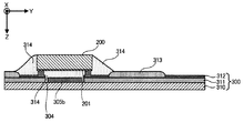
図7は、駆動用集積回路200が取り付けられたフレキシブル回路基板300の、図1に示すY方向に沿った方向の断面図である。
図7に示すように、駆動用集積回路200において、フレキシブル基板300に接着される面、つまり、フレキシブル回路基板300の接着面304に対向する面には、駆動用集積回路200の接地端子と電気的に接続された配線層201が、一様に広がって形成されている。
FIG. 7 is a cross-sectional view of the
As shown in FIG. 7, in the drive integrated
フレキシブル回路基板300は、ポリイミド等で形成されたベース材料310と、ベース材料310上に形成された銅箔311と、第1接続端子群302および第2接続端子群303ならびに配線301を形成するAuメッキ312とから構成されている。また、銅箔311上には、適宜、ソルダーレジスト313が設けられている。
The
駆動用集積回路200は、所定の誘電率を有するアンダーフィル314を接着剤として、フレキシブル基板300の接着面304に接着される。また、アンダーフィル314は、駆動用集積回路200の接地端子等の端子と配線301との接続部を覆うように設けられる。
The drive integrated
図7に示すように、駆動用集積回路200をアンダーフィル314によりフレキシブル基板300の接着面304に接着した状態では、駆動用集積回路200の配線層201と、接着面304に形成されたベタパターンの電源パターン305a,305b,305cとが、アンダーフィル314を介して対向して配置される。したがって、本実施形態においては、フレキシブル回路基板300の電源パターン305a,305b,305cを、いわゆるベタパターンとしたことにより、駆動用集積回路200の接地端子と電気的に接続された配線層201に結合する付加容量が形成されることになる。
As shown in FIG. 7, in a state where the drive integrated
その結果、本実施形態においては、片面配線基板のフレキシブル回路基板300を用いる場合でも、デカップリングコンデンサー素子を付加することなく、集積回路200の接地端子の低インピーダンス化と、配線層201に対する付加容量の結合を実現することができ、電源の安定性を図ることができる。したがって、データ線駆動回路30から画素PIXに対して画像信号D[n]を供給するタイミングで電源電圧が変動した場合でも、短い期間で電源電圧を安定させることができる。また、このように電源電圧を安定させることができるので、画素PIXに対する書き込み時間も短縮することができ、表示むらの発生等を防止して、表示品位を向上させることができる。
As a result, in the present embodiment, even when the
<第2実施形態>
次に、本発明の第2実施形態について図8を参照しつつ説明する。図8は本実施形態におけるフレキシブル回路基板300の一部を示す平面図である。
<Second Embodiment>
Next, the second embodiment of the present invention will be described with reference to FIG. FIG. 8 is a plan view showing a part of the
本実施形態においては、フレキシブル回路基板300の接着面304には、第2接続端子群303に含まれる電源用接続端子のうち接地端子と電気的に接続された面状の接地パターン305dが、接着面304の接続端子が配置される領域を除く全面に亘って形成されている。接地パターンは、いわゆるベタパターンとして形成されている。
In the present embodiment, a
また、本実施形態においては、図示を省略するが、集積回路200において、フレキシブル回路基板300に接着される面、つまり、フレキシブル回路基板300の接着面304に対向する面には、駆動用集積回路200の電源端子と電気的に接続された配線層201が、接着面304に対向する面に形成されている。
Further, in the present embodiment, although not shown, the
したがって、本実施形態においても、駆動用集積回路200をアンダーフィル314により接着面304に接着した状態では、駆動用集積回路200の電源端子に接続された配線層201と、フレキシブル回路基板300の接着面304に形成されたベタパターンの接地パターン305dとが、アンダーフィル314を介して対向して配置される。したがって、本実施形態においては、フレキシブル回路基板300の接地パターン305dを、いわゆるベタパターンとしたことにより、駆動用集積回路200の電源端子と電気的に接続された配線層201に結合する付加容量が形成されることになる。
Therefore, also in the present embodiment, when the drive integrated
その結果、本実施形態においても、片面のフレキシブル回路基板300を用いる場合でも、デカップリングコンデンサー素子を付加することなく、駆動用集積回路200の接地端子の低インピーダンス化と、配線層201に対する付加容量の結合を実現することができ、電源の安定性を図ることができる。したがって、データ線駆動回路30から画素PIXに対して画像信号D[n]を供給するタイミングで電源電圧が変動した場合でも、短い期間で電源電圧を安定させることができる。また、このように電源電圧を安定させることができるので、画素PIXに対する書き込み時間も短縮することができ、表示むらの発生等を防止して、表示品位を向上させることができる。
As a result, also in the present embodiment, even when the one-sided
<変形例>
本発明は、上述した各実施形態に限定されるものではなく、例えば、以下に述べる各種の変形が可能である。また、各実施形態および各変形例を適宜組み合わせてもよいことは勿論である。
<Modification example>
The present invention is not limited to the above-described embodiments, and various modifications described below are possible, for example. Of course, each embodiment and each modification may be combined as appropriate.
(変形例1)
第1形態においては、フレキシブル回路基板300の接着面304に形成するベタパターンの電源パターンを3分割としたが、本発明はこのような態様に限定されるものではなく、電源パターンの分割数あるいは分割の仕方は、駆動用集積回路200のレイアウトに合わせて適宜変更可能である。
(Modification example 1)
In the first embodiment, the power supply pattern of the solid pattern formed on the
(変形例2)
上述した実施形態においては電気光学材料の一例として液晶を取上げたが、それら以外の電気光学材料を用いた電気光学装置にも本発明は適用される。電気光学材料とは、電気信号(電流信号または電圧信号)の供給によって透過率や輝度といった光学的特性が変化する材料である。例えば、有機EL(ElectroLuminescent)、無機ELや発光ポリマーなどの発光素子を用いた表示パネルに対しても上記実施形態と同様に本発明が適用され得る。また、着色された液体と当該液体に分散された白色の粒子とを含むマイクロカプセルを電気光学材料として用いた電気泳動表示パネルに対しても上記実施形態と同様に本発明が適用され得る。さらに、極性が相違する領域ごとに異なる色に塗り分けられたツイストボールを電気光学材料として用いたツイストボールディスプレイパネルに対しても上記実施形態と同様に本発明が適用され得る。黒色トナーを電気光学材料として用いたトナーディスプレイパネル、あるいはヘリウムやネオンなどの高圧ガスを電気光学材料として用いたプラズマディスプレイパネルなど各種の電気光学装置に対しても上記実施形態と同様に本発明が適用され得る。
(Modification 2)
In the above-described embodiment, the liquid crystal is taken up as an example of the electro-optical material, but the present invention is also applied to an electro-optical device using other electro-optical materials. The electro-optical material is a material whose optical characteristics such as transmittance and brightness change depending on the supply of an electric signal (current signal or voltage signal). For example, the present invention can be applied to a display panel using a light emitting element such as an organic EL (ElectroLuminescent), an inorganic EL, or a light emitting polymer, as in the above embodiment. Further, the present invention can be applied to an electrophoresis display panel using microcapsules containing a colored liquid and white particles dispersed in the liquid as an electro-optical material, as in the above embodiment. Further, the present invention can be applied to a twist ball display panel using twist balls painted in different colors for regions having different polarities as an electro-optical material, as in the above embodiment. Similar to the above embodiment, the present invention also applies to various electro-optical devices such as a toner display panel using black toner as an electro-optical material or a plasma display panel using a high-pressure gas such as helium or neon as an electro-optical material. Can be applied.
<応用例>
この発明は、各種の電子機器に利用され得る。図9から図11は、この発明の適用対象となる電子機器の具体的な形態を例示するものである。
<Application example>
The present invention can be used in various electronic devices. 9 to 11 illustrate specific forms of electronic devices to which the present invention is applied.
図9は、電気光学装置を採用した可搬型のパーソナルコンピューターの斜視図である。パーソナルコンピューター2000は、各種の画像を表示する電気光学装置1と、電源スイッチ2001やキーボード2002が設置された本体部2010とを具備する。
FIG. 9 is a perspective view of a portable personal computer using an electro-optical device. The
図10は、携帯電話機の斜視図である。携帯電話機3000は、複数の操作ボタン3001およびスクロールボタン3002と、各種の画像を表示する電気光学装置1とを備える。スクロールボタン3002を操作することによって、電気光学装置1に表示される画面がスクロールされる。本発明はこのような携帯電話機にも適用可能である。
FIG. 10 is a perspective view of the mobile phone. The
図11は、電気光学装置を採用した投射型表示装置(3板式のプロジェクター)4000の構成を示す模式図である。この投射型表示装置4000は、相異なる表示色R、G、Bに各々対応する3個の電気光学装置1(1R,1G,1B)を含んでいる。照明光学系4001は、照明装置(光源)4002からの出射光のうち赤色成分rを電気光学装置1Rに供給し、緑色成分gを電気光学装置1Gに供給し、青色成分bを電気光学装置1Bに供給する。各電気光学装置1は、照明光学系4001から供給される各単色光を表示画像に応じて変調する光変調器(ライトバルブ)として機能する。投射光学系4003は、各電気光学装置1からの出射光を合成して投射面4004に投射する。本発明はこのような液晶プロジェクターにも適用可能である。
FIG. 11 is a schematic view showing the configuration of a projection type display device (three-panel projector) 4000 that employs an electro-optical device. The projection
なお、本発明が適用される電子機器としては、図1、図9から図11に例示した機器のほか、携帯情報端末(PDA:Personal Digital Assistants)が挙げられる。その他にも、デジタルスチルカメラ,テレビ,ビデオカメラ,カーナビゲーション装置,車載用の表示器(インパネ),電子手帳,電子ペーパー,電卓,ワードプロセッサー,ワークステーション,テレビ電話,POS端末が挙げられる。さらに、プリンター,スキャナー,複写機,ビデオプレーヤー,タッチパネルを備えた機器等などが挙げられる。 Examples of the electronic device to which the present invention is applied include devices illustrated in FIGS. 1, 9 to 11, and personal digital assistants (PDAs). Other examples include digital still cameras, televisions, video cameras, car navigation devices, in-vehicle displays (instrument panels), electronic organizers, electronic papers, calculators, word processors, workstations, videophones, and POS terminals. Further, printers, scanners, copiers, video players, devices equipped with touch panels, etc. can be mentioned.
1…電気光学装置、10…画素部、12…走査線、14…データ線、15…VID信号線、16…信号線、17…制御線、20…走査線駆動回路、30…データ線駆動回路、40…制御回路、57…デマルチプレクサー、58…スイッチ、60…液晶素子、62…画素電極、64…コモン電極、66…液晶、70…TFTアレイ基板、70a…画像表示領域、71…配向膜、80…対向基板、81…遮光膜、82…対向電極、83…配向膜、90…引回配線、91…シール材、92…額縁遮光膜、100…電気光学パネル、102…外部回路接続端子、106…上下導通端子、107…上下導通材、200…駆動用集積回路、200a…接着位置、201…配線層、300…フレキシブル回路基板、300a…配線形成面、301…配線、302…第1接続端子群、303…第2接続端子群、304…接着面、305a,305b,305c…電源パターン、305d…接地パターン、310…ベース材料、311…銅箔、312…Auメッキ、313…ソルダーレジスト、314…アンダーフィル、2000…パーソナルコンピューター、3000…携帯電話機、4000…投射型表示装置、B…配線ブロック、CLX…Xクロック信号、CLY…Yクロック信号、D…画像信号、DCLK…ドットクロック信号、DX…X転送開始パルス、DY…Y転送開始パルス、G…走査信号、Hs…水平同期信号、LCCOM…コモン電圧、PIX…画素回路、S1〜S4…選択信号、SW…スイッチング素子。
1 ... Electro-optical device, 10 ... Pixel part, 12 ... Scanning line, 14 ... Data line, 15 ... VID signal line, 16 ... Signal line, 17 ... Control line, 20 ... Scanning line drive circuit, 30 ... Data line drive circuit , 40 ... control circuit, 57 ... demultiplexer, 58 ... switch, 60 ... liquid crystal element, 62 ... pixel electrode, 64 ... common electrode, 66 ... liquid crystal, 70 ... TFT array substrate, 70a ... image display area, 71 ... orientation Film, 80 ... opposed substrate, 81 ... light-shielding film, 82 ... opposed electrode, 83 ... alignment film, 90 ... routing wiring, 91 ... sealing material, 92 ... frame light-shielding film, 100 ... electro-optical panel, 102 ... external circuit connection Terminal, 106 ... Vertical conductive terminal, 107 ... Vertical conductive material, 200 ... Drive integrated circuit, 200a ... Adhesive position, 201 ... Wiring layer, 300 ... Flexible circuit board, 300a ... Wiring forming surface, 301 ... Wiring, 302 ... 1 connection terminal group, 303 ... second connection terminal group, 304 ... adhesive surface, 305a, 305b, 305c ... power supply pattern, 305d ... ground pattern, 310 ... base material, 311 ... copper foil, 312 ... Au plating, 313 ... solder Resist, 314 ... underfill, 2000 ... personal computer, 3000 ... mobile phone, 4000 ... projection display device, B ... wiring block, CLX ... X clock signal, CLY ... Y clock signal, D ... image signal, DCLK ... dot clock Signal, DX ... X transfer start pulse, DY ... Y transfer start pulse, G ... scanning signal, Hs ... horizontal synchronization signal, LCCOM ... common voltage, PIX ... pixel circuit, S1 to S4 ... selection signal, SW ... switching element.
Claims (5)
前記集積回路の前記制御信号を供給する端子と電気的に接続される制御信号用端子を含む第1接続端子群と、前記集積回路の電源端子または接地端子と電気的に接続される電源用接続端子を含む第2接続端子群と、を有するフレキシブル回路基板と、を備え、
前記集積回路は、前記第1接続端子群と前記第2接続端子群との間において、前記フレキシブル回路基板の接着面と接着されており、前記接着面に対向する面に前記電源端子または前記接地端子と電気的に接続された配線層を有し、
前記フレキシブル回路基板の前記接着面には、前記電源用接続端子と電気的に接続された面状のパターンが形成され、
前記配線層と前記面状のパターンは、所定の誘電率を有するアンダーフィルを介して対向し、付加容量を形成する
ことを特徴とする電気光学装置。 An integrated circuit that supplies image and control signals to the electro-optical panel,
A first connection terminal group including a control signal terminal that is electrically connected to a terminal that supplies the control signal of the integrated circuit, and a power supply connection that is electrically connected to the power supply terminal or the ground terminal of the integrated circuit. A second connection terminal group including terminals, and a flexible circuit board having the terminal are provided.
The integrated circuit is adhered to an adhesive surface of the flexible circuit board between the first connection terminal group and the second connection terminal group, and the power supply terminal or the ground is attached to a surface facing the adhesive surface. It has a wiring layer that is electrically connected to the terminals
A planar pattern electrically connected to the power supply connection terminal is formed on the adhesive surface of the flexible circuit board .
An electro-optical device characterized in that the wiring layer and the planar pattern face each other via an underfill having a predetermined dielectric constant to form an additional capacitance.
前記フレキシブル回路基板の前記接着面には、前記電源用接続端子のうち前記電源端子と電気的に接続された面状のパターンが形成されている、
ことを特徴とする請求項1に記載の電気光学装置。 The wiring layer is electrically connected to the ground terminal and is connected to the ground terminal.
A planar pattern is formed on the adhesive surface of the flexible circuit board, which is electrically connected to the power supply terminal among the power supply connection terminals.
The electro-optical device according to claim 1.
ことを特徴とする請求項2に記載の電気光学装置。 The planar pattern is a first planar pattern electrically connected to an analog power supply terminal and a second planar electrical connection to a digital power supply terminal among the power supply terminals. It is divided into a pattern of shape,
The electro-optical device according to claim 2.
前記フレキシブル回路基板の前記接着面には、前記電源用接続端子のうち前記接地端子と電気的に接続された面状のパターンが、前記接着面に形成されている、
ことを特徴とする請求項1に記載の電気光学装置。 The wiring layer is electrically connected to the power supply terminal and is connected to the power supply terminal.
On the adhesive surface of the flexible circuit board, a planar pattern of the power supply connection terminals that is electrically connected to the ground terminal is formed on the adhesive surface.
The electro-optical device according to claim 1.
Priority Applications (2)
| Application Number | Priority Date | Filing Date | Title |
|---|---|---|---|
| JP2016190775A JP6880623B2 (en) | 2016-09-29 | 2016-09-29 | Electro-optics and electronic equipment |
| US15/696,802 US20180088387A1 (en) | 2016-09-29 | 2017-09-06 | Electrooptical device and electronic apparatus |
Applications Claiming Priority (1)
| Application Number | Priority Date | Filing Date | Title |
|---|---|---|---|
| JP2016190775A JP6880623B2 (en) | 2016-09-29 | 2016-09-29 | Electro-optics and electronic equipment |
Publications (3)
| Publication Number | Publication Date |
|---|---|
| JP2018054878A JP2018054878A (en) | 2018-04-05 |
| JP2018054878A5 JP2018054878A5 (en) | 2019-09-19 |
| JP6880623B2 true JP6880623B2 (en) | 2021-06-02 |
Family
ID=61687883
Family Applications (1)
| Application Number | Title | Priority Date | Filing Date |
|---|---|---|---|
| JP2016190775A Active JP6880623B2 (en) | 2016-09-29 | 2016-09-29 | Electro-optics and electronic equipment |
Country Status (2)
| Country | Link |
|---|---|
| US (1) | US20180088387A1 (en) |
| JP (1) | JP6880623B2 (en) |
Families Citing this family (5)
| Publication number | Priority date | Publication date | Assignee | Title |
|---|---|---|---|---|
| JP6605400B2 (en) * | 2016-06-17 | 2019-11-13 | 日立オートモティブシステムズ株式会社 | Electronic control device, vehicle, and electronic control device manufacturing method |
| CN208607473U (en) * | 2018-07-02 | 2019-03-15 | 合肥鑫晟光电科技有限公司 | Array substrate, display panel and display device |
| CN108983477B (en) * | 2018-09-27 | 2021-04-02 | 武汉华星光电半导体显示技术有限公司 | Display module, manufacturing method thereof and electronic device |
| KR102578498B1 (en) * | 2018-10-24 | 2023-09-14 | 삼성디스플레이 주식회사 | Display device |
| WO2021030938A1 (en) * | 2019-08-16 | 2021-02-25 | 京东方科技集团股份有限公司 | Display device and preparation method therefor |
Family Cites Families (3)
| Publication number | Priority date | Publication date | Assignee | Title |
|---|---|---|---|---|
| JP2005027041A (en) * | 2003-07-02 | 2005-01-27 | Renesas Technology Corp | Solid-state imaging unit |
| US8704328B2 (en) * | 2011-06-24 | 2014-04-22 | Fuji Electric Co., Ltd. | High-voltage integrated circuit device |
| KR102275318B1 (en) * | 2015-03-02 | 2021-07-13 | 삼성디스플레이 주식회사 | Image display apparatus |
-
2016
- 2016-09-29 JP JP2016190775A patent/JP6880623B2/en active Active
-
2017
- 2017-09-06 US US15/696,802 patent/US20180088387A1/en not_active Abandoned
Also Published As
| Publication number | Publication date |
|---|---|
| JP2018054878A (en) | 2018-04-05 |
| US20180088387A1 (en) | 2018-03-29 |
Similar Documents
| Publication | Publication Date | Title |
|---|---|---|
| US10802358B2 (en) | Display device with signal lines routed to decrease size of non-display area | |
| US10108057B2 (en) | Electro-optical device and electronic apparatus | |
| JP5024110B2 (en) | Electro-optical device and electronic apparatus | |
| US9875699B2 (en) | Display device | |
| JP6880623B2 (en) | Electro-optics and electronic equipment | |
| JP5239512B2 (en) | Electro-optical device and electronic apparatus | |
| US10319316B2 (en) | Electro-optical device including a plurality of scanning lines | |
| JP2012113088A (en) | Electro-optic device drive circuit, electro-optic device and electronic apparatus | |
| JP2009210674A (en) | Electrooptical device and electronic apparatus | |
| KR102043849B1 (en) | Liquid crystal display device | |
| JP2010108981A (en) | Semiconductor device, electrooptical device, and electronic apparatus | |
| KR100827261B1 (en) | Electro-optical device and electronic apparatus including the same | |
| JP2007219356A (en) | Electro-optical device and electronic apparatus | |
| JP2005181399A (en) | Electrooptic device and electronic equipment | |
| KR102075355B1 (en) | Liquid crystal display device | |
| JP2009205097A (en) | Electro-optical device and electronic equipment | |
| JP2007178524A (en) | Electrooptical apparatus and electronic equipment | |
| JP6354406B2 (en) | Electro-optical device and electronic apparatus | |
| JP2005062353A (en) | Electrooptical panel, electrooptical device, and electronic apparatus | |
| KR20090086151A (en) | Electro-optical device and electronic apparatus | |
| JP2007304388A (en) | Electro-optical device, color filter substrate and electronic apparatus | |
| JP2009042437A (en) | Electro-optical device, driving method therefor, and electronic equipment |
Legal Events
| Date | Code | Title | Description |
|---|---|---|---|
| RD05 | Notification of revocation of power of attorney |
Free format text: JAPANESE INTERMEDIATE CODE: A7425 Effective date: 20180907 |
|
| RD03 | Notification of appointment of power of attorney |
Free format text: JAPANESE INTERMEDIATE CODE: A7423 Effective date: 20181120 |
|
| A521 | Written amendment |
Free format text: JAPANESE INTERMEDIATE CODE: A523 Effective date: 20190809 |
|
| A621 | Written request for application examination |
Free format text: JAPANESE INTERMEDIATE CODE: A621 Effective date: 20190809 |
|
| RD07 | Notification of extinguishment of power of attorney |
Free format text: JAPANESE INTERMEDIATE CODE: A7427 Effective date: 20200803 |
|
| A977 | Report on retrieval |
Free format text: JAPANESE INTERMEDIATE CODE: A971007 Effective date: 20200828 |
|
| A131 | Notification of reasons for refusal |
Free format text: JAPANESE INTERMEDIATE CODE: A131 Effective date: 20200908 |
|
| A521 | Written amendment |
Free format text: JAPANESE INTERMEDIATE CODE: A523 Effective date: 20201014 |
|
| TRDD | Decision of grant or rejection written | ||
| A01 | Written decision to grant a patent or to grant a registration (utility model) |
Free format text: JAPANESE INTERMEDIATE CODE: A01 Effective date: 20210406 |
|
| A61 | First payment of annual fees (during grant procedure) |
Free format text: JAPANESE INTERMEDIATE CODE: A61 Effective date: 20210419 |
|
| R150 | Certificate of patent or registration of utility model |
Ref document number: 6880623 Country of ref document: JP Free format text: JAPANESE INTERMEDIATE CODE: R150 |