以下、添付された図面を参照して各実施例を詳しく説明する。各実施例の説明において、各層(膜)、領域、パターンまたは構造物が、基板、各層(膜)、領域、パッドまたはパターンの「上」または「下」に形成されると記載される場合、「上」と「下」は、直接または他の層を介して形成されるものも含む。また、各層の上または下に対する基準は、図面を基準に説明する。
Hereinafter, each embodiment will be described in detail with reference to the attached drawings. When it is stated in the description of each embodiment that each layer (membrane), region, pattern or structure is formed "above" or "below" the substrate, each layer (membrane), region, pad or pattern. "Upper" and "lower" also include those formed directly or through other layers. The criteria for the top or bottom of each layer will be described with reference to the drawings.
以下、添付された図面を参照して実施例に係る光学レンズおよびこれを備えた光源モジュールを説明する。
Hereinafter, an optical lens according to an embodiment and a light source module provided with the optical lens will be described with reference to the attached drawings.
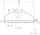
図1は第1実施例に係る光学レンズの平面図であり、図2は図1の光学レンズの底面図であり、図3は図1の光学レンズのX軸方向の第1側面図であり、図4は図1の光学レンズのY軸方向の第2側面図であり、図5は図1の光学レンズのA‐A側断面図であり、図6は図1の光学レンズのB‐B側断面図である。
1 is a plan view of the optical lens according to the first embodiment, FIG. 2 is a bottom view of the optical lens of FIG. 1, and FIG. 3 is a first side view of the optical lens of FIG. 1 in the X-axis direction. 4 is a second side view of the optical lens of FIG. 1 in the Y-axis direction, FIG. 5 is a sectional view of the optical lens of FIG. 1 on the AA side, and FIG. 6 is a B- of the optical lens of FIG. It is a B side sectional view.
図1〜図6に示すように、光学レンズ300は、底面310、前記底面310の中心部に凹状のリセス315、前記底面310および前記リセス315の上に曲面を有する第1出射面330を含む。前記光学レンズ300において前記リセス315の表面は入射面320からなることができる。
As shown in FIGS. 1 to 6, the optical lens 300 includes a bottom surface 310, a recessed recess 315 at the center of the bottom surface 310, and a first exit surface 330 having a curved surface on the bottom surface 310 and the recess 315. .. In the optical lens 300, the surface of the recess 315 can consist of an incident surface 320.
前記光学レンズ300は、第1軸方向(X)の第1長さ(D1)と前記第2軸方向(Y)の第2長さ(D2)が異なる。前記第1軸方向は、前記第2軸方向と直交する方向であり、前記第1、2軸方向と直交する垂直方向は第3軸方向(Z)である。前記第1長さ(D1)はX軸方向の最大長さとして、X軸方向の相互反対側表面の間の間隔である。前記第2長さ(D2)はY軸方向の最大長さとして、Y軸方向の相互反対側表面の間の間隔である。前記光学レンズ300において、第1長さ(D1)と第2長さ(D2)はX軸とY軸方向の最大長さである。前記光学レンズ300において、第1長さ(D1)と第2長さ(D2)は底面310のX軸とY軸方向の長さである。前記光学レンズ300において、第1長さ(D1)と第2長さ(D2)は、前記第1出射面330のX軸とY軸方向の最大長さである。前記第1長さ(D1)は、X軸方向において側面突出部360を除いた第2出射面335の最大長さである。前記第1長さ(D1)と第2長さ(D2)は、D1<D2の関係を有することができる。前記第1長さ(D1)と第2長さ(D2)の差は、0.5mm以上、例えば1mm以上である。前記第1長さ(D1)と第2長さ(D2)の差は1mm以上、例えば1mm〜3.5mmの範囲を有することができる。前記第1長さ(D1)と第2長さ(D2)の差は3.5mm以下である。前記第1長さ(D1)と第2長さ(D2)の差は、前記第2長さ(D2)の10%以下である。前記第1長さ(D1)と第2長さ(D2)の差が1mm未満の場合、X軸方向とY軸方向の輝度分布の差が微小で、3.5mmを超える場合、両軸方向の輝度分布の差が過大となるか、いずれか1つの軸方向の輝度分布が低すぎることになる問題がある。実施例に係る光学レンズ300は、Y軸方向の長さ(D2)がX軸方向の長さ(D1)より長い長さを有するので、Y軸を基準に、X軸方向への光出射面積がより増加することになる。
The optical lens 300 has a different first length (D1) in the first axial direction (X) and a second length (D2) in the second axial direction (Y). The first axial direction is a direction orthogonal to the second axial direction, and the vertical direction orthogonal to the first and second axial directions is the third axial direction (Z). The first length (D1) is the maximum length in the X-axis direction, which is the distance between the surfaces on opposite sides in the X-axis direction. The second length (D2) is the maximum length in the Y-axis direction, which is the distance between the surfaces on opposite sides in the Y-axis direction. In the optical lens 300, the first length (D1) and the second length (D2) are the maximum lengths in the X-axis and Y-axis directions. In the optical lens 300, the first length (D1) and the second length (D2) are the lengths of the bottom surface 310 in the X-axis and Y-axis directions. In the optical lens 300, the first length (D1) and the second length (D2) are the maximum lengths of the first exit surface 330 in the X-axis and Y-axis directions. The first length (D1) is the maximum length of the second exit surface 335 excluding the side protrusion 360 in the X-axis direction. The first length (D1) and the second length (D2) can have a relationship of D1 <D2. The difference between the first length (D1) and the second length (D2) is 0.5 mm or more, for example, 1 mm or more. The difference between the first length (D1) and the second length (D2) can have a range of 1 mm or more, for example, 1 mm to 3.5 mm. The difference between the first length (D1) and the second length (D2) is 3.5 mm or less. The difference between the first length (D1) and the second length (D2) is 10% or less of the second length (D2). When the difference between the first length (D1) and the second length (D2) is less than 1 mm, the difference in brightness distribution between the X-axis direction and the Y-axis direction is small, and when it exceeds 3.5 mm, both axial directions. There is a problem that the difference in the luminance distributions of the above is excessive, or the luminance distribution in any one of the axial directions is too low. Since the optical lens 300 according to the embodiment has a length (D2) in the Y-axis direction longer than the length (D1) in the X-axis direction, the light emitting area in the X-axis direction with reference to the Y-axis. Will increase more.
前記光学レンズ300は、透光性材料を含むことができる。前記光学レンズ300は、ポリカーボネート(PC)、ポリメタクリル酸メチル(PMMA)、シリコンまたはエポキシ樹脂、またはグラス(Glass)のうち少なくとも1つを含むことができる。前記光学レンズ300は、屈折率が1.7以下、例えば1.4〜1.7範囲の透明材料を含むことができる。前記光学レンズ300は、透光性材質のレンズ本体を含むことができる。
The optical lens 300 can include a translucent material. The optical lens 300 can include at least one of polycarbonate (PC), polymethyl methacrylate (PMMA), silicone or epoxy resin, or glass. The optical lens 300 can include a transparent material having a refractive index of 1.7 or less, for example, in the range of 1.4 to 1.7. The optical lens 300 can include a lens body made of a translucent material.
前記光学レンズ300の底面310は、前記レンズ本体の底からなることができる。前記底面310は、第1出射面310の反対側面からなることができる。前記底面310の面積は、前記第1出射面310の表面積より小さい面積を有することができる。前記底面310において、X軸方向の長さ(D1)とY軸方向の長さ(D2)は、D1<D2の関係を有することができる。前記底面310において、長さの比率D1:D2は1:1.01〜1:1.1の範囲を有することができる。前記底面310は外枠形状が楕円形状を有することができる。前記底面310は、外枠ラインの形状が前記底の中心(P0)を通るX軸方向を基準に対称する形状を有し、前記Y軸方向を基準に対称する形状を有することができる。前記底の中心(P0)を基準に第1軸(X)方向に水平な第1直線はX0で、第2軸(Y)方向に水平な第2直線はY0でる。前記底の中心(P0)は、直線X0とY0が交差する地点である。前記底面310と前記リセス315のボトムビュー形状は、相互異なる楕円形状、例えば、相互異なる軸方向の長さが長い楕円形状を有することができる。
The bottom surface 310 of the optical lens 300 can consist of the bottom surface of the lens body. The bottom surface 310 can consist of the opposite side surface of the first exit surface 310. The area of the bottom surface 310 can be smaller than the surface area of the first exit surface 310. In the bottom surface 310, the length in the X-axis direction (D1) and the length in the Y-axis direction (D2) can have a relationship of D1 <D2. On the bottom surface 310, the length ratio D1: D2 can have a range of 1: 1.01 to 1: 1.1. The bottom surface 310 may have an elliptical outer frame shape. The bottom surface 310 may have a shape in which the shape of the outer frame line is symmetrical with respect to the X-axis direction passing through the center (P0) of the bottom, and may have a shape symmetrical with respect to the Y-axis direction. The first straight line horizontal in the first axis (X) direction with respect to the center (P0) of the bottom is X0, and the second straight line horizontal in the second axis (Y) direction is Y0. The center (P0) of the bottom is a point where the straight lines X0 and Y0 intersect. The bottom view shapes of the bottom surface 310 and the recess 315 can have different elliptical shapes, for example, different elliptical shapes having different axial lengths.
前記光学レンズ300は、下部中心に凹状のリセス315を含むことができる。前記底面310は、中心領域に凹状のリセス315を有することができる。前記リセス315の表面は、入射面320からなることができる。前記光学レンズ300は、前記リセス315の底の中心(P0)に対して垂直なZ軸方向を中心軸(Z0)と定義することができる。前記リセス315の底の中心(P0)は、光学レンズ300の下部中心または前記底面310の中心であり、基準点と定義することができる。前記底面310は、リセス315の周りに配置される。
The optical lens 300 can include a recessed recess 315 in the center of the lower part. The bottom surface 310 can have a concave recess 315 in the central region. The surface of the recess 315 can consist of an incident surface 320. In the optical lens 300, the Z-axis direction perpendicular to the center (P0) of the bottom of the recess 315 can be defined as the central axis (Z0). The center (P0) of the bottom of the recess 315 is the center of the lower part of the optical lens 300 or the center of the bottom 310, and can be defined as a reference point. The bottom surface 310 is arranged around the recess 315.
前記底面310は、前記底の中心(P0)に対してX軸方向に水平な第1直線(X0)およびY軸方向に水平な第2直線(Y0)に対して傾斜した面または曲面を含むことができ、或いは傾斜した面と曲面を両方とも含むことができる。前記底面310において、前記リセス315に隣接した領域はフラットであり、外周エッジに隣接した領域は傾斜した面からなることができる。前記底面310は傾斜した面または曲面を含むことができ、前記傾斜した面または曲面は、前記リセス315または底の中心(P0)から外周エッジに行くほど高い高さを有することができる。前記リセス315は、前記底面310の中心領域から上方に凹状または陥没した形態を有する。前記リセス315は、第1出射面310方向に凹んだ領域からなることができる。
The bottom surface 310 includes a surface or curved surface inclined with respect to a first straight line (X0) horizontal to the center (P0) of the bottom in the X-axis direction and a second straight line (Y0) horizontal to the Y-axis direction. It can be, or it can include both sloping surfaces and curved surfaces. On the bottom surface 310, the region adjacent to the recess 315 is flat and the region adjacent to the outer peripheral edge can consist of an inclined surface. The bottom surface 310 can include an inclined surface or curved surface, and the inclined surface or curved surface can have a height toward the outer peripheral edge from the recess 315 or the center (P0) of the bottom. The recess 315 has a concave or recessed form upward from the central region of the bottom surface 310. The recess 315 can consist of a region recessed in the direction of the first exit surface 310.
前記光学レンズ300の底面310は、リセス315に隣接した第1エッジ23および第2出射面335に隣接した第2エッジ25を含む。前記第1エッジ23は、前記入射面320と前記底面310との間の境界領域であり、光学レンズ300の低点領域を含むことができる。前記第1エッジ23は、前記底面310の領域のうち最も低い地点を含むことができる。前記第1エッジ23の位置は、水平な第1直線(X0)および第2直線(Y0)を基準に第2エッジ25の位置より低く配置される。前記第1エッジ23は、前記入射面320の下部周りをカバーすることができる。前記第2エッジ25は、前記底面310の外周領域または前記第2出射面335の下部領域となることができる。前記第2エッジ25は、前記底面310と前記第2出射面335との間の境界領域からなることができる。
The bottom surface 310 of the optical lens 300 includes a first edge 23 adjacent to the recess 315 and a second edge 25 adjacent to the second exit surface 335. The first edge 23 is a boundary region between the incident surface 320 and the bottom surface 310, and may include a low point region of the optical lens 300. The first edge 23 may include the lowest point in the region of the bottom surface 310. The position of the first edge 23 is lower than the position of the second edge 25 with reference to the horizontal first straight line (X0) and second straight line (Y0). The first edge 23 can cover the lower portion of the incident surface 320. The second edge 25 can be an outer peripheral region of the bottom surface 310 or a lower region of the second exit surface 335. The second edge 25 can consist of a boundary region between the bottom surface 310 and the second exit surface 335.
前記第1エッジ23は、前記底面310の内側領域または前記入射面320との境界ラインからなることができる。前記第2エッジ25は、前記底面310の外側領域または第2出射面335との境界ラインからなることができる。前記第1エッジ23は、内側角または曲面を含むことができる。前記第2エッジ25は、外側角または曲面を含むことができる。前記第1エッジ23と第2エッジ25は、前記底面310の両端部からなることができる。前記第1エッジ23は、ボトムビュー形状が円形状または楕円形状を有することができ、前記第2エッジ25は、ボトムビュー形状が円形状または楕円形状を有することができる。
The first edge 23 can consist of an inner region of the bottom surface 310 or a boundary line with the incident surface 320. The second edge 25 can consist of an outer region of the bottom surface 310 or a boundary line with a second exit surface 335. The first edge 23 may include an inner corner or a curved surface. The second edge 25 may include an outer corner or a curved surface. The first edge 23 and the second edge 25 can consist of both ends of the bottom surface 310. The first edge 23 can have a circular or elliptical bottom view shape, and the second edge 25 can have a circular or elliptical bottom view shape.
前記底面310は、前記第1エッジ23に近いほど、前記水平な第1直線(X0)および第2直線(Y0)との間隔が狭くなる。前記底面310は、前記第1エッジ23から離れるほど、前記水平な第1直線(X0)および第2直線(Y0)との間隔が大きくなる。前記底面310において、前記第2エッジ25は、前記第1直線(X0)および第2直線(Y0)との間隔が最大であり、前記第1エッジ23は、前記第1直線(X0)および第2直線(Y0)との間の間隔が最小である。前記底面310は、前記第1エッジ23と前記第2エッジ25との間に傾斜した面または曲面を含み、または傾斜した面と曲面を両方とも含むことができる。前記底面310は、前記第1直線(X0)および第2直線(Y0)を基準に外側に行くほど遠くなることで、前記リセス315から見るときは全反射面となることができる。例えば、前記リセス315内で前記リセス315の底の上に任意の光源が配置された場合、前記底面310は傾斜した面を提供することができる。前記底面310は、前記リセス315を介して入射する光を反射させることで、光の損失を減らすことができる。また前記入射面320を経ることなく底面310に直接入射する光を除去することができる。前記光学レンズ300は、入射面320を介して反射面310に入射した光の光量を増加させることができ、指向角分布を改善させることができる。
The closer the bottom surface 310 is to the first edge 23, the narrower the distance between the horizontal first straight line (X0) and the second straight line (Y0). The distance between the bottom surface 310 and the horizontal first straight line (X0) and the second straight line (Y0) increases as the distance from the first edge 23 increases. In the bottom surface 310, the second edge 25 has the maximum distance between the first straight line (X0) and the second straight line (Y0), and the first edge 23 has the first straight line (X0) and the first straight line (X0). The distance between the two straight lines (Y0) is the smallest. The bottom surface 310 may include an inclined surface or curved surface between the first edge 23 and the second edge 25, or may include both an inclined surface and a curved surface. The bottom surface 310 can be a total reflection surface when viewed from the recess 315 by becoming farther outward from the first straight line (X0) and the second straight line (Y0). For example, if any light source is placed on the bottom of the recess 315 within the recess 315, the bottom 310 can provide an inclined surface. The bottom surface 310 can reduce the loss of light by reflecting the light incident on the recess 315. Further, the light directly incident on the bottom surface 310 can be removed without passing through the incident surface 320. The optical lens 300 can increase the amount of light incident on the reflecting surface 310 via the incident surface 320, and can improve the directivity angle distribution.
前記底面310が前記リセス315の第1エッジ23に隣接するほどより低くなることになる。前記第1エッジ23に隣接した底面310は、第1直線(X0)および第2直線(Y0)に段々近くなる。これによって、前記底面310の面積はフラットな底に比べて増加することになる。前記リセス315の入射面320の面積は、前記底面310が低くなっただけより広くなる。前記リセス315の深さ(図5のD8)は、前記第1エッジ23からの垂直な高さになるので、より深くなることになる。前記底面310の面積が増加することで、反射面積を増加させることができる。前記リセス315の底はさらに低くなるので、底の面積を増加させることができる。
The bottom surface 310 becomes lower as it is adjacent to the first edge 23 of the recess 315. The bottom surface 310 adjacent to the first edge 23 gradually approaches the first straight line (X0) and the second straight line (Y0). As a result, the area of the bottom surface 310 is increased as compared with the flat bottom surface. The area of the incident surface 320 of the recess 315 becomes larger as the bottom surface 310 becomes lower. The depth of the recess 315 (D8 in FIG. 5) becomes deeper because it is a vertical height from the first edge 23. By increasing the area of the bottom surface 310, the reflection area can be increased. Since the bottom of the recess 315 is even lower, the area of the bottom can be increased.
前記底面310の第1エッジ23は、前記リセス315の底と水平な第1直線(X0)および第2直線(Y0)上に配置され、前記第2エッジ25は、前記第1直線(X0)および第2直線(Y0)から所定間隔で離隔する。前記第2エッジ25と前記第1直線(X0)または第2直線(Y0)との間の間隔は、入射面320の下部領域22に入射した光を反射させるように傾斜した面を提供できる距離である。前記入射面320の下部領域22は、前記第2エッジ25に水平な線が交差する入射面320の下部地点と第1エッジ23との間の領域でる。
The first edge 23 of the bottom surface 310 is arranged on a first straight line (X0) and a second straight line (Y0) horizontal to the bottom of the recess 315, and the second edge 25 is the first straight line (X0). And separated from the second straight line (Y0) at predetermined intervals. The distance between the second edge 25 and the first straight line (X0) or second straight line (Y0) is a distance that can provide an inclined surface that reflects light incident on the lower region 22 of the incident surface 320. Is. The lower region 22 of the incident surface 320 is a region between the lower point of the incident surface 320 and the first edge 23 where a horizontal line intersects the second edge 25.
前記第2エッジ25と前記第1直線(X0)または第2直線(Y0)との間の間隔は500μm以下、例えば450μm以下である。前記第2エッジ25と前記第1直線(X0)または第2直線(Y0)との間の間隔は200μm〜450μmの範囲を有することができる。ここで、前記第2エッジ25と前記第1直線(X0)または第2直線(Y0)との間の間隔が前記範囲より小さい場合、前記第2出射面335の底点位置が低くなって前記第2出射面335に放出された光の間の干渉問題が発生し、前記範囲より大きい場合、前記第2出射面335の高点位置が高くなって第1出射面330の曲率が変更される問題が発生し、光学レンズ300の厚さ(D5)が増加する問題がある。
The distance between the second edge 25 and the first straight line (X0) or the second straight line (Y0) is 500 μm or less, for example 450 μm or less. The distance between the second edge 25 and the first straight line (X0) or the second straight line (Y0) can have a range of 200 μm to 450 μm. Here, when the distance between the second edge 25 and the first straight line (X0) or the second straight line (Y0) is smaller than the above range, the bottom point position of the second exit surface 335 becomes lower. If an interference problem occurs between the light emitted to the second exit surface 335 and is larger than the above range, the high point position of the second exit surface 335 becomes higher and the curvature of the first exit surface 330 is changed. There is a problem that a problem occurs and the thickness (D5) of the optical lens 300 increases.
前記光学レンズ300の底面310は、ベジェ(Bezier)曲線を有する曲面に形成される。前記底面310の曲線は、スプライン(Spline)、例えばキュービック(cubic)、B‐スプライン、T‐スプラインで具現することができる。前記底面310の曲線は、ベジェ曲線(Bezier curve)で具現することができる。
The bottom surface 310 of the optical lens 300 is formed on a curved surface having a Bezier curve. The curve of the bottom surface 310 can be embodied by splines, such as cubic, B-spline, T-spline. The curve of the bottom surface 310 can be embodied by a Bezier curve.
前記光学レンズ300の底面310には、複数の支持突起350を含むことができる。前記複数の支持突起350は、前記光学レンズ300の底面310から下方に突出して前記光学レンズ300を支持することになる。図2に示すように、複数の支持突起350は底の中心(P0)から同一距離に配置される。他の例として、複数の支持突起350のうち少なくとも1つは、前記底の中心(P0)から異なる距離を持って配置されてもよい。前記複数の支持突起350は、X軸方向に配列された突起間の間隔(D13)が第2軸(Y)方向に配列された突起間の間隔(D12)より大きい。前記D13はD12の1.5倍以上、例えば2倍以上である。前記複数の支持突起350のうち間隔(D12)は光学レンズが配列される回路基板の幅方向であるので、回路基板の幅を増加さることなく光学レンズ300を安定的に支持することができる。
The bottom surface 310 of the optical lens 300 can include a plurality of support protrusions 350. The plurality of support protrusions 350 project downward from the bottom surface 310 of the optical lens 300 to support the optical lens 300. As shown in FIG. 2, the plurality of support protrusions 350 are arranged at the same distance from the center (P0) of the bottom. As another example, at least one of the plurality of support protrusions 350 may be arranged at different distances from the center (P0) of the bottom. In the plurality of support protrusions 350, the distance between the protrusions arranged in the X-axis direction (D13) is larger than the distance between the protrusions arranged in the second axis (Y) direction (D12). The D13 is 1.5 times or more, for example, twice or more that of D12. Since the interval (D12) of the plurality of support protrusions 350 is in the width direction of the circuit board on which the optical lenses are arranged, the optical lens 300 can be stably supported without increasing the width of the circuit board.
図2のように、前記底面310のボトムビュー形状は楕円形状を含むことができる。前記底面310の長さは、X軸方向の第1長さ(D1)とY軸方向の第2長さ(D2)が異なる。前記第1長さ(D1)は底面310のX軸方向の長さであり、第2長さ(D2)は底面320のY軸方向の長さである。前記第1長さ(D1)は第1出射面330のX軸方向への最大長さであり、第2長さ(D2)は第1出射面330のY軸方向への最大長さである。前記D1は光学レンズのX軸方向の最大長さであり、D2はY軸方向の最大長さである。前記第2長さ(D2)と第1長さ(D1)は、D2>D1の関係を有することができる。前記D2/D1の比率は101%以上、例えば101%〜110%の範囲を有することができる。前記D2はD1より0.5mm以上、例えば1mm以上である。前記D2はD1より1mm以上、例えば1mm〜3.5mmの範囲の長い長さを有することができる。前記長さの比率(D1:D2)は1:1.01〜1:1.1の範囲を有することができる。前記光学レンズ300の第1出射面330がY軸方向に最大長さを有することになるので、Y軸方向を基準に直交するX軸方向または対角線方向への出射面積を増加させることができる。
As shown in FIG. 2, the bottom view shape of the bottom surface 310 may include an elliptical shape. The length of the bottom surface 310 is different from the first length (D1) in the X-axis direction and the second length (D2) in the Y-axis direction. The first length (D1) is the length of the bottom surface 310 in the X-axis direction, and the second length (D2) is the length of the bottom surface 320 in the Y-axis direction. The first length (D1) is the maximum length of the first exit surface 330 in the X-axis direction, and the second length (D2) is the maximum length of the first exit surface 330 in the Y-axis direction. .. D1 is the maximum length of the optical lens in the X-axis direction, and D2 is the maximum length in the Y-axis direction. The second length (D2) and the first length (D1) can have a relationship of D2> D1. The D2 / D1 ratio can have a ratio of 101% or more, for example, 101% to 110%. The D2 is 0.5 mm or more, for example, 1 mm or more from D1. The D2 can have a longer length than D1 by 1 mm or more, for example, in the range of 1 mm to 3.5 mm. The length ratio (D1: D2) can range from 1: 1.01 to 1: 1.1. Since the first exit surface 330 of the optical lens 300 has a maximum length in the Y-axis direction, the emission area in the X-axis direction or the diagonal direction orthogonal to the Y-axis direction can be increased.
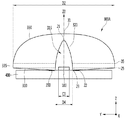
図2のように、前記リセス315の底の形状は楕円形状を含むことができる。図3〜図6のように、前記リセス315は、側断面が鐘(bell)形状、砲弾(shell)形状または楕円形状を含むことができる。前記リセス315は上方に行くほど幅が段々狭くなる形状を有することができる。前記リセス315は、底の周りの第1エッジ23から上端の第1頂点21に向かって徐々に収束される形状を有することができる。前記リセス315のボトムビューが楕円形状である場合、前記第1頂点21に向かって直径が徐々に減少することになる。前記リセス315は、中心軸(Z0)を基準にX軸方向に対称またはY軸方向に対称する形状に提供されてもよい。前記入射面320の第1頂点21はドット形状またはライン形状に提供されてもよい。
As shown in FIG. 2, the shape of the bottom of the recess 315 can include an elliptical shape. As shown in FIGS. 3 to 6, the recess 315 may include a bell-shaped, shell-shaped or oval-shaped side cross section. The recess 315 can have a shape in which the width gradually narrows toward the upper side. The recess 315 can have a shape that gradually converges from the first edge 23 around the bottom to the first apex 21 at the top. When the bottom view of the recess 315 is elliptical, the diameter gradually decreases toward the first apex 21. The recess 315 may be provided in a shape symmetrical in the X-axis direction or in the Y-axis direction with respect to the central axis (Z0). The first apex 21 of the incident surface 320 may be provided in a dot shape or a line shape.
前記リセス315の底の長さは、X軸方向の第3長さ(D3)はY軸方向の第4長さ(D4)と異なってもよい。例えば、X軸方向の第3長さ(D3)はY軸方向の第4長さ(D4)より大きい。前記リセス315の底の長さはD3>D4の関係を満足し、その差は0.5mm〜5mm、例えば1mm〜2mmの範囲の差を有することができる。前記第3長さ(D3)は第4長さ(D4)の4倍以下、例えば2倍以下である。前記リセス315の底において、第3、4長さ(D3、D4)の比率(D4:D3)は1:1.1〜1:2の範囲の差を有することができる。このようなリセス315の底の長さの比率によって、Y軸の長さに直交するY軸方向および対角線方向への輝度分布を改善させることができる。
Regarding the length of the bottom of the recess 315, the third length (D3) in the X-axis direction may be different from the fourth length (D4) in the Y-axis direction. For example, the third length (D3) in the X-axis direction is larger than the fourth length (D4) in the Y-axis direction. The bottom length of the recess 315 satisfies the relationship D3> D4, and the difference can have a difference in the range of 0.5 mm to 5 mm, for example 1 mm to 2 mm. The third length (D3) is four times or less, for example, twice or less the fourth length (D4). At the bottom of the recess 315, the ratio (D4: D3) of the third and fourth lengths (D3, D4) can have a difference in the range 1: 1.1 to 1: 2. Such a ratio of the bottom lengths of the recess 315 can improve the luminance distribution in the Y-axis direction and the diagonal direction orthogonal to the length of the Y-axis.
前記リセス315の底において、第3、4長さ(D3、D4)は、光源、すなわち後述される発光素子が挿入され得る幅を有することができる。前記リセス315の底の長さ(D3、D4)は、発光素子の幅の3倍以下、例えば2.5倍以下である。前記リセス315の底の長さ(D3、D4)は、前記発光素子の幅または一辺の長さの1.2倍〜2.5倍の範囲であり、前記範囲より小さい場合、発光素子の挿入が不容易であり、前記範囲より大きい場合、前記発光素子と第1エッジ23との間の領域を介した光損失または光干渉を起こすことがある。
At the bottom of the recess 315, the third and fourth lengths (D3, D4) can have a width into which a light source, i.e. a light emitting element described below, can be inserted. The bottom length (D3, D4) of the recess 315 is 3 times or less, for example 2.5 times or less the width of the light emitting element. The bottom length (D3, D4) of the recess 315 is in the range of 1.2 times to 2.5 times the width of the light emitting element or the length of one side, and if it is smaller than the range, the light emitting element is inserted. Is difficult, and if it is larger than the above range, light loss or light interference may occur through the region between the light emitting element and the first edge 23.
前記底面310において、支持突起350はD12<D13の関係を有する場合、D12>D4の関係を有することができ、D13>D3の関係を有することができる。D12/D4の比率はg1であり、D13/D3の比率はg2である場合、g1<g2の関係を有することができる。これは、X軸方向に配列された光学レンズ300が回路基板の上に安定的に固定および支持さされて光損失を減らすことができる。
In the bottom surface 310, when the support projection 350 has a relationship of D12 <D13, it can have a relationship of D12> D4 and can have a relationship of D13> D3. When the ratio of D12 / D4 is g1 and the ratio of D13 / D3 is g2, the relationship of g1 <g2 can be obtained. This allows the optical lenses 300 arranged in the X-axis direction to be stably fixed and supported on the circuit board to reduce light loss.
実施例に係る光学レンズ300は、底面310または第1出射面330の長さD2/D1の比率はaであり、前記リセス315の長さD3/D4の比率がbである場合、a<bの関係を有することができる。前記D2/D1の比率は第1出射面330における長/短長さの比率であり、D3/D4の比率はリセス315の底における長/短長さの比率である。前記bはaの110%以上、例えば110%〜140%の範囲または120%〜160%の範囲で提供される。前記bはaの1.1倍以上、例えば1.1倍〜1.4倍の範囲または1.2倍〜1.6倍の範囲で提供される。前記リセス315の底において、第1、2軸方向の長さの差は、前記底面310または第1出射面330の第1、2軸方向の長さの差と同一であってもよく異なってもよい。このような非対称形状の光学レンズにおいて前記リセス315の入射面320の面積が対称形状のレンズよりX軸方向に広く提供されるので、光をY軸方向により広く拡散させて提供することができる。これによって、光学レンズ300は、外形的な長さの差によってY軸方向の輝度分布を確保することができ、輝度分布の側面で前記リセス315によってX軸方向および角領域に広く拡散させることができる。これによって、前記光学レンズ300が配列された光源モジュールのバーの個数を2個以下、例えば1個に減らすことができ、バックライトユニットにおける上下コーナー部の輝度分布を改善させることができる。
In the optical lens 300 according to the embodiment, when the ratio of the lengths D2 / D1 of the bottom surface 310 or the first exit surface 330 is a and the ratio of the lengths D3 / D4 of the recess 315 is b, a <b. Can have a relationship of. The D2 / D1 ratio is the length / short length ratio on the first exit surface 330, and the D3 / D4 ratio is the length / short length ratio at the bottom of the recess 315. The b is provided in an amount of 110% or more of a, for example, 110% to 140% or 120% to 160%. The b is provided in a range of 1.1 times or more, for example, 1.1 times to 1.4 times or 1.2 times to 1.6 times a. At the bottom of the recess 315, the difference in length in the first and second axial directions may be the same as the difference in length in the first and second axial directions of the bottom surface 310 or the first exit surface 330. May be good. In such an asymmetrical optical lens, the area of the incident surface 320 of the recess 315 is provided wider in the X-axis direction than in the symmetrical lens, so that light can be diffused and provided more widely in the Y-axis direction. As a result, the optical lens 300 can secure the luminance distribution in the Y-axis direction due to the difference in external length, and can be widely diffused in the X-axis direction and the angular region by the recess 315 on the side surface of the luminance distribution. it can. As a result, the number of bars of the light source module in which the optical lens 300 is arranged can be reduced to two or less, for example, one, and the brightness distribution at the upper and lower corners of the backlight unit can be improved.
図5および図6のように、前記入射面320は、前記底面310のセンター領域から上方に膨らんだ曲面を有し、前記リセス315の周り面または内部表面ある。前記入射面320は、前記リセス315の底の中心(P0)との距離が上方に行くほど遠くなる。前記入射面320は凸状の曲面で提供されるので、全領域で光を屈折させることができる。前記入射面320の下部領域22は、前記第2出射面335より低い位置に配置され、直接または間接的に光が入射される。前記入射面320の下部領域22は、前記リセス315の底から反射された光が入射される。前記入射面320は、ベジェ(Bezier)曲線を有する回転体からなることができる。前記入射面320の曲線は、スプライン(Spline)、例えばキュービック(cubic)、B‐スプライン、T‐スプラインで具現することができる。前記入射面320の曲線は、ベジェ曲線(Bezier curve)で具現することができる。
As shown in FIGS. 5 and 6, the incident surface 320 has a curved surface that bulges upward from the center region of the bottom surface 310, and is a peripheral surface or an internal surface of the recess 315. The incident surface 320 becomes farther as the distance from the center (P0) of the bottom of the recess 315 increases. Since the incident surface 320 is provided by a convex curved surface, light can be refracted in the entire region. The lower region 22 of the incident surface 320 is arranged at a position lower than the second exit surface 335, and light is directly or indirectly incident. Light reflected from the bottom of the recess 315 is incident on the lower region 22 of the incident surface 320. The incident surface 320 can consist of a rotating body having a Bezier curve. The curve of the incident surface 320 can be embodied by splines, such as cubic, B-spline, T-spline. The curve of the incident surface 320 can be embodied by a Bezier curve.
図5および図6のように、光学レンズ300は第1出射面330を含むことができる。前記第1出射面330は、レンズ本体を基準に前記リセス315および前記底面310の反対側面からなることができる。前記第1出射面330は、前記入射面320および前記底面310の反対側面からなることができる。前記第1出射面330は曲面を含む。前記第1出射面330は中心軸(Z0)に対応する地点が第2頂点31となることができ、前記第2頂点31はレンズ本体の頂点となることができる。前記第1出射面330は上方に膨らんだ曲面を含むことができる。前記第1出射面330は全領域が曲面、例えば相互異なる正の曲率を有する曲面に形成される。前記第1出射面330は、前記中心軸(Z0)を基準に軸対称形状、例えばX軸またはY軸対称形状を有することができる。前記第2出射面335において、前記第2頂点31に隣接したセンター側第1領域A1、A2は負の曲率を持たなくてもよい。前記第2出射面335において、前記第2頂点31に隣接した第1領域A1、A2は、相互異なる正の曲率半径を有することができる。前記第1領域A1、A2の外側サイド領域である第2領域A3、A4は、相互異なる曲率半径を有する曲面に形成される。前記第1領域A1、A2のうちA1領域は、前記第1出射面330において中心軸(Z0)を基準にY軸方向に延長され、Z軸方向に前記リセス315とオーバーラップする領域であり、A2領域は、前記第1出射面330において中心軸(Z0)を基準にX軸方向に延長され、Z軸方向に前記リセス315とオーバーラップする領域である。前記第2領域A3、A4のうちA3領域は、Y軸方向に延長され、Z軸方向に前記底面310とオーバーラップする領域であり、A4領域は、前記第1出射面330においてX軸方向に延長され、Z軸方向に前記底面310とオーバーラップする領域である。前記第1領域A1、A2において領域幅はA1>A2の関係を有し、第2領域A3、A4において領域幅はA4>A3の関係を有することができる。
As shown in FIGS. 5 and 6, the optical lens 300 can include a first exit surface 330. The first exit surface 330 can be formed from the opposite side surface of the recess 315 and the bottom surface 310 with reference to the lens body. The first exit surface 330 can consist of opposite sides of the incident surface 320 and the bottom surface 310. The first exit surface 330 includes a curved surface. The point corresponding to the central axis (Z0) of the first exit surface 330 can be the second apex 31, and the second apex 31 can be the apex of the lens body. The first exit surface 330 can include a curved surface that bulges upward. The first exit surface 330 is formed so that the entire region is a curved surface, for example, a curved surface having different positive curvatures. The first exit surface 330 may have an axisymmetric shape with reference to the central axis (Z0), for example, an X-axis or Y-axis symmetry shape. In the second exit surface 335, the center-side first regions A1 and A2 adjacent to the second apex 31 do not have to have a negative curvature. In the second exit surface 335, the first regions A1 and A2 adjacent to the second apex 31 can have different positive radii of curvature. The second regions A3 and A4, which are the outer side regions of the first regions A1 and A2, are formed on curved surfaces having different radius of curvature. Of the first regions A1 and A2, the A1 region is a region extending in the Y-axis direction with respect to the central axis (Z0) on the first exit surface 330 and overlapping with the recess 315 in the Z-axis direction. The A2 region is a region extending in the X-axis direction with respect to the central axis (Z0) on the first exit surface 330 and overlapping with the recess 315 in the Z-axis direction. Of the second regions A3 and A4, the A3 region is a region that extends in the Y-axis direction and overlaps the bottom surface 310 in the Z-axis direction, and the A4 region is the region in the X-axis direction on the first exit surface 330. It is a region that is extended and overlaps with the bottom surface 310 in the Z-axis direction. In the first regions A1 and A2, the region width may have a relationship of A1> A2, and in the second regions A3 and A4, the region width may have a relationship of A4> A3.
前記第1出射面330は、前記リセス315の底の中心(P0)との距離が中心軸(Z0)から離れるほど段々大きくなる。前記第1出射面330において、前記中心軸(Z0)、すなわち前記第2頂点31に隣接するほど水平な軸に対して傾きがないか、微細な傾きの差を有することができる。すなわち、前記第1出射面330のセンター側第1領域A1、A2は、ゆるやかな曲線であるか、平坦な直線を含むことができる。前記第1出射面330の第1領域A1、A2は、前記リセス315と垂直にオーバーラップする領域を含むことができる。前記第1出射面330のサイド側第2領域A3、A4は、前記第1領域A1、A2より急激な曲面を有することができる。前記第1出射面330と前記入射面320は凸状の曲面を有するので、前記リセス315の底の中心(P0)から放出される光を側方に拡散させることができる。前記第1出射面330と前記入射面320は、前記中心軸(Z0)から70±4以内の角度範囲で、前記中心軸(Z0)から離れるほど光が屈折する角度が大きくなる。
The first exit surface 330 gradually increases as the distance from the center (P0) of the bottom of the recess 315 increases from the central axis (Z0). The first exit surface 330 may have no inclination or a slight difference in inclination with respect to the central axis (Z0), that is, an axis that is so horizontal that it is adjacent to the second apex 31. That is, the center-side first regions A1 and A2 of the first exit surface 330 can include a gentle curve or a flat straight line. The first regions A1 and A2 of the first exit surface 330 can include a region that vertically overlaps the recess 315. The side-side second regions A3 and A4 of the first exit surface 330 can have a curved surface that is steeper than the first regions A1 and A2. Since the first exit surface 330 and the incident surface 320 have a convex curved surface, the light emitted from the center (P0) of the bottom of the recess 315 can be diffused laterally. The first exit surface 330 and the incident surface 320 have an angle range within 70 ± 4 from the central axis (Z0), and the angle at which light is refracted increases as the distance from the central axis (Z0) increases.
前記第1出射面330の第1領域A1、A2の曲率半径は、前記入射面320の曲率半径より大きい曲率半径を有してもよい。前記第1出射面330の第1領域A1、A2の曲率半径は、前記第2領域A3、A4の曲率半径より大きい曲率半径を有してもよい。前記X軸方向とY軸方向の第1領域A1、A2は、相互同一または相互異なる曲率半径を有することができるが、これに対して限定はしない。前記X軸方向とY軸方向の第2領域A3、A4は、相互同一または相互異なる曲率半径を有することができるが、これに対して限定はしない。
The radius of curvature of the first regions A1 and A2 of the first exit surface 330 may have a radius of curvature larger than the radius of curvature of the incident surface 320. The radius of curvature of the first regions A1 and A2 of the first exit surface 330 may have a radius of curvature larger than the radius of curvature of the second regions A3 and A4. The first regions A1 and A2 in the X-axis direction and the Y-axis direction can have the same or different radii of curvature, but are not limited thereto. The second regions A3 and A4 in the X-axis direction and the Y-axis direction can have the same or different radii of curvature, but are not limited thereto.
前記第1出射面330の傾きは、前記入射面320の傾きより小さくてもよい。前記光学レンズ300の第1出射面330は、指向角内で中心軸(Z0)を基準に距離が遠くなるにつれて鍛造が増加し、前記第2出射面335は光の指向角分布を外れた領域を含み、前記中心軸(Z0)を基準に距離が遠くなるにつれて鍛造が同一であるか減少することになる。
The inclination of the first exit surface 330 may be smaller than the inclination of the incident surface 320. The first exit surface 330 of the optical lens 300 is forged as the distance increases with respect to the central axis (Z0) within the directional angle, and the second exit surface 335 is a region outside the directional angle distribution of light. Forging is the same or decreases as the distance increases with respect to the central axis (Z0).
前記光学レンズ300は、第1出射面330と底面310との間に第2出射面335を含むことができる。前記第2出射面335は、前記リセス315の底に水平な第1直線(X0)および第2直線(Y0)より高い位置に配置される。前記第2出射面335はフラットな面または傾斜した面からなることができ、フランジ(Flange)と定義することができるが、これに対して限定はしない。前記第2出射面335は、前記水平な第1直線(X0)および第2直線(Y0)に対して垂直または傾斜するように配置される。前記第2出射面335は、前記第1出射面330の外枠ラインから垂直または傾斜するように延長される。前記第2出射面335は、前記第1出射面330に隣接した第3エッジ35を含み、前記第3エッジ35は、前記第1出射面330の外枠ラインと同一位置であるか、前記第1出射面330の外枠ラインより内部または外部に位置することができる。
The optical lens 300 can include a second exit surface 335 between the first exit surface 330 and the bottom surface 310. The second exit surface 335 is arranged at a position higher than the first straight line (X0) and the second straight line (Y0) horizontal to the bottom of the recess 315. The second exit surface 335 can consist of a flat surface or an inclined surface and can be defined as a flange, but is not limited thereto. The second exit surface 335 is arranged so as to be perpendicular or inclined with respect to the horizontal first straight line (X0) and the second straight line (Y0). The second exit surface 335 extends vertically or inclined from the outer frame line of the first exit surface 330. The second exit surface 335 includes a third edge 35 adjacent to the first exit surface 330, and the third edge 35 is at the same position as the outer frame line of the first exit surface 330, or the first. 1 It can be located inside or outside the outer frame line of the exit surface 330.
前記第2出射面335の第3エッジ35と前記中心軸(Z0)を連結した直線は、前記リセス315の底の中心(P0)を基準に前記中心軸(Z0)から74±2度以下の角度に位置することができる。前記第2出射面335の第3エッジ35は、前記リセス315の底の中心(P0)を基準に前記水平な第1直線(X0)および第2軸(Y0)に対して20度以下、例えば16±2度の角度で位置することができる。前記リセス315の底の中心(P0)に前記第2出射面335の第2エッジ25と第3エッジ35との間の角度は16度以下、例えば13±2度の角度を有することができる。このような第2出射面335の第3エッジ35を通る直線に対する角度は、前記光学レンズ300の外部角度である。前記第2出射面335は、前記水平な第1直線(X0)および第2直線(Y0)から離隔した領域から入射する光を屈折させて放射することができる。前記第2出射面335によって屈折された光は、中心軸(Z0)を基準に屈折前の角度より小さい角度で放射されることになる。これによって、第2出射面335は屈折された光が水平な軸または水平な軸より低い方向に放射されることを抑制することができ、隣接した光学部材に干渉を与えたり光が損失することを防止することができる。
The straight line connecting the third edge 35 of the second exit surface 335 and the central axis (Z0) is 74 ± 2 degrees or less from the central axis (Z0) with reference to the center (P0) of the bottom of the recess 315. Can be located at an angle. The third edge 35 of the second exit surface 335 is 20 degrees or less with respect to the horizontal first straight line (X0) and the second axis (Y0) with respect to the center (P0) of the bottom of the recess 315, for example. It can be positioned at an angle of 16 ± 2 degrees. The angle between the second edge 25 and the third edge 35 of the second exit surface 335 at the center (P0) of the bottom of the recess 315 can be 16 degrees or less, for example, an angle of 13 ± 2 degrees. The angle of the second exit surface 335 with respect to the straight line passing through the third edge 35 is the external angle of the optical lens 300. The second exit surface 335 can refract and emit light incident from a region separated from the horizontal first straight line (X0) and the second straight line (Y0). The light refracted by the second exit surface 335 is emitted at an angle smaller than the angle before refraction with respect to the central axis (Z0). As a result, the second exit surface 335 can suppress the refracted light from being emitted in a direction lower than the horizontal axis or the horizontal axis, which causes interference to the adjacent optical member or loss of light. Can be prevented.
前記第1出射面330と前記第2出射面335との間の境界領域では光が屈折する角度が減少し、例えば2度以下の角度範囲に減少することになる。これは、前記第1出射面330のうち前記第2出射面335に近い面が接線に近くなるか垂直な面で提供されるので、光が屈折する角度が段々減少することになる。
In the boundary region between the first exit surface 330 and the second exit surface 335, the angle at which light is refracted decreases, for example, decreases to an angle range of 2 degrees or less. This is provided because the surface of the first exit surface 330 that is close to the second exit surface 335 is provided as a surface that is close to the tangent line or is vertical, so that the angle at which light is refracted gradually decreases.
前記中心軸(Z0)と前記底面310の第2エッジ25を通る直線は、前記第1直線(X0)または第2直線(Y0)との角度(θ1)が5度以下、例えば0.4度〜4度の範囲を有することができる。このような角度(θ1)は、前記中心軸(Z0)との距離と前記第2エッジ25の高さによって変わり、前記範囲を外れる場合、光学レンズの厚さが変更されて光の損失が増加することがある。前記第2出射面335は、前記リセス315の底の中心(P0)を基準に前記中心軸(Z0)から半値角を外れる光を屈折させるので、光損失を減らすことができる。
The straight line passing through the central axis (Z0) and the second edge 25 of the bottom surface 310 has an angle (θ1) of 5 degrees or less, for example, 0.4 degrees between the first straight line (X0) or the second straight line (Y0). It can have a range of ~ 4 degrees. Such an angle (θ1) changes depending on the distance from the central axis (Z0) and the height of the second edge 25, and when it is out of the range, the thickness of the optical lens is changed and the light loss increases. I have something to do. Since the second exit surface 335 refracts light deviating from the central axis (Z0) with reference to the center (P0) of the bottom of the recess 315, light loss can be reduced.
前記光学レンズ300の長さ(D1、D2)は、厚さ(D5)より大きく配置されてもよい。前記光学レンズ300の長さ(D1、D2)は、前記厚さ(D5)の2.5倍以上、例えば3倍以上となることができる。前記第1長さ(D1)は15mm以上、例えば16mm〜28mmの範囲を有することができ、第2長さ(D2)は16mm以上、例えば17mm〜32mmの範囲を有することができる。前記厚さ(D5)は6.5mm以上、例えば6.5mm〜10mm以下の範囲を有することができる。前記D5/D1の比率がcであり、D5/D2の比率がdである場合、前記c、dは0.3以上であり、c>dの関係を有することができる。このような光学レンズ300の長さ(D1、D2)が厚さ(D5)より大きく配置されるので、照明装置やライトユニットの全領域に均一な輝度分布を提供することができる。また、ライトユニット内でカバーする領域が改善されるので、光学レンズの個数を減らすことができ、光学レンズ300の厚さを減らすことができる。
The length (D1, D2) of the optical lens 300 may be arranged to be larger than the thickness (D5). The length (D1, D2) of the optical lens 300 can be 2.5 times or more, for example, 3 times or more the thickness (D5). The first length (D1) can have a range of 15 mm or more, for example 16 mm to 28 mm, and the second length (D2) can have a range of 16 mm or more, for example 17 mm to 32 mm. The thickness (D5) can have a range of 6.5 mm or more, for example 6.5 mm to 10 mm or less. When the ratio of D5 / D1 is c and the ratio of D5 / D2 is d, the c and d are 0.3 or more, and the relationship of c> d can be obtained. Since the length (D1, D2) of such an optical lens 300 is arranged to be larger than the thickness (D5), it is possible to provide a uniform luminance distribution over the entire region of the lighting device or the light unit. Further, since the area covered in the light unit is improved, the number of optical lenses can be reduced, and the thickness of the optical lens 300 can be reduced.
前記リセス315の深さ(D8)は底の中心(P0)から第1頂点21までの間隔を有する。ここで、前記第1頂点21は入射面320の頂点であるかリセス315の上端地点である。前記リセス315の深さ(D8)は5mm以上、例えば6mm以上有することができ、光学レンズ300の厚さ(D5)の0.75以上、例えば0.8以上の深さを有することができる。前記リセス315の深さ(D8)は、前記第1出射面330の第2頂点31と底の中心(P0)または第1エッジ23との間の距離の0.8以上である。前記リセス315は、D3/D8の比率がeであり、D4/D8の比率がfである場合、e>fの関係を有することができる。前記リセス315の深さ(D8)が深く配置されることで、第1出射面330のセンター領域が全反射面または負の曲率を持たなくても、入射面320の第1頂点21の隣接領域においても側方に光を拡散させることができる。前記リセス315が深い深さ(D8)を有するので、前記入射面320は第2頂点31に近い領域から前記第1頂点21の周辺領域に入射した光を側方に屈折させることができる。
The depth (D8) of the recess 315 has an interval from the center of the bottom (P0) to the first apex 21. Here, the first apex 21 is the apex of the incident surface 320 or the upper end point of the recess 315. The recess 315 can have a depth (D8) of 5 mm or more, for example 6 mm or more, and can have a depth of 0.75 or more, for example 0.8 or more, of the thickness (D5) of the optical lens 300. The depth (D8) of the recess 315 is 0.8 or more, which is the distance between the second apex 31 of the first exit surface 330 and the center (P0) of the bottom or the first edge 23. The recess 315 can have a relationship of e> f when the ratio of D3 / D8 is e and the ratio of D4 / D8 is f. By arranging the depth (D8) of the recess 315 deeply, even if the center region of the first exit surface 330 does not have a total reflection surface or a negative curvature, the region adjacent to the first vertex 21 of the incident surface 320 It is also possible to diffuse the light to the side. Since the recess 315 has a deep depth (D8), the incident surface 320 can refract light incident on the peripheral region of the first apex 21 from a region close to the second apex 31 laterally.
前記リセス315と前記第1出射面330との間の最小距離(D9)は、前記入射面320の第1頂点21と第1出射面330の第2頂点31との間の間隔である。前記距離(D9)は3mm以下、例えば0.6mm〜3mmの範囲または0.6mm〜2mmの範囲を有することができる。前記入射面320の第1頂点21と第1出射面330第2頂点31との間の距離(D9)が3mm以上である場合、前記第1出射面330の第1領域A1、A2と第2領域A3、A4に進行する光量の差が大きくなり、光分布が不均一になる。前記入射面320の第1頂点21と第1出射面330の第2頂点31との間の距離(D9)が0.6mm未満の場合、光学レンズ300のセンター側剛性が弱くなる問題がある。このようなリセス315および第1出射面330との間の距離(D9)を前記範囲で配置することで、第2出射面335の第1領域A1、A2が全反射面または負の曲率を持たなくても、光の経路を外側方向に拡散させることができる。これは入射面320の第1頂点21が前記第1出射面330の凸状の第2頂点31に隣接するほど、前記入射面320を介して第1出射面330の側方に進行する光の光量が増加する。したがって、光学レンズ300の側方に拡散する光量を増加させることができる。
The minimum distance (D9) between the recess 315 and the first exit surface 330 is the distance between the first apex 21 of the entrance surface 320 and the second apex 31 of the first exit surface 330. The distance (D9) can have a range of 3 mm or less, for example in the range of 0.6 mm to 3 mm or 0.6 mm to 2 mm. When the distance (D9) between the first apex 21 of the incident surface 320 and the second apex 31 of the first exit surface 330 is 3 mm or more, the first regions A1, A2 and the second of the first exit surface 330 The difference in the amount of light traveling in the regions A3 and A4 becomes large, and the light distribution becomes non-uniform. When the distance (D9) between the first apex 21 of the incident surface 320 and the second apex 31 of the first exit surface 330 is less than 0.6 mm, there is a problem that the center-side rigidity of the optical lens 300 is weakened. By arranging the distance (D9) between the recess 315 and the first exit surface 330 within the above range, the first regions A1 and A2 of the second exit surface 335 have a total reflection surface or a negative curvature. Without it, the path of light can be diffused outward. This is because the more the first apex 21 of the incident surface 320 is adjacent to the convex second apex 31 of the first exit surface 330, the light traveling laterally to the first exit surface 330 via the incident surface 320. The amount of light increases. Therefore, the amount of light diffused to the side of the optical lens 300 can be increased.
前記入射面320の第1頂点21は、前記第2出射面335の第3エッジ35から水平に延長した直線よりは第1出射面330のセンターである第2頂点31により隣接するように配置される。
The first apex 21 of the incident surface 320 is arranged so as to be adjacent to the second apex 31, which is the center of the first exit surface 330, rather than a straight line extending horizontally from the third edge 35 of the second exit surface 335. To.
前記第2出射面335の幅(D7)は第2エッジ25および第3エッジ35との間の直線距離として、前記リセス315の深さ(D8>D7)より小さくなる。前記D8/D7の比率は3以上、例えば4以上である。前記D5/D7の比率は4以上、例えば4.5以上である。前記第2出射面335の幅(D7)は、例えば1.5mm〜2.3mmの範囲を有することができる。前記第2出射面335の幅(D7)が前記範囲を超える場合、第2出射面335に出射される光量が増加して光分布制御が難しい問題があり、前記範囲より小さい場合、レンズ本体を製造する時、ゲート(Gate)領域の確保が難しくなる。
The width (D7) of the second exit surface 335 is smaller than the depth (D8> D7) of the recess 315 as a linear distance between the second edge 25 and the third edge 35. The ratio of D8 / D7 is 3 or more, for example, 4 or more. The ratio of D5 / D7 is 4 or more, for example, 4.5 or more. The width (D7) of the second exit surface 335 can have a range of, for example, 1.5 mm to 2.3 mm. When the width (D7) of the second exit surface 335 exceeds the above range, there is a problem that the amount of light emitted to the second exit surface 335 increases and it is difficult to control the light distribution. When manufacturing, it becomes difficult to secure a gate area.
図5および図6のように、前記第1出射面330の第1領域A1、A2は、前記リセス315と垂直にオーバーラップする領域として、前記底の中心(P0)を基準に前記中心軸(Z0)から20度以下の角度、例えば14度〜18度の領域に位置することができる。前記第1出射面330の第1領域A1、A2が前記角度範囲を超える場合、前記リセス315内の半径がより大きくなり、前記第1領域A1、A2と前記第2領域A3、A4の光量の差が大きくなる問題がある。また前記第1出射面330の第1領域A1、A2が前記角度範囲より小さい場合、前記リセス315内の半径が減り、光源の挿入が不容易となり、第1出射面330の第1領域A1、A2と第2領域A3、A4の光分布が不均一になる。
As shown in FIGS. 5 and 6, the first regions A1 and A2 of the first exit surface 330 are the regions that vertically overlap the recess 315, and the central axis (P0) is used as a reference. It can be located at an angle of 20 degrees or less from Z0), for example, in the region of 14 to 18 degrees. When the first regions A1 and A2 of the first exit surface 330 exceed the angle range, the radius in the recess 315 becomes larger, and the amount of light in the first regions A1 and A2 and the second regions A3 and A4 becomes larger. There is a problem that the difference becomes large. When the first regions A1 and A2 of the first exit surface 330 are smaller than the angle range, the radius in the recess 315 is reduced, making it difficult to insert the light source, and the first regions A1 and A2 of the first exit surface 330. The light distributions of A2 and the second regions A3 and A4 become non-uniform.
前記光学レンズ300において、第2出射面335は第1出射面330の下部周りに配置され、底面310は前記第2出射面335の第2エッジ25より下に配置される。前記底面310は、前記第2出射面335の第2エッジ25の水平線上よりも下に突出する。
In the optical lens 300, the second exit surface 335 is arranged around the lower part of the first exit surface 330, and the bottom surface 310 is arranged below the second edge 25 of the second exit surface 335. The bottom surface 310 projects below the horizontal line of the second edge 25 of the second exit surface 335.
前記光学レンズ300は、他の例として、前記第2出射面335に凹凸面を備えることができる。前記凹凸面は、表面が粗いヘイズ(Haze)面からなることができる。前記凹凸面は、散乱粒子が形成された面であってもよい。前記光学レンズ300は、他の例として、前記底面310に凹凸面を備えることができる。前記底面310の凹凸面は、表面が粗いヘイズ面からなるか、散乱粒子が形成されてもよい。
As another example, the optical lens 300 may have an uneven surface on the second exit surface 335. The uneven surface can consist of a Haze surface having a rough surface. The uneven surface may be a surface on which scattered particles are formed. As another example, the optical lens 300 may have an uneven surface on the bottom surface 310. The uneven surface of the bottom surface 310 may be a haze surface having a rough surface or scattered particles may be formed.
実施例に係る光学レンズ300は、図13のように、回路基板400の上でX軸方向に所定間隔で配列される。このような光学レンズ300は、図2、図5および図6のように、リセス315の長さ(D4<D3)が広いX軸方向に配列されるので、光学レンズ300間の間隔は広くしながら光学レンズ300の個数を減らすことができ、前記リセス315の非対称構造によってY軸方向またはX‐Y対角線方向への輝度分布を改善させることができる。
As shown in FIG. 13, the optical lenses 300 according to the embodiment are arranged on the circuit board 400 at predetermined intervals in the X-axis direction. In such an optical lens 300, as shown in FIGS. 2, 5 and 6, the recess 315 length (D4 <D3) is arranged in the wide X-axis direction, so that the distance between the optical lenses 300 is widened. However, the number of optical lenses 300 can be reduced, and the asymmetric structure of the recess 315 can improve the brightness distribution in the Y-axis direction or the XY diagonal direction.
図5および図6の光学レンズの下部に発光素子が配置された場合、図14および図15のような光源モジュールが具現される。この場合、前記発光素子100は、光学レンズ300のリセス315に配置されて光を放出し、前記放出された光は、入射面320で屈折されて第1出射面330を介して放出される。前記入射面320を介して放出された一部光は、第2出射面335を介して放出される。このような第1実施例に係る光学レンズは、第1、2出射面330、335を介して屈折された光が光学レンズ300の上方および側方に放出される。すなわち、前記光学レンズ300は入射した光が底面に水平な直線よりは上方に出射されるように屈折させることができる。このような光学レンズ300は、図36および図37のように、X軸方向の指向角分布がY軸方向の指向角分布より大きい。例えばX軸方向の指向角分布がY軸方向の指向角分布より1度以上、例えば1度〜5度の差で高い。また、Y軸方向の指向角分布の半値幅(FWHM)は10度以下であり、中心強度は5%以下である。
When the light emitting element is arranged below the optical lens of FIGS. 5 and 6, the light source module as shown in FIGS. 14 and 15 is embodied. In this case, the light emitting element 100 is arranged in the recess 315 of the optical lens 300 to emit light, and the emitted light is refracted by the incident surface 320 and emitted through the first exit surface 330. Partial light emitted through the incident surface 320 is emitted through the second exit surface 335. In the optical lens according to the first embodiment, the light refracted through the first and second exit surfaces 330 and 335 is emitted to the upper side and the side of the optical lens 300. That is, the optical lens 300 can be refracted so that the incident light is emitted above a straight line horizontal to the bottom surface. In such an optical lens 300, as shown in FIGS. 36 and 37, the directivity angle distribution in the X-axis direction is larger than the directivity angle distribution in the Y-axis direction. For example, the directivity angle distribution in the X-axis direction is higher than the directivity angle distribution in the Y-axis direction by 1 degree or more, for example, a difference of 1 degree to 5 degrees. The full width at half maximum (FWHM) of the directivity angle distribution in the Y-axis direction is 10 degrees or less, and the central intensity is 5% or less.
第1実施例に係る光学レンズは、出射面から出射された光を比較すると、前記光学レンズの頂点に水平な直線の上に進行する光量が、前記頂点に水平な直線より下に進行する光量より大きい。
In the optical lens according to the first embodiment, when comparing the light emitted from the emitting surface, the amount of light traveling on a straight line horizontal to the apex of the optical lens travels below the straight line horizontal to the apex. Greater.
図2および図3のように、実施例に係る光学レンズ300は、側面突出部360を含むことができる。前記側面突出部360は、出射面、例えば第2出射面335の表面一部に配置される。前記側面突出部360は射出時のゲート(Gate)として機能することができる。前記側面突出部360は、第2出射面335の領域のうちX軸方向とY軸方向のうち少なくとも一方向に配置される。前記側面突出部360は、X軸方向の第2出射面335から突出することができる。前記側面突出部360の高さ(または厚さ)は、前記第2出射面335の垂直幅(または高さ)(D7)と同一であるか小さい。前記側面突出部360はX軸方向に配置されることで、前記X軸方向に長い底の長さ(D3)を有するリセス315の構造によって注入される液状のレンズ本体が分散される効果がある。
As shown in FIGS. 2 and 3, the optical lens 300 according to the embodiment can include a side protrusion 360. The side surface protrusion 360 is arranged on an exit surface, for example, a part of the surface of the second exit surface 335. The side surface protrusion 360 can function as a gate at the time of injection. The side surface protrusion 360 is arranged in at least one of the X-axis direction and the Y-axis direction in the region of the second exit surface 335. The side surface projecting portion 360 can project from the second exit surface 335 in the X-axis direction. The height (or thickness) of the side surface protrusion 360 is the same as or smaller than the vertical width (or height) (D7) of the second exit surface 335. By arranging the side surface protrusion 360 in the X-axis direction, there is an effect that the liquid lens body injected by the structure of the recess 315 having a long bottom length (D3) in the X-axis direction is dispersed. ..
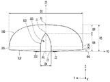
図7は、第2実施例として図1の光学レンズのA‐A側断面図であり、図8は第2実施例として、図1の光学レンズのB‐B側側断面図である。第2実施例の説明において、第1実施例と同じ部分の説明は省略することにする。図7および図8の光学レンズは、図1および図2の平面図および背面図を参照することにし、第1実施例から光学レンズの長さおよび厚さ、前記リセスの長さおよび深さを変更した構成である。
7 is a cross-sectional view taken along the AA side of the optical lens of FIG. 1 as a second embodiment, and FIG. 8 is a cross-sectional view taken along the BB side of the optical lens of FIG. 1 as a second embodiment. In the description of the second embodiment, the description of the same part as that of the first embodiment will be omitted. For the optical lenses of FIGS. 7 and 8, the plan view and the rear view of FIGS. 1 and 2 are referred to, and the length and thickness of the optical lens and the length and depth of the recess are determined from the first embodiment. It is a modified configuration.
図7および図8に示すように、第2実施例に係る光学レンズは、底面310、前記底面310の中心領域に凹状のリセス(recess)315、前記底面310および前記リセス315の反対側に配置された第1出射面330を含む。前記光学レンズは第1出射面330と底面310との間に第2出射面335を含むことができる。このような第2実施例に係る光学レンズは、第1実施例の光学レンズと異なる部分に対して説明することにする。
As shown in FIGS. 7 and 8, the optical lens according to the second embodiment is arranged on the bottom surface 310, the recessed recess 315 in the central region of the bottom surface 310, and opposite the bottom surface 310 and the recess 315. The first exit surface 330 is included. The optical lens may include a second exit surface 335 between the first exit surface 330 and the bottom surface 310. The optical lens according to the second embodiment will be described with respect to a portion different from the optical lens of the first embodiment.
前記光学レンズの底面310には、複数の支持突起350を含むことができる。前記複数の支持突起350は、前記光学レンズ300の底面310から下方に突出して前記光学レンズ300を支持することになる。このような支持突起350は第1実施例を参照することにする。
The bottom surface 310 of the optical lens may include a plurality of support protrusions 350. The plurality of support protrusions 350 project downward from the bottom surface 310 of the optical lens 300 to support the optical lens 300. Such a support protrusion 350 will be referred to in the first embodiment.
図7および図8の光学レンズは、第1、2出射面330、335を介して上方および側方に光を放出し、前記第1、2出射面330、335を介して出射された光量は光学レンズの頂点に水平な直線を基準に上方よりは下方により多くの光が放出される。これは第1実施例の光学レンズが上方により多くの光量を照射するのと違い、第2実施例の光学レンズは側方により多くの光量を照射しており、側発光レンズとして提供されることができる。
The optical lenses of FIGS. 7 and 8 emit light upward and laterally through the first and second exit surfaces 330 and 335, and the amount of light emitted through the first and second exit surfaces 330 and 335 is More light is emitted downward than above, relative to a straight line horizontal to the apex of the optical lens. This is different from the optical lens of the first embodiment irradiating a larger amount of light upward, and the optical lens of the second embodiment irradiates a larger amount of light to the side and is provided as a side emitting lens. Can be done.
前記底面310のボトムビュー形状は楕円形状を含むことができる。前記底面310または第1出射面330の長さは、X軸方向の第1長さ(D1)とY軸方向の第2長さ(D2)が異なる。前記第1長さ(D1)は光学レンズ300のX軸方向の長さであり、第2長さ(D2)はY軸方向の長さである。前記第1長さ(D1)は第2長さ(D2)より長く配置され、前記第1長さ(D1)が第2長さ(D2)より1mm以上、例えば2mm以上大きい。前記長さはD2>D1の条件を満足し、前記長さの比率(D1:D2)の比率は1:1.08〜1:1.4の範囲を有することができる。実施例に係る光学レンズ300は、第2長さ(D2)が第1長さ(D1)より長く配置されるので、Y軸方向の輝度分布が減少しないようにすることができる。
The bottom view shape of the bottom surface 310 can include an elliptical shape. The length of the bottom surface 310 or the first exit surface 330 is different from the first length (D1) in the X-axis direction and the second length (D2) in the Y-axis direction. The first length (D1) is the length of the optical lens 300 in the X-axis direction, and the second length (D2) is the length in the Y-axis direction. The first length (D1) is arranged longer than the second length (D2), and the first length (D1) is 1 mm or more, for example, 2 mm or more larger than the second length (D2). The length satisfies the condition of D2> D1, and the ratio of the length ratio (D1: D2) can have a range of 1: 1.08 to 1: 1.4. Since the optical lens 300 according to the embodiment has a second length (D2) longer than the first length (D1), it is possible to prevent the brightness distribution in the Y-axis direction from decreasing.
前記リセス315の底の形状は楕円形状を含むことができる。図8および図9のように、前記リセス315は、側断面が鐘(bell)形状、砲弾(shell)形状または楕円形状を含むことができる。前記リセス315は上方に行くほど幅が段々狭くなる形状を有することができる。前記リセス315は、底の周りの第1エッジ23から上端の第1頂点21に向かって徐々に収束される形状を有することができる。前記リセス315のボトムビューが楕円形状である場合、前記第1頂点21に向かって直径が徐々に減少することになる。前記リセス315は中心軸(Z0)を基準に軸対称形状に提供されてもよい。前記入射面320の第1頂点21はドット形状に提供されてもよい。
The shape of the bottom of the recess 315 can include an elliptical shape. As shown in FIGS. 8 and 9, the recess 315 may include a bell-shaped, shell-shaped or oval-shaped side cross section. The recess 315 can have a shape in which the width gradually narrows toward the upper side. The recess 315 can have a shape that gradually converges from the first edge 23 around the bottom to the first apex 21 at the top. When the bottom view of the recess 315 is elliptical, the diameter gradually decreases toward the first apex 21. The recess 315 may be provided in an axisymmetric shape with respect to the central axis (Z0). The first apex 21 of the incident surface 320 may be provided in a dot shape.
前記リセス315の底の長さ(D3、D4)は、光源、すなわち後述される発光素子が挿入され得る幅を有することができる。前記リセス315の底の長さ(D3、D4)は、発光素子の幅の3倍以下、例えば2.5倍以下である。前記リセス315の底の長さ(D3、D4)は、前記発光素子の幅の1.2倍〜2.5倍の範囲であり、前記範囲より小さい場合、発光素子の挿入が不容易であり、前記範囲より大きい場合、前記発光素子と第1エッジ23との間の領域を介した光損失または光干渉を起こすことがある。
The bottom length (D3, D4) of the recess 315 can have a width into which a light source, that is, a light emitting element described later can be inserted. The bottom length (D3, D4) of the recess 315 is 3 times or less, for example 2.5 times or less the width of the light emitting element. The bottom length (D3, D4) of the recess 315 is in the range of 1.2 times to 2.5 times the width of the light emitting element, and if it is smaller than the range, it is difficult to insert the light emitting element. If it is larger than the above range, light loss or light interference may occur through the region between the light emitting element and the first edge 23.
前記リセス315の底の長さは、X軸方向の長さ(D3)はY軸方向の長さ(D4)と異なってもよい。例えば、X軸方向の長さ(D3)はY軸方向の長さ(D4)より大きい。前記リセス315の底の長さはD3>D4の条件を満足し、その差は1.5mm以上5mm以下、例えば1.5mm〜5mmの差を有することができる。前記幅D3はD4の2倍以下である。前記リセス315の底の長さの比率(D4:D3)は1:1.3〜1:1.8の範囲の差を有することができる。このようなY軸方向の長さ(D4)がX軸方向の長さ(D3)より前記範囲より小さい場合、Y軸方向の輝度改善が微小で、前記範囲より大きい場合、X軸方向の輝度分布が相対的に小さくなる。また、リセス315の底の長さ(D3、D4)間の幅の差が大きくなることで、光源、例えば発光素子から放出された光が、リセスの幅が広い方向、例えばX軸方向への光抽出効率の改善を誘導することができる。
Regarding the length of the bottom of the recess 315, the length in the X-axis direction (D3) may be different from the length in the Y-axis direction (D4). For example, the length in the X-axis direction (D3) is larger than the length in the Y-axis direction (D4). The bottom length of the recess 315 satisfies the condition of D3> D4, and the difference can have a difference of 1.5 mm or more and 5 mm or less, for example, 1.5 mm to 5 mm. The width D3 is twice or less the width of D4. The bottom length ratio (D4: D3) of the recess 315 can have a difference in the range 1: 1.3 to 1: 1.8. When the length (D4) in the Y-axis direction is smaller than the length (D3) in the X-axis direction, the improvement in brightness in the Y-axis direction is small, and when it is larger than the range, the brightness in the X-axis direction is small. The distribution is relatively small. Further, the difference in width between the bottom lengths (D3, D4) of the recess 315 becomes large, so that the light emitted from the light source, for example, the light emitting element can be directed in the direction in which the recess width is wide, for example, in the X-axis direction. It is possible to induce an improvement in light extraction efficiency.
実施例に係る光学レンズ300は、底面310または第1出射面330のD2/D1の比率はaであり、前記リセス315のD3/D4の比率がbである場合、a<bの関係を有することができる。前記長さの比率D2/D1は長/短長さの比率であり、D3/D4は長/短長さの比率である。
The optical lens 300 according to the embodiment has a relationship of a <b when the ratio of D2 / D1 of the bottom surface 310 or the first exit surface 330 is a and the ratio of D3 / D4 of the recess 315 is b. be able to. The length ratio D2 / D1 is a length / short length ratio, and D3 / D4 is a length / short length ratio.
前記bはaの125%以上、例えば125%〜160%の範囲で提供される。これは非対称光学レンズにおいて、前記リセス315の入射面310が対称レンズより広く提供されるので、光をさらに広い範囲まで拡散させて提供することができる。これによって、光学レンズ300は、外形的な長さの差によってY軸方向の輝度分布を確保することができ、輝度分布の側面で前記リセス315によってX軸方向および角領域に広く拡散させることができる。これによって、前記光学レンズ300が配列された光源モジュールのバーの個数を2個以下、例えば1個に減らすことができ、バックライトユニットにおける上下コーナー部の輝度分布を改善させることができる。
The b is provided in the range of 125% or more of a, for example, 125% to 160%. This is because in an asymmetric optical lens, the incident surface 310 of the recess 315 is provided wider than that of a symmetric lens, so that light can be diffused and provided over a wider range. As a result, the optical lens 300 can secure the luminance distribution in the Y-axis direction due to the difference in external length, and can be widely diffused in the X-axis direction and the angular region by the recess 315 on the side surface of the luminance distribution. it can. As a result, the number of bars of the light source module in which the optical lens 300 is arranged can be reduced to two or less, for example, one, and the brightness distribution at the upper and lower corners of the backlight unit can be improved.
前記光学レンズ300の第2出射面335は、前記リセス315の底に水平な第1直線(X0)および第2直線(Y0)より高い位置に配置される。前記第2出射面335はフラットな面または傾斜した面からなることができ、フランジ(Flange)と定義することができるが、これに対して限定はしない。
The second exit surface 335 of the optical lens 300 is arranged at a position higher than the first straight line (X0) and the second straight line (Y0) horizontal to the bottom of the recess 315. The second exit surface 335 can consist of a flat surface or an inclined surface and can be defined as a flange, but is not limited thereto.
前記第2出射面335は、前記水平な第1直線(X0)および第2直線(Y0)に対して垂直または傾斜するように配置される。前記第2出射面335は、前記第1出射面330の外枠ラインから垂直または傾斜するように延長される。前記第2出射面335は第1出射面330に隣接した第3エッジ35を含み、前記第3エッジ35は、前記第1出射面330の外枠ラインと同一位置であるか、前記第1出射面330の外枠ラインより内部または外部に位置することができる。
The second exit surface 335 is arranged so as to be perpendicular or inclined with respect to the horizontal first straight line (X0) and the second straight line (Y0). The second exit surface 335 extends vertically or inclined from the outer frame line of the first exit surface 330. The second exit surface 335 includes a third edge 35 adjacent to the first exit surface 330, and the third edge 35 is located at the same position as the outer frame line of the first exit surface 330 or the first exit surface. It can be located inside or outside the outer frame line of the surface 330.
前記第2出射面335の第3エッジ35と前記中心軸(Z0)を連結した直線は、前記リセス315の底の中心(P0)を基準に前記中心軸(Z0)から70±2度以下の角度に位置することができる。前記第2出射面335の第3エッジ35は、前記リセス315の底の中心(P0)を基準に前記水平な第1直線(X0)および第2直線(Y0)に対して20度以下、例えば16±2度の角度で位置することができる。前記リセス315の底の中心(P0)に前記第2出射面335の第2エッジ25と第3エッジ35との間の角度は16度以下、例えば13±2度の角度を有することができる。このような第2出射面335の第3エッジ35を通る直線に対する角度は、前記光学レンズ300の外部角度である。前記第2出射面335は、前記水平な第1直線(X0)および第2直線(Y0)から離隔した領域から入射する光を屈折させて放射することができる。前記第2出射面335によって屈折された光は、中心軸(Z0)を基準に屈折前の角度より小さい角度で放射されることになる。これによって、第2出射面335は屈折された光が水平な直線より低い方向に放射されることができ、ライトユニットの反射シートによって反射される。
The straight line connecting the third edge 35 of the second exit surface 335 and the central axis (Z0) is 70 ± 2 degrees or less from the central axis (Z0) with reference to the center (P0) of the bottom of the recess 315. Can be located at an angle. The third edge 35 of the second exit surface 335 is 20 degrees or less with respect to the horizontal first straight line (X0) and second straight line (Y0) with respect to the center (P0) of the bottom of the recess 315, for example. It can be positioned at an angle of 16 ± 2 degrees. The angle between the second edge 25 and the third edge 35 of the second exit surface 335 at the center (P0) of the bottom of the recess 315 can be 16 degrees or less, for example, an angle of 13 ± 2 degrees. The angle of the second exit surface 335 with respect to the straight line passing through the third edge 35 is the external angle of the optical lens 300. The second exit surface 335 can refract and emit light incident from a region separated from the horizontal first straight line (X0) and the second straight line (Y0). The light refracted by the second exit surface 335 is emitted at an angle smaller than the angle before refraction with respect to the central axis (Z0). As a result, the refracted light can be emitted from the second exit surface 335 in a direction lower than the horizontal straight line, and is reflected by the reflection sheet of the light unit.
前記中心軸(Z0)と前記底面310の第2エッジ25を通る直線は、前記第1直線(X0)または第2軸(Y0)との角度(θ1)が5度以下、例えば0.4度〜4度の範囲を有することができる。このような角度(θ1)は、前記中心軸(Z0)との距離と前記第2エッジ25の高さによって変わり、前記範囲を外れる場合、光学レンズの厚さが変更されて光の損失が増加することがある。前記第2出射面335は、前記リセス315の底の中心(P0)を基準に前記中心軸(Z0)から半値角を外れる光を屈折させるので、光損失を減らすことができる。
The straight line passing through the central axis (Z0) and the second edge 25 of the bottom surface 310 has an angle (θ1) of 5 degrees or less, for example, 0.4 degrees between the first straight line (X0) or the second axis (Y0). It can have a range of ~ 4 degrees. Such an angle (θ1) changes depending on the distance from the central axis (Z0) and the height of the second edge 25, and when it is out of the range, the thickness of the optical lens is changed and the light loss increases. I have something to do. Since the second exit surface 335 refracts light deviating from the central axis (Z0) with reference to the center (P0) of the bottom of the recess 315, light loss can be reduced.
前記光学レンズ300の長さ(D1、D2)は、厚さ(D5)より大きく配置されてもよい。前記光学レンズ300の長さ(D1、D2)は、前記厚さ(D5)の2.5倍以上、例えば3倍以上となることができる。前記第1長さ(D1)は15mm以上、例えば16mm〜25mmの範囲を有することができ、第2長さ(D2)は17mm以上、例えば17mm〜30mmの範囲を有することができる。前記光学レンズ300の厚さ(D5)は6.5mm以上、例えば6.5mm〜9mm以下の範囲を有することができる。このような光学レンズ300の相互異なる長さ(D1、D2)が厚さ(D5)より大きく配置されるので、照明装置やライトユニットの全領域に均一な輝度分布を提供することができる。また、ライトユニット内でカバーする領域が改善されるので、光学レンズの個数を減らすことができ、光学レンズ300の厚さを減らすことができる。
The length (D1, D2) of the optical lens 300 may be arranged to be larger than the thickness (D5). The length (D1, D2) of the optical lens 300 can be 2.5 times or more, for example, 3 times or more the thickness (D5). The first length (D1) can have a range of 15 mm or more, for example 16 mm to 25 mm, and the second length (D2) can have a range of 17 mm or more, for example 17 mm to 30 mm. The thickness (D5) of the optical lens 300 can have a range of 6.5 mm or more, for example, 6.5 mm to 9 mm or less. Since the different lengths (D1, D2) of the optical lenses 300 are arranged larger than the thickness (D5), it is possible to provide a uniform luminance distribution over the entire region of the lighting device or the light unit. Further, since the area covered in the light unit is improved, the number of optical lenses can be reduced, and the thickness of the optical lens 300 can be reduced.
前記D5/D1の比率がcであり、D5/D2の比率がdである場合、前記c、dは0.3以上であり、c>dの関係を有することができる。このような光学レンズ300の長さ(D1、D2)が厚さ(D5)より大きく配置されてD2>D1、D3>D4の関係を有するので、照明装置やライトユニットの全領域に均一な輝度分布を提供することができる。また、ライトユニット内でカバーする領域が改善されるので、光学レンズの個数を減らすことができ、光学レンズ300の厚さを減らすことができる。
When the ratio of D5 / D1 is c and the ratio of D5 / D2 is d, the c and d are 0.3 or more, and the relationship of c> d can be obtained. Since the lengths (D1, D2) of such an optical lens 300 are arranged larger than the thickness (D5) and have a relationship of D2> D1 and D3> D4, uniform brightness is applied to the entire area of the lighting device or the light unit. A distribution can be provided. Further, since the area covered in the light unit is improved, the number of optical lenses can be reduced, and the thickness of the optical lens 300 can be reduced.
前記リセス315の深さ(D8)は底の中心(P0)から第1頂点21までの間隔を有する。ここで、前記第1頂点21は入射面320の頂点であるかリセス315の上端地点である。前記リセス315の深さ(D8)は4mm以上、例えば4mm〜5.2mmの範囲を有することができ、前記光学レンズ300の厚さ(D5)の0.6以上、例えば0.6〜0.7の範囲を有することができる。前記リセス315の深さ(D8)は、前記第1出射面330の第2頂点31と底の中心(P0)または第1エッジ23との間の距離の60%以上である。前記リセス315は、D3/D8の比率がeであり、D4/D8の比率がfである場合、e>fの関係を有することができる。前記リセス315の深さ(D8)が深く配置されることで、第1出射面330のセンター領域が全反射面または負の曲率を持たなくても、入射面320の第1頂点21の隣接領域においても側方に光を拡散させることができる。前記リセス315が深い深さ(D8)を有するので、前記入射面320は第2頂点31に近い領域から前記第1頂点21の周辺領域に入射した光を側方に屈折させることができる。
The depth (D8) of the recess 315 has an interval from the center of the bottom (P0) to the first apex 21. Here, the first apex 21 is the apex of the incident surface 320 or the upper end point of the recess 315. The depth (D8) of the recess 315 can have a range of 4 mm or more, for example 4 mm to 5.2 mm, and the thickness (D5) of the optical lens 300 is 0.6 or more, for example 0.6 to 0. It can have a range of 7. The depth (D8) of the recess 315 is 60% or more of the distance between the second apex 31 of the first exit surface 330 and the center (P0) of the bottom or the first edge 23. The recess 315 can have a relationship of e> f when the ratio of D3 / D8 is e and the ratio of D4 / D8 is f. By arranging the depth (D8) of the recess 315 deeply, even if the center region of the first exit surface 330 does not have a total reflection surface or a negative curvature, the region adjacent to the first vertex 21 of the incident surface 320 It is also possible to diffuse the light to the side. Since the recess 315 has a deep depth (D8), the incident surface 320 can refract light incident on the peripheral region of the first apex 21 from a region close to the second apex 31 laterally.
前記リセス315と前記第1出射面330との間の最小距離(D9)は、前記入射面320の第1頂点21と第1出射面330の第2頂点31との間の間隔である。前記距離(D9)は3mm以下、例えば2mm〜3mmの範囲を有することができる。前記入射面320の第1頂点21と第1出射面330第2頂点31との間の距離(D9)が3mmを超える場合、前記第1出射面330のセンター領域とサイド領域に進行する光量の差が大きくなり、光分布が不均一になる。前記入射面320の第1頂点21と第1出射面330の第2頂点31との間の距離(D9)が2mm未満の場合、光学レンズ300のセンター側剛性が弱くなる問題がある。このようなリセス315および第1出射面330との間の距離(D9)を前記範囲で配置することで、第2出射面335のセンター領域が全反射面または負の曲率を持たなくても、光の経路を外側方向に拡散させることができる。これは入射面320の第1頂点21が前記第1出射面330の凸状の第2頂点31に隣接するほど、前記入射面320を介して第1出射面330の側方に進行する光の光量が増加する。したがって、光学レンズ300の側方向、例えばY軸方向に拡散する光量を増加させることができる。
The minimum distance (D9) between the recess 315 and the first exit surface 330 is the distance between the first apex 21 of the entrance surface 320 and the second apex 31 of the first exit surface 330. The distance (D9) can have a range of 3 mm or less, for example 2 mm to 3 mm. When the distance (D9) between the first apex 21 of the incident surface 320 and the second apex 31 of the first exit surface 330 exceeds 3 mm, the amount of light traveling to the center region and the side region of the first exit surface 330 The difference becomes large and the light distribution becomes uneven. When the distance (D9) between the first apex 21 of the incident surface 320 and the second apex 31 of the first exit surface 330 is less than 2 mm, there is a problem that the center-side rigidity of the optical lens 300 is weakened. By arranging the distance (D9) between the recess 315 and the first exit surface 330 within the above range, even if the center region of the second exit surface 335 does not have a total reflection surface or a negative curvature, The path of light can be diffused outward. This is because the more the first apex 21 of the incident surface 320 is adjacent to the convex second apex 31 of the first exit surface 330, the light traveling laterally to the first exit surface 330 via the incident surface 320. The amount of light increases. Therefore, the amount of light diffused in the lateral direction of the optical lens 300, for example, in the Y-axis direction can be increased.
前記入射面320の第1頂点21は、前記第2出射面335の第3エッジ35から水平に延長した直線よりは第1出射面330のセンターである第2頂点31により隣接するように配置される。
The first apex 21 of the incident surface 320 is arranged so as to be adjacent to the second apex 31, which is the center of the first exit surface 330, rather than a straight line extending horizontally from the third edge 35 of the second exit surface 335. To.
前記第2出射面335の幅(D7)は第2エッジ25および第3エッジ35との間の直線距離として、前記リセス315の深さ(D8>D7)より小さくなる。前記第2出射面335の幅(D7)は、例えば1.5mm〜2.3mmの範囲を有することができる。前記第2出射面335の幅(D7)が前記範囲を超える場合、第2出射面335に出射される光量が増加して光分布制御が難しい問題があり、前記範囲より小さい場合、レンズ本体を製造する時、ゲート(Gate)領域の確保が難しくなる。
The width (D7) of the second exit surface 335 is smaller than the depth (D8> D7) of the recess 315 as a linear distance between the second edge 25 and the third edge 35. The width (D7) of the second exit surface 335 can have a range of, for example, 1.5 mm to 2.3 mm. When the width (D7) of the second exit surface 335 exceeds the above range, there is a problem that the amount of light emitted to the second exit surface 335 increases and it is difficult to control the light distribution. When manufacturing, it becomes difficult to secure a gate area.
前記光学レンズ300において、第2出射面335は第1出射面330の下部周りに配置され、底面310は前記第2出射面335の第2エッジ25より下に配置される。前記底面310は、前記第2出射面335の第2エッジ25の水平線上よりも下に突出する。前記光学レンズ300は、他の例として、前記第2出射面335に凹凸面を備えることができる。前記凹凸面は、表面が粗いヘイズ(Haze)面からなることができる。前記凹凸面は、散乱粒子が形成された面であってもよい。前記光学レンズ300は、他の例として、前記底面310に凹凸面を備えることができる。前記底面310の凹凸面は、表面が粗いヘイズ面からなるか、散乱粒子が形成されてもよい。
In the optical lens 300, the second exit surface 335 is arranged around the lower part of the first exit surface 330, and the bottom surface 310 is arranged below the second edge 25 of the second exit surface 335. The bottom surface 310 projects below the horizontal line of the second edge 25 of the second exit surface 335. As another example, the optical lens 300 may have an uneven surface on the second exit surface 335. The uneven surface can consist of a Haze surface having a rough surface. The uneven surface may be a surface on which scattered particles are formed. As another example, the optical lens 300 may have an uneven surface on the bottom surface 310. The uneven surface of the bottom surface 310 may be a haze surface having a rough surface or scattered particles may be formed.
実施例に係る光学レンズは、図13のように、回路基板400の上でY軸方向に所定間隔で配列される。このような光学レンズは長さ(D2>D1)およびリセス315の長さ(D4<D3)が広いY軸方向に配列されるので、光学レンズ300間の間隔は広くしながら光学レンズ300の個数を減らすことができ、前記リセス315の非対称構造によってX軸方向における輝度分布を改善させることができる。
As shown in FIG. 13, the optical lenses according to the embodiment are arranged on the circuit board 400 at predetermined intervals in the Y-axis direction. Since such optical lenses are arranged in the wide Y-axis direction in terms of length (D2> D1) and recess 315 (D4 <D3), the number of optical lenses 300 is widened while the distance between the optical lenses 300 is wide. The asymmetric structure of the recess 315 can improve the brightness distribution in the X-axis direction.
このような光学レンズは、図46および図47のように、Y軸方向の指向角分布がX軸方向の指向角分布より大きい。例えばY軸方向の指向角分布がX軸方向の指向角分布より10度以上、例えば10度〜25度の範囲で大きい。また、Y軸方向の指向角分布の半値幅(FWHM)は10度以上であり、中心強度は4%以上である。
In such an optical lens, as shown in FIGS. 46 and 47, the directivity angle distribution in the Y-axis direction is larger than the directivity angle distribution in the X-axis direction. For example, the directivity angle distribution in the Y-axis direction is 10 degrees or more, for example, 10 degrees to 25 degrees larger than the directivity angle distribution in the X-axis direction. The full width at half maximum (FWHM) of the directivity angle distribution in the Y-axis direction is 10 degrees or more, and the central intensity is 4% or more.
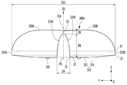
図9は第3実施例に係る光学レンズのY軸方向の側断面図であり、図10は図9の光学レンズの他のX軸方向の断面図である。
FIG. 9 is a side sectional view of the optical lens according to the third embodiment in the Y-axis direction, and FIG. 10 is a sectional view of the optical lens of FIG. 9 in the other X-axis direction.
図9および図10に示すように、第3実施例に係る光学レンズは、底面310、前記底面310のセンター領域に前記底面310から上方に膨らんだリセス(recess)315、前記底面310および前記リセス315の反対側に配置された第1出射面330、前記第1出射面330の下部に配置された第2出射面335を含む。このような第3実施例に係る光学レンズは、第1実施例の光学レンズに比べて、第1、2長さ(D1、D2)と、リセス315の長さ(D3、D4)と、リセス315の深さを異なるようにした構造である。また、第3実施例に係る光学レンズは、第2出射面335の幅(B1、B2)が領域に応じて異なる構造で提供されてもよい。
As shown in FIGS. 9 and 10, the optical lens according to the third embodiment has a bottom surface 310, a recess 315 bulging upward from the bottom surface 310 in the center region of the bottom surface 310, the bottom surface 310, and the recess. Includes a first exit surface 330 located on the opposite side of the 315 and a second exit surface 335 located below the first exit surface 330. The optical lens according to the third embodiment has a first and second length (D1, D2), a recess 315 length (D3, D4), and a recess, as compared with the optical lens of the first embodiment. It is a structure in which the depth of 315 is different. Further, the optical lens according to the third embodiment may be provided with a structure in which the widths (B1, B2) of the second exit surface 335 differ depending on the region.
前記光学レンズの底面310のボトムビュー形状は楕円形状を含むことができる。前記底面310または第1出射面330の長さは、X軸方向の第1長さ(D1)とY軸方向の第2長さ(D2)が異なる。前記第1長さ(D1)は光学レンズ300のX軸方向の長さであり、第2長さ(D2)はY軸方向の長さである。前記第1長さ(D1)は第2長さ(D2)より短く配置され、前記第1長さ(D1)が第2長さ(D2)より0.5mm以上、例えば0.5mm以上3mm以下の差を有することができる。前記長さはD2>D1の条件を満足し、前記長さの比率(D1:D2)の比率は1:1.06〜1:1.1の範囲を有することができる。実施例に係る光学レンズ300は、第1長さ(D1)が第2長さ(D2)より短く配置されるので、X軸方向の輝度分布が減少しないようにすることができる。
The bottom view shape of the bottom surface 310 of the optical lens can include an elliptical shape. The length of the bottom surface 310 or the first exit surface 330 is different from the first length (D1) in the X-axis direction and the second length (D2) in the Y-axis direction. The first length (D1) is the length of the optical lens 300 in the X-axis direction, and the second length (D2) is the length in the Y-axis direction. The first length (D1) is arranged shorter than the second length (D2), and the first length (D1) is 0.5 mm or more, for example, 0.5 mm or more and 3 mm or less than the second length (D2). Can have a difference of. The length satisfies the condition of D2> D1, and the ratio of the length ratio (D1: D2) can have a range of 1: 1.06 to 1: 1.1. Since the optical lens 300 according to the embodiment has a first length (D1) shorter than the second length (D2), the brightness distribution in the X-axis direction can be prevented from decreasing.
前記リセス315の底の形状は楕円形状を含むことができる。前記リセス315は、側断面が鐘(bell)形状、砲弾(shell)形状または楕円形状を含むことができる。前記リセス315は上方に行くほど幅が段々狭くなる形状を有することができる。前記リセス315は、底の周りの第1エッジ23から上端の第1頂点21に向かって徐々に収束される形状を有することができる。前記リセス315のボトムビューが楕円形状である場合、前記第1頂点21に向かって直径が徐々に減少することになる。前記リセス315は中心軸(Z0)を基準に軸対称形状に提供されてもよい。前記入射面320の第1頂点21はドット形状に提供されてもよい。
The shape of the bottom of the recess 315 can include an elliptical shape. The recess 315 may include a bell-shaped, shell-shaped or oval-shaped side cross section. The recess 315 can have a shape in which the width gradually narrows toward the upper side. The recess 315 can have a shape that gradually converges from the first edge 23 around the bottom to the first apex 21 at the top. When the bottom view of the recess 315 is elliptical, the diameter gradually decreases toward the first apex 21. The recess 315 may be provided in an axisymmetric shape with respect to the central axis (Z0). The first apex 21 of the incident surface 320 may be provided in a dot shape.
前記リセス315の底の長さ(D3、D4)は、光源、すなわち後述される発光素子が挿入され得る幅を有することができる。前記リセス315の底の長さ(D3、D4)は、発光素子の幅の3倍以下、例えば2.5倍以下である。前記リセス315の底の長さ(D3、D4)は、前記発光素子の幅の1.2倍〜2.5倍の範囲であり、前記範囲より小さい場合、発光素子の挿入が不容易であり、前記範囲より大きい場合、前記発光素子と第1エッジ23との間の領域を介した光損失または光干渉を起こすことがある。
The bottom length (D3, D4) of the recess 315 can have a width into which a light source, that is, a light emitting element described later can be inserted. The bottom length (D3, D4) of the recess 315 is 3 times or less, for example 2.5 times or less the width of the light emitting element. The bottom length (D3, D4) of the recess 315 is in the range of 1.2 times to 2.5 times the width of the light emitting element, and if it is smaller than the range, it is difficult to insert the light emitting element. If it is larger than the above range, light loss or light interference may occur through the region between the light emitting element and the first edge 23.
前記リセス315の底の長さは、X軸方向の長さ(D3)はY軸方向の長さ(D4)と異なってもよい。例えば、X軸方向の長さ(D3)は第2軸方向の長さ(D4)より大きい。前記リセス315の底の長さはD3>D4の関係を有し、その差は1.5mm以上5mm以下、例えば1.5mm以上3mm以下の差を有することができる。前記幅D3はD4の3倍以下、例えば2倍以下である。前記リセス315の底の長さの比率(D4:D3)は1:1.5〜1:3の範囲の差を有することができる。このようなX軸方向のリセス315の底の長さ(D3)がY軸方向の長さ(D4)より大きく配置されるので、非対称レンズ形状に提供されることになる。
Regarding the length of the bottom of the recess 315, the length in the X-axis direction (D3) may be different from the length in the Y-axis direction (D4). For example, the length in the X-axis direction (D3) is larger than the length in the second axis direction (D4). The bottom length of the recess 315 has a relationship of D3> D4, and the difference can have a difference of 1.5 mm or more and 5 mm or less, for example, 1.5 mm or more and 3 mm or less. The width D3 is three times or less, for example, twice or less the width of D4. The bottom length ratio (D4: D3) of the recess 315 can have a difference in the range 1: 1.5 to 1: 3. Since the bottom length (D3) of the recess 315 in the X-axis direction is arranged to be larger than the length (D4) in the Y-axis direction, the recess 315 is provided in an asymmetric lens shape.
また、リセス315の底の長さ(D3、D4)間の幅の差が大きくなくても光源、例えば発光素子から放出された光が、リセスの幅が広い方向、例えばY軸方向への光抽出効率の改善を誘導することができる。
Further, even if the difference in width between the bottom lengths (D3, D4) of the recess 315 is not large, the light emitted from the light source, for example, the light emitting element is the light in the direction in which the width of the recess is wide, for example, the Y-axis direction. It is possible to induce an improvement in extraction efficiency.
実施例に係る光学レンズは、外形的にX軸方向の第1長さ(D1)がY軸方向の第2長さ(D2)より短く、前記リセス315が底の長さはX軸方向の長さ(D3)がY軸方向の長さ(D4)より広く配置されることになる。これによって、光学レンズ300は、外形的な長さの差によってY軸方向の輝度分布を確保することができ、輝度分布の側面で前記リセス315によってX軸方向および角領域に広く拡散させることができる。
In the optical lens according to the embodiment, the first length (D1) in the X-axis direction is shorter than the second length (D2) in the Y-axis direction, and the recess 315 has a bottom length in the X-axis direction. The length (D3) is arranged wider than the length (D4) in the Y-axis direction. As a result, the optical lens 300 can secure the luminance distribution in the Y-axis direction due to the difference in external length, and can be widely diffused in the X-axis direction and the angular region by the recess 315 on the side surface of the luminance distribution. it can.
実施例に係る光学レンズは、底面310または第1出射面330の長さD2/D1の比率はaであり、前記リセス315の長さD3/D4の比率がbである場合、a<bの関係を有することができる。前記長さD2/D1は底面310または第1出射面330において長さの長/短比率であり、D3/D4はリセス315の底において長さの長/短比率である。前記bはaの120%以上、例えば120%〜145%または130%〜280%の範囲で提供される。前記bはaの1.2倍以上、例えば1.2倍〜1.45倍や1.3倍〜2.8倍の範囲で提供される。これは非対称光学レンズにおいて、前記リセス315の入射面320が対称レンズより広く提供されるので、光をさらに広い範囲まで拡散させて提供することができる。これによって、光学レンズ300は、外形的な長さの差によってY軸方向の輝度分布を確保することができ、輝度分布の側面で前記リセス315によってX軸方向および放射方向に広く拡散させることができる。これによって、前記光学レンズ300が配列された光源モジュールのバーの個数を2個以下、例えば1個に減らすことができ、バックライトユニットにおける上下コーナー部の輝度分布を改善させることができる。
In the optical lens according to the embodiment, when the ratio of the length D2 / D1 of the bottom surface 310 or the first exit surface 330 is a and the ratio of the length D3 / D4 of the recess 315 is b, a <b. Can have a relationship. The length D2 / D1 is the length / short ratio at the bottom surface 310 or the first exit surface 330, and D3 / D4 is the length / short ratio at the bottom of the recess 315. The b is provided in the range of 120% or more of a, for example 120% to 145% or 130% to 280%. The b is provided in the range of 1.2 times or more of a, for example, 1.2 times to 1.45 times or 1.3 times to 2.8 times. This is because in the asymmetric optical lens, the incident surface 320 of the recess 315 is provided wider than that of the symmetric lens, so that the light can be diffused and provided in a wider range. As a result, the optical lens 300 can secure the luminance distribution in the Y-axis direction due to the difference in external length, and can be widely diffused in the X-axis direction and the radial direction by the recess 315 on the side surface of the luminance distribution. it can. As a result, the number of bars of the light source module in which the optical lens 300 is arranged can be reduced to two or less, for example, one, and the brightness distribution at the upper and lower corners of the backlight unit can be improved.
前記光学レンズ300の第2出射面335は、前記リセス315の底に水平な第1直線(X0)および第2直線(Y0)より高い位置に配置される。前記第2出射面335はフラットな面または傾斜した面からなることができ、フランジ(Flange)と定義することができるが、これに対して限定はしない。
The second exit surface 335 of the optical lens 300 is arranged at a position higher than the first straight line (X0) and the second straight line (Y0) horizontal to the bottom of the recess 315. The second exit surface 335 can consist of a flat surface or an inclined surface and can be defined as a flange, but is not limited thereto.
前記第2出射面335は、前記水平な第1直線(X0)および第2直線(Y0)に対して垂直または傾斜するように配置される。前記第2出射面335は、前記第1出射面330の外枠ラインから垂直または傾斜するように延長される。前記第2出射面335は第1出射面330に隣接した第3エッジ35を含み、前記第3エッジ35は、前記第1出射面330の外枠ラインと同一位置であるか、前記第1出射面330の外枠ラインより内部または外部に位置することができる。
The second exit surface 335 is arranged so as to be perpendicular or inclined with respect to the horizontal first straight line (X0) and the second straight line (Y0). The second exit surface 335 extends vertically or inclined from the outer frame line of the first exit surface 330. The second exit surface 335 includes a third edge 35 adjacent to the first exit surface 330, and the third edge 35 is located at the same position as the outer frame line of the first exit surface 330 or the first exit surface. It can be located inside or outside the outer frame line of the surface 330.
前記第2出射面335の第3エッジ35と前記中心軸(Z0)を連結した直線は、前記リセス315の底の中心(P0)を基準に前記中心軸(Z0)から74±2度以下の角度に位置することができる。前記第2出射面335の第3エッジ35は、前記リセス315の底の中心(P0)を基準に前記水平な第1直線(X0)および第2軸(Y0)に対して20度以下、例えば16±2度の角度で位置することができる。前記リセス315の底の中心(P0)に前記第2出射面335の第2エッジ25と第3エッジ35との間の角度は16度以下、例えば13±2度の角度を有することができる。このような第2出射面335の第3エッジ35を通る直線に対する角度は、前記光学レンズ300の外部角度である。前記第2出射面335は、前記水平な第1直線(X0)および第2軸(Y0)から離隔した領域から入射する光を屈折させて放射することができる。前記第2出射面335によって屈折された光は、中心軸(Z0)を基準に屈折前の角度より小さい角度で放射されることになる。これによって、第2出射面335は屈折された光が水平な軸または水平な軸より低い方向に放射されることを抑制することができ、隣接した光学部材に干渉を与えたり光が損失することを防止することができる。
The straight line connecting the third edge 35 of the second exit surface 335 and the central axis (Z0) is 74 ± 2 degrees or less from the central axis (Z0) with reference to the center (P0) of the bottom of the recess 315. Can be located at an angle. The third edge 35 of the second exit surface 335 is 20 degrees or less with respect to the horizontal first straight line (X0) and the second axis (Y0) with respect to the center (P0) of the bottom of the recess 315, for example. It can be positioned at an angle of 16 ± 2 degrees. The angle between the second edge 25 and the third edge 35 of the second exit surface 335 at the center (P0) of the bottom of the recess 315 can be 16 degrees or less, for example, an angle of 13 ± 2 degrees. The angle of the second exit surface 335 with respect to the straight line passing through the third edge 35 is the external angle of the optical lens 300. The second exit surface 335 can refract and emit light incident from a region separated from the horizontal first straight line (X0) and the second axis (Y0). The light refracted by the second exit surface 335 is emitted at an angle smaller than the angle before refraction with respect to the central axis (Z0). As a result, the second exit surface 335 can suppress the refracted light from being emitted in a direction lower than the horizontal axis or the horizontal axis, which causes interference to the adjacent optical member or loss of light. Can be prevented.
前記中心軸(Z0)と前記底面310の第2エッジ25を通る直線は、前記第1直線(X0)または第2軸(Y0)との角度(θ1、θ2)が5度以下、例えば0.4度〜4度の範囲を有することができる。前記第1直線(X0)または第2直線(Y0)との角度(θ1、θ2)は、相互同一であるか1度以下の差を有することができる。このような角度(θ1、θ2)は、前記中心軸(Z0)との距離と前記第2エッジ25の高さによって変わり、前記範囲を外れる場合、光学レンズの厚さが変更されて光の損失が増加することがある。前記第2出射面335は、前記リセス315の底の中心(P0)を基準に前記中心軸(Z0)から半値角を外れる光を屈折させるので、光損失を減らすことができる。
The straight line passing through the central axis (Z0) and the second edge 25 of the bottom surface 310 has an angle (θ1, θ2) between the first straight line (X0) or the second axis (Y0) of 5 degrees or less, for example, 0. It can have a range of 4 to 4 degrees. The angles (θ1, θ2) with the first straight line (X0) or the second straight line (Y0) can be the same or have a difference of 1 degree or less. Such angles (θ1, θ2) vary depending on the distance from the central axis (Z0) and the height of the second edge 25, and when the angle is out of the range, the thickness of the optical lens is changed and light loss occurs. May increase. Since the second exit surface 335 refracts light deviating from the central axis (Z0) with reference to the center (P0) of the bottom of the recess 315, light loss can be reduced.
前記光学レンズ300の長さ(D1、D2)は、厚さ(D5)より大きく配置されてもよい。前記光学レンズ300の長さ(D1、D2)は、前記厚さ(D5)の2.5倍以上、例えば3倍以上となることができる。前記光学レンズ300の長さのうち第1長さ(D1)は15mm以上、例えば16mm〜26mmの範囲を有することができ、第2長さ(D2)は17mm以上、例えば17mm〜30mmの範囲を有することができる。前記光学レンズ300の厚さ(D5)は6.5mm以上、例えば6.5mm〜9mm以下の範囲を有することができる。このような光学レンズ300の相互異なる長さ(D1、D2)が厚さ(D5)より大きく配置されるので、照明装置やライトユニットの全領域に均一な輝度分布を提供することができる。また、ライトユニット内でカバーする領域が改善されるので、光学レンズの個数を減らすことができ、光学レンズ300の厚さを減らすことができる。
The length (D1, D2) of the optical lens 300 may be arranged to be larger than the thickness (D5). The length (D1, D2) of the optical lens 300 can be 2.5 times or more, for example, 3 times or more the thickness (D5). Of the lengths of the optical lens 300, the first length (D1) can have a range of 15 mm or more, for example, 16 mm to 26 mm, and the second length (D2) can have a range of 17 mm or more, for example, 17 mm to 30 mm. Can have. The thickness (D5) of the optical lens 300 can have a range of 6.5 mm or more, for example, 6.5 mm to 9 mm or less. Since the different lengths (D1, D2) of the optical lenses 300 are arranged larger than the thickness (D5), it is possible to provide a uniform luminance distribution over the entire region of the lighting device or the light unit. Further, since the area covered in the light unit is improved, the number of optical lenses can be reduced, and the thickness of the optical lens 300 can be reduced.
前記リセス315の深さ(D8)は底の中心(P0)から第1頂点21までの間隔を有する。ここで、前記第1頂点21は入射面320の頂点であるかリセス315の上端地点である。前記リセス315の深さ(D8)は3mm以上、例えば4mm以上有することができ、前記光学レンズ300の厚さ(D5)の60%以上、例えば63%以上の深さを有することができる。前記リセス315の深さ(D8)が第1実施例に比べて深くなくても、第1出射面330のセンター領域が全反射面または負の曲率を持たなくなった場合、入射面320の第1頂点21の隣接領域においても側方に光を拡散させることができる。前記リセス315が低い深さ(D8)を有し、リセス315の幅の差によってY軸方向への光抽出効率を改善させることができる。
The depth (D8) of the recess 315 has an interval from the center of the bottom (P0) to the first apex 21. Here, the first apex 21 is the apex of the incident surface 320 or the upper end point of the recess 315. The recess 315 can have a depth (D8) of 3 mm or more, for example 4 mm or more, and can have a depth of 60% or more, for example 63% or more of the thickness (D5) of the optical lens 300. Even if the depth (D8) of the recess 315 is not deeper than that of the first embodiment, when the center region of the first exit surface 330 no longer has a total reflection surface or a negative curvature, the first of the incident surface 320. Light can be diffused laterally even in the region adjacent to the apex 21. The recess 315 has a low depth (D8), and the difference in width of the recess 315 can improve the light extraction efficiency in the Y-axis direction.
前記リセス315と前記第1出射面330との間の最小距離(D9)は、前記入射面320の第1頂点21と第1出射面330の第2頂点31との間の間隔である。前記距離(D9)は5mm未満、例えば1mm〜3.5mmの範囲を有することができる。前記入射面320の第1頂点21と第1出射面330第2頂点31との間の距離(D9)が5mm以上である場合、リセス315の低い深さによって光抽出効率が低下することがある。上記した構造を有するリセス315によって、前記第1出射面330のX軸方向に比べてY軸方向への光拡散を効果的に行うことができる。
The minimum distance (D9) between the recess 315 and the first exit surface 330 is the distance between the first apex 21 of the entrance surface 320 and the second apex 31 of the first exit surface 330. The distance (D9) can be less than 5 mm, for example in the range of 1 mm to 3.5 mm. When the distance (D9) between the first apex 21 of the incident surface 320 and the second apex 31 of the first exit surface 330 is 5 mm or more, the light extraction efficiency may decrease due to the low depth of the recess 315. .. The recess 315 having the above-mentioned structure can effectively diffuse light in the Y-axis direction as compared with the X-axis direction of the first exit surface 330.
前記入射面320の第1頂点21は、前記第2出射面335の第3エッジ35から水平に延長した直線よりは第1出射面330のセンターである第2頂点31により隣接するように配置される。
The first apex 21 of the incident surface 320 is arranged so as to be adjacent to the second apex 31, which is the center of the first exit surface 330, rather than a straight line extending horizontally from the third edge 35 of the second exit surface 335. To.
前記第2出射面335の幅(B1、B2)は、第2エッジ25および第3エッジ35との間の直線距離である。前記第2出射面335の幅(B1、B2)は、水平な第1直線(X0)方向の第2エッジ25に近い領域の幅(B2)が最も広く、第2直線(Y0)方向の第2エッジ25に近い領域の幅(B1)が最も狭い。また前記水平な第1直線(X0)方向の第2エッジ25に近いほど幅(B2)が段々広くなり、第2直線(Y0)方向の第2エッジ25に近いほど幅(B1)が段々狭くなる。前記第2出射面335の幅はB2>B1の関係を有することができ、B2はB1より0.1mm以上大きい。
The width (B1, B2) of the second exit surface 335 is a linear distance between the second edge 25 and the third edge 35. The width (B1, B2) of the second exit surface 335 has the widest width (B2) in the region close to the second edge 25 in the horizontal first straight line (X0) direction, and is the second in the second straight line (Y0) direction. The width (B1) of the region close to the two edges 25 is the narrowest. Further, the width (B2) becomes wider as it gets closer to the second edge 25 in the horizontal first straight line (X0) direction, and the width (B1) becomes narrower as it gets closer to the second edge 25 in the second straight line (Y0) direction. Become. The width of the second exit surface 335 can have a relationship of B2> B1, and B2 is 0.1 mm or more larger than B1.
前記第2出射面335の幅(B1、B2)のうち最大幅(B2)は、前記リセス315の深さ(D8)より小さくなる。前記第2出射面335の幅(B1、B2)は、例えば1.5mm〜2.3mmの範囲を有することができる。前記第2出射面335の幅(B2)が前記範囲を超える場合、第2出射面335に出射される光量が増加して光分布制御が難しい問題がある。ここで、第2出射面335は幅(B2)を有する領域がレンズ本体を製造する時、ゲート(Gate)領域として使用される。
The maximum width (B2) of the widths (B1, B2) of the second exit surface 335 is smaller than the depth (D8) of the recess 315. The width (B1, B2) of the second exit surface 335 can have a range of, for example, 1.5 mm to 2.3 mm. When the width (B2) of the second exit surface 335 exceeds the above range, there is a problem that the amount of light emitted to the second exit surface 335 increases and it is difficult to control the light distribution. Here, the second exit surface 335 is used as a gate region when the region having the width (B2) manufactures the lens body.
前記光学レンズ300において、第2出射面335は第1出射面330の下部周りに配置され、底面310は前記第2出射面335の第2エッジ25より下に配置される。前記底面310は、前記第2出射面335の第2エッジ25の水平線上よりも下に突出する。前記光学レンズ300は、他の例として、前記第2出射面335に凹凸面を備えることができる。前記凹凸面は、表面が粗いヘイズ(Haze)面からなることができる。前記凹凸面は、散乱粒子が形成された面であってもよい。前記光学レンズ300は、他の例として、前記底面310に凹凸面を備えることができる。前記底面310の凹凸面は、表面が粗いヘイズ面からなるか、散乱粒子が形成されてもよい。
In the optical lens 300, the second exit surface 335 is arranged around the lower part of the first exit surface 330, and the bottom surface 310 is arranged below the second edge 25 of the second exit surface 335. The bottom surface 310 projects below the horizontal line of the second edge 25 of the second exit surface 335. As another example, the optical lens 300 may have an uneven surface on the second exit surface 335. The uneven surface can consist of a Haze surface having a rough surface. The uneven surface may be a surface on which scattered particles are formed. As another example, the optical lens 300 may have an uneven surface on the bottom surface 310. The uneven surface of the bottom surface 310 may be a haze surface having a rough surface or scattered particles may be formed.
実施例に係る光学レンズは、図13のように、回路基板400の上でX軸方向に所定間隔で配列される。このような光学レンズは、リセス315の長さD4<D3の関係によってX軸方向の入射面の長さを長くすることができ、光学レンズ300間の間隔は広くしながら光学レンズ300の個数を減らすことができ、前記リセス315の非対称構造によってY軸方向における輝度分布を改善させることができる。前記回路基板400は、X軸方向に長い長さを有することができる。
As shown in FIG. 13, the optical lenses according to the embodiment are arranged on the circuit board 400 at predetermined intervals in the X-axis direction. In such an optical lens, the length of the incident surface in the X-axis direction can be increased by the relationship of the recesses 315 length D4 <D3, and the number of optical lenses 300 can be increased while widening the interval between the optical lenses 300. It can be reduced, and the asymmetric structure of the recess 315 can improve the brightness distribution in the Y-axis direction. The circuit board 400 can have a long length in the X-axis direction.
図11および図12は第4実施例に係る光学レンズとして、第2実施例の変形例として、第1軸および第2軸方向の断面図である。第4実施例の説明において、上記に開示された実施例と同じ部分は、前記実施例の説明を参照することにする。
11 and 12 are cross-sectional views taken along the first axis and the second axis as an optical lens according to a fourth embodiment and as a modified example of the second embodiment. In the description of the fourth embodiment, the same parts as those of the example disclosed above will be referred to the description of the embodiment.
図11および図12に示すように、光学レンズ300は、底面310、前記底面310のセンター領域に前記底面310から上方に膨らんだリセス(recess)315、前記リセス315の周りに入射面320、前記底面310および前記リセス315の反対側に配置された第1出射面330、前記第1出射面330の下部に配置された第2出射面335を含む。
As shown in FIGS. 11 and 12, the optical lens 300 has a bottom surface 310, a recess 315 bulging upward from the bottom surface 310 in the center region of the bottom surface 310, an incident surface 320 around the recess 315, said. It includes a first exit surface 330 arranged on the opposite side of the bottom surface 310 and the recess 315, and a second exit surface 335 arranged below the first exit surface 330.
前記光学レンズは第1出射面330の中心領域に凹状の凹部330Aを有することができ、前記凹部330Aは中心に行くほど深い深さを有することができる。このような凹部330Aは、入射する光を側方向に反射させる全反射面として提供される。前記凹部330Aは、リセス315の頂点21と対応する地点が最も低い地点31Bであり、凹状の曲面または相互異なる曲率を有する曲面を含むことができる。
The optical lens can have a concave recess 330A in the central region of the first exit surface 330, and the recess 330A can have a deeper depth toward the center. Such a recess 330A is provided as a total reflection surface that reflects incident light laterally. The recess 330A is the lowest point 31B corresponding to the apex 21 of the recess 315 and may include a concave curved surface or a curved surface having different curvatures.
図11および図12に開示された光学レンズにおいて、第1軸方向の長さ(D1)、第2軸方向の長さ(D2)、厚さ(D5)、リセス315の第1、2軸方向の長さ(D3、D4)、リセス315の深さ(D8)、前記リセス315と地点31Bの間の距離(D9)は、上記に開示された実施例から選択することができる。前記長さの比率D2/D1およびD3/D4は、上記に開示された値から選択することができ、D2/D1<D3/D4の関係を有することができる。
In the optical lenses disclosed in FIGS. 11 and 12, the length in the first axial direction (D1), the length in the second axial direction (D2), the thickness (D5), and the first and second axial directions of the recess 315. The length (D3, D4), the depth of the recess 315 (D8), and the distance between the recess 315 and the point 31B (D9) can be selected from the examples disclosed above. The length ratios D2 / D1 and D3 / D4 can be selected from the values disclosed above and can have a relationship of D2 / D1 <D3 / D4.
図13は実施例に係る光学レンズを有する光源モジュールを示した図であり、図14は図13の光源モジュールのG‐G側断面図であり、図15は図14の光源モジュールのH‐H側断面図である。
13 is a view showing a light source module having an optical lens according to an embodiment, FIG. 14 is a cross-sectional view of the light source module of FIG. 13 on the GG side, and FIG. 15 is an HH of the light source module of FIG. It is a side sectional view.
図13〜図15に示すように、光源モジュール400Aは回路基板400の上に複数の光学レンズ300が配置され、前記光学レンズ300内には少なくとも1つの発光素子100が配置される。
As shown in FIGS. 13 to 15, in the light source module 400A, a plurality of optical lenses 300 are arranged on the circuit board 400, and at least one light emitting element 100 is arranged in the optical lens 300.
前記発光素子100は、1つまたは複数個が前記回路基板400の上に所定間隔で配列される。前記発光素子100は、前記光学レンズ300と前記回路基板400との間に配置され、前記回路基板400から電源が供給されて駆動し、光を放出することになる。
One or more of the light emitting elements 100 are arranged on the circuit board 400 at predetermined intervals. The light emitting element 100 is arranged between the optical lens 300 and the circuit board 400, and power is supplied from the circuit board 400 to drive the light emitting element 100 and emit light.
前記回路基板400は、前記発光素子100と電気的に連結される回路層を含むことができる。前記回路基板400は、樹脂材質のPCB、金属コアを有するPCB(MCPCB:Metal Core PCB)、フレキシブルPCB(FPCB:Flexible PCB)のうち少なくとも1つを含むことができるが、これに対して限定はしない。
The circuit board 400 can include a circuit layer that is electrically connected to the light emitting element 100. The circuit board 400 can include at least one of a resin material PCB, a PCB having a metal core (MCPCB: Metal Core PCB), and a flexible PCB (FPCB: Flexible PCB), but the circuit board 400 is limited thereto. do not.
前記光学レンズ300は、前記発光素子100から放出された光を入射面320から受けて第1および第2出射面330、335に放出することになる。前記入射面320から入射した一部光は、所定の経路を経て前記底面310によって反射されて第1または第2出射面330、335に放出される。
The optical lens 300 receives the light emitted from the light emitting element 100 from the incident surface 320 and emits it to the first and second exit surfaces 330 and 335. Partial light incident from the incident surface 320 is reflected by the bottom surface 310 via a predetermined path and emitted to the first or second exit surface 330, 335.
ここで、前記発光素子100の指向角は、発光素子100が有する固有指向角として、130度以上、例えば136度以上に放出される。前記発光素子100は、上面と複数の側面を介して光を放出することができる。すなわち、前記発光素子100は少なくとも5面以上の放出面を有することができる。このような発光素子100から放出された光は、第1および第2出射面330、335を介して拡散された指向角で放射することができる。
Here, the directivity angle of the light emitting element 100 is emitted to 130 degrees or more, for example, 136 degrees or more as the inherent directivity angle of the light emitting element 100. The light emitting element 100 can emit light through the upper surface and the plurality of side surfaces. That is, the light emitting element 100 can have at least five or more emission surfaces. The light emitted from such a light emitting element 100 can be emitted at a directivity angle diffused through the first and second exit surfaces 330 and 335.
前記光学レンズ300において、入射面320は前記発光素子100の上面および側面の外側に配置される。前記光学レンズ300の入射面320の下部領域22は、前記発光素子100の多数の側面と相互対面するように配置される。これによって、前記発光素子100の各側面を介して放出された光は、前記入射面320に漏洩することなく入射される。
In the optical lens 300, the incident surface 320 is arranged outside the upper surface and the side surface of the light emitting element 100. The lower region 22 of the incident surface 320 of the optical lens 300 is arranged so as to face each other with a large number of side surfaces of the light emitting element 100. As a result, the light emitted through each side surface of the light emitting element 100 is incident on the incident surface 320 without leaking.
前記発光素子100は5面以上の発光面を提供するので、側面を介して放出された光によって発光素子100の指向角分布は広くなることができる。このような発光素子100の指向角分布が広く提供されることで、前記光学レンズ300を利用した光拡散がより容易となる効果がある。前記光学レンズ300から放出された指向角分布は、中心軸(P0)から前記光学レンズ300の第2出射面335の第3エッジ35を通る2つの直線がなす角度より大きい。このような光学レンズ300から放出された指向角分布は、前記第2出射面335を介して放出された光の指向分布を含むことで、前記第2出射面335から放出された光分布によって光損失を減らし輝度分布を改善させることができる。
Since the light emitting element 100 provides five or more light emitting surfaces, the directivity angle distribution of the light emitting element 100 can be widened by the light emitted through the side surfaces. By providing such a directivity angle distribution of the light emitting element 100 widely, there is an effect that light diffusion using the optical lens 300 becomes easier. The directional angle distribution emitted from the optical lens 300 is larger than the angle formed by two straight lines passing from the central axis (P0) to the third edge 35 of the second exit surface 335 of the optical lens 300. The directivity angle distribution emitted from such an optical lens 300 includes the directivity distribution of the light emitted through the second emission surface 335, so that the light is emitted by the light distribution emitted from the second emission surface 335. The loss can be reduced and the brightness distribution can be improved.
ここで、前記発光素子100は、サイズ(C0≦C1)が第1、2軸(X、Y)方向が同一または異なる長さを有することができ、例えば図14および図15のようにリセス315内に配置される。他の例として、発光素子100はリセス315より下に配置されるが、これに対して限定はしない。このような発光素子100はリセス315内で多数の側面を介して発光するので、入射面320の全領域に光を入射させることができ、光の入射効率を改善させることができる。
Here, the light emitting element 100 can have lengths (C0 ≦ C1) having the same or different lengths in the first and second axis (X, Y) directions, for example, recess 315 as shown in FIGS. 14 and 15. Placed inside. As another example, the light emitting element 100 is arranged below the recess 315, but is not limited thereto. Since such a light emitting element 100 emits light through a large number of side surfaces in the recess 315, light can be incident on the entire region of the incident surface 320, and the incident efficiency of the light can be improved.
前記光学レンズ300の底面310は、前記回路基板400の上面に対して傾斜した面を提供することができる。前記光学レンズ300の底面310は、X、Y軸を基準に傾斜した面で提供される。前記底面310は80%以上の領域、例えば全領域が前記回路基板400の上面に対して傾斜するように配置される。前記底面310は全反射面を含むことができる。前記回路基板400の上面は、光学レンズ300の底面310の第2エッジ25よりも第1エッジ23により隣接するように配置される。前記底面310の第1エッジ23は、前記回路基板400の上面に接触することができ、前記第2エッジ25は回路基板400の上面から最大間隔で離隔する。前記第1エッジ23は、発光素子100内の活性層より低い位置に配置され、光の損失を防止することができる。
The bottom surface 310 of the optical lens 300 can provide an inclined surface with respect to the top surface of the circuit board 400. The bottom surface 310 of the optical lens 300 is provided with a surface inclined with respect to the X and Y axes. The bottom surface 310 is arranged so that a region of 80% or more, for example, the entire region is inclined with respect to the upper surface of the circuit board 400. The bottom surface 310 may include a total reflection surface. The upper surface of the circuit board 400 is arranged so as to be adjacent to the first edge 23 of the second edge 25 of the bottom surface 310 of the optical lens 300. The first edge 23 of the bottom surface 310 can come into contact with the upper surface of the circuit board 400, and the second edge 25 is separated from the upper surface of the circuit board 400 at the maximum distance. The first edge 23 is arranged at a position lower than the active layer in the light emitting element 100, and can prevent light loss.
前記光学レンズ300の第1および第2出射面330、335は、入射した光を屈折させて放出することになる。前記第1出射面330は、全領域が光が出射される曲面に形成される。前記第1出射面330は、第2頂点31から連続的に連結される曲面形状を含む。前記第1出射面330は、入射する光を反射または屈折させて外部に出射させることができる。前記第1出射面330は中心軸(Z0)を基準に、第1出射面330に放出された光の屈折後の放出角度は屈折前に入射した入射角度より大きい。
The first and second exit surfaces 330, 335 of the optical lens 300 refract and emit the incident light. The first exit surface 330 is formed on a curved surface from which light is emitted in the entire region. The first exit surface 330 includes a curved surface shape that is continuously connected from the second vertex 31. The first exit surface 330 can reflect or refract incident light and emit it to the outside. With reference to the central axis (Z0) of the first exit surface 330, the emission angle after refraction of the light emitted to the first emission surface 330 is larger than the incident angle incident before refraction.
前記第2出射面335は中心軸(Z0)を基準に、屈折後の光の角度が屈折前に入射した光の角度より小さく屈折させる。これによって、隣接した光学レンズ300間の光干渉距離を長く提供することができ、第2出射面335を介して出射された一部光と第1出射面330に出射した光が光学レンズ300の周辺で相互混色となる。
The second exit surface 335 is refracted so that the angle of the light after refraction is smaller than the angle of the light incident before refraction with reference to the central axis (Z0). Thereby, it is possible to provide a long optical interference distance between the adjacent optical lenses 300, and the partial light emitted through the second exit surface 335 and the light emitted to the first exit surface 330 of the optical lens 300 can be provided. Mutual color mixing in the surrounding area.
前記第2出射面335は、第1出射面330の下部周りに配置されて入射した光を屈折させて放出する。前記第2出射面335は、傾斜した面またはフラット(flat)な面を含む。前記第2出射面335は、例えば前記回路基板400の上面に対して垂直な面または傾斜した面からなることができる。前記第2出射面335が傾斜した面からなる場合、射出成形時の分離が容易である効果がある。前記第2出射面335は、発光素子100の側面に放出された一部光を受けて屈折させて抽出することになる。このとき、第2出射面335は中心軸(Z0)を基準に、放出された光の出射角が屈折前の入射角より小さくなる。これによって、隣接した光学レンズ300間の光干渉距離を長く提供することができる。
The second exit surface 335 is arranged around the lower portion of the first exit surface 330 to refract and emit the incident light. The second exit surface 335 includes an inclined surface or a flat surface. The second exit surface 335 can be, for example, a surface perpendicular to or inclined with respect to the upper surface of the circuit board 400. When the second exit surface 335 is formed of an inclined surface, there is an effect that separation at the time of injection molding is easy. The second exit surface 335 receives a part of the light emitted to the side surface of the light emitting element 100, refracts it, and extracts it. At this time, the emission angle of the emitted light of the second emission surface 335 is smaller than the incident angle before refraction with respect to the central axis (Z0). This makes it possible to provide a long optical interference distance between adjacent optical lenses 300.
実施例に係る光学レンズ300は、リセス315の底がX軸方向の長さ(D3)がY軸方向の長さ(D4)より長い構造を有し、回路基板400の上にX軸方向に配列される。これによって、リセス315内に放出された発光素子100の光は、リセス315内でX軸方向に拡散した後、Y軸方向および角領域に拡散される。実施例は、非対称構造のリセス315によって、特定の軸方向(例えば、対角線方向)への光をさらに拡散させることができ、光源モジュールのバー(Bar)の個数を減らすことができる。
The optical lens 300 according to the embodiment has a structure in which the bottom of the recess 315 has a length (D3) in the X-axis direction longer than the length (D4) in the Y-axis direction, and is placed on the circuit board 400 in the X-axis direction. Be arranged. As a result, the light of the light emitting element 100 emitted into the recess 315 is diffused in the recess 315 in the X-axis direction and then in the Y-axis direction and the angular region. In an embodiment, the asymmetrical recess 315 can further diffuse light in a particular axial direction (eg, diagonally) and reduce the number of bars in the light source module.
一方、前記光学レンズ300の下部に配置された1つまたは複数の支持突起350は、底面310から下方、すなわち回路基板400の方向に突出する。前記支持突起350は、複数個が回路基板400の上に固定され、前記光学レンズ300のティルティングを防止することができる。前記光学レンズ300の側面突出部360は、第2出射面335のX軸方向の表面から突出する。他の例として、前記光学レンズ300において、側面突出部360はX軸方向の表面から突出するように配置されてもよい。
On the other hand, one or more support projections 350 arranged below the optical lens 300 project downward from the bottom surface 310, that is, in the direction of the circuit board 400. A plurality of the support protrusions 350 are fixed on the circuit board 400, and tilting of the optical lens 300 can be prevented. The side surface protrusion 360 of the optical lens 300 projects from the surface of the second exit surface 335 in the X-axis direction. As another example, in the optical lens 300, the side surface protrusion 360 may be arranged so as to project from the surface in the X-axis direction.
図16は、実施例に係る光学レンズを有するライトユニットを示した図である。
FIG. 16 is a diagram showing a light unit having an optical lens according to an embodiment.
図16に示すように、ライトユニットは、ボトムカバー510、前記ボトムカバー510内に光源モジュール400Aとして複数の回路基板400、発光素子100および前記複数の回路基板400の上に配置された光学レンズ300を含む。前記複数の回路基板400は、ボトムカバー510の底511内に配列される。
As shown in FIG. 16, the light unit includes a bottom cover 510, an optical lens 300 arranged on a plurality of circuit boards 400, a light emitting element 100, and the plurality of circuit boards 400 as a light source module 400A in the bottom cover 510. including. The plurality of circuit boards 400 are arranged in the bottom 511 of the bottom cover 510.
前記ボトムカバー510の側面カバー512は、前記光源モジュール400Aから放出された光を反射させたり、表示パネル方向に反射することができる。
The side cover 512 of the bottom cover 510 can reflect the light emitted from the light source module 400A or reflect it toward the display panel.
前記光源モジュール301の回路基板400は、ボトムカバー510内に2個以下、例えば1個配置される。前記回路基板400は、前記発光素子100と電気的に連結される回路層を含むことができる。
Two or less, for example, one circuit board 400 of the light source module 301 is arranged in the bottom cover 510. The circuit board 400 can include a circuit layer that is electrically connected to the light emitting element 100.
前記ボトムカバー510は、放熱のための金属または熱伝導性樹脂材質を含むことができる。前記ボトムカバー510は収納部を備えることができ、前記収納部の周りには側面カバーを備えることができる。実施例に係る回路基板400の上には、反射シート(図示しない)が配置される。前記反射シートは、例えばPET、PC、PVCレジン等からなることができるが、これに対して限定はしない。
The bottom cover 510 may include a metal or a thermally conductive resin material for heat dissipation. The bottom cover 510 may be provided with a storage portion, and a side cover may be provided around the storage portion. A reflective sheet (not shown) is arranged on the circuit board 400 according to the embodiment. The reflective sheet can be made of, for example, PET, PC, PVC resin or the like, but is not limited thereto.
実施例に係るボトムカバー510の上には光学シート(図示しない)が配置され、前記光学シートは、分散した光を集めるプリズムシート、輝度強化シートおよび光を再拡散させる拡散シートのうち少なくとも1つを含むことができる。前記光学シートと光源モジュールとの間の領域には透明材質の導光層(図示しない)が配置されるが、これに対して限定はしない。
An optical sheet (not shown) is arranged on the bottom cover 510 according to the embodiment, and the optical sheet is at least one of a prism sheet that collects dispersed light, a brightness enhancing sheet, and a diffusion sheet that redistributes light. Can be included. A light guide layer (not shown) made of a transparent material is arranged in the region between the optical sheet and the light source module, but the region is not limited thereto.
実施例に係るボトムカバー510は、底511のサイズがX軸方向がY軸方向より長く配置され、実施例に係る光学レンズ300が長さ(D2>D1)を持ってリセス315の底の長さ(D3>D4)で提供されるので、底511のコーナー領域511Aおよびコーナー方向に光が効果的に照射される。これは1バー光源モジュールによって底511のコーナー領域511Aにおける暗部の発生を減らすことができる。
In the bottom cover 510 according to the embodiment, the size of the bottom 511 is arranged longer in the X-axis direction than in the Y-axis direction, and the optical lens 300 according to the embodiment has a length (D2> D1) and is the length of the bottom of the recess 315. Since it is provided at (D3> D4), light is effectively applied to the corner region 511A of the bottom 511 and the corner direction. This is because the 1-bar light source module can reduce the occurrence of dark areas in the corner region 511A of the bottom 511.
図13および図16のように、回路基板400の上でX軸方向に配列されたそれぞれの光学レンズ300は、底面310または第1出射面330の長さD2/D1の比率はaであり、前記リセス315の長さD3/D4の比率がbである場合、a<bの関係を有することができる。前記D2/D1の比率は第1出射面330における長/短長さの比率であり、D3/D4の比率はリセス315の底における長/短長さの比率である。前記bはaの110%以上、例えば110%〜140%の範囲または120%〜160%の範囲で提供される。前記bはaの1.1倍以上、例えば1.1倍〜1.4倍の範囲または1.2倍〜1.6倍の範囲で提供される。前記リセス315の底において、第1、2軸方向の長さの差は、前記底面310または第1出射面330の第1、2軸方向の長さの差と同一であってもよく異なってもよい。前記D1は光学レンズの第1軸方向の最大長さであり、前記D2は光学レンズの第2軸方向の最大長さである。
As shown in FIGS. 13 and 16, each of the optical lenses 300 arranged in the X-axis direction on the circuit board 400 has a ratio of the lengths D2 / D1 of the bottom surface 310 or the first exit surface 330 to be a. When the ratio of the lengths D3 / D4 of the recess 315 is b, it is possible to have a relationship of a <b. The D2 / D1 ratio is the length / short length ratio on the first exit surface 330, and the D3 / D4 ratio is the length / short length ratio at the bottom of the recess 315. The b is provided in an amount of 110% or more of a, for example, 110% to 140% or 120% to 160%. The b is provided in a range of 1.1 times or more, for example, 1.1 times to 1.4 times or 1.2 times to 1.6 times a. At the bottom of the recess 315, the difference in length in the first and second axial directions may be the same as the difference in length in the first and second axial directions of the bottom surface 310 or the first exit surface 330. May be good. The D1 is the maximum length of the optical lens in the first axis direction, and the D2 is the maximum length of the optical lens in the second axis direction.
前記光源モジュールにおいて、光学レンズが非対称形状で提供され、リセス315の入射面320が対称形状のリセスを有するレンズより広い面積で提供されるので、入射した光をY軸方向の広い範囲まで拡散させることができる。これによって、光学レンズ300は、外形的な長さの差によってY軸方向の輝度分布を確保することができ、輝度分布の側面で前記リセス315によってX軸方向および角領域に広く拡散させることができる。これによって、前記光学レンズ300が配列された光源モジュールのバーの個数を2個以下、例えば1個に減らすことができ、バックライトユニットにおける上下コーナー部の輝度分布を改善させることができる。
In the light source module, the optical lens is provided in an asymmetric shape, and the incident surface 320 of the recess 315 is provided in a larger area than the lens having a symmetrical shape, so that the incident light is diffused over a wide range in the Y-axis direction. be able to. As a result, the optical lens 300 can secure the luminance distribution in the Y-axis direction due to the difference in external length, and can be widely diffused in the X-axis direction and the angular region by the recess 315 on the side surface of the luminance distribution. it can. As a result, the number of bars of the light source module in which the optical lens 300 is arranged can be reduced to two or less, for example, one, and the brightness distribution at the upper and lower corners of the backlight unit can be improved.
前記ボトムカバー510の底511には反射プレートが配置されるが、これに対して限定はしない。底511の側面にも反射層がさらに配置されるが、これに対して限定はしない。
A reflective plate is arranged on the bottom 511 of the bottom cover 510, but the present invention is not limited thereto. A reflective layer is further arranged on the side surface of the bottom 511, but is not limited thereto.
実施例に係る発光素子100は、表面に蛍光フィルムが配置される。前記蛍光フィルムは、青色蛍光体、シアン蛍光体、緑色蛍光体、黄色蛍光体および赤色蛍光体のうち少なくとも1つまたは複数を含み、単層または多層に配置される。前記蛍光フィルムは、透光性樹脂材料内に蛍光体が添加される。前記透光性樹脂材料は、シリコンまたはエポキシのような物質を含み、前記蛍光体は、YAG、TAG、Silicate、Nitride、Oxy‐nitride系物質のいずれからなることができる。前記蛍光フィルムは、量子点(quantum dot)のような蛍光体を含むことができる。前記量子点は、II‐VI化合物またはIII‐V族化合物半導体を含むことができ、赤色、緑色、黄色、赤色の量子点のうち少なくとも1つまたは相互異なる種類を含むことができる。前記量子点は、量子拘束(quantum confinement)から発生する光学特性を有するナノメートル大きさの粒子である。特定の励起源(excitation source)で刺激した時、所望の波長の光が量子点から発光されるようにするために、量子点の特定組成、構造および/または大きさを選択することができる。量子点は、大きさを変化させることで、可視スペクトル全般にわたって発光するように調整することができる。前記量子点は、1つ以上の半導体材料を含むことができ、前記半導体材料は、例えばIV族元素、II‐VI族化合物、II‐V族化合物、III‐VI族化合物、III‐V族化合物、IV‐VI族化合物、I‐III‐VI族化合物、II‐IV‐VI族化合物、II‐IV‐V族化合物、上述した任意のものを含む合金、および/または三元および四元混合物または合金を含む、上述した任意のものを含む混合物を含むことができる。前記量子点は、例えばZnS、ZnSe、ZnTe、CdS、CdSe、CdTe、GaN、GaP、GaAs、GaSb、InP、InAs、InSb、AlS、AlP、AlAs、PbS、PbSe、Ge、Si、CuInS2、CuInSe2、MgS、MgSe、MgTe等のようなものおよびこれらの組合からなることができる。
A fluorescent film is arranged on the surface of the light emitting element 100 according to the embodiment. The fluorescent film contains at least one or more of a blue fluorescent substance, a cyan fluorescent substance, a green fluorescent substance, a yellow fluorescent substance and a red fluorescent substance, and is arranged in a single layer or multiple layers. In the fluorescent film, a phosphor is added to the translucent resin material. The translucent resin material contains a substance such as silicon or epoxy, and the phosphor can consist of any of YAG, TAG, Silicate, Nitride, and Oxy-nitride-based substances. The fluorescent film can include a phosphor such as a quantum dot. The quantum dots can include II-VI compounds or III-V compound semiconductors, and can include at least one of red, green, yellow, and red quantum dots or different types. The quantum point is a nanometer-sized particle having optical properties generated from a quantum confinement. The specific composition, structure and / or magnitude of the quantum dots can be selected so that when stimulated by a particular excitation source, light of the desired wavelength is emitted from the quantum dots. Quantum dots can be adjusted to emit light over the entire visible spectrum by varying their magnitude. The quantum point can include one or more semiconductor materials, wherein the semiconductor material is, for example, a group IV element, a group II-VI compound, a group II-V compound, a group III-VI compound, a group III-V compound. , IV-VI group compounds, I-III-VI group compounds, II-IV-VI group compounds, II-IV-V group compounds, alloys containing any of the above, and / or ternary and quaternary mixtures or It can include a mixture including any of those mentioned above, including alloys. The quantum dots are, for example, ZnS, ZnSe, ZnTe, CdS, CdSe, CdTe, GaN, GaP, GaAs, GaSb, InP, InAs, InSb, AlS, AlP, AlAs, PbS, PbSe, Ge, Si, CuInS2, CuInSe2, It can consist of things like MgS, MgSe, MgTe, etc. and their unions.
図17は第4実施例に係る光学レンズの平断面図であり、図18は図17の光学レンズの背面図であり、図19は図17の光学レンズの第1側面図であり、図20は図17の光学レンズの第2側面図であり、図21は図17の光学レンズのA’‐A’側断面図であり、図22は図1の光学レンズのB’‐B’側断面図である。第4実施例の説明において、上記した構成と異なる構成に対して説明することにし、上記した構成と同じ部分は上記に開示された構成と説明を参照し、本実施例に選択的に適用することがある。
17 is a plan sectional view of the optical lens according to the fourth embodiment, FIG. 18 is a rear view of the optical lens of FIG. 17, and FIG. 19 is a first side view of the optical lens of FIG. Is a second side view of the optical lens of FIG. 17, FIG. 21 is a cross-sectional view of the optical lens of FIG. 17 on the A'-A'side, and FIG. 22 is a cross-sectional view of the optical lens of FIG. 1 on the B'-B'side. It is a figure. In the description of the fourth embodiment, a configuration different from the above configuration will be described, and the same part as the above configuration will be selectively applied to the present embodiment with reference to the configuration and description disclosed above. Sometimes.
図17〜図22に示すように、光学レンズ300Aは、底面310、前記底面310のセンター領域に前記底面310から上方に膨らんだリセス(recess)315、前記リセス315の周りに入射面320、前記底面310および前記入射面320の反対側に配置された第1出射面330、前記第1出射面330の下部に配置された第2出射面335を含む。
As shown in FIGS. 17 to 22, the optical lens 300A has a bottom surface 310, a recess 315 bulging upward from the bottom surface 310 in the center region of the bottom surface 310, and an incident surface 320 around the recess 315. It includes a first exit surface 330 arranged on the opposite side of the bottom surface 310 and the incident surface 320, and a second exit surface 335 arranged below the first exit surface 330.
前記光学レンズ300Aは、前記リセス315の底の中心(P0)に対して垂直な軸(Z)方向は中心軸(Z0)または光軸と定義することができる。前記リセス315の底の中心(P0)に対して水平な両軸方向は、第1軸(X)および第2軸(Y)方向であり、前記第1軸(X)および第2軸(Y)方向は、前記中心軸(Z0)または光軸と直交する両軸方向である。前記リセス315の底の中心(P0)は光学レンズ300の下部中心であり、基準点と定義することができる。
In the optical lens 300A, the axis (Z) direction perpendicular to the center (P0) of the bottom of the recess 315 can be defined as the central axis (Z0) or the optical axis. Both axial directions horizontal to the center (P0) of the bottom of the recess 315 are the first axis (X) and the second axis (Y) directions, and the first axis (X) and the second axis (Y). ) Direction is both axial directions orthogonal to the central axis (Z0) or the optical axis. The bottom center (P0) of the recess 315 is the lower center of the optical lens 300 and can be defined as a reference point.
実施例に係る光学レンズ300Aの底面310は、リセス315の周りに配置される。前記底面310は、水平な第1、2直線(X0、Y0)に対して傾斜した面または曲面を含むことができ、或いは傾斜した面と曲面を両方とも含むことができる。前記底面310は、リセス315に隣接した領域はフラットで、第2出射面335に隣接した領域は傾斜した面からなることができる。前記リセス315は、前記底面310のセンター領域から垂直上方向に陥没した形態を有する。
The bottom surface 310 of the optical lens 300A according to the embodiment is arranged around the recess 315. The bottom surface 310 can include an inclined surface or curved surface with respect to the horizontal first and second straight lines (X0, Y0), or can include both an inclined surface and a curved surface. The bottom surface 310 may have a flat region adjacent to the recess 315 and an inclined surface in the region adjacent to the second exit surface 335. The recess 315 has a shape recessed vertically upward from the center region of the bottom surface 310.
前記光学レンズ300Aの底面310は、リセス315に隣接した第1エッジ23および第2出射面335に隣接した第2エッジ25を含む。前記第1エッジ23は、前記入射面320と前記底面310との間の境界領域であり、光学レンズ300の低点領域を含むことができる。前記第1エッジ23は、前記底面310の領域のうち最も低い地点を含むことができる。前記第1エッジ23の位置は、水平な第1直線(X0)を基準に第2エッジ25の位置より低く位置することができる。前記第1エッジ23は、前記入射面320の下部周りをカバーすることができる。前記第2エッジ25は、前記底面310の外周領域または前記第2出射面335の下部領域となることができる。前記第2エッジ25は、前記底面310と前記第2出射面335との間の境界領域からなることができる。
The bottom surface 310 of the optical lens 300A includes a first edge 23 adjacent to the recess 315 and a second edge 25 adjacent to the second exit surface 335. The first edge 23 is a boundary region between the incident surface 320 and the bottom surface 310, and may include a low point region of the optical lens 300. The first edge 23 may include the lowest point in the region of the bottom surface 310. The position of the first edge 23 can be lower than the position of the second edge 25 with respect to the horizontal first straight line (X0). The first edge 23 can cover the lower portion of the incident surface 320. The second edge 25 can be an outer peripheral region of the bottom surface 310 or a lower region of the second exit surface 335. The second edge 25 can consist of a boundary region between the bottom surface 310 and the second exit surface 335.
前記第1エッジ23は、前記底面310の内側領域または前記入射面320との境界ラインからなることができる。前記第2エッジ25は、前記底面310の外側領域または第2出射面335との境界ラインからなることができる。前記第1エッジ23は内側角または曲面を含むことができる。前記第2エッジ25は、外側角または曲面を含むことができる。前記第1エッジ23と第2エッジ25は、前記底面310の両端部からなることができる。前記第1エッジ23の外枠形状は、ボトムビュー形状が円形状または楕円形状を有することができ、前記第2エッジ25の外枠形状は、ボトムビュー形状が円形状または楕円形状を有することができる。
The first edge 23 can consist of an inner region of the bottom surface 310 or a boundary line with the incident surface 320. The second edge 25 can consist of an outer region of the bottom surface 310 or a boundary line with a second exit surface 335. The first edge 23 can include an inner corner or a curved surface. The second edge 25 may include an outer corner or a curved surface. The first edge 23 and the second edge 25 can consist of both ends of the bottom surface 310. The outer frame shape of the first edge 23 may have a circular or elliptical bottom view shape, and the outer frame shape of the second edge 25 may have a circular or elliptical bottom view shape. it can.
前記底面310は、前記第1エッジ23に近いほど、前記第1、2直線(X0、Y0)との間隔が狭くなる。前記底面310は、前記第1エッジ23から離れるほど、前記第1、2直線(X0、Y0)との間隔が大きくなる。前記底面310において、前記第2エッジ25は前記第1、2直線(X0、Y0)との間隔が最大であり、前記第1エッジ23は前記第1、2直線(X0、Y0)との間の間隔が最小である。前記底面310は、前記第1エッジ23と前記第2エッジ25との間に傾斜した面または曲面を含み、または傾斜した面と曲面を両方とも含むことができる。前記底面310は、前記第1、2直線(X0、Y0)を基準に外側に行くほど遠くなることで、前記リセス315から見るときは全反射面となることができる。例えば、前記リセス315内で前記リセス315の底の上に任意の光源が配置された場合、前記底面310は傾斜した面を提供することができる。前記底面310は、前記リセス315を介して入射する光を反射させることで、光の損失を減らすことができる。また前記入射面320を経ることなく底面310に直接入射する光を除去することができる。前記光学レンズ300は、入射面320を介して反射面310に入射した光の光量を増加させることができ、指向角分布を改善させることができる。
The closer the bottom surface 310 is to the first edge 23, the narrower the distance between the bottom surface 310 and the first and second straight lines (X0, Y0). The distance between the bottom surface 310 and the first and second straight lines (X0, Y0) increases as the distance from the first edge 23 increases. On the bottom surface 310, the second edge 25 has the maximum distance from the first and second straight lines (X0, Y0), and the first edge 23 is between the first and second straight lines (X0, Y0). The interval is the smallest. The bottom surface 310 may include an inclined surface or curved surface between the first edge 23 and the second edge 25, or may include both an inclined surface and a curved surface. The bottom surface 310 becomes a total internal reflection surface when viewed from the recess 315 by becoming farther outward from the first and second straight lines (X0, Y0). For example, if any light source is placed on the bottom of the recess 315 within the recess 315, the bottom 310 can provide an inclined surface. The bottom surface 310 can reduce the loss of light by reflecting the light incident on the recess 315. Further, the light directly incident on the bottom surface 310 can be removed without passing through the incident surface 320. The optical lens 300 can increase the amount of light incident on the reflecting surface 310 via the incident surface 320, and can improve the directivity angle distribution.
前記底面310が前記リセス315の第1エッジ23に隣接するほどより低くなるので、第1、2直線(X0、Y0)に段々近くなる。これによって、前記底面310の面積は増加する。前記リセス315の入射面320の面積は、前記底面310が低くなっただけより広くなる。前記リセス315の深さは、前記第1エッジ23からの高さになるので、さらに深くなることになる。前記底面310の面積が増加することで、反射面積を増加させることができる。前記リセス315の底はさらに低くなるので、底の面積を増加させることができる。
Since the bottom surface 310 becomes lower as it is adjacent to the first edge 23 of the recess 315, it becomes closer to the first and second straight lines (X0, Y0). This increases the area of the bottom surface 310. The area of the incident surface 320 of the recess 315 becomes larger as the bottom surface 310 becomes lower. Since the depth of the recess 315 is the height from the first edge 23, it will be further deepened. By increasing the area of the bottom surface 310, the reflection area can be increased. Since the bottom of the recess 315 is even lower, the area of the bottom can be increased.
前記底面310の第1エッジ23は、前記リセス315の底と水平な第1、2直線(X0、Y0)に配置され、前記第2エッジ25は、前記第1、2直線(X0、Y0)から所定間隔で離隔する。前記第2エッジ25と前記第1、2直線(X0、Y0)との間の間隔は、入射面320の下部領域22に入射した光を反射させるように傾斜した面を提供できる距離である。前記入射面320の下部領域22は、前記第2エッジ25に水平な線が交差する入射面320の下部地点と第1エッジ23との間の領域でる。
The first edge 23 of the bottom surface 310 is arranged on the first and second straight lines (X0, Y0) horizontal to the bottom of the recess 315, and the second edge 25 is the first and second straight lines (X0, Y0). Separated from at regular intervals. The distance between the second edge 25 and the first and second straight lines (X0, Y0) is such a distance that an inclined surface can be provided so as to reflect the light incident on the lower region 22 of the incident surface 320. The lower region 22 of the incident surface 320 is a region between the lower point of the incident surface 320 and the first edge 23 where a horizontal line intersects the second edge 25.
前記第2エッジ25と前記第1直線(X0)または第2直線(Y0)との間の間隔は500μm以下、例えば450μm以下である。前記第2エッジ25と前記第1直線(X0)または第2直線(Y0)との間の間隔は200μm〜450μmの範囲を有することができる。前記第2エッジ25と前記第1直線(X0)または第2直線(Y0)との間の間隔は、前記範囲より小さい場合、前記第2出射面335の底点位置が低くなって前記第2出射面335に放出された光の間の干渉問題が発生し、前記範囲より大きい場合、前記第2出射面335の高点位置が高くなって第1出射面330の曲率が変更される問題が発生し、光学レンズ300Aの厚さ(D5)が増加する問題がある。
The distance between the second edge 25 and the first straight line (X0) or the second straight line (Y0) is 500 μm or less, for example 450 μm or less. The distance between the second edge 25 and the first straight line (X0) or the second straight line (Y0) can have a range of 200 μm to 450 μm. If the distance between the second edge 25 and the first straight line (X0) or the second straight line (Y0) is smaller than the above range, the base point position of the second exit surface 335 becomes lower and the second There is a problem of interference between the light emitted to the exit surface 335, and if it is larger than the above range, the high point position of the second exit surface 335 becomes higher and the curvature of the first exit surface 330 is changed. There is a problem that it occurs and the thickness (D5) of the optical lens 300A increases.
前記光学レンズ300Aの底面310には、複数の支持突起350を含むことができる。前記複数の支持突起350は、図18のように、リセス315の中心から同一距離(D11)で配置される。他の例として、複数の支持突起350のうち少なくとも1つは、前記リセス315の中心から異なる距離で配置されてもよい。前記複数の支持突起350は、第1軸(X)方向への間隔(D13)が第2軸(Y)方向への間隔(D12)より大きい。
The bottom surface 310 of the optical lens 300A can include a plurality of support protrusions 350. The plurality of support protrusions 350 are arranged at the same distance (D11) from the center of the recess 315 as shown in FIG. As another example, at least one of the plurality of support protrusions 350 may be located at different distances from the center of the recess 315. The distance (D13) in the first axis (X) direction of the plurality of support protrusions 350 is larger than the distance (D12) in the second axis (Y) direction.
前記底面310の長さは、第1軸(X)方向の第1長さ(D1)と第2軸(Y)方向の第2長さ(D2)が異なる。前記第1長さ(D1)は底面310または第1出射面330の第1軸(X)方向の長さであり、第2長さ(D2)は底面310または第2出射面330の第2軸(Y)方向の長さである。前記第1長さ(D1)は光学レンズ300Aの第1軸(X)方向の長さであり、第2長さ(D2)は第2軸(Y)方向の長さである。前記第2長さ(D2)は第1長さ(D1)より長く配置され、前記第2長さ(D2)が第1長さ(D1)より0.5mm以上、例えば1mm以上大きい。前記長さはD1<D2の関係を満足し、前記長さの比率(D1:D2)の比率は1:1.03〜1:1.1の範囲を有することができる。実施例に係る光学レンズ300は、第2長さ(D2)が第1長さ(D1)より長く配置されるので、第2軸(Y)方向の輝度分布が減少しないようにすることができる。
The length of the bottom surface 310 differs between the first length (D1) in the first axis (X) direction and the second length (D2) in the second axis (Y) direction. The first length (D1) is the length of the bottom surface 310 or the first exit surface 330 in the first axis (X) direction, and the second length (D2) is the second length of the bottom surface 310 or the second exit surface 330. It is the length in the axis (Y) direction. The first length (D1) is the length of the optical lens 300A in the first axis (X) direction, and the second length (D2) is the length in the second axis (Y) direction. The second length (D2) is arranged longer than the first length (D1), and the second length (D2) is 0.5 mm or more, for example, 1 mm or more larger than the first length (D1). The length satisfies the relationship of D1 <D2, and the ratio of the length ratio (D1: D2) can have a range of 1: 1.03 to 1: 1.1. Since the optical lens 300 according to the embodiment has a second length (D2) longer than the first length (D1), it is possible to prevent the luminance distribution in the second axis (Y) direction from decreasing. ..
図18のように、前記リセス315の底の形状は楕円形状を含むことができる。図19〜図22のように、前記リセス315は、側断面が鐘(bell)形状、砲弾(shell)形状または楕円形状を含むことができる。前記リセス315は、上方に行くほど幅が段々狭くなる形状を有することができる。前記リセス315は、底の周りの第1エッジ23から上端の第1頂点21に向かって徐々に収束される形状を有することができる。前記リセス315のボトムビューが楕円形状である場合、前記第1頂点21に向かって直径が徐々に減少することになる。前記リセス315は、中心軸(Z0)を基準に軸対称形状に提供されてもよい。前記入射面320の第1頂点21はドット形状に提供されてもよい。
As shown in FIG. 18, the shape of the bottom of the recess 315 can include an elliptical shape. As shown in FIGS. 19 to 22, the recess 315 may include a bell-shaped, shell-shaped or oval-shaped side cross section. The recess 315 can have a shape in which the width gradually narrows toward the upper side. The recess 315 can have a shape that gradually converges from the first edge 23 around the bottom to the first apex 21 at the top. When the bottom view of the recess 315 is elliptical, the diameter gradually decreases toward the first apex 21. The recess 315 may be provided in an axisymmetric shape with respect to the central axis (Z0). The first apex 21 of the incident surface 320 may be provided in a dot shape.
前記リセス315の底の長さ(D3、D4)は、光源、すなわち後述される発光素子が挿入され得る幅を有することができる。前記リセス315の底の長さ(D3、D4)は、発光素子の幅の3倍以下、例えば2.5倍以下である。前記リセス315の底の長さ(D3、D4)は、前記発光素子の幅の1.2倍〜2.5倍の範囲であり、前記範囲より小さい場合、発光素子の挿入が不容易であり、前記範囲より大きい場合、前記発光素子と第1エッジ23との間の領域を介した光損失または光干渉を起こすことがある。
The bottom length (D3, D4) of the recess 315 can have a width into which a light source, that is, a light emitting element described later can be inserted. The bottom length (D3, D4) of the recess 315 is 3 times or less, for example 2.5 times or less the width of the light emitting element. The bottom length (D3, D4) of the recess 315 is in the range of 1.2 times to 2.5 times the width of the light emitting element, and if it is smaller than the range, it is difficult to insert the light emitting element. If it is larger than the above range, light loss or light interference may occur through the region between the light emitting element and the first edge 23.
前記リセス315の底の長さは、第1軸(X)方向の第3長さ(D3)は第2軸(Y)方向の第4長さ(D4)と異なってもよい。例えば、第1軸(X)方向の第3長さ(D3)は第2軸方向の第4長さ(D4)より大きい。前記リセス315の底の長さはD3>D4の関係を満足し、その差は0.5mm以上5mm以下、例えば1mm〜2mmの範囲の差を有することができる。前記第3長さ(D3)は第4長さ(D4)の4倍以下、例えば2倍以下である。前記リセス315の底の長さの比率(D4:D3)は1:1.3〜1:2の範囲の差を有することができる。このような第2軸(Y)方向の第4長さ(D4)が第1軸(X)方向の第3長さ(D3)より前記範囲より小さい場合、Y軸方向の輝度改善が微小で、前記範囲より大きい場合、X軸方向の輝度分布が相対的に小さくなる。
The length of the bottom of the recess 315 may be different from the third length (D3) in the first axis (X) direction and the fourth length (D4) in the second axis (Y) direction. For example, the third length (D3) in the first axis (X) direction is larger than the fourth length (D4) in the second axis direction. The bottom length of the recess 315 satisfies the relationship of D3> D4, and the difference can have a difference of 0.5 mm or more and 5 mm or less, for example, a difference in the range of 1 mm to 2 mm. The third length (D3) is four times or less, for example, twice or less the fourth length (D4). The bottom length ratio (D4: D3) of the recess 315 can have a difference in the range 1: 1.3 to 1: 2. When the fourth length (D4) in the second axis (Y) direction is smaller than the above range than the third length (D3) in the first axis (X) direction, the improvement in brightness in the Y axis direction is small. If it is larger than the above range, the brightness distribution in the X-axis direction becomes relatively small.
実施例に係る光学レンズ300Aは、底面310または第1出射面330の長さD2/D1の比率はaであり、前記リセス315の長さD3/D4の比率がbである場合、a<bの関係を有することができる。前記D2/D1の比率は底面310または第1出射面330において長/短の長さの比率であり、D3/D4の比率はリセス310の底において長/短の長さの比率である。前記bはaの110%以上、例えば110%〜190%の範囲または120%〜180%の範囲で提供される。前記bはaの1.1倍以上、例えば1.1倍〜1.9倍の範囲または1.2倍〜1.8倍の範囲で提供される。前記リセス315の底において、第1、2軸方向の長さの差は、前記底面310または第1出射面330の第1、2軸方向の長さの差と同一であってもよく異なってもよい。これは非対称形状の光学レンズにおいて、前記リセス315の入射面315が対称形状のレンズよりX軸方向により広い面積で提供されるので、光をY軸方向により広く拡散させて提供することができる。これによって、光学レンズ300は、外形的な長さの差によってY軸方向の輝度分布を確保することができ、輝度分布の側面で前記リセス315によってX軸方向およびX‐Y軸の間の対角線方向に広く拡散させることができる。これによって、前記光学レンズ300Aが配列された光源モジュールのバーの個数を2個以下、例えば1個に減らすことができ、バックライトユニットにおける上下コーナー部の輝度分布を改善させることができる。
In the optical lens 300A according to the embodiment, when the ratio of the lengths D2 / D1 of the bottom surface 310 or the first exit surface 330 is a and the ratio of the lengths D3 / D4 of the recess 315 is b, a <b. Can have a relationship of. The D2 / D1 ratio is the length / short length ratio on the bottom surface 310 or the first exit surface 330, and the D3 / D4 ratio is the length / short length ratio on the bottom of the recess 310. The b is provided in the range of 110% or more of a, for example, 110% to 190% or 120% to 180%. The b is provided in a range of 1.1 times or more, for example, 1.1 times to 1.9 times or 1.2 times to 1.8 times a. At the bottom of the recess 315, the difference in length in the first and second axial directions may be the same as the difference in length in the first and second axial directions of the bottom surface 310 or the first exit surface 330. May be good. This is because in the asymmetrical optical lens, the incident surface 315 of the recess 315 is provided in a wider area in the X-axis direction than in the symmetrical lens, so that the light can be diffused and provided more widely in the Y-axis direction. As a result, the optical lens 300 can secure the luminance distribution in the Y-axis direction due to the difference in external length, and the recess 315 on the side surface of the luminance distribution is a diagonal line between the X-axis direction and the XY axes. It can be widely diffused in the direction. As a result, the number of bars of the light source module in which the optical lens 300A is arranged can be reduced to two or less, for example, one, and the brightness distribution at the upper and lower corners of the backlight unit can be improved.
実施例に係る光学レンズ300Aは、外形的に第1軸(X)方向の第1長さ(D1)が第2軸(Y)方向の第2長さ(D2)より小さく、前記リセス315の底の長さは第1軸(X)方向の第3長さ(D3)が第2軸(Y)方向の第4長さ(D4)より大きく配置されてもよい。これによって、光学レンズ300Aは、外形的な長さの差によって第2軸(Y)方向の輝度分布を確保することができ、輝度分布の側面で前記リセス315によって第1軸(X)方向および角領域に広く拡散させることができる。
The optical lens 300A according to the embodiment has an externally smaller first length (D1) in the first axis (X) direction than a second length (D2) in the second axis (Y) direction, and has the recess 315. The length of the bottom may be arranged so that the third length (D3) in the first axis (X) direction is larger than the fourth length (D4) in the second axis (Y) direction. As a result, the optical lens 300A can secure the brightness distribution in the second axis (Y) direction due to the difference in external length, and the recess 315 can secure the brightness distribution in the second axis (Y) direction and the first axis (X) direction on the side surface of the brightness distribution. It can be widely diffused in the corner area.
前記光学レンズ300Aが配列された光源モジュールのバー(Bar)の個数を2個以下、例えば1個に減らすことができ、バックライトユニットにおける上下コーナー部の輝度分布を改善させることができる。
The number of bars of the light source module in which the optical lenses 300A are arranged can be reduced to two or less, for example, one, and the brightness distribution at the upper and lower corners of the backlight unit can be improved.
前記入射面320は、前記底面310のセンター領域から上方に膨らんだ曲面を有し、前記リセス315の底の中心(P0)との距離が上方に行くほど遠くなる。前記入射面320は凸状の曲面で提供されるので、全領域で光を屈折させることができる。前記入射面320の下部領域22は、前記第2出射面335より低い位置に配置され、直接または間接的に光が入射される。前記入射面320の下部領域22は、前記リセス315の底から反射された光が入射される。前記底面310および前記入射面320は、ベジェ(Bezier)曲線を有する回転体からなることができる。前記底面310および入射面320の曲線は、スプライン(Spline)、例えばキュービック(cubic)、B‐スプライン、T‐スプラインで具現することができる。前記入射面320の曲線は、ベジェ曲線(Bezier curve)で具現することができる。
The incident surface 320 has a curved surface that bulges upward from the center region of the bottom surface 310, and the distance from the center (P0) of the bottom of the recess 315 increases as the distance increases. Since the incident surface 320 is provided by a convex curved surface, light can be refracted in the entire region. The lower region 22 of the incident surface 320 is arranged at a position lower than the second exit surface 335, and light is directly or indirectly incident. Light reflected from the bottom of the recess 315 is incident on the lower region 22 of the incident surface 320. The bottom surface 310 and the incident surface 320 can consist of a rotating body having a Bezier curve. The curves of the bottom surface 310 and the entrance surface 320 can be embodied by splines, such as cubic, B-spline, and T-spline. The curve of the incident surface 320 can be embodied by a Bezier curve.
図21および図22のように、光学レンズ300Aは第1出射面330と第2出射面335を含む。前記第1出射面330Aは、レンズ本体を基準に前記入射面320および前記底面310の反対側面からなることができる。前記第1出射面330は曲面を含む。前記第1出射面330は、中心軸(Z0)に対応する地点が第2頂点31となることができ、前記第2頂点31はレンズ本体の頂点となることができる。前記第1出射面330は上方に膨らんだ曲面を含むことができる。前記第2出射面335において、前記第2頂点31に隣接したセンター側第1領域A1、A2は負の曲率を持たなくてもよい。前記第2出射面335において、前記第2頂点31に隣接した第1領域A1、A2は、相互異なる正の曲率半径を有することができる。前記第1領域A1、A2の外側サイド領域である第2領域A3、A4は、相互異なる曲率半径を有する曲面に形成される。
As shown in FIGS. 21 and 22, the optical lens 300A includes a first exit surface 330 and a second exit surface 335. The first exit surface 330A can consist of the incident surface 320 and the opposite side surface of the bottom surface 310 with reference to the lens body. The first exit surface 330 includes a curved surface. In the first exit surface 330, a point corresponding to the central axis (Z0) can be the second apex 31, and the second apex 31 can be the apex of the lens body. The first exit surface 330 can include a curved surface that bulges upward. In the second exit surface 335, the center-side first regions A1 and A2 adjacent to the second apex 31 do not have to have a negative curvature. In the second exit surface 335, the first regions A1 and A2 adjacent to the second apex 31 can have different positive radii of curvature. The second regions A3 and A4, which are the outer side regions of the first regions A1 and A2, are formed on curved surfaces having different radius of curvature.
前記第1出射面330は、前記リセス315の底の中心(P0)との距離が中心軸(Z0)から離れるほど段々大きくなる。前記第1出射面330のうち前記中心軸(Z0)、すなわち前記第2頂点31に隣接するほど水平な軸に対して傾きがないか、微細な傾きの差を有することができる。すなわち、前記第1出射面330のセンター側第1領域A1、A2は、ゆるやかな曲線であるか平坦な直線を含むことができる。前記第1出射面330の第1領域A1、A2は、前記リセス315と垂直にオーバーラップする領域を含むことができる。前記第1出射面330のサイド側第2領域A3、A4は、前記第1領域A1、A2より急激な曲面を有することができる。前記第1出射面330と前記入射面320は凸状の曲面を有するので、前記リセス315の底の中心(P0)から放出される光を側方に拡散させることができる。前記第1出射面330と前記入射面320は、前記中心軸(Z0)から70±4以内の角度範囲で、前記中心軸(Z0)から離れるほど光が屈折する角度が大きくなる。
The first exit surface 330 gradually increases as the distance from the center (P0) of the bottom of the recess 315 increases from the central axis (Z0). Of the first exit surface 330, there may be no inclination or a slight difference in inclination with respect to the central axis (Z0), that is, an axis that is horizontal enough to be adjacent to the second apex 31. That is, the center-side first regions A1 and A2 of the first exit surface 330 can include a gentle curved line or a flat straight line. The first regions A1 and A2 of the first exit surface 330 can include a region that vertically overlaps the recess 315. The side-side second regions A3 and A4 of the first exit surface 330 can have a curved surface that is steeper than the first regions A1 and A2. Since the first exit surface 330 and the incident surface 320 have a convex curved surface, the light emitted from the center (P0) of the bottom of the recess 315 can be diffused laterally. The first exit surface 330 and the incident surface 320 have an angle range within 70 ± 4 from the central axis (Z0), and the angle at which light is refracted increases as the distance from the central axis (Z0) increases.
前記第1出射面330の第1領域A1、A2の曲率半径は、前記入射面320の曲率半径より大きい曲率半径を有してもよい。前記第1出射面330の第1領域A1、A2の曲率半径は、前記第2領域A3、A4の曲率半径より大きい曲率半径を有してもよい。前記第1軸(X)方向と第2軸(Y)方向の第1領域A1、A2は、相互同一または相互異なる曲率半径を有することができるが、これに対して限定はしない。前記第1軸(X)方向と第2軸(Y)方向の第2領域A3、A4は、相互同一または相互異なる曲率半径を有することができるが、これに対して限定はしない。
The radius of curvature of the first regions A1 and A2 of the first exit surface 330 may have a radius of curvature larger than the radius of curvature of the incident surface 320. The radius of curvature of the first regions A1 and A2 of the first exit surface 330 may have a radius of curvature larger than the radius of curvature of the second regions A3 and A4. The first regions A1 and A2 in the first axis (X) direction and the second axis (Y) direction can have the same or different radius of curvature, but are not limited thereto. The second regions A3 and A4 in the first axis (X) direction and the second axis (Y) direction can have the same or different radius of curvature, but are not limited thereto.
前記第1出射面330の傾きは、前記入射面320の傾きより小さくてもよい。前記光学レンズ300の第1出射面330は、指向角内で中心軸(Z0)を基準に距離が遠くなるにつれて鍛造が増加し、前記第2出射面335は光の指向角分布を外れた領域を含み、前記中心軸(Z0)を基準に距離が遠くなるにつれて鍛造が同一であるか減少することになる。
The inclination of the first exit surface 330 may be smaller than the inclination of the incident surface 320. The first exit surface 330 of the optical lens 300 is forged as the distance increases with respect to the central axis (Z0) within the directional angle, and the second exit surface 335 is a region outside the directional angle distribution of light. Forging is the same or decreases as the distance increases with respect to the central axis (Z0).
前記第1出射面330と前記第2出射面335との間の境界領域では光が屈折する角度が減少し、例えば2度以下の角度範囲に減少することになる。これは、前記第1出射面330のうち前記第2出射面335に近い面が接線に近くなるか垂直な面で提供されるので、光が屈折する角度が段々減少することになる。
In the boundary region between the first exit surface 330 and the second exit surface 335, the angle at which light is refracted decreases, for example, decreases to an angle range of 2 degrees or less. This is provided because the surface of the first exit surface 330 that is close to the second exit surface 335 is provided as a surface that is close to the tangent line or is vertical, so that the angle at which light is refracted gradually decreases.
前記光学レンズ300の第2出射面335は、前記リセス315の底に水平な第1、2直線(X0、Y0)より高い位置に配置される。前記第2出射面335はフラットな面または傾斜した面からなることができ、フランジ(Flange)と定義することができるが、これに対して限定はしない。
The second exit surface 335 of the optical lens 300 is arranged at a position higher than the first and second straight lines (X0, Y0) horizontal to the bottom of the recess 315. The second exit surface 335 can consist of a flat surface or an inclined surface and can be defined as a flange, but is not limited thereto.
前記第2出射面335は、前記水平な第1、2直線(X0、Y0)に対して垂直または傾斜するように配置される。前記第2出射面335は、前記第1出射面330の外枠ラインから垂直または傾斜するように延長される。前記第2出射面335は第1出射面330に隣接した第3エッジ35を含み、前記第3エッジ35は、前記第1出射面330の外枠ラインと同一位置であるか、前記第1出射面330の外枠ラインより内部または外部に位置することができる。
The second exit surface 335 is arranged so as to be perpendicular to or inclined with respect to the horizontal first and second straight lines (X0, Y0). The second exit surface 335 extends vertically or inclined from the outer frame line of the first exit surface 330. The second exit surface 335 includes a third edge 35 adjacent to the first exit surface 330, and the third edge 35 is located at the same position as the outer frame line of the first exit surface 330 or the first exit surface. It can be located inside or outside the outer frame line of the surface 330.
前記第2出射面335の第3エッジ35と前記中心軸(Z0)を連結した直線は、前記リセス315の底の中心(P0)を基準に前記中心軸(Z0)から74±2度以下の角度に位置することができる。前記第2出射面335の第3エッジ35は、前記リセス315の底の中心(P0)を基準に前記水平な第1、2直線(X0、Y0)に対して20度以下、例えば16±2度の角度で位置することができる。前記リセス315の底の中心(P0)に前記第2出射面335の第2エッジ25と第3エッジ35との間の角度は16度以下、例えば13±2度の角度を有することができる。このような第2出射面335の第3エッジ35を通る直線に対する角度は、前記光学レンズ300Aの外部角度である。前記第2出射面335は、前記水平な第1軸(X0)および第2軸(Y0)から離隔した領域から入射する光を屈折させて放射することができる。前記第2出射面335によって屈折された光は、中心軸(Z0)を基準に屈折前の角度より小さい角度で放射されることになる。これによって、第2出射面335は屈折された光が水平な軸または水平な軸より低い方向に放射されることを抑制することができ、隣接した光学部材に干渉を与えたり光が損失することを防止することができる。
The straight line connecting the third edge 35 of the second exit surface 335 and the central axis (Z0) is 74 ± 2 degrees or less from the central axis (Z0) with reference to the center (P0) of the bottom of the recess 315. Can be located at an angle. The third edge 35 of the second exit surface 335 is 20 degrees or less, for example, 16 ± 2 with respect to the horizontal first and second straight lines (X0, Y0) with respect to the center (P0) of the bottom of the recess 315. Can be located at a degree angle. The angle between the second edge 25 and the third edge 35 of the second exit surface 335 at the center (P0) of the bottom of the recess 315 can be 16 degrees or less, for example, an angle of 13 ± 2 degrees. The angle of the second exit surface 335 with respect to the straight line passing through the third edge 35 is the external angle of the optical lens 300A. The second exit surface 335 can refract and emit light incident from a region separated from the horizontal first axis (X0) and second axis (Y0). The light refracted by the second exit surface 335 is emitted at an angle smaller than the angle before refraction with respect to the central axis (Z0). As a result, the second exit surface 335 can suppress the refracted light from being emitted in a direction lower than the horizontal axis or the horizontal axis, which causes interference to the adjacent optical member or loss of light. Can be prevented.
前記中心軸(Z0)と前記底面310の第2エッジ25を通る直線は、前記第1、2直線(X0、Y0)との角度(θ1)が5度以下、例えば0.4度〜4度の範囲を有することができる。このような角度(θ1)は、前記中心軸(Z0)との距離と前記第2エッジ25の高さによって変わり、前記範囲を外れる場合、光学レンズの厚さが変更されて光の損失が増加することがある。前記第2出射面335は、前記リセス315の底の中心(P0)を基準に前記中心軸(Z0)から半値角を外れる光を屈折させるので、光損失を減らすことができる。
The straight line passing through the central axis (Z0) and the second edge 25 of the bottom surface 310 has an angle (θ1) of 5 degrees or less, for example, 0.4 degrees to 4 degrees with respect to the first and second straight lines (X0, Y0). Can have a range of. Such an angle (θ1) changes depending on the distance from the central axis (Z0) and the height of the second edge 25, and when it is out of the range, the thickness of the optical lens is changed and the light loss increases. I have something to do. Since the second exit surface 335 refracts light deviating from the central axis (Z0) with reference to the center (P0) of the bottom of the recess 315, light loss can be reduced.
前記光学レンズ300Aの長さ(D1、D2)は、厚さ(D5)より大きく配置されてもよい。前記光学レンズ300Aの長さ(D1、D2)は、前記厚さ(D5)の2.5倍以上、例えば3倍以上となることができる。前記光学レンズ300Aの長さのうち第1長さ(D1)は15mm以上、例えば16mm〜25mmの範囲を有することができ、第2長さ(D2)は16mm以上、例えば17mm〜30mmの範囲を有することができる。前記光学レンズ300の厚さ(D5)は6.5mm以上、例えば6.5mm〜9mm以下の範囲を有することができる。このような光学レンズ300Aの相互異なる長さ(D1、D2)が厚さ(D5)より大きく配置されるので、照明装置やライトユニットの全領域に均一な輝度分布を提供することができる。また、ライトユニット内でカバーする領域が改善されるので、光学レンズの個数を減らすことができ、光学レンズ300Aの厚さは減らすことができる。
The length (D1, D2) of the optical lens 300A may be arranged to be larger than the thickness (D5). The length (D1, D2) of the optical lens 300A can be 2.5 times or more, for example, 3 times or more the thickness (D5). The first length (D1) of the length of the optical lens 300A can have a range of 15 mm or more, for example, 16 mm to 25 mm, and the second length (D2) can have a range of 16 mm or more, for example, 17 mm to 30 mm. Can have. The thickness (D5) of the optical lens 300 can have a range of 6.5 mm or more, for example, 6.5 mm to 9 mm or less. Since the different lengths (D1, D2) of such optical lenses 300A are arranged larger than the thickness (D5), it is possible to provide a uniform luminance distribution over the entire region of the lighting device or the light unit. Further, since the area covered in the light unit is improved, the number of optical lenses can be reduced, and the thickness of the optical lens 300A can be reduced.
前記リセス315の深さ(D8)は底の中心(P0)から第1頂点21までの間隔を有する。ここで、前記第1頂点21は入射面320の頂点であるかリセス315の上端地点である。前記リセス315の深さ(D8)は5mm以上、例えば6mm以上有することができ、光学レンズ300Aの厚さ(D5)の75%以上、例えば80%以上の深さを有することができる。前記リセス315の深さ(D8)は、前記第1出射面330の第2頂点31と底の中心(P0)または第1エッジ23との間の距離の80%以上である。前記リセス315の深さ(D8)が深く配置されることで、第1出射面330のセンター領域が全反射面または負の曲率を持たなくても、入射面320の第1頂点21の隣接領域においても側方に光を拡散させることができる。前記リセス315が深い深さ(D8)を有するので、前記入射面320は第2頂点31に近い領域から前記第1頂点21の周辺領域に入射した光を側方に屈折させることができる。
The depth (D8) of the recess 315 has an interval from the center of the bottom (P0) to the first apex 21. Here, the first apex 21 is the apex of the incident surface 320 or the upper end point of the recess 315. The recess 315 can have a depth (D8) of 5 mm or more, for example 6 mm or more, and can have a depth of 75% or more, for example 80% or more of the thickness (D5) of the optical lens 300A. The depth (D8) of the recess 315 is 80% or more of the distance between the second apex 31 of the first exit surface 330 and the center (P0) of the bottom or the first edge 23. By arranging the depth (D8) of the recess 315 deeply, even if the center region of the first exit surface 330 does not have a total reflection surface or a negative curvature, the region adjacent to the first vertex 21 of the incident surface 320 It is also possible to diffuse the light to the side. Since the recess 315 has a deep depth (D8), the incident surface 320 can refract light incident on the peripheral region of the first apex 21 from a region close to the second apex 31 laterally.
前記リセス315と前記第1出射面330との間の最小距離(D9)は、前記入射面320の第1頂点21と第1出射面330の第2頂点31との間の間隔である。前記距離(D9)は3mm以下、例えば0.6mm〜3mmの範囲または0.6mm〜2mmの範囲を有することができる。前記入射面320の第1頂点21と第1出射面330第2頂点31との間の距離(D9)が3mm以上である場合、前記第1出射面330の第1領域A1、A2と第2領域A3、A4に進行する光量の差が大きくなり、光分布が不均一になる。前記入射面320の第1頂点21と第1出射面330の第2頂点31との間の距離(D9)が0.6mm未満の場合、光学レンズ300Aのセンター側剛性が弱くなる問題がある。このようなリセス315および第1出射面330との間の距離(D9)を前記範囲で配置することで、第2出射面335の第1領域A1、A2が全反射面または負の曲率を持たなくても、光の経路を外側方向に拡散させることができる。これは入射面320の第1頂点21が前記第1出射面330の凸状の第2頂点31に隣接するほど、前記入射面320を介して第1出射面330の側方に進行する光の光量が増加する。したがって、光学レンズ300Aの側方に拡散する光量を増加させることができる。
The minimum distance (D9) between the recess 315 and the first exit surface 330 is the distance between the first apex 21 of the entrance surface 320 and the second apex 31 of the first exit surface 330. The distance (D9) can have a range of 3 mm or less, for example in the range of 0.6 mm to 3 mm or 0.6 mm to 2 mm. When the distance (D9) between the first apex 21 of the incident surface 320 and the second apex 31 of the first exit surface 330 is 3 mm or more, the first regions A1, A2 and the second of the first exit surface 330 The difference in the amount of light traveling in the regions A3 and A4 becomes large, and the light distribution becomes non-uniform. When the distance (D9) between the first apex 21 of the incident surface 320 and the second apex 31 of the first exit surface 330 is less than 0.6 mm, there is a problem that the center-side rigidity of the optical lens 300A is weakened. By arranging the distance (D9) between the recess 315 and the first exit surface 330 within the above range, the first regions A1 and A2 of the second exit surface 335 have a total reflection surface or a negative curvature. Without it, the path of light can be diffused outward. This is because the more the first apex 21 of the incident surface 320 is adjacent to the convex second apex 31 of the first exit surface 330, the light traveling laterally to the first exit surface 330 via the incident surface 320. The amount of light increases. Therefore, the amount of light diffused to the side of the optical lens 300A can be increased.
前記入射面320の第1頂点21は、前記第2出射面335の第3エッジ35から水平に延長した直線よりは第1出射面330のセンターである第2頂点31により隣接するように配置される。
The first apex 21 of the incident surface 320 is arranged so as to be adjacent to the second apex 31, which is the center of the first exit surface 330, rather than a straight line extending horizontally from the third edge 35 of the second exit surface 335. To.
前記第2出射面335の幅(D7)は第2エッジ25および第3エッジ35との間の直線距離として、前記リセス315の深さ(D8)より小さくなる。前記第2出射面335の幅(D7)は、例えば1.8mm〜2.3mmの範囲を有することができる。前記第2出射面335の幅(D7)が前記範囲を超える場合、第2出射面335に出射される光量が増加して光分布制御が難しい問題があり、前記範囲より小さい場合、レンズ本体を製造する時、ゲート(Gate)領域の確保が難しくなる。
The width (D7) of the second exit surface 335 is smaller than the depth (D8) of the recess 315 as a linear distance between the second edge 25 and the third edge 35. The width (D7) of the second exit surface 335 can have a range of, for example, 1.8 mm to 2.3 mm. When the width (D7) of the second exit surface 335 exceeds the above range, there is a problem that the amount of light emitted to the second exit surface 335 increases and it is difficult to control the light distribution. When manufacturing, it becomes difficult to secure a gate area.
図21および図22のように、前記第1出射面330の第1領域A1、A2は、前記リセス315と垂直にオーバーラップする領域として、前記底の中心(P0)を基準に前記中心軸(Z0)から20度以下の角度、例えば14度〜18度の領域に位置することができる。前記第1出射面330の第1領域A1、A2が前記角度範囲を超える場合、前記リセス315内の半径がより大きくなり、前記第1領域A1、A2と前記第2領域A3、A4の光量の差が大きくなる問題がある。また前記第1出射面330の第1領域A1、A2が前記角度範囲より小さい場合、前記リセス315内の半径が減り、光源の挿入が不容易となり、第1出射面330の第1領域A1、A2と第2領域A3、A4の光分布が不均一になる。
As shown in FIGS. 21 and 22, the first regions A1 and A2 of the first exit surface 330 are the regions that vertically overlap the recess 315, and the central axis (P0) is used as a reference. It can be located at an angle of 20 degrees or less from Z0), for example, in the region of 14 to 18 degrees. When the first regions A1 and A2 of the first exit surface 330 exceed the angle range, the radius in the recess 315 becomes larger, and the amount of light in the first regions A1 and A2 and the second regions A3 and A4 becomes larger. There is a problem that the difference becomes large. When the first regions A1 and A2 of the first exit surface 330 are smaller than the angle range, the radius in the recess 315 is reduced, making it difficult to insert the light source, and the first regions A1 and A2 of the first exit surface 330. The light distributions of A2 and the second regions A3 and A4 become non-uniform.
前記光学レンズ300Aにおいて、第2出射面335は第1出射面330の下部周りに配置され、底面310は前記第2出射面335の第2エッジ25より下に配置される。前記底面310は、前記第2出射面335の第2エッジ25の水平線上よりも下に突出する。
In the optical lens 300A, the second exit surface 335 is arranged around the lower part of the first exit surface 330, and the bottom surface 310 is arranged below the second edge 25 of the second exit surface 335. The bottom surface 310 projects below the horizontal line of the second edge 25 of the second exit surface 335.
前記光学レンズ300Aは、他の例として、前記第2出射面335に凹凸面を備えることができる。前記凹凸面は、表面が粗いヘイズ(Haze)面からなることができる。前記凹凸面は、散乱粒子が形成された面であってもよい。前記光学レンズ300Aは、他の例として、前記底面310に凹凸面を備えることができる。前記底面310の凹凸面は、表面が粗いヘイズ面からなるか、散乱粒子が形成されてもよい。
As another example, the optical lens 300A may have an uneven surface on the second exit surface 335. The uneven surface can consist of a Haze surface having a rough surface. The uneven surface may be a surface on which scattered particles are formed. As another example, the optical lens 300A may have an uneven surface on the bottom surface 310. The uneven surface of the bottom surface 310 may be a haze surface having a rough surface or scattered particles may be formed.
実施例に係る光学レンズ300Aは、図32のように、回路基板400の上で第1軸(X)方向に所定間隔で配列される。このような光学レンズ300Aは、図18、図21および図22のように、リセス315の底の長さ(D4<D3)が広い第1軸(X)方向に配列されるので、光学レンズ300A間の間隔は広くしながら光学レンズ300Aの個数を減らすことができ、前記リセス315の非対称構造によって第2軸(Y)方向への輝度分布を改善させることができる。
As shown in FIG. 32, the optical lenses 300A according to the embodiment are arranged on the circuit board 400 in the first axis (X) direction at predetermined intervals. As shown in FIGS. 18, 21, and 22, such an optical lens 300A is arranged in the first axis (X) direction in which the bottom length (D4 <D3) of the recess 315 is wide, so that the optical lens 300A is arranged. The number of optical lenses 300A can be reduced while widening the distance between them, and the luminance distribution in the second axis (Y) direction can be improved by the asymmetric structure of the recess 315.
図23は第5実施例に係る光学レンズの背面図であり、図24は図23の光学レンズのC’‐C’側断面図であり、図25は図23の光学レンズのD’‐D’側断面図である。第5実施例の説明において、上記に開示された実施例と同じ部分は上記説明を参照し、重複する構成の詳細な説明は省略し、本実施例に選択的に適用することがある。
23 is a rear view of the optical lens according to the fifth embodiment, FIG. 24 is a cross-sectional view of the optical lens of FIG. 23 on the C'-C'side, and FIG. 25 is a D'-D of the optical lens of FIG. 'It is a side sectional view. In the description of the fifth embodiment, the same parts as those of the examples disclosed above may be referred to the above description, detailed description of the overlapping configuration may be omitted, and may be selectively applied to the present embodiment.
図23〜図25に示すように、第5実施例に係る光学レンズは、底面310、前記底面310のセンター領域に前記底面310から上方に膨らんだリセス(recess)315、前記リセス315の周りに入射面320、前記底面310および前記入射面320の反対側に配置された第1出射面330、前記第1出射面330の下部に配置された第2出射面335を含む。このような第5実施例に係る光学レンズは、上記に開示された第1‐4実施例の光学レンズに比べて、第1、2長さ(D1、D2)と、リセス315の底の長さ(D3、D4)と、リセス315の深さが異なる構造である。
As shown in FIGS. 23 to 25, the optical lens according to the fifth embodiment has a bottom surface 310, a recess 315 bulging upward from the bottom surface 310 in the center region of the bottom surface 310, and around the recess 315. It includes an incident surface 320, a first exit surface 330 arranged on the opposite side of the bottom surface 310 and the incident surface 320, and a second exit surface 335 arranged below the first exit surface 330. Such an optical lens according to the fifth embodiment has first and second lengths (D1, D2) and a bottom length of the recess 315 as compared with the optical lenses of the first to fourth embodiments disclosed above. (D3, D4) and recess 315 have different depths.
前記光学レンズの底面310には、複数の支持突起350を含むことができる。前記複数の支持突起350は、前記光学レンズ300の底面310から下方に突出して前記光学レンズを支持することになる。
The bottom surface 310 of the optical lens may include a plurality of support protrusions 350. The plurality of support protrusions 350 project downward from the bottom surface 310 of the optical lens 300 to support the optical lens.
前記底面310のボトムビュー形状は楕円形状を含むことができる。前記底面310または第1出射面330の長さは、第1軸(X)方向の第1長さ(D1)と第2軸(Y)方向の第2長さ(D2)が異なる。前記第1長さ(D1)は光学レンズの第1軸(X)方向の長さであり、第2長さ(D2)は第2軸(Y)方向の長さである。前記第2長さ(D2)は第1長さ(D1)より長く配置され、前記第2長さ(D2)が第1長さ(D1)より0.5mm以上、例えば1mm以上大きい。前記長さはD2>D1の関係を満足し、前記長さの比率(D1:D2)の比率は1:1.03〜1:1.1の範囲を有することができる。実施例に係る光学レンズは、第2長さ(D2)が第1長さ(D1)より長く配置されるので、第2軸(Y)方向の輝度分布が減少しないようにすることができる。
The bottom view shape of the bottom surface 310 can include an elliptical shape. The length of the bottom surface 310 or the first exit surface 330 differs between the first length (D1) in the first axis (X) direction and the second length (D2) in the second axis (Y) direction. The first length (D1) is the length of the optical lens in the first axis (X) direction, and the second length (D2) is the length in the second axis (Y) direction. The second length (D2) is arranged longer than the first length (D1), and the second length (D2) is 0.5 mm or more, for example, 1 mm or more larger than the first length (D1). The length satisfies the relationship of D2> D1, and the ratio of the length ratio (D1: D2) can have a range of 1: 1.03 to 1: 1.1. Since the optical lens according to the embodiment has a second length (D2) longer than the first length (D1), it is possible to prevent the luminance distribution in the second axis (Y) direction from decreasing.
図26のように、前記リセス315の底の形状は楕円形状を含むことができる。図27および図28のように、前記リセス315は、側断面が鐘(bell)形状、砲弾(shell)形状または楕円形状を含むことができる。前記リセス315は上方に行くほど幅が段々狭くなる形状を有することができる。前記リセス315は、底の周りの第1エッジ23から上端の第1頂点21に向かって徐々に収束される形状を有することができる。前記リセス315のボトムビューが楕円形状である場合、前記第1頂点21に向かって直径が徐々に減少することになる。前記リセス315は中心軸(Z0)を基準に軸対称形状に提供されてもよい。前記入射面320の第1頂点21はドット形状に提供されてもよい。
As shown in FIG. 26, the shape of the bottom of the recess 315 can include an elliptical shape. As shown in FIGS. 27 and 28, the recess 315 may include a bell-shaped, shell-shaped or oval-shaped side cross section. The recess 315 can have a shape in which the width gradually narrows toward the upper side. The recess 315 can have a shape that gradually converges from the first edge 23 around the bottom to the first apex 21 at the top. When the bottom view of the recess 315 is elliptical, the diameter gradually decreases toward the first apex 21. The recess 315 may be provided in an axisymmetric shape with respect to the central axis (Z0). The first apex 21 of the incident surface 320 may be provided in a dot shape.
前記リセス315の底の長さ(D3、D4)は、光源、すなわち後述される発光素子が挿入され得る幅を有することができる。前記リセス315の底の長さ(D3、D4)は、発光素子の幅の3倍以下、例えば2.5倍以下である。前記リセス315の底の長さ(D3、D4)は、前記発光素子の幅の1.2倍〜2.5倍の範囲であり、前記範囲より小さい場合、発光素子の挿入が不容易であり、前記範囲より大きい場合、前記発光素子と第1エッジ23との間の領域を介した光損失または光干渉を起こすことがある。
The bottom length (D3, D4) of the recess 315 can have a width into which a light source, that is, a light emitting element described later can be inserted. The bottom length (D3, D4) of the recess 315 is 3 times or less, for example 2.5 times or less the width of the light emitting element. The bottom length (D3, D4) of the recess 315 is in the range of 1.2 times to 2.5 times the width of the light emitting element, and if it is smaller than the range, it is difficult to insert the light emitting element. If it is larger than the above range, light loss or light interference may occur through the region between the light emitting element and the first edge 23.
前記リセス315の底の長さは、第1軸(X)方向の長さ(D3)は第2軸(Y)方向の長さ(D4)と異なってもよい。例えば、第1軸(X)方向の長さ(D3)は第2軸方向の長さ(D4)より大きい。前記リセス315の底の長さはD3>D4の関係を満足し、その差は2mm以上5mm以下、例えば3mm〜5mmの範囲の差を有することができる。前記底の長さD3はD4の4倍以下である。前記リセス315の底の長さの比率(D4:D3)は1:1.5〜1:3の範囲の差を有することができる。このような第2軸(Y)方向の長さ(D4)が第1軸(X)方向の長さ(D3)より前記範囲より小さい場合、Y軸方向の輝度改善が微小で、前記範囲より大きい場合、X軸方向の輝度分布が相対的に小さくなる。また、リセス315の底の長さ(D3、D4)間の長さの差が大きくなることで、光源、例えば発光素子から放出された光が、リセス底の長さが長い方向と直交する方向、例えばY軸方向への光抽出効率の改善を誘導することができる。
The length of the bottom of the recess 315 may be different from the length (D3) in the first axis (X) direction and the length (D4) in the second axis (Y) direction. For example, the length (D3) in the first axis (X) direction is larger than the length (D4) in the second axis direction. The bottom length of the recess 315 satisfies the relationship of D3> D4, and the difference can have a difference of 2 mm or more and 5 mm or less, for example, a difference in the range of 3 mm to 5 mm. The bottom length D3 is four times or less that of D4. The bottom length ratio (D4: D3) of the recess 315 can have a difference in the range 1: 1.5 to 1: 3. When the length (D4) in the second axis (Y) direction is smaller than the above range than the length (D3) in the first axis (X) direction, the brightness improvement in the Y-axis direction is small and is smaller than the above range. When it is large, the brightness distribution in the X-axis direction becomes relatively small. Further, since the difference in length between the bottom lengths (D3, D4) of the recess 315 becomes large, the direction in which the light emitted from the light source, for example, the light emitting element is orthogonal to the direction in which the recess bottom length is long. For example, it is possible to induce an improvement in the light extraction efficiency in the Y-axis direction.
実施例に係る光学レンズは、底面310または第1出射面330の長さD2/D1の比率はaであり、前記リセス315の底の長さD3/D4の比率がbである場合、a<bの関係を有することができる。前記D2/D1の比率は底面310または第1出射面330の長/短の長さの比率であり、D3/D4の比率はリセス315の底において長/短の長さの比率である。前記bはaの136%以上、例えば136%〜290%の範囲または145%〜270%の範囲で提供される。前記bはaの1.36倍以上、例えば1.36倍〜2.90倍の範囲または1.45倍〜2.70倍の範囲で提供される。これは非対称光学レンズにおいて、前記リセス315の入射面315が対称レンズより広く提供されるので、光をさらに広い範囲まで拡散させて提供することができる。これによって、光学レンズは、外形的な長さの差によってY軸方向の輝度分布を確保することができ、輝度分布の側面で前記リセス315によってX軸方向および角領域に広く拡散させることができる。これによって、前記光学レンズが配列された光源モジュールのバーの個数を2個以下、例えば1個に減らすことができ、バックライトユニットにおける上下コーナー部の輝度分布を改善させることができる。
In the optical lens according to the embodiment, when the ratio of the length D2 / D1 of the bottom surface 310 or the first exit surface 330 is a and the ratio of the bottom length D3 / D4 of the recess 315 is b, a < It can have the relationship of b. The D2 / D1 ratio is the length / short length ratio of the bottom surface 310 or the first exit surface 330, and the D3 / D4 ratio is the length / short length ratio at the bottom of the recess 315. The b is provided in an amount of 136% or more of a, for example, in the range of 136% to 290% or in the range of 145% to 270%. The b is provided in a range of 1.36 times or more, for example, 1.36 times to 2.90 times or 1.45 times to 2.70 times a. This is because in an asymmetric optical lens, the incident surface 315 of the recess 315 is provided wider than that of a symmetric lens, so that light can be diffused and provided over a wider range. As a result, the optical lens can secure the luminance distribution in the Y-axis direction due to the difference in external length, and can be widely diffused in the X-axis direction and the angular region by the recess 315 on the side surface of the luminance distribution. .. As a result, the number of bars of the light source module in which the optical lenses are arranged can be reduced to two or less, for example, one, and the brightness distribution at the upper and lower corners of the backlight unit can be improved.
実施例に係る光学レンズ300は、外形的に第2軸(Y)方向の第2長さ(D2)が第1軸(X)方向の第1長さ(D1)より長く、前記リセス315の底の長さは第2軸(Y)方向の底の長さ(D4)が第1軸(X)方向の底の長さ(D3)より狭く配置されることになる。これによって、光学レンズは、外形的な長さの差によって第2軸(Y)方向の輝度分布を確保することができ、輝度分布の側面で前記リセス315によって第2軸(Y)方向およびX‐Y軸の間の角領域に広く拡散させることができる。
The optical lens 300 according to the embodiment has an externally longer second length (D2) in the second axis (Y) direction than the first length (D1) in the first axis (X) direction, and has the recess 315. As for the bottom length, the bottom length (D4) in the second axis (Y) direction is arranged to be narrower than the bottom length (D3) in the first axis (X) direction. As a result, the optical lens can secure the brightness distribution in the second axis (Y) direction by the difference in external length, and the recess 315 on the side surface of the brightness distribution makes it possible to secure the brightness distribution in the second axis (Y) direction and X. It can be widely diffused in the angular region between the -Y axes.
前記光学レンズが配列された光源モジュールのバーの個数を2個以下、例えば1個に減らすことができ、バックライトユニットにおける上下コーナー部の輝度分布を改善させることができる。
The number of bars of the light source module in which the optical lenses are arranged can be reduced to two or less, for example, one, and the brightness distribution at the upper and lower corners of the backlight unit can be improved.
前記光学レンズ300の第2出射面335は、前記リセス315の底に水平な第1、2直線(X0、Y0)より高い位置に配置される。前記第2出射面335はフラットな面または傾斜した面からなることができ、フランジ(Flange)と定義することができるが、これに対して限定はしない。
The second exit surface 335 of the optical lens 300 is arranged at a position higher than the first and second straight lines (X0, Y0) horizontal to the bottom of the recess 315. The second exit surface 335 can consist of a flat surface or an inclined surface and can be defined as a flange, but is not limited thereto.
前記第2出射面335は、前記水平な第1、2直線(X0、Y0)に対して垂直または傾斜するように配置される。前記第2出射面335は、前記第1出射面330の外枠ラインから垂直または傾斜するように延長される。前記第2出射面335は第1出射面330に隣接した第3エッジ35を含み、前記第3エッジ35は、前記第1出射面330の外枠ラインと同一位置であるか、前記第1出射面330の外枠ラインより内部または外部に位置することができる。
The second exit surface 335 is arranged so as to be perpendicular to or inclined with respect to the horizontal first and second straight lines (X0, Y0). The second exit surface 335 extends vertically or inclined from the outer frame line of the first exit surface 330. The second exit surface 335 includes a third edge 35 adjacent to the first exit surface 330, and the third edge 35 is located at the same position as the outer frame line of the first exit surface 330 or the first exit surface. It can be located inside or outside the outer frame line of the surface 330.
前記第2出射面335の第3エッジ35と前記中心軸(Z0)を連結した直線は、前記リセス315の底の中心(P0)を基準に前記中心軸(Z0)から74±2度以下の角度に位置することができる。前記第2出射面335の第3エッジ35は、前記リセス315の底の中心(P0)を基準に前記水平な第1、2直線(X0、Y0)に対して20度以下、例えば16±2度の角度で位置することができる。前記リセス315の底の中心(P0)に前記第2出射面335の第2エッジ25と第3エッジ35との間の角度は16度以下、例えば13±2度の角度を有することができる。このような第2出射面335の第3エッジ35を通る直線に対する角度は、前記光学レンズの外部角度である。前記第2出射面335は、前記水平な第1、2直線(X0、Y0)から離隔した領域から入射する光を屈折させて放射することができる。前記第2出射面335によって屈折された光は、中心軸(Z0)を基準に屈折前の角度より小さい角度で放射されることになる。これによって、第2出射面335は屈折された光が水平な軸または水平な軸より低い方向に放射されることを抑制することができ、隣接した光学部材に干渉を与えたり光が損失することを防止することができる。
The straight line connecting the third edge 35 of the second exit surface 335 and the central axis (Z0) is 74 ± 2 degrees or less from the central axis (Z0) with reference to the center (P0) of the bottom of the recess 315. Can be located at an angle. The third edge 35 of the second exit surface 335 is 20 degrees or less, for example, 16 ± 2 with respect to the horizontal first and second straight lines (X0, Y0) with respect to the center (P0) of the bottom of the recess 315. Can be located at a degree angle. The angle between the second edge 25 and the third edge 35 of the second exit surface 335 at the center (P0) of the bottom of the recess 315 can be 16 degrees or less, for example, an angle of 13 ± 2 degrees. The angle of the second exit surface 335 with respect to the straight line passing through the third edge 35 is the external angle of the optical lens. The second exit surface 335 can refract and radiate light incident from a region separated from the horizontal first and second straight lines (X0, Y0). The light refracted by the second exit surface 335 is emitted at an angle smaller than the angle before refraction with respect to the central axis (Z0). As a result, the second exit surface 335 can suppress the refracted light from being emitted in a direction lower than the horizontal axis or the horizontal axis, which causes interference to the adjacent optical member or loss of light. Can be prevented.
前記中心軸(Z0)と前記底面310の第2エッジ25を通る直線は、前記第1、2直線(X0、Y0)との角度(θ1)が5度以下、例えば0.4度〜4度の範囲を有することができる。このような角度(θ1)は、前記中心軸(Z0)との距離と前記第2エッジ25の高さによって変わり、前記範囲を外れる場合、光学レンズの厚さが変更されて光の損失が増加することがある。前記第2出射面335は、前記リセス315の底の中心(P0)を基準に前記中心軸(Z0)から半値角を外れる光を屈折させるので、光損失を減らすことができる。
The straight line passing through the central axis (Z0) and the second edge 25 of the bottom surface 310 has an angle (θ1) of 5 degrees or less, for example, 0.4 degrees to 4 degrees with respect to the first and second straight lines (X0, Y0). Can have a range of. Such an angle (θ1) changes depending on the distance from the central axis (Z0) and the height of the second edge 25, and when it is out of the range, the thickness of the optical lens is changed and the light loss increases. I have something to do. Since the second exit surface 335 refracts light deviating from the central axis (Z0) with reference to the center (P0) of the bottom of the recess 315, light loss can be reduced.
前記光学レンズの長さ(D1、D2)は、厚さ(D5)より大きく配置されてもよい。前記光学レンズの長さ(D1、D2)は、前記厚さ(D5)の2.5倍以上、例えば3倍以上となることができる。前記光学レンズ300の長さのうち第1長さ(D1)は15mm以上、例えば16mm〜25mmの範囲を有することができ、第2長さ(D2)は16mm以上、例えば17mm〜30mmの範囲を有することができる。前記光学レンズの厚さ(D5)は6.5mm以上、例えば6.5mm〜9mm以下の範囲を有することができる。このような光学レンズの相互異なる長さ(D1、D2)が厚さ(D5)より大きく配置されるので、照明装置やライトユニットの全領域に均一な輝度分布を提供することができる。また、ライトユニット内でカバーする領域が改善されるので、光学レンズの個数を減らすことができ、光学レンズの厚さは減らすことができる。
The length (D1, D2) of the optical lens may be arranged to be larger than the thickness (D5). The length (D1, D2) of the optical lens can be 2.5 times or more, for example, 3 times or more the thickness (D5). The first length (D1) of the length of the optical lens 300 can have a range of 15 mm or more, for example, 16 mm to 25 mm, and the second length (D2) can have a range of 16 mm or more, for example, 17 mm to 30 mm. Can have. The thickness (D5) of the optical lens can have a range of 6.5 mm or more, for example, 6.5 mm to 9 mm or less. Since the different lengths (D1, D2) of such optical lenses are arranged larger than the thickness (D5), it is possible to provide a uniform luminance distribution over the entire region of the lighting device or the light unit. Further, since the area covered in the light unit is improved, the number of optical lenses can be reduced, and the thickness of the optical lenses can be reduced.
前記リセス315の深さ(D8)は底の中心(P0)から第1頂点21までの間隔を有する。ここで、前記第1頂点21は入射面320の頂点であるかリセス315の上端地点である。前記リセス315の深さ(D8)は5mm以上、例えば6mm以上有することができ、前記光学レンズ300の厚さ(D5)の75%以上、例えば80%以上の深さを有することができる。前記リセス315の深さ(D8)は、前記第1出射面330の第2頂点31と底の中心(P0)または第1エッジ23との間の距離の80%以上である。前記リセス315の深さ(D8)が深く配置されることで、第1出射面330のセンター領域が全反射面または負の曲率を持たなくても、入射面320の第1頂点21の隣接領域においても側方に光を拡散させることができる。前記リセス315が深い深さ(D8)を有するので、前記入射面320は第2頂点31に近い領域から前記第1頂点21の周辺領域に入射した光を側方に屈折させることができる。
The depth (D8) of the recess 315 has an interval from the center of the bottom (P0) to the first apex 21. Here, the first apex 21 is the apex of the incident surface 320 or the upper end point of the recess 315. The recess 315 can have a depth (D8) of 5 mm or more, for example 6 mm or more, and can have a depth of 75% or more, for example 80% or more of the thickness (D5) of the optical lens 300. The depth (D8) of the recess 315 is 80% or more of the distance between the second apex 31 of the first exit surface 330 and the center (P0) of the bottom or the first edge 23. By arranging the depth (D8) of the recess 315 deeply, even if the center region of the first exit surface 330 does not have a total reflection surface or a negative curvature, the region adjacent to the first vertex 21 of the incident surface 320 It is also possible to diffuse the light to the side. Since the recess 315 has a deep depth (D8), the incident surface 320 can refract light incident on the peripheral region of the first apex 21 from a region close to the second apex 31 laterally.
前記リセス315と前記第1出射面330との間の最小距離(D9)は、前記入射面320の第1頂点21と第1出射面330の第2頂点31との間の間隔である。前記距離(D9)は3mm以下、例えば0.6mm〜3mmの範囲または0.6mm〜2mmの範囲を有することができる。前記入射面320の第1頂点21と第1出射面330第2頂点31との間の距離(D9)が3mm以上である場合、前記第1出射面330のセンター領域とサイド領域に進行する光量の差が大きくなり、光分布が不均一になる。前記入射面320の第1頂点21と第1出射面330の第2頂点31との間の距離(D9)が0.6mm未満の場合、光学レンズ300のセンター側剛性が弱くなる問題がある。このようなリセス315および第1出射面330との間の距離(D9)を前記範囲で配置することで、第2出射面335のセンター領域が全反射面または負の曲率を持たなくても、光の経路を外側方向に拡散させることができる。これは入射面320の第1頂点21が前記第1出射面330の凸状の第2頂点31に隣接するほど、前記入射面320を介して第1出射面330の側方に進行する光の光量が増加する。したがって、光学レンズ300の側方向、例えばY軸方向に拡散する光量を増加させることができる。
The minimum distance (D9) between the recess 315 and the first exit surface 330 is the distance between the first apex 21 of the entrance surface 320 and the second apex 31 of the first exit surface 330. The distance (D9) can have a range of 3 mm or less, for example in the range of 0.6 mm to 3 mm or 0.6 mm to 2 mm. When the distance (D9) between the first apex 21 of the incident surface 320 and the second apex 31 of the first exit surface 330 is 3 mm or more, the amount of light traveling to the center region and the side region of the first exit surface 330. The difference between the two becomes large and the light distribution becomes uneven. When the distance (D9) between the first apex 21 of the incident surface 320 and the second apex 31 of the first exit surface 330 is less than 0.6 mm, there is a problem that the center-side rigidity of the optical lens 300 is weakened. By arranging the distance (D9) between the recess 315 and the first exit surface 330 within the above range, even if the center region of the second exit surface 335 does not have a total reflection surface or a negative curvature, The path of light can be diffused outward. This is because the more the first apex 21 of the incident surface 320 is adjacent to the convex second apex 31 of the first exit surface 330, the light traveling laterally to the first exit surface 330 via the incident surface 320. The amount of light increases. Therefore, the amount of light diffused in the lateral direction of the optical lens 300, for example, in the Y-axis direction can be increased.
前記入射面320の第1頂点21は、前記第2出射面335の第3エッジ35から水平に延長した直線よりは第1出射面330のセンターである第2頂点31により隣接するように配置される。
The first apex 21 of the incident surface 320 is arranged so as to be adjacent to the second apex 31, which is the center of the first exit surface 330, rather than a straight line extending horizontally from the third edge 35 of the second exit surface 335. To.
前記第2出射面335の幅(D7)は第2エッジ25および第3エッジ35との間の直線距離として、前記リセス315の深さ(D8)より小さくなる。前記第2出射面335の幅(D7)は、例えば1.8mm〜2.3mmの範囲を有することができる。前記第2出射面335の幅(D7)が前記範囲を超える場合、第2出射面335に出射される光量が増加して光分布制御が難しい問題があり、前記範囲より小さい場合、レンズ本体を製造する時、ゲート(Gate)領域の確保が難しくなる。
The width (D7) of the second exit surface 335 is smaller than the depth (D8) of the recess 315 as a linear distance between the second edge 25 and the third edge 35. The width (D7) of the second exit surface 335 can have a range of, for example, 1.8 mm to 2.3 mm. When the width (D7) of the second exit surface 335 exceeds the above range, there is a problem that the amount of light emitted to the second exit surface 335 increases and it is difficult to control the light distribution. When manufacturing, it becomes difficult to secure a gate area.
前記光学レンズにおいて、第2出射面335は第1出射面330の下部周りに配置され、底面310は前記第2出射面335の第2エッジ25より下に配置される。前記底面310は、前記第2出射面335の第2エッジ25の水平線上よりも下に突出する。前記光学レンズは、他の例として、前記第2出射面335に凹凸面を備えることができる。前記凹凸面は、表面が粗いヘイズ(Haze)面からなることができる。前記凹凸面は、散乱粒子が形成された面であってもよい。前記光学レンズは、他の例として、前記底面310に凹凸面を備えることができる。前記底面310の凹凸面は、表面が粗いヘイズ面からなるか、散乱粒子が形成されてもよい。
In the optical lens, the second exit surface 335 is arranged around the lower part of the first exit surface 330, and the bottom surface 310 is arranged below the second edge 25 of the second exit surface 335. The bottom surface 310 projects below the horizontal line of the second edge 25 of the second exit surface 335. As another example, the optical lens may have an uneven surface on the second exit surface 335. The uneven surface can consist of a Haze surface having a rough surface. The uneven surface may be a surface on which scattered particles are formed. As another example, the optical lens may have an uneven surface on the bottom surface 310. The uneven surface of the bottom surface 310 may be a haze surface having a rough surface or scattered particles may be formed.
実施例に係る光学レンズ300は、図37のように、回路基板400の上で第2軸(Y)方向に所定間隔で配列される。このような光学レンズ300は、図24〜図26のように、リセス315の底の長さ(D4<D3)が広い第1軸(X)方向に配列されるので、光学レンズ300間の間隔は広くしながら光学レンズ300の個数を減らすことができ、前記リセス315の非対称構造によって第2軸(Y)方向への輝度分布を改善させることができる。
As shown in FIG. 37, the optical lenses 300 according to the embodiment are arranged on the circuit board 400 in the second axis (Y) direction at predetermined intervals. As shown in FIGS. 24 to 26, such optical lenses 300 are arranged in the first axis (X) direction in which the bottom length (D4 <D3) of the recess 315 is wide, so that the distance between the optical lenses 300 is large. The number of optical lenses 300 can be reduced while the lens is wide, and the luminance distribution in the second axis (Y) direction can be improved by the asymmetric structure of the recess 315.
図26は第6実施例に係る光学レンズの側断面図であり、図27は図26の光学レンズの他の側断面図である。
FIG. 26 is a side sectional view of the optical lens according to the sixth embodiment, and FIG. 27 is another side sectional view of the optical lens of FIG. 26.
図26および図27に示すように、第3実施例に係る光学レンズは、底面310、前記底面310のセンター領域に前記底面310から上方に膨らんだリセス(recess)315、前記リセス315の周りに入射面320、前記底面310および前記入射面320の反対側に配置された第1出射面330、前記第1出射面330の下部に配置された第2出射面335を含む。このような第6実施例に係る光学レンズは、上記に開示された実施例の光学レンズに比べて、第1、2長さ(D1、D2)と、リセス315の底の長さ(D3、D4)と、リセス315の深さを異なるようにした構造である。また、第6実施例に係る光学レンズは、第2出射面335の幅(B1、B2)が領域に応じて異なる構造で提供されてもよい。
As shown in FIGS. 26 and 27, the optical lens according to the third embodiment has a bottom surface 310, a recess 315 bulging upward from the bottom surface 310 in the center region of the bottom surface 310, and around the recess 315. It includes an incident surface 320, a first exit surface 330 arranged on the opposite side of the bottom surface 310 and the incident surface 320, and a second exit surface 335 arranged below the first exit surface 330. The optical lens according to the sixth embodiment has a first and second length (D1, D2) and a bottom length (D3, D3,) of the recess 315 as compared with the optical lens of the embodiment disclosed above. It is a structure in which the depth of the recess 315 is different from that of D4). Further, the optical lens according to the sixth embodiment may be provided with a structure in which the widths (B1, B2) of the second exit surface 335 differ depending on the region.
前記光学レンズの底面310のボトムビュー形状は楕円形状を含むことができる。前記底面310または第1出射面330の長さは、第1軸(X)方向の第1長さ(D1)と第2軸(Y)方向の第2長さ(D2)が異なる。前記第1長さ(D1)は光学レンズ300の第1軸(X)方向の長さであり、第2長さ(D2)は第2軸(Y)方向の長さである。前記第2長さ(D2)は第1長さ(D1)より長く配置され、前記第2長さ(D2)が第1長さ(D1)より0.5mm以上、例えば0.5mm以上2mm以下の差を有することができる。前記長さはD2>D1の関係を満足し、前記長さの比率(D1:D2)の比率は1:1.03〜1:1.1の範囲を有することができる。実施例に係る光学レンズは、第2長さ(D2)が第1長さ(D1)より長く配置されるので、第2軸(Y)方向の輝度分布が減少しないようにすることができる。
The bottom view shape of the bottom surface 310 of the optical lens can include an elliptical shape. The length of the bottom surface 310 or the first exit surface 330 differs between the first length (D1) in the first axis (X) direction and the second length (D2) in the second axis (Y) direction. The first length (D1) is the length of the optical lens 300 in the first axis (X) direction, and the second length (D2) is the length in the second axis (Y) direction. The second length (D2) is arranged longer than the first length (D1), and the second length (D2) is 0.5 mm or more, for example, 0.5 mm or more and 2 mm or less than the first length (D1). Can have a difference of. The length satisfies the relationship of D2> D1, and the ratio of the length ratio (D1: D2) can have a range of 1: 1.03 to 1: 1.1. Since the optical lens according to the embodiment has a second length (D2) longer than the first length (D1), it is possible to prevent the luminance distribution in the second axis (Y) direction from decreasing.
前記リセス315の底の形状は楕円形状を含むことができる。前記リセス315は、側断面が鐘(bell)形状、砲弾(shell)形状または楕円形状を含むことができる。前記リセス315は上方に行くほど幅が段々狭くなる形状を有することができる。前記リセス315は、底の周りの第1エッジ23から上端の第1頂点21に向かって徐々に収束される形状を有することができる。前記リセス315のボトムビューが楕円形状である場合、前記第1頂点21に向かって直径が徐々に減少することになる。前記リセス315は中心軸(Z0)を基準に軸対称形状に提供されてもよい。前記入射面320の第1頂点21はドット形状に提供されてもよい。
The shape of the bottom of the recess 315 can include an elliptical shape. The recess 315 may include a bell-shaped, shell-shaped or oval-shaped side cross section. The recess 315 can have a shape in which the width gradually narrows toward the upper side. The recess 315 can have a shape that gradually converges from the first edge 23 around the bottom to the first apex 21 at the top. When the bottom view of the recess 315 is elliptical, the diameter gradually decreases toward the first apex 21. The recess 315 may be provided in an axisymmetric shape with respect to the central axis (Z0). The first apex 21 of the incident surface 320 may be provided in a dot shape.
前記リセス315の底の長さ(D3、D4)は、光源、すなわち後述される発光素子が挿入され得る幅を有することができる。前記リセス315の底の長さ(D3、D4)は、発光素子の幅の3倍以下、例えば2.5倍以下である。前記リセス315の底の長さ(D3、D4)は、前記発光素子の幅の1.2倍〜2.5倍の範囲であり、前記範囲より小さい場合、発光素子の挿入が不容易であり、前記範囲より大きい場合、前記発光素子と第1エッジ23との間の領域を介した光損失または光干渉を起こすことがある。
The bottom length (D3, D4) of the recess 315 can have a width into which a light source, that is, a light emitting element described later can be inserted. The bottom length (D3, D4) of the recess 315 is 3 times or less, for example 2.5 times or less the width of the light emitting element. The bottom length (D3, D4) of the recess 315 is in the range of 1.2 times to 2.5 times the width of the light emitting element, and if it is smaller than the range, it is difficult to insert the light emitting element. If it is larger than the above range, light loss or light interference may occur through the region between the light emitting element and the first edge 23.
前記リセス315の底の長さは、第1軸(X)方向の長さ(D3)は第2軸(Y)方向の長さ(D4)と異なってもよい。例えば、第1軸(X)方向の長さ(D4)は第1軸方向の長さ(D3)より小さくなる。前記リセス315の底の長さはD3>D4の関係を満足し、その差は1.5mm以上5mm以下、例えば1.5mm以上3mm以下の差を有することができる。前記底の長さD3はD4の3倍以下、例えば2倍以下である。前記リセス315の底の長さの比率(D4:D3)は1:1.5〜1:3の範囲の差を有することができる。このような第2軸(Y)方向の底の長さ(D4)が第1軸(X)方向の底の長さ(D3)より前記範囲より小さい場合、Y軸方向の輝度改善が微小で、前記範囲より大きい場合、X軸方向の輝度分布が相対的に小さくなる。また、リセス315の底の長さ(D3、D4)間の長さの差が大きくなくても光源、例えば発光素子から放出された光が、リセスの長さが長い方向と直交する方向、例えばY軸方向への光抽出効率の改善を誘導することができる。
The length of the bottom of the recess 315 may be different from the length (D3) in the first axis (X) direction and the length (D4) in the second axis (Y) direction. For example, the length (D4) in the first axis (X) direction is smaller than the length (D3) in the first axis direction. The bottom length of the recess 315 satisfies the relationship of D3> D4, and the difference can have a difference of 1.5 mm or more and 5 mm or less, for example, 1.5 mm or more and 3 mm or less. The bottom length D3 is three times or less, for example, twice or less the length of D4. The bottom length ratio (D4: D3) of the recess 315 can have a difference in the range 1: 1.5 to 1: 3. When the bottom length (D4) in the second axis (Y) direction is smaller than the above range than the bottom length (D3) in the first axis (X) direction, the improvement in brightness in the Y-axis direction is small. If it is larger than the above range, the brightness distribution in the X-axis direction becomes relatively small. Further, even if the difference in length between the bottom lengths (D3, D4) of the recess 315 is not large, the light emitted from the light source, for example, the light emitting element is orthogonal to the direction in which the recess length is long, for example. It is possible to induce an improvement in the light extraction efficiency in the Y-axis direction.
実施例に係る光学レンズは、底面310または第1出射面330の長さD2/D1の比率はaであり、前記リセス315の底の長さD3/D4の比率がbである場合、a<bの関係を有することができる。前記D2/D1の比率は底面310または第1出射面330の長/短の長さの比率であり、D3/D4の比率はリセス315の底において長/短の長さの比率である。前記bはaの136%以上、例えば136%〜290%の範囲または145%〜270%の範囲で提供される。前記bはaの1.36倍以上、例えば1.36倍〜2.90倍の範囲または1.45倍〜2.70倍の範囲で提供される。これは非対称光学レンズにおいて、前記リセス315の入射面315が対称レンズより広く提供されるので、光をさらに広い範囲まで拡散させて提供することができる。これによって、光学レンズは、外形的な長さの差によってY軸方向の輝度分布を確保することができ、輝度分布の側面で前記リセス315によってX軸方向および角領域に広く拡散させることができる。これによって、前記光学レンズが配列された光源モジュールのバーの個数を2個以下、例えば1個に減らすことができ、バックライトユニットにおける上下コーナー部の輝度分布を改善させることができる。
In the optical lens according to the embodiment, when the ratio of the length D2 / D1 of the bottom surface 310 or the first exit surface 330 is a and the ratio of the bottom length D3 / D4 of the recess 315 is b, a < It can have the relationship of b. The D2 / D1 ratio is the length / short length ratio of the bottom surface 310 or the first exit surface 330, and the D3 / D4 ratio is the length / short length ratio at the bottom of the recess 315. The b is provided in an amount of 136% or more of a, for example, in the range of 136% to 290% or in the range of 145% to 270%. The b is provided in a range of 1.36 times or more, for example, 1.36 times to 2.90 times or 1.45 times to 2.70 times a. This is because in an asymmetric optical lens, the incident surface 315 of the recess 315 is provided wider than that of a symmetric lens, so that light can be diffused and provided over a wider range. As a result, the optical lens can secure the luminance distribution in the Y-axis direction due to the difference in external length, and can be widely diffused in the X-axis direction and the angular region by the recess 315 on the side surface of the luminance distribution. .. As a result, the number of bars of the light source module in which the optical lenses are arranged can be reduced to two or less, for example, one, and the brightness distribution at the upper and lower corners of the backlight unit can be improved.
実施例に係る光学レンズ300は、外形的に第2軸(Y)方向の第2長さ(D2)が第1軸(X)方向の第1長さ(D1)より長く、前記リセス315の底の長さは第2軸(Y)方向の長さ(D4)が第1軸(X)方向の長さ(D3)より狭く配置されることになる。これによって、光学レンズ300は、外形的な長さの差によって第2軸(Y)方向の輝度分布を確保することができ、輝度分布の側面で前記リセス315によって第2軸(Y)方向およびX‐Y軸の間の対角線方向に広く拡散させることができる。
The optical lens 300 according to the embodiment has an externally longer second length (D2) in the second axis (Y) direction than the first length (D1) in the first axis (X) direction, and has the recess 315. As for the length of the bottom, the length (D4) in the second axis (Y) direction is arranged to be narrower than the length (D3) in the first axis (X) direction. As a result, the optical lens 300 can secure the brightness distribution in the second axis (Y) direction due to the difference in external length, and the recess 315 can secure the brightness distribution in the second axis (Y) direction on the side surface of the brightness distribution. It can be widely diffused diagonally between the XY axes.
前記光学レンズが配列された光源モジュールのバーの個数を2個以下、例えば1個に減らすことができ、バックライトユニットにおける上下コーナー部の輝度分布を改善させることができる。
The number of bars of the light source module in which the optical lenses are arranged can be reduced to two or less, for example, one, and the brightness distribution at the upper and lower corners of the backlight unit can be improved.
前記光学レンズの第2出射面335は、前記リセス315の底に水平な第1、2直線より高い位置に配置される。前記第2出射面335はフラットな面または傾斜した面からなることができ、フランジ(Flange)と定義することができるが、これに対して限定はしない。
The second exit surface 335 of the optical lens is arranged at a position higher than the first and second straight lines horizontal to the bottom of the recess 315. The second exit surface 335 can consist of a flat surface or an inclined surface and can be defined as a flange, but is not limited thereto.
前記第2出射面335は、前記水平な第1、2直線(X0、Y0)に対して垂直または傾斜するように配置される。前記第2出射面335は、前記第1出射面330の外枠ラインから垂直または傾斜するように延長される。前記第2出射面335は第1出射面330に隣接した第3エッジ35を含み、前記第3エッジ35は、前記第1出射面330の外枠ラインと同一位置であるか、前記第1出射面330の外枠ラインより内部または外部に位置することができる。
The second exit surface 335 is arranged so as to be perpendicular to or inclined with respect to the horizontal first and second straight lines (X0, Y0). The second exit surface 335 extends vertically or inclined from the outer frame line of the first exit surface 330. The second exit surface 335 includes a third edge 35 adjacent to the first exit surface 330, and the third edge 35 is located at the same position as the outer frame line of the first exit surface 330 or the first exit surface. It can be located inside or outside the outer frame line of the surface 330.
前記第2出射面335の第3エッジ35と前記中心軸(Z0)を連結した直線は、前記リセス315の底の中心(P0)を基準に前記中心軸(Z0)から74±2度以下の角度に位置することができる。前記第2出射面335の第3エッジ35は、前記リセス315の底の中心(P0)を基準に前記水平な第1軸(X0)および第2軸(Y0)に対して20度以下、例えば16±2度の角度で位置することができる。前記リセス315の底の中心(P0)に前記第2出射面335の第2エッジ25と第3エッジ35との間の角度は16度以下、例えば13±2度の角度を有することができる。このような第2出射面335の第3エッジ35を通る直線に対する角度は、前記光学レンズ300の外部角度である。前記第2出射面335は、前記水平な第1軸(X0)および第2軸(Y0)から離隔した領域から入射する光を屈折させて放射することができる。前記第2出射面335によって屈折された光は、中心軸(Z0)を基準に屈折前の角度より小さい角度で放射されることになる。これによって、第2出射面335は屈折された光が水平な軸または水平な軸より低い方向に放射されることを抑制することができ、隣接した光学部材に干渉を与えたり光が損失することを防止することができる。
The straight line connecting the third edge 35 of the second exit surface 335 and the central axis (Z0) is 74 ± 2 degrees or less from the central axis (Z0) with reference to the center (P0) of the bottom of the recess 315. Can be located at an angle. The third edge 35 of the second exit surface 335 is 20 degrees or less with respect to the horizontal first axis (X0) and second axis (Y0) with respect to the center (P0) of the bottom of the recess 315, for example. It can be located at an angle of 16 ± 2 degrees. The angle between the second edge 25 and the third edge 35 of the second exit surface 335 at the center (P0) of the bottom of the recess 315 can be 16 degrees or less, for example, an angle of 13 ± 2 degrees. The angle of the second exit surface 335 with respect to the straight line passing through the third edge 35 is the external angle of the optical lens 300. The second exit surface 335 can refract and emit light incident from a region separated from the horizontal first axis (X0) and second axis (Y0). The light refracted by the second exit surface 335 is emitted at an angle smaller than the angle before refraction with respect to the central axis (Z0). As a result, the second exit surface 335 can suppress the refracted light from being emitted in a direction lower than the horizontal axis or the horizontal axis, which causes interference to the adjacent optical member or loss of light. Can be prevented.
前記中心軸(Z0)と前記底面310の第2エッジ25を通る直線は、前記第1、2直線(X0、Y0)との角度(θ1、θ2)が5度以下、例えば0.4度〜4度の範囲を有することができる。前記第1、2直線(X0、Y0)との角度(θ1、θ2)は、相互同一であるか1度以下の差を有することができる。このような角度(θ1、θ2)は、前記中心軸(Z0)との距離と前記第2エッジ25の高さによって変わり、前記範囲を外れる場合、光学レンズの厚さが変更されて光の損失が増加することがある。前記第2出射面335は、前記リセス315の底の中心(P0)を基準に前記中心軸(Z0)から半値角を外れる光を屈折させるので、光損失を減らすことができる。
The straight line passing through the central axis (Z0) and the second edge 25 of the bottom surface 310 has an angle (θ1, θ2) between the first and second straight lines (X0, Y0) of 5 degrees or less, for example, 0.4 degrees to It can have a range of 4 degrees. The angles (θ1, θ2) with the first and second straight lines (X0, Y0) can be the same or have a difference of 1 degree or less. Such angles (θ1, θ2) vary depending on the distance from the central axis (Z0) and the height of the second edge 25, and when the angle is out of the range, the thickness of the optical lens is changed and light loss occurs. May increase. Since the second exit surface 335 refracts light deviating from the central axis (Z0) with reference to the center (P0) of the bottom of the recess 315, light loss can be reduced.
前記光学レンズ(の長さ(D1、D2)は、厚さ(D5)より大きく配置されてもよい。前記光学レンズの長さ(D1、D2)は、前記厚さ(D5)の2.5倍以上、例えば3倍以上となることができる。前記光学レンズ300の長さのうち第1長さ(D1)は15mm以上、例えば16mm〜25mmの範囲を有することができ、第2長さ(D2)は16mm以上、例えば17mm〜30mmの範囲を有することができる。前記光学レンズ300の厚さ(D5)は6.5mm以上、例えば6.5mm〜9mm以下の範囲を有することができる。このような光学レンズ300の相互異なる長さ(D1、D2)が厚さ(D5)より大きく配置されるので、照明装置やライトユニットの全領域に均一な輝度分布を提供することができる。また、ライトユニット内でカバーする領域が改善されるので、光学レンズの個数を減らすことができ、光学レンズ300の厚さを減らすことができる。
The optical lens (lengths (D1, D2) may be arranged larger than the thickness (D5). The length (D1, D2) of the optical lens is 2.5 of the thickness (D5). The first length (D1) of the length of the optical lens 300 can have a range of 15 mm or more, for example, 16 mm to 25 mm, and can be a second length (D1). D2) can have a range of 16 mm or more, for example 17 mm to 30 mm. The thickness (D5) of the optical lens 300 can have a range of 6.5 mm or more, for example 6.5 mm to 9 mm or less. Since the different lengths (D1, D2) of such optical lenses 300 are arranged larger than the thickness (D5), it is possible to provide a uniform brightness distribution over the entire region of the lighting device or the light unit. Since the area covered in the light unit is improved, the number of optical lenses can be reduced, and the thickness of the optical lens 300 can be reduced.
前記リセス315の深さ(D8)は底の中心(P0)から第1頂点21までの間隔を有する。ここで、前記第1頂点21は入射面320の頂点であるかリセス315の上端地点である。前記リセス315の深さ(D8)は3mm以上、例えば3.5mm以上有することができ、前記光学レンズ300の厚さ(D5)の55%以上、例えば57%以上の深さを有することができる。前記リセス315の深さ(D8)は、前記第1出射面330の第2頂点31と底の中心(P0)または第1エッジ23との間の距離の80%以上である。前記リセス315の深さ(D8)が第1実施例に比べて深くなくても、第1出射面330のセンター領域が全反射面または負の曲率を持たなくなった場合、入射面320の第1頂点21の隣接領域においても側方に光を拡散させることができる。前記リセス315が低い深さ(D8)を有し、リセス315の幅の差によってY軸方向への光抽出効率を改善させることができる。
The depth (D8) of the recess 315 has an interval from the center of the bottom (P0) to the first apex 21. Here, the first apex 21 is the apex of the incident surface 320 or the upper end point of the recess 315. The recess 315 can have a depth (D8) of 3 mm or more, for example 3.5 mm or more, and can have a depth of 55% or more, for example 57% or more of the thickness (D5) of the optical lens 300. .. The depth (D8) of the recess 315 is 80% or more of the distance between the second apex 31 of the first exit surface 330 and the center (P0) of the bottom or the first edge 23. Even if the depth (D8) of the recess 315 is not deeper than that of the first embodiment, when the center region of the first exit surface 330 no longer has a total reflection surface or a negative curvature, the first of the incident surface 320. Light can be diffused laterally even in the region adjacent to the apex 21. The recess 315 has a low depth (D8), and the difference in width of the recess 315 can improve the light extraction efficiency in the Y-axis direction.
前記リセス315と前記第1出射面330との間の最小距離(D9)は、前記入射面320の第1頂点21と第1出射面330の第2頂点31との間の間隔である。前記距離(D9)は5mm未満、例えば1mm〜3.5mmの範囲を有することができる。前記入射面320の第1頂点21と第1出射面330第2頂点31との間の距離(D9)が5mm以上である場合、リセス315の低い深さによって光抽出効率が低下することがある。上記した構造を有するリセス315によって、前記第1出射面330の第1軸(X)方向に比べて第2軸(Y)方向への光拡散を効果的に行うことができる。
The minimum distance (D9) between the recess 315 and the first exit surface 330 is the distance between the first apex 21 of the entrance surface 320 and the second apex 31 of the first exit surface 330. The distance (D9) can be less than 5 mm, for example in the range of 1 mm to 3.5 mm. When the distance (D9) between the first apex 21 of the incident surface 320 and the second apex 31 of the first exit surface 330 is 5 mm or more, the light extraction efficiency may decrease due to the low depth of the recess 315. .. The recess 315 having the above-mentioned structure can effectively diffuse light in the second axis (Y) direction as compared with the first axis (X) direction of the first exit surface 330.
前記入射面320の第1頂点21は、前記第2出射面335の第3エッジ35から水平に延長した直線よりは第1出射面330のセンターである第2頂点31により隣接するように配置される。
The first apex 21 of the incident surface 320 is arranged so as to be adjacent to the second apex 31, which is the center of the first exit surface 330, rather than a straight line extending horizontally from the third edge 35 of the second exit surface 335. To.
前記第2出射面335の幅(B1、B2)は、第2エッジ25および第3エッジ35との間の直線距離である。前記第2出射面335の幅(B1、B2)は、水平な第1軸(X0)方向の第2エッジ25に近い領域の幅(B2)が最も広く、第2軸(Y0)方向の第2エッジ25に近い領域の幅(B1)が最も狭い。また前記水平な第1軸(X0)方向の第2エッジ25に近いほど幅(B2)が段々広くなり、第2軸(Y0)方向の第2エッジ25に近いほど幅(B1)が段々狭くなる。
The width (B1, B2) of the second exit surface 335 is a linear distance between the second edge 25 and the third edge 35. The width (B1, B2) of the second exit surface 335 has the widest width (B2) in the region close to the second edge 25 in the horizontal first axis (X0) direction, and is the second in the second axis (Y0) direction. The width (B1) of the region close to the two edges 25 is the narrowest. Further, the width (B2) becomes wider as it is closer to the second edge 25 in the horizontal first axis (X0) direction, and the width (B1) becomes narrower as it is closer to the second edge 25 in the second axis (Y0) direction. Become.
前記第2出射面335の幅(B1、B2)のうち最大幅(B2)は、前記リセス315の深さ(D8)より小さくなる。前記第2出射面335の幅(B1、B2)は、例えば1.5mm〜2.3mmの範囲を有することができる。前記第2出射面335の幅(B2)が前記範囲を超える場合、第2出射面335に出射される光量が増加して光分布制御が難しい問題がある。ここで、第2出射面335は幅(B2)を有する領域がレンズ本体を製造する時、ゲート(Gate)領域として使用される。
The maximum width (B2) of the widths (B1, B2) of the second exit surface 335 is smaller than the depth (D8) of the recess 315. The width (B1, B2) of the second exit surface 335 can have a range of, for example, 1.5 mm to 2.3 mm. When the width (B2) of the second exit surface 335 exceeds the above range, there is a problem that the amount of light emitted to the second exit surface 335 increases and it is difficult to control the light distribution. Here, the second exit surface 335 is used as a gate region when the region having the width (B2) manufactures the lens body.
前記光学レンズ300において、第2出射面335は第1出射面330の下部周りに配置され、底面310は前記第2出射面335の第2エッジ25より下に配置される。前記底面310は、前記第2出射面335の第2エッジ25の水平線上よりも下に突出する。前記光学レンズ300は、他の例として、前記第2出射面335に凹凸面を備えることができる。前記凹凸面は、表面が粗いヘイズ(Haze)面からなることができる。前記凹凸面は、散乱粒子が形成された面であってもよい。前記光学レンズは、他の例として、前記底面310に凹凸面を備えることができる。前記底面310の凹凸面は、表面が粗いヘイズ面からなるか、散乱粒子が形成されてもよい。
In the optical lens 300, the second exit surface 335 is arranged around the lower part of the first exit surface 330, and the bottom surface 310 is arranged below the second edge 25 of the second exit surface 335. The bottom surface 310 projects below the horizontal line of the second edge 25 of the second exit surface 335. As another example, the optical lens 300 may have an uneven surface on the second exit surface 335. The uneven surface can consist of a Haze surface having a rough surface. The uneven surface may be a surface on which scattered particles are formed. As another example, the optical lens may have an uneven surface on the bottom surface 310. The uneven surface of the bottom surface 310 may be a haze surface having a rough surface or scattered particles may be formed.
実施例に係る光学レンズは、図37のように、回路基板400の上で第1軸(X)方向に所定間隔で配列される。このような光学レンズは、図26および図27のように、リセス315の底の長さ(D4<D3)が広い第1軸(X)方向に配列されるので、光学レンズ間の間隔は広くしながら光学レンズの個数を減らすことができ、前記リセス315の非対称構造によって第2軸(Y)方向への輝度分布を改善させることができる。
As shown in FIG. 37, the optical lenses according to the embodiment are arranged on the circuit board 400 in the first axis (X) direction at predetermined intervals. As shown in FIGS. 26 and 27, such optical lenses are arranged in the first axis (X) direction in which the bottom length (D4 <D3) of the recess 315 is wide, so that the distance between the optical lenses is wide. However, the number of optical lenses can be reduced, and the luminance distribution in the second axis (Y) direction can be improved by the asymmetric structure of the recess 315.
図28は第7実施例に係る光学レンズの斜視図であり、図29は図28の光学レンズの側面図であり、図30は図28の光学レンズのF’‐F’側断面図であり、図31は図28の光学レンズのE’‐E’側断面図である。
28 is a perspective view of the optical lens according to the seventh embodiment, FIG. 29 is a side view of the optical lens of FIG. 28, and FIG. 30 is a cross-sectional view of the optical lens of FIG. 28 on the F'-F' side. 31 is a cross-sectional view of the optical lens of FIG. 28 on the E'-E'side.
図28〜図31に示すように、第7実施例に係る光学レンズ300Bは、底面310、前記底面310のセンター領域に前記底面310から上方に膨らんだリセス(recess)315A、前記リセス315Aの周りに入射面320A、前記底面310Aおよび前記入射面320Aの反対側に配置された第1出射面330A、330B、前記第1出射面330A、330Bの下部に配置された第2出射面335A、335Bを含む。
As shown in FIGS. 28 to 31, the optical lens 300B according to the seventh embodiment has a bottom surface 310, a recess 315A bulging upward from the bottom surface 310 in the center region of the bottom surface 310, and around the recess 315A. The incident surface 320A, the first emitting surfaces 330A and 330B arranged on the opposite sides of the bottom surface 310A and the incident surface 320A, and the second emitting surfaces 335A and 335B arranged below the first emitting surfaces 330A and 330B. Including.
前記光学レンズ300Bは底面310の中心を通る2つの軸(X、Y)うち第2軸(Y)方向の第1長さ(D22)が最大値を有するように形成し、第1軸(X)方向の第1長さ(D23)が最小値を有するように形成することができる。前記光学レンズ300Aの底面310は第1、2軸(X、Y)方向に第1長さ(D21)および第2長さ(D22)を有することができ、その他形状が半円形状を2つ連結した形状を有することができる。前記第1、2出射面330A、330Bにおいて、X軸方向の最大長さ(D21)はセンター側底面310のX軸方向の長さ(D23)よりは大きい。前記底面310に隣接した第2出射面335A、335Bは、センター側、例えば2つの半円形状によって区分される境界に沿って1個以上の変曲点を有することができる。これによって、前記底面310は外枠形状が「8」字状または2つの半球形状が重なった形状を有することができる。前記底面310はフラットな内側領域312と傾斜した外側領域314を含むことができるが、これに対して限定はしない。
The optical lens 300B is formed so that the first length (D22) in the second axis (Y) direction of the two axes (X, Y) passing through the center of the bottom surface 310 has the maximum value, and the first axis (X). It can be formed so that the first length (D23) in the) direction has the minimum value. The bottom surface 310 of the optical lens 300A can have a first length (D21) and a second length (D22) in the first and second axes (X, Y) directions, and has two other semicircular shapes. It can have a connected shape. In the first and second exit surfaces 330A and 330B, the maximum length (D21) in the X-axis direction is larger than the length (D23) in the X-axis direction of the center-side bottom surface 310. The second exit surfaces 335A and 335B adjacent to the bottom surface 310 can have one or more inflection points on the center side, for example, along a boundary divided by two semicircular shapes. As a result, the bottom surface 310 can have an outer frame shape of "8" or a shape in which two hemispherical shapes overlap. The bottom surface 310 can include, but is not limited to, a flat inner region 312 and an inclined outer region 314.
前記リセス315Aは、前記底面310のセンター領域から上方に陥没し、前記リセス315Aの底の長さは、第2軸(Y)方向の長さ(D4)は第1軸(X)方向の長さ(D3)より小さくなる。すなわち、長さ(D3)は長さ(D4)より広い。前記リセス315Aの底の長さはD3>D4の関係を満足し、その差は1.5mm以上5mm以下、例えば1.5mm以上3mm以下の差を有することができる。前記底の長さD3はD4の3倍以下、例えば2倍以下である。前記リセス315の底の長さの比率(D4:D3)は1:1.5〜1:3の範囲の差を有することができる。このような第1軸(X)方向の長さ(D3)が第2軸(Y)方向の長さ(D4)より前記範囲より小さい場合、Y軸方向の輝度改善が微小で、前記範囲より大きい場合、X軸方向の輝度分布が相対的に小さくなる。また、リセス315の底の長さ(D3、D4)間の長さの差が大きくなくても光源、例えば発光素子から放出された光が、リセスの長さが長い方向と直交する方向、例えばY軸方向への光抽出効率の改善を誘導することができる。
The recess 315A is recessed upward from the center region of the bottom surface 310, and the length of the bottom of the recess 315A is the length in the second axis (Y) direction (D4) and the length in the first axis (X) direction. Is smaller than (D3). That is, the length (D3) is wider than the length (D4). The bottom length of the recess 315A satisfies the relationship of D3> D4, and the difference can have a difference of 1.5 mm or more and 5 mm or less, for example, 1.5 mm or more and 3 mm or less. The bottom length D3 is three times or less, for example, twice or less the length of D4. The bottom length ratio (D4: D3) of the recess 315 can have a difference in the range 1: 1.5 to 1: 3. When the length (D3) in the first axis (X) direction is smaller than the above range than the length (D4) in the second axis (Y) direction, the improvement in brightness in the Y-axis direction is small and is smaller than the above range. When it is large, the brightness distribution in the X-axis direction becomes relatively small. Further, even if the difference in length between the bottom lengths (D3, D4) of the recess 315 is not large, the light emitted from the light source, for example, the light emitting element is orthogonal to the direction in which the recess length is long, for example. It is possible to induce an improvement in the light extraction efficiency in the Y-axis direction.
実施例に係る光学レンズ300Bは、外形的に第2軸(Y)方向の第2長さ(D22)が第1軸(X)方向の第1長さ(D21)より長く、前記リセス315の幅は第2軸(Y)方向の長さ(D4)が第1軸(X)方向の長さ(D3)より狭く配置されることになる。これによって、光学レンズ300Bは、外形的な長さの差によって第2軸(Y)方向の輝度分布を確保することができ、輝度分布の側面で前記リセス315Aによって第1軸(X)方向およびX‐Y軸方向の間の角領域に広く拡散させることができる。前記光学レンズ300Bが配列された光源モジュールのバーの個数を2個以下、例えば1個に減らすことができ、バックライトユニットにおける上下コーナー部の輝度分布を改善させることができる。
The optical lens 300B according to the embodiment has an externally longer second length (D22) in the second axis (Y) direction than the first length (D21) in the first axis (X) direction, and has the recess 315. The width is arranged so that the length (D4) in the second axis (Y) direction is narrower than the length (D3) in the first axis (X) direction. As a result, the optical lens 300B can secure the brightness distribution in the second axis (Y) direction due to the difference in external length, and the recess 315A allows the recess 315A to secure the brightness distribution in the second axis (Y) direction and the first axis (X) direction. It can be widely diffused in the angular region between the XY axes. The number of bars of the light source module in which the optical lens 300B is arranged can be reduced to two or less, for example, one, and the brightness distribution at the upper and lower corners of the backlight unit can be improved.
前記入射面320Aは、前記リセス315Aの周りに配置され、頂点21を有する。前記リセス315の底の形状は楕円形状を含むことができる。前記リセス315は、側断面が鐘(bell)形状、砲弾(shell)形状または楕円形状を含むことができる。前記リセス315は上方に行くほど幅が段々狭くなる形状を有することができる。前記リセス315は、底の周りの第1エッジ23から上端の第1頂点21に向かって徐々に収束される形状を有することができる。前記リセス315のボトムビューが楕円形状である場合、前記第1頂点21に向かって直径が徐々に減少することになる。前記リセス315は中心軸(Z0)を基準に軸対称形状に提供されてもよい。前記入射面320の第1頂点21はドット形状に提供されてもよい。
The entrance surface 320A is arranged around the recess 315A and has a vertex 21. The shape of the bottom of the recess 315 can include an elliptical shape. The recess 315 may include a bell-shaped, shell-shaped or oval-shaped side cross section. The recess 315 can have a shape in which the width gradually narrows toward the upper side. The recess 315 can have a shape that gradually converges from the first edge 23 around the bottom to the first apex 21 at the top. When the bottom view of the recess 315 is elliptical, the diameter gradually decreases toward the first apex 21. The recess 315 may be provided in an axisymmetric shape with respect to the central axis (Z0). The first apex 21 of the incident surface 320 may be provided in a dot shape.
前記リセス315の底の長さ(D3、D4)は、光源、すなわち後述される発光素子が挿入され得る幅を有することができる。前記リセス315の底の長さ(D3、D4)は、発光素子の幅の3倍以下、例えば2.5倍以下である。前記リセス315の底の長さ(D3、D4)は、前記発光素子の幅の1.2倍〜2.5倍の範囲であり、前記範囲より小さい場合、発光素子の挿入が不容易であり、前記範囲より大きい場合、前記発光素子と第1エッジ23との間の領域を介した光損失または光干渉を起こすことがある。
The bottom length (D3, D4) of the recess 315 can have a width into which a light source, that is, a light emitting element described later can be inserted. The bottom length (D3, D4) of the recess 315 is 3 times or less, for example 2.5 times or less the width of the light emitting element. The bottom length (D3, D4) of the recess 315 is in the range of 1.2 times to 2.5 times the width of the light emitting element, and if it is smaller than the range, it is difficult to insert the light emitting element. If it is larger than the above range, light loss or light interference may occur through the region between the light emitting element and the first edge 23.
前記第1出射面330A、330Bは、Y軸方向のセンター領域336の変曲部分によって2つの曲面または球面形状を有することができる。前記センター領域336の幅および頂点31Aが第1、2出射面330A、330Bの幅および頂点よりは低くなる。前記第1出射面330A、330Bは、有効径を基準に30%〜70%の間に少なくとも1つ以上の湾曲点を有している。また、前記光学レンズ300Aの中心の厚さが常に最小値を有することができる。前記第2出射面335Aは、前記光学レンズ300Aの外側周りに平坦な面または傾斜した面に形成される。
The first exit surfaces 330A and 330B can have two curved or spherical shapes depending on the inflection point of the center region 336 in the Y-axis direction. The width and apex 31A of the center region 336 are lower than the width and apex of the first and second exit surfaces 330A and 330B. The first exit surfaces 330A and 330B have at least one or more curved points between 30% and 70% with respect to the effective diameter. Further, the thickness of the center of the optical lens 300A can always have a minimum value. The second exit surface 335A is formed on a flat surface or an inclined surface around the outer side of the optical lens 300A.
前記光学レンズ300の第2出射面335A、335Bは、前記リセス315Aの底に水平な軸より高い位置に配置される。前記第2出射面335はフラットな面または傾斜した面からなることができ、フランジ(Flange)と定義することができるが、これに対して限定はしない。
The second exit surfaces 335A and 335B of the optical lens 300 are arranged at positions higher than the axis horizontal to the bottom of the recess 315A. The second exit surface 335 can consist of a flat surface or an inclined surface and can be defined as a flange, but is not limited thereto.
前記第2出射面335A、335Bは、前記水平な軸に対して垂直または傾斜するように配置される。前記第2出射面335A、335Bは、前記第1出射面330A、330Bの外枠ラインから垂直または傾斜するように延長される。前記第2出射面335Aは第1出射面330A、330Bに隣接した第3エッジ35を含み、前記第3エッジ35は、前記第1出射面330A、330Bの外枠ラインと同一位置であるか、前記第1出射面330A、330Bの外枠ラインより内部または外部に位置することができる。
The second exit surfaces 335A and 335B are arranged so as to be perpendicular or inclined with respect to the horizontal axis. The second exit surfaces 335A and 335B are extended so as to be vertical or inclined from the outer frame line of the first exit surfaces 330A and 330B. The second exit surface 335A includes a third edge 35 adjacent to the first exit surfaces 330A and 330B, and the third edge 35 is at the same position as the outer frame line of the first exit surfaces 330A and 330B. It can be located inside or outside the outer frame line of the first exit surfaces 330A and 330B.
図30および図31のように、前記リセス315Aの深さ(D8)は底の中心(P0)から第1頂点21までの間隔を有する。ここで、前記第1頂点21は入射面320Aの頂点であるかリセス315Aの上端地点である。前記リセス315Aの深さ(D8)は5mm以上、例えば6mm以上有することができ、前記光学レンズ300Aの厚さ(D5)の75%以上、例えば80%以上の深さを有することができる。前記リセス315Aの深さ(D8)は、前記第1出射面330A、330Bの間の第2頂点31Aと底の中心(P0)または第1エッジ23との間の距離の80%以上である。前記リセス315Aの深さ(D8)が深く配置されることで、第1出射面330A、330Bのセンター領域が全反射面または負の曲率を持たなくても、入射面320Aの第1頂点21の隣接領域においても側方に光を拡散させることができる。前記リセス315Aが深い深さ(D8)を有するので、前記入射面320Aは第2頂点31Aに近い領域から前記第1頂点21の周辺領域に入射した光を側方に屈折させることができる。
As shown in FIGS. 30 and 31, the depth (D8) of the recess 315A has an interval from the center of the bottom (P0) to the first apex 21. Here, the first apex 21 is the apex of the incident surface 320A or the upper end point of the recess 315A. The recess 315A can have a depth (D8) of 5 mm or more, for example 6 mm or more, and can have a depth of 75% or more, for example 80% or more of the thickness (D5) of the optical lens 300A. The depth (D8) of the recess 315A is 80% or more of the distance between the second apex 31A between the first exit surfaces 330A and 330B and the center (P0) of the bottom or the first edge 23. By arranging the depth (D8) of the recess 315A deeply, even if the center regions of the first exit surfaces 330A and 330B do not have a total reflection surface or a negative curvature, the first apex 21 of the incident surface 320A Light can be diffused laterally even in the adjacent region. Since the recess 315A has a deep depth (D8), the incident surface 320A can refract light incident on the peripheral region of the first apex 21 from a region close to the second apex 31A to the side.
前記リセス315Aと前記第1出射面330A、330Bの間の最小距離(D9)は、前記入射面320Aの第1頂点21と第1出射面330A、330Bの間の第2頂点31Aの間の間隔である。前記距離(D9)は3mm以下、例えば0.6mm〜3mmの範囲または0.6mm〜2mmの範囲を有することができる。前記入射面320Aの第1頂点21と第2頂点31Aの間の距離(D9)が3mm以上である場合、領域によって光量の差が大きくなり、光分布が不均一になる。前記入射面320Aの第1頂点21と第1出射面330A、330Bの第2頂点31Aの間の距離(D9)が0.6mm未満の場合、光学レンズ300Aのセンター側剛性が弱くなる問題がある。このようなリセス315Aおよび第1出射面330A、330Bの間の距離(D9)を前記範囲で配置することで、光の経路を外側方向に拡散させることができる。これは入射面320Aの第1頂点21が前記第1出射面330A、330Bの間の第2頂点31Aに隣接するほど、前記入射面320Aを介して第1出射面330A、330Bの側方に進行する光の光量が増加する。したがって、光学レンズ300Aの側方向、例えばX軸方向に拡散する光量を増加させることができる。
The minimum distance (D9) between the recess 315A and the first exit surfaces 330A and 330B is the distance between the first apex 21 of the incident surface 320A and the second apex 31A between the first exit surfaces 330A and 330B. Is. The distance (D9) can have a range of 3 mm or less, for example in the range of 0.6 mm to 3 mm or 0.6 mm to 2 mm. When the distance (D9) between the first apex 21 and the second apex 31A of the incident surface 320A is 3 mm or more, the difference in the amount of light becomes large depending on the region, and the light distribution becomes non-uniform. When the distance (D9) between the first apex 21 of the incident surface 320A and the second apex 31A of the first exit surfaces 330A and 330B is less than 0.6 mm, there is a problem that the center-side rigidity of the optical lens 300A becomes weak. .. By arranging the distance (D9) between the recess 315A and the first exit surfaces 330A and 330B within the above range, the light path can be diffused outward. This proceeds so that the first apex 21 of the incident surface 320A is adjacent to the second apex 31A between the first exit surfaces 330A and 330B, so that the first apex 21 advances laterally to the first exit surfaces 330A and 330B via the incident surface 320A. The amount of light that is emitted increases. Therefore, the amount of light diffused in the lateral direction of the optical lens 300A, for example, in the X-axis direction can be increased.
前記入射面320Aの第1頂点21は、前記第2出射面335Aの第3エッジ35から水平に延長した直線よりは第1出射面330A、330Bの間の第2頂点31Aにより隣接するように配置される。
The first apex 21 of the incident surface 320A is arranged so as to be adjacent to the second apex 31A between the first exit surfaces 330A and 330B rather than a straight line extending horizontally from the third edge 35 of the second exit surface 335A. Will be done.
前記光学レンズ300Bにおいて、第2出射面335A、335Bは第1出射面330A、330Bの下部周りに配置され、底面310は前記第2出射面335A、335Bの第2エッジ25より下に配置される。前記底面310は、前記第2出射面335A、335Bの第2エッジ25の水平線上よりも下に突出する。前記光学レンズ300Bは、他の例として、前記第2出射面335に凹凸面を備えることができる。前記凹凸面は、表面が粗いヘイズ(Haze)面からなることができる。前記凹凸面は、散乱粒子が形成された面であってもよい。前記光学レンズ300Bは、他の例として、前記底面310に凹凸面を備えることができる。前記底面310の凹凸面は、表面が粗いヘイズ面からなるか、散乱粒子が形成されてもよい。
In the optical lens 300B, the second exit surfaces 335A and 335B are arranged around the lower portions of the first exit surfaces 330A and 330B, and the bottom surface 310 is arranged below the second edge 25 of the second exit surfaces 335A and 335B. .. The bottom surface 310 projects below the horizontal line of the second edge 25 of the second exit surface 335A and 335B. As another example, the optical lens 300B may have an uneven surface on the second exit surface 335. The uneven surface can consist of a Haze surface having a rough surface. The uneven surface may be a surface on which scattered particles are formed. As another example, the optical lens 300B may have an uneven surface on the bottom surface 310. The uneven surface of the bottom surface 310 may be a haze surface having a rough surface or scattered particles may be formed.
実施例に係る光学レンズ300Bは、図37のように、回路基板400の上で第2軸(X)方向に所定間隔で配列される。このような光学レンズ300Bは、図30〜図31のように、リセス315Aの底の長さ(D4<D3)が広い第1軸(X)方向に配列されるので、光学レンズ300B間の間隔は広くしながら光学レンズ300Bの個数を減らすことができ、前記リセス315Aの非対称構造によって第2軸(Y)方向への輝度分布を改善させることができる。
As shown in FIG. 37, the optical lenses 300B according to the embodiment are arranged on the circuit board 400 in the second axis (X) direction at predetermined intervals. As shown in FIGS. 30 to 31, such optical lenses 300B are arranged in the first axis (X) direction in which the bottom length (D4 <D3) of the recess 315A is wide, so that the distance between the optical lenses 300B is large. The number of optical lenses 300B can be reduced while making the lens wider, and the luminance distribution in the second axis (Y) direction can be improved by the asymmetric structure of the recess 315A.
図32は実施例に係る光学レンズを有する光源モジュールを示した図であり、図33は図32の光源モジュールのG’‐G’側断面図であり、図34は図32の光源モジュールのH’‐H’側断面図である。
32 is a view showing a light source module having an optical lens according to an embodiment, FIG. 33 is a cross-sectional view of the light source module of FIG. 32 on the G'-G'side, and FIG. 34 is a H of the light source module of FIG. 32. It is a cross-sectional view of the'-H'side.
図32〜図34に示すように、光源モジュール400Aは回路基板400の上に複数の光学レンズ300Aが配置され、前記光学レンズ300A内には少なくとも1つの発光素子100が配置される。
As shown in FIGS. 32 to 34, in the light source module 400A, a plurality of optical lenses 300A are arranged on the circuit board 400, and at least one light emitting element 100 is arranged in the optical lens 300A.
前記発光素子100は、1つまたは複数個が前記回路基板400の上に所定間隔で配列される。前記発光素子100は、前記光学レンズ300Aと前記回路基板400との間に配置され、前記回路基板400から電源が供給されて駆動し、光を放出することになる。
One or more of the light emitting elements 100 are arranged on the circuit board 400 at predetermined intervals. The light emitting element 100 is arranged between the optical lens 300A and the circuit board 400, and power is supplied from the circuit board 400 to drive the light emitting element 100 and emit light.
前記回路基板400は、前記発光素子100と電気的に連結される回路層を含むことができる。前記回路基板400は、樹脂材質のPCB、金属コアを有するPCB(MCPCB:Metal Core PCB)、フレキシブルPCB(FPCB:Flexible PCB)のうち少なくとも1つを含むことができるが、これに対して限定はしない。
The circuit board 400 can include a circuit layer that is electrically connected to the light emitting element 100. The circuit board 400 can include at least one of a resin material PCB, a PCB having a metal core (MCPCB: Metal Core PCB), and a flexible PCB (FPCB: Flexible PCB), but the circuit board 400 is limited thereto. do not.
前記光学レンズ300Aは、前記発光素子100から放出された光を入射面320から受けて第1および第2出射面330、335に放出することになる。前記入射面320から入射した一部光は、所定の経路を経て前記底面310によって反射されて第1または第2出射面330、335に放出される。
The optical lens 300A receives the light emitted from the light emitting element 100 from the incident surface 320 and emits it to the first and second exit surfaces 330 and 335. Partial light incident from the incident surface 320 is reflected by the bottom surface 310 via a predetermined path and emitted to the first or second exit surface 330, 335.
ここで、前記発光素子100の指向角は、発光素子100が有する固有指向角として、130度以上、例えば136度以上に放出される。前記発光素子100は、上面と複数の側面を介して光を放出することができる。すなわち、前記発光素子100は少なくとも5面以上の出射面を有することができる。このような発光素子100から放出された光は、第1および第2出射面330、335を介して拡散された指向角で放射することができる。
Here, the directivity angle of the light emitting element 100 is emitted to 130 degrees or more, for example, 136 degrees or more as the inherent directivity angle of the light emitting element 100. The light emitting element 100 can emit light through the upper surface and the plurality of side surfaces. That is, the light emitting element 100 can have at least five or more emission surfaces. The light emitted from such a light emitting element 100 can be emitted at a directivity angle diffused through the first and second exit surfaces 330 and 335.
前記光学レンズ300Aにおいて、入射面320は前記発光素子100の上面および側面の外側に配置される。前記光学レンズ300Aの入射面320の下部領域22は、前記発光素子100の多数の側面と相互対面するように配置される。これによって、前記発光素子100の各側面を介して放出された光は、前記入射面320に漏洩することなく入射される。
In the optical lens 300A, the incident surface 320 is arranged outside the upper surface and the side surface of the light emitting element 100. The lower region 22 of the incident surface 320 of the optical lens 300A is arranged so as to face each other with a large number of side surfaces of the light emitting element 100. As a result, the light emitted through each side surface of the light emitting element 100 is incident on the incident surface 320 without leaking.
前記発光素子100は5面以上の発光面を提供するので、側面を介して放出された光によって発光素子100の指向角分布は広くなることができる。このような発光素子100の指向角分布が広く提供されることで、前記光学レンズ300Aを利用した光拡散がより容易となる効果がある。前記光学レンズ300から放出された指向角分布は、中心軸(P0)から前記光学レンズ300の第2出射面335の第3エッジ35を通る2つの直線がなす角度より大きい。このような光学レンズ300Aから放出された指向角分布は、前記第2出射面335を介して放出された光の指向分布を含むことで、前記第2出射面335から放出された光分布によって光損失を減らし輝度分布を改善させることができる。
Since the light emitting element 100 provides five or more light emitting surfaces, the directivity angle distribution of the light emitting element 100 can be widened by the light emitted through the side surfaces. By providing such a directivity angle distribution of the light emitting element 100 widely, there is an effect that light diffusion using the optical lens 300A becomes easier. The directional angle distribution emitted from the optical lens 300 is larger than the angle formed by two straight lines passing from the central axis (P0) to the third edge 35 of the second exit surface 335 of the optical lens 300. The directivity angle distribution emitted from such an optical lens 300A includes the directivity distribution of the light emitted through the second emission surface 335, so that the light is emitted by the light distribution emitted from the second emission surface 335. The loss can be reduced and the brightness distribution can be improved.
ここで、前記発光素子100は、サイズ(C0)が第1、2軸(X、Y)方向が同じ長さを有することができ、例えば図36のようにリセス315内に配置される。他の例として、図37のように、前記発光素子100Aは、リセス315の幅に対応するように、第1軸(X)方向の長さ(C1)よりは第2軸(Y)方向の長さ(C2)が大きい。このような発光素子100Aは、側面の長さの差(C1、C2)によってリセス315の入射面320により隣接することになるので、光の入射効率を改善させることができる。
Here, the light emitting element 100 can have the same length in the first and second axis (X, Y) directions in size (C0), and is arranged in the recess 315 as shown in FIG. 36, for example. As another example, as shown in FIG. 37, the light emitting element 100A is oriented in the second axis (Y) direction rather than the length (C1) in the first axis (X) direction so as to correspond to the width of the recess 315. The length (C2) is large. Since such a light emitting element 100A is adjacent to the incident surface 320 of the recess 315 due to the difference in side length (C1, C2), the incident efficiency of light can be improved.
前記光学レンズ300Aの底面310は、前記回路基板400の上面に対して傾斜した面を提供することができる。前記光学レンズ300Aの底面310は第1軸(X)を基準に傾斜した面で提供される。前記底面310は80%以上の領域、例えば全領域が前記回路基板400の上面に対して傾斜するように配置される。前記底面310は全反射面を含むことができる。前記回路基板400の上面は、光学レンズ300Aの底面310の第2エッジ25よりも第1エッジ23により隣接するように配置される。前記底面310の第1エッジ23は、前記回路基板400の上面に接触することができ、前記第2エッジ25は回路基板400の上面から最大間隔で離隔する。前記第1エッジ23は、発光素子100内の活性層より低い位置に配置され、光の損失を防止することができる。
The bottom surface 310 of the optical lens 300A can provide an inclined surface with respect to the top surface of the circuit board 400. The bottom surface 310 of the optical lens 300A is provided with a surface inclined with respect to the first axis (X). The bottom surface 310 is arranged so that a region of 80% or more, for example, the entire region is inclined with respect to the upper surface of the circuit board 400. The bottom surface 310 may include a total reflection surface. The upper surface of the circuit board 400 is arranged so as to be adjacent to the first edge 23 of the second edge 25 of the bottom surface 310 of the optical lens 300A. The first edge 23 of the bottom surface 310 can come into contact with the upper surface of the circuit board 400, and the second edge 25 is separated from the upper surface of the circuit board 400 at the maximum distance. The first edge 23 is arranged at a position lower than the active layer in the light emitting element 100, and can prevent light loss.
前記光学レンズ300Aの第1および第2出射面330、335は、入射した光を屈折させて放出することになる。前記第1出射面330は、全領域が光が出射される曲面に形成される。前記第1出射面330は、第2頂点31から連続的に連結される曲面形状を含む。前記第1出射面330は、入射する光を反射または屈折させて外部に出射させることができる。前記第1出射面330は中心軸(Z0)を基準に、第1出射面330に放出された光の屈折後の放出角度は屈折前に入射した入射角度より大きい。
The first and second exit surfaces 330, 335 of the optical lens 300A refract and emit the incident light. The first exit surface 330 is formed on a curved surface from which light is emitted in the entire region. The first exit surface 330 includes a curved surface shape that is continuously connected from the second vertex 31. The first exit surface 330 can reflect or refract incident light and emit it to the outside. With reference to the central axis (Z0) of the first exit surface 330, the emission angle after refraction of the light emitted to the first emission surface 330 is larger than the incident angle incident before refraction.
前記第2出射面335は中心軸(Z0)を基準に、屈折後の光の角度が屈折前に入射した光の角度より小さく屈折させる。これによって、隣接した光学レンズ300A間の光干渉距離を長く提供することができ、第2出射面335を介して出射された一部光と第1出射面330に出射した光が光学レンズ300Aの周辺で相互混色となる。
The second exit surface 335 is refracted so that the angle of the light after refraction is smaller than the angle of the light incident before refraction with reference to the central axis (Z0). As a result, it is possible to provide a long optical interference distance between the adjacent optical lenses 300A, and the partial light emitted through the second exit surface 335 and the light emitted to the first exit surface 330 of the optical lens 300A can be provided. Mutual color mixing in the surrounding area.
前記第2出射面335は、第1出射面330の下部周りに配置されて入射した光を屈折させて放出する。前記第2出射面335は、傾斜した面またはフラット(flat)な面を含む。前記第2出射面335は、例えば前記回路基板400の上面に対して垂直な面または傾斜した面からなることができる。前記第2出射面335が傾斜した面からなる場合、射出成形時の分離が容易である効果がある。前記第2出射面335は、発光素子100の側面に放出された一部光を受けて屈折させて抽出することになる。このとき、第2出射面335は中心軸(Z0)を基準に、放出された光の出射角が屈折前の入射角より小さくなる。これによって、隣接した光学レンズ300A間の光干渉距離を長く提供することができる。
The second exit surface 335 is arranged around the lower portion of the first exit surface 330 to refract and emit the incident light. The second exit surface 335 includes an inclined surface or a flat surface. The second exit surface 335 can be, for example, a surface perpendicular to or inclined with respect to the upper surface of the circuit board 400. When the second exit surface 335 is formed of an inclined surface, there is an effect that separation at the time of injection molding is easy. The second exit surface 335 receives a part of the light emitted to the side surface of the light emitting element 100, refracts it, and extracts it. At this time, the emission angle of the emitted light of the second emission surface 335 is smaller than the incident angle before refraction with respect to the central axis (Z0). Thereby, it is possible to provide a long optical interference distance between adjacent optical lenses 300A.
実施例に係る光学レンズ300Aは、リセス315の底の長さが第1軸(X)方向が第2軸(Y)方向より広い構造を有し、回路基板400の上にX軸方向に配列される。これによって、リセス315内に放出された発光素子100の光は、リセス315内で第1軸(X)方向に拡散した後、第2軸(Y)方向および角領域に拡散される。実施例は、非対称構造のリセス315によって、特定の軸方向への光をさらに拡散させることができ、光源モジュールのバー(Bar)の個数を減らすことができる。
The optical lens 300A according to the embodiment has a structure in which the length of the bottom of the recess 315 is wider in the first axis (X) direction than in the second axis (Y) direction, and is arranged on the circuit board 400 in the X axis direction. Will be done. As a result, the light of the light emitting element 100 emitted into the recess 315 is diffused in the recess 315 in the first axis (X) direction and then in the second axis (Y) direction and in the angular region. In the embodiment, the recess 315 of the asymmetric structure can further diffuse the light in a specific axial direction, and the number of bars of the light source module can be reduced.
一方、前記光学レンズ300Aの下部に配置された1つまたは複数の支持突起350は、底面310から下方、すなわち回路基板400の方向に突出する。前記支持突起350は、複数個が回路基板400の上に固定され、前記光学レンズ300Aのティルティングを防止することができる。
On the other hand, one or more support projections 350 arranged below the optical lens 300A project downward from the bottom surface 310, that is, in the direction of the circuit board 400. A plurality of the support protrusions 350 are fixed on the circuit board 400, and tilting of the optical lens 300A can be prevented.
図35は、実施例に係る光学レンズを有するライトユニットを示した図である。
FIG. 35 is a diagram showing a light unit having an optical lens according to an embodiment.
図35に示すように、ライトユニットは、ボトムカバー510、前記ボトムカバー510内に光源モジュール400Aとして複数の回路基板400、発光素子100および前記複数の回路基板400の上に配置された光学レンズ300Aを含む。前記複数の回路基板400はボトムカバー510の底511内に配列される。
As shown in FIG. 35, the light unit includes a bottom cover 510, an optical lens 300A arranged on a plurality of circuit boards 400, a light emitting element 100, and the plurality of circuit boards 400 as a light source module 400A in the bottom cover 510. including. The plurality of circuit boards 400 are arranged in the bottom 511 of the bottom cover 510.
前記ボトムカバー510の側面カバー512は、前記光源モジュール400Aから放出された光を反射させたり、表示パネル方向に反射することができる。
The side cover 512 of the bottom cover 510 can reflect the light emitted from the light source module 400A or reflect it toward the display panel.
前記光源モジュール301の回路基板400はボトムカバー510内に2個以下、例えば1個が配列される。前記回路基板400は、前記発光素子100と電気的に連結される回路層を含むことができる。
Two or less, for example, one circuit board 400 of the light source module 301 is arranged in the bottom cover 510. The circuit board 400 can include a circuit layer that is electrically connected to the light emitting element 100.
前記ボトムカバー510は、放熱のための金属または熱伝導性樹脂材質を含むことができる。前記ボトムカバー510は収納部を備えることができ、前記収納部の周りには側面カバーを備えることができる。実施例に係る回路基板400の上には反射シート(図示しない)が配置される。前記反射シートは、例えばPET、PC、PVCレジン等からなることができるが、これに対して限定はしない。
The bottom cover 510 may include a metal or a thermally conductive resin material for heat dissipation. The bottom cover 510 may be provided with a storage portion, and a side cover may be provided around the storage portion. A reflective sheet (not shown) is arranged on the circuit board 400 according to the embodiment. The reflective sheet can be made of, for example, PET, PC, PVC resin or the like, but is not limited thereto.
実施例に係るボトムカバー510の上には光学シート(図示しない)が配置され、前記光学シートは、分散した光を集めるプリズムシート、輝度強化シートおよび光を再拡散させる拡散シートのうち少なくとも1つを含むことができる。前記光学シートと光源モジュールとの間の領域には透明材質の導光層(図示しない)が配置されるが、これに対して限定はしない。
An optical sheet (not shown) is arranged on the bottom cover 510 according to the embodiment, and the optical sheet is at least one of a prism sheet that collects dispersed light, a brightness enhancing sheet, and a diffusion sheet that redistributes light. Can be included. A light guide layer (not shown) made of a transparent material is arranged in the region between the optical sheet and the light source module, but the region is not limited thereto.
図51の(A)は比較例の光学レンズの輝度分布であり、(B)は第5実施例に係る光学レンズの輝度分布を示した図である。図51の(B)のように、第5実施例に係る光学レンズの輝度分布がY‐Y'軸方向に広い分布を有し、X‐X'軸方向に拡散することが分かる。
FIG. 51A is a diagram showing the luminance distribution of the optical lens of the comparative example, and FIG. 51B is a diagram showing the luminance distribution of the optical lens according to the fifth embodiment. As shown in FIG. 51 (B), it can be seen that the luminance distribution of the optical lens according to the fifth embodiment has a wide distribution in the YY'axis direction and diffuses in the XX' axis direction.
図52の(A)、(B)は比較例および第5実施例に係る光学レンズの放射パターンを比較した図として、比較例の光学レンズは放射パターンが同一であるが、第5実施例に係る光学レンズの放射パターンはY‐Y'軸方向(図51のB)とX‐X'軸方向(図51のB)の放射パターンの大きさが異なることが分かる。これは、特定の軸方向に拡散させた後他の軸方向に拡散させることができることが分かる。
(A) and (B) of FIG. 52 are diagrams comparing the radiation patterns of the optical lenses according to the comparative example and the fifth embodiment. The optical lenses of the comparative example have the same radiation pattern, but the fifth embodiment has the same radiation pattern. It can be seen that the radiation patterns of the optical lens differ in size between the YY'axis direction (B in FIG. 51) and the XX' axis direction (B in FIG. 51). It can be seen that this can be diffused in a specific axial direction and then diffused in another axial direction.
図53は比較例および第5実施例に係る光学レンズのY‐Y'軸輝度分布を示した図であり、図54は比較例および第5実施例に係る光学レンズのX‐X'軸輝度分布を示した図である。第5実施例に係る光学レンズの輝度分布が図51のY‐Y'軸方向により高く現れ、X‐X'軸方向においては特定距離以内でより高く現れることが分かる。図53および図54のように、Y‐Y'軸はリセスの長さが長い方向として、相対的に高い光分布を現わし、X‐X'軸はリセスの長さが短い軸方向として、相対的に狭い光分布を現わしていることが分かる。
FIG. 53 is a diagram showing the YY-axis brightness distribution of the optical lens according to the comparative example and the fifth embodiment, and FIG. 54 is a diagram showing the XX-axis brightness of the optical lens according to the comparative example and the fifth embodiment. It is a figure which showed the distribution. It can be seen that the luminance distribution of the optical lens according to the fifth embodiment appears higher in the YY-axis direction of FIG. 51, and appears higher within a specific distance in the XX-axis direction. As shown in FIGS. 53 and 54, the YY'axis shows a relatively high light distribution in the direction of long recess length, and the XX'axis shows the axial direction of short recess length. It can be seen that the light distribution is relatively narrow.
図55は第5実施例に係る光学レンズのX‐X'およびY‐Y'軸方向の光度と比較例の光学レンズ(図51のA)の光度を比較した図として、第5実施例に係る光学レンズのX‐X'軸方向の光度は高く、Y‐Y'軸方向の光度は分散することが分かる。ここで、対称型放射パターンは156度以下であり、実施例に係る非対称型レンズの放射パターンは160度以上である。また、非対称型レンズは、サイド側ビームの半値幅がより広く現れることが分かる。
FIG. 55 shows a diagram comparing the luminosity of the optical lens according to the fifth embodiment in the XX'and YY'axis directions with the luminosity of the optical lens of the comparative example (A in FIG. 51) in the fifth embodiment. It can be seen that the optical intensity of the optical lens in the XX'axis direction is high, and the luminous intensity in the YY'axis direction is dispersed. Here, the symmetric radiation pattern is 156 degrees or less, and the radiation pattern of the asymmetric lens according to the embodiment is 160 degrees or more. It can also be seen that the asymmetric lens has a wider half-value width of the side beam.
図56の(A)、(B)、(C)は第6実施例に係る光学レンズを有する光源モジュールにおける輝度分布および各軸方向の光度を示した図であり、図57は図56の光学レンズを有するライトユニットにおける輝度分布および各軸方向における光度を示した図である。ここで、ライトユニットにおける光源モジュールは、1バー(Bar)で具現した例として、全領域に均一な光分布で分散することが分かる。ここで、前記1バー内には、例えば15個以下、例えば10個以下の発光素子が配置される。
(A), (B), and (C) of FIG. 56 are diagrams showing the luminance distribution and the luminous intensity in each axial direction in the light source module having the optical lens according to the sixth embodiment, and FIG. 57 is a diagram showing the optics of FIG. 56. It is a figure which showed the luminance distribution in the light unit which has a lens, and the luminous intensity in each axial direction. Here, it can be seen that the light source module in the light unit is dispersed in the entire region with a uniform light distribution as an example embodied by one bar. Here, for example, 15 or less, for example, 10 or less light emitting elements are arranged in the 1 bar.
図58の(A)、(B)、(C)は第7実施例に係る光学レンズを有する光源モジュールにおける輝度分布および各軸方向の光度を示した図であり、図59は図58の光学レンズを有するライトユニットにおける輝度分布および各軸方向における光度を示した図である。ここで、ライトユニットにおける光源モジュールは、1バーで具現した例として、全領域に均一な光分布で分散することが分かる。
(A), (B), and (C) of FIG. 58 are diagrams showing the luminance distribution and the luminous intensity in each axial direction in the light source module having the optical lens according to the seventh embodiment, and FIG. 59 is a diagram showing the optics of FIG. 58. It is a figure which showed the luminance distribution in the light unit which has a lens, and the luminous intensity in each axial direction. Here, it can be seen that the light source module in the light unit is dispersed in the entire region with a uniform light distribution as an example embodied by one bar.
実施例に係る光学レンズは、第2出射面335に少なくとも1つまたは複数の側面突出部を備えることができる。図46のように、前記側面突出部360、361は、第1軸(Y)方向にリセス315の底の中心を通る線上に配列される。前記側面突出部360、361は、図37の回路基板400の領域に沿って配置されることになる。前記複数の光学レンズの側面突出部360、361は、相互同じ軸方向に突出することができる。上記した側面突出部360、361はゲート領域からなることができる。
The optical lens according to the embodiment may include at least one or a plurality of side protrusions on the second exit surface 335. As shown in FIG. 46, the side surface protrusions 360 and 361 are arranged on a line passing through the center of the bottom of the recess 315 in the first axis (Y) direction. The side surface protrusions 360 and 361 will be arranged along the region of the circuit board 400 of FIG. 37. The side surface protrusions 360 and 361 of the plurality of optical lenses can protrude from each other in the same axial direction. The side protrusions 360 and 361 described above can consist of a gate region.
他の例として、図47のように、光学レンズの側面突出部362、363は、第2軸(Y)方向を基準に第2出射面335の相互反対側方向に突出することができる。前記光学レンズの側面突出部362、363は、図37のような回路基板400の領域を外れることがある。上記した側面突出部362、363はゲート領域からなることができる。
As another example, as shown in FIG. 47, the side surface projecting portions 362 and 363 of the optical lens can project in the directions opposite to each other of the second exit surface 335 with reference to the second axis (Y) direction. The side protrusions 362 and 363 of the optical lens may deviate from the region of the circuit board 400 as shown in FIG. 37. The side protrusions 362 and 363 described above can consist of a gate region.
図40は実施例に係る光学レンズを有するライトユニットとして、第8実施例を示した図である。
FIG. 40 is a diagram showing an eighth embodiment as a light unit having an optical lens according to the embodiment.
図40に示すように、ライトユニットは、発光素子100、固定プレート650および光学レンズ300を含むことができる。
As shown in FIG. 40, the light unit can include a light emitting element 100, a fixed plate 650 and an optical lens 300.
前記固定プレート650は、金属材質の板からなることができる。前記金属材質は、Ag、Al、Au、Cr、Co、Cu、Fe、Hf、In、Mo、Ni、Si、Sn、Ta、Ti、Wおよびこれら金属の選択的合金のうちいずれか1つからなることができる。前記固定プレート650は、単層または多層からなることができる。
The fixing plate 650 can be made of a plate made of a metal material. The metal material is from any one of Ag, Al, Au, Cr, Co, Cu, Fe, Hf, In, Mo, Ni, Si, Sn, Ta, Ti, W and selective alloys of these metals. Can be The fixing plate 650 can consist of a single layer or multiple layers.
前記固定プレート650は、光学レンズ300の幅は、例えば楕円形状の長さと同一または大きくなるので、光の漏洩を防止することができる。前記固定プレート650は開口部652を含み、前記開口部652は下部幅(D15)が上部の幅(D16)より狭い。前記開口部652は底の面積が上面面積より狭い。前記開口部652の高さは、前記固定プレート650の厚さより大きい。前記固定プレート650の厚さは0.35mm以下、例えば0.2mm〜0.3mmの範囲を有することができ、前記固定プレート650の厚さが前記範囲より厚い場合、材質の無駄使いが多くなり、前記範囲より小さい場合、支持部材としての機能が弱まることになる。
Since the width of the optical lens 300 of the fixed plate 650 is the same as or larger than the length of the elliptical shape, for example, light leakage can be prevented. The fixing plate 650 includes an opening 652, and the lower width (D15) of the opening 652 is narrower than the upper width (D16). The bottom area of the opening 652 is smaller than the top surface area. The height of the opening 652 is larger than the thickness of the fixing plate 650. The thickness of the fixing plate 650 can have a thickness of 0.35 mm or less, for example, 0.2 mm to 0.3 mm, and when the thickness of the fixing plate 650 is thicker than the range, the material is wasted more. If it is smaller than the above range, the function as a support member will be weakened.
前記固定プレート650は、前記発光素子100と物理的に離隔するように配置される。前記固定プレート650は、前記発光素子100と電気的に分離するように配置される。前記固定プレート650は、前記発光素子100の周りに配置され、前記発光素子100から放出された光を反射させて前記発光素子100を保護し、前記光学レンズ300を支持することになる。
The fixing plate 650 is arranged so as to be physically separated from the light emitting element 100. The fixing plate 650 is arranged so as to be electrically separated from the light emitting element 100. The fixed plate 650 is arranged around the light emitting element 100, reflects the light emitted from the light emitting element 100 to protect the light emitting element 100, and supports the optical lens 300.
前記固定プレート650の支持部651の上面面積は、前記光学レンズ300の底の面積より大きいので、前記光学レンズ300から固定プレート650の上面に進行する光の漏洩を防止することができる。
Since the area of the upper surface of the support portion 651 of the fixed plate 650 is larger than the area of the bottom of the optical lens 300, it is possible to prevent light from leaking from the optical lens 300 to the upper surface of the fixed plate 650.
前記固定プレート650の開口部652は、前記651から折り曲げられた側壁653および前記側壁653から折り曲げられた延長部654を含み、前記側壁653は、前記固定プレート650の支持部651から下方または垂直方向から折り曲げられ、前記延長部654は、前記側壁653から発光素子100の方向または開口部652の中心方向、すなわち水平方向に突出する。
The opening 652 of the fixing plate 650 includes a side wall 653 bent from the 651 and an extension 654 bent from the side wall 653, the side wall 653 downward or perpendicular to the support 651 of the fixing plate 650. The extension portion 654 projects from the side wall 653 in the direction of the light emitting element 100 or in the center direction of the opening 652, that is, in the horizontal direction.
前記開口部652は、トップビュー形状が多角形形状を有することができ、例えば四角形状を有することができる。前記開口部652のトップビュー形状は、前記発光素子100の形状と同じ形状を有することができる。前記開口部652のトップビュー形状は他の形状、例えば円形状または楕円形状を有することができるが、これに対して限定はしない。前記開口部652の上部および下部はオープンされた構造である。
The opening 652 can have a polygonal top view shape, for example, a quadrangular shape. The top view shape of the opening 652 can have the same shape as the shape of the light emitting element 100. The top view shape of the opening 652 can have other shapes, such as a circular or elliptical shape, but is not limited thereto. The upper part and the lower part of the opening 652 have an open structure.
前記開口部652のボトムビュー形状は多角形形状、例えば、四角形状を有することができる。前記開口部652は、ボトムビュー形状が前記発光素子100の形状と同じ形状を有することができる。前記開口部652の底の長さ(D15)は、前記延長部654がない場合、上部の幅(D16)と同一であるかより狭く、前記発光素子100の幅(C1)よりは大きい。
The bottom view shape of the opening 652 can have a polygonal shape, for example, a quadrangular shape. The bottom view shape of the opening 652 can have the same shape as that of the light emitting element 100. The length (D15) of the bottom of the opening 652 is equal to or narrower than the width (D16) of the upper part and larger than the width (C1) of the light emitting element 100 in the absence of the extension 654.
前記開口部652の上部の幅(D16)は、底の長さ(D15)に比べて1倍以上、例えば1.2倍〜1.5倍の範囲に配置され、前記上部の幅(D15)が底の長さ(D16)に比べて前記範囲より小さい場合、光の抽出効率が低下し、前記範囲より大きい場合、光学レンズ300のリセス315の底の長さが大きくなる問題がある。前記開口部652の上部の幅(D16)は2mm以下、例えば1.4mm〜1.8mmの範囲を有することができる。前記開口部652の上部の幅(D16)が前記範囲より小さい場合、前記開口部652の延長部654の面積が減って開口部652の支持機能が低下し、前記範囲より大きい場合、前記光学レンズ300のリセス315の底の面積が大きくなる。
The width (D16) of the upper part of the opening 652 is arranged in a range of 1 time or more, for example, 1.2 times to 1.5 times the length of the bottom (D15), and the width of the upper part (D15). If is smaller than the bottom length (D16) in the above range, the light extraction efficiency is lowered, and if it is larger than the bottom length, there is a problem that the bottom length of the recess 315 of the optical lens 300 is increased. The width (D16) of the upper portion of the opening 652 can have a range of 2 mm or less, for example, 1.4 mm to 1.8 mm. When the width (D16) of the upper part of the opening 652 is smaller than the range, the area of the extension portion 654 of the opening 652 is reduced and the support function of the opening 652 is lowered, and when it is larger than the range, the optical lens. The area of the bottom of the recess 315 of 300 becomes large.
ここで、前記光学レンズ300のリセス315の底の長さは、前記固定プレート650の開口部652の上部の幅(D16)と同一であるか小さい。これによって、前記固定プレート650の開口部652を介して放出された光は、前記光学レンズ300のリセス315に入射し、一部は底面の第1底部312を介して入射する。前記光学レンズ300の底面310の第1底部312の一部は、前記固定プレート650の開口部652に垂直方向にオーバーラップすることができる。
Here, the length of the bottom of the recess 315 of the optical lens 300 is the same as or smaller than the width (D16) of the upper part of the opening 652 of the fixed plate 650. As a result, the light emitted through the opening 652 of the fixed plate 650 is incident on the recess 315 of the optical lens 300, and a part of the light is incident on the first bottom portion 312 of the bottom surface. A part of the first bottom portion 312 of the bottom surface 310 of the optical lens 300 can vertically overlap the opening 652 of the fixed plate 650.
前記開口部652の延長部654の上面位置は、前記発光素子100内の活性層より低い位置に配置され、前記活性層の側面に放出された光の損失を減らすことができる。前記開口部652の延長部654の上面位置は、前記発光素子100の厚さの1/3以下の位置に配置される。前記開口部652の延長部654の上面位置が前記範囲より高い場合、前記発光素子100の側面に放出された光の損失が増加することになる。
The upper surface position of the extension portion 654 of the opening 652 is arranged at a position lower than the active layer in the light emitting element 100, and the loss of light emitted to the side surface of the active layer can be reduced. The upper surface position of the extension portion 654 of the opening 652 is arranged at a position of 1/3 or less of the thickness of the light emitting element 100. When the upper surface position of the extension portion 654 of the opening 652 is higher than the above range, the loss of light emitted to the side surface of the light emitting element 100 increases.
前記固定プレート650は、結合手段として、固定溝665または支持突起350を含むことができる。前記固定プレート650の結合手段として、例えば固定溝665が配置された場合、前記固定溝665は前記固定プレート650の厚さの1/2以下の深さに配置される。前記固定溝665は、トップビュー形状が円形状や多角形形状または楕円形状を有することができる。前記固定溝665は、側断面が多角形形状や半球形状を有することができるが、これに対して限定はしない。前記固定溝665の側断面形状が多角形形状や半球形状である場合、前記光学レンズ300の支持突起350と結合が容易となる。前記光学レンズ300の支持突起350は、側断面が前記固定溝665に結合される形状、例えば多角形形状や半球形状を有することができる。前記光学レンズ300の支持突起350は、前記固定プレート650の固定溝665に接着剤(図示しない)で接着することができる。
The fixing plate 650 may include a fixing groove 665 or a support protrusion 350 as a coupling means. When, for example, a fixing groove 665 is arranged as a means for connecting the fixing plate 650, the fixing groove 665 is arranged at a depth of 1/2 or less of the thickness of the fixing plate 650. The fixed groove 665 may have a circular, polygonal, or elliptical top view shape. The fixed groove 665 may have a polygonal shape or a hemispherical shape in a side cross section, but the fixed groove 665 is not limited thereto. When the side cross-sectional shape of the fixing groove 665 is a polygonal shape or a hemispherical shape, it is easy to connect with the support protrusion 350 of the optical lens 300. The support projection 350 of the optical lens 300 can have a shape in which a side cross section is coupled to the fixing groove 665, for example, a polygonal shape or a hemispherical shape. The support projection 350 of the optical lens 300 can be adhered to the fixing groove 665 of the fixing plate 650 with an adhesive (not shown).
前記固定溝665および前記支持突起350は、トップビュー形状が連続的な形状や非連続的な形状を有することができる。ここで、前記非連続的な形状は、円に沿って2つ以上の固定溝665または支持突起350が相互離隔した形態に配置される。他の例として、結合手段は、前記固定プレート650に支持突起350および前記光学レンズ300に固定溝665に配置される。
The fixing groove 665 and the support protrusion 350 may have a continuous or discontinuous top view shape. Here, the discontinuous shape is arranged in a form in which two or more fixing grooves 665 or support protrusions 350 are separated from each other along a circle. As another example, the coupling means is arranged in the fixing plate 650 with a support projection 350 and the optical lens 300 with a fixing groove 665.
前記固定プレート650は、光源レンズ300を支持する支持部651から下方に折り曲げられた脚部661、663を含み、前記脚部661、663は、前記固定プレート650の位置を高めることができる。前記脚部661、663は、固定プレート650の相互反対側に配置された第1、2脚部661、663を含み、前記第1、2脚部661、663は、前記固定プレート650から下方に折り曲げられてもよい。前記第1、2脚部661、663は、前記固定プレート650から垂直方向または90±10度の範囲内で傾斜するように折り曲げられる。
The fixed plate 650 includes legs 661 and 663 bent downward from a support portion 651 that supports the light source lens 300, and the legs 661 and 663 can raise the position of the fixed plate 650. The legs 661 and 663 include first and second legs 661 and 663 arranged on opposite sides of the fixing plate 650, and the first and second legs 661 and 663 are downward from the fixing plate 650. It may be folded. The first and second legs 661 and 663 are bent so as to be inclined in the vertical direction or within a range of 90 ± 10 degrees from the fixing plate 650.
前記固定プレート650は、前記各脚部661、663から折り曲げられた固定部662、664を含むことができる。前記固定部662、664は、前記第1脚部661から水平方向に折り曲げられた第1固定部662、前記第2脚部663から水平方向に折り曲げられた第2固定部664を含むことができる。前記第1、2固定部662、664は、前記第1、2脚部661、663から外側方向に折り曲げられることで、水平な底面を提供することができる。前記第1、2固定部662、664は、接着部材によって他の構造物(例えば、回路基板)に接着される。前記第1、2固定部662、664は、前記固定プレート650と平行する方向に配列される。前記第1、2固定部662、664は、前記固定プレート650の両底を固定させることで、前記固定プレート650が流動することを遮断することができる。
The fixing plate 650 can include fixing portions 662, 664 bent from the respective leg portions 661, 663. The fixing portions 662 and 664 can include a first fixing portion 662 bent horizontally from the first leg portion 661 and a second fixing portion 664 bent horizontally from the second leg portion 663. .. The first and second fixing portions 662 and 664 can provide a horizontal bottom surface by being bent outward from the first and second leg portions 661 and 663. The first and second fixing portions 662 and 664 are adhered to another structure (for example, a circuit board) by an adhesive member. The first and second fixing portions 662 and 664 are arranged in a direction parallel to the fixing plate 650. The first and second fixing portions 662 and 664 can block the flow of the fixing plate 650 by fixing both bottoms of the fixing plate 650.
前記固定プレート650は、第1軸(X)方向の両断部に第1、2固定部662、664が配置され、第1軸(X)方向に対して直交する第2軸方向の両断部に固定部662、664および脚部661、663は配置されなくてもよい。
In the fixing plate 650, the first and second fixing portions 662 and 664 are arranged at both cutting portions in the first axis (X) direction, and the first and second fixing portions 662 and 664 are arranged at both cutting portions in the second axis direction orthogonal to the first axis (X) direction. The fixed portions 662, 664 and the legs 661, 663 may not be arranged.
他の例として、前記第1、2固定部662、664は、前記第1、2脚部661、663から内側方向または内側/外側方向に折り曲げられてもよい。前記第1、2固定部662、664が前記第1、2脚部661、663から内側方向に折り曲げられると、前記固定プレート650が下方に垂れることを防止することができる。前記第1、2固定部662、664が前記第1、2脚部661、663から内側方向または外側方向に折り曲げられた場合、前記第1、2固定部662、664の一部は内側方向に折り曲げられ、他の部分は外側方向に折り曲げられて、前記固定プレート650が垂れることを防止することができる。
As another example, the first and second fixing portions 662 and 664 may be bent inward or inward / outward from the first and second leg portions 661 and 663. When the first and second fixing portions 662 and 664 are bent inward from the first and second leg portions 661 and 663, it is possible to prevent the fixing plate 650 from hanging downward. When the first and second fixing portions 662 and 664 are bent inward or outward from the first and second leg portions 661 and 663, a part of the first and second fixing portions 662 and 664 is inward. It is bent and the other portion is bent outward to prevent the fixing plate 650 from sagging.
実施例は、固定プレート650内で折り曲げられた部分は、角を有する構造であるか、曲面を持たせて折り曲げられた部分であるが、これに対して限定はしない。
In the embodiment, the bent portion in the fixed plate 650 has a structure having corners or a bent portion having a curved surface, but the present invention is not limited thereto.
前記固定プレート650は、開口部652の側壁654と、前記第1、2脚部661、663の間にギャップ領域655が配置され、前記ギャップ領域655は、前記固定プレート650を所定間隔で離隔させることができる。
In the fixing plate 650, a gap region 655 is arranged between the side wall 654 of the opening 652 and the first and second leg portions 661 and 663, and the gap region 655 separates the fixing plate 650 at predetermined intervals. be able to.
前記固定プレート650の上面高さは1mm以下、例えば0.6mm〜0.9mmの範囲を有することができ、前記固定プレート650の高さが前記範囲より小さい場合、固定プレート650の厚さが薄くなって固定プレート650としての機能が低下し、前記範囲より大きい場合、光源ユニットの高さが大きくなる。前記固定プレート650の上面高さは、前記発光素子100の上面より高く配置され、前記固定プレート650内に配置された発光素子100を保護し、前記発光素子100から放出された光を光学レンズ300にガイドすることができる。
The height of the upper surface of the fixing plate 650 can have a range of 1 mm or less, for example, 0.6 mm to 0.9 mm, and when the height of the fixing plate 650 is smaller than the range, the thickness of the fixing plate 650 is thin. As a result, the function as the fixed plate 650 is reduced, and when it is larger than the above range, the height of the light source unit is increased. The height of the upper surface of the fixed plate 650 is arranged higher than the upper surface of the light emitting element 100, protects the light emitting element 100 arranged in the fixed plate 650, and transmits the light emitted from the light emitting element 100 to the optical lens 300. Can be guided to.
前記固定プレート650の上面には、白色層(図示しない)が形成され、前記白色層は、樹脂材質内に金属酸化物、例えばSiO2、Al2O3、TiO2のような金属酸化物が添加された層からなることができる。前記白色層は、前記光学レンズ300の底面310のうち第1底部312に接触することができる。前記白色層は、前記光学レンズ300の底面310から漏洩した光を反射させることができる。
A white layer (not shown) is formed on the upper surface of the fixing plate 650, and the white layer contains metal oxides such as SiO 2 , Al 2 O 3 , and TiO 2 in the resin material. It can consist of added layers. The white layer can come into contact with the first bottom portion 312 of the bottom surface 310 of the optical lens 300. The white layer can reflect the light leaked from the bottom surface 310 of the optical lens 300.
前記光学レンズ300の底面310は、第1底部312が前記固定プレート650の固定溝665と開口部652との間の領域上に配置され、前記第2底部314が前記固定プレート650の上面から離隔することができる。実施例に係る光学レンズ300の構成は、第1実施例の構成を参照することにする。前記発光素子100から放出された光は、殆どが前記固定プレート650の開口部652を介して前記光学レンズ300のリセス315にガイドされ、前記光学レンズ300の底面310に進行して損失した光を減らすことが出来る。これによって、前記光学レンズ300の幅を前記固定プレート650の上面より大きくすることができる。前記発光素子100は、前記固定プレート650の開口部652に配置される。前記開口部652の側壁654が前記発光素子100の周りに配置されるので、前記発光素子100から放出された光を反射することができる。
In the bottom surface 310 of the optical lens 300, the first bottom portion 312 is arranged on the region between the fixing groove 665 and the opening 652 of the fixing plate 650, and the second bottom portion 314 is separated from the upper surface of the fixing plate 650. can do. For the configuration of the optical lens 300 according to the embodiment, the configuration of the first embodiment will be referred to. Most of the light emitted from the light emitting element 100 is guided by the recess 315 of the optical lens 300 through the opening 652 of the fixed plate 650, and the light that travels to the bottom surface 310 of the optical lens 300 and is lost is emitted. It can be reduced. Thereby, the width of the optical lens 300 can be made larger than the upper surface of the fixed plate 650. The light emitting element 100 is arranged in the opening 652 of the fixed plate 650. Since the side wall 654 of the opening 652 is arranged around the light emitting element 100, the light emitted from the light emitting element 100 can be reflected.
前記発光素子100と前記光学レンズ300のリセス315の底との間の距離(G5)は1mm以下、例えば0.7mm以下である。これによって、前記発光素子100から放出された光が前記光学レンズ300のリセス315に効果的に入射することができる。
The distance (G5) between the light emitting element 100 and the bottom of the recess 315 of the optical lens 300 is 1 mm or less, for example, 0.7 mm or less. As a result, the light emitted from the light emitting element 100 can be effectively incident on the recess 315 of the optical lens 300.
前記固定プレート650は、図37の回路基板400の上に1つまたは複数個が配列される。前記複数個の固定プレート650は、1列以上配列される。前記発光素子100は、前記回路基板400と連結される。前記固定プレート650は、前記回路基板400と電気的に連結されなくてもよい。前記固定プレート650の第1、2固定部662、664は、前記回路基板400に接着部材によって接着することができる。前記接着部材は、ハンダのような材質を含むことができる。
One or more of the fixing plates 650 are arranged on the circuit board 400 of FIG. 37. The plurality of fixing plates 650 are arranged in one or more rows. The light emitting element 100 is connected to the circuit board 400. The fixing plate 650 does not have to be electrically connected to the circuit board 400. The first and second fixing portions 662 and 664 of the fixing plate 650 can be adhered to the circuit board 400 by an adhesive member. The adhesive member may include a material such as solder.
実施例に係る発光素子100は、表面に蛍光フィルムが配置される。前記蛍光フィルムは、青色蛍光体、シアン蛍光体、緑色蛍光体、黄色蛍光体および赤色蛍光体のうち少なくとも1つまたは複数を含み、単層または多層に配置される。前記蛍光フィルムは、透光性樹脂材料内に蛍光体が添加される。前記透光性樹脂材料は、シリコンまたはエポキシのような物質を含み、前記蛍光体は、YAG、TAG、Silicate、Nitride、Oxy‐nitride系物質のいずれからなることができる。前記蛍光フィルムは、量子点(quantum dot)のような蛍光体を含むことができる。前記量子点は、II‐VI化合物またはIII‐V族化合物半導体を含むことができ、赤色、緑色、黄色、赤色の量子点のうち少なくとも1つまたは相互異なる種類を含むことができる。前記量子点は、量子拘束(quantum confinement)から発生する光学特性を有するナノメートル大きさの粒子である。特定の励起源(excitation source)で刺激した時、所望の波長の光が量子点から発光されるようにするために、量子点の特定組成、構造および/または大きさを選択することができる。量子点は、大きさを変化させることで、可視スペクトル全般にわたって発光するように調整することができる。前記量子点は、1つ以上の半導体材料を含むことができ、前記半導体材料は、例えばIV族元素、II‐VI族化合物、II‐V族化合物、III‐VI族化合物、III‐V族化合物、IV‐VI族化合物、I‐III‐VI族化合物、II‐IV‐VI族化合物、II‐IV‐V族化合物、上述した任意のものを含む合金、および/または三元および四元混合物または合金を含む、上述した任意のものを含む混合物を含むことができる。前記量子点は、例えばZnS、ZnSe、ZnTe、CdS、CdSe、CdTe、GaN、GaP、GaAs、GaSb、InP、InAs、InSb、AlS、AlP、AlAs、PbS、PbSe、Ge、Si、CuInS2、CuInSe2、MgS、MgSe、MgTe等のようなものおよびこれらの組合からなることができる。
A fluorescent film is arranged on the surface of the light emitting element 100 according to the embodiment. The fluorescent film contains at least one or more of a blue fluorescent substance, a cyan fluorescent substance, a green fluorescent substance, a yellow fluorescent substance and a red fluorescent substance, and is arranged in a single layer or multiple layers. In the fluorescent film, a phosphor is added to the translucent resin material. The translucent resin material contains a substance such as silicon or epoxy, and the phosphor can consist of any of YAG, TAG, Silicate, Nitride, and Oxy-nitride-based substances. The fluorescent film can include a phosphor such as a quantum dot. The quantum dots can include II-VI compounds or III-V compound semiconductors, and can include at least one of red, green, yellow, and red quantum dots or different types. The quantum point is a nanometer-sized particle having optical properties generated from a quantum confinement. The specific composition, structure and / or magnitude of the quantum dots can be selected so that when stimulated by a particular excitation source, light of the desired wavelength is emitted from the quantum dots. Quantum dots can be adjusted to emit light over the entire visible spectrum by varying their magnitude. The quantum point can include one or more semiconductor materials, wherein the semiconductor material is, for example, a group IV element, a group II-VI compound, a group II-V compound, a group III-VI compound, a group III-V compound. , IV-VI group compounds, I-III-VI group compounds, II-IV-VI group compounds, II-IV-V group compounds, alloys containing any of the above, and / or ternary and quaternary mixtures or It can include a mixture including any of those mentioned above, including alloys. The quantum dots are, for example, ZnS, ZnSe, ZnTe, CdS, CdSe, CdTe, GaN, GaP, GaAs, GaSb, InP, InAs, InSb, AlS, AlP, AlAs, PbS, PbSe, Ge, Si, CuInS2, CuInSe2, It can consist of things like MgS, MgSe, MgTe, etc. and their unions.
実施例に係る発光素子の例を図41〜図43を参照して説明することにする。図41は実施例に係る発光素子の第1例を示した図である。図41を参照して発光素子および回路基板の一例を説明することにする。
An example of the light emitting element according to the embodiment will be described with reference to FIGS. 41 to 43. FIG. 41 is a diagram showing a first example of the light emitting device according to the embodiment. An example of the light emitting element and the circuit board will be described with reference to FIG. 41.
図41に示すように、発光素子100は、発光チップ100Aを含む。前記発光素子100は、発光チップ100Aと前記発光チップ100Aの上に配置された蛍光体層150を含むことができる。前記蛍光体層150は、青色、緑色、黄色、赤色蛍光体のうち少なくとも1つまたは複数を含み、単層または多層に配置される。前記蛍光体層150は、透光性樹脂材料内に蛍光体が添加される。前記透光性樹脂材料は、シリコンまたはエポキシのような物質を含み、前記蛍光体は、YAG、TAG、Silicate、Nitride、Oxy‐nitride系物質のいずれからなることができる。
As shown in FIG. 41, the light emitting element 100 includes a light emitting chip 100A. The light emitting element 100 can include a light emitting chip 100A and a phosphor layer 150 arranged on the light emitting chip 100A. The phosphor layer 150 includes at least one or more of blue, green, yellow, and red phosphors and is arranged in a single layer or multiple layers. In the phosphor layer 150, a phosphor is added to the translucent resin material. The translucent resin material contains a substance such as silicon or epoxy, and the phosphor can consist of any of YAG, TAG, Silicate, Nitride, and Oxy-nitride-based substances.
前記蛍光体層150は、前記発光チップ100Aの上面に配置されるか、前記発光チップ100Aの上面および側面に配置される。前記蛍光体層150は、前記発光チップ100Aの表面のうち光が放出される領域上に配置され、光の波長を変換させることができる。
The phosphor layer 150 is arranged on the upper surface of the light emitting chip 100A, or is arranged on the upper surface and the side surface of the light emitting chip 100A. The phosphor layer 150 is arranged on the surface of the light emitting chip 100A where light is emitted, and can convert the wavelength of light.
前記蛍光体層150は、単層または相互異なる蛍光体層を含むことができ、前記相互異なる蛍光体層は、第1層が赤色、黄色、緑色蛍光体のうちの少なくとも一種類の蛍光体を有することができ、第2層が前記第1層の上に形成され、赤色、黄色、緑色蛍光体のうち前記第1層と異なる蛍光体を有することができる。他の例として、前記相互異なる蛍光体層は、3層以上の蛍光体層を含むことができるが、これに対して限定はしない。
The phosphor layer 150 may include a single layer or different fluorescent layers, and the different fluorescent layers have a first layer of at least one of a red, yellow, and green fluorescent material. The second layer can be formed on the first layer, and can have a fluorescent substance different from the first layer among red, yellow, and green phosphors. As another example, the different fluorescent layer layers can include, but are not limited to, three or more fluorescent layer layers.
他の例として、前記蛍光体層150は、フィルムタイプを含むことができる。前記フィルムタイプの蛍光体層は均一な厚さを提供することで、波長変換による色分布が均一となる。
As another example, the fluorescent layer 150 can include a film type. By providing the film-type phosphor layer with a uniform thickness, the color distribution due to wavelength conversion becomes uniform.
前記発光チップ100Aに対して説明すると、前記発光チップ100Aは、基板111、第1半導体層113、発光構造物120、電極層131、絶縁層133、第1電極135、第2電極137、第1連結電極141、第2連結電極143および支持層140を含むことができる。
Explaining the light emitting chip 100A, the light emitting chip 100A includes a substrate 111, a first semiconductor layer 113, a light emitting structure 120, an electrode layer 131, an insulating layer 133, a first electrode 135, a second electrode 137, and a first. The connecting electrode 141, the second connecting electrode 143, and the support layer 140 can be included.
前記基板111は、透光性、絶縁性または導電性基板を利用することができ、例えばサファイア(Al2O3)、SiC、Si、GaAs、GaN、ZnO、Si、GaP、InP、Ge、Ga2O3のうち少なくとも1つを利用することができる。前記基板111のトップ面および底面のうち少なくとも1つまたは両方ともには、複数の凸部(図示しない)が形成され、光抽出効率を改善させることができる。各凸部の側断面形状は、半球形状、半楕円形状または多角形形状のうち少なくとも1つを含むことができる。ここで、前記基板111は発光チップ100A内から除去することができ、この場合、前記第1半導体層113または第1導電型半導体層115が発光チップ100Aのトップ層として配置される。
As the substrate 111, a translucent, insulating or conductive substrate can be used, for example, sapphire (Al 2 O 3 ), SiC, Si, GaAs, GaN, ZnO, Si, GaP, InP, Ge, Ga. At least one of 2 O 3 can be used. A plurality of protrusions (not shown) are formed on at least one or both of the top surface and the bottom surface of the substrate 111, and the light extraction efficiency can be improved. The side cross-sectional shape of each convex portion can include at least one of a hemispherical shape, a semi-elliptical shape or a polygonal shape. Here, the substrate 111 can be removed from the light emitting chip 100A, and in this case, the first semiconductor layer 113 or the first conductive semiconductor layer 115 is arranged as the top layer of the light emitting chip 100A.
前記基板111の下には、第1半導体層113が形成される。前記第1半導体層113は、II族‐V族元素の化合物半導体を利用して形成することができる。前記第1半導体層113は、II族‐V族元素の化合物半導体を利用して少なくとも一層または複数の層からなることができる。前記第1半導体層113は、例えばIII族‐V族元素の化合物半導体を利用した半導体層、例えばGaN、InN、AlN、InGaN、AlGaN、InAlGaN、AlInN、AlGaAs、GaP、GaAs、GaAsP、AlGaInP、GaPのうち少なくとも1つを含むことができる。前記第1半導体層113は、InxAlyGa1-x-yN(0≦x≦1、0≦y≦1、0≦x+y≦1)の組成式を有し、バッファ層およびアンドープ(undoped)半導体層のうち少なくとも1つからなることができる。前記バッファ層は、前記基板と窒化物半導体層との間の格子定数の差を減らすことができ、前記アンドープ半導体層は、半導体の結晶品質を改善させることができる。ここで、前記第1半導体層113は形成しなくてもよい。
A first semiconductor layer 113 is formed under the substrate 111. The first semiconductor layer 113 can be formed by using a compound semiconductor of a group II-V element. The first semiconductor layer 113 can be composed of at least one layer or a plurality of layers by utilizing a compound semiconductor of a group II-V element. The first semiconductor layer 113 is, for example, a semiconductor layer using a compound semiconductor of a group III-V element, for example, GaN, InN, AlN, InGaN, AlGaN, InAlGaN, AlInN, AlGaAs, GaP, GaAs, GaAsP, AlGaInP, GaP. At least one of them can be included. The first semiconductor layer 113 has a composition formula of In x Al y Ga 1-xy N (0 ≦ x ≦ 1, 0 ≦ y ≦ 1, 0 ≦ x + y ≦ 1), and is a buffer layer and undoped. It can consist of at least one of the semiconductor layers. The buffer layer can reduce the difference in lattice constant between the substrate and the nitride semiconductor layer, and the undoped semiconductor layer can improve the crystal quality of the semiconductor. Here, the first semiconductor layer 113 does not have to be formed.
前記第1半導体層113の下には、発光構造物120が形成される。前記発光構造物120は、II族‐V族元素およびIII族‐V族元素の化合物半導体から選択的に形成され、紫外線帯域から可視光線帯域の波長範囲内で所定のピーク波長を発光することができる。
A light emitting structure 120 is formed under the first semiconductor layer 113. The light emitting structure 120 is selectively formed from a compound semiconductor of a group II-V element and a group III-V element, and can emit a predetermined peak wavelength within the wavelength range from the ultraviolet band to the visible light band. it can.
前記発光構造物120は、第1導電型半導体層115、第2導電型半導体層119、前記第1導電型半導体層115と前記第2導電型半導体層119との間に形成された活性層117を含み、前記各層115、117、119の上および下のうち少なくとも1つには、他の半導体層がさらに配置されるが、これに対して限定はしない。
The light emitting structure 120 includes an active layer 117 formed between the first conductive semiconductor layer 115, the second conductive semiconductor layer 119, the first conductive semiconductor layer 115, and the second conductive semiconductor layer 119. Other semiconductor layers are further arranged on at least one of the upper and lower layers 115, 117 and 119, but the present invention is not limited thereto.
前記第1導電型半導体層115は第1半導体層113の下に配置され、第1導電型ドーパントがドーピングされた半導体、例えばn型半導体層から具現することができる。前記第1導電型半導体層115は、InxAlyGa1-x-yN(0≦x≦1、0≦y≦1、0≦x+y≦1)の組成式を有する。前記第1導電型半導体層115は、III族‐V族元素の化合物半導体、例えばGaN、AlN、AlGaN、InGaN、InN、InAlGaN、AlInN、AlGaAs、GaP、GaAs、GaAsP、AlGaInPから選択することができる。前記第1導電型ドーパントは、n型ドーパントとしてSi、Ge、Sn、Se、Te等のようなドーパントを含む。
The first conductive semiconductor layer 115 is arranged below the first semiconductor layer 113, and can be embodied from a semiconductor doped with the first conductive dopant, for example, an n-type semiconductor layer. The first conductive semiconductor layer 115 has a composition formula of In x Al y Ga 1-xy N (0 ≦ x ≦ 1, 0 ≦ y ≦ 1, 0 ≦ x + y ≦ 1). The first conductive semiconductor layer 115 can be selected from group III-V element compound semiconductors such as GaN, AlN, AlGaN, InGaN, InN, InAlGaN, AlInN, AlGaAs, GaP, GaAs, GaAsP, and AlGaInP. .. The first conductive type dopant contains a dopant such as Si, Ge, Sn, Se, Te, etc. as an n-type dopant.
前記活性層117は第1導電型半導体層115の下に配置され、単一量子井戸、多重量子井戸(MQW)、量子線(quantum wire)構造または量子点(quantum dot)構造を選択的に含み、井戸層と障壁層の周期を含む。前記井戸層/障壁層の周期は、例えばInGaN/GaN、GaN/AlGaN、AlGaN/AlGaN、InGaN/AlGaN、InGaN/InGaN、AlGaAs/GaA、InGaAs/GaAs、InGaP/GaP、AlInGaP/InGaP、InP/GaAsのペアのうち少なくとも1つを含む。
The active layer 117 is arranged below the first conductive semiconductor layer 115 and selectively includes a single quantum well, a multiple quantum well (MQW), a quantum wire structure, or a quantum dot structure. Includes well and barrier layer cycles. The period of the well layer / barrier layer is, for example, InGaN / GaN, GaN / AlGaN, AlGaN / AlGaN, InGaN / AlGaN, InGaN / InGaN, AlGaAs / GaA, InGaAs / GaAs, InGaP / GaP, AlInGaP / InGaP, InP / GaAs. Includes at least one of the pairs.
前記第2導電型半導体層119は、活性層117の下に配置される。前記第2導電型半導体層119は、第2導電型ドーパントがドーピングされた半導体、例えばInxAlyGa1-x-yN(0≦x≦1、0≦y≦1、0≦x+y≦1)の組成式を有する。前記第2導電型半導体層119は、GaN、InN、AlN、InGaN、AlGaN、InAlGaN、AlInN、AlGaAs、GaP、GaAs、GaAsP、AlGaInPのような化合物半導体のうち少なくとも1つからなることができる。前記第2導電型半導体層119がp型半導体層であり、前記第1導電型ドーパントはp型ドーパントとして、Mg、Zn、Ca、Sr、Baを含むことができる。
The second conductive semiconductor layer 119 is arranged below the active layer 117. The second conductive semiconductor layer 119 is a semiconductor doped with a second conductive dopant, for example, In x Al y Ga 1-xy N (0 ≦ x ≦ 1, 0 ≦ y ≦ 1, 0 ≦ x + y ≦ 1). Has a composition formula of. The second conductive semiconductor layer 119 can be composed of at least one of compound semiconductors such as GaN, InN, AlN, InGaN, AlGaN, InAlGaN, AlInN, AlGaAs, GaP, GaAs, GaAsP, and AlGaInP. The second conductive semiconductor layer 119 is a p-type semiconductor layer, and the first conductive dopant can include Mg, Zn, Ca, Sr, and Ba as the p-type dopant.
前記発光構造物120は、他の例として、前記第1導電型半導体層115をp型半導体層、前記第2導電型半導体層119をn型半導体層から具現することができる。前記第2導電型半導体層119の上には、前記第2導電型と反対極性を有する第3導電型半導体層を形成することもできる。また前記発光構造物120は、n‐p接合構造、p‐n接合構造、n‐p‐n接合構造、p‐n‐p接合構造のうちいずれか1つの構造で具現することができる。
As another example, the light emitting structure 120 can embody the first conductive semiconductor layer 115 from a p-type semiconductor layer and the second conductive semiconductor layer 119 from an n-type semiconductor layer. A third conductive semiconductor layer having a polarity opposite to that of the second conductive type can also be formed on the second conductive semiconductor layer 119. Further, the light emitting structure 120 can be embodied by any one of an pn junction structure, a pn junction structure, an npn junction structure and a pn junction structure.
前記第2導電型半導体層119の下には、電極層131が形成される。前記電極層131は反射層を含むことができる。前記電極層131は、前記発光構造物120の第2導電型半導体層119に接触したオーミック接触層を含むことができる。前記反射層は、反射率が70%以上の物質、例えばAl、Ag、Ru、Pd、Rh、Pt、Irの金属と前記金属の2以上の合金から選択することができる。前記反射層の金属は、前記第2導電型半導体層119の下に接触することができる。前記オーミック接触層は、透光性材質、金属または非金属材質から選択することができる。
An electrode layer 131 is formed under the second conductive semiconductor layer 119. The electrode layer 131 may include a reflective layer. The electrode layer 131 may include an ohmic contact layer in contact with the second conductive semiconductor layer 119 of the light emitting structure 120. The reflective layer can be selected from a substance having a reflectance of 70% or more, for example, a metal of Al, Ag, Ru, Pd, Rh, Pt, Ir and two or more alloys of the metal. The metal of the reflective layer can come into contact under the second conductive semiconductor layer 119. The ohmic contact layer can be selected from a translucent material, a metal or a non-metal material.
前記電極層131は、透光性電極層/反射層の積層構造を含むことができ、前記透光性電極層は、例えばITO(indium tin oxide)、IZO(indium zinc oxide)、IZTO(indium zinc tin oxide)、IAZO(indium aluminum zinc oxide)、IGZO(indium gallium zinc oxide)、IGTO(indium gallium tin oxide)、AZO(aluminum zinc oxide)、ATO(antimony tin oxide)、GZO(gallium zinc oxide)、Ag、Ni、Al、Rh、Pd、Ir、Ru、Mg、Zn、Pt、Au、Hfおよびこれらの選択的な組合で構成された物質からなることができる。前記透光性電極層の下には金属材質の反射層が配置され、例えばAg、Ni、Al、Rh、Pd、Ir、Ru、Mg、Zn、Pt、Au、Hfおよびこれらの選択的な組合で構成された物質からなることができる。前記反射層は、他の例として、相互異なる屈折率を有する二層が交互に配置されたDBR(distributed bragg reflection)構造からなることができる。
The electrode layer 131 may include a laminated structure of a translucent electrode layer / reflective layer, and the translucent electrode layer may be, for example, ITO (indium tin oxide), IZO (indium zinc oxide), or IZTO (indium zinc). tin oxide), IAZO (indium aluminum zinc oxide), IGZO (indium gallium zinc oxide), IGTO (indium gallium zinc oxide), AZO (aluminum zinc oxide), ATO (antimony tin oxide), GZO (gallium zinc oxide), Ag , Ni, Al, Rh, Pd, Ir, Ru, Mg, Zn, Pt, Au, Hf and substances composed of these selective unions. A metallic reflective layer is placed beneath the translucent electrode layer, for example Ag, Ni, Al, Rh, Pd, Ir, Ru, Mg, Zn, Pt, Au, Hf and selective combinations thereof. It can consist of a substance composed of. As another example, the reflective layer can have a DBR (distributed bragg reflection) structure in which two layers having different refractive indexes are alternately arranged.
前記第2導電型半導体層119および前記電極層131中の少なくとも1つの表面にはラフネスのような光抽出構造が形成され、このような光抽出構造は入射する光の臨界角を変化させて、光抽出効率を改善させることができる。
A light extraction structure such as roughness is formed on at least one surface of the second conductive semiconductor layer 119 and the electrode layer 131, and such a light extraction structure changes the critical angle of incident light. The light extraction efficiency can be improved.
前記絶縁層133は、前記電極層131の下に配置され、前記第2導電型半導体層119の下面、前記第2導電型半導体層119および前記活性層117の側面、前記第1導電型半導体層115の一部領域に配置される。前記絶縁層133は、前記発光構造物120の下部領域のうち前記電極層131、第1電極135および第2電極137を除いた領域に形成され、前記発光構造物120の下部を電気的に保護することになる。
The insulating layer 133 is arranged below the electrode layer 131, and includes a lower surface of the second conductive semiconductor layer 119, side surfaces of the second conductive semiconductor layer 119 and the active layer 117, and the first conductive semiconductor layer. It is arranged in a partial area of 115. The insulating layer 133 is formed in a region of the lower region of the light emitting structure 120 excluding the electrode layer 131, the first electrode 135, and the second electrode 137, and electrically protects the lower portion of the light emitting structure 120. Will be done.
前記絶縁層133は、Al、Cr、Si、Ti、Zn、Zrのうち少なくとも1つを有する酸化物、窒化物、フッ化物および硫化物のうち少なくとも1つから形成された絶縁物質または絶縁性樹脂を含む。前記絶縁層133は、例えばSiO2、Si3N4、Al2O3、TiO2から選択的になることができる。前記絶縁層133は、単層または多層からなることができるが、これに対して限定はしない。前記絶縁層133は、発光構造物120の下にフリップボンディングするための金属構造物を形成する時、前記発光構造物120の層間ショートを防止するために形成される。
The insulating layer 133 is an insulating material or an insulating resin formed from at least one of an oxide, a nitride, a fluoride and a sulfide having at least one of Al, Cr, Si, Ti, Zn and Zr. including. The insulating layer 133 can be selectively selected from, for example, SiO 2 , Si 3 N 4 , Al 2 O 3 , and TiO 2. The insulating layer 133 may be composed of a single layer or multiple layers, but is not limited thereto. The insulating layer 133 is formed to prevent an interlayer short circuit of the light emitting structure 120 when forming a metal structure for flip bonding under the light emitting structure 120.
前記絶縁層133は、相互異なる屈折率を有する第1層と第2層が交互に配置されたDBR(distributed bragg reflector)構造からなることができ、前記第1層はSiO2、Si3N4、Al2O3、TiO2のいずれか1つからなり、前記第2層は、前記第1層以外の物質のうちいずれか1つからなることができるが、これに対して限定はしない。または前記第1層および第2層が同じ物質で形成されるか、3層以上の層を有するペア(Pair)からなってもよい。この場合、前記電極層は形成しなくてもよい。
The insulating layer 133 can have a DBR (distributed bragg reflector) structure in which first layers and second layers having different refractive indexes are alternately arranged, and the first layer is SiO 2 , Si 3 N 4 , Al 2 O 3 , and TiO 2 , and the second layer can be composed of any one of substances other than the first layer, but is not limited thereto. Alternatively, the first layer and the second layer may be formed of the same substance, or may consist of a pair having three or more layers. In this case, the electrode layer does not have to be formed.
前記第1導電型半導体層115の一部領域の下には第1電極135が配置され、前記電極層131の一部の下には第2電極137が配置される。前記第1電極135の下には第1連結電極141が配置され、前記第2電極137の下には第2連結電極143が配置される。
The first electrode 135 is arranged under a part of the first conductive semiconductor layer 115, and the second electrode 137 is placed under a part of the electrode layer 131. The first connecting electrode 141 is arranged under the first electrode 135, and the second connecting electrode 143 is arranged under the second electrode 137.
前記第1電極135は、前記第1導電型半導体層115と前記第1連結電極141に電気的に連結され、前記第2電極137は、前記電極層131を介して前記第2導電型半導体層119と第2連結電極143に電気的に連結される。
The first electrode 135 is electrically connected to the first conductive semiconductor layer 115 and the first connecting electrode 141, and the second electrode 137 is connected to the second conductive semiconductor layer via the electrode layer 131. It is electrically connected to 119 and the second connecting electrode 143.
前記第1電極135および第2電極137は、Cr、Ti、Co、Ni、V、Hf、Ag、Al、Ru、Rh、Pt、Pd、Ta、Mo、Wのうち少なくとも1つまたは合金からなることができ、単層または多層からなることができる。前記第1電極135と前記第2電極137は同じ積層構造または異なる積層構造からなることができる。前記第1電極135および前記第2電極137のうち少なくとも1つは、アーム(arm)またはフィンガー(finger)構造のような電流拡散パターンがさらに形成されてもよい。また前記第1電極135および前記第2電極137は、1つまたは複数形成されるが、これに対して限定はしない。前記第1および第2連結電極141、143のうち少なくとも1つは複数に配置されるが、これに対して限定はしない。
The first electrode 135 and the second electrode 137 are made of at least one of Cr, Ti, Co, Ni, V, Hf, Ag, Al, Ru, Rh, Pt, Pd, Ta, Mo, and W or an alloy. It can consist of a single layer or multiple layers. The first electrode 135 and the second electrode 137 can have the same laminated structure or different laminated structures. At least one of the first electrode 135 and the second electrode 137 may further form a current diffusion pattern such as an arm or finger structure. Further, the first electrode 135 and the second electrode 137 are formed one or more, but the present invention is not limited thereto. At least one of the first and second connecting electrodes 141 and 143 is arranged in a plurality of electrodes, but the present invention is not limited thereto.
前記第1連結電極141および前記第2連結電極143は、電源を供給するリード(lead)機能と放熱経路を提供することになる。前記第1連結電極141および前記第2連結電極143は、円形状、多角形状、円柱または多角柱のような形状のうち少なくとも1つを含むことができる。前記第1連結電極141および第2連結電極143は、金属パウダー材質、例えばAg、Al、Au、Cr、Co、Cu、Fe、Hf、In、Mo、Ni、Si、Sn、Ta、Ti、Wおよびこれら金属の選択的合金のうちいずれか1つからなることができる。前記第1連結電極141および第2連結電極143は、前記第1電極135および第2電極137との接着力を向上させるために、In、Sn、Ni、Cuおよびこれらの選択的な合金のうちのいずれか1つの金属でメッキすることができる。
The first connecting electrode 141 and the second connecting electrode 143 will provide a lead function for supplying power and a heat dissipation path. The first connecting electrode 141 and the second connecting electrode 143 can include at least one of a circular shape, a polygonal shape, and a shape such as a cylinder or a polygonal prism. The first connecting electrode 141 and the second connecting electrode 143 are made of a metal powder material such as Ag, Al, Au, Cr, Co, Cu, Fe, Hf, In, Mo, Ni, Si, Sn, Ta, Ti, W. And can consist of any one of the selective alloys of these metals. The first connecting electrode 141 and the second connecting electrode 143 are made of In, Sn, Ni, Cu and a selective alloy thereof in order to improve the adhesive force with the first electrode 135 and the second electrode 137. It can be plated with any one of the metals.
前記支持層140は熱伝導性材質を含み、前記第1電極135、前記第2電極137、前記第1連結電極141および前記第2連結電極143の周りに配置される。前記支持層140の下面には、前記第1および第2連結電極141、143の下面が露出される。
The support layer 140 contains a thermally conductive material and is arranged around the first electrode 135, the second electrode 137, the first connecting electrode 141, and the second connecting electrode 143. The lower surfaces of the first and second connecting electrodes 141 and 143 are exposed on the lower surface of the support layer 140.
前記支持層140は、発光素子100を支持する層として使用される。前記支持層140は絶縁性材質から形成され、前記絶縁性材質は、例えばシリコンまたはエポキシのような樹脂層から形成される。他の例として、前記絶縁性材質は、ペーストまたは絶縁性インクを含むことができる。前記絶縁性材質の材質の種類としては、polyacrylate resin、epoxy resin、phenolic resin、polyamides resin、polyimides rein、unsaturated polyesters resin、polyphenylene ether resiN(PPE)、polyphenilene oxide resiN(PPO)、polyphenylenesulfides resin、cyanate ester resin、benzocyclobutene(BCB)、Polyamido‐amine Dendrimers(PAMAM)、およびPolypropylene‐imine、Dendrimers(PPI)、およびPAMAM内部構造および有機シリコン外面を有するPAMAM‐OS(organosilicon)を単独またはこれらの組合を含む樹脂から構成されることができる。前記支持層140は、前記絶縁層133と異なる物質からなることができる。
The support layer 140 is used as a layer that supports the light emitting element 100. The support layer 140 is formed of an insulating material, and the insulating material is formed of a resin layer such as, for example, silicon or epoxy. As another example, the insulating material can include paste or insulating ink. The types of insulating materials include polyacrylate resin, epoxy resin, phenolic resin, polyamides resin, polyimides rein, unsaturated polyesters resin, polyphenylene ether resiN (PPE), polyphenilene oxide resiN (PPO), polyphenylene sulfides resin, and cyanate ester resin. , Bencyclobutene (BCB), Polyamido-amine Dendrimers (PAMAM), and Polypropylene-imine, Dendrimers (PPI), and PAMAM-OS (organosilicon) with PAMAM internal structure and organic silicon outer surface, from resins containing alone or in combination thereof. Can be configured. The support layer 140 can be made of a substance different from that of the insulating layer 133.
前記支持層140内には、Al、Cr、Si、Ti、Zn、Zrのうち少なくとも1つを有する酸化物、窒化物、フッ化物、硫化物のような化合物のうち少なくとも1つが添加することができる。ここで、前記支持層140内に添加された化合物は、熱拡散剤からなることができ、前記熱拡散剤は所定大きさの粉末粒子、粒子、フィラー(filler)、添加剤として使用することができる。前記熱拡散剤はセラミック材質を含み、前記セラミック材質は、同時焼成される低温焼成セラミック(LTCC:low temperature co‐fired ceramic)、高温焼成セラミック(HTCC:high temperature co‐fired ceramic)、アルミナ(alumina)、水晶(quartz)、カルシウムジルコネート(calcium zirconate)、カンラン石(forsterite)、SiC、黒鉛、溶融シリカ(fusedsilica)、ムライト(mullite)、菫青石(cordierite)、ジルコニア(zirconia)、ベリリア(beryllia)および窒化アルミニウム(aluminum nitride)のうち少なくとも1つを含む。前記セラミック材質は、窒化物または酸化物のような絶縁性物質のうち、熱伝導度が窒化物や酸化物より高い金属窒化物からなることができ、前記金属窒化物は、例えば熱伝導度が140W/mK以上の物質を含むことができる。前記セラミック材質は、例えばSiO2、SixOy、Si3N4、SixNy、SiOxNy、Al2O3、BN、Si3N4、SiC(SiC‐BeO)、BeO、CeO、AlNのようなセラミック(Ceramic)系列をあげることができる。前記熱伝導性物質はC(ダイヤモンド、CNT)の成分を含むことができる。
At least one of compounds such as oxides, nitrides, fluorides and sulfides having at least one of Al, Cr, Si, Ti, Zn and Zr may be added to the support layer 140. it can. Here, the compound added in the support layer 140 can consist of a heat diffusing agent, and the heat diffusing agent can be used as powder particles, particles, fillers, and additives having a predetermined size. it can. The heat diffusing agent contains a ceramic material, and the ceramic material includes co-fired low temperature co-fired ceramic (LTCC), high temperature co-fired ceramic (HTCC), and alumina. ), Quartz, calcium zirconate, forsterite, SiC, graphite, fused silica, mullite, cordierite, zirconia, beryllia ) And at least one of aluminum nitride. The ceramic material can be made of a metal nitride having a higher thermal conductivity than a nitride or an oxide among insulating substances such as a nitride or an oxide, and the metal nitride has, for example, a thermal conductivity. It can contain substances of 140 W / mK or more. The ceramic materials include, for example, SiO 2 , Si x O y , Si 3 N 4 , Si x N y , SiO x N y , Al 2 O 3 , BN, Si 3 N 4 , SiC (SiC-BeO), BeO, Ceramic series such as CeO and AlN can be mentioned. The thermally conductive substance can contain a component of C (diamond, CNT).
前記発光チップ100Aは、前記回路基板400の上にフリップ方式で搭載される。前記回路基板400は、金属層471、前記金属層471の上に絶縁層472、前記絶縁層472の上に複数のリード電極473、474を有する回路層(図示しない)および前記回路層を保護する保護層475を含む。前記金属層471は放熱層として、熱伝導性が高い金属、例えばCuまたはCu合金のような金属を含み、単層または多層構造からなることができる。
The light emitting chip 100A is mounted on the circuit board 400 in a flip manner. The circuit board 400 protects a circuit layer (not shown) having a metal layer 471, an insulating layer 472 on the metal layer 471, and a plurality of reed electrodes 473 and 474 on the insulating layer 472, and the circuit layer. Includes protective layer 475. The metal layer 471 contains a metal having high thermal conductivity, for example, a metal such as Cu or a Cu alloy, as a heat radiating layer, and can have a single layer or a multilayer structure.
前記絶縁層472は、前記金属層471と回路層との間を絶縁する。前記絶縁層は、エポキシ、シリコン、ガラス繊維、プリプレグ(prepreg)、ポリフタラミド(PPA:Polyphthalamide)、LCP(Liquid Crystal Polymer)、PA9T(Polyamide9T)のような樹脂材質のうち少なくとも1つを含むことができる。また前記絶縁層472内には金属酸化物、例えばTiO2、SiO2、Al2O3のような添加剤が添加されるが、これに対して限定はしない。他の例として、前記絶縁層472は、グラフェンのような材質をシリコンまたはエポキシのような絶縁物質内に添加して用いることができるが、これに対して限定はしない。
The insulating layer 472 insulates between the metal layer 471 and the circuit layer. The insulating layer may contain at least one of resin materials such as epoxy, silicon, glass fiber, prepreg, polyphthalamide (PPA), LCP (Liquid Crystal Polymer), and PA9T (Polyamide 9T). .. Further, an additive such as a metal oxide such as TiO 2 , SiO 2 , and Al 2 O 3 is added to the insulating layer 472, but the present invention is not limited thereto. As another example, the insulating layer 472 can be used by adding a material such as graphene into an insulating material such as silicon or epoxy, but is not limited thereto.
前記絶縁層472は、前記金属層471が陽極酸化(anodizing)過程によって形成された陽極酸化(anodizing)された領域からなることができる。ここで、前記金属層471はアルミニウム材質であり、前記陽極酸化された領域はAl2O3のような材質で配置される。
The insulating layer 472 can consist of an anodized region formed by the anodizing process of the metal layer 471. Here, the metal layer 471 is made of an aluminum material, and the anodized region is arranged with a material such as Al 2 O 3.
前記第1および第2リード電極473、474は、発光チップ100Aの第1および第2連結電極141、143と電気的に連結される。前記第1および第2リード電極473、474と前記発光チップ100Aの連結電極141、143との間には伝導性接着剤461、462が配置される。前記伝導性接着剤461、462はソルダー材質のような金属材質を含むことができる。前記第1リード電極473および第2リード電極474は回路パターンとして、電源を供給することになる。
The first and second lead electrodes 473 and 474 are electrically connected to the first and second connecting electrodes 141 and 143 of the light emitting chip 100A. Conductive adhesives 461 and 462 are arranged between the first and second lead electrodes 473 and 474 and the connecting electrodes 141 and 143 of the light emitting chip 100A. The conductive adhesives 461 and 462 can include a metallic material such as a solder material. The first lead electrode 473 and the second lead electrode 474 supply power as a circuit pattern.
前記保護層475は、前記回路層の上に配置される。前記保護層475は反射材質を含み、例えばレジスト材質、例えば白色のレジスト材質からなることができるが、これに対して限定はしない。前記保護層475は反射層として機能することができ、例えば吸収率よりも反射率が高い材質からなることができる。他の例として、前記保護層475は光を吸収する材質からなることができ、前記光吸収材質は黒色レジスト材質を含むことができる。
The protective layer 475 is arranged on the circuit layer. The protective layer 475 includes a reflective material and can be made of, for example, a resist material, for example, a white resist material, but is not limited thereto. The protective layer 475 can function as a reflective layer, and can be made of, for example, a material having a reflectance higher than the absorptivity. As another example, the protective layer 475 can be made of a material that absorbs light, and the light absorbing material can include a black resist material.
図42を参照して発光素子の第2例を説明することにする。
A second example of the light emitting element will be described with reference to FIG. 42.
図42に示すように、発光素子100は、発光チップ100Bを含む。前記発光素子100は、発光チップ100Bと前記発光チップ100Bの上に配置された蛍光体層150を含むことができる。前記蛍光体層150は、青色、緑色、黄色、赤色蛍光体のうち少なくとも1つまたは複数を含み、単層または多層に配置される。前記蛍光体層150は、透光性樹脂材料内に蛍光体が添加される。前記透光性樹脂材料は、シリコンまたはエポキシのような物質を含み、前記蛍光体は、YAG、TAG、Silicate、Nitride、Oxy‐nitride系物質のいずれからなることができる。
As shown in FIG. 42, the light emitting element 100 includes a light emitting chip 100B. The light emitting element 100 can include a light emitting chip 100B and a phosphor layer 150 arranged on the light emitting chip 100B. The phosphor layer 150 includes at least one or more of blue, green, yellow, and red phosphors and is arranged in a single layer or multiple layers. In the phosphor layer 150, a phosphor is added to the translucent resin material. The translucent resin material contains a substance such as silicon or epoxy, and the phosphor can consist of any of YAG, TAG, Silicate, Nitride, and Oxy-nitride-based substances.
前記蛍光体層150は、前記発光チップ100Bの上面に配置されるか、前記発光チップ100Bの上面および側面に配置される。前記蛍光体層150は、前記発光チップ100Bの表面のうち光が放出される領域上に配置され、光の波長を変換させることができる。
The phosphor layer 150 is arranged on the upper surface of the light emitting chip 100B, or is arranged on the upper surface and the side surface of the light emitting chip 100B. The phosphor layer 150 is arranged on the surface of the light emitting chip 100B where light is emitted, and can convert the wavelength of light.
前記発光チップ100Bは、基板111、第1半導体層113、発光構造物120、電極層131、絶縁層133、第1電極135、第2電極137、第1連結電極141、第2連結電極143および支持層140を含むことができる。前記基板111および第2半導体層113は除去されてもよい。
The light emitting chip 100B includes a substrate 111, a first semiconductor layer 113, a light emitting structure 120, an electrode layer 131, an insulating layer 133, a first electrode 135, a second electrode 137, a first connecting electrode 141, a second connecting electrode 143, and the like. The support layer 140 can be included. The substrate 111 and the second semiconductor layer 113 may be removed.
発光素子100の発光チップ100Bと回路基板400は、連結電極161、162に連結され、前記連結電極161、162は伝導性バンプ、すなわちソルダーバンプを含むことができる。前記伝導性バンプは、各電極135、137の下に1つまたは複数配列されるが、これに対して限定はしない。前記絶縁層133は、第1および第2電極135、137を露出させ、前記第1および第2電極135、137は連結電極161、162と電気的に連結される。
The light emitting chip 100B of the light emitting element 100 and the circuit board 400 are connected to the connecting electrodes 161 and 162, and the connecting electrodes 161 and 162 can include conductive bumps, that is, solder bumps. The conductive bumps are arranged one or more under each electrode 135, 137, but are not limited thereto. The insulating layer 133 exposes the first and second electrodes 135 and 137, and the first and second electrodes 135 and 137 are electrically connected to the connecting electrodes 161 and 162.
図43を参照して発光素子の第3例を説明することにする。
A third example of the light emitting element will be described with reference to FIG. 43.
図43に示すように、発光素子100は、回路基板400に連結された発光チップ200Aを含む。前記発光素子100は、発光チップ200Aの表面に配置された蛍光体層250を含むことができる。前記蛍光体層250は入射する光の波長を変換することになる。前記発光素子100の上には、図4のように光学レンズ(図4の300)が配置されて、前記発光チップ200Aから放出された光の指向特性を調節することになる。
As shown in FIG. 43, the light emitting element 100 includes a light emitting chip 200A connected to the circuit board 400. The light emitting element 100 can include a phosphor layer 250 arranged on the surface of the light emitting chip 200A. The phosphor layer 250 will convert the wavelength of the incident light. An optical lens (300 in FIG. 4) is arranged on the light emitting element 100 as shown in FIG. 4, and the directivity characteristic of the light emitted from the light emitting chip 200A is adjusted.
前記発光チップ200Aは、発光構造物225および複数のパッド245、247を含む。前記発光構造物225は、II族‐VI族元素の化合物半導体層、例えばIII族‐V族元素の化合物半導体層またはII族‐VI族元素の化合物半導体層からなることができる。前記複数のパッド245、247は、前記発光構造物225の半導体層に選択的に連結され、電源を供給することになる。
The light emitting chip 200A includes a light emitting structure 225 and a plurality of pads 245 and 247. The light emitting structure 225 can be composed of a compound semiconductor layer of a group II-VI element, for example, a compound semiconductor layer of a group III-V element or a compound semiconductor layer of a group II-VI element. The plurality of pads 245 and 247 are selectively connected to the semiconductor layer of the light emitting structure 225 to supply power.
前記発光構造物225は、第1導電型半導体層222、活性層223および第2導電型半導体層224を含む。前記発光チップ200Aは、基板221を含むことができる。前記基板221は、前記発光構造物225の上に配置される。前記基板221は、例えば透光性、絶縁性基板または伝導性基板からなることができる。このような構成は、図4の発光構造物および基板に対する説明を参照することにする。
The light emitting structure 225 includes a first conductive semiconductor layer 222, an active layer 223, and a second conductive semiconductor layer 224. The light emitting chip 200A can include a substrate 221. The substrate 221 is arranged on the light emitting structure 225. The substrate 221 can be made of, for example, a translucent, insulating substrate or a conductive substrate. For such a configuration, the description for the light emitting structure and the substrate of FIG. 4 will be referred to.
前記発光チップ200Aは、下部にパッド245、247が配置され、前記パッド245、247は、第1および第2パッド245、247を含む。前記第1および第2パッド245、247は、前記発光チップ200Aの下に相互離隔して配置される。前記第1パッド245は前記第1導電型半導体層222と電気的に連結され、前記第2パッド247は第2導電型半導体層224と電気的に連結される。前記第1および第2パッド245、247は、底の形状が多角形または円形状であるか、回路基板400の第1および第2リード電極415、417の形状と対応する形状を有することができる。前記第1および第2パッド245、247のそれぞれの下面面積は、例えば第1および第2リード電極415、417のそれぞれの上面の大きさと対応する大きさを有することができる。
The light emitting chip 200A has pads 245 and 247 arranged at the lower portion, and the pads 245 and 247 include first and second pads 245 and 247. The first and second pads 245 and 247 are arranged under the light emitting chip 200A so as to be separated from each other. The first pad 245 is electrically connected to the first conductive semiconductor layer 222, and the second pad 247 is electrically connected to the second conductive semiconductor layer 224. The first and second pads 245 and 247 can have a polygonal or circular bottom shape or a shape corresponding to the shapes of the first and second lead electrodes 415 and 417 of the circuit board 400. .. The lower surface area of each of the first and second pads 245 and 247 can have a size corresponding to the size of the upper surface of each of the first and second lead electrodes 415 and 417, for example.
前記発光チップ200Aは、前記基板221と前記発光構造物225との間にバッファ層(図示しない)およびアンドープ半導体層(図示しない)のうち少なくとも1つを含むことができる。前記バッファ層は、前記基板221と半導体層との格子定数の差を緩和させるための層として、II族‐VI族化合物半導体から選択的になることができる。前記バッファ層の下には、アンドープされたIII族‐V族化合物半導体層がさらに形成されるが、これに対して限定はしない。前記基板221は除去されてもよい。前記基板221が除去された場合、蛍光体層250は、前記第1導電型半導体層222の上面や他の半導体層の上面に接触することができる。
The light emitting chip 200A can include at least one of a buffer layer (not shown) and an undoped semiconductor layer (not shown) between the substrate 221 and the light emitting structure 225. The buffer layer can be selectively selected from a group II-VI compound semiconductor as a layer for alleviating the difference in lattice constant between the substrate 221 and the semiconductor layer. An undoped Group III-V compound semiconductor layer is further formed under the buffer layer, but the present invention is not limited thereto. The substrate 221 may be removed. When the substrate 221 is removed, the phosphor layer 250 can come into contact with the upper surface of the first conductive semiconductor layer 222 or the upper surface of another semiconductor layer.
前記発光チップ200Aは、第1および第2電極層241、242、第3電極層243、絶縁層231、233を含む。前記第1および第2電極層241、242のそれぞれは、単層または多層からなることができ、電流拡散層として機能することができる。前記第1および第2電極層241、242は、前記発光構造物225の下に配置された第1電極層241と、前記第1電極層241の下に配置された第2電極層242を含むことができる。前記第1電極層241は電流を拡散させ、前記第2電極層241は入射する光を反射させることになる。
The light emitting chip 200A includes first and second electrode layers 241 and 242, a third electrode layer 243, and insulating layers 231 and 233. Each of the first and second electrode layers 241 and 242 can be composed of a single layer or multiple layers, and can function as a current diffusion layer. The first and second electrode layers 241 and 242 include a first electrode layer 241 arranged under the light emitting structure 225 and a second electrode layer 242 arranged under the first electrode layer 241. be able to. The first electrode layer 241 diffuses an electric current, and the second electrode layer 241 reflects incident light.
前記第1および第2電極層241、242は、相互異なる物質からなることができる。前記第1電極層241は透光性材質からなることができ、例えば金属酸化物または金属窒化物からなることができる。前記第1電極層は、例えばITO(indium tin oxide)、ITON(ITO nitride)、IZO(indium zinc oxide)、IZON(IZO nitride)、IZTO(indium zinc tin oxide)、IAZO(indium aluminum zinc oxide)、IGZO(indium gallium zinc oxide)、IGTO(indium gallium tin oxide)、AZO(aluminum zinc oxide)、ATO(antimony tin oxide)、GZO(gallium zinc oxide)から選択的になることができる。前記第2電極層242は、前記第1電極層241の下面と接触して反射電極層として機能することができる。前記第2電極層242は金属、例えばAg、AuまたはAlを含む。前記第2電極層242は、前記第1電極層241が一部領域が除去された場合、前記発光構造物225の下面に部分的に接触することができる。
The first and second electrode layers 241 and 242 can be made of different substances. The first electrode layer 241 can be made of a translucent material, for example, a metal oxide or a metal nitride. The first electrode layer is, for example, ITO (indium tin oxide), ITO (ITO nitride), IZO (indium zinc oxide), IZON (IZO nitride), IZTO (indium zinc oxide), IAZO (indium aluminum zinc oxide), etc. It can be selected from IGZO (indium gallium zinc oxide), IGTO (indium gallium tin oxide), AZO (aluminum zinc oxide), ATO (antimony tin oxide), and GZO (gallium zinc oxide). The second electrode layer 242 can come into contact with the lower surface of the first electrode layer 241 and function as a reflective electrode layer. The second electrode layer 242 contains a metal such as Ag, Au or Al. The second electrode layer 242 can partially contact the lower surface of the light emitting structure 225 when a part of the region of the first electrode layer 241 is removed.
他の例として、前記第1および第2電極層241、242の構造は、ODR(Omni Directional Reflector layer)構造で積層されてもよい。前記ODR(Omni Directional Reflector layer)構造は、低い屈折率を有する第1電極層241と、前記第1電極層241と接触した高反射材質の金属材質である第2電極層242の積層構造からなることができる。前記電極層241、242は、例えばITO/Agの積層構造からなることができる。このような前記第1電極層241と第2電極層242との間の界面で全方位反射角を改善させることができる。
As another example, the structures of the first and second electrode layers 241 and 242 may be laminated in an ODR (Omni Directional Reflector layer) structure. The ODR (Omni Directional Reflector layer) structure comprises a laminated structure of a first electrode layer 241 having a low refractive index and a second electrode layer 242 which is a highly reflective metal material in contact with the first electrode layer 241. be able to. The electrode layers 241 and 242 can be made of, for example, an ITO / Ag laminated structure. The omnidirectional reflection angle can be improved at such an interface between the first electrode layer 241 and the second electrode layer 242.
他の例として、前記第2電極層242は除去されてもよく、異なる材質の反射層からなることができる。前記反射層は、DBR(distributed bragg reflector)構造からなることができ、前記DBR(distributed bragg reflector)構造は、相互異なる屈折率を有する2つの誘電体層が交互に配置された構造を含み、例えばSiO2層、Si3N4層、TiO2層、Al2O3層およびMgO層のうち相互異なるいずれか1つをそれぞれ含むことができる。他の例として、前記電極層241、242は、DBR(distributed bragg reflector)構造とODR(Omni Directional Reflector layer)構造を両方とも含むことができ、この場合98%以上の光反射率を有する発光チップ200Aを提供することができる。前記フリップ方式で搭載された発光チップ200Aは、前記第2電極層242から反射された光が基板221を介して放出されるので、垂直上方向に殆どの光を放出することができる。また前記発光チップ200Aの側面に放出された光は、反射シート600によって光学レンズの入射面領域に反射される。
As another example, the second electrode layer 242 may be removed and may consist of a reflective layer of a different material. The reflective layer can be composed of a DBR (distributed bragg reflector) structure, and the DBR (distributed bragg reflector) structure includes a structure in which two dielectric layers having different refractive indexes are alternately arranged, for example. Any one of a SiO 2 layer, a Si 3 N 4 layer, a TiO 2 layer, an Al 2 O 3 layer, and an MgO layer, which are different from each other, can be included. As another example, the electrode layers 241 and 242 can include both a DBR (distributed bragg reflector) structure and an ODR (Omni Directional Reflector layer) structure, and in this case, a light emitting chip having a light reflectance of 98% or more. 200A can be provided. The light emitting chip 200A mounted by the flip method can emit most of the light in the vertical upward direction because the light reflected from the second electrode layer 242 is emitted through the substrate 221. Further, the light emitted to the side surface of the light emitting chip 200A is reflected by the reflection sheet 600 to the incident surface region of the optical lens.
前記第3電極層243は、前記第2電極層242の下に配置され、前記第1および第2電極層241、242と電気的に絶縁される。前記第3電極層243は、金属、例えばチタニウム(Ti)、銅(Cu)、ニッケル(Ni)、金(Au)、クロム(Cr)、タンタル(Ta)、白金(Pt)、錫(Sn)、銀(Ag)、リン(P)のうち少なくとも1つを含む。前記第3電極層243の下には、第1パッド245および第2パッド247が配置される。前記絶縁層231、233は、第1および第2電極層241、242、第3電極層243、第1および第2パッド245、247、発光構造物225の層間の不必要な接触を遮断することになる。前記絶縁層231、233は、第1および第2絶縁層231、233を含む。前記第1絶縁層231は、前記第3電極層243と第2電極層242との間に配置される。前記第2絶縁層233は、前記第3電極層243と第1/2パッド245、247との間に配置される。前記第1および第2パッド245、247は、前記第1および第2リード電極415、417と同じ物質を含むことができる。
The third electrode layer 243 is arranged below the second electrode layer 242 and is electrically insulated from the first and second electrode layers 241 and 242. The third electrode layer 243 is formed of a metal such as titanium (Ti), copper (Cu), nickel (Ni), gold (Au), chromium (Cr), tantalum (Ta), platinum (Pt), and tin (Sn). , Silver (Ag), Phosphorus (P). A first pad 245 and a second pad 247 are arranged under the third electrode layer 243. The insulating layers 231 and 233 block unnecessary contact between the first and second electrode layers 241, 242, the third electrode layer 243, the first and second pads 245, 247, and the light emitting structure 225. become. The insulating layers 231 and 233 include first and second insulating layers 231 and 233. The first insulating layer 231 is arranged between the third electrode layer 243 and the second electrode layer 242. The second insulating layer 233 is arranged between the third electrode layer 243 and the first and second pads 245 and 247. The first and second pads 245 and 247 can contain the same substances as the first and second lead electrodes 415 and 417.
前記第3電極層243は、前記第1導電型半導体層222と連結される。前記第3電極層243の連結部244は、前記第1、2電極層241、242および発光構造物225の下部を介してビア構造で突出し、第1導電型半導体層222と接触する。前記連結部244は複数配置される。前記第3電極層243の連結部244の周りには、前記第1絶縁層231の一部232が延長されて、第3電極層(243と前記第1および第2電極層241、242、第2導電型半導体層224および活性層223との間の電気的な連結を遮断する。前記発光構造物225の側面には、側面保護のために絶縁層が配置されるが、これに対して限定はしない。
The third electrode layer 243 is connected to the first conductive semiconductor layer 222. The connecting portion 244 of the third electrode layer 243 projects in a via structure via the lower portions of the first and second electrode layers 241 and 242 and the light emitting structure 225, and comes into contact with the first conductive semiconductor layer 222. A plurality of the connecting portions 244 are arranged. A part 232 of the first insulating layer 231 is extended around the connecting portion 244 of the third electrode layer 243, and the third electrode layer (243 and the first and second electrode layers 241, 242, first. 2 The electrical connection between the conductive semiconductor layer 224 and the active layer 223 is cut off. An insulating layer is arranged on the side surface of the light emitting structure 225 for side surface protection, but is limited thereto. I will not do it.
前記第2パッド247は、前記第2絶縁層233の下に配置され、前記第2絶縁層233のオープン領域を介して前記第1および第2電極層241、242のうち少なくとも1つと接触または連結される。前記第1パッド245は、前記第2絶縁層233の下に配置され、前記第2絶縁層233のオープン領域を介して前記第3電極層243と連結される。これによって、前記第1パッド247の突起248は、第1、2電極層241、242を介して第2導電型半導体層224に電気的に連結され、第2パッド245の突起246は、第3電極層243を介して第1導電型半導体層222に電気的に連結される。
The second pad 247 is arranged under the second insulating layer 233 and contacts or connects with at least one of the first and second electrode layers 241 and 242 via the open region of the second insulating layer 233. Will be done. The first pad 245 is arranged below the second insulating layer 233 and is connected to the third electrode layer 243 via an open region of the second insulating layer 233. As a result, the protrusion 248 of the first pad 247 is electrically connected to the second conductive semiconductor layer 224 via the first and second electrode layers 241 and 242, and the protrusion 246 of the second pad 245 is the third. It is electrically connected to the first conductive semiconductor layer 222 via the electrode layer 243.
前記第1および第2パッド245、247は、前記発光チップ200Aの下部で相互離隔し、前記回路基板400の第1および第2リード電極415、417と対面する。前記第1および第2パッド245、247には、多角形形状のリセス271、273を含むことができ、前記リセス271、273は、前記発光構造物225の方向に膨らむように形成される。前記リセス271、273は、前記第1および第2パッド245、247の厚さと同一または小さい深さで形成され、このようなリセス271、273の深さは、前記第1および第2パッド245、247の表面積を増加させることができる。
The first and second pads 245 and 247 are separated from each other at the lower part of the light emitting chip 200A and face the first and second lead electrodes 415 and 417 of the circuit board 400. The first and second pads 245 and 247 can include polygonal recesses 271 and 273, and the recesses 271 and 273 are formed so as to bulge in the direction of the light emitting structure 225. The recesses 271 and 273 are formed to a depth equal to or smaller than the thickness of the first and second pads 245 and 247, and the depth of such recesses 271 and 273 is the depth of the first and second pads 245, The surface area of 247 can be increased.
前記第1パッド245と第1リード電極415との間の領域および前記第2パッド247と第2リード電極417との間の領域には、接合部材255、257が配置される。前記接合部材255、257は電気伝導性物質を含むことができ、一部は前記リセス271、273に配置される。前記第1および第2パッド215、217は、前記接合部材255、257がリセス271、273に配置されるので、前記接合部材255、257と第1および第2パッド245、247との間の接着面積が増加する。これによって、第1および第2パッド245、247と第1および第2リード電極415、417が接合されるので、発光チップ200Aの電気的な信頼性および放熱効率を改善させることができる。
The joining members 255 and 257 are arranged in the region between the first pad 245 and the first lead electrode 415 and the region between the second pad 247 and the second lead electrode 417. The joining members 255 and 257 can contain an electrically conductive material, and a part thereof is arranged in the recesses 271 and 273. The first and second pads 215 and 217 are bonded between the joining members 255 and 257 and the first and second pads 245 and 247 because the joining members 255 and 257 are arranged on the recesses 271 and 273. The area increases. As a result, the first and second pads 245 and 247 are joined to the first and second lead electrodes 415 and 417, so that the electrical reliability and heat dissipation efficiency of the light emitting chip 200A can be improved.
前記接合部材255、257は、ソルダーペースト材質を含むことができる。前記ソルダーペースト材質は、金(Au)、錫(Sn)、鉛(Pb)、銅(Cu)、ビスマス(Bi)、インジウム(In)、銀(Ag)のうち少なくとも1つを含む。前記接合部材255、257は、熱伝達を回路基板400に直接伝導するので、熱伝導効率がパッケージを利用した構造より改善される。また前記接合部材255、257は、発光チップ200Aの第1および第2パッド245、247との熱膨張係数の差が少ない物質であるので、熱伝導効率を改善させることができる。
The joining members 255 and 257 can include a solder paste material. The solder paste material contains at least one of gold (Au), tin (Sn), lead (Pb), copper (Cu), bismuth (Bi), indium (In), and silver (Ag). Since the joining members 255 and 257 conduct heat transfer directly to the circuit board 400, the heat transfer efficiency is improved as compared with the structure using the package. Further, since the joining members 255 and 257 are substances having a small difference in thermal expansion coefficient from the first and second pads 245 and 247 of the light emitting chip 200A, the heat conduction efficiency can be improved.
前記接合部材255、257は、他の例として伝導性フィルムを含むことができ、前記伝導性フィルムは、絶縁性フィルム内に1つ以上の導電性粒子を含む。前記導電性粒子は、例えば、金属、金属合金、炭素のうち少なくとも1つを含むことができる。前記導電性粒子は、ニッケル、銀、金、アルミニウム、クロム、銅および炭素のうち少なくとも1つを含むことができる。前記伝導性フィルムは、異方性(Anisotropic)伝導フィルムまたは異方性導電接着剤を含むことができる。
The bonding member 255, 257 can include a conductive film as another example, and the conductive film contains one or more conductive particles in the insulating film. The conductive particles can contain, for example, at least one of a metal, a metal alloy, and carbon. The conductive particles can contain at least one of nickel, silver, gold, aluminum, chromium, copper and carbon. The conductive film can include an anisotropic conductive film or an anisotropic conductive adhesive.
前記発光チップ200Aと前記回路基板400との間には、接着部材、例えば熱伝導性フィルムを含むことができる。前記熱伝導性フィルムは、ポリエチレンテレフタレート、ポリブチレンテレフタレート、ポリエチレンナフタレート、ポリブチレンナフタレート等のポリエーテル樹脂と、ポリイミド樹脂と、アクリル樹脂と、ポリスチレンおよびアクリロニトリル‐スチレン等のスチレン系樹脂と、ポリカーボネート樹脂と、ポリ乳酸樹脂と、ポリウレタン樹脂等を用いることができる。また、ポリエチレン、ポリプロピレン、エチレン‐プロピレン共重合体のようなポリオレフィン樹脂と、ポリビニルクロライド、ポリビニリデンクロライド等のビニル樹脂と、ポリアミド樹脂と、スルホン系樹脂と、ポリエーテル‐エーテルケトン系樹脂と、アリレート系樹脂または前記樹脂のブレンドのうち少なくとも1つを含むことができる。
An adhesive member, for example, a heat conductive film, can be included between the light emitting chip 200A and the circuit board 400. The heat conductive film includes a polyether resin such as polyethylene terephthalate, polybutylene terephthalate, polyethylene naphthalate, and polybutylene naphthalate, a polyimide resin, an acrylic resin, a styrene resin such as polystyrene and acrylonitrile-styrene, and a polycarbonate. A resin, a polylactic acid resin, a polyurethane resin, or the like can be used. Further, polyolefin resins such as polyethylene, polypropylene and ethylene-propylene copolymers, vinyl resins such as polyvinyl chloride and polyvinylidene chloride, polyamide resins, sulfone resins, polyether-etherketone resins and allylates are used. At least one of the based resin or the blend of the resins can be contained.
前記発光チップ200Aは、回路基板400の表面および発光構造物225の側面および上面を介して光を放出することで、光抽出効率を改善させることができる。このような回路基板400の上に発光チップ200Aを直接ボンディングすることができるので、工程を簡素化することができる。また、発光チップ200Aの放熱が改善されることで、照明分野等に有用に活用することができる。
The light emitting chip 200A can improve the light extraction efficiency by emitting light through the surface of the circuit board 400 and the side surfaces and the upper surface of the light emitting structure 225. Since the light emitting chip 200A can be directly bonded onto such a circuit board 400, the process can be simplified. Further, by improving the heat dissipation of the light emitting chip 200A, it can be usefully used in the lighting field and the like.
図48および図49は第5実施例に係る光学レンズにおいて、リセスの深さに応じたX軸方向とY軸方向の輝度分布であり、図50はY軸方向の色差分布を示した図である。
48 and 49 show the luminance distributions in the X-axis direction and the Y-axis direction according to the recess depth in the optical lens according to the fifth embodiment, and FIG. 50 is a diagram showing the color difference distribution in the Y-axis direction. is there.
図48〜図50において、光学レンズの例1、例2、例3は7mm〜7.5mmの範囲でリセスの底の長さはD3>D4の関係を有し、前記リセスの深さを漸減させた構造である。このようなリセスの深さを低くすることで、半値幅がより狭くなるということが分かり、図50のように側方向に広く分布することが分かる。
In FIGS. 48 to 50, in Examples 1, 2, and 3 of the optical lens, the recess bottom length has a relationship of D3> D4 in the range of 7 mm to 7.5 mm, and the recess depth is gradually reduced. It is a recessed structure. It can be seen that by lowering the recess depth, the half-value width becomes narrower, and it is widely distributed in the lateral direction as shown in FIG. 50.
実施例は、相互異なる軸方向の輝度分布が異なる光学レンズを提供することができる。実施例は、光学レンズの個数を減らすことができる。実施例は、光学レンズから抽出された光によるホットスポットのようなノイズを減らすことができる。実施例は、回路基板の上に配置された光学レンズ間の干渉を減らすことができる。実施例は、ライトユニット内に配置される発光素子および光学レンズの個数を減らすことができる。実施例は、1つのバー形状の光源モジュールを有する表示装置用ライトユニットを提供することができる。実施例は、光学レンズを有する光源モジュールおよびライトユニットの信頼性を改善させることができる。実施例は、隣接した光学レンズ間の干渉を最小化して画像を改善することができる。実施例は、光源モジュールを有する照明システムの信頼性を改善させることができる。実施例に係る光学レンズおよびこれを備えた光源モジュールを有する表示装置は、携帯端末機、ノートパソコンのモニター、ラップトップコンピュータのモニター、テレビ等に適用することができる。実施例に係る光源モジュールは、ライトユニットに適用することができる。前記ライトユニットは、1つまたは複数の光源モジュールを有する構造を含み、3次元ディスプレイ、各種照明灯、信号灯、車両前照灯、電光掲示板等を含むことがある。
The embodiment can provide optical lenses having different brightness distributions in different axial directions. In the embodiment, the number of optical lenses can be reduced. The embodiment can reduce noise such as hot spots due to the light extracted from the optical lens. The embodiment can reduce the interference between the optical lenses arranged on the circuit board. In the embodiment, the number of light emitting elements and optical lenses arranged in the light unit can be reduced. An embodiment can provide a light unit for a display device having one bar-shaped light source module. The embodiments can improve the reliability of the light source module and the light unit having an optical lens. The embodiment can improve the image by minimizing the interference between adjacent optical lenses. The embodiments can improve the reliability of a lighting system having a light source module. The display device having the optical lens according to the embodiment and the light source module provided with the optical lens can be applied to a mobile terminal, a monitor of a laptop computer, a monitor of a laptop computer, a television, and the like. The light source module according to the embodiment can be applied to a light unit. The light unit includes a structure having one or more light source modules, and may include a three-dimensional display, various lightings, signal lights, vehicle headlights, electric bulletin boards, and the like.
以上、各実施例で説明された特徴、構造、効果等は本発明の少なくとも一つの実施例に含まれ、必ずしも一つの実施例にのみ限定されるものではない。また、各実施例で例示された特徴、構造、効果等は本発明が属する分野の通常の知識を有する者によって他の実施例に対しても組合せまたは変形して実施可能である。よってそのような組合せと変形に係る内容は、本発明の範囲に含まれると解釈されるべきである。
As described above, the features, structures, effects and the like described in each example are included in at least one embodiment of the present invention, and are not necessarily limited to only one embodiment. In addition, the features, structures, effects, etc. exemplified in each example can be combined or modified with respect to other examples by a person having ordinary knowledge in the field to which the present invention belongs. Therefore, the content relating to such a combination and modification should be construed as being included in the scope of the present invention.
また、以上では実施例を中心に説明したが、これは単に例示に過ぎず、本発明を限定するものではなく、本発明が属する分野の通常の知識を有した者であれば、本実施例の本質的な特性を逸脱しない範囲で、以上に例示されていない様々な変形と応用が可能であることは自明である。例えば、実施例に具体的に示された各構成要素は変形して実施できるものである。そして、このような変形と応用に係る差異点は、添付された請求の範囲で規定する本発明の範囲に含まれるものと解釈されるべきである。
In addition, although the above description has focused on the examples, this is merely an example and does not limit the present invention, and any person who has ordinary knowledge in the field to which the present invention belongs can use the present examples. It is self-evident that various modifications and applications not illustrated above are possible without departing from the essential properties of. For example, each component specifically shown in the examples can be modified and implemented. The differences between such modifications and applications should be construed as being included in the scope of the invention as defined in the appended claims.