JP6864685B2 - Optical system especially for microlithography projection exposure equipment - Google Patents
Optical system especially for microlithography projection exposure equipment Download PDFInfo
- Publication number
- JP6864685B2 JP6864685B2 JP2018526111A JP2018526111A JP6864685B2 JP 6864685 B2 JP6864685 B2 JP 6864685B2 JP 2018526111 A JP2018526111 A JP 2018526111A JP 2018526111 A JP2018526111 A JP 2018526111A JP 6864685 B2 JP6864685 B2 JP 6864685B2
- Authority
- JP
- Japan
- Prior art keywords
- optical system
- reflecting surface
- reflective
- sensor
- reflecting
- Prior art date
- Legal status (The legal status is an assumption and is not a legal conclusion. Google has not performed a legal analysis and makes no representation as to the accuracy of the status listed.)
- Active
Links
- 230000003287 optical effect Effects 0.000 title claims description 62
- 238000001393 microlithography Methods 0.000 title claims description 10
- 238000005259 measurement Methods 0.000 claims description 22
- 230000004075 alteration Effects 0.000 claims description 18
- 238000005286 illumination Methods 0.000 claims description 11
- 238000000034 method Methods 0.000 claims description 10
- 230000005670 electromagnetic radiation Effects 0.000 claims description 2
- 238000011017 operating method Methods 0.000 claims 1
- 238000012937 correction Methods 0.000 description 8
- 230000008569 process Effects 0.000 description 7
- 230000009471 action Effects 0.000 description 3
- 230000008859 change Effects 0.000 description 3
- 238000005516 engineering process Methods 0.000 description 3
- 239000000758 substrate Substances 0.000 description 3
- ZOKXTWBITQBERF-UHFFFAOYSA-N Molybdenum Chemical compound [Mo] ZOKXTWBITQBERF-UHFFFAOYSA-N 0.000 description 2
- XUIMIQQOPSSXEZ-UHFFFAOYSA-N Silicon Chemical compound [Si] XUIMIQQOPSSXEZ-UHFFFAOYSA-N 0.000 description 2
- 238000012986 modification Methods 0.000 description 2
- 230000004048 modification Effects 0.000 description 2
- 229910052750 molybdenum Inorganic materials 0.000 description 2
- 239000011733 molybdenum Substances 0.000 description 2
- 229920002120 photoresistant polymer Polymers 0.000 description 2
- 210000001747 pupil Anatomy 0.000 description 2
- 230000035945 sensitivity Effects 0.000 description 2
- 229910052710 silicon Inorganic materials 0.000 description 2
- 239000010703 silicon Substances 0.000 description 2
- KJTLSVCANCCWHF-UHFFFAOYSA-N Ruthenium Chemical compound [Ru] KJTLSVCANCCWHF-UHFFFAOYSA-N 0.000 description 1
- 239000011248 coating agent Substances 0.000 description 1
- 238000000576 coating method Methods 0.000 description 1
- 230000008878 coupling Effects 0.000 description 1
- 238000010168 coupling process Methods 0.000 description 1
- 238000005859 coupling reaction Methods 0.000 description 1
- 230000001419 dependent effect Effects 0.000 description 1
- 238000013461 design Methods 0.000 description 1
- 238000003384 imaging method Methods 0.000 description 1
- 238000001459 lithography Methods 0.000 description 1
- 238000012423 maintenance Methods 0.000 description 1
- 238000004519 manufacturing process Methods 0.000 description 1
- 239000000463 material Substances 0.000 description 1
- 238000009304 pastoral farming Methods 0.000 description 1
- 230000005855 radiation Effects 0.000 description 1
- 230000004044 response Effects 0.000 description 1
- 229910052707 ruthenium Inorganic materials 0.000 description 1
- 238000012546 transfer Methods 0.000 description 1
Images


Classifications
-
- G—PHYSICS
- G03—PHOTOGRAPHY; CINEMATOGRAPHY; ANALOGOUS TECHNIQUES USING WAVES OTHER THAN OPTICAL WAVES; ELECTROGRAPHY; HOLOGRAPHY
- G03F—PHOTOMECHANICAL PRODUCTION OF TEXTURED OR PATTERNED SURFACES, e.g. FOR PRINTING, FOR PROCESSING OF SEMICONDUCTOR DEVICES; MATERIALS THEREFOR; ORIGINALS THEREFOR; APPARATUS SPECIALLY ADAPTED THEREFOR
- G03F7/00—Photomechanical, e.g. photolithographic, production of textured or patterned surfaces, e.g. printing surfaces; Materials therefor, e.g. comprising photoresists; Apparatus specially adapted therefor
- G03F7/70—Microphotolithographic exposure; Apparatus therefor
- G03F7/70216—Mask projection systems
- G03F7/70258—Projection system adjustments, e.g. adjustments during exposure or alignment during assembly of projection system
-
- G—PHYSICS
- G02—OPTICS
- G02B—OPTICAL ELEMENTS, SYSTEMS OR APPARATUS
- G02B17/00—Systems with reflecting surfaces, with or without refracting elements
- G02B17/004—Systems comprising a plurality of reflections between two or more surfaces, e.g. cells, resonators
-
- G—PHYSICS
- G02—OPTICS
- G02B—OPTICAL ELEMENTS, SYSTEMS OR APPARATUS
- G02B19/00—Condensers, e.g. light collectors or similar non-imaging optics
- G02B19/0033—Condensers, e.g. light collectors or similar non-imaging optics characterised by the use
- G02B19/0047—Condensers, e.g. light collectors or similar non-imaging optics characterised by the use for use with a light source
-
- G—PHYSICS
- G02—OPTICS
- G02B—OPTICAL ELEMENTS, SYSTEMS OR APPARATUS
- G02B19/00—Condensers, e.g. light collectors or similar non-imaging optics
- G02B19/0033—Condensers, e.g. light collectors or similar non-imaging optics characterised by the use
- G02B19/0095—Condensers, e.g. light collectors or similar non-imaging optics characterised by the use for use with ultraviolet radiation
-
- G—PHYSICS
- G02—OPTICS
- G02B—OPTICAL ELEMENTS, SYSTEMS OR APPARATUS
- G02B27/00—Optical systems or apparatus not provided for by any of the groups G02B1/00 - G02B26/00, G02B30/00
- G02B27/0025—Optical systems or apparatus not provided for by any of the groups G02B1/00 - G02B26/00, G02B30/00 for optical correction, e.g. distorsion, aberration
- G02B27/0068—Optical systems or apparatus not provided for by any of the groups G02B1/00 - G02B26/00, G02B30/00 for optical correction, e.g. distorsion, aberration having means for controlling the degree of correction, e.g. using phase modulators, movable elements
-
- G—PHYSICS
- G02—OPTICS
- G02B—OPTICAL ELEMENTS, SYSTEMS OR APPARATUS
- G02B5/00—Optical elements other than lenses
- G02B5/12—Reflex reflectors
- G02B5/122—Reflex reflectors cube corner, trihedral or triple reflector type
-
- G—PHYSICS
- G03—PHOTOGRAPHY; CINEMATOGRAPHY; ANALOGOUS TECHNIQUES USING WAVES OTHER THAN OPTICAL WAVES; ELECTROGRAPHY; HOLOGRAPHY
- G03F—PHOTOMECHANICAL PRODUCTION OF TEXTURED OR PATTERNED SURFACES, e.g. FOR PRINTING, FOR PROCESSING OF SEMICONDUCTOR DEVICES; MATERIALS THEREFOR; ORIGINALS THEREFOR; APPARATUS SPECIALLY ADAPTED THEREFOR
- G03F7/00—Photomechanical, e.g. photolithographic, production of textured or patterned surfaces, e.g. printing surfaces; Materials therefor, e.g. comprising photoresists; Apparatus specially adapted therefor
- G03F7/70—Microphotolithographic exposure; Apparatus therefor
- G03F7/70216—Mask projection systems
- G03F7/70316—Details of optical elements, e.g. of Bragg reflectors, extreme ultraviolet [EUV] multilayer or bilayer mirrors or diffractive optical elements
-
- G—PHYSICS
- G03—PHOTOGRAPHY; CINEMATOGRAPHY; ANALOGOUS TECHNIQUES USING WAVES OTHER THAN OPTICAL WAVES; ELECTROGRAPHY; HOLOGRAPHY
- G03F—PHOTOMECHANICAL PRODUCTION OF TEXTURED OR PATTERNED SURFACES, e.g. FOR PRINTING, FOR PROCESSING OF SEMICONDUCTOR DEVICES; MATERIALS THEREFOR; ORIGINALS THEREFOR; APPARATUS SPECIALLY ADAPTED THEREFOR
- G03F7/00—Photomechanical, e.g. photolithographic, production of textured or patterned surfaces, e.g. printing surfaces; Materials therefor, e.g. comprising photoresists; Apparatus specially adapted therefor
- G03F7/70—Microphotolithographic exposure; Apparatus therefor
- G03F7/708—Construction of apparatus, e.g. environment aspects, hygiene aspects or materials
- G03F7/70808—Construction details, e.g. housing, load-lock, seals or windows for passing light in or out of apparatus
- G03F7/70825—Mounting of individual elements, e.g. mounts, holders or supports
Description
本願は、2015年12月15日に出願された独国特許出願第10 2015 225 262.0号に基づいて優先権を主張するものであり、その内容を本明細書に参照として援用する。 This application claims priority based on German Patent Application No. 10 2015 225 262.0 filed on December 15, 2015, the contents of which are incorporated herein by reference.
本発明は特にマイクロリソグラフィ投影露光装置用の光学系に関する。 The present invention particularly relates to an optical system for a microlithography projection exposure apparatus.
マイクロリソグラフィは、例えば集積回路やLCDのような微細構造化構成要素の製造に使用される。マイクロリソグラフィプロセスは、照明デバイスおよび投影レンズを有するいわゆる投影露光装置において行われる。この場合、マスク構造を基板の感光性コーティングに転写するために、照明デバイスによって照明されたマスク(レチクル)の像は、感光層(フォトレジスト)によって被覆され、投影レンズの像面に配置された基板(例えばシリコンウエハ)上に、投影レンズによって投影される。 Microlithography is used in the manufacture of microstructured components such as integrated circuits and LCDs. The microlithography process is carried out in a so-called projection exposure apparatus having an illumination device and a projection lens. In this case, in order to transfer the mask structure to the photosensitive coating on the substrate, the image of the mask (reticle) illuminated by the illumination device was covered with a photosensitive layer (photoresist) and placed on the image plane of the projection lens. It is projected by a projection lens on a substrate (for example, a silicon wafer).
EUV領域、すなわち波長約13nmまたは17nm用に設計された投影レンズに関しては、適切な光透過性屈折性材料が不足していることから、結像プロセス用の光学部品としてミラーが使用される。例えば特許文献1に記載されているEUV用の典型的な投影レンズは、 開口数(NA)0.2〜0.3の像側開口数(NA)を有し、(例えば環状の)物体視野を像面またはウエハ面に結像する。 For projection lenses designed for the EUV region, i.e. wavelengths of about 13 nm or 17 nm, mirrors are used as optics for the imaging process due to the lack of suitable light transmissive refracting materials. For example, the typical projection lens for EUV described in Patent Document 1 has a numerical aperture (NA) of 0.2 to 0.3 on the image side and a (for example, annular) object field of view. Is imaged on the image plane or the wafer plane.
とりわけ、光学収差を補正するために、ミラーを投影レンズ内で能動的に作動可能に構成し、最大6自由度での位置操作および収差関連の操作または補正を達成することが知られている。しかしながらこの場合、投影レンズ内でのミラーの位置操作(例えば移動または傾斜)は同時にウエハ面で得られる像の動きを伴うという問題がある。ミラーの動きに対する望ましくない像位置応答の感度はこれらのミラーの動きに対する収差の望ましい操作よりも比較的大きく、いわゆる傾斜自由度において生じるミラーの動きの場合、特にそうであるため、問題は一層深刻である。 In particular, it is known that mirrors are actively operably configured within a projection lens to correct optical aberrations to achieve position manipulation and aberration-related manipulation or correction with up to 6 degrees of freedom. However, in this case, there is a problem that the position operation (for example, movement or inclination) of the mirror in the projection lens is accompanied by the movement of the image obtained on the wafer surface at the same time. The problem is even more serious as the sensitivity of the unwanted image position response to mirror movement is relatively greater than the desired manipulation of aberrations to these mirror movements, especially for mirror movements that occur in so-called tilt degrees of freedom. Is.
更なる実際の課題は、投影レンズ内の1つまたは複数のミラー位置を操作することによる収差補正はマイクロリソグラフィ露光プロセス中にも望ましいため、上述の問題は露光プロセスの休止中にウエハの位置を調整するたけでは解決することができない。 A further real challenge is that aberration correction by manipulating one or more mirror positions in the projection lens is also desirable during the microlithography exposure process, so the above problem is the position of the wafer during the pause of the exposure process. It cannot be solved just by adjusting.
従来技術に関しては、特許文献2、特許文献3、特許文献4および特許文献5を単に例として参照する。 Regarding the prior art, Patent Document 2, Patent Document 3, Patent Document 4, and Patent Document 5 are referred to simply as examples.
上述の背景に対する本発明の目的は、特にマイクロリソグラフィ露光プロセス中においても上述の問題を生じさせることなく収差補正を可能にする、特にマイクロリソグラフィ投影露光装置用の光学系を提供することである。 An object of the present invention with respect to the above background is to provide an optical system, particularly for a microlithography projection exposure apparatus, which enables aberration correction without causing the above-mentioned problems even during a microlithography exposure process.
この目的は独立請求項1の特徴によって達成される。 This object is achieved by the feature of independent claim 1.
本発明による特にマイクロリソグラフィ投影露光装置用の光学系は、
‐光学系の光線経路に配置され、光学系の作動中に発生する収差を補正するために移動可能な第1反射面と、
‐光学系の光線経路に配置された少なくとも1つの第2反射面とを有し、
‐第1反射面の移動中、第1反射面および第2反射面の相対位置が安定して維持可能であるように構成され、
‐第1反射面および第2反射面は光線経路内で直接的に相互に連続する、または第1反射面と第2反射面との間には反射光学素子のみが存在する。
The optical system according to the present invention, particularly for a microlithography projection exposure apparatus,
-A first reflective surface that is located in the light path of the optical system and can be moved to correct aberrations that occur during the operation of the optical system.
-Has at least one second reflective surface located in the light path of the optical system and
-It is configured so that the relative positions of the first reflecting surface and the second reflecting surface can be stably maintained during the movement of the first reflecting surface.
-The first and second reflective surfaces are directly continuous with each other in the light path, or there is only a reflective optical element between the first and second reflective surfaces.
ここで、本願の文脈において、第1反射面の移動中、第1反射面および第2反射面の相対位置が安定して維持可能であることの基準は、露光に伴う像の動き(image movement )が生じないことと理解されたい。好適には、この場合、第1反射面と第2反射面との相対位置は、これらの面の間の角度の最大変化または変動(16ピコラジアン(prad))を除き一定である。 Here, in the context of the present application, the criterion that the relative positions of the first reflecting surface and the second reflecting surface can be stably maintained during the movement of the first reflecting surface is the image movement associated with the exposure. ) Does not occur. Preferably, in this case, the relative position of the first reflecting surface and the second reflecting surface is constant except for the maximum change or variation of the angle between these surfaces (16 picoladians (prad)).
本発明は、特に望ましくない(例えば、投影露光装置の投影レンズ内のウエハ面上における)像の動きを生じさせることなく収差補正のための移動を得るために、少なくとも2つの反射面を相互に安定した、またはほぼ一定の相対位置に維持するという概念に基づくものである。 The present invention provides at least two reflective surfaces to each other in order to obtain movement for aberration correction without causing particularly undesirable image motion (eg, on a wafer surface in the projection lens of a projection exposure apparatus). It is based on the concept of maintaining a stable or near-constant relative position.
本発明の特に有利な適用例は、マイクロリソグラフィ露光プロセス中、ミラーの位置操作によって収差補正を行うものであり、本発明によれば、これは、ウエハ面上の像の動き/シフトの補正を、ミラーを追加する必要なく実現することができる。 A particularly advantageous application of the present invention is to correct aberrations by manipulating the position of a mirror during a microlithographic exposure process, which according to the invention corrects motion / shift of an image on a wafer surface. , Can be achieved without the need to add a mirror.
一実施形態によれば、光学系は基準位置に対する第1反射面および第2反射面の共通位置を制御するための第一制御ループを有する。この場合、共通位置は第1および第2面の位置の平均位置であると理解されよう。更なる実施形態において、光学系は基準位置に対する第1反射面の位置を制御する第1制御ループを有する。 According to one embodiment, the optical system has a first control loop for controlling the common position of the first reflecting surface and the second reflecting surface with respect to the reference position. In this case, it will be understood that the common position is the average position of the positions of the first and second surfaces. In a further embodiment, the optical system has a first control loop that controls the position of the first reflective surface with respect to the reference position.
一実施形態によれば、光学系は第1反射面と第2反射面との相対位置を制御する第2制御ループを有する。 According to one embodiment, the optical system has a second control loop that controls the relative positions of the first reflective surface and the second reflective surface.
一実施形態によれば、第1制御ループでの制御は少なくとも1つの第1センサのセンサ信号に基づいて行われ、第2制御ループでの制御は少なくとも1つの第2センサのセンサ信号に基づいて行われ、第1センサの感度は第2センサよりも低く、測定範囲は第2センサよりも大きい。この場合、第1および/または第2制御ループのそれぞれに、複数の自由度で一緒に測定を行う複数のセンサを設けることができる。 According to one embodiment, the control in the first control loop is based on the sensor signal of at least one first sensor, and the control in the second control loop is based on the sensor signal of at least one second sensor. The sensitivity of the first sensor is lower than that of the second sensor, and the measurement range is larger than that of the second sensor. In this case, each of the first and / or second control loops may be provided with a plurality of sensors that perform measurements together with a plurality of degrees of freedom.
一実施形態によれば、第2制御ループでの制御は、第1反射面および第2反射面の相対位置を測定する少なくとも1つのセンサのセンサ信号に基づいて行われる。しかしながら本発明はそれに限定されない。更なる実施形態において、(共通の)基準物または基準面に対する第1反射面および第2反射面の各位置を測定することも可能である。 According to one embodiment, the control in the second control loop is based on the sensor signals of at least one sensor that measures the relative positions of the first reflective surface and the second reflective surface. However, the present invention is not limited thereto. In a further embodiment, it is also possible to measure the positions of the first and second reflective surfaces with respect to the (common) reference object or reference plane.
一実施形態によれば、第1反射面および第2反射面は相互に機械的に剛結合される。 According to one embodiment, the first reflective surface and the second reflective surface are mechanically rigidly coupled to each other.
一実施形態によれば、第1反射面および第2反射面はモノリシックに実現される。 According to one embodiment, the first reflective surface and the second reflective surface are realized monolithically.
一実施形態によれば、第1反射面および第2反射面は別個の鏡体上に実現される。 According to one embodiment, the first reflecting surface and the second reflecting surface are realized on separate mirror bodies.
一実施形態によれば、第1反射面および第2反射面は光線経路において直接的に相互に連続する。 According to one embodiment, the first reflecting surface and the second reflecting surface are directly continuous with each other in the light path.
しかしながら本発明はこれらに限定されない。更なる実施形態において、少なくとも1つの反射光学素子が第1反射面と第2反射面との間の光線経路に配置される。特に、本発明は、(例えば、第1反射面から1つまたは複数の更なる光学素子に延び、そして第2反射面に戻る光学光路のため)第1反射面および第2反射面が、ビーム経路において直接的に相互に連続していないが、小さな距離を空けて相互に配置される実施形態も含む。 However, the present invention is not limited to these. In a further embodiment, at least one reflecting optical element is arranged in the light path between the first reflecting surface and the second reflecting surface. In particular, in the present invention, the first and second reflecting surfaces are beams (eg, because of an optical path extending from the first reflecting surface to one or more additional optical elements and back to the second reflecting surface). It also includes embodiments that are not directly connected to each other in the path, but are located at a small distance from each other.
一実施形態によれば、第1反射面および/または第2反射面は、光学系の作動中それぞれの面に電磁放射が反射する際に発生する、それぞれの面法線に対する反射角度が少なくとも55°,好適には少なくとも60°,より好適には少なくとも65°になるように配置される。 According to one embodiment, the first reflecting surface and / or the second reflecting surface has a reflection angle of at least 55 with respect to each surface normal, which is generated when electromagnetic radiation is reflected on each surface during operation of the optical system. °, preferably at least 60 °, more preferably at least 65 °.
換言すれば、これらの実施形態において、反射面のうちの少なくとも1つをかすめ入射で作動させることができる。このような反射面を持つミラーを略してGI(=grazing incidence、かすめ入射)ミラーとも称する。この使用は、達成可能な反射率が比較的高い(例えば80%以上)ことから一般に望ましい。更に、対応する光学系においては、連続するGIミラー間の距離が比較的小さい場合もあるため、本発明(例えば第1反射面と第2反射面とが機械的剛結合される場合)は、このような光学系において特に有利に実現することができる。 In other words, in these embodiments, at least one of the reflective surfaces can be actuated by glaze incident. A mirror having such a reflecting surface is also abbreviated as a GI (= grazing incidence) mirror. This use is generally desirable due to the relatively high achievable reflectance (eg 80% or higher). Further, in the corresponding optical system, the distance between continuous GI mirrors may be relatively small, so that the present invention (for example, when the first reflecting surface and the second reflecting surface are mechanically rigidly coupled) is described. It can be realized particularly advantageously in such an optical system.
しかしながら本発明はGIミラーと関連する実現に限定されず、特に、2つの反射面のうちの少なくとも1つが垂直入射で作動される場合にも実現することができる。 However, the present invention is not limited to the realizations associated with GI mirrors, and can be realized especially when at least one of the two reflective surfaces is actuated in a vertical incident.
一実施形態によれば、第1反射面および/または第2反射面は非球面である。このように、有効な収差補正が達成される一方で、少なくとも良好な近似値で、ウエハ面での像シフトを回避することができる。 According to one embodiment, the first reflecting surface and / or the second reflecting surface are aspherical. Thus, while effective aberration correction is achieved, image shifts on the wafer surface can be avoided, at least with good approximations.
一実施形態によれば、第1反射面の移動は光学系の作動中に行うことができる。 According to one embodiment, the movement of the first reflective surface can be performed during the operation of the optical system.
一実施形態によれば、光学系は30nm未満、特に15nm未満の動作波長に対して設計される。しかしながら本発明はこれに限定されず、例えばDUV範囲(例えば250nm未満)の波長でも有利に実現することができる。 According to one embodiment, the optics are designed for operating wavelengths less than 30 nm, especially less than 15 nm. However, the present invention is not limited to this, and can be advantageously realized even at wavelengths in the DUV range (for example, less than 250 nm).
一実施形態によれば、光学系はマイクロリソグラフィ投影露光装置の照明デバイスまたは投影レンズである。 According to one embodiment, the optical system is an illumination device or projection lens of a microlithography projection exposure apparatus.
本発明は更に照明デバイスおよび投影レンズを有するマイクロリソグラフィ投影露光装置に関し、照明デバイスは投影露光装置の作動中、投影レンズの物体面に位置するマスクを照明し、投影レンズはそのマスク上の構造を投影レンズの像面に位置する感光層に結像し、投影露光装置は上述の特徴を有する光学系を有する。 The present invention further relates to a microlithographic projection exposure apparatus having an illumination device and a projection lens, wherein the illumination device illuminates a mask located on the object surface of the projection lens during operation of the projection exposure apparatus, and the projection lens illuminates the structure on the mask. An image is formed on the photosensitive layer located on the image plane of the projection lens, and the projection exposure apparatus has an optical system having the above-mentioned characteristics.
本発明は更に、特にマイクロリソグラフィ投影露光装置の光学系を作動させる方法にも関し、光学系は光線経路に第1反射面および少なくとも1つの第2反射面を有し、第1反射面は光学系の作動中に発生する収差を補正するために移動され、移動中、第1反射面と第2反射面との相対位置は安定して維持され、第1反射面および第2反射面は光線経路において直接的に相互に連続する、または第1反射面と第2反射面との間には反射光学素子のみが存在する。 The present invention also relates specifically to a method of operating the optical system of a microlithimetric projection exposure apparatus, in which the optical system has a first reflective surface and at least one second reflective surface in the light path, and the first reflective surface is optical. It is moved to correct the aberrations that occur during the operation of the system, and during the movement, the relative positions of the first reflecting surface and the second reflecting surface are kept stable, and the first reflecting surface and the second reflecting surface are light rays. There are only reflective optics that are directly connected to each other in the path or between the first and second reflective surfaces.
一実施形態によれば、基準位置に対する第1反射面の位置は第1制御ループ内で制御される。 According to one embodiment, the position of the first reflective surface with respect to the reference position is controlled within the first control loop.
一実施形態によれば、第1反射面と第2反射面との相対位置は第2制御ループ内で制御される。 According to one embodiment, the relative positions of the first reflecting surface and the second reflecting surface are controlled within the second control loop.
一実施形態によれば、第1反射面および第2反射面は相互に機械的に剛結合される。 According to one embodiment, the first reflective surface and the second reflective surface are mechanically rigidly coupled to each other.
本発明の更なる構成を明細書および従属請求項に記載する。 Further configurations of the present invention are described in the specification and dependent claims.
添付図面に示す例示的実施形態を参照して本発明を以下に詳述する。 The present invention will be described in detail below with reference to the exemplary embodiments shown in the accompanying drawings.
図1は、EUV領域での作動のために設計され、本発明を実現することのできる例示的投影露光装置の概略図である。 FIG. 1 is a schematic representation of an exemplary projection exposure apparatus designed for operation in the EUV region and capable of realizing the present invention.
図1によれば、EUV用に設計された投影露光装置100における照明デバイスは、視野ファセットミラー103および瞳ファセットミラー104を有する。プラズマ光源101および集光鏡102を含む光源部からの光は視野ファセットミラー103に向けられる。第1望遠鏡ミラー105および第2望遠鏡ミラー106は瞳ファセットミラー104の下流の光路に配置される。偏向ミラー107は光路の下流に配置され、それに入射する放射線を投影レンズ150の物体面の物体視野上に向ける。これは図1aのみに示されている。マスクステージ120上の反射構造担持マスク121は物体視野に配置され、当該マスクは投影レンズ150によって像面に結像される。感光層(フォトレジスト)によってウエハステージ160上で被覆された基板161は当該像面に位置している。
According to FIG. 1, the illumination device in the
本発明によれば、本発明の実施形態において、投影露光装置または投影レンズは、2つの反射面または反射鏡が相互に機械的に剛結合されるように構成することができ、特に図2b、2cおよび図3を参照して以下に説明するように、ウエハ面上で望ましくない像の動きを生じさせることなく収差補正のために当該反射面が所定の回転軸を中心に回転できるように、1つの同じ鏡体上に実現させることができる。 According to the present invention, in the embodiment of the present invention, the projection exposure apparatus or the projection lens can be configured such that two reflecting surfaces or reflecting mirrors are mechanically rigidly coupled to each other, particularly in FIG. 2b, As described below with reference to 2c and FIG. 3, the reflective surface can rotate about a predetermined axis of rotation for aberration correction without causing unwanted image motion on the wafer surface. It can be realized on one and the same mirror body.
更なる実施形態において、図4を参照して以下に更に詳述する、片方が2つの反射面の相対移動を制御または最小限に抑え、もう片方が反射面の共通の回転動作を制御し、更に収差補正にも作用する2つの制御ループを実現することにより、ウエハ面における望ましくない像シフトが制御され、これに伴い制御工学コストの削減が可能となる。 In a further embodiment, one controls or minimizes the relative movement of the two reflective surfaces and the other controls the common rotational movement of the reflective surfaces, further detailed below with reference to FIG. Further, by realizing two control loops that also act on aberration correction, an undesired image shift on the wafer surface is controlled, and the control engineering cost can be reduced accordingly.
しかしながら先ずは本発明の基本的な概念について、図2のa)〜c)、図3および図4の概略図を参照して説明する。 However, first, the basic concept of the present invention will be described with reference to the schematic views of FIGS. 2A) to 2C), 3 and 4.
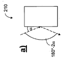
図2のa)〜c)の概略図は、再帰反射器のそのような既知の機能原理を説明するものである。 The schematics of FIGS. 2a)-c) illustrate such known functional principles of retroreflectors.
入射光線の方向に対して傾斜される際、それぞれの反射光線の方向に敏感な反応を示す単純な平面鏡210(図2a)とは対照的に、図2bに示す、相互に固定された角度(本例では90°)で配置された2つの反射面220a,220bを有する再帰反射器220では、第2反射面で反射される光線の方向は第1反射面220aに入射する際の入射方向とは関係なく維持される。
In contrast to the simple plane mirror 210 (FIG. 2a), which reacts sensitively to the direction of each reflected ray when tilted with respect to the direction of the incident ray, the mutually fixed angles shown in FIG. 2b (FIG. 2a). In the
第2反射面に反射する光線方向のこのような維持は、2つの反射面の直角配置(すなわち180°の反射)に限定されず、それぞれの光線を連続的に反射させる2つの表面の間の、他の(一定の)角度において実現される。そのため、2つの反射面230a,230bを有する図2cに示す鏡体230の移動中であっても、第1反射面230aに入射する前の光線の1つの同じ入射方向に対するそれぞれの出射光線(すなわち第2反射面230bで反射される光線)の方向は維持されるか、または一定のままである。
This maintenance of the direction of the rays reflected by the second reflecting surface is not limited to the perpendicular arrangement of the two reflecting surfaces (ie 180 ° reflection), but between the two surfaces that continuously reflect each ray. , Realized at other (constant) angles. Therefore, even while the
上述の考察に基づき、本発明は、特に、リソグラフィプロセス中の相対位置が変わらない、投影レンズ内の2つの反射面を実現する概念を含む。これは、図3に示す例示的実施形態を参照して以下に説明するように、特に(ただし本発明をそれに限定することなく)、2つの反射面を相互に機械的に剛結合する、またはこれらを1つの同じ鏡体にモノリシックに実現することによって達成することができる。 Based on the above considerations, the present invention specifically includes the concept of realizing two reflective surfaces in a projection lens where their relative positions do not change during the lithography process. It mechanically rigidly couples the two reflective surfaces to each other, in particular (but without limiting the invention), as described below with reference to the exemplary embodiments shown in FIG. These can be achieved by monolithically realizing one and the same mirror body.
図3は、上述の概念を実現させるための、2つの反射面311,312を有する鏡体310の構成を示し、同図に略的に示す様に、作動中に入射する光線はそれぞれの場合において2度連続して反射される(この場合、上述の様に、ミラーを有する投影レンズの像面またはウエハ面の下流に生成される像の位置は、鏡体310の移動に関係なく変化しない)。
FIG. 3 shows the configuration of a
また図3は、2つの反射面311,312を有する鏡体310のフレーム305に対する位置が位置センサ320によって測定され、アクチュエータ330を介してコントローラによって(設定点位置の値301に応じて)所望の値に設定される制御ループを示す。位置センサ320、アクチュエータ330およびコントローラ340は、図3の概略図において1自由度のみ、すなわち図面の平面に対して垂直に走る回転軸を中心とする回転運動に対してのみ作用する。技術的には、通常、複数の自由度を同時に操作することができる。
Further, in FIG. 3, the position of the
更なる実施形態において、複数の自由度を測定するために複数の位置センサ320を設けることも可能である。
In a further embodiment, it is also possible to provide a plurality of
ウエハ面に最終的に生成される像位置が収差補正のために行われる鏡体310の動きと関係なく維持されるという事実は、位置センサ320(または複数の位置センサ)が比較的低い測定精度を必要とするようになるという結果をもたらす。この精度は、単一の反射面が移動する際に像位置の安定性を確保しなければならない類似の方法で使用される位置センサの測定精度と比較すると、かなり低いものである。
The fact that the image position finally generated on the wafer surface is maintained regardless of the movement of the
換言すれば、位置センサ320の機能に関しては、収差に影響を及ぼすような鏡体310の位置決めに対しては、比較的粗い位置測定を行えば十分である。この位置測定には収差に影響を及ぼすために必要とされる位置決めに対応する大きな測定範囲(例えば50μm)が必要であるが、移動する1つの反射面のみで反射する場合の像安定性を確保する位置センサと比較して、数桁低い測定精度が要求される。
In other words, regarding the function of the
そのため、センサ技術や制御工学に関するコストが大幅に削減され、そしてその結果、図3に示す構造における鏡体310、アクチュエータ330およびフレーム305の構造的に動的な設計に対する要求が低減される。
As a result, the costs associated with sensor technology and control engineering are significantly reduced, and as a result, the requirements for structurally dynamic design of the
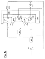
既に述べた様に、本発明は、同じ鏡体上の2つの連続する反射または反射面の実現、または他の方法で実現されるそれぞれの反射面の機械的剛結合に限定されない。更なる実施形態において、それぞれが反射面を有し、相互に剛結合されていない2つの別個の鏡体の相対位置を、適切な制御ループ内において制御することができる。この場合も、図4を参照して以下に詳述するように、センサ技術および制御工学のコストに関する大きな利点がある。 As already mentioned, the present invention is not limited to the realization of two consecutive reflective or reflective surfaces on the same mirror, or the mechanical rigid coupling of each reflective surface realized in other ways. In a further embodiment, the relative positions of two separate mirror bodies, each having a reflective surface and not rigidly coupled to each other, can be controlled within an appropriate control loop. Again, there are significant cost advantages for sensor technology and control engineering, as detailed below with reference to FIG.
図4は2つの個々の鏡体410a,410bを示し、鏡体はそれぞれ反射面411,412を有し、これらの鏡体は相互に機械的に剛結合されていない。2つの鏡体410a,410bの相対位置は相対センサ425によって決定される。(2つの鏡体410a,410bまたは反射面411,412の相対移動は直接的に大きな像の動きをもたらす可能性があるので、)相対センサ425には比較的高い測定精度が必要とされるが、(反射面411,412は連続して同じ角度で配置されたままであるため)、当該相対センサには高い測定範囲が必要とされない。
FIG. 4 shows two
相対位置センサ425の測定信号に基づき、コントローラ445を有する制御ループにおいて、2つの鏡体410a,410bまたは2つの反射面411,412の相対位置は、それぞれの鏡体410a,410bに割り当てられた相対コントローラ445およびアクチュエータ431,432を用いて制御される。この場合、アクチュエータ431,432は、例えば鏡体410a,410bが相互に離れる望ましくない移動の場合、鏡体410a,410bに再びお互いの方に向かって動き出すような力が加えられるように駆動される。
Based on the measurement signal of the
第1アクチュエータ431によってかけられる力をf1,第2アクチュエータ432によってかけられる力をf2,作動変数または共通制御ループの力をfc,差動制御ループの作動変数をfdとすると、
f1 =fc+fd (1)
f2 =fc−fd (2)
となる。
F 1 the force exerted by the
f 1 = f c + f d (1)
f 2 = f c −f d (2)
Will be.
(2つの鏡体410a,410b間の相対位置に関与する)コントローラ445を有する制御ループに加え、図4によれば、外部フレーム405に対する2つの鏡体410aおよび410bの共通位置または平均位置を制御するコントローラ440を有する上位制御ループが実現さる。「401」は設定点位置の値を示す。この場合、
qc= q1 + 1/2 * qd (3)
となり、q1は第1鏡体410aの位置、qcは2つの鏡体410a,410bの共通位置、qdは2つの鏡体410a,410bの相対位置を示す。
In addition to the control loop having the controller 445 (which is involved in the relative position between the two
q c = q 1 + 1/2 * q d (3)
Therefore, q 1 indicates the position of the first mirror bodies 410a, q c indicates the common position of the two
コントローラ440を有する当該上位制御ループは(この点に関しては図3の例示的実施形態と同様に)、大きな測定範囲を有するセンサを必要とするが、同時に、必要とする測定精度は低い(というのもこの場合、例えば、収差を操作するための鏡体410a,410bの傾斜は比較的低い精度で、しかも例えば50μmを超える広い測定範囲にわたって決定しなければならない)。
The superior control loop with controller 440 (similar to the exemplary embodiment of FIG. 3 in this regard) requires a sensor with a large measurement range, but at the same time requires low measurement accuracy. In this case, for example, the inclination of the
本発明は図4に示すようなアクチュエータの具体的な配置に限定されない。更なる実施形態において、例えば、片方のアクチュエータを2つの鏡体410a,410bの間で作用させ、もう片方のアクチュエータを鏡体410a,410bのうちの1つとフレーム405との間で作用させることも可能である。
The present invention is not limited to the specific arrangement of the actuator as shown in FIG. In a further embodiment, for example, one actuator may act between the two
その結果、図4の例示的実施形態を実現するため、2つの制御ループのそれぞれにおいて適用可能なセンサ技術および制御工学に関する(特に、比較的小さな測定範囲にわたって高い測定精度を持つセンサ、および比較的大きな測定範囲にわたって低い測定精度を持つ別のセンサの)要求事項を比較的容易に実現させることができる。 As a result, in order to realize the exemplary embodiment of FIG. 4, the sensor technology and control engineering applicable in each of the two control loops (particularly, a sensor having high measurement accuracy over a relatively small measurement range, and a relatively small measurement range). The requirements (of another sensor with low measurement accuracy over a large measurement range) can be achieved relatively easily.
図5a〜5dは本発明の更なる実施形態を説明する概略図であり、同じ構成部品または同じ機能を持つ構成部品は、図4に示す番号に「100」を加えた番号で示している。 5a to 5d are schematic views illustrating a further embodiment of the present invention, and the same component or the component having the same function is indicated by a number obtained by adding "100" to the number shown in FIG.
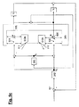
図5aの実施形態は図4の実施形態と以下の点、すなわち、外フレームに対する1つの鏡体のみの位置を測定する代わりに、鏡体510a,510bの両方の平均位置を測定し、これが2つの鏡体510a,510bの外フレーム505に対する平均位置を制御するコントローラを有するそれぞれの上位制御ループの基準として用いられる点で異なる。「501」は設定点位置の値を示す。
The embodiment of FIG. 5a measures the following points with the embodiment of FIG. 4, that is, instead of measuring the position of only one mirror body with respect to the outer frame, the average position of both
図5bに示すコントローラ545を有する制御ループに関しては、鏡体510a,510bの相互位置の測定およびそれぞれの制御は図4と同様であるが、図4とは対照的に、外フレーム505に対する1つの鏡体510bの位置を測定し、これがコントローラ540を有する制御ループの基準として用いられる。コントローラは鏡体510bの位置を制御する。鏡体510aの位置はコントローラ545によって間接的に制御される。
For the control loop with the
図5cの実施形態は図4の実施形態と、外フレーム505に対する鏡体510a,510bのそれぞれの位置が測定される点で異なる。これらの測定位置は、両方の制御ループ、すなわち鏡体510a,510bの共通位置または平均位置を制御するコントローラ540を有する制御ループ、および反射面511,512または鏡体510a, 510bの相対位置をそれぞれ制御するコントローラ545を有する制御ループに使用される。
The embodiment of FIG. 5c differs from the embodiment of FIG. 4 in that the positions of the
図5dに係る実施形態は図4の実施形態と、測定対象物、2つの鏡体510a,510bの相対位置、外フレーム505に対する1つの鏡体510bの位置に関して同様である。しかし図4とは異なり、鏡体510a,510bの位置はコントローラ550または560を有する別個の制御ループでそれぞれ制御される。
The embodiment according to FIG. 5d is the same as that of the embodiment of FIG. 4, regarding the object to be measured, the relative positions of the two
図6は、本発明を実現することのできる投影レンズ600の例示的かつ具体的な配置を示す。しかしながら本発明は図6に示す具体的な配置の投影レンズでの実現に限定されない。更なる例示的実施形態において、本発明は(例えば独国特許出願第102012202675(A1)号明細書に開示されているような)異なる配置の投影レンズまたは他の光学系でも実現することができる。図6の例示的実施形態による投影レンズ600はM1〜M8の8つのミラーを有し、その中のM1,M4,M7およびM8のミラーは照明光の垂直入射(入射角45°未満)用のミラーとして実現され、モリブデン(Mo)およびシリコン(Si)層からなる積層反射層を構成することができる。ミラーM2,M3,M5およびM6は照明光のかすり入射(60°より大きい入射角)用のミラーとして実現され、例えば、モリブデン(Mo)またはルテニウム(Ru)から成る層で被覆することができる。
FIG. 6 shows an exemplary and specific arrangement of the
ほんの一例として、本発明における、その間の相対位置が安定している反射面を、ミラーM5,M6の光学有効面(かすり入射下で反射する2つの面の組み合わせ)、またはミラーM3,M4の光学有効面(かすり入射下で反射する面とほぼ垂直の入射で反射する面との組み合わせ)とすることができる。 As just one example, in the present invention, the reflective surfaces whose relative positions are stable between them are the optically effective surfaces of the mirrors M5 and M6 (combination of the two surfaces reflected under the shaving incident), or the optics of the mirrors M3 and M4. It can be an effective surface (a combination of a surface that reflects under a shaving incident and a surface that reflects at a substantially vertical incident).
本発明を特定の実施形態に基づいて説明してきたが、個々の実施形態の特徴の組み合わせおよび/または交換による多くの変形および代替実施形態が当業者にとって明らかである。従って、そのような変形および代替実施形態が本発明に含まれ、本発明の範囲が添付の特許請求項およびその等価物の観点からのみ限定されることは当業者にとって明らかであろう。 Although the present invention has been described on the basis of specific embodiments, many modifications and alternative embodiments by combining and / or exchanging the features of the individual embodiments will be apparent to those skilled in the art. Thus, it will be apparent to those skilled in the art that such modifications and alternative embodiments are included in the invention and the scope of the invention is limited only in the context of the appended claims and their equivalents.
Claims (16)
‐前記光学系の光線経路に配置され、前記光学系の作動中に発生する収差を補正するために移動可能な第1反射面(311,411,511)と、
‐前記光学系の前記光線経路に配置された少なくとも1つの第2反射面(312,412,512)とを有し、
‐前記光学系は、前記第1反射面(311,411,511)の移動中、前記第1反射面(311,411,511)および前記第2反射面(312,412,512)の相対位置が安定して維持可能であるように構成され、
‐前記第1反射面(311,411,511)および前記第2反射面(312,412,512)は前記光線経路内で直接的に相互に連続する、または前記第1反射面(311,411,511)と前記第2反射面(312,412,512)との間には反射光学素子のみが存在し、
‐前記第1反射面(411,511)および前記第2反射面(412,512)は別個の鏡体に実現され、
基準位置に対する前記第1反射面(311,411,511)および前記第2反射面(312,412,512)の共通位置を制御する第1制御ループを有する光学系。 A microswitch lithographic projection exposure apparatus optical system for,
-A first reflective surface (311, 411, 511) that is located in the light path of the optical system and can be moved to correct aberrations that occur during operation of the optical system.
-Has at least one second reflective surface (312, 421, 512) located in the ray path of the optical system.
-The optical system is in a relative position between the first reflective surface (311, 411, 511) and the second reflective surface (312, 421, 512) while the first reflective surface (311, 411,511) is moving. Is configured to be stable and sustainable,
-The first reflective surface (311, 411, 511) and the second reflective surface (312, 421, 512) are directly continuous with each other in the light path, or the first reflective surface (311, 411). , 511) and the second reflecting surface (312, 421, 512), only a reflecting optical element exists.
-The first reflecting surface (411,511) and the second reflecting surface (421,512) are realized in separate mirror bodies .
Wherein the reference position first reflecting surface (311,411,511) and the optical system that having a first control loop for controlling the common position of the second reflecting surface (312,412,512).
基準位置に対する前記第1反射面(311,411,511)および前記第2反射面(312,412,512)の共通位置を第1制御ループ内で制御し、
前記第1反射面(411,511)と前記第2反射面(412,512)との相対位置を第2制御ループ内で制御する作動方法。
A microswitch lithographic projection exposure apparatus operating method of the optical system for the first reflecting surface in the optical system in the ray path (311,411,511) and at least one second reflecting surface (312,412,512 The first reflecting surface (311, 411,511) is moved to correct the aberration generated during the operation of the optical system, and the first reflecting surface (311, 411,511) is moved during the movement. ) And the second reflecting surface (312, 421, 512) are kept stable, and the first reflecting surface (311, 411, 511) and the second reflecting surface (312, 421, 512) are maintained. Are directly continuous with each other in the ray path, or only reflective optics are between the first reflective surface (311, 411, 511) and the second reflective surface (312, 421, 512). Exists and
The common position of the first reflecting surface (311, 411, 511) and the second reflecting surface (312, 421, 512) with respect to the reference position is controlled in the first control loop.
An operation method in which the relative positions of the first reflecting surface (411,511) and the second reflecting surface (421,512) are controlled in the second control loop.
Applications Claiming Priority (3)
| Application Number | Priority Date | Filing Date | Title |
|---|---|---|---|
| DE102015225262.0A DE102015225262A1 (en) | 2015-12-15 | 2015-12-15 | Optical system, in particular for a microlithographic projection exposure apparatus |
| DE102015225262.0 | 2015-12-15 | ||
| PCT/EP2016/080498 WO2017102599A1 (en) | 2015-12-15 | 2016-12-09 | Optical system, in particular for a microlithographic projection exposure apparatus |
Publications (3)
| Publication Number | Publication Date |
|---|---|
| JP2019505825A JP2019505825A (en) | 2019-02-28 |
| JP2019505825A5 JP2019505825A5 (en) | 2020-01-30 |
| JP6864685B2 true JP6864685B2 (en) | 2021-04-28 |
Family
ID=57680209
Family Applications (1)
| Application Number | Title | Priority Date | Filing Date |
|---|---|---|---|
| JP2018526111A Active JP6864685B2 (en) | 2015-12-15 | 2016-12-09 | Optical system especially for microlithography projection exposure equipment |
Country Status (6)
| Country | Link |
|---|---|
| US (1) | US10838306B2 (en) |
| JP (1) | JP6864685B2 (en) |
| KR (1) | KR20180093923A (en) |
| DE (1) | DE102015225262A1 (en) |
| TW (1) | TWI720087B (en) |
| WO (1) | WO2017102599A1 (en) |
Families Citing this family (1)
| Publication number | Priority date | Publication date | Assignee | Title |
|---|---|---|---|---|
| CN114236970A (en) | 2016-05-25 | 2022-03-25 | 卡尔蔡司Smt有限责任公司 | Position measurement of optical elements in a lithographic apparatus |
Family Cites Families (26)
| Publication number | Priority date | Publication date | Assignee | Title |
|---|---|---|---|---|
| JP2001215718A (en) * | 1999-11-26 | 2001-08-10 | Nikon Corp | Exposure system and exposure method |
| JP2002231619A (en) * | 2000-11-29 | 2002-08-16 | Nikon Corp | Optical illumination equipment and aligner equipped with the same |
| DE10118047A1 (en) | 2001-04-11 | 2002-10-17 | Zeiss Carl | Catadioptric objective, especially for microlithography, has deflection mirrors with mirror surfaces arranged on common base body whose position in objective can be adjusted |
| DE10204465A1 (en) | 2002-02-05 | 2003-08-14 | Zeiss Carl Smt Ag | Method for correcting vibration-induced aberrations in a lens |
| CA2482155A1 (en) * | 2002-04-11 | 2003-10-16 | Heidelberg Instruments Mikrotechnik Gmbh | Method and device for imaging a mask onto a substrate |
| JP2004266264A (en) * | 2003-02-13 | 2004-09-24 | Canon Inc | Optical system, aligner, method for manufacturing device |
| US7126671B2 (en) * | 2003-04-04 | 2006-10-24 | Asml Netherlands B.V. | Lithographic apparatus and device manufacturing method |
| JP2006140366A (en) * | 2004-11-15 | 2006-06-01 | Nikon Corp | Projection optical system and exposure device |
| US7283210B2 (en) * | 2005-03-22 | 2007-10-16 | Nikon Corporation | Image shift optic for optical system |
| DE102006003375A1 (en) * | 2006-01-24 | 2007-08-09 | Carl Zeiss Smt Ag | Group corrected lens |
| JP2007317713A (en) * | 2006-05-23 | 2007-12-06 | Canon Inc | Optical element driving device |
| DE102006034755A1 (en) * | 2006-07-24 | 2008-01-31 | Carl Zeiss Smt Ag | Optical device and method for correcting or improving the imaging behavior of an optical device |
| WO2008040494A1 (en) * | 2006-10-02 | 2008-04-10 | Carl Zeiss Smt Ag | Method for improving the imaging properties of an optical system, and such an optical system |
| CN101548240B (en) * | 2006-12-01 | 2014-09-17 | 卡尔蔡司Smt有限责任公司 | Optical system with an exchangeable, manipulable correction arrangement for reducing image aberrations |
| US20090042115A1 (en) | 2007-04-10 | 2009-02-12 | Nikon Corporation | Exposure apparatus, exposure method, and electronic device manufacturing method |
| JP4986754B2 (en) | 2007-07-27 | 2012-07-25 | キヤノン株式会社 | Illumination optical system and exposure apparatus having the same |
| EP2238513B1 (en) * | 2007-12-21 | 2011-11-02 | Carl Zeiss SMT GmbH | Illumination method |
| US20110001945A1 (en) * | 2009-07-01 | 2011-01-06 | Masayuki Shiraishi | Projection optical system, exposure apparatus, and assembly method thereof |
| JP5767221B2 (en) | 2009-08-07 | 2015-08-19 | カール・ツァイス・エスエムティー・ゲーエムベーハー | Method of manufacturing mirror having at least two mirror surfaces, mirror of projection exposure apparatus for microlithography, and projection exposure apparatus |
| DE102011087851A1 (en) | 2010-12-22 | 2012-06-28 | Carl Zeiss Smt Gmbh | Closure device for a lithographic device and lithographic device |
| NL2007498A (en) | 2010-12-23 | 2012-06-27 | Asml Netherlands Bv | Lithographic apparatus and method of modifying a beam of radiation within a lithographic apparatus. |
| WO2012097833A1 (en) * | 2011-01-20 | 2012-07-26 | Carl Zeiss Smt Gmbh | Method of operating a projection exposure tool |
| DE102012202675A1 (en) | 2012-02-22 | 2013-01-31 | Carl Zeiss Smt Gmbh | Imaging optics for use in optical system of projection exposure system, has imaging lights carrying components and mirror for grazing incidence of imaging light, where mirror for touching incident is arranged in image beam path |
| DE102012212064A1 (en) | 2012-07-11 | 2014-01-16 | Carl Zeiss Smt Gmbh | Lithographic plant with segmented mirror |
| JP2014120682A (en) * | 2012-12-18 | 2014-06-30 | Canon Inc | Exposure device, exposure method and method of manufacturing device |
| DE102014208770A1 (en) * | 2013-07-29 | 2015-01-29 | Carl Zeiss Smt Gmbh | Projection optics for imaging an object field in an image field and projection exposure apparatus with such a projection optics |
-
2015
- 2015-12-15 DE DE102015225262.0A patent/DE102015225262A1/en not_active Ceased
-
2016
- 2016-12-09 WO PCT/EP2016/080498 patent/WO2017102599A1/en active Application Filing
- 2016-12-09 JP JP2018526111A patent/JP6864685B2/en active Active
- 2016-12-09 KR KR1020187016448A patent/KR20180093923A/en not_active Application Discontinuation
- 2016-12-12 TW TW105141037A patent/TWI720087B/en active
-
2018
- 2018-05-01 US US15/968,270 patent/US10838306B2/en active Active
Also Published As
| Publication number | Publication date |
|---|---|
| WO2017102599A1 (en) | 2017-06-22 |
| US20180246416A1 (en) | 2018-08-30 |
| TW201732344A (en) | 2017-09-16 |
| KR20180093923A (en) | 2018-08-22 |
| TWI720087B (en) | 2021-03-01 |
| DE102015225262A1 (en) | 2017-06-22 |
| US10838306B2 (en) | 2020-11-17 |
| JP2019505825A (en) | 2019-02-28 |
Similar Documents
| Publication | Publication Date | Title |
|---|---|---|
| JP5727005B2 (en) | Optical system and multifaceted mirror | |
| JP5684412B2 (en) | Catadioptric projection objective with pupil mirror, projection exposure apparatus and method | |
| JP3931039B2 (en) | Lithographic projection apparatus and device manufacturing method using the same | |
| US9348234B2 (en) | Microlithographic apparatus | |
| US9052606B2 (en) | Microlithographic projection exposure apparatus | |
| US10761429B2 (en) | Projection exposure method and projection exposure apparatus for microlithography | |
| JP6985935B2 (en) | Projection lens with wavefront manipulator, projection exposure method, and projection exposure device | |
| JP2007049165A (en) | Device manufacturing method using lithography apparatus and metrology system | |
| US7643150B2 (en) | Optical apparatus, exposure apparatus, and device manufacturing method | |
| JP2005175177A (en) | Optical apparatus and aligner | |
| JP6864685B2 (en) | Optical system especially for microlithography projection exposure equipment | |
| JP6238177B2 (en) | Projection exposure apparatus having highly flexible manipulator | |
| WO2013175835A1 (en) | Reflector, projection optical system, exposure apparatus, and device manufacturing method | |
| CN106030412B (en) | Illumination system of a microlithographic projection exposure apparatus and method for operating such a system | |
| KR20210035181A (en) | Method and device for determining the heating state of an optical element in an optical system for microlithography | |
| KR20110059721A (en) | Microlithography projection exposure apparatus having at least two operating states | |
| JP2005276933A (en) | Optical member holding device, optical unit and aligner | |
| US7177059B2 (en) | Device and method for manipulation and routing of a metrology beam | |
| JP2019505825A5 (en) |
Legal Events
| Date | Code | Title | Description |
|---|---|---|---|
| A521 | Request for written amendment filed |
Free format text: JAPANESE INTERMEDIATE CODE: A523 Effective date: 20191209 |
|
| A621 | Written request for application examination |
Free format text: JAPANESE INTERMEDIATE CODE: A621 Effective date: 20191209 |
|
| A977 | Report on retrieval |
Free format text: JAPANESE INTERMEDIATE CODE: A971007 Effective date: 20200818 |
|
| A131 | Notification of reasons for refusal |
Free format text: JAPANESE INTERMEDIATE CODE: A131 Effective date: 20200901 |
|
| A601 | Written request for extension of time |
Free format text: JAPANESE INTERMEDIATE CODE: A601 Effective date: 20201117 |
|
| A521 | Request for written amendment filed |
Free format text: JAPANESE INTERMEDIATE CODE: A523 Effective date: 20210217 |
|
| TRDD | Decision of grant or rejection written | ||
| A01 | Written decision to grant a patent or to grant a registration (utility model) |
Free format text: JAPANESE INTERMEDIATE CODE: A01 Effective date: 20210309 |
|
| A61 | First payment of annual fees (during grant procedure) |
Free format text: JAPANESE INTERMEDIATE CODE: A61 Effective date: 20210402 |
|
| R150 | Certificate of patent or registration of utility model |
Ref document number: 6864685 Country of ref document: JP Free format text: JAPANESE INTERMEDIATE CODE: R150 |
|
| R250 | Receipt of annual fees |
Free format text: JAPANESE INTERMEDIATE CODE: R250 |