JP6862470B2 - Power efficient voltage level translator circuit - Google Patents
Power efficient voltage level translator circuit Download PDFInfo
- Publication number
- JP6862470B2 JP6862470B2 JP2018550674A JP2018550674A JP6862470B2 JP 6862470 B2 JP6862470 B2 JP 6862470B2 JP 2018550674 A JP2018550674 A JP 2018550674A JP 2018550674 A JP2018550674 A JP 2018550674A JP 6862470 B2 JP6862470 B2 JP 6862470B2
- Authority
- JP
- Japan
- Prior art keywords
- voltage
- voltage level
- level translator
- bypass
- pull
- Prior art date
- Legal status (The legal status is an assumption and is not a legal conclusion. Google has not performed a legal analysis and makes no representation as to the accuracy of the status listed.)
- Active
Links
Images


Classifications
-
- G—PHYSICS
- G06—COMPUTING; CALCULATING OR COUNTING
- G06F—ELECTRIC DIGITAL DATA PROCESSING
- G06F1/00—Details not covered by groups G06F3/00 - G06F13/00 and G06F21/00
- G06F1/26—Power supply means, e.g. regulation thereof
- G06F1/32—Means for saving power
- G06F1/3203—Power management, i.e. event-based initiation of a power-saving mode
- G06F1/3234—Power saving characterised by the action undertaken
- G06F1/3296—Power saving characterised by the action undertaken by lowering the supply or operating voltage
-
- H—ELECTRICITY
- H03—ELECTRONIC CIRCUITRY
- H03K—PULSE TECHNIQUE
- H03K19/00—Logic circuits, i.e. having at least two inputs acting on one output; Inverting circuits
- H03K19/0008—Arrangements for reducing power consumption
- H03K19/0016—Arrangements for reducing power consumption by using a control or a clock signal, e.g. in order to apply power supply
-
- H—ELECTRICITY
- H03—ELECTRONIC CIRCUITRY
- H03K—PULSE TECHNIQUE
- H03K19/00—Logic circuits, i.e. having at least two inputs acting on one output; Inverting circuits
- H03K19/01—Modifications for accelerating switching
- H03K19/017—Modifications for accelerating switching in field-effect transistor circuits
- H03K19/01707—Modifications for accelerating switching in field-effect transistor circuits in asynchronous circuits
-
- H—ELECTRICITY
- H03—ELECTRONIC CIRCUITRY
- H03K—PULSE TECHNIQUE
- H03K19/00—Logic circuits, i.e. having at least two inputs acting on one output; Inverting circuits
- H03K19/0175—Coupling arrangements; Interface arrangements
- H03K19/0185—Coupling arrangements; Interface arrangements using field effect transistors only
- H03K19/018507—Interface arrangements
- H03K19/018521—Interface arrangements of complementary type, e.g. CMOS
-
- H—ELECTRICITY
- H03—ELECTRONIC CIRCUITRY
- H03K—PULSE TECHNIQUE
- H03K3/00—Circuits for generating electric pulses; Monostable, bistable or multistable circuits
- H03K3/01—Details
- H03K3/012—Modifications of generator to improve response time or to decrease power consumption
-
- H—ELECTRICITY
- H03—ELECTRONIC CIRCUITRY
- H03K—PULSE TECHNIQUE
- H03K3/00—Circuits for generating electric pulses; Monostable, bistable or multistable circuits
- H03K3/02—Generators characterised by the type of circuit or by the means used for producing pulses
- H03K3/353—Generators characterised by the type of circuit or by the means used for producing pulses by the use, as active elements, of field-effect transistors with internal or external positive feedback
- H03K3/356—Bistable circuits
- H03K3/356104—Bistable circuits using complementary field-effect transistors
- H03K3/356113—Bistable circuits using complementary field-effect transistors using additional transistors in the input circuit
- H03K3/35613—Bistable circuits using complementary field-effect transistors using additional transistors in the input circuit the input circuit having a differential configuration
-
- H—ELECTRICITY
- H03—ELECTRONIC CIRCUITRY
- H03K—PULSE TECHNIQUE
- H03K3/00—Circuits for generating electric pulses; Monostable, bistable or multistable circuits
- H03K3/02—Generators characterised by the type of circuit or by the means used for producing pulses
- H03K3/353—Generators characterised by the type of circuit or by the means used for producing pulses by the use, as active elements, of field-effect transistors with internal or external positive feedback
- H03K3/356—Bistable circuits
- H03K3/356104—Bistable circuits using complementary field-effect transistors
- H03K3/356113—Bistable circuits using complementary field-effect transistors using additional transistors in the input circuit
- H03K3/356147—Bistable circuits using complementary field-effect transistors using additional transistors in the input circuit using pass gates
-
- Y—GENERAL TAGGING OF NEW TECHNOLOGICAL DEVELOPMENTS; GENERAL TAGGING OF CROSS-SECTIONAL TECHNOLOGIES SPANNING OVER SEVERAL SECTIONS OF THE IPC; TECHNICAL SUBJECTS COVERED BY FORMER USPC CROSS-REFERENCE ART COLLECTIONS [XRACs] AND DIGESTS
- Y02—TECHNOLOGIES OR APPLICATIONS FOR MITIGATION OR ADAPTATION AGAINST CLIMATE CHANGE
- Y02D—CLIMATE CHANGE MITIGATION TECHNOLOGIES IN INFORMATION AND COMMUNICATION TECHNOLOGIES [ICT], I.E. INFORMATION AND COMMUNICATION TECHNOLOGIES AIMING AT THE REDUCTION OF THEIR OWN ENERGY USE
- Y02D10/00—Energy efficient computing, e.g. low power processors, power management or thermal management
Description
[0001] 開示される態様は、処理システムのための電圧供給(voltage supply)に関する。より具体的には、実例的な態様は、第1の電圧領域と第2の電圧領域との間の電圧レベル変換(voltage level translation)のための、電力効率のよい電圧レベルトランスレータ回路(voltage level translator circuit)を対象とする。 [0001] The disclosed embodiment relates to a voltage supply for a processing system. More specifically, an exemplary embodiment is a power efficient voltage level translator circuit for voltage level translation between a first voltage region and a second voltage region. The translator circuit) is targeted.
[0002] 現代の処理システム(例えば、システムオンチップすなわち「SOC」)は、異なる周波数および電力条件(power considerations)を有することができる様々なサブシステムまたは構成要素を含み得る。これに対応して、SOCの異なる区画には、異なる供給電圧(supply voltage)が提供され得る。例えば、メモリシステムは、より高い供給電圧が供給され得るメモリセル(例えば、スタティックランダムアクセスメモリすなわち「SRAM」セル)を含み得るのに対して、中央処理ユニット(CPU)またはプロセッサコアの論理セルは、より低い供給電圧をサポートできる。従って、SOCは、2つ以上の電圧アイランドまたは電圧領域(例えば、論理電圧領域、メモリ電圧領域、等)を用いて設計され得、対応する電圧供給を有する各電圧領域は、電圧領域における構成要素(例えば、論理セル、メモリセル、等)の電圧条件(voltage considerations)に適合するように合わせられる。 [0002] Modern processing systems (eg, system-on-chip or "SOC") may include various subsystems or components that can have different frequency and power considerations. Correspondingly, different compartments of SOC may be provided with different supply voltages. For example, a memory system can include memory cells that can be supplied with higher supply voltages (eg, static random access memory or "SRAM" cells), whereas central processing unit (CPU) or processor core logic cells. , Can support lower supply voltage. Thus, the SOC may be designed with two or more voltage islands or voltage regions (eg, logic voltage region, memory voltage region, etc.), and each voltage region with the corresponding voltage supply is a component in the voltage region. It is adjusted to meet the voltage considerations of (eg, logic cells, memory cells, etc.).
[0003] 2つの電圧領域を渡る信号があり得、例えば、論理電圧領域におけるCPUによってメモリ電圧領域におけるメモリシステムに発行される読込みまたは書込みコマンドである。このような信号のために、本技術分野では「電圧レベルトランスレータ」として知られている変換回路(translation circuit)が、第1の電圧領域から第2の電圧領域への信号を変換するために提供され得る。しかしながら、いくつかのケースでは、1つまたは複数の電圧領域の電圧は動的にスケーリングされ得、これは、第1および第2の電圧領域の供給電圧が同等または実質的に同じになることをもたらし得る(例えば、これは本技術分野で既知である「ターボモード」において行われ、ここにおいて、論理電圧領域の以前の低い供給電圧は、より高い周波数で論理セルを動作させるためにより高い供給電圧にスケーリングされ得、論理電圧領域のより高い供給電圧は、メモリ電圧領域の供給電圧と実質的に同じであり得る)。このようなケースでは、第1および第2の電圧領域の供給電圧が実質的に同じであるので、第1の電圧領域と第2の電圧領域との間に電圧レベルトランスレータの必要はないことになる。 [0003] There can be a signal across two voltage regions, for example a read or write command issued by the CPU in the logical voltage region to the memory system in the memory voltage region. For such signals, a translation circuit, known in the art as a "voltage level translator", provides to translate the signal from the first voltage region to the second voltage region. Can be done. However, in some cases, the voltage in one or more voltage regions can be dynamically scaled, which means that the supply voltages in the first and second voltage regions are equal or substantially the same. It can result (eg, this is done in "turbo mode" known in the art, where the previously lower supply voltage in the logic voltage region is the higher supply voltage to operate the logic cell at higher frequencies. The higher supply voltage in the logic voltage region can be substantially the same as the supply voltage in the memory voltage region). In such cases, the supply voltages in the first and second voltage regions are substantially the same, so there is no need for a voltage level translator between the first and second voltage regions. Become.
[0004] しかしながら、従来の設計では、電圧レベルトランスレータはそれにもかかわらずアクティブのままであり、第1および第2の電圧領域の供給電圧が実質的に同じである場合でも、第1の電圧領域と第2の電圧領域との間の信号の電圧変換を不必要に実行し得る。アクティブのままであり、信号の経路内に留まることによって、電圧レベルトランスレータは電力を消費し、電圧レベル変換が必要ないときでも常に信号の経路に遅延を付加する。 [0004] However, in conventional designs, the voltage level translator nevertheless remains active, even though the supply voltages in the first and second voltage regions are substantially the same. The voltage conversion of the signal between and the second voltage region may be unnecessarily performed. By remaining active and staying in the signal path, the voltage level translator consumes power and always adds a delay to the signal path even when no voltage level conversion is required.
[0005] 本発明の実例的な態様は、電力効率のよい電圧レベルトランスレータのためのシステムおよび方法を対象とする。第1の電圧領域の第1の供給電圧と第2の電圧領域の第2の供給電圧が異なる通常モードでは、電圧レベルトランスレータは、第1の電圧領域における入力信号を第2の電圧領域における出力信号に変換する。第1の供給電圧と第2の供給電圧が実質的に同じであるバイパスモードでは、バイパス回路(bypass circuit)は、電圧レベルトランスレータをバイパスし、入力信号を第1の電圧領域における出力信号として供給するように構成され、よって、バイパスモードで電圧レベルトランスレータによって挿入される遅延を回避する。さらに、パワーダウン回路(power-down circuit)が、バイパスモードでは電圧レベルトランスレータをパワーダウンするが、通常モードではパワーダウンしないように構成される。 [0005] Illustrative embodiments of the present invention are directed to systems and methods for power efficient voltage level translators. In normal mode, where the first supply voltage in the first voltage region and the second supply voltage in the second voltage region are different, the voltage level translator outputs the input signal in the first voltage region to the output in the second voltage region. Convert to a signal. In bypass mode, where the first supply voltage and the second supply voltage are substantially the same, the bypass circuit bypasses the voltage level translator and feeds the input signal as an output signal in the first voltage region. It is configured to avoid the delay inserted by the voltage level translator in bypass mode. In addition, a power-down circuit is configured to power down the voltage level translator in bypass mode but not in normal mode.
[0006] 例えば、実例的な態様は、第1の電圧領域の第1の供給電圧が第2の電圧領域の第2の供給電圧とは異なる通常モードでは、前記第1の電圧領域における入力信号を前記第2の電圧領域における出力信号に変換するように構成された電圧レベルトランスレータと、前記第1の供給電圧と前記第2の供給電圧が実質的に同じであるバイパスモードでは、前記電圧レベルトランスレータをバイパスし、前記入力信号を前記第1の電圧領域における前記出力信号として供給するように構成されたバイパス回路と、前記バイパスモードでは前記電圧レベルトランスレータをパワーダウンするが、前記通常モードではパワーダウンしないように構成されたパワーダウン回路と、を備える装置を対象とする。 [0006] For example, in an exemplary embodiment, in a normal mode in which the first supply voltage in the first voltage region is different from the second supply voltage in the second voltage region, the input signal in the first voltage region. In a voltage level translator configured to convert the voltage to an output signal in the second voltage region and in bypass mode where the first supply voltage and the second supply voltage are substantially the same, the voltage level. A bypass circuit configured to bypass the translator and supply the input signal as the output signal in the first voltage region, and power down the voltage level translator in the bypass mode but power in the normal mode. The target is a device including a power-down circuit configured so as not to go down.
[0007] 別の実例的な態様は、電圧レベル変換の方法を対象とし、前記方法は、電圧レベルトランスレータにおいて、第1の電圧領域の第1の供給電圧が第2の電圧領域の第2の供給電圧とは異なる通常モードでは、前記第1の電圧領域における入力信号を前記第2の電圧領域における出力信号に変換することと、前記第1の供給電圧と前記第2の供給電圧が実質的に同じであるバイパスモードでは、前記電圧レベルトランスレータをバイパスし、前記入力信号を前記第1の電圧領域における前記出力信号として供給することと、前記バイパスモードでは前記電圧レベルトランスレータをパワーダウンするが、前記通常モードではパワーダウンしないことと、を備える。 [0007] Another exemplary embodiment is directed to a method of voltage level conversion, wherein in a voltage level translator, the first supply voltage in the first voltage region is the second in the second voltage region. In a normal mode different from the supply voltage, the input signal in the first voltage region is converted into the output signal in the second voltage region, and the first supply voltage and the second supply voltage are substantially. In the bypass mode, which is the same as, the voltage level translator is bypassed and the input signal is supplied as the output signal in the first voltage region, and in the bypass mode, the voltage level translator is powered down. It is provided that the power is not reduced in the normal mode.
[0008] さらに別の実例的な態様は、第1の電圧領域の第1の供給電圧が第2の電圧領域の第2の供給電圧とは異なる通常モードでは、前記第1の電圧領域における入力信号を前記第2の電圧領域における出力信号に変換するための手段と、前記第1の供給電圧と前記第2の供給電圧が実質的に同じであるバイパスモードでは、変換するための前記手段をバイパスし、前記第1の電圧領域における前記出力信号を供給するための手段と、前記バイパスモードでは前記電圧レベルトランスレータをパワーダウンするが、前記通常モードではパワーダウンしないための手段と、を備える装置を対象とする。 [0008] Yet another exemplary embodiment is that in normal mode, where the first supply voltage in the first voltage region is different from the second supply voltage in the second voltage region, the input in the first voltage region. The means for converting a signal into an output signal in the second voltage region and the means for converting in a bypass mode in which the first supply voltage and the second supply voltage are substantially the same. A device including means for bypassing and supplying the output signal in the first voltage region, and means for powering down the voltage level translator in the bypass mode but not in the normal mode. Is targeted.
[0009] 添付の図面は、本発明の態様の説明を助けるために提示されており、それら態様の限定ではなく、その例示のためだけに提供されている。 [0009] The accompanying drawings are presented to aid in the description of aspects of the invention and are provided solely for illustration purposes, not limitation of those aspects.
[0014] 本発明の態様は、本発明の特定の態様に向けられた以下の説明および関連の図面で開示される。代替の態様が、本発明の範囲から逸脱することなく考案され得る。追加的に、本発明の周知の要素は、本発明の関連する詳細を曖昧にしないように、詳細には説明されないかまたは省略されるであろう。 [0014] Aspects of the invention are disclosed in the following description and related drawings directed to a particular aspect of the invention. Alternative embodiments can be devised without departing from the scope of the invention. Additionally, well-known elements of the invention will not be described or omitted in detail so as not to obscure the relevant details of the invention.
[0015] 「実例的な」という用語は、本明細書では、「例、事例、または例示としての役割を果たす」という意味で使用されている。「実例的な」ものとして、本明細書で説明される任意の態様は、必ずしも他の態様に対して好ましいまたは有利なものとして解釈されるべきではない。同様に、「本発明の態様」という用語は、本発明の全ての態様が、説明される特徴、利点、または動作モードを含むことを必要としない。 [0015] The term "exemplary" is used herein to mean "act as an example, case, or example." As "exemplary", any aspect described herein should not necessarily be construed as favorable or advantageous over other aspects. Similarly, the term "aspects of the invention" does not require that all aspects of the invention include the features, advantages, or modes of operation described.
[0016] 本明細書で使用される専門用語は、特定の態様を説明することのみを目的としたものであり、本発明の態様を限定することを意図したものではない。本明細書で使用されるとき、単数形「a」、「an」、および「the」は、別途コンテキストから明らかに示されていない限り、複数形もまた含むように意図されている。「備える」、「備えている」、「含む」、および/または「含んでいる」という用語は、本明細書で使用されるとき、記述された特徴、整数、ステップ、動作、要素、および/または構成要素の存在を指定するが、1つまたは複数の他の特徴、整数、ステップ、動作、要素、構成要素、および/またはそれらのグループの存在または追加を妨げないことがさらに理解されるであろう。 [0016] The terminology used herein is for the purpose of describing particular embodiments only and is not intended to limit aspects of the invention. As used herein, the singular forms "a," "an," and "the" are also intended to include the plural, unless explicitly indicated in the context. The terms "provide," "provide," "include," and / or "include," as used herein, describe features, integers, steps, actions, elements, and /. Or it is further understood that it specifies the existence of a component, but does not prevent the existence or addition of one or more other features, integers, steps, behaviors, elements, components, and / or groups thereof. There will be.
[0017] さらに、多くの態様が、例えば、コンピューティングデバイスの要素によって実行されることになるアクションのシーケンスの観点から説明される。本明細書で説明される様々なアクションが、特定の回路(例えば、特定用途向け集積回路(ASIC))によって、1つまたは複数のプロセッサによって実行されているプログラム命令によって、または両方の組合せによって、行われることができることが認識されるであろう。追加的に、本明細書で説明されるこれらのアクションのシーケンスは、実行時に、関連したプロセッサに本明細書で説明される機能を行わせることになるコンピュータ命令の対応のセットを記憶した任意の形態のコンピュータ可読記憶媒体内で全体的に具現化されるものと考えられることができる。よって、本発明の様々な態様は、いくつかの異なる形態で具現化され得、それらの全ては、特許請求される主題の範囲内にあるものと企図されている。加えて、本明細書で説明される態様の各々に関して、任意のそのような態様の対応する形態は、例えば、説明されているアクションを行う「ように構成された論理」として、本明細書では説明され得る。 [0017] Further, many aspects are described, for example, in terms of the sequence of actions that will be performed by the elements of the computing device. The various actions described herein are performed by a particular circuit (eg, an application specific integrated circuit (ASIC)), by program instructions executed by one or more processors, or by a combination of both. It will be recognized that it can be done. In addition, the sequence of these actions described herein stores any set of correspondences of computer instructions that, at run time, would cause the associated processor to perform the functions described herein. It can be considered to be embodied as a whole within the form of computer-readable storage medium. Thus, various aspects of the invention can be embodied in several different forms, all of which are intended to be within the claims. In addition, with respect to each of the aspects described herein, the corresponding form of any such aspect is described herein as, for example, as "logic configured to" perform the actions described. Can be explained.
[0018] 本開示の実例的な態様は、第1の電圧領域から第2の電圧領域への信号を変換するように構成された電圧レベルトランスレータを対象としている。第1の電圧領域が第2の電圧領域と同等である場合には、第1の電圧領域と第2の電圧領域との間の信号の経路に電圧レベルトランスレータによって挿入される遅延を回避するために電圧レベルトランスレータをバイパスするための、選択的なバイパス回路が含まれる。さらに、実例的な態様では、上記の方式で電圧レベルトランスレータがバイパスされるとき、電圧レベルトランスレータをパワーダウンまたはシャットオフ(shut off)するための、電力制御回路が含まれ得る。よって、実例的な態様では、信号の経路内に電圧レベルトランスレータが必要ではないとき、電圧レベルトランスレータに関連する電力消費と遅延が回避され得る。これらの態様および関連する態様が、以下のセクションで、図を参照してこれから説明される。 An exemplary embodiment of the present disclosure is directed to a voltage level translator configured to convert a signal from a first voltage region to a second voltage region. When the first voltage region is equivalent to the second voltage region, to avoid the delay inserted by the voltage level translator in the signal path between the first voltage region and the second voltage region. Includes a selective bypass circuit for bypassing the voltage level translator. Further, in an exemplary embodiment, a power control circuit may be included to power down or shut off the voltage level translator when the voltage level translator is bypassed in the manner described above. Thus, in an exemplary embodiment, the power consumption and delay associated with a voltage level translator can be avoided when no voltage level translator is required in the signal path. These and related aspects will be described in the sections below with reference to the figures.
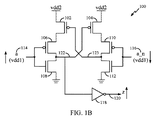
[0019] 最初に、図1A〜図1Bを参照して、従来の電圧レベルトランスレータ100が説明される。電圧レベルトランスレータ100は、第1の供給電圧VDD1によって供給される第1の電圧領域における相補的な入力信号a114およびa_n116を、第2の供給電圧VDD2によって供給される第2の電圧領域における出力信号z120に変換するように構成される。一般性の喪失なく、第1の供給電圧VDD1は、通常の動作条件下では第2の電圧供給VDD2よりも少ないこともあるが、いくつかの事例では、第1および第2の電圧供給VDD1およびVDD2は、実質的に同じ電圧値であり得る。第1および第2の電圧供給VDD1およびVDD2が異なる値を想定し得る特定の条件、またはこれらの電圧供給が生成される方式は本考察に密接に関連しないが、一例は、論理セルを有する処理システムのプロセッサコアまたは同様のものを備える第1の電圧領域、ここで第1の電圧供給VDD1が論理供給電圧と称され得る、第1の電圧領域と、メモリセルを有するメモリシステムを備える第2の電圧領域、ここで第2の電圧供給VDD2がメモリ供給電圧と称され得る、第2の電圧領域と、に関係する場合もある。
[0019] First, the conventional
[0020] 図1A〜図1Bに例示されている構成では、電圧レベルトランスレータ100は、p型金属酸化物半導体(PMOS)デバイスまたはp型電界効果トランジスタ(PFET)で構成され得る、プルアップトランジスタ(pull-up transistor)102および104と、n型金属酸化物半導体(NMOS)デバイスまたはn型電界効果トランジスタ(NFET)で構成され得るプルダウントランジスタ(pull-down transistor)108および112と、PMOSデバイスまたはPFETとして構成され得るプルアップトランジスタ106および110を備える。相補的な入力信号a114およびa_n116の電圧レベル変換の出力は、ノード122から導出され得、通過されるインバータ118が出力信号z120を供給できる。図1A〜図1Bに例示されているような電圧レベルトランスレータ100の動作可能な詳細が周知であるが、いくつかの簡単な詳細が以下のセクションで提供され、本開示の実例的な態様が適用され得る、電圧レベルトランスレータの他の様々な構成が可能であることに留意されたい。
[0020] In the configurations illustrated in FIGS. 1A-1B, the
[0021] 図1Aを参照すると、入力信号a114が立ち上がる、または低論理状態(例えば、バイナリ「0」)から高論理状態(例えば、バイナリ「1」)に遷移し、これに対応して入力信号a_n116が立ち下がるケースが例示されている。これに対応して、第1段階では、プルアップトランジスタ106はシャットオフし始め、プルダウントランジスタ108はオンになり始めることになり、これは、ノード122を放電し始める。一方、入力信号a_n116は立ち下がり、プルアップトランジスタ110をオンにしながらプルダウントランジスタ112をシャットオフする。一旦ノード122が十分に低い値に立ち下がると、第2段階では、プルアップトランジスタ104がオンになり、プルアップトランジスタ104および110はノード123を第2の供給電圧VDD2にチャージし始める。
[0021] With reference to FIG. 1A, the input signal a114 rises or transitions from a low logic state (eg, binary "0") to a high logic state (eg, binary "1"), and the corresponding input signal. A case where a_n116 falls down is illustrated. Correspondingly, in the first stage, the pull-up
[0022] ノード123がチャージし終わる(charge up)と、プルアップトランジスタ102はシャットオフし始め、それは、プルダウントランジスタ108がノード122をさらにプルダウンするのを助ける。プルダウンされるノード122は、プルアップトランジスタ104がオンにされるプロセスを助け、これはさらにノード123をチャージする。最終的には、プルアップトランジスタ102は完全にシャットオフされ、ノード122は「0」の論理状態に遷移するが、ノード123は第2の電圧領域において論理「1」に遷移する。ノード122および123は、相補的な入力信号a114およびa_n116の値にその後の変化が起きるまで、それらの「0」および「1」の論理状態を維持する。
[0022] When the
[0023] よって、インバータ118を通過した後、ノード122のインバートされた値は、第2の電圧領域において立ち上がる出力信号z120として現れ、第1の電圧領域における入力信号a114の立ち上がりと入力信号a_n116の立ち下がりに対応する。電圧レベルトランスレータ100の上記段階は、相補的な入力信号a114およびa_n116と出力信号z120との間の経路に、対応する遅延またはレイテンシを挿入する。
Therefore, after passing through the
[0024] ここで図1Bを参照して、入力信号a114が立ち下がりa_n116が立ち上がる、反対のシナリオがこれから説明される。このケースでは、プルアップトランジスタ110はシャットオフし始め、プルダウントランジスタ112はオンになり始めることになり、よって、ノード123を放電する。一方、入力信号a114が立ち下がると、プルダウントランジスタ108は、プルアップトランジスタ106をオンにしながら、シャットオフされることを引き起こされる。一旦ノード123が十分に低い値に立ち下がると、第2段階では、プルアップトランジスタ102がオンになり、プルアップトランジスタ102および106はノード122を第2の供給電圧VDD2にチャージし始める。ノード122がチャージし終わると、プルアップトランジスタ104はシャットオフさせられ、それは、プルダウントランジスタ112がノード123をさらにプルダウンするのに役立つ。プルダウンされるノード123は、プルアップトランジスタ102がオンにされるのを助け、これはさらにノード122をチャージする。最終的には、プルアップトランジスタ104は完全にシャットオフし、ノード123は「0」の論理状態に遷移するが、ノード122は第2の電圧領域において「1」の論理状態に遷移する。ノード122の論理状態は、第2の電圧領域において、立ち下がり出力信号z120として現れるように、インバータ118によってインバートされる。ノード122および123は、相補的な入力信号a114およびa_n116上にその後の変化が生じるまで、それらの「1」および「0」の論理状態をそれぞれ維持する。図に示すように、このケースでの電圧レベルトランスレータ100の動作に関わる上記段階もまた、著しい遅延を引き起こす。
[0024] Now, with reference to FIG. 1B, the opposite scenario in which the input signal a114 falls and a_n116 rises will be described. In this case, the pull-up
[0025] 第1および第2の供給電圧VDD1およびVDD2の電圧値間の差が大きいケースの場合、電圧レベルトランスレータ100の左側にあるプルアップトランジスタ102および106のスタックは、入力信号a114が立ち上がり(またはlowからhighに遷移し)、これに対応して入力信号a_n116が立ち下がる(またはhighからlowに遷移する)ケースの場合に、プルダウントランジスタ108が例えばノード122を効率的にプルダウンすることを可能にするために、弱められ得る。同様に、電圧レベルトランスレータ100の右側にあるプルアップトランジスタ104および110のスタックは、入力信号a114が立ち下がり、これに対応して入力信号a_n116が立ち上がるケースの場合、プルダウントランジスタ112が効率的にノード123をプルダウンすることを可能にするために、弱められ得る。このプルダウントランジスタおよびプルアップトランジスタの相対的なサイジングは、相補的な入力信号a114およびa_n116ならびに出力信号z120からの遅延をさらに増大させ得る。
[0025] In the case where the difference between the voltage values of the first and second supply voltages VDD1 and VDD2 is large, the input signal a114 rises in the stack of the pull-up
[0026] 電圧レベルトランスレータ100の上記考察から、図1A〜図1Bに示される両方のケースでは、かなりの遅延が挿入されることが理解され得る。さらに、様々なプルアップおよびプルダウントランジスタをオンにしたりオフにしたりする複数の段階もまた電力を消費する。第1の電圧領域の第1の電圧供給VDD1と第2の電圧領域の第2の電圧供給VDD2が実質的に同じである場合、図2A〜図2Bを参照してこれから説明される実例的な態様では、電圧レベルトランスレータ100に関連する遅延および電力は回避され得る。
From the above considerations of the
[0027] 図2Aを参照すると、回路200が示されており、これは、電圧レベルトランスレータ250およびバイパス回路252を備える。電圧レベルトランスレータ250は、図1A〜図1Bを参照して説明された従来の電圧レベルトランスレータ100と同様であるように構成され得るか、または第1の電圧供給VDD1によって供給される第1の電圧領域における相補的な入力信号a214およびa_n216を、第2の電圧供給VDD2によって供給される第2の電圧領域におけるノード222において導出される中間出力信号y_nに変換するのに好適な他の任意の電圧レベルトランスレータ構成であり得る。一例となる態様では、第1の電圧領域は、論理セルを備える論理電圧領域に対応し、第2の電圧領域は、メモリセルを備えるメモリ電圧領域に対応する。
[0027] With reference to FIG. 2A,
[0028] 電圧レベルトランスレータ250の構成が電圧レベルトランスレータ100の構成と同様である態様では、電圧レベルトランスレータ250の構成要素は、電圧レベルトランスレータ100の対応する構成要素と同様の機能性を有し得るので、電圧レベルトランスレータ250の動作可能な詳細は、簡潔さのために繰り返されない。簡単に、電圧レベルトランスレータ250の、プルアップトランジスタ202、204、206、210、およびプルダウントランジスタ208、212は、電圧レベルトランスレータ100の対応するプルアップトランジスタ102、104、106、110、およびプルダウントランジスタ108、112と同様に構成され得る。従って、ノード222および223は、図1A〜図1Bで説明されたような相補的な入力信号a114およびa_n116の立ち上がりと立ち下がりに基づくノード122および123と同様の方式で、相補的な入力信号a214およびa_n216の立ち上がりと立ち下がりに基づいて第2の電圧領域に変換される電圧を受け取り得る。
[0028] In an embodiment in which the configuration of the
[0029] さらに、回路200は、いくつかの動作モードを伴い得る。例えば、通常の動作モードは、第1の電圧供給VDD1が第2の電圧供給VDD2とは異なる(例えば、それよりも少ないまたは多い)状況を含むと定義され得、相補的な入力信号a214およびa_n216の第1の電圧領域から第2の電圧領域への電圧レベル変換が望まれる。通常モードでは、電圧レベルトランスレータ250の機能性は、電圧レベルトランスレータ100の機能性と実質的に同様であり得る。
[0029] Further, the
[0030] 回路200の第2の動作モードはバイパスモードと定義され、ここにおいて、第1の電圧供給VDD1は、第2の電圧供給VDD2と実質的に同じであるので、相補的な入力信号a214およびa_n216の第1の電圧領域から第2の電圧領域への電圧レベル変換は、バイパスモードでは回避され得る。バイパスモードは、例えば、前述したターボモードに対応し得、ここにおいて、第1の電圧領域(例えば、論理電圧領域)および第2の電圧領域(例えば、メモリ電圧領域)の供給電圧が同等または実質的に同じであり得る。このコンテキストでは、実質的に同等とは、オフにされるべきである高い方の電圧領域におけるデバイスが、望まないリーク電流を引き起こすほどオンにならないように、第1の電圧領域と第2の電圧領域との間の電圧差が十分小さいものと当業者によって理解されるであろう。バイパスモードでは、バイパス回路252が電圧レベルトランスレータ250をバイパスするために用いられ得、それにより、電圧レベルトランスレータ250を横断する相補的な入力信号a214およびa_n216によって生じ得る遅延を回避する。
[0030] The second operating mode of the
[0031] いくつかの態様では、バイパス回路252は、バイパスモードでは入力信号a_n216をバイパス回路252の出力として選択し、通常モードでは、中間信号y_nとして現れるノード222をバイパス回路252の出力として選択するためのセレクタまたはマルチプレクサとして実装され得る。この目的のために、バイパス回路252は、各々がPFETとNFETデバイスの並列結合によって形成される、2つの送信ゲート回路234および236を含み得る。信号bypass232は、回路200がバイパスモードで動作されることになる場合にアサートされ得る。bypass232の補数が、信号bypass_n230として示されている。bypass232がhighである場合、bypass_n230はlowであり、送信ゲート回路234はバイパス回路252の出力にa_n216を渡すためにオンにされる。これに対して、bypass232がlowである場合、bypass_n230はhighであり、送信ゲート回路236は、バイパス回路252の出力に中間信号y_n(すなわち、ノード222)を渡すためにオンにされる。バイパス回路252の出力は、回路200の出力信号z220として現れるようにインバータ218によってインバートされる。従って、バイパスモードでは(例えば、第1および第2の供給電圧VDD1およびVDD2が実質的に同じであることに基づいてbypass232がアサートされるとき)、電圧レベルトランスレータ250および対応する遅延を完全にバイパスしながら、a_n216がバイパス回路252の出力として選択され得る。
[0031] In some embodiments, the
[0032] 図2B〜図2Dは、バイパスモードでの電力節約のために使用され得るパワーダウン回路に関する実例的な態様を例示している。パワーダウン回路は、以下のセクションで詳細に説明されるように、bypass232がアサートされ、電圧レベルトランスレータ250がバイパスされるときに選択的に展開(deploy)され得る。
[0032] FIGS. 2B-2D illustrate exemplary embodiments of power-down circuits that can be used to save power in bypass mode. The power-down circuit can be selectively deployed when bypass232 is asserted and the
[0033] 最初に図2Bを参照すると、バイパスモードでの電力節約の実例的な態様による、回路270が例示されている。回路270は、図2Aの回路200に追加されたパワーダウン回路275を含む。より詳細には、回路270もまた、上記図2Aを参照して説明された電圧レベルトランスレータ250およびバイパス回路252を含み、パワーダウン回路275は、示されているように電圧レベルトランスレータ250に結合される。バイパスモードでは、つまりbypass232がアサートされたとき、パワーダウン回路275は、電圧レベルトランスレータ250を選択的にパワーダウンするように構成される。しかし通常モードでは、つまりbypass232がアサートされないとき(または言い換えると、bypass_n230がアサートされたとき)、パワーダウン回路275は、通常動作のために電圧レベルトランスレータ250をアクティブに保つ。パワーダウン回路275は、以下でさらに詳細に説明される。
[0033] First, with reference to FIG. 2B,
[0034] 示されているように、パワーダウン回路275は、第1のプルダウントランジスタ240(例えば、NMOSトランジスタまたはNFET)を含む。第1のプルダウントランジスタ240は、電圧レベルトランスレータ250のプルダウントランジスタ208および212の各々に、およびグラウンドに直列に接続され、第1のプルダウントランジスタ240のゲートはbypass_n230によって制御される。よって、通常モードでは、つまりbypass232がアサートされずbypass_n230がアサートされたとき、第1のプルダウントランジスタ240がオンにされ、これは、プルダウントランジスタ208および212のソース端子をグラウンドに接続し、よって、電圧レベルトランスレータ250の通常構成を保持する、または言い換えると、電圧レベルトランスレータ250がアクティブに留まることを引き起こす。これに対して、バイパスモードでは、bypass232がアサートされ、bypass_n230をlowに駆動させ、第1のプルダウントランジスタ240をオフにし、次に、プルダウントランジスタ208および212についてのグラウンドまでの経路をゲートオフし(gating off)、電圧レベルトランスレータ250をパワーダウンさせる。
[0034] As shown, the power-
[0035] パワーダウン回路275はまた、第1のプルアップトランジスタ242(例えば、PMOSトランジスタまたはPFET)を含むことができるが、これはオプションであり得る。パワーダウン回路275に含まれるとき、第1のプルアップトランジスタ242は、電圧レベルトランスレータ250の中間信号y_n(またはノード222)に、および第2の供給電圧VDD2に接続され、第1のプルアップトランジスタ242のゲートもまた、bypass_n230によって制御される。通常モードでは、bypass232はlowであり、bypass_n230がアサートされ、よって、第1のプルアップトランジスタ242をオフにし、これは、電圧レベルトランスレータ250の通常構成に影響を及ぼさない。これに対して、バイパスモードでは、bypass232がアサートされ、bypass_n230をlowに駆動させ、第1のプルアップトランジスタ242をオンにし、よって、ノード222を第2の供給電圧VDD2に接続し、プルアップトランジスタ204をオフにする。それゆえ、第1のプルアップトランジスタ242は、含まれるとき、(ノード222を第2の供給電圧VDD2に接続することによって)バイパスモードでノード222がフロート(float)することを引き起こさないと考えられ、これは、バイパス回路252における反結合(back coupling)の低減につながり、それにより、バイパスモードでの回路270のパフォーマンスを向上させる。これに対応して、バイパスモードでは、第2の電圧供給VDD2からプルアップトランジスタ210およびプルダウントランジスタ212への電力供給もまたカットオフされる。
[0035] The power-
[0036] よって、bypass_n230がアサートされたときのバイパスモードで、第1のプルダウントランジスタ240をオフにすることと第1のプルアップトランジスタ242をオンにすることの複合効果は、電力供給から電圧レベルトランスレータ250のスイッチングトランジスタを全て分離することであり、よって、電圧レベルトランスレータ250をパワーダウンする。従って、電圧レベルトランスレータ250がバイパスされるとき(例えば、第1および第2の供給電圧VDD1およびVDD2が実質的に同じであるとき)、電圧レベルトランスレータ250はパワーダウンもされ、電力節約をもたらす。
Therefore, in the bypass mode when bypass_n230 is asserted, the combined effect of turning off the first pull-
[0037] パワーダウン回路275が第1のプルアップトランジスタ242を含まないケースでは、ノード222に結合された中間信号y_nは、バイパスモードの間フロートさせられることになるが、先述されたように第1のプルダウントランジスタ240がゲートオフされることになるので、電圧レベルトランスレータ250は、依然としてパワーダウンされたままであることになる。パワーダウン回路275に第1のプルアップトランジスタ242を含まないことは、パワーダウン回路275に関連する面積を低減させ得る。
[0037] In the case where the power-
[0038] 次に、図2Cを参照すると、バイパスモードでの電力節約の別の実例的な態様による、回路280が例示されている。回路270のように、回路280もまた、図2Aの回路200に追加された、このケースではパワーダウン回路285と特定されている、パワーダウン回路を含む。より詳細には、回路280もまた、上記図2Aを参照して説明された電圧レベルトランスレータ250およびバイパス回路252を含み、パワーダウン回路285は、示されているように電圧レベルトランスレータ250に結合される。バイパスモードでは、つまりbypass232がアサートされたとき、パワーダウン回路285は、電圧レベルトランスレータ250を選択的にパワーダウンするように構成される。しかし通常モードでは、つまりbypass232がアサートされないとき(または言い換えると、bypass_n230がアサートされたとき)、パワーダウン回路285は、通常動作のために電圧レベルトランスレータ250をアクティブに保つ。パワーダウン回路285は、以下でさらに詳細に説明される。
[0038] Next, with reference to FIG. 2C,
[0039] 示されているように、パワーダウン回路285は、第2の供給電圧VDD2と電圧レベルトランスレータ250との間に(例えば、示されているように、電圧レベルトランスレータ250のプルアップトランジスタ202および204に)結合された第2のプルアップトランジスタ282を含み、第2のプルアップトランジスタ282のゲートはbypass232によって制御される。バイパスモードでは、つまりbypass232がhighであるとき、第2のプルアップトランジスタ282はオフにされ、よって、第2の供給電圧VDD2から電圧レベルトランスレータ250への電圧供給をゲートオフし、ノード222および信号y_nがフロートすることを引き起こす。そうでない場合、通常モードでは、bypass232はlowであり、第2のプルアップトランジスタ282をオンにさせ、通常通り第2の供給電圧VDD2を電圧レベルトランスレータ250に接続する。
As shown, the power-
[0040] パワーダウン回路285は、オプションとして、電圧レベルトランスレータ250のノード222に接続された第2のプルダウントランジスタ284(例えば、NMOSトランジスタまたはNFET)を含むことができ、第2のプルダウントランジスタ284のゲートは、bypass232によって制御される。第2のプルダウントランジスタ284がこの方式で構成されるとき、バイパスモードでは、つまりbypass232がhighであるとき、第2のプルダウントランジスタ284はオンにされ、ノード222または信号y_nをグラウンドまたは論理「0」に接続する。それゆえ、第2のプルダウントランジスタ284はまた、ノード222がバイパスモードでフロートすることを防ぐことができ、バイパス回路252における反結合を低減し、それによって、バイパスモードでの回路280のパフォーマンスを向上させる。通常モードでは、bypass232はlowであり、第2のプルダウントランジスタ284をオフにさせ、ノード222または信号y_nに対するいずれの影響も除去する。
[0040] The power-
[0041] これから図2Dを参照すると、バイパスモードでの電力節約のさらに別の実例的な態様による、回路290が例示されている。回路270および280のように、回路290もまた、図2Aの回路200に追加された、このケースではパワーダウン回路295と特定されている、パワーダウン回路を含む。より詳細には、回路290もまた、上記図2Aを参照して説明された電圧レベルトランスレータ250およびバイパス回路252を含み、パワーダウン回路295は、示されているように電圧レベルトランスレータ250に結合される。バイパスモードでは、つまりbypass232がアサートされたとき、パワーダウン回路295は、電圧レベルトランスレータ250を選択的にパワーダウンするように構成される。しかし通常モードでは、つまりbypass232がアサートされないとき(または言い換えると、bypass_n230がアサートされたとき)、パワーダウン回路295は、通常動作のために電圧レベルトランスレータ250をアクティブに保つ。パワーダウン回路295は、以下でさらに詳細に説明される。
[0041] With reference to FIG. 2D,
[0042] 示されているように、パワーダウン回路295はまた、上述されたパワーダウン回路285の第2のプルアップトランジスタ282と同様に構成され、かつ第2の供給電圧VDD2と電圧レベルトランスレータ250との間に(例えば、示されているように、電圧レベルトランスレータ250のプルアップトランジスタ202および204に)結合された第2のプルアップトランジスタ282を含み、第2のプルアップトランジスタ282のゲートはbypass232によって制御される。バイパスモードでは、つまりbypass232がhighであるとき、第2のプルアップトランジスタ282は同様にオフにされ、よって、第2の供給電圧VDD2から電圧レベルトランスレータ250への電圧供給をゲートオフし、ノード222および信号y_nがフロートすることを引き起こす。そうでない場合、通常モードでは、bypass232はlowであり、第2のプルアップトランジスタ282をオンにさせ、通常通り第2の供給電圧VDD2を電圧レベルトランスレータ250に結合させる。
As shown, the power-
[0043] パワーダウン回路295はまた、電圧レベルトランスレータ250とグラウンドとの間に結合された第3のプルダウントランジスタ294も含み、第3のプルダウントランジスタ294のゲートはbypass_n230によって制御される。バイパスモードでは、つまりbypass_n230がlowであるとき、第3のプルダウントランジスタ294はオフにされ、よって、電圧レベルトランスレータ250のためのグラウンドまでの経路をゲートオフする。そうではない場合、通常モードでは、bypass_n230がhighであり、第3のプルダウントランジスタ294をオンにさせ、電圧レベルトランスレータ250を通常通りグラウンドに結合させる。
[0043] The power-
[0044] パワーダウン回路295は、オプションとして、電圧レベルトランスレータ250のノード222に接続された、第4のプルダウントランジスタ296または第4のプルアップトランジスタ298という2つのうちの1つを含むことができるが、両方ではない。第4のプルダウントランジスタ296がパワーダウン回路295に含まれる場合、第4のプルダウントランジスタ296のゲートは、bypass232によって制御される。バイパスモードでは、つまりbypass232がhighであるとき、第4のプルダウントランジスタ296はオンにされ、よって、ノード222をグラウンドまたは論理「0」に接続する。通常モードでは、bypass232はlowであり、第4のプルダウントランジスタ296をオフにさせ、ノード222または信号y_nに対するいずれの影響も除去する。
[0044] The power-
[0045] これに対して、第4のプルアップトランジスタ298がパワーダウン回路295に含まれる場合、第4のプルアップトランジスタ298のゲートはbypass_n230によって制御される。バイパスモードでは、つまりbypass_n230がlowであるとき、第4のプルアップトランジスタ298はオンにされ、よって、ノード222を第2の供給電圧VDD2または論理「1」に接続する。通常モードでは、bypass_n230はhighであり、第4のプルアップトランジスタ298をオフにさせ、ノード222または信号y_nに対するいずれの影響も除去する。認識されるように、第4のプルダウントランジスタ296または第4のプルアップトランジスタ298のうちのいずれか1つが、パワーダウン回路295に含まれ、上記のように構成されるとき、ノード222は、バイパスモードでフロートすることが防がれ、それは、バイパス回路252における反結合の低減につながり、それによって、バイパスモードでの回路290のパフォーマンスを向上させる。
[0045] On the other hand, when the fourth pull-up transistor 298 is included in the power-
[0046] 従って、実例的な態様では、回路270、280、または290のような回路は、電圧レベルトランスレータ250がバイパスモードで使用されないときの電力消費を回避するために、パワーダウン回路275、285、または295それぞれを用いて構成され得る。回路270、280、および290はまた、バイパスモードで電圧レベルトランスレータを通る遅延を回避するためのバイパス回路252も含む。
Thus, in an exemplary embodiment, circuits such as
[0047] 例えばbypass232をアサートするバイパスモードに入る状況は、第1および第2の電圧供給VDD1およびVDD2が実質的に同じ電圧値になることの検出を伴うことができる。この検出は、本技術分野では既知である方法およびシステムを用いて行われることができる。例えば、バッテリで動作するモバイルデバイスのバッテリレベルまたは充電状態が、バイパスモードに入る、またはそれを終了するために使用され得る。例えば、モバイルデバイスが外部電源にプラグインされる場合、またはバッテリレベルが高い(または、ある特定の充電レベルを上回る)場合、モバイルデバイスは、高いパフォーマンスまたはターボモードをサポートするようにプログラミングされ得、ここにおいて、第1および第2の電圧供給VDD1およびVDD2は実質的に同じにされ得る。しかしながら、バッテリレベルが、例えば低バッテリモードまで所定のレベルよりも下がる場合、第1および第2の電圧供給VDD1およびVDD2の別個の電圧レベルが維持され得、バイパスモードは終了し得る。デジタルおよび/またはアナログ回路は、バッテリレベルまたは外部電源への接続を検出して、これに対応してバイパスモードが選択され得るかどうか、または通常動作条件が電圧レベルトランスレータに適用されるかのインジケーションを提供するように構成され得る。いくつかの例では、プログラマまたはオペレーティングシステムが、バイパスモードに入るまたはそれを終了するために使用され得るソフトウェア制御を提供することも可能であり得る。(例えば、bypass232をアサートする)バイパスモードの検出または決定のための他の様々なオプションが当業者によって認識されることになり、従って、本明細書ではさらに詳細には説明されない。 [0047] For example, the situation of entering the bypass mode asserting bypass232 can be accompanied by the detection that the first and second voltage supplies VDD1 and VDD2 have substantially the same voltage value. This detection can be performed using methods and systems known in the art. For example, the battery level or charge state of a battery-powered mobile device can be used to enter or exit bypass mode. For example, if the mobile device is plugged into an external power source, or if the battery level is high (or above a certain charge level), the mobile device can be programmed to support high performance or turbo mode. Here, the first and second voltage supplies VDD1 and VDD2 can be substantially the same. However, if the battery level drops below a predetermined level, for example to low battery mode, the separate voltage levels of the first and second voltage supplies VDD1 and VDD2 can be maintained and the bypass mode can be terminated. Digital and / or analog circuits detect battery level or connection to an external power source and indicate whether bypass mode can be selected correspondingly or whether normal operating conditions apply to the voltage level translator. It can be configured to provide a voltage. In some examples, it may also be possible for the programmer or operating system to provide software control that can be used to enter or exit bypass mode. Various other options for detecting or determining bypass modes (eg, asserting bypass232) will be recognized by those of skill in the art and are therefore not described in further detail herein.
[0048] 実例的な態様が、本明細書で開示されるプロセス、関数、および/またはアルゴリズムを実行するための様々な方法を含むことが認識されるであろう。例えば、図3に例示されているように、実例的な態様は、電圧レベル変換を実行する方法(300)を含むことができる。方法300は、例えば、回路270、280、または290の通常動作モードに関係するブロック302を含むことができ、ブロック303は、例えば、回路270、280、または290のバイパス動作モードに関係できる。図3は、通常モードからバイパスモードに、または場合によってはバイパスモードから通常モードに遷移することが可能であることを示すために、ブロック302および303間に両矢印を示している。これらブロック302および303は、以下でさらに詳細に説明される。
[0048] It will be appreciated that exemplary embodiments include various methods for performing the processes, functions, and / or algorithms disclosed herein. For example, as illustrated in FIG. 3, an exemplary embodiment can include a method (300) of performing a voltage level conversion. The
[0049] 述べたように、ブロック302は、通常動作モードに関係でき、ここにおいて、第1の電圧領域の第1の供給電圧VDD1は、第2の電圧領域の第2の供給電圧VDD2とは異なる。通常モードでは、ブロック302は、例えば電圧レベルトランスレータ250において、第1の電圧領域における入力信号、例えば入力信号a214を、通常モードでは、第2の電圧領域における出力信号、例えば出力信号z220に変換することを含むことができる。
As mentioned, the
[0050] ブロック303は、バイパス動作モードに関係でき、ここにおいて、第1および第2の供給電圧VDD1およびVDD2は、実質的に同じである。ブロック303は、同時に実行され得るブロック304および306を備えることができる。
[0050]
[0051] 従って、ブロック304は、バイパスモードでは電圧レベルトランスレータをバイパスすることと、入力信号を第1の電圧領域における出力信号として供給することとを含むことができる。例えば、ブロック304は、bypass232がアサートされたときにバイパス回路252を使用して電圧レベルトランスレータ250をバイパスすることと、入力信号を第1の電圧領域における出力信号として供給することとを含むことができる。
[0051] Thus, block 304 can include bypassing the voltage level translator in bypass mode and supplying the input signal as an output signal in the first voltage region. For example, the
[0052] ブロック306は、バイパスモードでは電圧レベルトランスレータを選択的にパワーダウンすることを含むことができる。例えば、ブロック306は、(例えば、回路270、280、または290についての実装形態が実例的な態様で選ばれるかどうかに依存してパワーダウン回路275、285、または295を使用して)電圧レベルトランスレータ250をパワーダウンすることを含むことができる。具体的には、本明細書で説明されているパワーダウン技法のいずれかを使用して、電圧レベルトランスレータ250は、バイパスモードでは(bypass232がhighであり、bypass_n230がlowであるとき)、パワーダウンされ得、電圧レベルトランスレータ250は、通常モードでは(bypass232がlowであり、bypass_n230がhighであるとき)、アクティブに維持され得る。この方式で、方法300は、bypass232がアサートされたときのバイパスモードで回路270、280、または290における電圧レベルトランスレータ250に関連する遅延および電力を回避するために使用され得る。
[0052]
[0053] これから図4を参照すると、電力効率のよい電圧レベル変換のための回路270、280、または290のような回路を含むコンピューティングデバイスの特定の例示的な態様のブロック図が図示されており、概して400と指定されている。コンピューティングデバイス400は、上記図3を参照して説明された方法300を実行するための機能性を含み得る。さらに、いくつかの態様では、コンピューティングデバイス400は、ワイヤレス通信デバイスとして構成され得る。
[0053] With reference to FIG. 4, a block diagram of a particular exemplary embodiment of a computing device, including circuits such as
[0054] コンピューティングデバイス400は、プロセッサ464およびメモリ432を含むように示されている。いくつかの態様では、プロセッサ464は、第1の供給電圧VDD1を有する第1の電圧領域または論理電圧領域に属し得、メモリ432は、第2の供給電圧VDD2を有する第2の電圧領域またはメモリ電圧領域に属し得る。従って、上記図2B〜図2Dを参照して説明された回路270、280、または290の概略図は、プロセッサ464とメモリ432との間で構成されると示されている。回路270/280/290は、通常モードでは、電圧レベルトランスレータ250を使用して、例えば入力信号a214(例えば、プロセッサ464からメモリ432への読取り/書込みコマンドに対応)の、出力信号z220への電圧レベル変換を行い得る。回路270/280/290は、バイパスモードでは、バイパス回路252および対応するパワーダウン回路275/285/295を使用して電圧レベルトランスレータ250をバイパスおよびパワーダウンして、電圧レベル変換を伴わずに、プロセッサ464からの相補的な入力信号a214およびa_n216を、出力信号z220としてメモリ432に供給するように構成され得、ここにおいて、第1および第2の供給電圧VDD1およびVDD2は、バイパスモードでは実質的に同じである。前述されたように、バイパスモードは、本技術分野で既知のターボモードに対応し得る。図4の回路270/280/290の表現は、対応する図2B〜図2Dに示された様々な詳細を、明確さのために省略していることに留意されたい。
[0054] The
[0055] コンピューティングデバイス400はまた、プロセッサ464に、およびディスプレイ428に結合されたディスプレイコントローラ426も備え得る。図4はまた、コンピューティングデバイス400において提供され得るオプションの態様を示す。例えば、コンピューティングデバイスは、オプションとして、プロセッサ464に結合されたコーダ/デコーダ(CODEC)434(例えば、オーディオおよび/または音声CODEC)と、ここで、スピーカ436およびマイクロフォン438がCODEC434に結合され、プロセッサ464に結合された(モデムを含み得る)ワイヤレスコントローラ440とを備え得、ワイヤレスコントローラ440はワイヤレスアンテナ442に結合される。
[0055] The
[0056] 上記オプションとしての特徴のうちの1つまたは複数が存在する一例となる態様では、プロセッサ464、回路270/280/290、メモリ432、CODEC434、ディスプレイコントローラ426、およびワイヤレスコントローラ440は、システムインパッケージまたはシステムオンチップデバイス422に含まれることができる。いくつかの態様では、入力デバイス430および電源444は、システムオンチップデバイス422に結合され得る(いくつかのケースでは、第1および第2の電圧供給VDD1およびVDD2が、電源444から導出または供給され得ることも留意されたい)が、いくつかの態様では、ディスプレイ428、入力デバイス430、スピーカ436、マイクロフォン438、ワイヤレスアンテナ442、および電源444は、システムオンチップデバイス422の外部にあり得る。しかしながら、ディスプレイ428、入力デバイス430、スピーカ436、マイクロフォン438、ワイヤレスアンテナ442、および電源444の各々は、インターフェースまたはコントローラのような、システムオンチップデバイス422の構成要素に結合され得る。
[0056] In an exemplary embodiment in which one or more of the optional features are present, the
[0057] 図4は概してコンピューティングデバイスを図示しているが、プロセッサ464、およびメモリ432はまた、セットトップボックス、ミュージックプレーヤ、ビデオプレーヤ、エンターテインメントユニット、ナビゲーションデバイス、通信デバイス、携帯情報端末(PDA)、固定ロケーションデータユニット、モバイルフォン、サーバ、およびコンピュータへと一体化され得ることが留意されるべきである。
[0057] Although FIG. 4 generally illustrates a computing device, the
[0058] 当業者は、情報および信号が、様々な異なる技術および技法の任意のものを使用して表され得ることを認識するであろう。例えば、上記の説明全体を通して参照され得る、データ、命令、コマンド、情報、信号、ビット、シンボル、およびチップは、電圧、電流、電磁波、磁界または磁気粒子、光場または光粒子、もしくはこれらの任意の組合せによって表わされ得る。 Those skilled in the art will recognize that information and signals can be represented using any of a variety of different techniques and techniques. For example, data, instructions, commands, information, signals, bits, symbols, and chips that may be referenced throughout the above description are voltages, currents, electromagnetic waves, magnetic or magnetic particles, light fields or light particles, or any of these. Can be represented by a combination of.
[0059] さらに当業者は、本明細書で開示された態様に関連して説明された様々な例示的な論理ブロック、モジュール、回路、およびアルゴリズムステップが、電子ハードウェア、コンピュータソフトウェア、またはその両方の組合せとして実装され得ることを認識するであろう。このハードウェアとソフトウェアの互換性を明確に例示するために、様々な例示的なコンポーネント、ブロック、モジュール、回路、およびステップが、概して、それらの機能性の観点から上述されている。このような機能性が、ハードウェアとして実装されるか、ソフトウェアとして実装されるかは、特定の用途およびシステム全体に課せられる設計制約に依存する。当業者は、特定のアプリケーションごとに、説明された機能性を多様な方法で実装できるが、このような実装の判断は本発明の範囲からの逸脱を引き起こすものとして解釈されるべきではない。 In addition, one of ordinary skill in the art will appreciate the various exemplary logical blocks, modules, circuits, and algorithm steps described in connection with aspects disclosed herein, including electronic hardware, computer software, or both. You will recognize that it can be implemented as a combination of. To clearly illustrate this hardware-software compatibility, various exemplary components, blocks, modules, circuits, and steps are generally described above in terms of their functionality. Whether such functionality is implemented as hardware or software depends on the design constraints imposed on the particular application and the entire system. One of ordinary skill in the art can implement the described functionality in a variety of ways for a particular application, but such implementation decisions should not be construed as causing deviations from the scope of the invention.
[0060] 本明細書で開示された態様に関連して説明された方法、シーケンス、および/またはアルゴリズムは、直接的にハードウェアにおいて、プロセッサによって実行されるソフトウェアモジュールにおいて、またはそれら2つの組合せで、具現化され得る。ソフトウェアモジュールは、RAMメモリ、フラッシュメモリ、ROMメモリ、EPROMメモリ、EEPROM(登録商標)メモリ、レジスタ、ハードディスク、リムーバブルディスク、CD−ROM、または当該技術分野で既知の他の任意の形態の記憶媒体に存在し得る。実例的な記憶媒体は、プロセッサが記憶媒体から情報を読み取り、また記憶媒体に情報を書き込むことができるように、プロセッサに結合される。代替として、記憶媒体は、プロセッサと一体であり得る。 [0060] The methods, sequences, and / or algorithms described in connection with aspects disclosed herein are directly in hardware, in software modules executed by a processor, or in combination of the two. , Can be embodied. Software modules can be used in RAM memory, flash memory, ROM memory, EPROM memory, EEPROM® memory, registers, hard disks, removable disks, CD-ROMs, or any other form of storage medium known in the art. Can exist. An exemplary storage medium is coupled to the processor so that the processor can read information from the storage medium and write information to the storage medium. Alternatively, the storage medium can be integrated with the processor.
[0061] 従って、本発明の一態様は、電力効率のよい電圧レベル変換のための方法を具現化するコンピュータ可読媒体を含むことができる。従って、本発明は、例示された例に限定されるわけではなく、本明細書で説明された機能を行うためのあらゆる手段が本発明の態様に含まれる。 [0061] Accordingly, one aspect of the present invention may include a computer-readable medium that embodies a method for power efficient voltage level conversion. Therefore, the present invention is not limited to the exemplified examples, and all means for performing the functions described herein are included in aspects of the present invention.
[0062] 先の開示は、本発明の例示的な態様を示しているが、添付の特許請求の範囲によって定義される本発明の範囲から逸脱することなく、様々な変更および修正が本明細書で行われ得ることが留意されるべきである。本明細書で説明された発明の態様にしたがった方法の請求項の機能、ステップ、および/またはアクションは、任意の特定の順序で行われる必要はない。さらに、本発明の要素は、単数形で説明および特許請求され得るが、単数形に限定することが明記されていない限り、複数形が企図される。
以下に本願発明の当初の特許請求の範囲に記載された発明を付記する。
[C1]
装置であって、
通常モードでは、第1の電圧領域における入力信号を第2の電圧領域における出力信号に変換するように構成された電圧レベルトランスレータと、ここにおいて、前記第1の電圧領域の第1の供給電圧は、前記第2の電圧領域の第2の供給電圧とは異なる、
バイパスモードでは、前記電圧レベルトランスレータをバイパスし、前記入力信号を前記第1の電圧領域における前記出力信号として供給するように構成されたバイパス回路と、ここにおいて、前記第1の供給電圧と前記第2の供給電圧は、実質的に同じである、 前記バイパスモードでは前記電圧レベルトランスレータをパワーダウンするが、前記通常モードではパワーダウンしないように構成されたパワーダウン回路と
を備える、装置。
[C2]
前記パワーダウン回路は、前記バイパスモードでは前記電圧レベルトランスレータへのグラウンド接続をゲートオフするように構成された第1のプルダウントランジスタを備える、C1に記載の装置。
[C3]
前記パワーダウン回路は、前記バイパスモードでは前記電圧レベルトランスレータの出力ノードを前記第2の供給電圧に接続するように構成された第1のプルアップトランジスタをさらに備える、C2に記載の装置。
[C4]
前記パワーダウン回路は、前記バイパスモードでは前記第2の供給電圧と前記電圧レベルトランスレータとの間の接続をゲートオフするように構成された第2のプルアップトランジスタを備える、C1に記載の装置。
[C5]
前記パワーダウン回路は、前記バイパスモードでは前記電圧レベルトランスレータの出力ノードをグラウンドに接続するように構成された第2のプルダウントランジスタをさらに備える、C4に記載の装置。
[C6]
前記パワーダウン回路は、前記バイパスモードでは前記電圧レベルトランスレータとグラウンドとの間の接続をゲートオフするように構成された第3のプルダウントランジスタをさらに備える、C4に記載の装置。
[C7]
前記パワーダウン回路は、前記バイパスモードでは前記電圧レベルトランスレータの出力ノードをグラウンドに接続するように構成された第4のプルダウントランジスタをさらに備える、C6に記載の装置。
[C8]
前記パワーダウン回路は、前記バイパスモードでは前記電圧レベルトランスレータの出力ノードを前記第2の供給電圧に接続するように構成された第4のプルアップトランジスタをさらに備える、C6に記載の装置。
[C9]
前記バイパス回路は、前記バイパスモードでは前記第1の電圧領域における前記入力信号を選択し、前記通常モードでは前記第2の電圧領域における前記電圧レベルトランスレータの出力を選択するように構成されたマルチプレクサを備える、C1に記載の装置。
[C10]
前記第1の電圧領域は、論理セルを備える論理電圧領域に対応し、前記第2の電圧領域は、メモリセルを備えるメモリ電圧領域に対応し、前記バイパスモードは、ターボモードに対応する、C1に記載の装置。
[C11]
セットトップボックス、ミュージックプレーヤ、ビデオプレーヤ、エンターテインメントユニット、ナビゲーションデバイス、通信デバイス、携帯情報端末(PDA)、固定ロケーションデータユニット、サーバ、モバイルフォン、およびコンピュータからなるグループから選択されたデバイスに一体化される、C1に記載の装置。
[C12]
電圧レベル変換の方法であって、
通常モードでは、電圧レベルトランスレータにおいて、第1の電圧領域における入力信号を第2の電圧領域における出力信号に変換することと、ここにおいて、前記第1の電圧領域の第1の供給電圧は、前記第2の電圧領域の第2の供給電圧とは異なる、
バイパスモードでは、前記電圧レベルトランスレータをバイパスし、前記入力信号を前記第1の電圧領域における前記出力信号として供給することと、ここにおいて、前記第1の供給電圧と前記第2の供給電圧は、実質的に同じである、
前記バイパスモードでは前記電圧レベルトランスレータをパワーダウンするが、前記通常モードではパワーダウンしないことと
を備える、方法。
[C13]
前記電圧レベルトランスレータをパワーダウンすることは、前記バイパスモードではグラウンド接続から前記電圧レベルトランスレータをゲートオフするために第1のプルダウントランジスタをオフにすることを備える、C12に記載の方法。
[C14]
前記バイパスモードでは、前記電圧レベルトランスレータの出力ノードを前記第2の供給電圧に接続するために第1のプルアップトランジスタをオンにすることをさらに備える、C13に記載の方法。
[C15]
前記電圧レベルトランスレータをパワーダウンすることは、前記バイパスモードでは前記第2の供給電圧と前記電圧レベルトランスレータとの間の接続をゲートオフするように構成された第2のプルアップトランジスタをオフにすることを備える、C12に記載の方法。
[C16]
前記バイパスモードでは前記電圧レベルトランスレータの出力ノードをグラウンドに接続するために第2のプルダウントランジスタをオンにすることをさらに備える、C15に記載の方法。
[C17]
前記バイパスモードでは前記電圧レベルトランスレータとグラウンドとの間の接続をゲートオフするために第3のプルダウントランジスタをオフにすることをさらに備える、C15に記載の方法。
[C18]
前記バイパスモードでは前記電圧レベルトランスレータの出力ノードをグラウンドに接続するために第4のプルダウントランジスタをオンにすることをさらに備える、C17に記載の方法。
[C19]
前記バイパスモードでは前記電圧レベルトランスレータの出力ノードを前記第2の供給電圧に接続するために第4のプルアップトランジスタをオンにすることをさらに備える、C17に記載の方法。
[C20]
前記バイパスモードでは前記第1の電圧領域における前記入力信号を選択し、前記通常モードでは前記第2の電圧領域における前記電圧レベルトランスレータの出力を選択することを備える、C12に記載の方法。
[C21]
前記第1の電圧領域は、論理セルを備える論理電圧領域に対応し、前記第2の電圧領域は、メモリセルを備えるメモリ電圧領域に対応し、前記バイパスモードは、ターボモードに対応する、C12に記載の方法。
[C22]
装置であって、
通常モードでは、第1の電圧領域における入力信号を第2の電圧領域における出力信号に変換するための手段と、ここにおいて、前記第1の電圧領域の第1の供給電圧は、前記第2の電圧領域の第2の供給電圧とは異なる、
バイパスモードでは、変換するための前記手段をバイパスし、前記第1の電圧領域における前記出力信号を供給するための手段と、ここにおいて、前記第1の供給電圧と前記第2の供給電圧は、実質的に同じである、
前記バイパスモードでは前記電圧レベルトランスレータをパワーダウンするが、前記通常モードではパワーダウンしないための手段と
を備える、装置。
[C23]
前記電圧レベルトランスレータをパワーダウンするための前記手段は、前記バイパスモードではグラウンド接続から前記電圧レベルトランスレータをゲートオフするための手段を備える、C22に記載の装置。
[C24]
前記バイパスモードでは前記電圧レベルトランスレータの出力ノードを前記第2の供給電圧に接続するための手段をさらに備える、C23に記載の装置。
[C25]
前記電圧レベルトランスレータをパワーダウンするための前記手段は、前記バイパスモードでは前記第2の供給電圧と前記電圧レベルトランスレータとの間の接続をゲートオフするための手段を備える、C22に記載の装置。
[C26]
前記バイパスモードでは前記電圧レベルトランスレータの出力ノードをグラウンドに接続するための手段をさらに備える、C25に記載の装置。
[C27]
前記バイパスモードでは前記電圧レベルトランスレータとグラウンドとの間の接続をゲートオフするための手段をさらに備える、C25に記載の装置。
[C28]
前記バイパスモードでは前記電圧レベルトランスレータの出力ノードをグラウンドに接続するための手段をさらに備える、C27に記載の装置。
[C29]
前記バイパスモードでは前記電圧レベルトランスレータの出力ノードを前記第2の供給電圧に接続するための手段をさらに備える、C27に記載の装置。
[C30]
前記バイパスモードでは前記第1の電圧領域における前記入力信号を選択し、前記通常モードでは前記第2の電圧領域における前記電圧レベルトランスレータの出力を選択するための手段をさらに備える、C22に記載の装置。
[0062] The above disclosure illustrates exemplary aspects of the invention, but various modifications and modifications are made herein without departing from the scope of the invention as defined by the appended claims. It should be noted that it can be done in. The functions, steps, and / or actions of the claims of the method according to the aspects of the invention described herein need not be performed in any particular order. In addition, the elements of the invention may be described and claimed in the singular, but the plural is contemplated unless explicitly stated to limit it to the singular.
The inventions described in the original claims of the present invention are described below.
[C1]
It ’s a device,
In the normal mode, the voltage level translator configured to convert the input signal in the first voltage region to the output signal in the second voltage region, and here the first supply voltage in the first voltage region , Different from the second supply voltage in the second voltage region,
In the bypass mode, a bypass circuit configured to bypass the voltage level translator and supply the input signal as the output signal in the first voltage region, and here, the first supply voltage and the first. The supply voltage of 2 is substantially the same as that of a power-down circuit configured to power down the voltage level translator in the bypass mode but not in the normal mode.
A device that comprises.
[C2]
The device according to C1, wherein the power-down circuit comprises a first pull-down transistor configured to gate off the ground connection to the voltage level translator in the bypass mode.
[C3]
The device according to C2, wherein the power-down circuit further comprises a first pull-up transistor configured to connect the output node of the voltage level translator to the second supply voltage in the bypass mode.
[C4]
The device according to C1, wherein the power-down circuit comprises a second pull-up transistor configured to gate off the connection between the second supply voltage and the voltage level translator in the bypass mode.
[C5]
The device according to C4, wherein the power-down circuit further comprises a second pull-down transistor configured to connect the output node of the voltage level translator to ground in the bypass mode.
[C6]
The device according to C4, wherein the power-down circuit further comprises a third pull-down transistor configured to gate off the connection between the voltage level translator and ground in the bypass mode.
[C7]
The device according to C6, wherein the power-down circuit further comprises a fourth pull-down transistor configured to connect the output node of the voltage level translator to ground in the bypass mode.
[C8]
The device according to C6, wherein the power-down circuit further comprises a fourth pull-up transistor configured to connect the output node of the voltage level translator to the second supply voltage in the bypass mode.
[C9]
The bypass circuit comprises a multiplexer configured to select the input signal in the first voltage region in the bypass mode and the output of the voltage level translator in the second voltage region in the normal mode. The device according to C1.
[C10]
The first voltage region corresponds to a logic voltage region including a logic cell, the second voltage region corresponds to a memory voltage region including a memory cell, and the bypass mode corresponds to a turbo mode, C1. The device described in.
[C11]
Integrated into a device selected from a group of set-top boxes, music players, video players, entertainment units, navigation devices, communication devices, personal digital assistants (PDAs), fixed location data units, servers, mobile phones, and computers. The device according to C1.
[C12]
It is a method of voltage level conversion,
In the normal mode, the voltage level translator converts the input signal in the first voltage region into the output signal in the second voltage region, and here, the first supply voltage in the first voltage region is described as described above. Different from the second supply voltage in the second voltage region,
In the bypass mode, the voltage level translator is bypassed and the input signal is supplied as the output signal in the first voltage region, where the first supply voltage and the second supply voltage are: Substantially the same,
In the bypass mode, the voltage level translator is powered down, but in the normal mode, it is not powered down.
A method.
[C13]
The method of C12, wherein powering down the voltage level translator comprises turning off a first pull-down transistor in the bypass mode to gate off the voltage level translator from a ground connection.
[C14]
The method of C13, further comprising turning on a first pull-up transistor to connect the output node of the voltage level translator to the second supply voltage in the bypass mode.
[C15]
Powering down the voltage level translator turns off a second pull-up transistor configured to gate off the connection between the second supply voltage and the voltage level translator in the bypass mode. The method according to C12.
[C16]
The method of C15, further comprising turning on a second pull-down transistor in said bypass mode to connect the output node of the voltage level translator to ground.
[C17]
The method of C15, further comprising turning off a third pull-down transistor in said bypass mode to gate off the connection between the voltage level translator and ground.
[C18]
The method of C17, further comprising turning on a fourth pull-down transistor in said bypass mode to connect the output node of the voltage level translator to ground.
[C19]
The method of C17, further comprising turning on a fourth pull-up transistor in said bypass mode to connect the output node of the voltage level translator to the second supply voltage.
[C20]
The method according to C12, comprising selecting the input signal in the first voltage region in the bypass mode and selecting the output of the voltage level translator in the second voltage region in the normal mode.
[C21]
The first voltage region corresponds to a logic voltage region including a logic cell, the second voltage region corresponds to a memory voltage region including a memory cell, and the bypass mode corresponds to a turbo mode, C12. The method described in.
[C22]
It ’s a device,
In the normal mode, the means for converting the input signal in the first voltage region into the output signal in the second voltage region, and here, the first supply voltage in the first voltage region is the second supply voltage. Different from the second supply voltage in the voltage range,
In the bypass mode, the means for bypassing the means for conversion and supplying the output signal in the first voltage region, and here, the first supply voltage and the second supply voltage, are Substantially the same,
In the bypass mode, the voltage level translator is powered down, but in the normal mode, it is not powered down.
A device that comprises.
[C23]
22. The apparatus of C22, wherein the means for powering down the voltage level translator comprises means for gate-off the voltage level translator from a ground connection in the bypass mode.
[C24]
The device according to C23, further comprising means for connecting the output node of the voltage level translator to the second supply voltage in the bypass mode.
[C25]
The device according to C22, wherein the means for powering down the voltage level translator comprises means for gate-off the connection between the second supply voltage and the voltage level translator in the bypass mode.
[C26]
The device according to C25, further comprising means for connecting the output node of the voltage level translator to ground in said bypass mode.
[C27]
The device according to C25, further comprising means for gate-off the connection between the voltage level translator and ground in said bypass mode.
[C28]
The device according to C27, further comprising means for connecting the output node of the voltage level translator to ground in said bypass mode.
[C29]
The device according to C27, further comprising means for connecting the output node of the voltage level translator to the second supply voltage in the bypass mode.
[C30]
22. The apparatus of C22, further comprising means for selecting the input signal in the first voltage region in the bypass mode and selecting the output of the voltage level translator in the second voltage region in the normal mode. ..
Claims (15)
電圧レベルトランスレータにおいて、通常モードで第1の電圧領域における入力信号を第2の電圧領域における出力信号に変換することと、ここにおいて、前記第1の電圧領域の第1の供給電圧は、前記第2の電圧領域の第2の供給電圧とは異なる、
バイパスモードでバイパス信号に基づいて前記電圧レベルトランスレータをバイパスし、前記入力信号を前記第1の電圧領域における前記出力信号として供給することと、ここにおいて、前記第1の供給電圧と前記第2の供給電圧は、実質的に同じである、
通常モードではなく、前記バイパスモードで前記バイパス信号に基づいて前記電圧レベルトランスレータをパワーダウンすることであって、前記電圧レベルトランスレータの出力ノードが前記バイパスモードでフロートすることを防ぐために、前記電圧レベルトランスレータの前記出力ノードを前記バイパスモードで前記第2の供給電圧に接続するか、または前記電圧レベルトランスレータの前記出力ノードをグラウンドに接続する、パワーダウンすることと、
を備える、方法。 It is a method of voltage level conversion,
In voltage level translator, and converting the input signal in the first voltage domain to an output signal in the second voltage region in the normal mode, wherein the first supply voltage of the first voltage region, the Different from the second supply voltage in the second voltage region,
In bypass mode, the voltage level translator is bypassed based on the bypass signal and the input signal is supplied as the output signal in the first voltage region, where the first supply voltage and the second supply voltage are supplied. The supply voltage is substantially the same,
The voltage level is to power down the voltage level translator based on the bypass signal in the bypass mode rather than in normal mode to prevent the output node of the voltage level translator from floating in the bypass mode. Powering down , connecting the output node of the translator to the second supply voltage in the bypass mode , or connecting the output node of the voltage level translator to ground.
A method.
前記電圧レベルトランスレータの出力ノードを前記第2の供給電圧に接続する場合に、前記バイパスモードで前記電圧レベルトランスレータの前記出力ノードを前記第2の供給電圧に接続するための第4のプルアップトランジスタをオンにすること、
をさらに備える、請求項6に記載の方法。 Wherein when connecting the output node of the voltage level translator to ground, turning on the fourth pull-down transistor for connecting the output node of the previous SL voltage level translator to the ground in the bypass mode, or
When connecting the output node of the voltage level translator to the second supply voltage, the fourth pull-up for connecting the output node of the previous SL voltage level translator to the second supply voltage in the bypass mode Turning on the transistor,
The method according to claim 6, further comprising.
通常モードで第1の電圧領域における入力信号を第2の電圧領域における出力信号に変換するための手段と、ここにおいて、前記第1の電圧領域の第1の供給電圧は、前記第2の電圧領域の第2の供給電圧とは異なる、
バイパスモードでバイパス信号に基づいて前記変換するための手段をバイパスし、前記第1の電圧領域における前記出力信号を供給するための手段と、ここにおいて、前記第1の供給電圧と前記第2の供給電圧は、実質的に同じである、
通常モードではなく、前記バイパスモードで前記バイパス信号に基づいて前記変換するための手段をパワーダウンするための手段と、前記パワーダウンするための手段は、前記変換するための手段の出力ノードが前記バイパスモードでフロートすることを防ぐために、前記変換するための手段の前記出力ノードを前記バイパスモードで前記第2の供給電圧に接続するようにか、または前記変換するための手段の前記出力ノードをグラウンドに接続するようにかのいずれかで構成される、
を備える、装置。 It ’s a device,
A means for converting an input signal in the first voltage region into an output signal in the second voltage region in the normal mode, and here, the first supply voltage in the first voltage region is the second voltage. Different from the second supply voltage in the region,
Bypass hand stage for the conversion based on the bypass signal in the bypass mode, and means for supplying the output signal of the first voltage region, wherein said first supply voltage and the second Supply voltage is substantially the same,
Rather than the normal mode, the means because the means for the conversion based on the bypass signal that are to be powered down in the bypass mode, the hand-stage for pre-Kipa-down, of said means for converting In order to prevent the output node from floating in the bypass mode, the output node of the conversion means is connected to the second supply voltage in the bypass mode , or the conversion means . Configured either to connect the output node to ground,
A device that comprises.
前記バイパスするための手段は、バイパス回路であり、
前記パワーダウンするための手段は、パワーダウン回路である、
請求項8に記載の装置。 Means for pre-Symbol conversion is a voltage level translator,
The means for bypassing is a bypass circuit.
The means for powering down is a power down circuit.
The device according to claim 8.
Applications Claiming Priority (3)
| Application Number | Priority Date | Filing Date | Title |
|---|---|---|---|
| US15/087,812 | 2016-03-31 | ||
| US15/087,812 US11223359B2 (en) | 2016-03-31 | 2016-03-31 | Power efficient voltage level translator circuit |
| PCT/US2017/021935 WO2017172329A1 (en) | 2016-03-31 | 2017-03-10 | Power efficient voltage level translator circuit |
Publications (3)
| Publication Number | Publication Date |
|---|---|
| JP2019516280A JP2019516280A (en) | 2019-06-13 |
| JP2019516280A5 JP2019516280A5 (en) | 2020-03-26 |
| JP6862470B2 true JP6862470B2 (en) | 2021-04-21 |
Family
ID=58428362
Family Applications (1)
| Application Number | Title | Priority Date | Filing Date |
|---|---|---|---|
| JP2018550674A Active JP6862470B2 (en) | 2016-03-31 | 2017-03-10 | Power efficient voltage level translator circuit |
Country Status (7)
| Country | Link |
|---|---|
| US (1) | US11223359B2 (en) |
| EP (1) | EP3437192A1 (en) |
| JP (1) | JP6862470B2 (en) |
| KR (1) | KR102434320B1 (en) |
| CN (1) | CN108886355B (en) |
| BR (1) | BR112018069953B1 (en) |
| WO (1) | WO2017172329A1 (en) |
Families Citing this family (4)
| Publication number | Priority date | Publication date | Assignee | Title |
|---|---|---|---|---|
| US10535386B2 (en) | 2017-05-23 | 2020-01-14 | Arm Limited | Level shifter with bypass |
| US10574236B2 (en) * | 2017-08-21 | 2020-02-25 | Arm Limited | Level shifter with bypass control |
| US10622975B2 (en) * | 2018-06-11 | 2020-04-14 | Semiconductor Components Industries, Llc | Voltage translator using low voltage power supply |
| US11764784B2 (en) * | 2021-07-07 | 2023-09-19 | Taiwan Semiconductor Manufacturing Company, Ltd. | Semiconductor device including a level shifter and method of mitigating a delay between input and output signals |
Family Cites Families (35)
| Publication number | Priority date | Publication date | Assignee | Title |
|---|---|---|---|---|
| US5015880A (en) * | 1989-10-10 | 1991-05-14 | International Business Machines Corporation | CMOS driver circuit |
| US5315179A (en) | 1992-09-28 | 1994-05-24 | Motorola, Inc. | BICMOS level converter circuit |
| JPH1084274A (en) * | 1996-09-09 | 1998-03-31 | Matsushita Electric Ind Co Ltd | Semiconductor logic circuit and circuit layout structure |
| JPH1184274A (en) | 1997-09-03 | 1999-03-26 | Sumitomo Electric Ind Ltd | Optical switch |
| JP3796034B2 (en) | 1997-12-26 | 2006-07-12 | 株式会社ルネサステクノロジ | Level conversion circuit and semiconductor integrated circuit device |
| JP2001036398A (en) | 1999-07-16 | 2001-02-09 | Matsushita Electric Ind Co Ltd | Level shifter circuit |
| JP3866111B2 (en) | 2002-01-18 | 2007-01-10 | 株式会社ルネサステクノロジ | Semiconductor integrated circuit and burn-in method |
| JP3657235B2 (en) | 2002-03-25 | 2005-06-08 | Necマイクロシステム株式会社 | Level shifter circuit and semiconductor device provided with the level shifter circuit |
| GB2406924B (en) | 2003-10-10 | 2006-05-24 | Advanced Risc Mach Ltd | Level shifting in a data processing apparatus |
| KR100558549B1 (en) * | 2003-12-05 | 2006-03-10 | 삼성전자주식회사 | Semiconductor device having external power voltage controll function and method thereof |
| JP4075823B2 (en) | 2004-02-25 | 2008-04-16 | 株式会社デンソー | Comparator circuit device |
| US20050270065A1 (en) | 2004-06-03 | 2005-12-08 | Dipankar Bhattacharya | Coms buffer having higher and lower voltage operation |
| US7145364B2 (en) * | 2005-02-25 | 2006-12-05 | Agere Systems Inc. | Self-bypassing voltage level translator circuit |
| JP2007228330A (en) | 2006-02-24 | 2007-09-06 | Seiko Epson Corp | Level shifter circuit and semiconductor integrated circuit with same |
| JP2007306042A (en) | 2006-05-08 | 2007-11-22 | Sony Corp | Level conversion circuit and input / output apparatus using the same |
| JP5057713B2 (en) * | 2006-07-03 | 2012-10-24 | 株式会社東芝 | Switching element drive circuit |
| JP4260176B2 (en) | 2006-08-31 | 2009-04-30 | 株式会社沖データ | Level shift circuit, driving device, LED head, and image forming apparatus |
| KR100856128B1 (en) | 2007-02-12 | 2008-09-03 | 삼성전자주식회사 | Level shifter capable of high speed operation and method thereof |
| TWI350055B (en) | 2007-03-31 | 2011-10-01 | Sandisk 3D Llc | Level shifter circuit,method for level shifting and product manufacturing method for incorporating a level shifter circuit |
| US7696804B2 (en) | 2007-03-31 | 2010-04-13 | Sandisk 3D Llc | Method for incorporating transistor snap-back protection in a level shifter circuit |
| US7884645B2 (en) * | 2008-01-31 | 2011-02-08 | Qualcomm Incorporated | Voltage level shifting circuit and method |
| US7733126B1 (en) | 2009-03-31 | 2010-06-08 | Freescale Semiconductor, Inc. | Negative voltage generation |
| US8111088B2 (en) | 2010-04-26 | 2012-02-07 | Qualcomm Incorporated | Level shifter with balanced duty cycle |
| US8570077B2 (en) | 2010-12-17 | 2013-10-29 | Qualcomm Incorporated | Methods and implementation of low-power power-on control circuits |
| US8339177B2 (en) * | 2011-01-26 | 2012-12-25 | Freescale Semiconductor, Inc. | Multiple function power domain level shifter |
| CN102324923B (en) | 2011-08-18 | 2017-05-24 | 广东新岸线计算机系统芯片有限公司 | Level shift circuit |
| US8786371B2 (en) | 2011-11-18 | 2014-07-22 | Skyworks Solutions, Inc. | Apparatus and methods for voltage converters |
| US8558603B2 (en) | 2011-12-15 | 2013-10-15 | Apple Inc. | Multiplexer with level shifter |
| JP5838141B2 (en) | 2012-02-27 | 2015-12-24 | ルネサスエレクトロニクス株式会社 | Semiconductor integrated circuit |
| US8872570B2 (en) | 2012-12-28 | 2014-10-28 | Taiwan Semiconductor Manufacturing Company, Ltd. | Multiple power domain circuit and related method |
| US20150109045A1 (en) | 2013-10-21 | 2015-04-23 | Qualcomm Incorporated | Scalable layout architecture for metal-programmable voltage level shifter cells |
| GB2520726A (en) * | 2013-11-29 | 2015-06-03 | St Microelectronics Res & Dev | Read-out circuitry for an image sensor |
| US9325313B2 (en) | 2014-01-28 | 2016-04-26 | Broadcom Corporation | Low-power level-shift circuit for data-dependent signals |
| GB2528718B (en) | 2014-07-30 | 2021-05-05 | Advanced Risc Mach Ltd | Output signal generation circuitry for converting an input signal from a source voltage domain into an output signal for a destination voltage domain |
| US9912335B2 (en) * | 2015-07-08 | 2018-03-06 | Nxp B.V. | Configurable power domain and method |
-
2016
- 2016-03-31 US US15/087,812 patent/US11223359B2/en active Active
-
2017
- 2017-03-10 BR BR112018069953-5A patent/BR112018069953B1/en active IP Right Grant
- 2017-03-10 KR KR1020187028210A patent/KR102434320B1/en active IP Right Grant
- 2017-03-10 CN CN201780018467.0A patent/CN108886355B/en active Active
- 2017-03-10 EP EP17714065.4A patent/EP3437192A1/en active Pending
- 2017-03-10 JP JP2018550674A patent/JP6862470B2/en active Active
- 2017-03-10 WO PCT/US2017/021935 patent/WO2017172329A1/en active Application Filing
Also Published As
| Publication number | Publication date |
|---|---|
| BR112018069953A2 (en) | 2019-02-05 |
| EP3437192A1 (en) | 2019-02-06 |
| US20170288673A1 (en) | 2017-10-05 |
| BR112018069953B1 (en) | 2024-03-05 |
| KR102434320B1 (en) | 2022-08-18 |
| WO2017172329A1 (en) | 2017-10-05 |
| JP2019516280A (en) | 2019-06-13 |
| US11223359B2 (en) | 2022-01-11 |
| CN108886355A (en) | 2018-11-23 |
| CN108886355B (en) | 2022-03-29 |
| KR20180124894A (en) | 2018-11-21 |
Similar Documents
| Publication | Publication Date | Title |
|---|---|---|
| JP6490612B2 (en) | Data transfer across power domains | |
| JP6862470B2 (en) | Power efficient voltage level translator circuit | |
| US7977972B2 (en) | Ultra-low power multi-threshold asynchronous circuit design | |
| EP3245735B1 (en) | Clock-gating cell with low area, low power, and low setup time | |
| US10536139B2 (en) | Charge-saving power-gate apparatus and method | |
| TWI676887B (en) | Power multiplexing with an active load | |
| US7839170B1 (en) | Low power single rail input voltage level shifter | |
| JP2013066179A (en) | Power control circuit, semiconductor device including the power control circuit, and operating method of the power control circuit | |
| US9916904B2 (en) | Reducing leakage current in a memory device | |
| US10833664B2 (en) | Supply tracking delay element in multiple power domain designs | |
| US8018247B2 (en) | Apparatus and method for reducing power consumption using selective power gating | |
| US7649385B2 (en) | Logic with state retentive sleep mode | |
| US20140340119A1 (en) | Voltage level shifter and systems implementing the same | |
| US9997218B2 (en) | Dual mode operation having power saving and active modes in a stacked circuit topology with logic preservation | |
| KR102465497B1 (en) | Semiconductor circuit | |
| US8493124B2 (en) | Low minimum power supply voltage level shifter | |
| WO2018094728A1 (en) | Dynamic power circuit and chip | |
| US20070171731A1 (en) | Leakage mitigation logic | |
| CN114144742A (en) | Cross-domain power control circuit | |
| US7285986B2 (en) | High speed, low power CMOS logic gate | |
| US20040164768A1 (en) | Domino circuit topology | |
| JP2010157311A (en) | Pseudo-static dynamic bit line circuit and method | |
| US20130246819A1 (en) | Footer-less np domino logic circuit and related apparatus | |
| KR20080030313A (en) | Low-current level shifter in semiconductor memory device | |
| KR20070086812A (en) | Apparatus and method for reducing power consumption using selective power gating |
Legal Events
| Date | Code | Title | Description |
|---|---|---|---|
| A521 | Request for written amendment filed |
Free format text: JAPANESE INTERMEDIATE CODE: A523 Effective date: 20181212 |
|
| A521 | Request for written amendment filed |
Free format text: JAPANESE INTERMEDIATE CODE: A523 Effective date: 20200212 |
|
| A621 | Written request for application examination |
Free format text: JAPANESE INTERMEDIATE CODE: A621 Effective date: 20200212 |
|
| A977 | Report on retrieval |
Free format text: JAPANESE INTERMEDIATE CODE: A971007 Effective date: 20201016 |
|
| A131 | Notification of reasons for refusal |
Free format text: JAPANESE INTERMEDIATE CODE: A131 Effective date: 20201110 |
|
| A521 | Request for written amendment filed |
Free format text: JAPANESE INTERMEDIATE CODE: A523 Effective date: 20201225 |
|
| TRDD | Decision of grant or rejection written | ||
| A01 | Written decision to grant a patent or to grant a registration (utility model) |
Free format text: JAPANESE INTERMEDIATE CODE: A01 Effective date: 20210302 |
|
| A61 | First payment of annual fees (during grant procedure) |
Free format text: JAPANESE INTERMEDIATE CODE: A61 Effective date: 20210331 |
|
| R150 | Certificate of patent or registration of utility model |
Ref document number: 6862470 Country of ref document: JP Free format text: JAPANESE INTERMEDIATE CODE: R150 |