JP6854895B2 - Highly thermally conductive device substrate and its manufacturing method - Google Patents
Highly thermally conductive device substrate and its manufacturing method Download PDFInfo
- Publication number
- JP6854895B2 JP6854895B2 JP2019529733A JP2019529733A JP6854895B2 JP 6854895 B2 JP6854895 B2 JP 6854895B2 JP 2019529733 A JP2019529733 A JP 2019529733A JP 2019529733 A JP2019529733 A JP 2019529733A JP 6854895 B2 JP6854895 B2 JP 6854895B2
- Authority
- JP
- Japan
- Prior art keywords
- substrate
- adhesive
- layer
- transfer
- box layer
- Prior art date
- Legal status (The legal status is an assumption and is not a legal conclusion. Google has not performed a legal analysis and makes no representation as to the accuracy of the status listed.)
- Active
Links
- 239000000758 substrate Substances 0.000 title claims description 231
- 238000004519 manufacturing process Methods 0.000 title claims description 22
- 239000000853 adhesive Substances 0.000 claims description 101
- 230000001070 adhesive effect Effects 0.000 claims description 101
- 238000012546 transfer Methods 0.000 claims description 95
- 238000000034 method Methods 0.000 claims description 46
- 238000005530 etching Methods 0.000 claims description 32
- 239000002253 acid Substances 0.000 claims description 22
- 238000005304 joining Methods 0.000 claims description 22
- 229910004298 SiO 2 Inorganic materials 0.000 claims description 18
- 239000000615 nonconductor Substances 0.000 claims description 13
- 238000005498 polishing Methods 0.000 claims description 13
- 238000000227 grinding Methods 0.000 claims description 11
- 229910018072 Al 2 O 3 Inorganic materials 0.000 claims description 10
- 229920001296 polysiloxane Polymers 0.000 claims description 10
- 239000000919 ceramic Substances 0.000 claims description 9
- 239000010432 diamond Substances 0.000 claims description 7
- 229910003460 diamond Inorganic materials 0.000 claims description 7
- 239000013078 crystal Substances 0.000 claims description 6
- 229920001187 thermosetting polymer Polymers 0.000 claims description 6
- 238000010438 heat treatment Methods 0.000 claims description 5
- 229920002050 silicone resin Polymers 0.000 claims description 4
- 239000010410 layer Substances 0.000 description 116
- 235000012431 wafers Nutrition 0.000 description 54
- 239000002585 base Substances 0.000 description 47
- 238000009966 trimming Methods 0.000 description 17
- 230000002093 peripheral effect Effects 0.000 description 11
- XUIMIQQOPSSXEZ-UHFFFAOYSA-N Silicon Chemical compound [Si] XUIMIQQOPSSXEZ-UHFFFAOYSA-N 0.000 description 10
- 229910052710 silicon Inorganic materials 0.000 description 10
- 239000010703 silicon Substances 0.000 description 10
- 229910000679 solder Inorganic materials 0.000 description 10
- 230000017525 heat dissipation Effects 0.000 description 9
- 239000010409 thin film Substances 0.000 description 9
- CFJYNSNXFXLKNS-UHFFFAOYSA-N p-menthane Chemical compound CC(C)C1CCC(C)CC1 CFJYNSNXFXLKNS-UHFFFAOYSA-N 0.000 description 8
- 239000010408 film Substances 0.000 description 7
- 229910052751 metal Inorganic materials 0.000 description 7
- 239000002184 metal Substances 0.000 description 7
- 229910052594 sapphire Inorganic materials 0.000 description 7
- 239000010980 sapphire Substances 0.000 description 7
- 239000012535 impurity Substances 0.000 description 6
- 238000002955 isolation Methods 0.000 description 6
- 238000012545 processing Methods 0.000 description 6
- 238000004140 cleaning Methods 0.000 description 5
- 230000003287 optical effect Effects 0.000 description 5
- 239000003513 alkali Substances 0.000 description 4
- 239000011248 coating agent Substances 0.000 description 4
- 238000000576 coating method Methods 0.000 description 4
- 230000000052 comparative effect Effects 0.000 description 4
- 229930004008 p-menthane Natural products 0.000 description 4
- 238000004528 spin coating Methods 0.000 description 4
- 239000000126 substance Substances 0.000 description 4
- 238000005336 cracking Methods 0.000 description 3
- 239000000463 material Substances 0.000 description 3
- 238000002844 melting Methods 0.000 description 3
- 230000008018 melting Effects 0.000 description 3
- 239000002904 solvent Substances 0.000 description 3
- 230000035882 stress Effects 0.000 description 3
- NIXOWILDQLNWCW-UHFFFAOYSA-N acrylic acid group Chemical group C(C=C)(=O)O NIXOWILDQLNWCW-UHFFFAOYSA-N 0.000 description 2
- 239000003522 acrylic cement Substances 0.000 description 2
- PNEYBMLMFCGWSK-UHFFFAOYSA-N aluminium oxide Inorganic materials [O-2].[O-2].[O-2].[Al+3].[Al+3] PNEYBMLMFCGWSK-UHFFFAOYSA-N 0.000 description 2
- 239000012298 atmosphere Substances 0.000 description 2
- 238000001816 cooling Methods 0.000 description 2
- 238000001723 curing Methods 0.000 description 2
- BGTOWKSIORTVQH-UHFFFAOYSA-N cyclopentanone Chemical compound O=C1CCCC1 BGTOWKSIORTVQH-UHFFFAOYSA-N 0.000 description 2
- 238000013461 design Methods 0.000 description 2
- 230000003628 erosive effect Effects 0.000 description 2
- 238000007654 immersion Methods 0.000 description 2
- 239000007788 liquid Substances 0.000 description 2
- VNWKTOKETHGBQD-UHFFFAOYSA-N methane Chemical compound C VNWKTOKETHGBQD-UHFFFAOYSA-N 0.000 description 2
- 239000000843 powder Substances 0.000 description 2
- 239000004065 semiconductor Substances 0.000 description 2
- 238000005245 sintering Methods 0.000 description 2
- 229910017083 AlN Inorganic materials 0.000 description 1
- 239000004593 Epoxy Substances 0.000 description 1
- UFHFLCQGNIYNRP-UHFFFAOYSA-N Hydrogen Chemical compound [H][H] UFHFLCQGNIYNRP-UHFFFAOYSA-N 0.000 description 1
- XEEYBQQBJWHFJM-UHFFFAOYSA-N Iron Chemical compound [Fe] XEEYBQQBJWHFJM-UHFFFAOYSA-N 0.000 description 1
- 229910052581 Si3N4 Inorganic materials 0.000 description 1
- 239000012790 adhesive layer Substances 0.000 description 1
- 229910052782 aluminium Inorganic materials 0.000 description 1
- XAGFODPZIPBFFR-UHFFFAOYSA-N aluminium Chemical compound [Al] XAGFODPZIPBFFR-UHFFFAOYSA-N 0.000 description 1
- 238000005452 bending Methods 0.000 description 1
- 230000015572 biosynthetic process Effects 0.000 description 1
- 239000003795 chemical substances by application Substances 0.000 description 1
- 238000005229 chemical vapour deposition Methods 0.000 description 1
- PMHQVHHXPFUNSP-UHFFFAOYSA-M copper(1+);methylsulfanylmethane;bromide Chemical compound Br[Cu].CSC PMHQVHHXPFUNSP-UHFFFAOYSA-M 0.000 description 1
- 238000005520 cutting process Methods 0.000 description 1
- 238000007872 degassing Methods 0.000 description 1
- 238000007607 die coating method Methods 0.000 description 1
- 239000003989 dielectric material Substances 0.000 description 1
- 238000009792 diffusion process Methods 0.000 description 1
- 238000003618 dip coating Methods 0.000 description 1
- 238000004090 dissolution Methods 0.000 description 1
- 238000010292 electrical insulation Methods 0.000 description 1
- 239000012777 electrically insulating material Substances 0.000 description 1
- 238000005516 engineering process Methods 0.000 description 1
- 239000007789 gas Substances 0.000 description 1
- 239000012943 hotmelt Substances 0.000 description 1
- 239000001257 hydrogen Substances 0.000 description 1
- 229910052739 hydrogen Inorganic materials 0.000 description 1
- 239000011810 insulating material Substances 0.000 description 1
- 239000012212 insulator Substances 0.000 description 1
- 230000010354 integration Effects 0.000 description 1
- 238000010030 laminating Methods 0.000 description 1
- 239000004850 liquid epoxy resins (LERs) Substances 0.000 description 1
- 238000005259 measurement Methods 0.000 description 1
- 150000002739 metals Chemical class 0.000 description 1
- 238000002156 mixing Methods 0.000 description 1
- 125000000896 monocarboxylic acid group Chemical group 0.000 description 1
- 229910021421 monocrystalline silicon Inorganic materials 0.000 description 1
- 150000004767 nitrides Chemical class 0.000 description 1
- 239000003960 organic solvent Substances 0.000 description 1
- 238000000016 photochemical curing Methods 0.000 description 1
- 238000005240 physical vapour deposition Methods 0.000 description 1
- 230000002265 prevention Effects 0.000 description 1
- 239000011241 protective layer Substances 0.000 description 1
- 239000010453 quartz Substances 0.000 description 1
- 229920005989 resin Polymers 0.000 description 1
- 239000011347 resin Substances 0.000 description 1
- VYPSYNLAJGMNEJ-UHFFFAOYSA-N silicon dioxide Inorganic materials O=[Si]=O VYPSYNLAJGMNEJ-UHFFFAOYSA-N 0.000 description 1
- HQVNEWCFYHHQES-UHFFFAOYSA-N silicon nitride Chemical compound N12[Si]34N5[Si]62N3[Si]51N64 HQVNEWCFYHHQES-UHFFFAOYSA-N 0.000 description 1
- 239000013464 silicone adhesive Substances 0.000 description 1
- 238000004544 sputter deposition Methods 0.000 description 1
- 230000003746 surface roughness Effects 0.000 description 1
- 230000008961 swelling Effects 0.000 description 1
- 230000008646 thermal stress Effects 0.000 description 1
- 238000013518 transcription Methods 0.000 description 1
- 230000035897 transcription Effects 0.000 description 1
- XLYOFNOQVPJJNP-UHFFFAOYSA-N water Substances O XLYOFNOQVPJJNP-UHFFFAOYSA-N 0.000 description 1
- 238000001039 wet etching Methods 0.000 description 1
- 230000037303 wrinkles Effects 0.000 description 1
Images
Classifications
-
- H—ELECTRICITY
- H01—ELECTRIC ELEMENTS
- H01L—SEMICONDUCTOR DEVICES NOT COVERED BY CLASS H10
- H01L21/00—Processes or apparatus adapted for the manufacture or treatment of semiconductor or solid state devices or of parts thereof
- H01L21/02—Manufacture or treatment of semiconductor devices or of parts thereof
- H01L21/04—Manufacture or treatment of semiconductor devices or of parts thereof the devices having at least one potential-jump barrier or surface barrier, e.g. PN junction, depletion layer or carrier concentration layer
- H01L21/18—Manufacture or treatment of semiconductor devices or of parts thereof the devices having at least one potential-jump barrier or surface barrier, e.g. PN junction, depletion layer or carrier concentration layer the devices having semiconductor bodies comprising elements of Group IV of the Periodic System or AIIIBV compounds with or without impurities, e.g. doping materials
- H01L21/20—Deposition of semiconductor materials on a substrate, e.g. epitaxial growth solid phase epitaxy
- H01L21/2003—Deposition of semiconductor materials on a substrate, e.g. epitaxial growth solid phase epitaxy characterised by the substrate
- H01L21/2007—Bonding of semiconductor wafers to insulating substrates or to semiconducting substrates using an intermediate insulating layer
-
- C—CHEMISTRY; METALLURGY
- C09—DYES; PAINTS; POLISHES; NATURAL RESINS; ADHESIVES; COMPOSITIONS NOT OTHERWISE PROVIDED FOR; APPLICATIONS OF MATERIALS NOT OTHERWISE PROVIDED FOR
- C09J—ADHESIVES; NON-MECHANICAL ASPECTS OF ADHESIVE PROCESSES IN GENERAL; ADHESIVE PROCESSES NOT PROVIDED FOR ELSEWHERE; USE OF MATERIALS AS ADHESIVES
- C09J163/00—Adhesives based on epoxy resins; Adhesives based on derivatives of epoxy resins
-
- H—ELECTRICITY
- H01—ELECTRIC ELEMENTS
- H01L—SEMICONDUCTOR DEVICES NOT COVERED BY CLASS H10
- H01L21/00—Processes or apparatus adapted for the manufacture or treatment of semiconductor or solid state devices or of parts thereof
- H01L21/02—Manufacture or treatment of semiconductor devices or of parts thereof
- H01L21/02104—Forming layers
- H01L21/02107—Forming insulating materials on a substrate
- H01L21/02109—Forming insulating materials on a substrate characterised by the type of layer, e.g. type of material, porous/non-porous, pre-cursors, mixtures or laminates
- H01L21/02112—Forming insulating materials on a substrate characterised by the type of layer, e.g. type of material, porous/non-porous, pre-cursors, mixtures or laminates characterised by the material of the layer
- H01L21/02123—Forming insulating materials on a substrate characterised by the type of layer, e.g. type of material, porous/non-porous, pre-cursors, mixtures or laminates characterised by the material of the layer the material containing silicon
- H01L21/02164—Forming insulating materials on a substrate characterised by the type of layer, e.g. type of material, porous/non-porous, pre-cursors, mixtures or laminates characterised by the material of the layer the material containing silicon the material being a silicon oxide, e.g. SiO2
-
- H—ELECTRICITY
- H01—ELECTRIC ELEMENTS
- H01L—SEMICONDUCTOR DEVICES NOT COVERED BY CLASS H10
- H01L21/00—Processes or apparatus adapted for the manufacture or treatment of semiconductor or solid state devices or of parts thereof
- H01L21/02—Manufacture or treatment of semiconductor devices or of parts thereof
- H01L21/04—Manufacture or treatment of semiconductor devices or of parts thereof the devices having at least one potential-jump barrier or surface barrier, e.g. PN junction, depletion layer or carrier concentration layer
- H01L21/18—Manufacture or treatment of semiconductor devices or of parts thereof the devices having at least one potential-jump barrier or surface barrier, e.g. PN junction, depletion layer or carrier concentration layer the devices having semiconductor bodies comprising elements of Group IV of the Periodic System or AIIIBV compounds with or without impurities, e.g. doping materials
- H01L21/30—Treatment of semiconductor bodies using processes or apparatus not provided for in groups H01L21/20 - H01L21/26
- H01L21/302—Treatment of semiconductor bodies using processes or apparatus not provided for in groups H01L21/20 - H01L21/26 to change their surface-physical characteristics or shape, e.g. etching, polishing, cutting
- H01L21/304—Mechanical treatment, e.g. grinding, polishing, cutting
-
- H—ELECTRICITY
- H01—ELECTRIC ELEMENTS
- H01L—SEMICONDUCTOR DEVICES NOT COVERED BY CLASS H10
- H01L21/00—Processes or apparatus adapted for the manufacture or treatment of semiconductor or solid state devices or of parts thereof
- H01L21/70—Manufacture or treatment of devices consisting of a plurality of solid state components formed in or on a common substrate or of parts thereof; Manufacture of integrated circuit devices or of parts thereof
- H01L21/71—Manufacture of specific parts of devices defined in group H01L21/70
- H01L21/76—Making of isolation regions between components
- H01L21/762—Dielectric regions, e.g. EPIC dielectric isolation, LOCOS; Trench refilling techniques, SOI technology, use of channel stoppers
- H01L21/7624—Dielectric regions, e.g. EPIC dielectric isolation, LOCOS; Trench refilling techniques, SOI technology, use of channel stoppers using semiconductor on insulator [SOI] technology
- H01L21/76251—Dielectric regions, e.g. EPIC dielectric isolation, LOCOS; Trench refilling techniques, SOI technology, use of channel stoppers using semiconductor on insulator [SOI] technology using bonding techniques
- H01L21/76254—Dielectric regions, e.g. EPIC dielectric isolation, LOCOS; Trench refilling techniques, SOI technology, use of channel stoppers using semiconductor on insulator [SOI] technology using bonding techniques with separation/delamination along an ion implanted layer, e.g. Smart-cut, Unibond
-
- H—ELECTRICITY
- H01—ELECTRIC ELEMENTS
- H01L—SEMICONDUCTOR DEVICES NOT COVERED BY CLASS H10
- H01L21/00—Processes or apparatus adapted for the manufacture or treatment of semiconductor or solid state devices or of parts thereof
- H01L21/70—Manufacture or treatment of devices consisting of a plurality of solid state components formed in or on a common substrate or of parts thereof; Manufacture of integrated circuit devices or of parts thereof
- H01L21/71—Manufacture of specific parts of devices defined in group H01L21/70
- H01L21/76—Making of isolation regions between components
- H01L21/762—Dielectric regions, e.g. EPIC dielectric isolation, LOCOS; Trench refilling techniques, SOI technology, use of channel stoppers
- H01L21/7624—Dielectric regions, e.g. EPIC dielectric isolation, LOCOS; Trench refilling techniques, SOI technology, use of channel stoppers using semiconductor on insulator [SOI] technology
- H01L21/76262—Dielectric regions, e.g. EPIC dielectric isolation, LOCOS; Trench refilling techniques, SOI technology, use of channel stoppers using semiconductor on insulator [SOI] technology using selective deposition of single crystal silicon, i.e. SEG techniques
-
- H—ELECTRICITY
- H01—ELECTRIC ELEMENTS
- H01L—SEMICONDUCTOR DEVICES NOT COVERED BY CLASS H10
- H01L27/00—Devices consisting of a plurality of semiconductor or other solid-state components formed in or on a common substrate
- H01L27/02—Devices consisting of a plurality of semiconductor or other solid-state components formed in or on a common substrate including semiconductor components specially adapted for rectifying, oscillating, amplifying or switching and having at least one potential-jump barrier or surface barrier; including integrated passive circuit elements with at least one potential-jump barrier or surface barrier
- H01L27/12—Devices consisting of a plurality of semiconductor or other solid-state components formed in or on a common substrate including semiconductor components specially adapted for rectifying, oscillating, amplifying or switching and having at least one potential-jump barrier or surface barrier; including integrated passive circuit elements with at least one potential-jump barrier or surface barrier the substrate being other than a semiconductor body, e.g. an insulating body
- H01L27/1203—Devices consisting of a plurality of semiconductor or other solid-state components formed in or on a common substrate including semiconductor components specially adapted for rectifying, oscillating, amplifying or switching and having at least one potential-jump barrier or surface barrier; including integrated passive circuit elements with at least one potential-jump barrier or surface barrier the substrate being other than a semiconductor body, e.g. an insulating body the substrate comprising an insulating body on a semiconductor body, e.g. SOI
-
- C—CHEMISTRY; METALLURGY
- C09—DYES; PAINTS; POLISHES; NATURAL RESINS; ADHESIVES; COMPOSITIONS NOT OTHERWISE PROVIDED FOR; APPLICATIONS OF MATERIALS NOT OTHERWISE PROVIDED FOR
- C09J—ADHESIVES; NON-MECHANICAL ASPECTS OF ADHESIVE PROCESSES IN GENERAL; ADHESIVE PROCESSES NOT PROVIDED FOR ELSEWHERE; USE OF MATERIALS AS ADHESIVES
- C09J2203/00—Applications of adhesives in processes or use of adhesives in the form of films or foils
- C09J2203/326—Applications of adhesives in processes or use of adhesives in the form of films or foils for bonding electronic components such as wafers, chips or semiconductors
-
- C—CHEMISTRY; METALLURGY
- C09—DYES; PAINTS; POLISHES; NATURAL RESINS; ADHESIVES; COMPOSITIONS NOT OTHERWISE PROVIDED FOR; APPLICATIONS OF MATERIALS NOT OTHERWISE PROVIDED FOR
- C09J—ADHESIVES; NON-MECHANICAL ASPECTS OF ADHESIVE PROCESSES IN GENERAL; ADHESIVE PROCESSES NOT PROVIDED FOR ELSEWHERE; USE OF MATERIALS AS ADHESIVES
- C09J2301/00—Additional features of adhesives in the form of films or foils
- C09J2301/30—Additional features of adhesives in the form of films or foils characterized by the chemical, physicochemical or physical properties of the adhesive or the carrier
- C09J2301/312—Additional features of adhesives in the form of films or foils characterized by the chemical, physicochemical or physical properties of the adhesive or the carrier parameters being the characterizing feature
-
- H—ELECTRICITY
- H01—ELECTRIC ELEMENTS
- H01L—SEMICONDUCTOR DEVICES NOT COVERED BY CLASS H10
- H01L21/00—Processes or apparatus adapted for the manufacture or treatment of semiconductor or solid state devices or of parts thereof
- H01L21/70—Manufacture or treatment of devices consisting of a plurality of solid state components formed in or on a common substrate or of parts thereof; Manufacture of integrated circuit devices or of parts thereof
- H01L21/71—Manufacture of specific parts of devices defined in group H01L21/70
- H01L21/76—Making of isolation regions between components
- H01L21/762—Dielectric regions, e.g. EPIC dielectric isolation, LOCOS; Trench refilling techniques, SOI technology, use of channel stoppers
- H01L21/7624—Dielectric regions, e.g. EPIC dielectric isolation, LOCOS; Trench refilling techniques, SOI technology, use of channel stoppers using semiconductor on insulator [SOI] technology
- H01L21/76251—Dielectric regions, e.g. EPIC dielectric isolation, LOCOS; Trench refilling techniques, SOI technology, use of channel stoppers using semiconductor on insulator [SOI] technology using bonding techniques
- H01L21/76256—Dielectric regions, e.g. EPIC dielectric isolation, LOCOS; Trench refilling techniques, SOI technology, use of channel stoppers using semiconductor on insulator [SOI] technology using bonding techniques using silicon etch back techniques, e.g. BESOI, ELTRAN
Description
本発明は、高熱伝導性のデバイス基板およびその製造方法に関し、より詳しくは、高熱伝導性で且つ電気絶縁体の転写基板であって、例えばAlN、Si3N4、Al2O3等のうちの1種以上から成るセラミックス又は単結晶である転写基板の表面に半導体デバイス層が形成された、放熱性が高く且つ高周波における損失の小さいデバイス基板およびその製造方法に関する。The present invention relates to a device substrate and a manufacturing method thereof of the high thermal conductivity, more particularly, to a transfer substrate and electrically insulating material with high thermal conductivity, for example AlN, Si 3 N 4, Al 2 O 3 of such The present invention relates to a device substrate having a semiconductor device layer formed on the surface of a transfer substrate made of one or more of the above ceramics or a single crystal, having high heat dissipation and low loss at high frequencies, and a method for manufacturing the same.
近年、シリコン系半導体デバイスでは、デザインルールの微細化に伴い、益々その性能が向上している。しかしながら個々のトランジスタや、トランジスタ間を接続する金属配線からの放熱が問題となっている。この問題に対応するために、デバイスの作製後にシリコンの裏面を百〜数百μm程度まで薄化し、ファン或いは金属板をチップ上に取り付けて放熱を促すものや、水冷チューブをめぐらせて冷却するものも出現している。 In recent years, the performance of silicon-based semiconductor devices has been further improved with the miniaturization of design rules. However, heat dissipation from individual transistors and metal wiring connecting the transistors has become a problem. In order to deal with this problem, after manufacturing the device, the back surface of silicon is thinned to about 100 to several hundred μm, and a fan or metal plate is attached on the chip to promote heat dissipation, or a water cooling tube is used for cooling. Things are also appearing.
しかし、シリコンを薄化しても、デバイスが作られる領域は表面から数μm程度であり、これ以外の領域は熱溜まりとして作用するので、放熱の観点からは効率がよいとはいえない。また近年、高性能プロセッサーや高周波デバイスなどに多用される、SOI(Silicon On Insulator)基板は通常、シリコンのベース基板とシリコンのデバイス層の間に薄膜のSiO2絶縁層を介する構造であるが、このSiO2の熱伝導率は1.38W/m・Kと極めて低い為、薄膜であってもこのSiO2絶縁層が断熱材となり、デバイスの放熱抵抗が増大し、発熱の大きいデバイスでは大きな問題となっている。一方、ベース基板のシリコンはその誘電特性から高周波領域での損失が大きく、一定以上の高周波領域での使用に最早、限界が出始めている。However, even if the silicon is thinned, the area where the device is formed is about several μm from the surface, and the other area acts as a heat reservoir, so that it cannot be said that the efficiency is good from the viewpoint of heat dissipation. Further, in recent years, an SOI (Silicon On Insulator) substrate, which is often used for high-performance processors and high-frequency devices, usually has a structure in which a thin film SiO 2 insulating layer is interposed between a silicon base substrate and a silicon device layer. Since the thermal conductivity of SiO 2 is extremely low at 1.38 W / m · K, the SiO 2 insulating layer serves as a heat insulating material even for a thin film, increasing the heat dissipation resistance of the device, which is a big problem for devices that generate a lot of heat. It has become. On the other hand, silicon of the base substrate has a large loss in the high frequency region due to its dielectric characteristics, and its use in the high frequency region above a certain level has already started to reach its limit.
他方、ベース基板がサファイヤのSOS(Silicon On Sapphire)基板は電気絶縁性及び高周波特性が良好な為、高周波領域での損失が小さく高周波デバイス基板として注目されている。しかし反面、SOI基板のシリコンに比べサファイヤの熱伝導度が約1/3の為、発熱が多い高密度デバイスや高パワーデバイスの基板には不向きである。又、サファイヤ基板は150mm、200mm或いは300mmの大きい口径のサファイヤ基板はコストが高い事が大きな欠点となっている。 On the other hand, the SOS (Silicon On Sapphire) substrate whose base substrate is sapphire has good electrical insulation and high frequency characteristics, so that the loss in the high frequency region is small and it is attracting attention as a high frequency device substrate. However, on the other hand, since the thermal conductivity of sapphire is about 1/3 that of silicon as an SOI substrate, it is not suitable for substrates of high-density devices and high-power devices that generate a lot of heat. Further, the sapphire substrate has a big drawback that the cost is high for the sapphire substrate having a large diameter of 150 mm, 200 mm or 300 mm.
そこで、基板として、セラミックス焼結体は比較的安価で高特性が得られることから、例えば特許文献1および特許文献2には、セラミックス焼結体の基板に直接、単結晶シリコン膜を形成した基板が記載されている。これらセラミックス焼結体は窒化アルミニウムや窒化珪素の粉体を焼結助剤で固めたものである。この為、セラミックス焼結体には不純物として、粉体中に含まれる鉄(Fe)やアルミニウム(Al)などの金属や、アルミナなどの焼結助剤が含まれている。
Therefore, as a substrate, a ceramics sintered body is relatively inexpensive and high characteristics can be obtained. Therefore, for example, in
これら不純物がデバイス製造プロセス中に拡散することを防ぐため、特許文献1および特許文献2では、拡散防止層などを設けることが記載されている。しかしながら、デバイス製造プロセス中の温度が例えば、600℃以上となるような製膜工程を経る場合、金属不純物が拡散し、デバイス特性への影響および製造装置に汚染の懸念がある。
In order to prevent these impurities from diffusing during the device manufacturing process,
また、デバイスが作られた基板と透明支持基板とを接合する技術としては、例えば特許文献3において、裏面照射型CMOSウェハについて、SOIデバイスウェハと透明支持基板とを接着剤を介して接合し、SOI裏面を薄化する技術が開示されている。この接合方法では、デバイス層の表面側と透明基板とを接合している。すなわち元のSOIウェハに形成したデバイス層を反転させて接合している。この場合、デバイス層を転写後に、電気的接続をとるための配線加工が必要となるという問題がある。 Further, as a technique for joining the substrate on which the device is made and the transparent support substrate, for example, in Patent Document 3, for a back-illuminated CMOS wafer, the SOI device wafer and the transparent support substrate are joined via an adhesive. A technique for thinning the back surface of SOI is disclosed. In this joining method, the surface side of the device layer and the transparent substrate are joined. That is, the device layer formed on the original SOI wafer is inverted and joined. In this case, there is a problem that wiring processing for making an electrical connection is required after the device layer is transferred.
また、非特許文献1では、極薄のデバイスウェハを積層化する際にウェハの厚さは、デバイス層を除き約10μmまで薄くする検討がなされており、研削とCMPにより薄化することが想定されている。しかし、高周波領域での損失をより低減するには、埋め込み酸化膜層(Box層)より下方のSiウェハ部分を完全除去することが望ましいが、加工痕が残存する研削やCMP(Chemical Mechanical Polishing;化学機械研磨)による薄化では好ましくない。
Further, in
本発明は、上記事情に鑑みなされたもので、金属不純物の拡散が生じる高温プロセスを必要とせず、放熱性に優れ、且つ高周波に対する損失が小さく、さらに、薄化デバイスウェハを得る時、支持基板からの剥がれが発生しない高熱伝導性のデバイス基板およびその製造方法を提供することを目的とする。 The present invention has been made in view of the above circumstances, does not require a high temperature process in which metal impurities are diffused, has excellent heat dissipation, has a small loss to high frequencies, and further, when obtaining a thin device wafer, a support substrate is used. It is an object of the present invention to provide a device substrate having high thermal conductivity and a method for manufacturing the same, which does not cause peeling from the wafer.
本発明は、その一態様として、デバイス基板であって、少なくともSiO2より高い熱伝導率を有し且つ電気絶縁体であるBox層(埋め込み酸化膜層)と、前記薄膜Box層の一方の面に形成されたSiデバイス層と、前記Box層の反対面に、耐熱温度が150℃以上である接着剤を介して形成された少なくともSiO2より高い熱伝導率を有し且つ電気絶縁体である基板とを備えるものである。As one aspect of the present invention, one surface of a Box layer (embedded oxide film layer), which is a device substrate and has a thermal conductivity higher than that of SiO 2 and is an electrical insulator, and the thin film Box layer. It is an electrical insulator having a thermal conductivity higher than at least SiO 2 formed on the opposite surface of the Si device layer formed in the above and the Box layer via an adhesive having a heat resistant temperature of 150 ° C. or higher. It is provided with a substrate.
前記Box層は、AlN、Si3N4、Al2O3、及びダイヤモンドからなる群から選ばれるいずれか1種またはこれらの組み合わせであってもよい。The Box layer, AlN, Si 3 N 4, Al 2 O 3, and may be one or any combination thereof selected from the group consisting of diamond.
前記基板は、AlN、Si3N4、及びAl2O3からなる群から選ばれるいずれか1種またはこれらの組み合わせから成るセラミックス又は単結晶であってもよい。The substrate, AlN, Si 3 N 4, and may be any one or a ceramic or a single crystal consisting of a combination thereof selected from the group made of Al 2 O 3.
本発明のデバイス基板は、前記Box層と前記基板との間に、SiO2、Si3N4、及びオキシナイトライド(SiOxNy)からなる群から選ばれるいずれか1種またはこれらの組み合わせから成る層を更に備えてもよい。The device substrate of the present invention is any one selected from the group consisting of SiO 2 , Si 3 N 4 , and oxynitride (SiO x N y ) between the Box layer and the substrate, or a combination thereof. An additional layer of may be provided.
前記接着剤は熱硬化性エポキシ変性シリコーンが好ましい。 The adhesive is preferably a thermosetting epoxy-modified silicone.
前記接着剤の厚さは0.1〜5μm以下が好ましい。 The thickness of the adhesive is preferably 0.1 to 5 μm or less.
本発明は、その一態様として、デバイス基板の製造方法であって、Siベース基板と、前記Siベース基板上に形成したBox層と、前記Box層上に形成したSiデバイス層とを備えるSOIデバイス基板を、支持基板上に、前記SOIデバイス基板の前記Siデバイス層側を、仮接合用接着剤で仮接合する仮接合工程と、前記仮接合した前記SOIデバイス基板の前記Siベース基板を、研削、研磨、及びエッチングからなる群から選ばれるいずれか1種またはこれらの組み合わせで、前記Box層が露出するまで除去して薄化デバイスウェハを得るSiベース基板除去工程と、前記薄化デバイスウェハの前記Box層側と転写基板とを、耐熱温度が150℃以上である転写用接着剤で、加熱、加圧することにより転写接合する転写接合工程と、前記支持基板を前記Siデバイス層から剥離する剥離工程とを含むものである。 One aspect of the present invention is a method for manufacturing a device substrate, which is an SOI device including a Si base substrate, a Box layer formed on the Si base substrate, and a Si device layer formed on the Box layer. A temporary joining step of temporarily joining the substrate onto the support substrate with the Si device layer side of the SOI device substrate with a temporary bonding adhesive, and grinding of the Si base substrate of the temporarily bonded SOI device substrate. A Si base substrate removing step of removing the Box layer until the Box layer is exposed to obtain a thinning device wafer by any one selected from the group consisting of, polishing, and etching, or a combination thereof, and the thinning device wafer. A transfer bonding step of transferring and bonding the Box layer side and the transfer substrate by heating and pressurizing with a transfer adhesive having a heat resistant temperature of 150 ° C. or higher, and peeling of the support substrate from the Si device layer. It includes steps.
本発明のデバイス基板の製造方法は、前記剥離工程後にSiデバイス層の表面に残存する仮接合用接着剤を除去する接着剤除去工程をさらに含んでもよい。また、前記Siベース基板除去工程は、前記Siベース基板を薄化する薄化工程と、前記Siベース基板の外周部を、前記Box層、前記Siデバイス層および前記仮接合用接着剤の外周部とともにトリミングするエッジトリミング工程と、これら工程によって残ったSiベース基板を酸等によるエッチングで除去するエッチング工程とを更に含んでもよい。 The method for manufacturing a device substrate of the present invention may further include an adhesive removing step of removing the temporary bonding adhesive remaining on the surface of the Si device layer after the peeling step. Further, the Si base substrate removing step includes a thinning step of thinning the Si base substrate, and the outer peripheral portion of the Si base substrate is the outer peripheral portion of the Box layer, the Si device layer, and the temporary bonding adhesive. It may further include an edge trimming step of trimming together with the etching step, and an etching step of removing the Si base substrate remaining by these steps by etching with an acid or the like.
前記仮接合用接着剤として耐酸性に優れたシリコーン樹脂を用いることが好ましい。 It is preferable to use a silicone resin having excellent acid resistance as the temporary bonding adhesive.
前記Box層は、AlN、Si3N4、Al2O3、及びダイヤモンドからなる群から選ばれるいずれか1種またはこれらの組み合わせが好ましい。The Box layer, AlN, Si 3 N 4, Al 2 O 3, and one or any combination thereof selected from the group consisting of diamond is preferred.
本発明のデバイス基板の製造方法は、前記Box層の前記転写基板との接合面及び/又は前記転写基板の前記Box層との接合面に、極薄のSiO2、Si3N4、及びオキシナイトライド(SiOxNy)からなる群から選ばれるいずれか1種またはこれらの組み合わせから成る層を形成する工程を更に含むことが好ましい。 In the method for manufacturing a device substrate of the present invention, ultrathin SiO 2 , Si 3 N 4 and oxy are formed on the bonding surface of the Box layer with the transfer substrate and / or the bonding surface of the transfer substrate with the Box layer. It is preferable to further include a step of forming a layer composed of any one selected from the group consisting of nitrides (SiO x N y) or a combination thereof.
前記転写基板は、AlN、Si3N4、及びAl2O3からなる群から選ばれるいずれか1種またはこれらの組み合わせから成るセラミックス又は単結晶が好ましい。The transfer substrate, AlN, Si 3 N 4, and Al 2 O 3 ceramic or single crystal composed of any one or a combination thereof selected from the group consisting of is preferred.
本発明によれば、デバイス基板は、少なくともSiO2より高い熱伝導率を有し且つ電気絶縁体であるBox層の一方の面にSiデバイス層を形成し、その反対側の面に耐熱温度が150℃以上である転写用接着剤を介して少なくともSiO2より高い熱伝導率を有し且つ電気絶縁体である転写基板を転写接合することによって、金属不純物の拡散が生じる高温プロセスを必要とせず、放熱性に優れ、且つ高周波に対する損失が小さく、さらに、薄化デバイスウェハを得る時、支持基板からの剥がれが発生しない高熱伝導性のデバイス基板を得ることができる。According to the present invention, the device substrate has a Si device layer formed on one surface of a Box layer which has a thermal conductivity higher than that of SiO 2 and is an electric insulator, and has a heat resistant temperature on the opposite surface. Transfer bonding of a transfer substrate having a thermal conductivity higher than that of SiO 2 and being an electrical insulator via a transfer adhesive having a temperature of 150 ° C. or higher does not require a high temperature process in which metal impurities are diffused. It is possible to obtain a device substrate having high thermal conductivity, which is excellent in heat dissipation, has a small loss to high frequencies, and does not peel off from the support substrate when a thin device wafer is obtained.
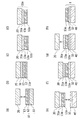
以下、本発明に係るデバイス基板及びその製造方法の一実施形態について説明するが、本発明の範囲は、この形態に限定されるものではない。本実施の形態のデバイス基板の製造方法は、SOIデバイス基板を支持基板に仮接合用接着剤で仮接合する仮接合工程と、この仮接合したSOIデバイス基板からSiベース基板を除去するSiベース基板除去工程と、Siベース基板を除去した部分に、転写基板を転写用接着剤で転写接合する転写接合工程と、支持基板を剥離する剥離工程と、残存する仮接合用接着剤を除去する接着剤除去工程とから主に構成されている。各構成物、及び各工程について添付図面の図1を参照して、詳細に説明する。 Hereinafter, an embodiment of the device substrate and the method for manufacturing the device substrate according to the present invention will be described, but the scope of the present invention is not limited to this embodiment. The device substrate manufacturing method of the present embodiment includes a temporary bonding step of temporarily joining the SOI device substrate to the support substrate with a temporary bonding adhesive, and a Si base substrate that removes the Si base substrate from the temporarily bonded SOI device substrate. A removal step, a transfer bonding step of transferring and joining the transfer substrate to the portion from which the Si base substrate has been removed with a transfer adhesive, a peeling step of peeling off the support substrate, and an adhesive for removing the remaining temporary bonding adhesive. It mainly consists of a removal process. Each component and each process will be described in detail with reference to FIG. 1 of the accompanying drawing.
1.仮接合工程
仮接合工程について説明する。デバイスを形成したSOIデバイス基板10と支持基板20とを仮接合用接着剤31を用いて接合する(図1(a))。SOIデバイス基板10は、Siベース基板11と、Siベース基板11上に形成したBox層(埋め込み酸化膜層)12と、Box層12上に形成したSiデバイス層13とからなる。1. 1. Temporary joining process The temporary joining process will be described. The
SOIデバイス基板10は、高性能プロセッサーや高周波デバイスなどに一般的に使用されるSOIデバイス基板と同様の構成および材料のものを用いることができる。Siベース基板11の厚さは、200μm以上が好ましく、300μm以上がより好ましい。Siベース基板11の厚さを200μm以上とすることで、ウエハーの撓みを生じず搬送することができる。厚さの上限は特に限定されないが、後述する切削、研磨、エッチング等を容易にするため、1000μm以下にすることが好ましい。
As the
Box層12は、少なくともSiO2より高い熱伝導率を有し且つ電気絶縁体である。具体的には、熱伝導率は1.5W/m・Kより高いことが好ましく、10W/m・K以上がより好ましく、100W/m・K以上がさらに好ましい。このような材料として、AlN、Si3N4、Al2O3、ダイヤモンド等がある。The
Box層12の厚さは、50〜10000nmの範囲が好ましく、500nm以下の範囲がより好ましい。厚さが50nm以上であることにより、Siベース基板の影響を受けにくくし、Siベース基板の除去時にデバイス層まで影響を及ぼさず加工する事ができる。厚さが10000nmを以下であることにより、接合応力が小さくなり、反りにくくなる。
The thickness of the
Siデバイス層13は、厚さは通常4〜10μmであるが、設置する配線数により、適宜変更可能である。厚さが4μm以上であることにより多層配線にすることができ、10μm以下であることにより必要な配線数を確保できる。Siデバイス層13の厚さは、4〜8μmの範囲がより好ましい。また、Siデバイス層13の表面には半田バンプが形成されていてもよい。
The thickness of the
支持基板20は、使用する仮接合用接着剤31の硬化方法にもよるが、Siと同程度の線膨張係数の基板を用いることが望ましい。具体的には、線膨張係数は5.0×10⁻⁶/℃以下が好ましい。線膨張係数が5.0×10−6/℃より大きいと、仮接合する際に熱がかかる場合、Siデバイス層13のシリコンとの熱膨張係数の差が大きいため、基板全体が反ったりするおそれがある。このような材料としては、Siウェハ、テンパックス、EAGLE−XGなどを用いる事が出来る。Although the
仮接合用接着剤31は、接着させた2層が剥離可能な接着剤であれば特に限定されないが、例えば、アクリルや、シリコーン、エポキシ、ホットメルト等の接着剤を用いることができる。仮接合用接着剤31としては、具体的には、3M社製のWSS(UV硬化アクリル系接着剤)や信越化学社製のTA1070T/TA2570V3/TA4070など熱硬化性変性シリコーンを主成分とする接着剤を用いることができる。特に、裏面エッチング時の酸/アルカリ耐性が優れた後者の熱硬化性変性シリコーンを主成分とする接着剤を仮接合用接着剤として用いる事が特に好ましい。酸耐性に優れた接着剤としては、その他に、フッ素系樹脂などもある。
The
また、接着させた2層の剥離を容易にできるように、支持基板20上に異なる仮接合用接着剤31の複数の層を形成してもよい。仮接合用接着剤31の厚さは、特に限定されないが、10〜200μmの範囲が好ましい。
Further, a plurality of layers of different
2.Siベース基板除去工程
Siベース基板除去工程について説明する。Siベース基板除去工程は、Siベース基板11を薄化する薄化工程と、支持基板20に仮接合したSOIデバイス基板10及び仮接合用接着剤31の外周部をトリミングするエッジトリミング工程と、これら工程によって残ったSiベース基板11をエッチングで除去するエッチング工程とを更に含むことが好ましい。2. Si base substrate removing step The Si base substrate removing step will be described. The Si base substrate removing step includes a thinning step of thinning the
Siベース基板除去工程の薄化工程について説明する。仮接合工程の後、SOIデバイス基板10のSiベース基板11を薄くする(図1(b))。薄化の方法としては、研削、研磨、エッチング等があるが、必要に応じて適宜変更してもよい。スループットの観点から研削によって薄化することが好ましく、例えば、#600〜#2000の砥石を組み合わせて加工することにより薄化することが更に好ましい。また、必要に応じて研削後に、例えばCMPやドライポリッシュなどを行い平滑化してもよい。
The thinning step of the Si base substrate removing step will be described. After the temporary joining step, the
加工歪みをSiデバイス層13まで及ぼさないように、Siベース基板11を10〜100μm残すことが好ましく、残す厚さは、20μm以上、50μm以下がより好ましい。薄化したSiベース基板11aが10μm以上であることにより、加工歪みがSiデバイス層13に及びにくくなり、また、100μm以下であることにより、その後のエッチングによって、薄化したSiベース基板11aを除去するエッチング時間を短くできる。
It is preferable to leave the
次に、Siベース基板除去工程のエッジトリミング工程について説明する。Siベース基板11を薄化工程にて十分に薄化した後、エッジトリミングを行う(図1(c))。SOIデバイス基板10の外周部においては、その面内中央部に比べ仮接合用接着剤31の層が厚くなる傾向がある。そこで、仮接合用接着剤31の厚さが均一な部分を残すべく、SOIデバイス基板10及び仮接合用接着剤31の外周部を除去する。エッジトリミング量は、仮接合用接着剤31の残渣を十分に除去でき、且つ、デバイス部分の面積を減らさないように、適宜決定することができる。具体的には、SOIデバイス基板10の縁(エッジ)から面内中央部に向かって2〜5mmの部分までを、仮接合用接着剤31とともに除去する。なお、支持基板20には仮接合用接着剤31が塗布されていないため、エッジトリミングを行わなくてよい。
Next, the edge trimming step of the Si base substrate removing step will be described. After the
エッジトリミングの方法としては、グラインダーによる研削、研磨フイルムを用いたテープ研磨等がある。好ましくはテープ研磨である。グラインダーによる研削を行うと、仮接合用接着剤31に変性シリコーンを用いる場合、樹脂が柔らかいため砥石が目詰まりを起こし、焼きつきや基板の剥がれが発生する。一方でテープ研磨にてエッジトリミングを実施することにより、支持基板20からSiデバイス層13の剥がれや割れ等が生じず良好なトリミングが可能となる。
Examples of the edge trimming method include grinding with a grinder and tape polishing using a polishing film. Tape polishing is preferable. When grinding with a grinder is performed, when modified silicone is used as the
次に、Siベース基板除去工程のエッチング工程について説明する。エッジトリミング工程に続いて、残ったSiベース基板11bを完全除去するためのエッチングを行い、薄化デバイスウェハ10aを得る(図1(d))。エッチングは酸またはアルカリによって実施可能であるが、エッチング速度の観点によると、酸によるエッチングが好ましい。KOHやNH4OHのアルカリによるエッチングでは20μmのSiベース基板11bをエッチングするのに70℃で1時間以上かかるのに対し、酸によるエッチングでは室温において数分でエッチングすることが可能だからである。用いる酸としては、HF、HNO3、CH3COOH、H2SO4、H3PO4などの強酸を任意に選択・混合した酸がより好ましい。なお、Siベース基板11bを完全除去するに際し、従来用いられている研削やCMPによる薄化は、加工痕が残存するため好ましくない。また、酸によるエッチングでは、エッチングレートの速さの点で、ウェットエッチングがさらに好ましい。このようにSiベース基板11bを完全除去することにより、高周波領域での損失をより低減することができる。Next, the etching step of the Si base substrate removing step will be described. Following the edge trimming step, etching for completely removing the remaining
さらに、エッチングは浸漬や片面のスピンエッチングによって実施されるが、支持基板20のエッチングを抑制する観点で、片面のスピンエッチングが好ましい。SOIデバイス基板10の外周部ではエッジトリミングを行ったことにより仮接合用接着剤31aの層が露出されている。使用する仮接合用接着剤31が酸に対する耐性が無い場合、仮接合用接着剤31がSOIデバイス基板10の外周部からエッチング液で侵食されることによりSiデバイス層13の外周部分から皺が入り剥がれが発生する。例えば、酸に対する耐性がない3M社製のWSS(UV硬化アクリル系接着剤)を仮接合用接着剤31として用いた場合、酸による浸食があり、SOIデバイス基板10の外周部から剥がれが発生し、本発明への使用には適さない。これに対し、酸に対する耐性がある変性シリコーン系の接着剤を仮接合用接着剤31として用いた場合には剥がれは生じず、高熱伝導で且つ電気絶縁体の薄膜Box層12が露出するまでエッチングすることが可能である。この工程で得られるSiベース基板11bが完全に除去された基板を薄化デバイスウェハ10aという。
Further, although the etching is carried out by immersion or spin etching on one side, spin etching on one side is preferable from the viewpoint of suppressing etching of the
3.転写接合工程
転写接合工程について説明する。電気絶縁体である転写基板40側に転写用接着剤32を塗布し(図1(e))、薄化デバイスウェハ10aと接合する(図1(f))。3. 3. Transfer bonding step The transfer bonding process will be described. The
転写基板40は、200〜300mmφのウェハサイズが得られるものが好ましい。また、サファイヤ、アルミナ、AlN焼結体、Si3N4焼結体、ダイヤモンドなどを用いることが好ましい。これらは、SiO2よりも高い熱伝導率を有し且つ電気絶縁体であり、さらに、一般的には高価な単結晶よりも、コストの点から好適だからである。具体的には、熱伝導率は1.5W/m・Kより高いことが好ましく、10W/m・K以上がより好ましく、100W/m・K以上がさらに好ましい。The
転写用接着剤32は、Siデバイス層13形成後のプロセス温度から150℃に耐性があり、好ましくは250℃の温度に耐性があり、より好ましくは300℃の温度に耐性があり、且つ転写接合時にSiデバイス層13への応力を小さくするため、シリコーン樹脂、エポキシ変性ゴム、エポキシ変性シリコーンなどを用いることが好ましい。特にエポキシ変性シリコーンは接着剤は強度も強く、硬化時の熱応力が小さく、又、薄く形成することができ、且つ接着力を保持する点から最も好ましい。具体的には、信越化学社製のTA1070T、TA2570V3、TA4070などの熱硬化性変性シリコーンが好ましい。
The
転写用接着剤32の層の厚さは、0.1〜5μmが好ましい。より好ましくは0.1μm以上、2μm以下である。更に好ましくは、0.1μm以上、1μm以下である。転写用接着剤32の層の厚さが5μmを超えると、放熱性は転写用接着剤32無しの場合に比べ1/2以下になるため、熱伝導度を高めるために5μm以下で設けることが好ましい。また0.1μm以上であることによって十分な接合強度を維持し、面内均一に塗布し接合しやすくなる。
The thickness of the layer of the
また、転写用接着剤32の熱伝導率は1W/m・K程度と小さいため、熱伝導率の高い基板を作製するためには、なるべく薄く且つ均一に転写用接着剤32の層を形成することが好ましい。
Further, since the thermal conductivity of the
なお、転写基板40とBox層12aとの接合面には、転写用接着剤32を塗布する前に、SiO2、Si3N4、オキシナイトライド(SiOxNy)からなる群から選ばれるいずれか1種またはこれらの組み合わせから成る薄膜を形成してもよい。このような薄膜を形成することで、表面粗さや濡れ性を改善し、接合力を向上することができる。この薄膜の厚さは、0.05〜10μmの範囲が好ましい。製膜法は、特に限定されないが、例えば、プラズマ製膜法や化学的気相成長法、物理的気相成長法等が好ましい。この薄膜は、転写基板40上に形成することに代えて又は加えて、薄化デバイスウェア10aのBox層12a表面に形成してもよい。Before applying the
図1(e)に示すように、薄化デバイスウェハ10aの表面には、Box層12aが露出している。Box層12aは、通常、50〜1000nmであるが、Siベース基板11bが完全に除去されると、Siデバイス層13のパターン配線による局所的な応力によりBox層12aが局所的に変形し、配線パターンに対応して高さ1〜10nmの段差が発生する。こうした段差があると、直接接合やプラズマ接合では転写基板40と接合することができない。そこで、段差のある面を転写基板40に接合すべく、転写用接着剤32を介して接合を行う。
As shown in FIG. 1 (e), the
転写用接着剤32を塗布すると、溶媒除去のため及び接合時の加温による脱ガスを防ぐために100〜200℃でベーキング及びハーフキュアをすることが好ましい。好ましくは120℃以上、180℃以下である。
When the
このとき、Box層12a側に転写用接着剤32を塗布してベーキングすると、仮接合用接着剤31aの成分が変形しラメラ状の凹凸やボイドが発生する場合がある。したがって、転写用接着剤32は転写基板40側に塗布することが好ましい。
At this time, when the
転写用接着剤32を塗布する方法としては、ダイコート、スリットコート、デイップコート、スピンコート等の方法を用いることができるが、接合面側にのみ均一に塗布できる点でスピンコートが好ましい。
As a method of applying the
図1(f)に示すように、Box層12aと転写用接着剤32を塗布した転写基板40とを接合する。例えば接合前の加温に続いて、薄化デバイスウェハ10aと転写用接着剤32を塗布した転写基板40とを接合面を対向させ荷重をかけ接触させる。その荷重を保持しつつ加温し、転写用接着剤32をフルキュアすることによって接合させる。印加する荷重の上限は、例えば20kgf/cm2未満、好ましくは10kgf/cm2以下、より好ましくは5kgf/cm2以下である。20kgf/cm2未満であることにより、Siデバイス層13、特に半田バンプの変形が生じない荷重で接合できる。また、1kgf/cm2以上の荷重をかけることが好ましい。1kgf/cm2以上であることによって、転写基板40自体が有する5〜50μmの反りを矯正しつつ重ね合わせられる。なお、基板の反りは、薄化デバイスウェハ10a及び転写基板40の双方が有しうるが、接合時に荷重を印加することでこの反りを矯正することができる。As shown in FIG. 1 (f), the
接合時に加温する温度は、転写用接着剤32の耐熱温度及び半田バンプの融点を超えない範囲で出来るだけ高い方が好ましい。特に、接合時に加温する温度は、使用する転写用接着剤32の耐熱温度及び半田バンプの融点のうち温度が低い方の温度よりも15〜50℃低いことがより好ましく、20〜40℃低いことが更に好ましい。例えば半田バンプの融点が250℃の場合、好ましくは200〜245℃、より好ましくは220〜240℃の温度範囲に昇温する。
The temperature to be heated at the time of joining is preferably as high as possible within a range not exceeding the heat resistant temperature of the
接合時に加温する温度範囲を保持する時間は、短い方がスループットの面で好ましい。保持時間は、1〜60分、好ましくは2〜30分、より好ましくは5〜10分である。 It is preferable that the time for maintaining the temperature range to be heated at the time of joining is short in terms of throughput. The holding time is 1 to 60 minutes, preferably 2 to 30 minutes, and more preferably 5 to 10 minutes.
転写接合は大気または真空いずれの雰囲気においても実施可能であるが、1E−1〜1E−5Torr、好ましくは1E−2〜1E−4Torrの真空下で接合を行うことが好ましい。1E−5Torr以上であることにより、接合界面の気泡が残存しないように転写接合できる。Transcription bonding can also be carried out in any atmosphere or vacuum atmosphere, 1E -1 ~1E -5 Torr, preferably it is preferable to perform the bonding under a vacuum of 1E -2 ~1E -4 Torr. When it is 1E- 5 Torr or more, transfer bonding can be performed so that bubbles at the bonding interface do not remain.
転写接合工程は、Siデバイス層13aを反転しないで転写する方法であるため、Siデバイス層13aに半田バンプまで形成した状態で転写することが可能であり、転写後に電気配線形成等の能動部を形成するプロセスは不要となる。
Since the transfer bonding step is a method of transferring the
4.剥離工程
剥離工程について説明する。仮接合していた支持基板20を剥離する(図1(g))。剥離工程は通常、物理的(機械的手段を含む)、又は化学的な手段を単独又は組み合わせて行うことができる。例えば、支持基板20は、機械的な力、例えば接合面の一端に楔を挿入する事で支持基板20を外し、剥離が容易に行える。また、化学的な手段としては、例えば、溶媒による膨潤、溶解などを利用することができる。また、光化学的な手段として光硬化などを利用することができる。4. Peeling step The peeling step will be described. The temporarily joined
5.接着剤除去工程
接着剤除去工程について説明する(図1(h))。必要に応じて、Siデバイス層13aの表面に残った仮接合用接着剤31aの残渣を洗浄する、接着剤除去工程を行うことができる。仮接合用接着剤31は有機溶媒、例えばp−メンタンにより膨潤するため、Siデバイス層13aをp−メンタンに浸漬させることで容易に仮接合用接着剤31aの残渣を除去することができる。浸漬する時間は1〜10分、好ましくは3〜5分である。5. Adhesive Removal Step An adhesive removal step will be described (FIG. 1 (h)). If necessary, an adhesive removing step of cleaning the residue of the temporary bonding adhesive 31a remaining on the surface of the
以上、説明する本実施の形態のデバイス基板の製造方法により、Siデバイス層13aと、Box層12aと、転写用接着剤32を介して、転写基板40が積層されたデバイス基板1を得ることができる。上述してきたように本実施の形態のデバイス基板の製造方法では金属不純物の拡散が生じる高温プロセスを必要としない。また、Box層12aおよび転写基板40は、高熱伝導で且つ電気絶縁体であることから、放熱性に優れ、且つ高周波に対する損失が小さい。さらに、薄化デバイスウェハ10aを得る際に、上述したようにSOIデバイス基板10のSiベース基板11を除去するために適した所定の条件で実施したことから、支持基板20からの剥がれが発生することもない。
By the device substrate manufacturing method of the present embodiment described above, it is possible to obtain the
以下に実施例および比較例を挙げて、本発明をより具体的に説明するが、本発明はこれに限定されるものではない。 Hereinafter, the present invention will be described in more detail with reference to Examples and Comparative Examples, but the present invention is not limited thereto.
[実施例1]
デバイスを形成したSOIデバイス基板として、外形300mmφ、厚さ4μmのSiデバイス層と、AlNを用いた厚さ250nmの薄膜Box層と、厚さ725μmのSiベース基板からなるウェハを用いた。デバイス最表面には、直径80μmの半田バンプを、最小ピッチ150μmで形成した。[Example 1]
As the SOI device substrate on which the device was formed, a wafer composed of a Si device layer having an outer diameter of 300 mmφ and a thickness of 4 μm, a thin film Box layer having a thickness of 250 nm using AlN, and a Si base substrate having a thickness of 725 μm was used. On the outermost surface of the device, solder bumps having a diameter of 80 μm were formed with a minimum pitch of 150 μm.
このSOIデバイス基板のSiデバイス層が設けられた面に仮接合用接着剤として信越化学社製のシリコーン樹脂の接着剤、TA1070T/TA2570V3/TA4070をスピンコートにより積層塗布した。すなわち、まずデバイス保護層としてTA1070Tを10μm、加工後に支持基板の剥離面となる層としてTA2570V3を10μm、支持基板との接着層としてTA4070を100μm積層した。支持基板としてSiウェハを用い、仮接合用接着剤と支持基板とをEV Group社製の半自動ウェハボンダEVG520ISを用い、10−4Torrの真空下、1kgf/cm2の荷重をかけ140℃で保持し接合し、その後190℃で2時間オーブンで処理し仮接合用接着剤を硬化させた。TA1070T / TA2570V3 / TA4070, a silicone resin adhesive manufactured by Shin-Etsu Chemical Co., Ltd., was laminated and coated on the surface of the SOI device substrate provided with the Si device layer as a temporary bonding adhesive. That is, first, TA1070T was laminated by 10 μm as a device protective layer, TA2570V3 was laminated by 10 μm as a layer to be a peeling surface of the support substrate after processing, and TA4070 was laminated by 100 μm as an adhesive layer with the support substrate. A Si wafer is used as the support substrate, and the temporary bonding adhesive and the support substrate are held at 140 ° C. by applying a load of 1 kgf / cm 2 under a vacuum of 10-4 Torr using a semi-automatic wafer bonder EVG520IS manufactured by EV Group. The bonding was then performed at 190 ° C. for 2 hours in an oven to cure the temporary bonding adhesive.
次に東京精密社製のポリッシュ・グラインダPG300を用い、♯2000の砥石で、SOIデバイス基板の裏面に位置するSiベース基板を厚さ40μmまで薄化した。研削後の表面にはソーマークは観察されるものの、ウェハの剥がれや割れ、エッジチップは見られなかった。 Next, using a polish grinder PG300 manufactured by Tokyo Seimitsu Co., Ltd., the Si base substrate located on the back surface of the SOI device substrate was thinned to a thickness of 40 μm with a # 2000 grindstone. Although saw marks were observed on the surface after grinding, no peeling or cracking of the wafer or edge chips were observed.
続いて、MIPOX社製のウェハエッジ研磨装置NME−123Nを用いテープ研磨にてエッジトリミングを実施した。トリミング幅はウェハ最外周から2mm内側までとした。割れや剥がれを生じずトリミングする事ができた。 Subsequently, edge trimming was performed by tape polishing using a wafer edge polishing device NME-123N manufactured by MIPOX. The trimming width was set to 2 mm inside from the outermost circumference of the wafer. It was possible to trim without cracking or peeling.
続いて、三益半導体社製のスピンエッチャーMSE2000を用い、酸によるスピンエッチングによって裏面側に残存する40μmの厚さのSiベース基板を除去した。使用した酸はHF/HNO3/H3PO4/H2SO4の混酸であり、3分のエッチング時間でSiベース基板を完全に除去して薄化デバイスウェハを得た。Subsequently, using a spin etcher MSE2000 manufactured by Sanmasu Semiconductor Co., Ltd., a 40 μm-thick Si base substrate remaining on the back surface side was removed by spin etching with an acid. The acid used was a mixed acid of HF / HNO 3 / H 3 PO 4 / H 2 SO 4 , and the Si base substrate was completely removed in an etching time of 3 minutes to obtain a thin device wafer.
次に、高熱伝導で且つ電気絶縁体の転写基板として、外径300mmφ、厚さ725μm、熱伝導率200W/m・K、抵抗率5E+15Ω・cmのAlN焼結体基板を用いた。転写用接着剤として、低応力の熱硬化性エポキシ変性シリコーン接着剤であるTA4070をシクロペンタノンで希釈し、接着剤濃度が0.5wt%の塗布液を調製した。これを転写基板として準備したAlNウェハにスピンコートすることで厚さ1μmの転写用接着剤の層を面内ばらつき±5%で形成した。転写用接着剤を塗布した転写基板を、150℃で5分ベーキングし、溶媒除去とハーフキュアを行った。Next, as a transfer substrate having high thermal conductivity and an electrical insulator, an AlN sintered substrate having an outer diameter of 300 mmφ, a thickness of 725 μm, a thermal conductivity of 200 W / m · K, and a resistivity of 5E + 15 Ω · cm was used. As the transfer adhesive, TA4070, which is a low-stress thermosetting epoxy-modified silicone adhesive, was diluted with cyclopentanone to prepare a coating liquid having an adhesive concentration of 0.5 wt%. By spin-coating this on an AlN wafer prepared as a transfer substrate, a layer of a transfer adhesive having a thickness of 1 μm was formed with an in-plane variation of ± 5%. The transfer substrate coated with the transfer adhesive was baked at 150 ° C. for 5 minutes to remove the solvent and half-cure.
続いて、SussMicroTec社製のウェハボンダーSB8を用いて薄化デバイスウェハと転写基板とを接合した。転写用接着剤を塗布した転写基板と薄化デバイスウェハを室温下で重ね合わせ、3kgf/cm2の荷重をかけ、1E−4Torrの真空下240℃で10分保持することにより接合した。その後、65℃以下の温度で荷重を外し、接合済みのウェハを取り出した。Subsequently, the thinning device wafer and the transfer substrate were joined using a wafer bonder SB8 manufactured by SussMicroTech. The transfer substrate coated with the transfer adhesive and the thinning device wafer were superposed at room temperature, loaded with a load of 3 kgf / cm 2 , and held at 240 ° C. under a vacuum of 1E-4 Torr for 10 minutes to bond them. Then, the load was removed at a temperature of 65 ° C. or lower, and the bonded wafer was taken out.
接合済みのウェハの仮接合界面に楔を入れて機械的に支持基板を剥がすことにより、Box層を介して転写基板にSiデバイス層を転写することができた。外観上、転写したSiデバイス層の剥がれは無かった。また、光学顕微鏡で面内のデバイスパターンを観察したところ、パターンの割れは無く、半田バンプの剥がれも認められなかった。 The Si device layer could be transferred to the transfer substrate via the Box layer by inserting a wedge into the temporary bonding interface of the bonded wafer and mechanically peeling off the support substrate. Apparently, the transferred Si device layer was not peeled off. Further, when the in-plane device pattern was observed with an optical microscope, the pattern was not cracked and the solder bumps were not peeled off.
Siデバイス層を転写したBox層をp−メンタンに5分間浸漬することにより、表面に残存した仮接合用接着剤を除去した。転写したSiデバイス層とBox層との界面に剥がれは見られず、転写用接着剤がp−メンタンにより溶出することは無かった。洗浄後のデバイス表面を光学顕微鏡にて観察したところ、パターンの割れや半田バンプの変形は認められなかった。このように、元のデバイスパターン形状を保った状態でSiデバイス層をBox層に転写する事ができた。この転写基板から個別のデバイスを分割後、1GHzの高周波を印加し、1時間後にデバイスの表面温度を測定したところ、殆ど温度上昇が見られなかった。又、信号とノイズのアイソレーションは極めて高く、良好であった。 The Box layer to which the Si device layer was transferred was immersed in p-menthane for 5 minutes to remove the temporary bonding adhesive remaining on the surface. No peeling was observed at the interface between the transferred Si device layer and the Box layer, and the transfer adhesive was not eluted by p-menthane. When the surface of the device after cleaning was observed with an optical microscope, no cracks in the pattern or deformation of the solder bumps were observed. In this way, the Si device layer could be transferred to the Box layer while maintaining the original device pattern shape. After dividing each device from this transfer substrate, a high frequency of 1 GHz was applied, and the surface temperature of the device was measured 1 hour later. As a result, almost no temperature rise was observed. Moreover, the isolation between the signal and the noise was extremely high and good.
[実施例2]
Box層が、メタン、水素の混合ガスから合成した高熱伝導で且つ電気絶縁体のダイヤモンドで、その厚さが200nmのものを用いた他は実施例1と同じSOIデバイス基板を準備し、実施例1と同様の手順で、薄化デバイスウェハを経てデバイス基板を作製した。但し、転写基板としてAlN基板の代わりにSi3N4基板を用い、転写用接着剤の塗布も同様の手順にて実施したが、接合時の荷重を1kgf/cm2に下げて実施した。[Example 2]
The same SOI device substrate as in Example 1 was prepared except that the Box layer was a diamond having a high thermal conductivity and an electrical insulator synthesized from a mixed gas of methane and hydrogen and having a thickness of 200 nm. A device substrate was produced through the thinned device wafer in the same procedure as in 1. However, a Si 3 N 4 substrate was used as the transfer substrate instead of the Al N substrate, and the transfer adhesive was applied in the same procedure, but the load at the time of joining was reduced to 1 kgf / cm 2.
薄化デバイスウェハは均一に接合していた。支持基板を剥離したところ、Siデバイス層をBox層を介して転写基板に転写することができた。洗浄後のSiデバイス層を光学顕微鏡で観察したが、剥がれやバンプの変形は見られなかった。この転写基板を実施例1と同一の条件で温度上昇を測定したところ、測定前から約3℃上昇したがその後それ以上の温度上昇は見られず、略一定で安定していた。又、アイソレーションは良好であった。 The thinning device wafers were uniformly bonded. When the support substrate was peeled off, the Si device layer could be transferred to the transfer substrate via the Box layer. The Si device layer after cleaning was observed with an optical microscope, and no peeling or deformation of bumps was observed. When the temperature rise of this transfer substrate was measured under the same conditions as in Example 1, the temperature rose by about 3 ° C. from before the measurement, but no further temperature rise was observed thereafter, and the temperature rise was substantially constant and stable. Also, the isolation was good.
[実施例3]
SOIデバイス基板のBox層がスパッター法で付けた高熱伝導で且つ電気絶縁体のAl2O3で、膜厚が150nmとした他は、実施例1と同じく形成したSOIデバイス基板を準備し、実施例1と同様の手順で、薄化デバイスウェハを経てデバイス基板を作製した。なお、Box層への転写用接着剤の塗布も同様の手順にて実施したが、接合時の荷重を10kgf/cm2に上げて実施した。[Example 3]
The SOI device substrate formed in the same manner as in Example 1 was prepared and carried out, except that the Box layer of the SOI device substrate was Al 2 O 3 which is a high thermal conductivity and an electrical insulator attached by a sputtering method and had a film thickness of 150 nm. A device substrate was produced through the thinned device wafer in the same procedure as in Example 1. The transfer adhesive was applied to the Box layer in the same procedure, but the load at the time of joining was increased to 10 kgf / cm 2.
薄化デバイスウェハは良く接合されていた。支持基板を剥離したところ、Siデバイス層をBox層を介して転写基板に転写する事ができた。洗浄後のSiデバイス層を光学顕微鏡で観察したが、剥がれやバンプの変形は見られなかった。実施例1と同一条件下にて温度上昇を測定した結果、約5℃の上昇が見られたがそれ以上には上がらなかった。又、アイソレーションも優れていた。 The thinning device wafers were well bonded. When the support substrate was peeled off, the Si device layer could be transferred to the transfer substrate via the Box layer. The Si device layer after cleaning was observed with an optical microscope, and no peeling or deformation of bumps was observed. As a result of measuring the temperature rise under the same conditions as in Example 1, a rise of about 5 ° C. was observed, but the temperature rise did not rise any more. Also, the isolation was excellent.
[実施例4]
実施例1に記載のSOIデバイス基板を準備し、実施例1と同様の手順で、薄化デバイスウェハを経てデバイス基板を作製した。但し、転写基板としてAlN基板の代わりにSi3N4基板を用い、Box層との接合面には事前にSiO2を約1μmプラズマ成膜法で付けた後、研磨してRa0.5nm迄に平滑にした。その後、転写用接着剤の塗布も実施例1と同様の手順にて実施したが、接合時の温度を220℃に下げて実施した。[Example 4]
The SOI device substrate described in Example 1 was prepared, and a device substrate was produced via a thinned device wafer in the same procedure as in Example 1. However, a Si 3 N 4 substrate is used as the transfer substrate instead of the Al N substrate, and SiO 2 is previously attached to the bonding surface with the Box layer by a plasma film forming method of about 1 μm, and then polished to Ra 0.5 nm. Smoothed. After that, the transfer adhesive was applied in the same procedure as in Example 1, but the temperature at the time of joining was lowered to 220 ° C.
薄化デバイスウェハは接合されていた。支持基板を剥離したところ、Siデバイス層をBox層を介して転写基板に転写することができた。洗浄後のSiデバイス層を光学顕微鏡で観察したが、剥がれやバンプの変形は見られず、綺麗な状況を維持していた。実施例1と同様に温度上昇を測った結果、約7.5℃となり、以後は一定であった。又、アイソレーションは特に問題が無かった。 The thinning device wafers were joined. When the support substrate was peeled off, the Si device layer could be transferred to the transfer substrate via the Box layer. The Si device layer after cleaning was observed with an optical microscope, and no peeling or deformation of bumps was observed, and the condition was maintained in a clean state. As a result of measuring the temperature rise in the same manner as in Example 1, the temperature was about 7.5 ° C., which was constant thereafter. Moreover, there was no particular problem with isolation.
[実施例5]
実施例1に記載のSOIデバイス基板を準備し、実施例1と同様の手順で、薄化デバイスウェハを経てデバイス基板を作製した。但し、転写基板としてAlN基板の代わりにサファイヤ基板を用い、転写用接着剤の塗布では、接着剤濃度が0.05wt%の塗布液を調製し、塗布後の転写用接着剤の層厚を0.1μmとした。[Example 5]
The SOI device substrate described in Example 1 was prepared, and a device substrate was produced via a thinned device wafer in the same procedure as in Example 1. However, when a sapphire substrate is used as the transfer substrate instead of the AlN substrate and the transfer adhesive is applied, a coating liquid having an adhesive concentration of 0.05 wt% is prepared, and the layer thickness of the transfer adhesive after application is set to 0. It was set to 1 μm.
薄化デバイスウェハは接合さ・BR>黷トいた。支持基板を剥離したところ、外周から10mmの領域を除きSiデバイス層は転写されていた。大部分の転写はできていたことから、少なくとも0.1μm以上の厚さで転写用接着剤の層を設けることが面全体の転写に必要であることがわかった。実施例1と同一条件下で個別デバイスの温度上昇を測定した。約11℃の温度上昇が見られたがその後は一定であり、特に問題は生じなかった。又、アイソレーションは実用上では特に問題が無かった。
The thinning device wafer was joined. When the support substrate was peeled off, the Si device layer was transferred except for the
[比較例1]
通常のφ200mmのSOIデバイス基板であって、Siベース基板上に厚みが100nmのSiO2のBox層が形成され、実施例1と同様のSiデバイス層を形成したSOIデバイス基板を準備し、また、AlN焼結体の転写基板の代わりに合成石英の転写基板を用いた他は、実施例1と同様の手順にて、薄化デバイスウェハを経てデバイス基板を作製した。実施例1と同様に1GHzの高周波のデバイスとして使用したところ、デバイスの温度が60℃迄まで上昇し、ノイズ/信号のアイソレーションが著しく悪くなり、使用不能であった。[Comparative Example 1]
An SOI device substrate which is a normal φ200 mm SOI device substrate and has a SiO 2 Box layer having a thickness of 100 nm formed on the Si base substrate and has the same Si device layer as in Example 1 is prepared. A device substrate was produced via a thinning device wafer in the same procedure as in Example 1 except that a synthetic quartz transfer substrate was used instead of the transfer substrate of the AlN sintered body. When it was used as a high-frequency device of 1 GHz as in Example 1, the temperature of the device rose to 60 ° C., and the noise / signal isolation was significantly deteriorated, so that it could not be used.
[比較例2]
実施例1と同様のSOIデバイス基板を準備し、実施例1と同様の手順で、薄化デバイスウェハを経てデバイス基板を作製した。但し、転写用接着剤として、耐熱温度が120℃の液状エポキシ樹脂を用い、また、AlNからなる転写基板にではなく、薄化デバイスウェハ側にスピンコートにより塗布し、110℃でベークした。その結果、薄化デバイスウェハに雛が入り、支持基板から剥がれていた。すなわち、接合されておらず、薄化デバイスウェハの厚さが薄い状態では、仮接合用接着剤の熱による変形を抑制する事ができず、雛が入ってしまった。その上、転写用接着剤の耐熱温度が低い為、転写基板も半田耐熱に耐えられずに転写基板のデバイスは殆ど導通不良のデバイスとなった。[Comparative Example 2]
The same SOI device substrate as in Example 1 was prepared, and the device substrate was prepared through the thinned device wafer by the same procedure as in Example 1. However, as the transfer adhesive, a liquid epoxy resin having a heat resistant temperature of 120 ° C. was used, and the coating was applied to the thinning device wafer side by spin coating instead of the transfer substrate made of AlN, and baked at 110 ° C. As a result, chicks entered the thinning device wafer and peeled off from the support substrate. That is, when the thinning device wafer was not bonded and the thickness of the thinning device wafer was thin, the deformation of the temporary bonding adhesive due to heat could not be suppressed, and chicks were inserted. Moreover, since the heat-resistant temperature of the transfer adhesive is low, the transfer substrate cannot withstand the heat resistance of solder, and the device of the transfer substrate is almost a device with poor continuity.
[比較例3]
仮接合用接着剤として3M社製のWSSを用い、支持基板との仮接合を行った。WSSはアクリル系のUV硬化接着剤であり、YAGレーザーを照射し剥離する層を設けた構成である。そのため支持基板はUV〜近赤外で透明である必要があり、ここではテンパックス基板を支持基板に用いた。その他は、実施例1と同様の手順で、裏面を研削し、エッジトリミングを行い、酸によるエッチングを行った。トリミング後のデバイスウェハ外周部分が剥がれ、基板の中心に向かって雛が発生した。これはWSSに用いられる紫外線吸収層が酸により浸食され、支持基板から剥がれたためである。酸による浸食が確認されたため、アルカリである50%KOHを用い、70℃でスピンエッチングを試みたが、エッチング途中でデバイスウェハの外周部に剥がれが生じた。WSSでは薄化デバイスウェハと支持基との接合を保持した状態でウェハ裏面のSiベース基板を完全に除去することができなかった。[Comparative Example 3]
WSS manufactured by 3M Co., Ltd. was used as the adhesive for temporary bonding, and temporary bonding with the support substrate was performed. WSS is an acrylic UV-curable adhesive, and has a structure provided with a layer that irradiates a YAG laser to peel off. Therefore, the support substrate needs to be transparent in UV to near infrared, and here, the Tempax substrate is used as the support substrate. Other than that, the back surface was ground, edge trimming was performed, and etching with acid was performed in the same procedure as in Example 1. The outer peripheral portion of the device wafer after trimming was peeled off, and chicks were generated toward the center of the substrate. This is because the ultraviolet absorbing layer used for WSS was eroded by the acid and peeled off from the support substrate. Since erosion by acid was confirmed, spin etching was attempted at 70 ° C. using 50% KOH, which is an alkali, but peeling occurred on the outer peripheral portion of the device wafer during the etching. In WSS, the Si base substrate on the back surface of the wafer could not be completely removed while maintaining the bonding between the thinning device wafer and the support group.
尚、上記に本実施形態を説明したが、本発明はこれらの例に限定されるものではない。例えば、前述の各実施形態に対して、当業者が適宜、構成要素の追加、削除、設計変更を行ったものや、各実施形態の特徴を適宜組み合わせたものも、本発明の要旨を備えている限り、本発明の範囲に含有される。 Although the present embodiment has been described above, the present invention is not limited to these examples. For example, those skilled in the art appropriately adding, deleting, or changing the design of each of the above-described embodiments, or those that appropriately combine the features of each embodiment also have the gist of the present invention. As long as it is, it is included in the scope of the present invention.
1 デバイス基板
10 SOIデバイス基板
10a 薄化デバイスウェハ
11 Siベース基板
12 Box層
13 Siデバイス層
20 支持基板
31 仮接合用接着剤
32 転写用接着剤
40 転写基板 1
Claims (12)
前記Box層の一方の面に形成されたSiデバイス層と、
前記Box層の反対面に、耐熱温度が150℃以上である接着剤を介して形成された少なくともSiO2より高い熱伝導率を有し且つ電気絶縁体である基板と
を備えるデバイス基板。A Box layer that has at least a thermal conductivity higher than SiO 2 and is an electrical insulator,
The Si device layer formed on one surface of the Box layer and
A device substrate provided on the opposite surface of the Box layer with a substrate formed via an adhesive having a heat resistant temperature of 150 ° C. or higher and having a thermal conductivity higher than that of SiO 2 and being an electrical insulator.
前記仮接合した前記SOIデバイス基板の前記Siベース基板を、研削、研磨、及びエッチングからなる群から選ばれるいずれか1種またはこれらの組み合わせで、前記Box層が露出するまで除去して薄化デバイスウェハを得るSiベース基板除去工程と、
前記薄化デバイスウェハの前記Box層側と転写基板とを耐熱温度が150℃以上である転写用接着剤で、加熱、加圧することにより転写接合する転写接合工程と、
前記支持基板を前記Siデバイス層から剥離する剥離工程と
を含むデバイス基板の製造方法。An SOI device substrate including a Si base substrate, a Box layer formed on the Si base substrate, and a Si device layer formed on the Box layer is placed on a support substrate on the Si device layer side of the SOI device substrate. In the temporary joining process of temporarily joining with an adhesive for temporary joining,
A thinning device in which the Si base substrate of the temporarily bonded SOI device substrate is removed by any one selected from the group consisting of grinding, polishing, and etching, or a combination thereof, until the Box layer is exposed. Si base substrate removal process to obtain wafer,
A transfer bonding step of transferring and bonding the Box layer side of the thinning device wafer and the transfer substrate by heating and pressurizing with a transfer adhesive having a heat resistant temperature of 150 ° C. or higher.
A method for manufacturing a device substrate, which comprises a peeling step of peeling the support substrate from the Si device layer.
Applications Claiming Priority (3)
| Application Number | Priority Date | Filing Date | Title |
|---|---|---|---|
| JP2017138026 | 2017-07-14 | ||
| JP2017138026 | 2017-07-14 | ||
| PCT/JP2018/026068 WO2019013212A1 (en) | 2017-07-14 | 2018-07-10 | Highly heat conductive device substrate and method for producing same |
Publications (2)
| Publication Number | Publication Date |
|---|---|
| JPWO2019013212A1 JPWO2019013212A1 (en) | 2020-04-16 |
| JP6854895B2 true JP6854895B2 (en) | 2021-04-07 |
Family
ID=65002076
Family Applications (1)
| Application Number | Title | Priority Date | Filing Date |
|---|---|---|---|
| JP2019529733A Active JP6854895B2 (en) | 2017-07-14 | 2018-07-10 | Highly thermally conductive device substrate and its manufacturing method |
Country Status (8)
| Country | Link |
|---|---|
| US (1) | US11361969B2 (en) |
| EP (1) | EP3654366A4 (en) |
| JP (1) | JP6854895B2 (en) |
| KR (1) | KR102558905B1 (en) |
| CN (1) | CN110892506B (en) |
| SG (2) | SG10201913156WA (en) |
| TW (1) | TWI798236B (en) |
| WO (1) | WO2019013212A1 (en) |
Families Citing this family (5)
| Publication number | Priority date | Publication date | Assignee | Title |
|---|---|---|---|---|
| JP6431631B1 (en) | 2018-02-28 | 2018-11-28 | 株式会社フィルネックス | Manufacturing method of semiconductor device |
| WO2020174529A1 (en) * | 2019-02-25 | 2020-09-03 | 三菱電機株式会社 | Method for manufacturing semiconductor element |
| JP7041648B2 (en) * | 2019-07-17 | 2022-03-24 | 信越化学工業株式会社 | Manufacturing method of composite substrate |
| CN112930106B (en) * | 2021-01-22 | 2022-11-22 | 杭州唯灵医疗科技有限公司 | Flexible electronic device and assembling method thereof |
| CN117813674A (en) * | 2021-08-17 | 2024-04-02 | 信越半导体株式会社 | Temporarily bonded wafer and method of manufacturing the same |
Family Cites Families (22)
| Publication number | Priority date | Publication date | Assignee | Title |
|---|---|---|---|---|
| US20020134503A1 (en) * | 2001-03-20 | 2002-09-26 | Accucorp Technical Services, Inc. | Silicon wafers bonded to insulator substrates by low viscosity epoxy wicking |
| JP2004047975A (en) | 2002-05-17 | 2004-02-12 | Semiconductor Energy Lab Co Ltd | Method of transferring laminate and method of manufacturing semiconductor device |
| EP1363319B1 (en) | 2002-05-17 | 2009-01-07 | Semiconductor Energy Laboratory Co., Ltd. | Method of transferring an object and method of manufacturing a semiconductor device |
| JP2005129825A (en) * | 2003-10-27 | 2005-05-19 | Sumitomo Chemical Co Ltd | Manufacturing method of compound semiconductor substrate |
| WO2005065402A2 (en) * | 2003-12-29 | 2005-07-21 | Translucent Photonics, Inc. | Rare earth-oxides, rare earth-nitrides, rare earth-phosphides and ternary alloys with silicon |
| JP4389626B2 (en) | 2004-03-29 | 2009-12-24 | ソニー株式会社 | Manufacturing method of solid-state imaging device |
| JP2007266044A (en) * | 2006-03-27 | 2007-10-11 | New Japan Radio Co Ltd | Method of manufacturing semiconductor device |
| JP5368996B2 (en) * | 2006-12-26 | 2013-12-18 | ソイテック | Method for manufacturing a semiconductor on insulator structure |
| JP2008218814A (en) * | 2007-03-06 | 2008-09-18 | Sumitomo Electric Ind Ltd | Power module |
| WO2009107701A1 (en) * | 2008-02-26 | 2009-09-03 | 京セラ株式会社 | Wafer-supporting member, method for producing the same, and electrostatic chuck using the same |
| US8092628B2 (en) * | 2008-10-31 | 2012-01-10 | Brewer Science Inc. | Cyclic olefin compositions for temporary wafer bonding |
| US8440544B2 (en) * | 2010-10-06 | 2013-05-14 | International Business Machines Corporation | CMOS structure and method of manufacture |
| KR20140118984A (en) | 2011-11-04 | 2014-10-08 | 더 실라나 그룹 피티와이 리미티드 | Method of producing a silicon-on-insulator article |
| CN104040685B (en) | 2011-12-22 | 2016-11-02 | 信越化学工业株式会社 | Composite base plate |
| WO2013168707A1 (en) * | 2012-05-08 | 2013-11-14 | 信越化学工業株式会社 | Heat dissipation substrate and method for producing same |
| JP2014086665A (en) | 2012-10-26 | 2014-05-12 | Sumitomo Electric Ind Ltd | Group-iii nitride donor composite substrate and manufacturing method thereof, and group-iii nitride composite substrate and manufacturing method thereof |
| US9741603B2 (en) * | 2013-05-01 | 2017-08-22 | Shin-Etsu Chemical Co., Ltd. | Method for producing hybrid substrate, and hybrid substrate |
| FR3012604B1 (en) * | 2013-10-25 | 2017-03-03 | Auxitrol Sa | PRESSURE SENSOR COMPRISING A STRUCTURE FOR CONTROLLING AN ADHESIVE LAYER RESISTANT TO TEMPERATURE VARIATIONS |
| JP6208646B2 (en) | 2014-09-30 | 2017-10-04 | 信越化学工業株式会社 | Bonded substrate, manufacturing method thereof, and supporting substrate for bonding |
| CN104617195B (en) * | 2015-02-06 | 2017-10-17 | 扬州乾照光电有限公司 | A kind of near-infrared luminous diode and its production method |
| CN105140122B (en) * | 2015-08-10 | 2018-07-20 | 中国电子科技集团公司第五十五研究所 | A method of improving GaN HEMT device heat dissipation performances |
| EP3537472B1 (en) * | 2016-11-01 | 2022-11-23 | Shin-Etsu Chemical Co., Ltd. | Method for transferring device layer to transfer substrate |
-
2018
- 2018-07-10 US US16/626,154 patent/US11361969B2/en active Active
- 2018-07-10 CN CN201880046539.7A patent/CN110892506B/en active Active
- 2018-07-10 WO PCT/JP2018/026068 patent/WO2019013212A1/en unknown
- 2018-07-10 JP JP2019529733A patent/JP6854895B2/en active Active
- 2018-07-10 EP EP18832873.6A patent/EP3654366A4/en active Pending
- 2018-07-10 SG SG10201913156WA patent/SG10201913156WA/en unknown
- 2018-07-10 SG SG11201912503WA patent/SG11201912503WA/en unknown
- 2018-07-10 KR KR1020197037807A patent/KR102558905B1/en active IP Right Grant
- 2018-07-13 TW TW107124206A patent/TWI798236B/en active
Also Published As
| Publication number | Publication date |
|---|---|
| KR20200026822A (en) | 2020-03-11 |
| CN110892506B (en) | 2024-04-09 |
| SG11201912503WA (en) | 2020-01-30 |
| US11361969B2 (en) | 2022-06-14 |
| CN110892506A (en) | 2020-03-17 |
| KR102558905B1 (en) | 2023-07-21 |
| SG10201913156WA (en) | 2020-02-27 |
| EP3654366A4 (en) | 2021-04-14 |
| US20200227263A1 (en) | 2020-07-16 |
| EP3654366A1 (en) | 2020-05-20 |
| JPWO2019013212A1 (en) | 2020-04-16 |
| TW201908124A (en) | 2019-03-01 |
| WO2019013212A1 (en) | 2019-01-17 |
| TWI798236B (en) | 2023-04-11 |
Similar Documents
| Publication | Publication Date | Title |
|---|---|---|
| JP6715345B2 (en) | Method of transferring device layer to transfer substrate | |
| JP6854895B2 (en) | Highly thermally conductive device substrate and its manufacturing method | |
| US20230187264A1 (en) | Methods for bonding semiconductor elements | |
| TW202343661A (en) | Dbi to si bonding for simplified handle wafer | |
| JP5095394B2 (en) | Wafer moving method | |
| KR20120052160A (en) | Composite substrate and composite substrate manufacturing method | |
| JP3502036B2 (en) | Semiconductor device manufacturing method and semiconductor device | |
| JP2011181919A (en) | Process for fabricating a multilayer structure with trimming using thermo-mechanical effects | |
| JP2012064710A (en) | Manufacturing method of semiconductor element | |
| CN108242393B (en) | Method for manufacturing semiconductor device | |
| JP2015508234A (en) | Method for three-dimensional mounting of electronic devices | |
| US20130154049A1 (en) | Integrated Circuits on Ceramic Wafers Using Layer Transfer Technology | |
| KR20200138320A (en) | Layer transfer method | |
| JP2010042469A (en) | Support plate | |
| CN113841223B (en) | Method for manufacturing semiconductor substrate and method for manufacturing semiconductor device | |
| CN109411359B (en) | Method and apparatus for processing semiconductor device structures | |
| WO2021210047A1 (en) | Method for manufacturing semiconductor element | |
| WO2020008882A1 (en) | Device-layer-transferred substrate production method and device layer-transferred substrate | |
| KR20200090812A (en) | Method for manufacturing residue of donor substrate, substrate produced by the method and use of the substrate | |
| KR19990055124A (en) | Double Silicon Substrate Manufacturing Method | |
| JP2013065760A (en) | Supporting substrate, method of manufacturing supporting substrate, and method of processing semiconductor substrate |
Legal Events
| Date | Code | Title | Description |
|---|---|---|---|
| A621 | Written request for application examination |
Free format text: JAPANESE INTERMEDIATE CODE: A621 Effective date: 20191219 |
|
| TRDD | Decision of grant or rejection written | ||
| A01 | Written decision to grant a patent or to grant a registration (utility model) |
Free format text: JAPANESE INTERMEDIATE CODE: A01 Effective date: 20210218 |
|
| A61 | First payment of annual fees (during grant procedure) |
Free format text: JAPANESE INTERMEDIATE CODE: A61 Effective date: 20210316 |
|
| R150 | Certificate of patent or registration of utility model |
Ref document number: 6854895 Country of ref document: JP Free format text: JAPANESE INTERMEDIATE CODE: R150 |