JP6851202B2 - Board holder, vertical board transfer device and board processing device - Google Patents
Board holder, vertical board transfer device and board processing device Download PDFInfo
- Publication number
- JP6851202B2 JP6851202B2 JP2017003338A JP2017003338A JP6851202B2 JP 6851202 B2 JP6851202 B2 JP 6851202B2 JP 2017003338 A JP2017003338 A JP 2017003338A JP 2017003338 A JP2017003338 A JP 2017003338A JP 6851202 B2 JP6851202 B2 JP 6851202B2
- Authority
- JP
- Japan
- Prior art keywords
- substrate
- chuck
- film
- holder
- board
- Prior art date
- Legal status (The legal status is an assumption and is not a legal conclusion. Google has not performed a legal analysis and makes no representation as to the accuracy of the status listed.)
- Active
Links
- 238000012546 transfer Methods 0.000 title claims description 44
- 238000012545 processing Methods 0.000 title claims description 17
- 239000000758 substrate Substances 0.000 claims description 229
- 230000002093 peripheral effect Effects 0.000 claims description 32
- 230000032258 transport Effects 0.000 claims description 28
- 238000004544 sputter deposition Methods 0.000 description 22
- 230000007246 mechanism Effects 0.000 description 9
- 238000000034 method Methods 0.000 description 7
- 238000001179 sorption measurement Methods 0.000 description 7
- 238000010438 heat treatment Methods 0.000 description 5
- 239000002245 particle Substances 0.000 description 5
- 230000008569 process Effects 0.000 description 3
- 238000005452 bending Methods 0.000 description 2
- 230000015572 biosynthetic process Effects 0.000 description 2
- 238000004891 communication Methods 0.000 description 2
- 230000007423 decrease Effects 0.000 description 2
- 238000000151 deposition Methods 0.000 description 2
- 230000008021 deposition Effects 0.000 description 2
- 239000011521 glass Substances 0.000 description 2
- 230000004048 modification Effects 0.000 description 2
- 238000012986 modification Methods 0.000 description 2
- 229910000838 Al alloy Inorganic materials 0.000 description 1
- HBBGRARXTFLTSG-UHFFFAOYSA-N Lithium ion Chemical compound [Li+] HBBGRARXTFLTSG-UHFFFAOYSA-N 0.000 description 1
- 230000008901 benefit Effects 0.000 description 1
- 229920002457 flexible plastic Polymers 0.000 description 1
- 230000006870 function Effects 0.000 description 1
- 238000009434 installation Methods 0.000 description 1
- 229910001416 lithium ion Inorganic materials 0.000 description 1
- 239000000463 material Substances 0.000 description 1
- 239000007769 metal material Substances 0.000 description 1
- 239000002985 plastic film Substances 0.000 description 1
- 239000010935 stainless steel Substances 0.000 description 1
- 229910001220 stainless steel Inorganic materials 0.000 description 1
- 238000004148 unit process Methods 0.000 description 1
Images


Classifications
-
- C—CHEMISTRY; METALLURGY
- C23—COATING METALLIC MATERIAL; COATING MATERIAL WITH METALLIC MATERIAL; CHEMICAL SURFACE TREATMENT; DIFFUSION TREATMENT OF METALLIC MATERIAL; COATING BY VACUUM EVAPORATION, BY SPUTTERING, BY ION IMPLANTATION OR BY CHEMICAL VAPOUR DEPOSITION, IN GENERAL; INHIBITING CORROSION OF METALLIC MATERIAL OR INCRUSTATION IN GENERAL
- C23C—COATING METALLIC MATERIAL; COATING MATERIAL WITH METALLIC MATERIAL; SURFACE TREATMENT OF METALLIC MATERIAL BY DIFFUSION INTO THE SURFACE, BY CHEMICAL CONVERSION OR SUBSTITUTION; COATING BY VACUUM EVAPORATION, BY SPUTTERING, BY ION IMPLANTATION OR BY CHEMICAL VAPOUR DEPOSITION, IN GENERAL
- C23C14/00—Coating by vacuum evaporation, by sputtering or by ion implantation of the coating forming material
- C23C14/22—Coating by vacuum evaporation, by sputtering or by ion implantation of the coating forming material characterised by the process of coating
- C23C14/56—Apparatus specially adapted for continuous coating; Arrangements for maintaining the vacuum, e.g. vacuum locks
- C23C14/568—Transferring the substrates through a series of coating stations
-
- H—ELECTRICITY
- H01—ELECTRIC ELEMENTS
- H01L—SEMICONDUCTOR DEVICES NOT COVERED BY CLASS H10
- H01L21/00—Processes or apparatus adapted for the manufacture or treatment of semiconductor or solid state devices or of parts thereof
- H01L21/67—Apparatus specially adapted for handling semiconductor or electric solid state devices during manufacture or treatment thereof; Apparatus specially adapted for handling wafers during manufacture or treatment of semiconductor or electric solid state devices or components ; Apparatus not specifically provided for elsewhere
- H01L21/673—Apparatus specially adapted for handling semiconductor or electric solid state devices during manufacture or treatment thereof; Apparatus specially adapted for handling wafers during manufacture or treatment of semiconductor or electric solid state devices or components ; Apparatus not specifically provided for elsewhere using specially adapted carriers or holders; Fixing the workpieces on such carriers or holders
- H01L21/67326—Horizontal carrier comprising wall type elements whereby the substrates are vertically supported, e.g. comprising sidewalls
-
- C—CHEMISTRY; METALLURGY
- C23—COATING METALLIC MATERIAL; COATING MATERIAL WITH METALLIC MATERIAL; CHEMICAL SURFACE TREATMENT; DIFFUSION TREATMENT OF METALLIC MATERIAL; COATING BY VACUUM EVAPORATION, BY SPUTTERING, BY ION IMPLANTATION OR BY CHEMICAL VAPOUR DEPOSITION, IN GENERAL; INHIBITING CORROSION OF METALLIC MATERIAL OR INCRUSTATION IN GENERAL
- C23C—COATING METALLIC MATERIAL; COATING MATERIAL WITH METALLIC MATERIAL; SURFACE TREATMENT OF METALLIC MATERIAL BY DIFFUSION INTO THE SURFACE, BY CHEMICAL CONVERSION OR SUBSTITUTION; COATING BY VACUUM EVAPORATION, BY SPUTTERING, BY ION IMPLANTATION OR BY CHEMICAL VAPOUR DEPOSITION, IN GENERAL
- C23C14/00—Coating by vacuum evaporation, by sputtering or by ion implantation of the coating forming material
- C23C14/22—Coating by vacuum evaporation, by sputtering or by ion implantation of the coating forming material characterised by the process of coating
- C23C14/34—Sputtering
- C23C14/3464—Sputtering using more than one target
-
- C—CHEMISTRY; METALLURGY
- C23—COATING METALLIC MATERIAL; COATING MATERIAL WITH METALLIC MATERIAL; CHEMICAL SURFACE TREATMENT; DIFFUSION TREATMENT OF METALLIC MATERIAL; COATING BY VACUUM EVAPORATION, BY SPUTTERING, BY ION IMPLANTATION OR BY CHEMICAL VAPOUR DEPOSITION, IN GENERAL; INHIBITING CORROSION OF METALLIC MATERIAL OR INCRUSTATION IN GENERAL
- C23C—COATING METALLIC MATERIAL; COATING MATERIAL WITH METALLIC MATERIAL; SURFACE TREATMENT OF METALLIC MATERIAL BY DIFFUSION INTO THE SURFACE, BY CHEMICAL CONVERSION OR SUBSTITUTION; COATING BY VACUUM EVAPORATION, BY SPUTTERING, BY ION IMPLANTATION OR BY CHEMICAL VAPOUR DEPOSITION, IN GENERAL
- C23C14/00—Coating by vacuum evaporation, by sputtering or by ion implantation of the coating forming material
- C23C14/22—Coating by vacuum evaporation, by sputtering or by ion implantation of the coating forming material characterised by the process of coating
- C23C14/50—Substrate holders
-
- H—ELECTRICITY
- H01—ELECTRIC ELEMENTS
- H01L—SEMICONDUCTOR DEVICES NOT COVERED BY CLASS H10
- H01L21/00—Processes or apparatus adapted for the manufacture or treatment of semiconductor or solid state devices or of parts thereof
- H01L21/67—Apparatus specially adapted for handling semiconductor or electric solid state devices during manufacture or treatment thereof; Apparatus specially adapted for handling wafers during manufacture or treatment of semiconductor or electric solid state devices or components ; Apparatus not specifically provided for elsewhere
- H01L21/677—Apparatus specially adapted for handling semiconductor or electric solid state devices during manufacture or treatment thereof; Apparatus specially adapted for handling wafers during manufacture or treatment of semiconductor or electric solid state devices or components ; Apparatus not specifically provided for elsewhere for conveying, e.g. between different workstations
- H01L21/67739—Apparatus specially adapted for handling semiconductor or electric solid state devices during manufacture or treatment thereof; Apparatus specially adapted for handling wafers during manufacture or treatment of semiconductor or electric solid state devices or components ; Apparatus not specifically provided for elsewhere for conveying, e.g. between different workstations into and out of processing chamber
- H01L21/67742—Mechanical parts of transfer devices
-
- H—ELECTRICITY
- H01—ELECTRIC ELEMENTS
- H01L—SEMICONDUCTOR DEVICES NOT COVERED BY CLASS H10
- H01L21/00—Processes or apparatus adapted for the manufacture or treatment of semiconductor or solid state devices or of parts thereof
- H01L21/67—Apparatus specially adapted for handling semiconductor or electric solid state devices during manufacture or treatment thereof; Apparatus specially adapted for handling wafers during manufacture or treatment of semiconductor or electric solid state devices or components ; Apparatus not specifically provided for elsewhere
- H01L21/683—Apparatus specially adapted for handling semiconductor or electric solid state devices during manufacture or treatment thereof; Apparatus specially adapted for handling wafers during manufacture or treatment of semiconductor or electric solid state devices or components ; Apparatus not specifically provided for elsewhere for supporting or gripping
- H01L21/6831—Apparatus specially adapted for handling semiconductor or electric solid state devices during manufacture or treatment thereof; Apparatus specially adapted for handling wafers during manufacture or treatment of semiconductor or electric solid state devices or components ; Apparatus not specifically provided for elsewhere for supporting or gripping using electrostatic chucks
Landscapes
- Engineering & Computer Science (AREA)
- Chemical & Material Sciences (AREA)
- Microelectronics & Electronic Packaging (AREA)
- General Physics & Mathematics (AREA)
- Power Engineering (AREA)
- Computer Hardware Design (AREA)
- Manufacturing & Machinery (AREA)
- Physics & Mathematics (AREA)
- Condensed Matter Physics & Semiconductors (AREA)
- Organic Chemistry (AREA)
- Materials Engineering (AREA)
- Metallurgy (AREA)
- Chemical Kinetics & Catalysis (AREA)
- Mechanical Engineering (AREA)
- Robotics (AREA)
- Container, Conveyance, Adherence, Positioning, Of Wafer (AREA)
- Physical Vapour Deposition (AREA)
Description
本発明は、基板を起立姿勢で保持することが可能な基板ホルダ、並びにこれを備えた縦型基板搬送装置及び真空処理装置に関する。 The present invention relates to a substrate holder capable of holding a substrate in an upright posture, and a vertical substrate transfer device and a vacuum processing device including the substrate holder.
近年、キャリア循環型のインラインスパッタ装置が広く用いられている。この種のインラインスパッタ装置は、基板を横臥させた姿勢で搬送する横型(水平)搬送方式と、基板を起立させた姿勢で搬送する縦型(垂直)搬送方式とが知られている。縦型搬送方式は、横型搬送方式と比較して、基板の大型化に伴う装置の設置面積の増加を最小限に抑えることができるという利点がある。 In recent years, carrier circulation type in-line sputtering equipment has been widely used. This type of in-line sputtering apparatus is known to have a horizontal (horizontal) transfer method in which the substrate is conveyed in a lying position and a vertical (vertical) transfer method in which the substrate is conveyed in an upright position. Compared with the horizontal transfer method, the vertical transfer method has an advantage that an increase in the installation area of the device due to an increase in the size of the substrate can be minimized.
縦型搬送装置には、基板を略垂直の姿勢で搬送するキャリアが用いられる。キャリアには、基板の姿勢を安定に保持することが可能な基板保持構造が必要とされる。例えば特許文献1には、キャリアの開口部の周縁に設けられた複数のクランプで基板を保持する構造が記載されている。また、特許文献2には、キャリアに搭載された基板の裏面(非成膜面)を静電吸着により吸着することで、基板の反りを防止する構造が開示されている。 The vertical transport device uses a carrier that transports the substrate in a substantially vertical posture. The carrier is required to have a substrate holding structure capable of stably holding the posture of the substrate. For example, Patent Document 1 describes a structure in which a substrate is held by a plurality of clamps provided on the peripheral edge of an opening of a carrier. Further, Patent Document 2 discloses a structure that prevents the substrate from warping by adsorbing the back surface (non-deposited surface) of the substrate mounted on the carrier by electrostatic adsorption.
しかしながら、特許文献1の構成では、基板周辺の機械式クランプ機構により発生したパーティクルが基板に付着して成膜不良を招くおそれがある。また、特許文献2に記載の構成では、静電吸着部が基板の裏面を保持する裏板に設けられているため、キャリアに対する基板の着脱操作が複雑になるという問題がある。 However, in the configuration of Patent Document 1, particles generated by the mechanical clamping mechanism around the substrate may adhere to the substrate, resulting in poor film formation. Further, in the configuration described in Patent Document 2, since the electrostatic adsorption portion is provided on the back plate that holds the back surface of the substrate, there is a problem that the operation of attaching and detaching the substrate to and from the carrier becomes complicated.
以上のような事情に鑑み、本発明の目的は、パーティクルの発生を抑えつつ、基板の着脱を容易に行うことができる基板ホルダ並びにこれを備えた縦型基板搬送装置及び基板処理装置を提供することにある。 In view of the above circumstances, an object of the present invention is to provide a substrate holder capable of easily attaching and detaching a substrate while suppressing the generation of particles, and a vertical substrate conveying device and a substrate processing apparatus provided with the substrate holder. There is.
上記目的を達成するため、本発明の一形態に係る基板ホルダは、縦型基板搬送装置に用いられ、基板を起立姿勢で保持することが可能な基板ホルダであって、枠体と、吸着部とを具備する。
上記枠体は、上記基板の周縁部と上記基板の厚み方向に対向する対向面を有する。
上記吸着部は、上記対向面に設けられ、上記基板の周縁部の少なくとも一部を静電的に吸着することが可能に構成される。
In order to achieve the above object, the substrate holder according to one embodiment of the present invention is a substrate holder used in a vertical substrate transport device and capable of holding a substrate in an upright posture, and is a frame body and a suction portion. And.
The frame body has a peripheral portion of the substrate and a facing surface facing the thickness direction of the substrate.
The suction portion is provided on the facing surface, and is configured to be capable of electrostatically sucking at least a part of the peripheral edge portion of the substrate.
上記基板ホルダは、基板の周縁部と対向する枠体の対向面に設けられた吸着部によって基板を静電的に吸着するように構成されているため、クランプ機構を用いた基板保持構造と比較して、パーティクルの発生を抑えることができる。
また、吸着部が基板の周縁部に対向する枠体の対向面に設けられているため、少なくとも基板の裏面(非成膜面)が開放状態に維持される。これにより、開放された基板の裏面にアクセス可能な搬送ロボットを用いることで、枠体に対する基板の着脱を容易に行うことが可能となる。
Since the substrate holder is configured to electrostatically attract the substrate by the suction portion provided on the facing surface of the frame body facing the peripheral edge of the substrate, it is compared with the substrate holding structure using the clamp mechanism. Therefore, the generation of particles can be suppressed.
Further, since the suction portion is provided on the facing surface of the frame body facing the peripheral edge portion of the substrate, at least the back surface (non-deposited surface) of the substrate is maintained in an open state. This makes it possible to easily attach / detach the substrate to / from the frame by using a transfer robot that can access the back surface of the opened substrate.
上記枠体は、上記基板の成膜領域を画定する枠状のマスク部をさらに有してもよい。この場合、上記対向面は、上記基板の周縁部と対向する上記マスク部の一部に設けられる。
この構成によれば、マスク部によって基板の成膜領域を画定しつつ、基板の成膜面の周縁部を保持することができる。
The frame body may further have a frame-shaped mask portion that defines a film-forming region of the substrate. In this case, the facing surface is provided on a part of the mask portion facing the peripheral edge portion of the substrate.
According to this configuration, the peripheral portion of the film-forming surface of the substrate can be held while defining the film-forming region of the substrate by the mask portion.
上記吸着部は、上記対向面に設けられた複数のチャック領域を有してもよい。上記複数のチャック領域は、チャック用電極をそれぞれ含む。
これにより、基板の周縁部の複数個所を吸着できるため、基板を安定的に保持することができる。
The suction portion may have a plurality of chuck regions provided on the facing surfaces. The plurality of chuck regions include chuck electrodes, respectively.
As a result, a plurality of locations on the peripheral edge of the substrate can be adsorbed, so that the substrate can be stably held.
上記基板ホルダは、上記枠体に設けられ上記複数のチャック領域に電力を供給することが可能な電源回路をさらに具備してもよい。
これにより、外部からの電源供給ラインの設置を不要とすることができる。
The substrate holder may further include a power supply circuit provided in the frame and capable of supplying electric power to the plurality of chuck regions.
This makes it unnecessary to install a power supply line from the outside.
上記電源回路は、上記複数のチャック領域に個別に電力を供給することが可能な制御部を有してもよい。
これにより、各チャック領域における吸着開始/解除動作を個々に制御することが可能となるため、基板の反りや撓みの発生を抑えることも可能となる。
The power supply circuit may have a control unit capable of individually supplying electric power to the plurality of chuck regions.
As a result, it is possible to individually control the suction start / release operation in each chuck region, so that it is possible to suppress the occurrence of warpage and bending of the substrate.
本発明の一形態に係る縦型基板搬送装置は、基板ホルダと、搬送ユニットとを具備する。
上記基板ホルダは、基板の周縁部と上記基板の厚み方向に対向する対向面を有する枠体と、上記対向面に設けられ上記基板の周縁部の少なくとも一部を静電的に吸着することが可能に構成された吸着部と、を有する。
上記搬送ユニットは、上記基板ホルダを起立姿勢で搬送する。
The vertical substrate transfer device according to one embodiment of the present invention includes a substrate holder and a transfer unit.
The substrate holder may electrostatically attract at least a part of a frame body having a peripheral portion of the substrate and a facing surface facing the thickness direction of the substrate and a peripheral portion of the substrate provided on the facing surface. It has a suction portion that is configured so as to be possible.
The transport unit transports the substrate holder in an upright posture.
本発明の一形態に係る基板処理装置は、基板ホルダと、搬送ユニットと、処理ユニットとを具備する。
上記基板ホルダは、基板の周縁部と上記基板の厚み方向に対向する対向面を有する枠体と、上記対向面に設けられ上記基板の周縁部の少なくとも一部を静電的に吸着することが可能に構成された吸着部と、を有する。
上記搬送ユニットは、上記基板ホルダを起立姿勢で搬送する。
上記処理ユニットは、上記基板ホルダに保持された上記基板を処理する。
The substrate processing apparatus according to one embodiment of the present invention includes a substrate holder, a transport unit, and a processing unit.
The substrate holder may electrostatically attract at least a part of a frame body having a peripheral portion of the substrate and a facing surface facing the thickness direction of the substrate and a peripheral portion of the substrate provided on the facing surface. It has a suction portion that is configured so as to be possible.
The transport unit transports the substrate holder in an upright posture.
The processing unit processes the substrate held in the substrate holder.
以上述べたように、本発明によれば、パーティクルの発生を抑えつつ、基板の着脱を容易に行うことができる。 As described above, according to the present invention, it is possible to easily attach / detach the substrate while suppressing the generation of particles.
以下、図面を参照しながら、本発明の実施形態を説明する。 Hereinafter, embodiments of the present invention will be described with reference to the drawings.
[基板ホルダ]
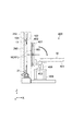
図1は、本発明の一実施形態に係る基板ホルダ100を概略的に示す正面図である。図2は、図1におけるA−A線方向の概略断面図である。
[Board holder]
FIG. 1 is a front view schematically showing a
なお各図においてX軸、Y軸及びZ軸は、相互に直交する3軸方向を示しており、本実施形態ではそれぞれ、基板ホルダ100の厚み方向、幅方向及び高さ方向に相当する。
In each figure, the X-axis, the Y-axis, and the Z-axis indicate three axial directions that are orthogonal to each other, and in the present embodiment, they correspond to the thickness direction, the width direction, and the height direction of the
基板ホルダ100は、後述する縦型基板搬送装置に用いられ、基板Wを略垂直な姿勢(起立姿勢)に保持した状態で搬送するためのキャリアとして構成される(図4)。
縦型基板搬送装置は、基板Wを垂直な姿勢で搬送するものに限られず、基板Wを鉛直方向に対して略5°程度傾斜させて搬送する場合も含む。すなわち上記起立姿勢には、文字どおり垂直な姿勢だけに限られず、ほぼ垂直な姿勢も含まれる。
上記縦型基板搬送装置は、後述する基板処理装置に適用される(図3)。基板処理装置は、例えば、インライン式スパッタ装置で構成される。基板Wは、典型的には矩形のガラス基板であり、その大きさは特に限定されず、例えば、G4ないしG6サイズのものが用いられる。
The
The vertical substrate transport device is not limited to the one that transports the substrate W in a vertical posture, and also includes the case where the substrate W is tilted by about 5 ° with respect to the vertical direction. That is, the above-mentioned standing posture is not limited to a literally vertical posture, but also includes a substantially vertical posture.
The vertical substrate transfer apparatus is applied to a substrate processing apparatus described later (FIG. 3). The substrate processing apparatus is composed of, for example, an in-line sputtering apparatus. The substrate W is typically a rectangular glass substrate, the size of which is not particularly limited, and for example, a G4 to G6 size substrate is used.
基板ホルダ100は、枠体10と、吸着部20とを有する。
The
(枠体)
枠体10は、縦方向に長辺を有する矩形の板状部材で構成され、典型的には、ステンレス鋼、アルミニウム合金等の金属材料で構成される。枠体10は、基板Wよりも大きな厚みで形成され、成膜源(本例ではスパッタカソード)に対向する表面101と、その反対側の裏面102とを有する(図2参照)。
(Frame body)
The
枠体10の面内には、基板Wを起立姿勢で収容することが可能な矩形の開口部11が設けられている。開口部11の周縁部には、基板Wの成膜領域を画定する枠状のマスク部12が設けられる。マスク部12は、開口部11の内周縁部の全域にわたって設けられ、枠体10の厚みより小さい厚みで形成される。
A
図2に示すように、マスク部12は、枠体10の表面101に連接される表面部121を有するとともに、先端部に向かって厚みが徐々に減少するように形成される。マスク部12の裏面部122は、枠体10の裏面102に段部を介して形成され、基板Wの成膜面W1の周縁部と対向する対向面13を構成する。これにより、枠体10の表面101からは基板Wの表面(成膜面W1)の周縁部を除く領域が外部へ露出され、枠体10の裏面102からは基板Wの裏面(非成膜面W2)の全域が露出される。
As shown in FIG. 2, the
対向面13は、基板Wの周縁部と基板Wの厚み方向に対向する平面で構成され、本実施形態では、マスク部12の一部(裏面部122)に設けられる。対向面13は、基板Wの成膜面W1の周縁部の全周にわたって対向するように構成されており、その面内には基板Wを静電的に吸着することが可能な吸着部20が設けられている。
The facing
(吸着部)
吸着部20は、対向面13に設けられ、基板Wの周縁部の少なくとも一部を静電的に吸着することが可能に構成される。吸着部20は、典型的には静電チャックで構成され、図1に示すように、対向面13に設けられた複数のチャック領域21に内蔵される。
(Adsorption part)
The
吸着部20は、各チャック領域21に設けられ、所定以上の電圧が印加されることで基板Wに対する静電吸着力を発現させるチャック電極を有する。静電吸着力の種類は特に限定されず、典型的には、クーロン力、ジョンソン・ラーベック力等が採用される。
The
吸着部20は、本実施形態では双極型静電チャックで構成され、各チャック領域21には正極用のチャック電極と負極用のチャック電極がそれぞれ設けられる。これら2つのチャック電極は、対向面13に面するように相互に隣接して配置される。各電極は絶縁膜で保護され、当該絶縁膜を介して基板Wと接触する。なお、吸着部20は、単極型静電チャックで構成されてもよい。
In the present embodiment, the
複数のチャック領域21は、対向面13の全周にわたってほぼ等間隔で構成される。図1の例では、基板Wの上縁及び下縁をそれぞれ3つのチャック領域21で保持し、基板Wの両側縁をそれぞれ4つのチャック領域21で保持する構成としたが、勿論これは一例であり、各チャック領域21の大きさ(面積)、配列数、配列形態等は、基板Wを起立姿勢で安定に保持できれば特に限定されない。
The plurality of
なお、チャック領域21は単数でもよい。この場合、チャック領域21は、基板Wの上半分を吸着するように半枠状に構成されてもよいし、基板Wの全周を吸着するように枠状に構成されてもよい。
The
基板ホルダ100はさらに、各チャック領域21(チャック用電極)に電力を供給することが可能な電源回路22を有する。電源回路22は、枠体10に設けられ、本実施形態では図1に示すように、枠体10の下端部112と開口部11との間に内蔵される。
The
電源回路22は、バッテリ221と、制御部222とを含む。バッテリ221は、典型的には充電可能な二次電池で構成され、例えばリチウムイオン二次電池で構成される。制御部222は、図示しないスイッチへの入力操作により、バッテリ221の電力を各チャック領域21へ供給することが可能に構成される。上記スイッチの切り替えは、例えば、基板処理装置における基板Wの受け渡し位置(ローディングポジション/アンローディングポジション)において操作される。
The
なお、制御部222は、CPU/MPUやメモリを含むコンピュータで構成されてもよい。この場合、所定位置において自動的にチャック領域21への電力供給及びその停止を切り替えることが可能となる。
The
電源回路22は、枠体10の内部に引き回された配線群23を介して各チャック領域21のチャック用電極へ電気的に接続される。電源回路22は、典型的には、各チャック領域21に対して電力供給及びその遮断を同期して行うように構成される。
The
これに代えて、所定のチャック領域21に対して個別に電力を供給するように構成されてもよい。これにより、各チャック領域21における吸着開始/解除動作を個々に制御することが可能となるため、反りや撓みが発生しやすい基板でも高い平面度を確保することができる。例えば、基板Wの上縁側から下縁側に向けて順次吸着動作が開始するように電力供給を制御することで、基板Wの自重をも利用しつつ、基板Wを所望とする平面度で安定に保持することが可能となる。
Instead of this, it may be configured to individually supply power to a
各チャック領域21は、電力の供給を受けて基板Wの保持動作を開始し、電力供給が遮断されて基板Wの保持動作を解除する。電源回路22は、基板Wの保持動作を速やかに行うため、デチャック操作時、チャック領域21へ逆電圧を印加するように構成されてもよい。
Each
[基板処理装置]
続いて、本実施形態に係る縦型基板搬送装置及び基板処理装置について説明する。
[Board processing equipment]
Subsequently, the vertical substrate transfer apparatus and the substrate processing apparatus according to the present embodiment will be described.
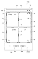
図3は、基板処理装置としてのインライン式スパッタ装置(以下、スパッタ装置という)200の構成を示す概略平面図である。 FIG. 3 is a schematic plan view showing the configuration of an in-line sputtering apparatus (hereinafter, referred to as a sputtering apparatus) 200 as a substrate processing apparatus.
図3に示すように、スパッタ装置200は、基板ホルダ100の搬送方向に順に、第1のロードロック室241、加熱室242、第1のスパッタ入口室243、第1のスパッタ室244、第1のスパッタ出口室245、第1の反転室246、第2のスパッタ入口室247、第2のスパッタ室248、第2のスパッタ出口室249、搬送室250及び第2のロードロック室251を有する。基板Wは、基板ホルダ100に保持された状態で、上記の各室へ起立姿勢で順次搬送される。第1の反転室246は、基板ホルダ100の搬送方向を180度反転させるためのものである。
As shown in FIG. 3, in the
加熱室242、第1及び第2のスパッタ入口室243,247、第1及び第2のスパッタ出口室245,249、第1の反転室246、及び搬送室250には真空ポンプPがそれぞれ接続されており、第1及び第2のスパッタ室244,248にはスパッタカソードSP1,SP2がそれぞれ配置されている。さらに、第1のロードロック室241と加熱室242との間、加熱室242と第1のスパッタ入口室243との間、第1のスパッタ出口室245と第1の反転室246との間、第1の反転室246と第2のスパッタ入口室247との間、第2のスパッタ出口室249と搬送室250との間、搬送室250と第2のロードロック室251との間にゲートバルブがそれぞれ配置されている。
A vacuum pump P is connected to the
上記の各室は、縦型基板搬送装置(以下、搬送装置という)300を構成する。図4は、図3におけるB−B線方向の概略断面図である。 Each of the above chambers constitutes a vertical substrate transfer device (hereinafter, referred to as a transfer device) 300. FIG. 4 is a schematic cross-sectional view taken along the line BB in FIG.
図4に示すように、搬送装置300は、基板ホルダ100と、基板ホルダ100を起立姿勢で搬送する搬送ユニット310とを有する。搬送ユニット310は、搬送室30(図示の例では、第1及び第2のスパッタ室244,248)と、駆動機構部31と、支持機構部32とを有する。
As shown in FIG. 4, the
駆動機構部31は、搬送室30の底部に設けられる。駆動機構部31は、基板ホルダ100の下端部112を支持する駆動ローラ311と、駆動ローラ311を回転させる駆動軸312と、駆動軸312を支持する支持部313と、駆動軸312を回転駆動するモータ314とを有する。駆動ローラ311は、基板ホルダ100の搬送方向に沿って所定の間隔で複数配置されており、基板ホルダ100を支持しながら下流側に向けて搬送する。
The
支持機構部32は、搬送室30の上部に設けられる。支持機構部32は、基板ホルダ100の上端部111に設けられたマグネット部113に対向する磁場発生部321と、基板ホルダ100の上端部111を挟んで搬送方向と直交する方向に対向する一対のガイド壁部322とを有する。磁場発生部321は、基板ホルダ100の搬送方向に沿って配列された複数の永久磁石で構成され、基板ホルダ100のマグネット部113を磁気吸引することで、基板ホルダ100の起立姿勢を保持する。一対のガイド壁部322は、基板ホルダ100の上端部111と間隔をおいて対向し、基板ホルダ100の所定角度以上の倒れを規制する。
The
図3を参照して、スパッタ装置200はさらに、大気室252と、基板受け渡し室253と、第2の反転室254とを有する。
With reference to FIG. 3, the
大気室252は、第1及び第2のロードロック室241,251に対してゲートバルブを介して接続される。大気室252は、第1のロードロック室241へ基板ホルダ100を搬入し、第2のロードロック室251から基板ホルダ100を搬出する。
The
基板受け渡し室253では、移載ユニット400によって、基板ホルダ100から処理済の基板Wが取り出され、基板ホルダ100へ未処理の基板Wが移載される。未処理の基板Wを保持した基板ホルダ100は、第2の反転室254で反転された後、大気室252を介して第1のロードロック室241へ搬送される。
In the
なお、基板受け渡し位置は上記の例に限定されず、種々変更が可能である。例えば、基板ホルダ100からの基板Wの取り出し位置と基板ホルダ100への基板Wの移載位置とは相互に異なっていてもよいし、基板Wの取り出し後(又は移載後)における基板ホルダ100の搬送ルートは、装置構成に応じて適宜決定することが可能である。
The substrate delivery position is not limited to the above example, and can be changed in various ways. For example, the position where the substrate W is taken out from the
図5は、移載ユニット400の一構成例を示す概略側面図である。
FIG. 5 is a schematic side view showing a configuration example of the
移載ユニット400は、基板Wを支持する支持テーブル401と、支持テーブル401を支持する基台404と、支持テーブル401と基台404との間に配置された支持ブロック405とを有する。
The
支持テーブル401は、基板Wの非成膜面W2(図2参照)を真空吸着可能な複数の吸着パッド402を有する。支持ブロック405は、支持テーブル401を基台404に対して略90度回動させる回動軸403を有するとともに、基台404に対して前後方向(図5においてX軸方向)に移動可能に構成される。移載ユニット400は、図5に示すように、支持テーブル401が基板Wを吸着保持した状態で、横臥姿勢と起立姿勢との間で略90度回動可能に構成される。また、移載ユニット400は、基板受け渡し室253内で支持体260によって起立状態が保持された基板ホルダ100に対して、支持テーブル401に吸着保持された基板Wを移載することが可能に構成される。
The support table 401 has a plurality of
[基板ホルダの動作]
続いて、以上のように構成される基板ホルダ100の動作について、スパッタ装置200の動作とともに説明する。
[Operation of board holder]
Subsequently, the operation of the
図5に示すように、基板受け渡し室253に搬送された基板ホルダ100は、その裏面102を移載ユニット400に向けて停止される。移載ユニット400は、支持テーブル401を横臥姿勢から起立姿勢に変換し、支持テーブル401上に吸着保持された未処理の基板Wの成膜面W1の周縁部を基板ホルダ100の対向面13に対向させた後、支持テーブル401を前進させて基板Wを対向面13に接触させる。このとき、基板ホルダ100は、その表面101が支持体40によって支持されているため、裏面102(対向面13)において基板Wを安定に受けることができる。
As shown in FIG. 5, the
基板ホルダ100の電源回路22は、吸着部20(各チャック領域21)へ電力を供給することで、基板Wに対する静電吸着動作を開始する。電源回路22による電力供給ONの切り替えは、図示しないスイッチに対する移載ユニット400による押圧等の入力操作で行われてもよいし、無線通信により非接触で行われてもよい。
The
各チャック領域21への電源供給のタイミングは、基板Wが対向面13に接触する前でもよいし、接触した後でもよい。さらに各チャック領域21における吸着動作のタイミングは、各々において同時に行われるが、これに限られない。
The timing of supplying power to each
支持テーブル401から基板ホルダ100への基板Wの移載が完了した後、支持テーブル401は元の後退位置へ復帰する。一方、基板ホルダ100は、基板Wを保持した状態で、第2の反転室254によって搬送方向が180度変換された後、大気室252を介して第1のロードロック室241へ搬送される。
After the transfer of the substrate W from the support table 401 to the
第1のロードロック室241へ搬入された基板ホルダ100は、加熱室242、第1のスパッタ入口室243及び第1のスパッタ室244へ順次搬送される。第1のスパッタ室244では、基板Wの成膜面W1にマスク部12を介して成膜処理が施される。マスク部12はその先端部に向かうに従って厚みが減少するように構成されているため(図2参照)、所望とするマスク精度が確保される。また、マスク部12の裏面部122に吸着部20(チャック領域21)が設けられているため、マスク部12と基板Wとの密着性が高まり、これによりマスク部12と基板Wとの間への成膜材料の回り込みが極力抑えられ、マスク精度のさらなる向上が図られる。
The
第1のスパッタ室244における成膜処理の完了後、基板ホルダ100は、第1のスパッタ出口室245、第1の反転室246、第2のスパッタ入口室247を介して第2のスパッタ室248へ搬送される。第2のスパッタ室248においても上述と同様な成膜処理が行われるが、必要に応じて省略されてもよい。その後、基板ホルダ100は、第2のスパッタ出口室249、搬送室250、第2のロードロック室251及び大気室252を介して、基板受け渡し室253へ再び搬送される。
After the film formation process in the
基板受け渡し室253において、成膜済の基板Wは、基板ホルダ100から移載ユニット400の支持テーブル401へ移載される。基板ホルダ100は、支持テーブル401の吸着パッド402が基板Wの非成膜面W2を吸着した後、電源回路22から各チャック領域21への電力供給を遮断し、基板Wの成膜面W1に対する静電吸着力を解除する。これにより、成膜済みの基板Wが基板ホルダ100から支持テーブル401へ移載される。
In the
電源回路22による電力供給OFFの切り替えは、図示しないスイッチに対する移載ユニット400による押圧等の入力操作で行われてもよいし、無線通信により非接触で行われてもよい。なお、上記静電吸着力の解除は、電源回路22から各チャック領域21へ保持時とは逆の電圧を印加することで実行されてもよい。
The power supply OFF switching by the
移載ユニット400は、支持テーブル401を横臥姿勢に変換した後、成膜済みの基板Wを他の移載ロボットへ移載した後、上述と同様な操作で、新たな未処理の基板Wが基板ホルダ100へ移載される。以後、上述の動作が繰り返し実行される。
In the
以上のように本実施形態によれば、基板ホルダ100は、基板Wの周縁部と対向する枠体10の対向面13に設けられた吸着部20(チャック領域21)によって基板Wを静電的に吸着するように構成されているため、クランプ機構を用いた基板保持構造と比較して、パーティクルの発生を抑えることができる。
As described above, according to the present embodiment, the
また、吸着部20(チャック領域21)が基板Wの成膜面W1の周縁部に対向する枠体10の対向面13に設けられているため、基板Wの非成膜面W2が開放状態に維持される。これにより、特別な位置決めを必要とすることなく移載ユニット400による基板Wの非成膜面W2へのアクセスが容易となり、枠体10に対する基板Wの着脱を迅速かつ確実に行うことが可能となる。
Further, since the suction portion 20 (chuck region 21) is provided on the facing
また、吸着部20(チャック領域21)が枠体10の対向面13の複数個所に設けられているため、基板Wをより安定的に保持することができる。さらに、電源回路22が枠体10に一体的に設けられているため、外部からの電源供給ラインの設置を不要とすることができる。
Further, since the suction portions 20 (chuck regions 21) are provided at a plurality of positions on the facing surfaces 13 of the
以上、本発明の実施形態について説明したが、本発明は上述の実施形態にのみ限定されるものではなく種々変更を加え得ることは勿論である。 Although the embodiments of the present invention have been described above, the present invention is not limited to the above-described embodiments, and it goes without saying that various modifications can be made.
例えば以上の実施形態では、基板ホルダ100の吸着部20が基板Wの成膜面W1の周縁部を吸着保持するように構成されたが、これに代えて、基板Wの非成膜面W2の周縁部を吸着保持するように構成されてもよい。これにより、基板Wの成膜面W1への全面成膜が可能となる。
For example, in the above embodiment, the
また、以上の実施形態において、基板ホルダ100の吸着部20(対向面13)は、枠体10の開口部11の周縁部にのみ形成されたが、これに限られず、例えば図6に示す基板ホルダ1100のように、枠体10の対辺間に開口部11を縦断する橋絡部14を設け、その橋絡部14にも吸着部20が設けられてもよい。橋絡部14の形態は特に限定されず、格子状、トラス状等のいずれであってもよい。例えば図6は、橋絡部14が十字状に形成されており、橋絡部14がマスク部として機能することで、基板Wの成膜面に4つの成膜領域が画定される例を示している。
Further, in the above embodiment, the suction portion 20 (opposing surface 13) of the
また以上の実施形態では、基板Wとしてガラス基板を例に挙げて説明したが、これに限られず、基板Wとして可撓性のプラスチックフィルム基板が用いられてもよい。この場合、上述のように基板ホルダ100の各吸着部20の吸着動作を同時に実行する代わりに、基板の上縁側から下縁側へ順に吸着動作を開始することで、基板の自重を利用しながら平面度の高い保持姿勢を得ることが可能となる。
Further, in the above embodiment, the glass substrate has been described as an example of the substrate W, but the present invention is not limited to this, and a flexible plastic film substrate may be used as the substrate W. In this case, instead of simultaneously executing the suction operations of the
さらに以上の実施形態では、基板ホルダ100の対向面13に吸着部20(チャック領域21)を単列で配置したが、これに限られず、吸着部20を多列で配置してもよい。これにより、基板Wに対する保持力を向上させることができる。この場合、各吸着部20は、対向面13上に千鳥足状に多列配置されてもよい。
Further, in the above embodiment, the suction portions 20 (chuck region 21) are arranged in a single row on the facing
10…枠体
11…開口部
12…マスク部
13…対向面
14…橋絡部
20…吸着部
21…チャック領域
22…電源回路
23…配線群
100,1100…基板ホルダ
200…スパッタ装置
300…縦型基板搬送装置
400…移載ユニット
W…基板
W1…成膜面
W2…非成膜面
10 ...
Claims (4)
前記基板の成膜面の周縁部と前記基板の厚み方向に対向する対向面を有する枠体と、
前記対向面に設けられチャック用電極をそれぞれ含む複数のチャック領域を有し、前記基板の成膜面の少なくとも上縁及び下縁を静電的に吸着することが可能に構成された吸着部と、
前記枠体に設けられ前記複数のチャック領域に個別に電力を供給することが可能な制御部を有する電源回路と、
を具備し、
前記制御部は、前記移載ユニットに支持された起立姿勢の前記基板の成膜面の周縁部が前記対向面に対向する状態で、前記基板の上縁側から下縁側に向けて順次吸着動作が開始するように、前記複数のチャック領域に対する電力供給を制御する
基板ホルダ。 A board holder used in a vertical board transfer device that can hold a board in an upright position supported by a transfer unit.
A frame body having a peripheral edge of a film-forming surface of the substrate and a facing surface facing the thickness direction of the substrate.
A suction portion provided on the facing surface and having a plurality of chuck regions including chuck electrodes, respectively, and capable of electrostatically adsorbing at least the upper edge and the lower edge of the film-forming surface of the substrate. ,
A power supply circuit provided in the frame and having a control unit capable of individually supplying electric power to the plurality of chuck regions.
Equipped with
The control unit sequentially performs a suction operation from the upper edge side to the lower edge side of the substrate in a state where the peripheral edge portion of the film-forming surface of the substrate in an upright posture supported by the transfer unit faces the facing surface. A substrate holder that controls the power supply to the plurality of chuck regions so as to start.
前記枠体は、前記基板の成膜領域を画定する枠状のマスク部をさらに有し、
前記対向面は、前記基板の周縁部と対向する前記マスク部の一部に設けられる
基板ホルダ。 The board holder according to claim 1.
The frame body further has a frame-shaped mask portion that defines a film-forming region of the substrate.
The facing surface is a substrate holder provided on a part of the mask portion facing the peripheral edge portion of the substrate.
前記基板の成膜面の周縁部と前記基板の厚み方向に対向する対向面を有する枠体と、前記対向面に設けられチャック用電極をそれぞれ含む複数のチャック領域を有し、前記基板の成膜面の少なくも上縁及び下縁を静電的に吸着することが可能に構成された吸着部と、前記枠体に設けられ前記複数のチャック領域に個別に電力を供給することが可能な制御部を有する電源回路と、を有する基板ホルダと、
前記基板ホルダを起立姿勢で搬送する搬送ユニットと
を具備し、
前記制御部は、前記移載ユニットに支持された起立姿勢の前記基板の成膜面の周縁部が前記対向面に対向する状態で、前記基板の上縁側から下縁側に向けて順次吸着動作が開始するように、前記複数のチャック領域に対する電力供給を制御する
縦型基板搬送装置。 A vertical substrate transfer device provided with a substrate holder capable of holding an upright substrate supported by a transfer unit.
A frame body having a facing surface that faces in the thickness direction of the peripheral portion and the substrate of the film-forming surface of the substrate has a plurality of chuck regions each including a chuck electrode provided on the facing surface, of the substrate formed It is possible to individually supply electric power to the suction portion configured to electrostatically suck at least the upper edge and the lower edge of the film surface, and to the plurality of chuck regions provided in the frame. A power supply circuit having a control unit, a board holder having a control unit, and
A transport unit for transporting the board holder in an upright position is provided .
The control unit sequentially performs a suction operation from the upper edge side to the lower edge side of the substrate in a state where the peripheral edge portion of the film-forming surface of the substrate in an upright posture supported by the transfer unit faces the facing surface. A vertical substrate transfer device that controls power supply to the plurality of chuck regions so as to start.
前記基板の成膜面の周縁部と前記基板の厚み方向に対向する対向面を有する枠体と、前記対向面に設けられチャック用電極をそれぞれ含む複数のチャック領域を有し、前記基板の成膜面の少なくも上縁及び下縁を静電的に吸着することが可能に構成された吸着部と、前記枠体に設けられ前記複数のチャック領域に個別に電力を供給することが可能な制御部を有する電源回路と、を有する基板ホルダと、
前記基板ホルダを起立姿勢で搬送する搬送ユニットと、
前記基板ホルダに保持された前記基板を処理する処理ユニットと
を具備し、
前記制御部は、前記移載ユニットに支持された起立姿勢の前記基板の成膜面の周縁部が前記対向面に対向する状態で、前記基板の上縁側から下縁側に向けて順次吸着動作が開始するように、前記複数のチャック領域に対する電力供給を制御する
基板処理装置。 A transfer unit that can support the board in an upright position,
A frame body having a facing surface that faces in the thickness direction of the peripheral portion and the substrate of the film-forming surface of the substrate has a plurality of chuck regions each including a chuck electrode provided on the facing surface, of the substrate formed It is possible to individually supply electric power to the suction portion configured to electrostatically suck at least the upper edge and the lower edge of the film surface, and to the plurality of chuck regions provided in the frame. A power supply circuit having a control unit, a board holder having a control unit, and
A transport unit that transports the board holder in an upright position,
A processing unit for processing the substrate held in the substrate holder is provided .
The control unit sequentially performs a suction operation from the upper edge side to the lower edge side of the substrate in a state where the peripheral edge portion of the film-forming surface of the substrate in an upright posture supported by the transfer unit faces the facing surface. A substrate processing apparatus that controls power supply to the plurality of chuck regions so as to start.
Priority Applications (3)
| Application Number | Priority Date | Filing Date | Title |
|---|---|---|---|
| JP2017003338A JP6851202B2 (en) | 2017-01-12 | 2017-01-12 | Board holder, vertical board transfer device and board processing device |
| CN201711472810.7A CN108300975A (en) | 2017-01-12 | 2017-12-29 | Substrate holder, vertical substrate conveying device and substrate board treatment |
| KR1020180002133A KR20180083259A (en) | 2017-01-12 | 2018-01-08 | Substrate holder, vertical type apparatus for transferring substrate and apparatus for processing substrate |
Applications Claiming Priority (1)
| Application Number | Priority Date | Filing Date | Title |
|---|---|---|---|
| JP2017003338A JP6851202B2 (en) | 2017-01-12 | 2017-01-12 | Board holder, vertical board transfer device and board processing device |
Publications (2)
| Publication Number | Publication Date |
|---|---|
| JP2018113361A JP2018113361A (en) | 2018-07-19 |
| JP6851202B2 true JP6851202B2 (en) | 2021-03-31 |
Family
ID=62867633
Family Applications (1)
| Application Number | Title | Priority Date | Filing Date |
|---|---|---|---|
| JP2017003338A Active JP6851202B2 (en) | 2017-01-12 | 2017-01-12 | Board holder, vertical board transfer device and board processing device |
Country Status (3)
| Country | Link |
|---|---|
| JP (1) | JP6851202B2 (en) |
| KR (1) | KR20180083259A (en) |
| CN (1) | CN108300975A (en) |
Families Citing this family (3)
| Publication number | Priority date | Publication date | Assignee | Title |
|---|---|---|---|---|
| CN109051686B (en) * | 2018-09-29 | 2020-08-04 | 苏州精濑光电有限公司 | Workpiece operation method |
| JP7242414B2 (en) * | 2019-05-08 | 2023-03-20 | 株式会社アルバック | Vacuum transfer device and film forming device |
| US20230058931A1 (en) * | 2020-02-27 | 2023-02-23 | Applied Materials Italia S.R.L. | Support device for supporting a substrate, method of processing a substrate and semiconductor substrate |
Family Cites Families (11)
| Publication number | Priority date | Publication date | Assignee | Title |
|---|---|---|---|---|
| JP4958406B2 (en) * | 2005-04-06 | 2012-06-20 | 株式会社アルバック | Handling method of glass substrate in vacuum atmosphere |
| JP4612516B2 (en) | 2005-09-29 | 2011-01-12 | 大日本印刷株式会社 | Sputtering device and carrier for sputtering device |
| JP2007134243A (en) * | 2005-11-11 | 2007-05-31 | Sony Corp | Method of manufacturing display device, and mask |
| JP5035499B2 (en) * | 2005-12-13 | 2012-09-26 | 大日本印刷株式会社 | Sputtering apparatus and carrier for substrate transfer |
| JP2007246983A (en) * | 2006-03-15 | 2007-09-27 | Seiko Epson Corp | Film deposition apparatus |
| CN101657563B (en) | 2007-04-18 | 2011-09-28 | 株式会社爱发科 | Dummy substrate, method for starting film forming apparatus using same, method for maintaining/changing film forming condition, and method for stopping apparatus |
| CN105579612B (en) * | 2013-09-20 | 2019-06-14 | 应用材料公司 | Substrate carrier with integral type electrostatic chuck |
| KR102237428B1 (en) * | 2014-02-14 | 2021-04-08 | 삼성디스플레이 주식회사 | Mask frame assembly and the manufacturing method thereof |
| JP2017516294A (en) * | 2014-05-09 | 2017-06-15 | アプライド マテリアルズ インコーポレイテッドApplied Materials,Incorporated | Substrate carrier system and method for using the same |
| WO2016167233A1 (en) * | 2015-04-15 | 2016-10-20 | 株式会社 アルバック | Substrate-holding mechanism, film formation device, and method for holding substrate |
| CN105568217B (en) * | 2016-01-06 | 2017-12-05 | 京东方科技集团股份有限公司 | Metal mask plate and preparation method thereof |
-
2017
- 2017-01-12 JP JP2017003338A patent/JP6851202B2/en active Active
- 2017-12-29 CN CN201711472810.7A patent/CN108300975A/en active Pending
-
2018
- 2018-01-08 KR KR1020180002133A patent/KR20180083259A/en active Search and Examination
Also Published As
| Publication number | Publication date |
|---|---|
| JP2018113361A (en) | 2018-07-19 |
| KR20180083259A (en) | 2018-07-20 |
| CN108300975A (en) | 2018-07-20 |
Similar Documents
| Publication | Publication Date | Title |
|---|---|---|
| KR101400453B1 (en) | Substrate conveyance method and substrate conveyance system | |
| JP6851202B2 (en) | Board holder, vertical board transfer device and board processing device | |
| JP6526795B2 (en) | Substrate holding method | |
| JP6640878B2 (en) | Substrate carrier and method of processing a substrate | |
| TWI684210B (en) | Method of processing a substrate, substrate carrier for holding a substrate and corresponding deposition apparatus | |
| TW202004967A (en) | Substrate carrier apparatus | |
| TWI712700B (en) | Sputtering apparatus | |
| JP5399084B2 (en) | Thin film forming system and thin film forming method | |
| TWI712102B (en) | Assembly for lifting or lowering a carrier, apparatus for transportation of a carrier in a vacuum chamber, and method for lifting or lowering a carrier | |
| JP2020025140A (en) | Device for forming semiconductor film on both sides of substrate | |
| JP4924520B2 (en) | Atmosphere cleaning device | |
| JPH11145266A (en) | Apparatus and method of electrostatic chucking, and apparatus and method of transferring substrate using the same | |
| TWI299964B (en) | ||
| JP7066475B2 (en) | Vacuum processing equipment | |
| JP5832372B2 (en) | Vacuum processing equipment | |
| JP3158463U (en) | Heat treatment equipment | |
| WO2020187412A1 (en) | Processing system, carrier for transporting a substrate in a processing system and method for transporting a carrier | |
| JP2012146844A (en) | Thin-film formation system | |
| TW200416882A (en) | Thin film forming apparatus, film supplier, film cassette, transport mechanism and transport method |
Legal Events
| Date | Code | Title | Description |
|---|---|---|---|
| A621 | Written request for application examination |
Free format text: JAPANESE INTERMEDIATE CODE: A621 Effective date: 20191029 |
|
| A977 | Report on retrieval |
Free format text: JAPANESE INTERMEDIATE CODE: A971007 Effective date: 20200813 |
|
| A131 | Notification of reasons for refusal |
Free format text: JAPANESE INTERMEDIATE CODE: A131 Effective date: 20200825 |
|
| A521 | Request for written amendment filed |
Free format text: JAPANESE INTERMEDIATE CODE: A523 Effective date: 20201021 |
|
| TRDD | Decision of grant or rejection written | ||
| A01 | Written decision to grant a patent or to grant a registration (utility model) |
Free format text: JAPANESE INTERMEDIATE CODE: A01 Effective date: 20210224 |
|
| A61 | First payment of annual fees (during grant procedure) |
Free format text: JAPANESE INTERMEDIATE CODE: A61 Effective date: 20210309 |
|
| R150 | Certificate of patent or registration of utility model |
Ref document number: 6851202 Country of ref document: JP Free format text: JAPANESE INTERMEDIATE CODE: R150 |
|
| R250 | Receipt of annual fees |
Free format text: JAPANESE INTERMEDIATE CODE: R250 |