JP6843556B2 - Image forming device - Google Patents
Image forming device Download PDFInfo
- Publication number
- JP6843556B2 JP6843556B2 JP2016166633A JP2016166633A JP6843556B2 JP 6843556 B2 JP6843556 B2 JP 6843556B2 JP 2016166633 A JP2016166633 A JP 2016166633A JP 2016166633 A JP2016166633 A JP 2016166633A JP 6843556 B2 JP6843556 B2 JP 6843556B2
- Authority
- JP
- Japan
- Prior art keywords
- charging
- image carrier
- toner
- image
- photosensitive drum
- Prior art date
- Legal status (The legal status is an assumption and is not a legal conclusion. Google has not performed a legal analysis and makes no representation as to the accuracy of the status listed.)
- Active
Links
Images


Description
本発明は、レーザープリンタ、複写機、ファクシミリ等の電子写真記録方式を利用する画像形成装置に関するものである。 The present invention relates to an image forming apparatus that utilizes an electrophotographic recording method such as a laser printer, a copier, or a facsimile.
従来、電子写真方式の画像形成装置において、像担持体としての感光ドラムを一様に帯電処理した後に、画像パターンに従った露光を行うことにより、感光ドラム上に静電潜像を形成する。その後、感光ドラム上の静電潜像をトナーで現像して顕在化し、紙などの記録材に転写する。そして、感光ドラム上に残った転写残トナーは、感光ドラム上から除去されて回収される。 Conventionally, in an electrophotographic image forming apparatus, an electrostatic latent image is formed on a photosensitive drum by uniformly charging a photosensitive drum as an image carrier and then performing exposure according to an image pattern. After that, the electrostatic latent image on the photosensitive drum is developed with toner to be manifested and transferred to a recording material such as paper. Then, the transfer residual toner remaining on the photosensitive drum is removed from the photosensitive drum and recovered.
転写残トナーを感光ドラム上から除去して回収する手段としては、クリーニングブレードなどのクリーニング部材を備えたクリーニング装置が広く用いられている。クリーニング装置により回収されたトナーは廃トナーとなるが、環境保全や資源の有効利用などの点から廃トナーは出ないことが望ましい。また、装置の小型化などの点から、クリーニング装置は設けられていないことが望ましい。 As a means for removing and recovering the transfer residual toner from the photosensitive drum, a cleaning device provided with a cleaning member such as a cleaning blade is widely used. The toner collected by the cleaning device becomes waste toner, but it is desirable that no waste toner is generated from the viewpoint of environmental protection and effective use of resources. Further, from the viewpoint of miniaturization of the device, it is desirable that no cleaning device is provided.
そこで近年、クリーニング装置を無くし、感光ドラム上の転写残トナーを現像装置によって「現像同時クリーニング」で感光ドラムから除去し、現像装置に回収し再利用する「クリーナレス方式」の画像形成装置の実用化がなされてきている。 Therefore, in recent years, a "cleanerless method" image forming apparatus has been put into practical use, in which the cleaning device is eliminated, the transfer residual toner on the photosensitive drum is removed from the photosensitive drum by "simultaneous development cleaning" by the developing device, and the toner is collected and reused in the developing device. It has been transformed.
一方、感光ドラムを帯電処理する手段としては、近年では帯電部材を像担持体に接触させ、この帯電部材に電圧を印加することで像担持体を帯電処理する接触帯電方式の採用が進んでいる。接触帯電方式は、コロナ帯電方式に比べて、帯電処理によるオゾンの発生量が少なく、また必要な電圧が低いため、環境や装置の小型化などの観点から好ましく、広く用いられるようになっている。 On the other hand, as a means for charging the photosensitive drum, in recent years, a contact charging method has been adopted in which a charging member is brought into contact with an image carrier and a voltage is applied to the charging member to charge the image carrier. .. Compared to the corona charging method, the contact charging method generates less ozone due to the charging process and requires a lower voltage, so that it is preferable from the viewpoint of the environment and miniaturization of the device, and is widely used. ..
ところで、クリーナーレス方式と接触帯電方式とを採用した画像形成装置においては、現像時の帯電極性とは逆極性に帯電した一部のトナーが帯電部材に付着し、これが蓄積することで帯電能力が劣化することがある。 By the way, in an image forming apparatus that employs a cleanerless method and a contact charging method, a part of toner charged with a polarity opposite to the charging polarity at the time of development adheres to a charging member, and the accumulated toner increases the charging ability. May deteriorate.
そこで、そのトナーを現像部において回収させる構成が開示されている。特許文献1では、非画像形成時の清掃動作において、帯電部材に付着した正極性に帯電したトナーを感光ドラムに転移させ、その転移したトナーを現像部材から感光ドラムに向かう方向に静電的に付勢した状態で現像部を通過させる。そして、その通過したトナーの帯電極性を帯電部において負極性に反転させ、そのトナーを現像部において回収させている。
Therefore, a configuration is disclosed in which the toner is collected in the developing unit. In
しかしながら、特許文献1に開示されているようなクリーナレス方式と接触帯電方式とを採用した画像形成装置において、非画像形成時の帯電部材の清掃動作中に、現像部材から感光ドラムにカブリトナーを転移させてしまうという課題があった。
However, in an image forming apparatus that employs a cleanerless method and a contact charging method as disclosed in
具体的には、帯電部材に付着した正極性に帯電したトナーを感光ドラムに転移させるために、帯電印加バイアスをHIGHからLOWに切り替える。その際に、感光ドラムと帯電部材との間の電位差が放電開始電圧Vth以上となり、感光ドラムから帯電部材への逆放電が生じ、帯電部材を通過後の感光ドラムの表面電位が低下する。このとき、感光ドラムの表面電位は逆放電によって不安定となり、局所的に表面電位の絶対値が大きい部分と小さい部分が発生する。したがって、感光ドラムの表面電位の低下に応じて現像部材に印加するバイアス値を可変とした場合でも、現像部における白地部コントラスト(以下Vbackと称する)が局所的に大きい部分と小さい部分が存在する。 Specifically, the charging application bias is switched from HIGH to LOW in order to transfer the positively charged toner adhering to the charging member to the photosensitive drum. At that time, the potential difference between the photosensitive drum and the charging member becomes equal to or higher than the discharge start voltage Vth, reverse discharge occurs from the photosensitive drum to the charging member, and the surface potential of the photosensitive drum after passing through the charging member decreases. At this time, the surface potential of the photosensitive drum becomes unstable due to the reverse discharge, and a portion having a large absolute value and a portion having a small absolute value of the surface potential are locally generated. Therefore, even when the bias value applied to the developing member is made variable according to the decrease in the surface potential of the photosensitive drum, there are a portion where the white background contrast (hereinafter referred to as Vback) in the developing portion is locally large and a portion where it is small. ..
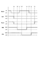
ここで、Vbackに対する感光ドラム上のカブリ曲線を図5に示す。図5に示す通り、VbackがΔ100〜300V程度であれば、反転カブリ領域にかかるものの、感光ドラム上のカブリ量(%)は少ない。しかし、VbackがΔ100V以下になると急激に地カブリトナーが発生しはじめ、Δ0Vになると大量の地カブリトナーが現像部材から感光ドラム上に転移する。したがって、感光ドラムから帯電部材への逆放電によってVbackが局所的にΔ0V近辺になった部分において地カブリトナーが発生し、この地カブリトナーが転写部材を汚す、或いは転写ニップ部において地カブリトナーが飛散して機内を汚し、最終的に裏汚れといった画像不良に至ってしまう。またこの地カブリトナーを再度現像部材で回収するための清掃時間を要することになり、結果的に画像形成装置の本体寿命を縮めることになる。 Here, the fog curve on the photosensitive drum with respect to Vback is shown in FIG. As shown in FIG. 5, when Vback is about Δ100 to 300V, the amount of fog (%) on the photosensitive drum is small, although it covers the inverted fog region. However, when Vback becomes Δ100V or less, ground fog toner suddenly begins to be generated, and when it becomes Δ0V, a large amount of ground fog toner is transferred from the developing member onto the photosensitive drum. Therefore, the ground fog toner is generated in the portion where the Vback is locally around Δ0V due to the reverse discharge from the photosensitive drum to the charging member, and this ground fog toner stains the transfer member, or the ground fog toner is generated in the transfer nip portion. It scatters and stains the inside of the aircraft, eventually leading to image defects such as back stains. Further, it takes a cleaning time to collect the ground fog toner again by the developing member, and as a result, the life of the main body of the image forming apparatus is shortened.
本発明の目的は、画像形成装置の本体内の汚れやそれに伴う裏汚れといった画像不良を防止し、さらにはカブリトナーを現像回収するための清掃時間を短縮することである。 An object of the present invention is to prevent image defects such as stains inside the main body of an image forming apparatus and back stains associated therewith, and to shorten the cleaning time for developing and recovering fog toner.
上記目的を達成するため、本発明は、
回転可能な像担持体と、
回転可能であって、前記像担持体と接触して前記像担持体と共に帯電部を形成し、前記帯電部において前記像担持体の表面を帯電する帯電部材と、
帯電された前記像担持体の表面を露光して静電像を形成する露光部と、
前記像担持体と接触して前記像担持体と共に現像部を形成し、前記現像部において前記像担持体の表面上の前記静電像に正規極性に帯電したトナーを供給してトナー像を形成する現像部材と、
前記帯電部材に帯電電圧を印加する帯電電圧印加部と、
前記露光部と前記帯電電圧印加部を制御する制御部と、を有し、
以下の(i)〜(v)の工程を含む、前記帯電部材に付着した前記トナーを前記帯電部材から前記像担持体に移動させて前記帯電部材を清掃する清掃動作を実行可能であることを特徴とする画像形成装置、
(i)前記像担持体が回転し、前記正規極性とは逆極性に帯電されたトナーに前記帯電部材から前記像担持体に向かう方向の静電気力が作用する向きの電位差が前記帯電部材と前記像担持体との間に形成されるように前記帯電電圧が印加された前記帯電部を、前記像担持体の領域が通過する第1の工程、
(ii)前記第1の工程を経た前記像担持体の表面が、前記露光部により画像形成動作における露光量より小さい露光量で露光される第2の工程、
(iii)前記逆極性に帯電されたトナーに前記現像部材から前記像担持体に向かう方向の静電気力が作用する向きの電位差が前記現像部材と前記像担持体との間に形成された前記現像部を、前記第2の工程を経た前記領域が通過する第3の工程、
(iv)前記逆極性に帯電されたトナーに前記像担持体から前記帯電部材に向かう方向の静電気力が作用する向きの電位差であって、前記帯電部材と前記像担持体の間で放電が発生する大きさの電位差が前記帯電部材と前記像担持体との間に形成されるように前記帯電電圧が印加された前記帯電部を、前記第3の工程を経た前記領域が通過する第4の工程、
(v)前記正規極性に帯電されたトナーに前記像担持体から前記現像部材に向かう方向の静電気力が作用する向きの電位差が前記現像部材と前記像担持体との間に形成された前記現像部を、前記第4の工程を経た前記領域が通過する第5の工程。
In order to achieve the above object, the present invention
With a rotatable image carrier,
A charging member that is rotatable and comes into contact with the image carrier to form a charged portion together with the image carrier and charges the surface of the image carrier at the charged portion.
An exposed portion that exposes the surface of the charged image carrier to form an electrostatic image,
In contact with the image carrier, a developing section is formed together with the image carrier, and the developing section supplies toner charged to the electrostatic image on the surface of the image carrier to form a toner image. With the developing member
A charging voltage application unit that applies a charging voltage to the charging member,
It has a control unit that controls the exposure unit and the charging voltage application unit.
It is possible to perform a cleaning operation including the following steps (i) to (v) in which the toner adhering to the charging member is moved from the charging member to the image carrier to clean the charging member. Characteristic image forming apparatus,
(I) The potential difference in the direction in which the image carrier rotates and the electrostatic force in the direction from the charging member toward the image carrier acts on the toner charged in the opposite polarity to the normal polarity is the difference between the charging member and the charging member. The first step, in which the region of the image carrier passes through the charged portion to which the charging voltage is applied so as to be formed between the image carrier and the image carrier.
(Ii) A second step in which the surface of the image carrier that has undergone the first step is exposed by the exposed portion with an exposure amount smaller than the exposure amount in the image forming operation .
(Iii) The development in which a potential difference in the direction in which an electrostatic force in the direction from the developing member toward the image carrier acts on the toner charged in the opposite polarity is formed between the developing member and the image carrier. A third step in which the region that has undergone the second step passes through the portion,
(Iv) A potential difference in the direction in which an electrostatic force in the direction from the image carrier toward the charging member acts on the toner charged in the opposite polarity, and a discharge is generated between the charging member and the image carrier. A fourth portion of the region that has undergone the third step passes through the charged portion to which the charging voltage is applied so that a potential difference of such a magnitude is formed between the charging member and the image carrier. Process,
(V) The development in which a potential difference in the direction in which an electrostatic force in the direction from the image carrier toward the developing member acts on the toner charged to the normal polarity is formed between the developing member and the image carrier. A fifth step in which the region that has undergone the fourth step passes through the unit.
本発明によれば、画像形成装置の本体内の汚れやそれに伴う裏汚れといった画像不良を防止し、さらにはカブリトナーを現像回収するための清掃時間を短縮することができる。 According to the present invention, it is possible to prevent image defects such as stains inside the main body of the image forming apparatus and back stains associated therewith, and further to shorten the cleaning time for developing and recovering fog toner.
以下、図面を参照して、本発明の好適な実施の形態を例示的に詳しく説明する。ただし、以下の実施形態に記載されている構成部品の寸法、材質、形状、それらの相対配置などは、本発明が適用される装置の構成や各種条件により適宜変更されるべきものである。従って、特に特定的な記載がない限りは、本発明の範囲をそれらのみに限定する趣旨のものではない。 Hereinafter, preferred embodiments of the present invention will be described in detail exemplarily with reference to the drawings. However, the dimensions, materials, shapes, relative arrangements, and the like of the components described in the following embodiments should be appropriately changed depending on the configuration of the apparatus to which the present invention is applied and various conditions. Therefore, unless otherwise specified, the scope of the present invention is not intended to be limited to them.
〔実施例1〕
<画像形成装置>
図1を用いて、画像形成装置100の概略構成について説明する。図1は画像形成装置100の概略構成図である。
[Example 1]
<Image forming device>
The schematic configuration of the
本実施例の画像形成装置100は、クリーナレス方式と接触帯電方式とを採用した電子写真方式の画像形成装置であり、ここではレーザビームプリンタを例示している。
The
画像形成装置100は、回転可能な像担持体としてのドラム型(円筒形)の電子写真感光体である感光ドラム1を有する。画像出力動作が開始されると、感光ドラム1は、不図示の駆動モータによって図中矢印R1方向に回転駆動される。回転する感光ドラム1の表面は、帯電手段としてのローラ型の帯電部材である帯電ローラ2によって、所定の極性(本実施例では負極性)の所定の電位に一様に帯電処理される。帯電ローラ2は、感光ドラム1に接触して配置され、駆動モータによって図中矢印R2方向に回転駆動される。このとき、帯電ローラ2には、帯電電圧印加手段としての帯電電源E1(図2)から、負極性の直流電圧である所定の帯電電圧(帯電バイアス)が印加される。感光ドラム1と帯電ローラ2との接触部が帯電ニップaである。また、感光ドラム1の回転方向において、感光ドラム1上の帯電ローラ2によって帯電処理される位置が帯電部である。帯電ローラ2は、感光ドラム1の回転方向における帯電ニップaの上流側及び下流側の帯電ローラ2と感光ドラム1との間に形成される空隙のうち少なくとも一方で生じる放電により、感光ドラム1の表面を帯電処理する。本実施例では、理解を容易とするために、帯電ニップにおいて感光ドラム1の表面の帯電処理が行われるものと擬制して、帯電ニップを帯電部aとして説明することがある。
The
帯電処理された感光ドラム1の表面は、像露光手段(静電像形成手段)としての露光装置(レーザ露光ユニット)3によって、画像データに応じて変調されたレーザビームLで走査露光される。露光装置3は、レーザビームLにより感光ドラム1の主走査方向(回転軸方向)に露光を繰り返しつつ、副走査方向(表面移動方向)にも露光を行うことで、感光ドラム1上に静電潜像を形成する。感光ドラム1の回転方向において、感光ドラム1上の露光装置3による露光位置が像露光部bである。
The surface of the charged
感光ドラム1上に形成された静電潜像は、現像手段としての現像装置4によって、現像剤としてのトナーを用いてトナー像として現像(可視化)される。現像装置4は、現像容器45と、回転自在に現像容器45に支持された現像部材(現像剤担持体)としての現像スリーブ41と、を有している。現像容器45には、現像剤としての磁性一成分現像剤であるブラック色のトナーTが収容されている。本実施例のトナーTは、負帯電特性のものである。すなわち、本実施例では、トナーTの正規極性(現像時の帯電極性)は負極性である。現像スリーブ41は、現像容器45の感光ドラム1と対向する位置に設けられた開口部に、一部が外部に露出するようにして配置されている。現像スリーブ41は、中空の非磁性金属(アルミなど)素管の周囲に所定の体積抵抗を持つ導電性弾性ゴム層を設けたものである。現像スリーブ41の中空部には、磁界発生手段としてのマグネットローラ43が固定され配置されている。
The electrostatic latent image formed on the
現像容器45に収容されたトナーTは、撹拌部材44によって撹拌されると共に、マグネットローラ43の磁力により現像スリーブ41の表面に供給される。現像スリーブ41の表面に供給されたトナーTは、現像スリーブ41の回転に伴って現像剤規制手段としての現像ブレード42との対向部を通過することで、均一に薄層化され、また摩擦帯電により負極性に帯電させられる。その後、現像スリーブ41上のトナーは、現像スリーブ41の回転に伴って感光ドラム1と接触する現像位置まで搬送され、感光ドラム1上の静電潜像に応じて感光ドラム1に転移し、感光ドラム1上の静電潜像を現像する。このとき、現像スリーブ41には、現像電圧印加手段としての現像電源E2(図2)から、負極性の直流電圧である所定の現像電圧(現像バイアス)が印加される。本実施例では、イメージ部露光と反転現像により、トナー像が形成される。すなわち、一様に帯電処理された後に露光されることによって電位の絶対値が小さくなった感光ドラム1上の露光部(画像部)に、感光ドラム1の帯電電位と同極性(本実施例では負極性)に帯電したトナーが付着する。
The toner T contained in the developing
感光ドラム1の回転方向において、感光ドラム1上の現像スリーブ41と対向(接触)する位置が現像部cである。
In the rotation direction of the
尚、本実施例では、現像スリーブ41は、現像部cにおいて感光ドラム1と現像スリーブ41との移動方向が同方向となるように、不図示の駆動モータによって図中矢印R3方向に回転駆動される。
In this embodiment, the developing
感光ドラム1上に形成されたトナー像は、感光ドラム1と、転写手段としてのローラ型の転写部材である転写ローラ5と、の接触部である転写部dに送られる。また、感光ドラム1上のトナー像とタイミングを合わせて、収容部8から搬送ローラ9などによって、被転写体である記録用紙などの記録材Pが、転写部dに搬送されてくる。そして、感光ドラム1上のトナー像は、転写部dにおいて、転写ローラ5の作用により、感光ドラム1と転写ローラ5とに挟持されて搬送される記録材P上に転写される。このとき、転写ローラ5には、転写電圧印加手段としての転写電源E3(図2)から、トナーの正規極性とは逆極性(本実施例では正極性)の直流電圧である所定の転写電圧(転写バイアス)が印加される。これにより転写ローラ5と感光ドラム1との間に形成される電界の作用により、感光ドラム1から記録材Pへとトナー像が静電的に転写される。
The toner image formed on the
トナー像が転写された記録材Pは、定着手段としての定着装置7に送られる。定着装置7において、記録材Pには熱及び圧力が加えられ、記録材Pに転写されたトナー像は記録材Pに定着される。
The recording material P to which the toner image is transferred is sent to the
一方、記録材Pに転写されずに感光ドラム1上に残った転写残トナー(残留トナー)は、現像同時クリーニングにより現像装置4に回収される。つまり、現像装置4は、電圧が印加されて現像部cで感光ドラム1上の静電像に負極性に帯電したトナーTを供給する機能と、転写の後に感光ドラム1上に残った転写残トナーを回収する機能とを兼ねている。現像同時クリーニングの詳細については後述する。
On the other hand, the transfer residual toner (residual toner) remaining on the
ここで、画像形成装置100は、不図示の外部機器からの指示により開始される、単一又は複数の記録材Pに画像を形成する一連の画像出力動作(ジョブ)を行う。ジョブは、一般に、画像形成工程(印字工程)、前回転工程、複数の記録材Pに画像を形成する場合の紙間(記録材間)工程、及び後回転工程を有する。画像形成工程は、実際に感光ドラム1への静電潜像の形成、静電潜像の現像、トナー像の転写、トナー像の定着などを行う期間であり、より詳細には、帯電、露光、現像、転写、定着などの各工程が行われる位置により画像形成工程のタイミングは異なる。前回転工程は、画像形成工程の前の準備動作を行う期間である。紙間工程は、複数の記録材Pに対して画像形成工程を連続して行う際の、転写部dにおける記録材Pと記録材Pとの間に対応する期間である。後回転工程は、画像形成工程の後の整理動作(準備動作)を行う期間である。上記画像形成工程が画像形成時であり、該画像形成時以外の期間(前回転工程、紙間工程、後回転工程など)が非画像形成時である。そして、本実施例では、非画像形成時の所定のタイミングで、転写ローラ5に付着したトナーを感光ドラム1上に吐き出す清掃動作が実行される。
Here, the
<現像同時クリーニング>
現像同時クリーニングの詳細について説明する。本実施例における画像形成装置100は、感光ドラム1の回転方向において転写部dより下流側かつ帯電部aより上流側に、感光ドラム1を除電処理する除電手段としての前露光装置6を設けている。前露光装置6は、帯電部aで安定した放電を生じさせるために、帯電部aに進入する前の感光ドラム1の表面電位を光除電する。感光ドラム1の回転方向において、前露光装置6による露光位置が除電部eである。転写残トナーは、正極性に帯電しているトナーや、負極性に帯電しているものの充分な電荷を有していないトナーが混在する。これらトナーに対しては、前露光装置6により転写後の感光ドラム1を除電し、帯電処理時に均一な放電を生じさせることによって、再び負極性に帯電させることが可能となる。
<Simultaneous development cleaning>
The details of simultaneous development cleaning will be described. The
帯電部aにおいて負極性に帯電させられたトナーは、感光ドラム1の回転に伴い現像部cに送られる。現像部cに送られてきたトナーは、非画像領域(非露光領域)は、感光ドラム1の表面の暗部電位(Vd)と、現像バイアス(Vdc)との電位差により現像スリーブ41に転移し、現像装置4に回収される。一方、画像領域(露光領域)は、感光ドラム1の表面の明部電位(Vl)と、現像バイアス(Vdc)との電位差により現像スリーブ41には転移せず、そのまま画像部として感光ドラム1の回転に伴い転写部dに送られ、記録材Pに転写される。なお、Vdcは、VdとVlとの間の電位に設定される。
The toner charged negatively in the charging unit a is sent to the developing unit c as the
<制御態様>
図2は、画像形成装置100の要部の概略制御態様を示すブロック図である。画像形成装置100に設けられた制御手段としての制御部150は、演算処理を行う中心的素子であるCPU151、記憶素子であるROM、RAMなどのメモリ152などを有して構成される。RAMには、センサの検知結果、演算結果などが格納され、ROMには制御プログラム、予め求められたデータテーブルなどが格納されている。制御部150は、画像形成装置100の動作を統括的に制御する制御手段であり、各種の電気的情報信号の授受や、駆動のタイミングなどを制御しており、所定の作像シーケンス制御などを司る。制御部150には、画像形成装置100における各制御対象が接続されている。例えば、制御部150には、帯電電源E1、現像電源E2、転写電源E3、前露光装置6などが接続されている。特に、本実施例との関係で言えば、制御部150は、各種電源E1、E2、E3のON/OFFや出力値、前露光装置6による除電光の照射のON/OFFなどを制御して、後述する転写ローラ5の清掃動作を実行させる。
<Control mode>
FIG. 2 is a block diagram showing a schematic control mode of a main part of the
<帯電ローラの清掃動作>
上述のように、転写残トナーは、帯電部aにおいて負極性に帯電させられて、帯電部aを通過して現像部cへと送られるようになっている。しかし、一部、帯電部aで充分に負極性とならずに帯電ローラ2に付着し続けるトナーがある。このトナーが帯電ローラ2に付着した状態で画像形成を続けると、帯電ローラ2へトナーが固着することによる帯電性能の低下などが生じることがある。そのため、所定のタイミングで、帯電ローラ2に付着したトナーを感光ドラム1に付着させて現像部cに送り、現像装置4に戻すことが望まれる。しかし、本発明者らの検討により、帯電ローラ2へのトナー付着に関して、次のことがわかった。つまり、帯電ローラ2にトナーが付着してしまうと、帯電ローラ2からの放電により感光ドラム1を帯電させる際に、その放電現象により帯電ローラ2に付着しているトナーは正極性成分が増える。そのため、摩擦によってトナーの帯電極性を負極性に反転させようとしても、正極性に帯電したトナーを充分に負極性に反転させることができない場合がある。
<Cleaning operation of charging roller>
As described above, the transfer residual toner is negatively charged in the charging section a, passes through the charging section a, and is sent to the developing section c. However, there are some toners that continue to adhere to the charging roller 2 without being sufficiently negative in the charging portion a. If the image formation is continued with the toner adhering to the charging roller 2, the charging performance may be deteriorated due to the toner sticking to the charging roller 2. Therefore, it is desired that the toner adhering to the charging roller 2 is adhered to the
そこで、本実施例では、制御部150は、非画像形成時の所定のタイミングで、次のような帯電ローラ2に付着したトナーを減少させる清掃動作を実行させる。すなわち、制御部150は、清掃動作において、感光ドラム1を回転させながら、帯電ローラ2に付着した正極性に帯電したトナーを帯電ローラ2から感光ドラム1に静電的に転移させる。また、制御部150は、その転移したトナーを現像スリーブ41から感光ドラム1に向かう方向に静電的に付勢した状態で現像部cを通過させる。また、制御部150はその通過したトナーの帯電極性を帯電部aにおいて負極性に反転させる。そして、制御部150は、その帯電極性が反転させられたトナーを現像部cにおいて感光ドラム1から現像スリーブ41に静電的に転移させて現像装置4に回収させる。以下、更に詳しく説明する。
Therefore, in this embodiment, the
本実施例では、帯電ローラ2に付着した正極性に帯電したトナーを、正極性に帯電したまま感光ドラム1に静電的(電界的)に付着させる。つまり、帯電ローラ2に印加する電圧を、感光ドラム1の表面電位に対し正極性側の電圧にすることで、正極性に帯電したままトナーを静電的に帯電ローラ2から感光ドラム1に付着させる。そして、感光ドラム1に付着した正極性に帯電したトナーを、その帯電極性によって現像部cではほとんど現像装置4へは回収させずに現像部cを通過させる。その後、正極性に帯電したトナーを付着させた感光ドラム1の領域を帯電ローラ2からの放電により帯電処理すると共に、その正極性に帯電したトナーの帯電極性を負極性に反転させる。このとき、本実施例では、正極性に帯電したトナーを付着させた感光ドラム1の領域は、前露光装置6により光除電した後に、帯電ローラ2により帯電処理する。そして、負極性に帯電させられたトナーは、帯電部aを通過した後に、現像部cにおいて現像スリーブ41に静電的に転移されて、現像装置4に回収される。
In this embodiment, the positively charged toner adhering to the charging roller 2 is electrostatically (electrically) attached to the
図3は、本実施例の帯電ローラ2の清掃動作のタイミングチャート図である。帯電ローラ2の清掃動作は、制御部150により図3に示すタイミングで各部の動作が制御されることで実行される。本実施例では、画像出力枚数が所定の閾値以上となった場合に、後回転(非画像形成時)において帯電ローラ2の清掃動作が実行される。
FIG. 3 is a timing chart of the cleaning operation of the charging roller 2 of this embodiment. The cleaning operation of the charging roller 2 is executed by controlling the operation of each unit at the timing shown in FIG. 3 by the
・タイミング(a):
図3における(a)は、印字工程における像露光が終了して感光ドラム1上に形成されたトナー像が転写部dを通過したタイミングであり、このタイミングで転写バイアスをHIGHからLOWにする。転写バイアスをLOWにすることで、転写ローラ5からの電荷流入をなくし、転写部dを通過した後の感光ドラム1の表面電位の低下を抑制する。それとともに、前露光装置6をOFFにして、帯電部aに到達する前の光除電による感光ドラム1の表面電位の低下をなくす。このように、転写バイアスをLOWにして、前露光装置6をOFFにすることで、感光ドラム1の表面電位を保つようにする。なお、印字工程が終了した後も、帯電バイアス及び現像バイアスは、HIGHのままとされている。すなわち、帯電ローラ2に所定の帯電電圧を印加させて感光ドラム1を帯電処理させると共に、その帯電処理された感光ドラム1の領域が現像部cを通過する際に現像スリーブ41に所定の現像電圧を印加させる。
-Timing (a):
FIG. 3A shows the timing at which the toner image formed on the
・タイミング(b):
次に、転写バイアスがLOWの状態で転写部dを通過し、かつ、前露光装置6がOFFの状態で除電部eを通過した感光ドラム1の領域が帯電部aに到達するタイミングで、帯電バイアスをHIGHからLOWにする。これにより、帯電バイアスは、感光ドラム1の表面電位よりも正極性側に高い電圧(例えば、感光ドラム1の表面電位と同極性で絶対値が小さい電圧)となる。本実施例では、このとき帯電ローラ2に印加するLOWの帯電バイアスは、帯電部aにおける感光ドラム1と帯電ローラ2との間の電位差が放電開始電圧Vth以上になるように設定される。そのため、感光ドラム1から帯電ローラ2への逆放電が生じて、感光ドラム1の表面電位の絶対値が小さくなる。つまり、感光ドラム1の表面電位の絶対値は、帯電部aを通過することで、帯電部aに到達する直前よりも小さくなる。そして、帯電ローラ2に付着している正極性に帯電したトナーが、正極性に帯電したまま感光ドラム1に静電的に付着する。また、帯電ローラ2上の極性をもたない少量のトナーは、上記逆放電により負極性に帯電する。すなわち、帯電ローラ2に印加する電圧を、(a)工程で帯電処理された感光ドラム1の領域が帯電部aを通過する際に、その領域が帯電部aに到達する際の表面電位よりも正極性側に高い電圧に変更する。
・ Timing (b):
Next, the region of the
・タイミング(c):
次に、タイミング(b)で正極性に帯電したトナーが付着した感光ドラム1の領域が像露光部bに到達するタイミングで、トナーが付着している領域の全域を全面露光する。全面露光とは、印字工程中の像露光と同じ光量を感光ドラム1の長手全域に露光することである。これにより、感光ドラム1の全面露光された領域の表面電位の絶対値が一様に小さくなる。つまり、感光ドラム1の表面電位の絶対値は、像露光部bを通過することで、像露光部bに到達する直前よりも一様に小さくなる。この全面露光によって、タイミング(b)〜(c)間に感光ドラム1から帯電ローラ2への逆放電によって不安定となっている感光ドラム1の表面電位を安定させることができる。また、このとき感光ドラム1に静電的に付着している正極性に帯電したトナーは、像露光部bを通過後も感光ドラム1に静電的に付着している。
・ Timing (c):
Next, at the timing when the region of the
・タイミング(d):
次に、タイミング(c)で全面露光を受けた感光ドラム1の領域が現像部cに到達するタイミングで、現像バイアスをHIGHからLOWにする。つまり、前記全面露光により感光ドラム1の表面電位の絶対値が一様に小さくなっている。そのため、それに対応して、現像バイアスを、感光ドラム1の表面電位よりもさらに正極性側に高い電圧(例えば、感光ドラム1の表面電位と同極性で絶対値が小さい電圧)とするように、現像バイアスをLOWにする。現像バイアスをLOWにすることで、感光ドラム1上の正極性に帯電したトナーの大部分は、現像スリーブ41から感光ドラム1に向けて静電的に付勢された状態で現像部cを通過する。なお、このとき感光ドラム1上の正極性に帯電したトナーの一部が現像装置4に回収されてもよい。すなわち、現像スリーブに印加する電圧を、(c)工程によって表面電位の絶対値が一様に小さくなった感光ドラムの領域が現像部cを通過する際に、上記所定の現像電圧よりも正極性側に高い電圧に変更する。
-Timing (d):
Next, the development bias is changed from HIGH to LOW at the timing when the region of the
・タイミング(e):
次に、帯電バイアスがLOWの状態で帯電ローラ2を1周分以上回転させた後に、帯電バイアスをHIGHに戻す。感光ドラム1の表面電位に対し帯電バイアスを負極性側に高い電圧にする(同極性で絶対値を大きくする)ことで、LOWの帯電バイアスの印加によって帯電ローラ2に残った少量の負極性に帯電したトナーを、静電的に感光ドラム1に付着させる。なお、帯電バイアスをLOWからHIGHに戻すタイミングは、帯電ローラ2の全周の清掃を可能とするために、少なくとも帯電ローラ2の1周後であることが好ましい。なお、ここで変更された後のHIGHの帯電バイアスは、LOWに変更される前の電圧に限定されるものではなく、LOWの帯電バイアスよりも負極性側に高い電圧であればよい。すなわち、帯電ローラ2に印加する電圧を、(b)工程の変更後の電圧を帯電ローラ2に印加している際に帯電部aを通過した感光ドラム1の領域が帯電部aを通過する際に、(b)工程の変更後の電圧よりも負極性側に高い電圧に変更する。
・ Timing (e):
Next, after rotating the charging roller 2 for one round or more while the charging bias is LOW, the charging bias is returned to HIGH. By setting the charging bias to a higher voltage on the negative electrode side with respect to the surface potential of the photosensitive drum 1 (increasing the absolute value with the same polarity), a small amount of negative electrode property remaining on the charging roller 2 due to the application of the LOW charging bias. The charged toner is electrostatically attached to the
・タイミング(f):
次に、帯電バイアスをHIGHに戻した状態で帯電部aを通過した感光ドラム1の領域が像露光部bに到達するタイミングで、露光装置3をOFFして感光ドラム1上の全面露光を停止する。これにより、像露光部bを通過後の感光ドラム1の表面電位を保つようにする。つまり、感光ドラム1は帯電バイアスをHIGHに戻した後の帯電処理後の表面電位のままとなる。
・ Timing (f):
Next, when the region of the
・タイミング(g):
次に、帯電バイアスをHIGHに戻した状態で帯電部aを通過した感光ドラム1の領域が現像部cに到達するタイミングで、現像バイアスをHIGHに戻す。帯電バイアスがLOWの状態で帯電部aを通過した感光ドラム1の領域は、感光ドラム1の表面電位の絶対値が小さくなった領域である。また、帯電バイアスをHIGHに戻した状態で帯電部aを通過した感光ドラム1の領域は、本実施例では通常の画像形成時の感光ドラム1の帯電電位の領域である。なお、この現像バイアスをLOWからHIGHに戻すタイミングは、上記帯電バイアスをLOWからHIGHに戻すタイミングに応じて変更することができる。また、ここで変更された後のHIGHの現像バイアスは、LOWに変更される前の電圧に限定されるものではなく、LOWの現像バイアスよりも負極性側に高い電圧であればよい。すなわち、現像スリーブ41に印加する電圧を、(e)工程の変更後の電圧を帯電ローラ2に印加している際に帯電部aを通過した感光ドラム1の領域が現像部cを通過する際に、(c)工程の変更後の電圧よりも負極性側に高い電圧に変更する。
・ Timing (g):
Next, the development bias is returned to HIGH at the timing when the region of the
・タイミング(h):
次に、帯電バイアスがLOWの状態で帯電部aを通過した感光ドラム1の領域が除電部eに到達するタイミングで、前露光装置6をONにする。つまり、帯電バイアスがLOWの状態で帯電部aを通過した感光ドラム1の領域は、帯電ローラ2から正極性に帯電したトナーを付着させた領域であり、この領域が再び帯電部aに進入する前に、この領域を前露光装置6により光除電する。前露光装置6をONにして帯電部aに進入する感光ドラム1の表面電位の絶対値を小さくすることで、帯電ローラ2から感光ドラム1への放電を促進させる。これにより、感光ドラム1上に付着している正極性に帯電したトナーの帯電極性が充分に負極性へと反転する。この負極性に帯電したトナーは、帯電ローラ2から感光ドラム1に向けて静電的に付勢された状態で帯電部aを通過し、その後、現像部cにおいて現像スリーブ41に静電的に転移し、現像装置4に回収される。すなわち、(e)工程の変更後の電圧を帯電ローラ2に印加している際に帯電部aを通過すべき感光ドラム1の領域が除電部eを通過する際には、前露光装置6による感光ドラム1の除電処理を行わせる。
・ Timing (h):
Next, the pre-exposure device 6 is turned on at the timing when the region of the
<具体的な制御>
本実施例では、感光ドラム1の外径は20mm、帯電ローラ2の外径は9mm、感光ドラム1の周速度(表面速度)は160mm/secである。また、帯電ローラ2は感光ドラム1の周速度(表面速度)に対し1.2倍の速さで回転駆動されるため、帯電ローラ2の周速度(表面速度)は192mm/secである。画像形成時の各バイアスは、転写バイアスが+1000V(HIGH)、帯電バイアスが−1400V(HIGH)、現像バイアスが−400V(HIGH)である。また、画像形成時に、感光ドラム1の表面は、上記帯電バイアスによって−800Vの帯電電位(暗部電位Vd)に帯電処理される。また、前露光装置6により光除電された感光ドラム1の表面電位は、露光装置3による露光部の表面電位(明部電位Vl)と同等の−100V程度になる。
<Specific control>
In this embodiment, the outer diameter of the
印字工程における像露光が終了して感光ドラム1上に形成されたトナー像が転写部dを通過したタイミングで、転写ローラ5には−300V程度(LOW)の転写バイアスが印加され、前露光装置6もOFFとされる(タイミング(a))。そのため、帯電部aの直前での感光ドラム1の表面電位はおよそ−800Vとなる。
At the timing when the image exposure in the printing process is completed and the toner image formed on the
次に、感光ドラム1の表面電位が−800Vの領域が帯電部aに到達するタイミングで、帯電バイアスが−1400V(HIGH)から0V(LOW)にされる(タイミング(b))。帯電バイアスが0Vにされると、帯電部aにおいて感光ドラム1の表面電位と帯電ローラ2の電位との電位差が放電開始電圧Vth以上となる。そのため、感光ドラム1から帯電ローラ2への逆放電が生じ、感光ドラム1の表面電位は−600V程度になる。なお、本実施例では、感光ドラム1と帯電ローラ2との間の放電開始電圧Vth(絶対値)は、約600Vである。
Next, the charging bias is changed from -1400V (HIGH) to 0V (LOW) at the timing when the region where the surface potential of the
次に、感光ドラム1の表面電位が−600Vになった領域が像露光部bに到達するタイミングで、露光装置3をONして感光ドラム1上を全面露光する(タイミング(c))。これにより、全面露光された感光ドラム1の表面電位は一様に−100Vとなる。
Next, at the timing when the region where the surface potential of the
次に、感光ドラム1の表面電位が−100Vになった領域が現像部cに到達するタイミングで、現像バイアスが−400V(HIGH)から0V(LOW)にされる(タイミング(d))。これにより、感光ドラム1上の正極性に帯電したトナーの大部分は、現像スリーブ41から感光ドラム1に向けて静電的に付勢された状態で現像部cを通過する。
Next, the development bias is changed from −400V (HIGH) to 0V (LOW) at the timing when the region where the surface potential of the
次に、帯電バイアスを0V(LOW)にしてから帯電ローラ2の1周以上の時間である300msec経過した後に、帯電バイアスが0V(LOW)から−1400V(HIGH)に戻される(タイミング(e))。帯電バイアスが−1400V(HIGH)にされると、帯電部aを通過した後の感光ドラム1の表面電位は−800Vになる。
Next, the charging bias is returned from 0V (LOW) to -1400V (HIGH) after 300 msec, which is one or more rounds of the charging roller 2, has elapsed since the charging bias was set to 0V (LOW) (timing (e)). ). When the charging bias is set to -1400V (HIGH), the surface potential of the
次に、帯電バイアスを−1400V(HIGH)に戻した状態で帯電部aを通過した感光ドラム1の領域が像露光部bに到達するタイミングで、露光装置3をOFFして感光ドラム1上の全面露光を停止する(タイミング(f))。これにより、像露光部bを通過後の感光ドラム1の表面電位は−800Vを保つ。
Next, when the region of the
次に、感光ドラム1の表面電位が−800Vの領域が現像部cに到達するタイミングで、現像バイアスが0V(LOW)から−400V(HIGH)に戻される(タイミング(g))。
Next, the development bias is returned from 0V (LOW) to −400V (HIGH) at the timing when the region where the surface potential of the
次に、感光ドラム1の表面電位が−600Vの領域(正極性に帯電したトナーを付着させた領域)が除電部eに到達するタイミングで、前露光装置6がONにされる(タイミング(h))。すると、感光ドラム1の表面電位は、除電部eを通過する前の−600Vから、除電部eを通過した後の−100Vに低下させられる。これにより、この感光ドラム1の表面電位が−100Vに低下させられた領域に対する帯電ローラ2からの放電量が増加され、その領域に付着している正極性に帯電したトナーの帯電極性が、充分に負極性トナーに反転させられる。この帯電極性が負極性に反転させられたトナーは、帯電部aを通過し、その後、静電的に現像スリーブ41に転移し、現像装置4の現像容器45に回収される。
Next, the pre-exposure device 6 is turned on at the timing when the region where the surface potential of the
<本実施例の作用効果>
以上説明したように、本実施例によれば、帯電ローラ2の清掃動作において、正極性のトナーが付着した感光ドラム1の領域が像露光部に到達するタイミングで、感光ドラム1上を全面露光することによって、不安定となっている感光ドラム1の表面電位を安定させることができ、現像部において感光ドラム1上にカブリトナーを転移させることなく、現像装置4に回収することができる。これにより、画像形成装置の本体内の汚れやそれに伴う裏汚れといった画像不良を防止し、さらにはカブリトナーを現像回収するための清掃時間を短縮することができる。
<Action and effect of this example>
As described above, according to the present embodiment, in the cleaning operation of the charging roller 2, the entire surface of the
尚、本実施例では、帯電バイアスがLOWの状態の期間を帯電ローラ2の1周以上(感光ドラム1の1周未満)の時間である300msecとしたが、これに限定されるものではない。帯電バイアスがLOWの状態のまま帯電ローラ2を複数周回転させることも可能である。また、帯電バイアスがLOWの状態とHIGHの状態とを繰り返し行うことも可能である。その場合、現像バイアスもそれに対応してLOWの状態とHIGHの状態とを繰り返し行うようにすればよい。また、図3に示すタイミング(a)から(h)は、必ずしもこの順にする必要はない。例えば、転写バイアスをLOWにするタイミングと前露光をOFFにするタイミングとは同時でなくてよく、またいずれが先であってもよい。 In this embodiment, the period in which the charging bias is LOW is set to 300 msec, which is the time of one or more rounds of the charging roller 2 (less than one round of the photosensitive drum 1), but the present invention is not limited to this. It is also possible to rotate the charging roller 2 a plurality of turns while the charging bias is LOW. It is also possible to repeat the state where the charging bias is LOW and the state where the charging bias is HIGH. In that case, the development bias may be such that the LOW state and the HIGH state are repeated correspondingly. Further, the timings (a) to (h) shown in FIG. 3 do not necessarily have to be in this order. For example, the timing at which the transfer bias is set to LOW and the timing at which the preexposure is turned off do not have to be simultaneous, and either of them may come first.
〔実施例2〕
実施例2に係る画像形成装置について説明する。なお、本実施例で適用する画像形成装置100の構成において、実施例1と同一部材には同一符号を付し、説明を省略する。
[Example 2]
The image forming apparatus according to the second embodiment will be described. In the configuration of the
<本実施例の特徴>
図4は、本実施例の帯電ローラ2の清掃動作のタイミングチャート図である。本実施例における画像形成装置100は、清掃動作中の全面露光の光量を印字動作中に対して一律に小さくし、全面露光後の感光ドラム1の表面電位を現像バイアスのHIGHよりも絶対値で高い電位にすることによって、清掃動作中の現像バイアスを印字動作中のHIGHのまま切り替えないことを特徴とする。
<Characteristics of this embodiment>
FIG. 4 is a timing chart of the cleaning operation of the charging roller 2 of this embodiment. The
<具体的な制御>
印字工程における像露光(HIGH)が終了(OFF)して感光ドラム1上に形成されたトナー像が転写部dを通過したタイミングで、転写ローラ5には−300V程度(LOW)の転写バイアスが印加され、前露光装置6もOFFとされる(タイミング(a))。そのため、帯電部aの直前での感光ドラム1の表面電位はおよそ−800Vとなる。ここで、本実施例における印字工程中の像露光(HIGH)の光量は、感光ドラム1上の露光強度0.5μJ/cm2としている。
<Specific control>
At the timing when the image exposure (HIGH) in the printing process is completed (OFF) and the toner image formed on the
次に、感光ドラム1の表面電位が−800Vの領域が帯電部aに到達するタイミングで、帯電バイアスが−1400V(HIGH)から0V(LOW)にされる(タイミング(b))。帯電バイアスが0Vにされると、実施例1と同様に感光ドラム1から帯電ローラ2への逆放電が生じ、感光ドラム1の表面電位は−600V程度になる。
Next, the charging bias is changed from -1400V (HIGH) to 0V (LOW) at the timing when the region where the surface potential of the
次に、感光ドラム1の表面電位が−600Vになった領域が像露光部bに到達するタイミングで、露光装置3をLOWに切り替える(タイミング(c))。ここで、本実施例における清掃動作中の像露光(LOW)の光量は、画像形成時(印字工程中)における光量に対して小さく、感光ドラム1上の露光強度0.1μJ/cm2としている。これにより、全面露光された感光ドラム1の表面電位は一様に−500Vとなる。
Next, the exposure device 3 is switched to LOW at the timing when the region where the surface potential of the
本実施例においては、感光ドラム1の表面電位が−500Vになった領域が現像部cに到達するタイミングで、現像バイアスを−400V(HIGH)のままとする(タイミング(d))。この状態においても、感光ドラム1上の正極性に帯電したトナーの大部分は、現像スリーブ41から感光ドラム1に向けて静電的に付勢された状態で現像部cを通過することになる。
In this embodiment, the development bias is left at −400 V (HIGH) at the timing when the region where the surface potential of the
次に、帯電バイアスを0V(LOW)にしてから帯電ローラ2の1周以上の時間である300msec経過した後に、帯電バイアスが0V(LOW)から−1400V(HIGH)に戻される(タイミング(e))。帯電バイアスが−1400V(HIGH)にされると、帯電部aを通過した後の感光ドラム1の表面電位は−800Vになる。
Next, the charging bias is returned from 0V (LOW) to -1400V (HIGH) after 300 msec, which is one or more rounds of the charging roller 2, has elapsed since the charging bias was set to 0V (LOW) (timing (e)). ). When the charging bias is set to -1400V (HIGH), the surface potential of the
次に、帯電バイアスを−1400V(HIGH)に戻した状態で帯電部aを通過した感光ドラム1の領域が像露光部bに到達するタイミングで、露光装置3をOFFして感光ドラム1上の全面露光を停止する(タイミング(f))。これにより、像露光部bを通過後の感光ドラム1の表面電位は−800Vを保つ。
Next, when the region of the
また、感光ドラム1の表面電位が−800Vの領域が現像部cに到達するタイミングにおいても、現像バイアスは−400V(HIGH)のままである(タイミング(g))。
Further, the development bias remains −400V (HIGH) even at the timing when the region where the surface potential of the
次に、感光ドラム1の表面電位が−600Vの領域(正極性に帯電したトナーを付着させた領域)が除電部eに到達するタイミングで、前露光装置6がONにされる(タイミング(h))。すると、感光ドラム1の表面電位は、除電部eを通過する前の−600Vから、除電部eを通過した後の−100Vに低下させられる。これにより、この感光ドラム1の表面電位が−100Vに低下させられた領域に対する帯電ローラ2からの放電量が増加され、その領域に付着している正極性に帯電したトナーの帯電極性が、充分に負極性トナーに反転させられる。この帯電極性が負極性に反転させられたトナーは、帯電部aを通過し、その後、静電的に現像スリーブ41に転移し、現像装置4の現像容器45に回収される。
Next, the pre-exposure device 6 is turned on at the timing when the region where the surface potential of the
<本実施例の作用効果>
以上説明したように、本実施例によれば、帯電ローラ2の清掃動作において、清掃動作中の全面露光の光量を印字工程中に対して一律に低くし、全面露光後の感光ドラム1の表面電位を現像バイアスのHIGHよりも絶対値で高い電位に制御し、清掃動作中に現像バイアスを印字動作中のバイアスと切り替えないことによって、不安定となっている感光ドラム1の表面電位を安定させつつ、現像バイアス切り替え時の急峻な電位変動に伴うカブリトナーの発生を抑制することができ、このカブリトナーを現像回収するための清掃時間を短縮することができる。
<Action and effect of this example>
As described above, according to the present embodiment, in the cleaning operation of the charging roller 2, the amount of light of the entire surface exposure during the cleaning operation is uniformly lowered as compared with the printing process, and the surface of the
〔他の実施例〕
以上、本発明を具体的な実施例に即して説明したが、本発明は上述の実施例に限定されるものではない。
[Other Examples]
Although the present invention has been described above with reference to specific examples, the present invention is not limited to the above-mentioned examples.
例えば、上述の実施例では、本発明をDC帯電方式の画像形成装置に適用した場合を例に説明したが、帯電電圧として直流電圧(直流成分)と交流電圧(交流成分)とを重畳した振動電圧を用いるAC帯電方式の画像形成装置にも本発明は適用できる。この場合も、帯電部材の清掃動作において、帯電電圧の直流成分(直流バイアス)について上述の実施例と同様の電位関係とすれば、上述の実施例と同様の効果を得ることができる。 For example, in the above-described embodiment, the case where the present invention is applied to a DC charging type image forming apparatus has been described as an example, but vibration in which a DC voltage (DC component) and an AC voltage (AC component) are superimposed as a charging voltage. The present invention can also be applied to an AC charging type image forming apparatus using a voltage. Also in this case, if the DC component (DC bias) of the charging voltage has the same potential relationship as in the above-described embodiment in the cleaning operation of the charging member, the same effect as in the above-described embodiment can be obtained.
また、上述の実施例では、現像電圧については直流成分についてのみ説明したが、現像電圧は直流電圧(直流成分)と交流電圧(交流成分)とが重畳された振動電圧であってよい。この場合も、帯電部材の清掃動作において、現像電圧の直流成分(直流バイアス)について上述の実施例と同様の電位関係とすれば、上述の実施例と同様の効果を得ることができる。 Further, in the above-described embodiment, the development voltage has been described only for the DC component, but the development voltage may be a vibration voltage in which the DC voltage (DC component) and the AC voltage (AC component) are superimposed. Also in this case, if the DC component (DC bias) of the developing voltage has the same potential relationship as in the above-described embodiment in the cleaning operation of the charging member, the same effect as in the above-described embodiment can be obtained.
また、上述の実施例では、帯電部材は像担持体に対して周速差を有して回転駆動されるものとして説明した。これにより、上述のように帯電部材に正極性に帯電したトナーなどの汚れが付着しにくくなるが、帯電部材は像担持体の回転に対し従動回転するものであってもよい。 Further, in the above-described embodiment, the charging member has been described as being rotationally driven with a peripheral speed difference with respect to the image carrier. This makes it difficult for stains such as toner charged positively to adhere to the charged member as described above, but the charged member may be driven to rotate with respect to the rotation of the image carrier.
また、上述の実施例では、帯電部材はローラ状の部材であるものとして説明したが、これに限定されるものではない。例えば、複数の支持ローラに巻回された無端ベルト状の帯電部材(例えば複数の支持ローラのうちの一つがベルトを介して像担持体に当接したもの)など、他の形態の回転部材も好適に用いることができる。 Further, in the above-described embodiment, the charging member has been described as being a roller-shaped member, but the present invention is not limited to this. For example, other forms of rotating members such as an endless belt-shaped charging member wound around a plurality of support rollers (for example, one of the plurality of support rollers abutting on an image carrier via a belt). It can be preferably used.
また、上述の実施例では、帯電部材の清掃動作は、非画像形成時としての後回転工程において実行されるものとして説明したが、これに限定されるものではなく、非画像形成時であれば任意のタイミングで実行することができる。例えば、上述の実施例では、あるジョブにおいて画像出力枚数が所定の閾値以上となった場合に、そのジョブの全ての画像形成が終了した後の後回転工程で帯電部材の清掃動作を実行した。これに対し、ジョブ中に画像出力枚数が所定の閾値以上になった場合に、紙間を延長するなどして帯電部材の清掃動作を実行することができる。 Further, in the above-described embodiment, the cleaning operation of the charging member has been described as being executed in the post-rotation step as the non-image forming time, but the present invention is not limited to this, and any case of the non-image forming time It can be executed at any time. For example, in the above-described embodiment, when the number of image output sheets exceeds a predetermined threshold value in a certain job, the cleaning operation of the charging member is executed in the post-rotation step after all the image formation of the job is completed. On the other hand, when the number of image output sheets exceeds a predetermined threshold value during the job, it is possible to perform a cleaning operation of the charging member by extending the space between the papers.
また、上述の実施例では、帯電部材への正極性に帯電したトナーなどの汚れの付着(蓄積)の程度を見積もる指標として、積算の画像出力枚数の情報を用いたが、これに限定されるものではない。その指標としては、帯電部材の回転数、回転時間、帯電電圧の印加時間など、帯電部材の使用量と相関する任意の情報を好適に用いることができ、それぞれに対応した閾値を設定すればよい。 Further, in the above-described embodiment, the information on the total number of image output sheets is used as an index for estimating the degree of adhesion (accumulation) of stains such as toner charged positively on the charging member, but the present invention is limited to this. It's not a thing. As the index, arbitrary information that correlates with the amount of the charged member used, such as the number of rotations of the charged member, the rotation time, and the application time of the charging voltage, can be preferably used, and a threshold value corresponding to each can be set. ..
また、上述の実施例では、現像剤としての磁性一成分現像剤であるトナーを用いたが、非磁性一成分現像剤であってもよい。 Further, in the above-described embodiment, the toner which is a magnetic one-component developer is used as the developer, but a non-magnetic one-component developer may be used.
また、上述の実施例では、感光ドラムと該感光ドラムに作用するプロセス手段としての帯電手段,現像手段を有する、1つの画像形成ステーションを持つ画像形成装置を用いたが、本発明の効果はこれに限定されるわけではない。複数の画像形成ステーションを持つフルカラー用の画像形成装置においても適応可能である。 Further, in the above-described embodiment, an image forming apparatus having one image forming station having a photosensitive drum and a charging means and a developing means as process means acting on the photosensitive drum was used, but the effect of the present invention is this. Not limited to. It can also be applied to a full-color image forming apparatus having a plurality of image forming stations.
また、上述の実施例では、画像形成装置としてプリンタを例示したが、本発明はこれに限定されるものではない。例えば複写機、ファクシミリ装置等の他の画像形成装置や、或いはこれらの機能を組み合わせた複合機等の他の画像形成装置であっても良い。これらの画像形成装置に本発明を適用することにより同様の効果を得ることができる。 Further, in the above-described embodiment, the printer is exemplified as the image forming apparatus, but the present invention is not limited thereto. For example, it may be another image forming apparatus such as a copying machine or a facsimile apparatus, or another image forming apparatus such as a multifunction device combining these functions. Similar effects can be obtained by applying the present invention to these image forming devices.
1 …感光ドラム
2 …帯電ローラ
3 …露光装置
4 …現像装置
5 …転写ローラ
6 …前露光装置
41 …現像スリーブ
100 …画像形成装置
150 …制御部
1 ... Photosensitive drum 2 ... Charging roller 3 ... Exposure device 4 ...
Claims (6)
回転可能であって、前記像担持体と接触して前記像担持体と共に帯電部を形成し、前記帯電部において前記像担持体の表面を帯電する帯電部材と、
帯電された前記像担持体の表面を露光して静電像を形成する露光部と、
前記像担持体と接触して前記像担持体と共に現像部を形成し、前記現像部において前記像担持体の表面上の前記静電像に正規極性に帯電したトナーを供給してトナー像を形成する現像部材と、
前記帯電部材に帯電電圧を印加する帯電電圧印加部と、
前記露光部と前記帯電電圧印加部を制御する制御部と、を有し、
以下の(i)〜(v)の工程を含む、前記帯電部材に付着した前記トナーを前記帯電部材から前記像担持体に移動させて前記帯電部材を清掃する清掃動作を実行可能であることを特徴とする画像形成装置、
(i)前記像担持体が回転し、前記正規極性とは逆極性に帯電されたトナーに前記帯電部材から前記像担持体に向かう方向の静電気力が作用する向きの電位差が前記帯電部材と前記像担持体との間に形成されるように前記帯電電圧が印加された前記帯電部を、前記像担持体の領域が通過する第1の工程、
(ii)前記第1の工程を経た前記像担持体の表面が、前記露光部により画像形成動作における露光量より小さい露光量で露光される第2の工程、
(iii)前記逆極性に帯電されたトナーに前記現像部材から前記像担持体に向かう方向の静電気力が作用する向きの電位差が前記現像部材と前記像担持体との間に形成された前記現像部を、前記第2の工程を経た前記領域が通過する第3の工程、
(iv)前記逆極性に帯電されたトナーに前記像担持体から前記帯電部材に向かう方向の静電気力が作用する向きの電位差であって、前記帯電部材と前記像担持体の間で放電が発生する大きさの電位差が前記帯電部材と前記像担持体との間に形成されるように前記帯電電圧が印加された前記帯電部を、前記第3の工程を経た前記領域が通過する第4の工程、
(v)前記正規極性に帯電されたトナーに前記像担持体から前記現像部材に向かう方向の静電気力が作用する向きの電位差が前記現像部材と前記像担持体との間に形成された前記現像部を、前記第4の工程を経た前記領域が通過する第5の工程。 With a rotatable image carrier,
A charging member that is rotatable and comes into contact with the image carrier to form a charged portion together with the image carrier and charges the surface of the image carrier at the charged portion.
An exposed portion that exposes the surface of the charged image carrier to form an electrostatic image,
In contact with the image carrier, a developing section is formed together with the image carrier, and the developing section supplies toner charged to the electrostatic image on the surface of the image carrier to form a toner image. With the developing member
A charging voltage application unit that applies a charging voltage to the charging member,
It has a control unit that controls the exposure unit and the charging voltage application unit.
It is possible to perform a cleaning operation including the following steps (i) to (v) in which the toner adhering to the charging member is moved from the charging member to the image carrier to clean the charging member. Characteristic image forming apparatus,
(I) The potential difference in the direction in which the image carrier rotates and the electrostatic force in the direction from the charging member toward the image carrier acts on the toner charged in the opposite polarity to the normal polarity is the difference between the charging member and the charging member. The first step, in which the region of the image carrier passes through the charged portion to which the charging voltage is applied so as to be formed between the image carrier and the image carrier.
(Ii) A second step in which the surface of the image carrier that has undergone the first step is exposed by the exposed portion with an exposure amount smaller than the exposure amount in the image forming operation .
(Iii) The development in which a potential difference in the direction in which an electrostatic force in the direction from the developing member toward the image carrier acts on the toner charged in the opposite polarity is formed between the developing member and the image carrier. A third step in which the region that has undergone the second step passes through the portion,
(Iv) A potential difference in the direction in which an electrostatic force in the direction from the image carrier toward the charging member acts on the toner charged in the opposite polarity, and a discharge is generated between the charging member and the image carrier. A fourth portion of the region that has undergone the third step passes through the charged portion to which the charging voltage is applied so that a potential difference of such a magnitude is formed between the charging member and the image carrier. Process,
(V) The development in which a potential difference in the direction in which an electrostatic force in the direction from the image carrier toward the developing member acts on the toner charged to the normal polarity is formed between the developing member and the image carrier. A fifth step in which the region that has undergone the fourth step passes through the unit.
前記転写部において、被転写体に前記トナー像を形成する画像形成動作において転写されずに前記像担持体の表面に残った残トナーを前記現像部材によって回収することを特徴とする請求項1に記載の画像形成装置。 It has a transfer member that forms a transfer portion together with the image carrier and transfers the toner image formed on the surface of the image carrier to the transfer target in the transfer portion.
The first aspect of the present invention is characterized in that, in the transfer unit, the residual toner remaining on the surface of the image carrier without being transferred in the image forming operation of forming the toner image on the transferee is recovered by the developing member. The image forming apparatus according to the description.
前記制御部は、前記第3の工程において、前記転写部において被転写体に前記トナー像を形成する画像形成動作と同じ前記現像電圧を印加するように制御することを特徴とする請求項1乃至3のいずれか1項に記載の画像形成装置。 It has a developing voltage application unit that applies a developing voltage to the developing member.
Wherein, in the third step, 1 to claim and controls so as to apply the same the developing voltage and the image forming operation for forming the toner image to a transfer member in the transfer section The image forming apparatus according to any one of 3.
前記制御部は、前記第4の工程の前に、前記第3の工程を経た前記像担持体の表面に前記帯電前露光部によって露光を行うように制御することを特徴とする請求項1乃至4のいずれか1項に記載の画像形成装置。 It has a pre-charged exposed portion that exposes the surface of the image carrier on the downstream side of the transfer portion and upstream of the charged portion in the rotation direction of the image carrier.
The control unit is characterized in that, before the fourth step, the surface of the image carrier that has undergone the third step is controlled to be exposed by the pre-charging exposure unit. The image forming apparatus according to any one of 4.
Priority Applications (1)
| Application Number | Priority Date | Filing Date | Title |
|---|---|---|---|
| JP2016166633A JP6843556B2 (en) | 2016-08-29 | 2016-08-29 | Image forming device |
Applications Claiming Priority (1)
| Application Number | Priority Date | Filing Date | Title |
|---|---|---|---|
| JP2016166633A JP6843556B2 (en) | 2016-08-29 | 2016-08-29 | Image forming device |
Publications (3)
| Publication Number | Publication Date |
|---|---|
| JP2018036298A JP2018036298A (en) | 2018-03-08 |
| JP2018036298A5 JP2018036298A5 (en) | 2019-10-03 |
| JP6843556B2 true JP6843556B2 (en) | 2021-03-17 |
Family
ID=61567376
Family Applications (1)
| Application Number | Title | Priority Date | Filing Date |
|---|---|---|---|
| JP2016166633A Active JP6843556B2 (en) | 2016-08-29 | 2016-08-29 | Image forming device |
Country Status (1)
| Country | Link |
|---|---|
| JP (1) | JP6843556B2 (en) |
Families Citing this family (1)
| Publication number | Priority date | Publication date | Assignee | Title |
|---|---|---|---|---|
| JP7286358B2 (en) | 2019-03-15 | 2023-06-05 | キヤノン株式会社 | image forming device |
-
2016
- 2016-08-29 JP JP2016166633A patent/JP6843556B2/en active Active
Also Published As
| Publication number | Publication date |
|---|---|
| JP2018036298A (en) | 2018-03-08 |
Similar Documents
| Publication | Publication Date | Title |
|---|---|---|
| JP3279523B2 (en) | Image forming device | |
| CN110244531B (en) | Image forming apparatus with a toner supply device | |
| KR101879912B1 (en) | Image forming apparatus | |
| JP6440441B2 (en) | Image forming apparatus | |
| JP4208513B2 (en) | Image forming apparatus | |
| JP5196772B2 (en) | Image forming apparatus | |
| JP6827887B2 (en) | Image forming device | |
| JP6843556B2 (en) | Image forming device | |
| JP2004191766A (en) | Image forming device | |
| JPH09319219A (en) | Image forming device | |
| JPH112946A (en) | Image forming device | |
| JP2020139986A (en) | Image formation apparatus | |
| JP7346166B2 (en) | Image forming device | |
| JPH08190252A (en) | Image forming device | |
| JPH0792781A (en) | Image forming device | |
| JP2000250336A (en) | Image forming method | |
| JPH1049016A (en) | Image forming device | |
| JP3330485B2 (en) | Image forming device | |
| JP3997022B2 (en) | Image forming apparatus | |
| JP2023139515A (en) | Image forming apparatus | |
| JP2003057925A (en) | Image forming device | |
| JP2019045582A (en) | Image forming apparatus | |
| JP4429660B2 (en) | Image forming apparatus, process cartridge | |
| JP2018169476A (en) | Image forming apparatus and method for controlling the same, and program | |
| JP2017207530A (en) | Image forming apparatus and process cartridge |
Legal Events
| Date | Code | Title | Description |
|---|---|---|---|
| A521 | Written amendment |
Free format text: JAPANESE INTERMEDIATE CODE: A523 Effective date: 20190820 |
|
| A621 | Written request for application examination |
Free format text: JAPANESE INTERMEDIATE CODE: A621 Effective date: 20190820 |
|
| A977 | Report on retrieval |
Free format text: JAPANESE INTERMEDIATE CODE: A971007 Effective date: 20200624 |
|
| A131 | Notification of reasons for refusal |
Free format text: JAPANESE INTERMEDIATE CODE: A131 Effective date: 20200721 |
|
| A521 | Written amendment |
Free format text: JAPANESE INTERMEDIATE CODE: A523 Effective date: 20200914 |
|
| TRDD | Decision of grant or rejection written | ||
| A01 | Written decision to grant a patent or to grant a registration (utility model) |
Free format text: JAPANESE INTERMEDIATE CODE: A01 Effective date: 20210126 |
|
| A61 | First payment of annual fees (during grant procedure) |
Free format text: JAPANESE INTERMEDIATE CODE: A61 Effective date: 20210224 |
|
| R151 | Written notification of patent or utility model registration |
Ref document number: 6843556 Country of ref document: JP Free format text: JAPANESE INTERMEDIATE CODE: R151 |