JP2020139986A - Image formation apparatus - Google Patents
Image formation apparatus Download PDFInfo
- Publication number
- JP2020139986A JP2020139986A JP2019033352A JP2019033352A JP2020139986A JP 2020139986 A JP2020139986 A JP 2020139986A JP 2019033352 A JP2019033352 A JP 2019033352A JP 2019033352 A JP2019033352 A JP 2019033352A JP 2020139986 A JP2020139986 A JP 2020139986A
- Authority
- JP
- Japan
- Prior art keywords
- charging
- voltage
- photosensitive drum
- image
- image carrier
- Prior art date
- Legal status (The legal status is an assumption and is not a legal conclusion. Google has not performed a legal analysis and makes no representation as to the accuracy of the status listed.)
- Granted
Links
- 230000015572 biosynthetic process Effects 0.000 title abstract description 28
- 238000004140 cleaning Methods 0.000 claims abstract description 168
- 238000011161 development Methods 0.000 claims abstract description 33
- 238000012546 transfer Methods 0.000 claims description 88
- 239000000463 material Substances 0.000 claims description 42
- 230000008859 change Effects 0.000 claims description 15
- 238000011144 upstream manufacturing Methods 0.000 claims description 8
- 238000001514 detection method Methods 0.000 claims description 7
- 238000002347 injection Methods 0.000 abstract description 32
- 239000007924 injection Substances 0.000 abstract description 32
- 230000000694 effects Effects 0.000 abstract description 20
- 108091008695 photoreceptors Proteins 0.000 abstract 3
- 239000000243 solution Substances 0.000 abstract 1
- 208000028659 discharge Diseases 0.000 description 30
- 238000000034 method Methods 0.000 description 30
- 230000008569 process Effects 0.000 description 21
- 230000004048 modification Effects 0.000 description 17
- 238000012986 modification Methods 0.000 description 17
- 230000009931 harmful effect Effects 0.000 description 14
- 230000002093 peripheral effect Effects 0.000 description 14
- 238000000926 separation method Methods 0.000 description 14
- 238000010586 diagram Methods 0.000 description 9
- 230000002411 adverse Effects 0.000 description 8
- 230000008030 elimination Effects 0.000 description 8
- 238000003379 elimination reaction Methods 0.000 description 8
- 230000007246 mechanism Effects 0.000 description 8
- 230000000052 comparative effect Effects 0.000 description 7
- 230000001276 controlling effect Effects 0.000 description 7
- 230000003068 static effect Effects 0.000 description 7
- 230000005684 electric field Effects 0.000 description 6
- 229910052751 metal Inorganic materials 0.000 description 6
- 239000002184 metal Substances 0.000 description 6
- 238000011084 recovery Methods 0.000 description 6
- 238000013459 approach Methods 0.000 description 5
- 239000010410 layer Substances 0.000 description 5
- 238000009825 accumulation Methods 0.000 description 4
- 230000007547 defect Effects 0.000 description 4
- 230000006866 deterioration Effects 0.000 description 4
- 229920001971 elastomer Polymers 0.000 description 4
- 239000000126 substance Substances 0.000 description 4
- 230000009471 action Effects 0.000 description 3
- 239000003795 chemical substances by application Substances 0.000 description 3
- 238000012937 correction Methods 0.000 description 3
- 230000007613 environmental effect Effects 0.000 description 3
- 239000000835 fiber Substances 0.000 description 3
- 230000006870 function Effects 0.000 description 3
- PXHVJJICTQNCMI-UHFFFAOYSA-N Nickel Chemical compound [Ni] PXHVJJICTQNCMI-UHFFFAOYSA-N 0.000 description 2
- CBENFWSGALASAD-UHFFFAOYSA-N Ozone Chemical compound [O-][O+]=O CBENFWSGALASAD-UHFFFAOYSA-N 0.000 description 2
- 229910052782 aluminium Inorganic materials 0.000 description 2
- XAGFODPZIPBFFR-UHFFFAOYSA-N aluminium Chemical compound [Al] XAGFODPZIPBFFR-UHFFFAOYSA-N 0.000 description 2
- 230000005540 biological transmission Effects 0.000 description 2
- 230000008878 coupling Effects 0.000 description 2
- 238000010168 coupling process Methods 0.000 description 2
- 238000005859 coupling reaction Methods 0.000 description 2
- 230000001186 cumulative effect Effects 0.000 description 2
- 238000007599 discharging Methods 0.000 description 2
- 238000005259 measurement Methods 0.000 description 2
- 230000002441 reversible effect Effects 0.000 description 2
- 229920002799 BoPET Polymers 0.000 description 1
- BUGBHKTXTAQXES-UHFFFAOYSA-N Selenium Chemical compound [Se] BUGBHKTXTAQXES-UHFFFAOYSA-N 0.000 description 1
- 229920006311 Urethane elastomer Polymers 0.000 description 1
- 239000000654 additive Substances 0.000 description 1
- 230000000996 additive effect Effects 0.000 description 1
- 229910021417 amorphous silicon Inorganic materials 0.000 description 1
- 238000006243 chemical reaction Methods 0.000 description 1
- 238000011109 contamination Methods 0.000 description 1
- 239000012212 insulator Substances 0.000 description 1
- 230000001678 irradiating effect Effects 0.000 description 1
- 229910052759 nickel Inorganic materials 0.000 description 1
- 230000003287 optical effect Effects 0.000 description 1
- 238000002360 preparation method Methods 0.000 description 1
- 238000012545 processing Methods 0.000 description 1
- 230000001105 regulatory effect Effects 0.000 description 1
- 230000004044 response Effects 0.000 description 1
- 229910052711 selenium Inorganic materials 0.000 description 1
- 239000011669 selenium Substances 0.000 description 1
- 239000004065 semiconductor Substances 0.000 description 1
- 239000002356 single layer Substances 0.000 description 1
- 238000003756 stirring Methods 0.000 description 1
- 239000000758 substrate Substances 0.000 description 1
- 230000001360 synchronised effect Effects 0.000 description 1
Images


Classifications
-
- G—PHYSICS
- G03—PHOTOGRAPHY; CINEMATOGRAPHY; ANALOGOUS TECHNIQUES USING WAVES OTHER THAN OPTICAL WAVES; ELECTROGRAPHY; HOLOGRAPHY
- G03G—ELECTROGRAPHY; ELECTROPHOTOGRAPHY; MAGNETOGRAPHY
- G03G15/00—Apparatus for electrographic processes using a charge pattern
- G03G15/02—Apparatus for electrographic processes using a charge pattern for laying down a uniform charge, e.g. for sensitising; Corona discharge devices
- G03G15/0208—Apparatus for electrographic processes using a charge pattern for laying down a uniform charge, e.g. for sensitising; Corona discharge devices by contact, friction or induction, e.g. liquid charging apparatus
- G03G15/0216—Apparatus for electrographic processes using a charge pattern for laying down a uniform charge, e.g. for sensitising; Corona discharge devices by contact, friction or induction, e.g. liquid charging apparatus by bringing a charging member into contact with the member to be charged, e.g. roller, brush chargers
- G03G15/0225—Apparatus for electrographic processes using a charge pattern for laying down a uniform charge, e.g. for sensitising; Corona discharge devices by contact, friction or induction, e.g. liquid charging apparatus by bringing a charging member into contact with the member to be charged, e.g. roller, brush chargers provided with means for cleaning the charging member
-
- G—PHYSICS
- G03—PHOTOGRAPHY; CINEMATOGRAPHY; ANALOGOUS TECHNIQUES USING WAVES OTHER THAN OPTICAL WAVES; ELECTROGRAPHY; HOLOGRAPHY
- G03G—ELECTROGRAPHY; ELECTROPHOTOGRAPHY; MAGNETOGRAPHY
- G03G15/00—Apparatus for electrographic processes using a charge pattern
- G03G15/50—Machine control of apparatus for electrographic processes using a charge pattern, e.g. regulating differents parts of the machine, multimode copiers, microprocessor control
-
- G—PHYSICS
- G03—PHOTOGRAPHY; CINEMATOGRAPHY; ANALOGOUS TECHNIQUES USING WAVES OTHER THAN OPTICAL WAVES; ELECTROGRAPHY; HOLOGRAPHY
- G03G—ELECTROGRAPHY; ELECTROPHOTOGRAPHY; MAGNETOGRAPHY
- G03G15/00—Apparatus for electrographic processes using a charge pattern
- G03G15/06—Apparatus for electrographic processes using a charge pattern for developing
- G03G15/065—Arrangements for controlling the potential of the developing electrode
Abstract
Description
本発明は、レーザープリンタ、複写機、ファクシミリ等の電子写真記録方式を利用する画像形成装置に関するものである。 The present invention relates to an image forming apparatus that utilizes an electrophotographic recording method such as a laser printer, a copying machine, or a facsimile.
電子写真方式の画像形成装置は、像担持体としての感光ドラムを帯電部材との放電により所望の電位に一様に帯電させた後に、画像パターンに従った露光を行うことにより、感光ドラム上に静電潜像を形成する。その後、感光ドラム上の静電潜像をトナーで現像して顕在化し、紙などの記録材に転写する。そして、感光ドラム上に残った転写残トナーは、感光ドラム上から除去されて回収される。 In an electrophotographic image forming apparatus, a photosensitive drum as an image carrier is uniformly charged to a desired potential by discharging with a charging member, and then exposed according to an image pattern on the photosensitive drum. Form an electrostatic latent image. After that, the electrostatic latent image on the photosensitive drum is developed with toner to be manifested and transferred to a recording material such as paper. Then, the transfer residual toner remaining on the photosensitive drum is removed from the photosensitive drum and recovered.
帯電方式としては、低オゾン・低電力等の利点を有することから、感光ドラムに帯電部材を当接させて帯電させる接触方式の帯電装置が多く用いられている。 As the charging method, since it has advantages such as low ozone and low power, a contact type charging device is often used in which a charging member is brought into contact with a photosensitive drum to be charged.
転写残トナーを感光ドラム上から除去して回収する手段としては、クリーニングブレードなどのクリーニング部材を備えたクリーニング装置が広く用いられている。クリーニング装置によってほとんどの転写残トナーは回収されるが、クリーニングブレードをすり抜ける転写残トナーが、一部、帯電部材に付着することがある。また、近年では、クリーニング装置を無くし、現像装置によって感光ドラム上の転写残トナーを回収し再利用するクリーナレス方式が提案されている。クリーナレス方式はクリーニング部材がないため、感光ドラム上の転写残トナーは帯電部材との当接部を通過し現像装置に送られる。したがって、接触帯電方式を用いると帯電部材に転写残トナーが付着することがあり、特に、クリーナレス方式の画像形成装置においては、帯電部材に転写残トナーが多く付着しやすい。 As a means for removing and recovering the transfer residual toner from the photosensitive drum, a cleaning device provided with a cleaning member such as a cleaning blade is widely used. Most of the transfer residual toner is recovered by the cleaning device, but the transfer residual toner that passes through the cleaning blade may partially adhere to the charged member. Further, in recent years, a cleanerless method has been proposed in which a cleaning device is eliminated and a transfer residual toner on a photosensitive drum is collected and reused by a developing device. Since the cleanerless method does not have a cleaning member, the transfer residual toner on the photosensitive drum passes through the contact portion with the charging member and is sent to the developing device. Therefore, when the contact charging method is used, the transfer residual toner may adhere to the charging member, and in particular, in the cleanerless image forming apparatus, a large amount of the transfer residual toner tends to adhere to the charging member.
そこで、特許文献1では、帯電部材と感光ドラムとの間に周速差を設けて回転させ、摺擦によって帯電部材に付着したトナーを正規極性に帯電させる。正規極性に帯電した帯電部材に付着したトナーは、清掃動作において帯電部材と感光ドラムの表面電位との電位差によって感光ドラムに転移されて回収されることで、付着トナーによる帯電不良による画像弊害を抑制することが出来る。
Therefore, in
接触帯電方式の画像形成装置においては、感光ドラムと帯電部材との間で生じる放電での感光ドラムの電位形成以外に、注入帯電による電位形成が行われることがある。特に、特許文献1のように帯電部材と感光ドラムとの間に周速差がある構成や、感光ドラムの表面に低抵抗物質が付着した場合においては注入帯電しやすい。特許文献1においては、帯電部材と感光ドラムとの間の摺擦によって生じる注入帯電によって、感光ドラムの表面電位が帯電電圧に近づくことで、帯電部材と感光ドラム表面との電位差が小さくなる。これにより、正規極性に帯電したトナーを感光ドラムへ転移させるために必要な電界が得られず、清掃動作時に帯電部材から感光ドラムにトナーを効果的に転移させることが出来ずに帯電不良による画像弊害が発生することがあった。
In the contact charging type image forming apparatus, in addition to the potential formation of the photosensitive drum by the discharge generated between the photosensitive drum and the charging member, the potential formation by injection charging may be performed. In particular, when there is a difference in peripheral speed between the charging member and the photosensitive drum as in
以上の状況を鑑みて、本発明の目的は、感光ドラムに注入帯電する接触帯電方式の画像形成装置の清掃動作において、帯電部材と感光ドラム表面との電位差を保持し、帯電部材に付着したトナーを感光ドラムに転移させ、画像弊害を抑制することである。 In view of the above situation, an object of the present invention is to maintain a potential difference between the charging member and the surface of the photosensitive drum in a cleaning operation of a contact charging type image forming apparatus that injects and charges the photosensitive drum, and to toner adhering to the charging member. Is transferred to the photosensitive drum to suppress the harmful effects of the image.
この目的を達成するために、本発明の画像形成装置は、回転可能な像担持体と、前記像担持体と接触して帯電部を形成し、前記帯電部において前記像担持体の表面を帯電する帯電部材と、前記帯電部材へ向けて駆動力を伝達する駆動源と、前記帯電部材に帯電電圧を印加する電圧印加部と、前記像担持体と接触して現像部を形成し、前記現像部において前記像担持体に正規極性に帯電したトナーを供給してトナー像を形成する現像部材と、前記像担持体に接触して転写部を形成し、前記転写部において前記像担持体の表面に形成された前記トナー像を記録材に転写する転写部材と、前記電圧印加部を制御する制御部と、を有し、前記トナー像を記録材に形成する画像形成装置において、前記帯電部材は、前記駆動源からの前記駆動力を受ける駆動力受け部材を有し、前記帯電部材の表面が前記像担持体の表面に対して速度差を有するように駆動され、前記制御部は、記録材に前記トナー像を形成する画像形成動作と、前記帯電部材の表面に付着したトナーを前記帯電部材から前記像担持体に転移させ前記現像部材に回収させることによって前記帯電部材を清掃する清掃動作と、を実行するように制御し、前記清掃動作において、前記正規極性に帯電したトナーに前記帯電部材から前記像担持体に向かう方向の静電気力が作用する向きの電位差が前記帯電部材と前記像担持体との間に形成される第1の帯電電圧が前記帯電部材に印加された後に、前記第1の帯電電圧と同極性で且つ前記第1の帯電電圧より絶対値が大きい第2の帯電電圧が印加されるように前記電圧印加部を制御する。 In order to achieve this object, the image forming apparatus of the present invention contacts the rotatable image carrier with the image carrier to form a charged portion, and the charged portion charges the surface of the image carrier. The charging member, the driving source for transmitting the driving force toward the charging member, the voltage applying portion for applying the charging voltage to the charging member, and the image carrier are brought into contact with each other to form a developing portion. A developing member that supplies a normally-polarized toner to the image carrier to form a toner image, and a transfer portion are formed in contact with the image carrier, and the surface of the image carrier is formed in the transfer portion. In an image forming apparatus having a transfer member for transferring the toner image formed on the recording material and a control unit for controlling the voltage application unit, the charging member is formed on the recording material. It has a driving force receiving member that receives the driving force from the driving source, and the surface of the charging member is driven so as to have a speed difference with respect to the surface of the image carrier, and the control unit is a recording material. An image forming operation for forming the toner image, and a cleaning operation for cleaning the charged member by transferring the toner adhering to the surface of the charged member from the charged member to the image carrier and collecting the toner image on the developing member. In the cleaning operation, the potential difference in the direction in which the electrostatic force in the direction from the charging member toward the image carrier acts on the toner charged to the normal polarity is the potential difference between the charging member and the image carrier. After the first charging voltage formed between the body and the body is applied to the charging member, the second charging voltage having the same polarity as the first charging voltage and having an absolute value larger than the first charging voltage. Is controlled so that the voltage application unit is applied.
以上説明したように、本発明によれば、感光ドラムに注入帯電する接触帯電方式の画像形成装置の清掃動作において、帯電部材と感光ドラム表面との電位差を保持し、帯電部材に付着したトナーを感光ドラムに転移させ、画像弊害を抑制することができる。 As described above, according to the present invention, in the cleaning operation of the contact charging type image forming apparatus that injects and charges the photosensitive drum, the potential difference between the charging member and the surface of the photosensitive drum is maintained, and the toner adhering to the charging member is removed. It can be transferred to a photosensitive drum to suppress image harmful effects.
以下、図面を参照して、本発明の好適な実施形態を例示的に詳しく説明する。ただし、以下の実施形態に記載されている構成部品の寸法、材質、形状、それらの相対配置などは、本発明が適用される装置の構成や各種条件により適宜変更されるべきものである。したがって、特定的な記載がない限りは、本発明の範囲をそれらのみに限定する趣旨のものではない。 Hereinafter, preferred embodiments of the present invention will be described in detail exemplarily with reference to the drawings. However, the dimensions, materials, shapes, relative arrangements, and the like of the components described in the following embodiments should be appropriately changed depending on the configuration of the apparatus to which the present invention is applied and various conditions. Therefore, unless otherwise specified, the scope of the present invention is not intended to be limited to them.
[実施例1]
以下、本発明に係る、画像形成装置を図面に則して更に詳しく説明する。
[Example 1]
Hereinafter, the image forming apparatus according to the present invention will be described in more detail with reference to the drawings.
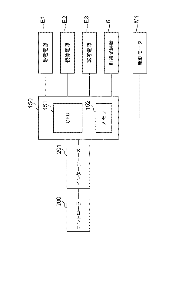
1.画像形成装置
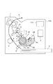
図1は、本発明の実施例1における画像形成装置100の概略構成図である。本実施例の画像形成装置100は、クリーナレス方式と接触帯電方式とを採用した電子写真方式のレーザビームプリンタである。
1. 1. Image forming apparatus FIG. 1 is a schematic configuration diagram of an
画像形成装置100は、回転可能な像担持体としてのドラム型(円筒形)の電子写真感光体である感光ドラム1を有する。画像出力動作が開始されると、感光ドラム1は、駆動源(駆動モータ)M1からの駆動が伝達されて図1の矢印R1方向に回転駆動される。回転する感光ドラム1の表面は、帯電手段としてのローラ型の帯電部材である帯電ローラ2によって、正規極性(本実施例では負極性)の所定の電位に一様に帯電処理される。帯電ローラ2は、導電性の弾性ローラであり、芯金のまわりに導電性弾性層を設けた構成である。図2に感光ドラム1と帯電ローラ2の構成配置図を示す。図2に示したように、帯電ローラ2は、感光ドラム1に接触して配置され、駆動源からの駆動力を受ける駆動力受け部材である帯電ローラ(駆動)ギア12によって駆動モータM1からの駆動が伝達されて図1の矢印R2方向に回転駆動される。本実施例の構成においては、感光ドラムフランジ11に設けられたギア部11aから帯電ローラギア12に駆動が伝達される構成となっている。本実施例における感光ドラム1と帯電ローラ2の駆動伝達方法を、図3を用いて説明する。メインモータである駆動モータM1から画像形成装置100側に配置された駆動ギア14に駆動が伝えられ、感光ドラム1に駆動が伝達されるように、カップリング部材13に駆動が伝達される。感光ドラム1が画像形成装置100に設置され、画像形成動作が開始される準備が整うと、カップリング部材13と感光ドラム1に設けられた感光ドラムフランジ11とが係合し、感光ドラム1が回転する。感光ドラムフランジ11に設けられたギア部11aと帯電ローラギア12は係合しているため、駆動モータM1からの駆動が帯電ローラギア12にも伝達される。したがって、帯電ローラ2も同時に回転駆動される構成となっている。このとき、帯電ローラ2には、図4に示した帯電電圧印加部としての帯電電源E1から、負極性の直流電圧である所定の帯電電圧が印加される。感光ドラム1と帯電ローラ2との接触部が帯電部aであり、感光ドラム1の回転方向において、感光ドラム1上の帯電ローラ2によって帯電処理される位置である。帯電ローラ2は、感光ドラム1の回転方向における帯電部aの上流側及び下流側の帯電ローラ2と感光ドラム1との間に形成される空隙(ギャップ)のうち少なくとも一方で生じる放電により、感光ドラム1の表面を帯電処理する。
The
帯電処理された感光ドラム1の表面は、露光手段(静電像形成手段)としてのレーザ露光ユニット3によって、画像データに応じて変調されたレーザビームLで走査露光される。露光ユニット3は、レーザビームLにより感光ドラム1の主走査方向(回転軸方向)に露光を繰り返しつつ、副走査方向(表面移動方向)にも露光を行うことで、感光ドラム1上に静電潜像を形成する。感光ドラム1の回転方向において、感光ドラム1上の露光ユニット3による露光位置が像露光部bである。
The surface of the charged
感光ドラム1上に形成された静電潜像は、現像手段としての現像ユニット4によって、現像剤としてのトナーを用いてトナー像として現像(可視化)される。現像ユニット4は、現像容器45と、回転自在に現像容器45に支持された現像部材(現像剤担持体)としての現像スリーブ41と、を有している。現像容器45には、現像剤としての磁性一成分現像剤であるブラックのトナーTが収容されている。本実施例のトナーTは、負帯電特性のものである。すなわち、本実施例では、トナーTの正規極性(現像時の帯電極性)は負極性である。現像スリーブ41は、現像容器45の感光ドラム1と対向する位置に設けられた開口部に、一部が外部に露出するようにして配置されている。現像スリーブ41は、アルミ素管に代表される中空の非磁性金属素管の周囲に、所定の体積抵抗を持つ導電性弾性ゴム層を設けたものである。現像スリーブ41の中空部には、磁界発生手段としてのマグネットローラ43が固定され配置されている。
The electrostatic latent image formed on the
現像容器45に収容されたトナーTは、撹拌部材44によって撹拌されると共に、マグネットローラ43の磁力により現像スリーブ41の表面に供給される。現像スリーブ41の表面に供給されたトナーTは、現像スリーブ41の回転に伴って現像剤規制手段としての現像ブレード42との対向部を通過することで、均一に薄層化され、摩擦帯電により負極性に帯電させられる。その後、現像スリーブ41上のトナーTは、現像スリーブ41の回転に伴って感光ドラム1と接触する現像位置まで搬送され、感光ドラム1上の静電潜像に応じて感光ドラム1に転移し、感光ドラム1上の静電潜像を現像する。このとき、現像スリーブ41には、図4に示した現像電圧印加部としての現像電源E2から、負極性の直流電圧である所定の現像電圧が印加される。本実施例では、イメージ部露光と反転現像により、トナー像が形成される。すなわち、一様に帯電処理された後に露光されることによって感光ドラム1の表面電位の絶対値が小さくなった露光領域(画像領域)に、感光ドラム1の帯電電位と同極性(本実施例では負極性)に帯電したトナーTが付着する。
The toner T contained in the developing
感光ドラム1の回転方向において、感光ドラム1上の現像スリーブ41と対向し、接触する位置が現像部cである。尚、本実施例では、現像スリーブ41は、現像部cにおいて感光ドラム1と現像スリーブ41との移動方向が同方向となるように、駆動モータM1によって図中矢印R3方向に回転駆動される。ここで、駆動源は、前述の駆動モータM1と共通としたが、別の駆動源を有してもよい。また、現像ユニット4は画像形成動作に合わせて感光ドラム1への接離の動作である当接離間動作を行う。この当接離間動作は、現像当接離間機構である当接離間カム46の動作によって行われる。当接離間カム46の回転により現像スリーブ41と感光ドラム1とを接触する当接位置と、接触しない離間位置とを、画像形成動作と非画像形成動作に合わせて移動する。
In the rotation direction of the
感光ドラム1上に形成されたトナー像は、感光ドラム1と、転写手段としてのローラ型の転写部材である転写ローラ5と、の接触部である転写部dに送られる。また、感光ドラム1上のトナー像とタイミングを合わせて、収容部8から搬送ローラ9などによって、被転写体である記録用紙などの記録材Pが、転写部dに搬送される。そして、感光ドラム1上のトナー像は、転写部dにおいて、転写ローラ5の作用により、感光ドラム1と転写ローラ5とに挟持されて搬送される記録材P上に転写される。このとき、転写ローラ5には、図4に示した転写電圧印加部としての転写電源E3から、トナーTの正規極性とは逆極性(本実施例では正極性)の直流電圧である所定の転写電圧が印加される。これにより、転写ローラ5と感光ドラム1との間に電界が形成され、感光ドラム1から記録材Pへとトナー像が静電的に転写される。
The toner image formed on the
トナー像が転写された記録材Pは、定着手段としての定着器7に送られる。定着器7において、記録材Pには熱及び圧力が加えられ、記録材Pに転写されたトナー像は記録材Pに定着される。
The recording material P to which the toner image is transferred is sent to the
ここで、画像形成装置100は、不図示の外部機器からの指示により開始される、単一又は複数の記録材Pに画像を形成する一連の画像出力動作(ジョブ)を行う。ジョブは、一般に、画像形成工程(印字工程)、前回転工程、複数の記録材Pに画像を形成する場合の紙間(記録材間)工程、及び後回転工程を有する。画像形成工程は、実際に感光ドラム1への静電潜像の形成、静電潜像の現像、トナー像の転写、トナー像の定着などを行う期間であり、より詳細には、帯電、露光、現像、転写、定着などの各工程が行われる位置により画像形成工程のタイミングは異なる。前回転工程は、画像形成工程の前の準備動作を行う期間である。紙間工程は、複数の記録材Pに対して画像形成工程を連続して行う際の、転写部dにおける記録材Pと記録材Pとの間に対応する期間である。言い換えると、連続印字時の、記録材Pが感光ドラム1と転写ローラ5の接触部dに介在しない期間である。後回転工程は、画像形成工程の後の整理動作(準備動作)を行う期間である。上記画像形成工程が画像形成動作であり、画像形成動作以外の動作期間(前回転工程、紙間工程、後回転工程など)が非画像形成動作である。そして、本実施例では、非画像形成動作の所定のタイミングで、帯電ローラ2に付着したトナーを感光ドラム1上に吐き出す清掃動作(帯電クリーニング動作)が実行される。
Here, the
続いて、本実施例における画像形成装置100の各構成について詳細に説明する。
Subsequently, each configuration of the
感光ドラム1は、OPC(有機光半導体)、アモルファスセレン、アモルファスシリコン等の感光材料を、アルミニウムやニッケルなどで形成されたφ24mmのシリンダ上のドラム基体上に設けて構成したものである。感光ドラム1は、画像形成装置100によって回転自在に支持されており、感光ドラムフランジ11によって図1に示す矢印R1方向に150mm/secのプロセススピードで回転駆動される。本実施の形態では、感光材料の厚さは15μmとした。
The
帯電ローラ2は導電性芯金と導電性ゴム層からなる単層ローラであって、外径φ7.5mm、体積抵抗103〜106Ω・cmである。また、導電性芯金には、負極性で直流の電圧(帯電バイアス)を印加可能な帯電電圧部としての帯電電源E1が接続されている。帯電ローラ2は帯電ローラギア12により駆動され、感光ドラム1の表面移動速度と速度差をもって回転している。ここで、帯電ローラ2を駆動させると、帯電ローラ2に付着するトナーを正規極性に帯電したトナーとなるように電荷を揃えることが出来るため、帯電ローラ2の汚れによる画像弊害を抑制することが出来る。
The charging
図4に示したように、露光ユニット3には、コントローラ200からインターフェース201を介して制御部150に入力し、画像処理された画像情報の時系列電気デジタル画素信号が入力する。露光ユニット3は、入力する時系列電気デジタル画素信号に対応して変調したレーザビームLを出力するレーザ出力部、回転多面鏡(ポリゴンミラー)、fθレンズ、反射鏡等を有しており、レーザビームLで感光ドラム1の表面を主走査露光する。この主走査露光と、感光ドラム1の回転による副走査により、画像情報に対応した静電潜像を形成する。
As shown in FIG. 4, the exposure unit 3 is input from the
転写ローラ5は導電性芯金と感光ドラム1への圧接部分が弾性体であるNBRヒドリンゴムを主成分とした導電性のスポンジ状のゴムからなり、外径が12.5mm、硬度30°(Asker−C,500gf荷重)のものを用いている。
The
2.クリーナレスシステム
以下に、本実施例における画像形成装置100のクリーナレスシステムについて説明する。図1の転写部dにおいて、記録材Pに転写されずに感光ドラム1上に残った転写残トナーは、帯電部aにおいて帯電電圧による電界によって放電し、感光ドラム1と同極性である負極性に帯電される。負極性に帯電した転写残トナーは、帯電部aにおいては感光ドラム1の表面電位と帯電電位との電位関係(感光ドラム1の表面電位=−700V、帯電電圧=−1300V)により、帯電ローラ2には付着せず通過する。帯電部aを通過した転写残トナーは、感光ドラム1の回転に伴い、像露光部bに送られる。転写残トナーは露光ユニット3のレーザビームLを遮蔽するほど多くはないため、感光ドラム1上の静電潜像を作像する工程に影響しない。その後、転写残トナーは現像部cに送られる。現像部cに送られてきたトナーは、非画像領域(非露光領域)では、感光ドラム1の表面の暗部電位Vd(−700V)と、現像電圧(−300V)との電位差により現像スリーブ41に転移し、現像ユニット4に回収される。現像ユニット4に回収されたトナーは、現像ユニット4内のトナーTと混合されて再利用される。
2. 2. Cleanerless system The cleanerless system of the
ここで、本実施の形態での現像電圧は、アース電位との電位差として表現される。したがって、現像電圧=−300Vは、アース電位(0V)に対して、現像スリーブ41の芯金に印加された現像電圧によって、−300Vの電位差を有したと解釈される。これは、帯電電圧や転写電圧に関しても同様である。
Here, the developing voltage in this embodiment is expressed as a potential difference from the ground potential. Therefore, it is interpreted that the developing voltage = −300V has a potential difference of −300V with respect to the ground potential (0V) due to the developing voltage applied to the core metal of the developing
一方、画像領域(露光領域)は、感光ドラム1の表面の明部電位Vl(−100V)と、現像電圧(−300V)との電位差により現像スリーブ41には転移せず、そのまま感光ドラム1上に残留する。そして、現像スリーブ41から感光ドラム1上に静電気的に供給されたトナーTと共に転写部dに送られ、画像として記録材Pに転写される。
On the other hand, the image region (exposure region) does not transfer to the developing
このように、画像形成装置100は、転写残トナーを現像と同時に現像ユニット4に回収する現像同時クリーニングを行っている。すなわち、現像ユニット4は、現像部cで感光ドラム1上の画像領域に現像ユニット4内のトナーTを供給する機能と、感光ドラム1上に残った転写残トナーを回収する機能とを兼ねている。
In this way, the
本実施例の画像形成装置100は、転写残トナーを帯電ローラ2に付着させずに通過させるために、以下の2つの構成を採用している。
The
第一は、図1に示したように、感光ドラム1の回転方向において転写部dより下流側かつ帯電部aより上流側に、感光ドラム1を除電処理する除電手段としての前露光ユニット6を設けていることである。前露光ユニット6は、帯電部aで安定した放電を生じさせるために、帯電部aに進入する前の感光ドラム1の表面を光除電する。感光ドラム1の回転方向において、転写部dより下流側かつ帯電部aより上流側の前露光ユニット6による露光位置が除電部eである。この前露光ユニット6により転写後の感光ドラム1を光除電し、帯電処理時に均一な放電を生じさせることによって、再び感光ドラム1上のトナーを正規極性に帯電させることが可能となる。
First, as shown in FIG. 1, a
第二は、本実施例における帯電ローラ2を、感光ドラム1に対して1.1倍の表面移動速度となるように周速差を設けて回転させていることである。この表面移動速度差によって、帯電ローラ2に付着した正極性に帯電したトナーを帯電部aで摺擦させて負極性に反転し、帯電ローラ2へのトナーの蓄積を抑制している。これら2つの構成により、帯電ローラ2へのトナー付着を抑制している。本実施例では、帯電ローラ2の長手一端に駆動力受け部材としての帯電ローラギア12が設けられており、帯電ローラギア12は感光ドラム1の同長手一端に設けられた感光ドラムフランジ11のギア部11aと係合している。よって、感光ドラム1の回転駆動に伴って、帯電ローラ2も回転駆動する。感光ドラム1と帯電ローラ2との間に周速差を設けることが出来る構成であれば、本実施例の構成に限らず採用することが出来る。例えば、感光ドラム1と帯電ローラ2を回転させるための駆動源(駆動モータ)を独立で有し、それぞれの駆動源から駆動を入力させて回転させてもよい。
The second is that the charging
3.制御態様
続いて、本実施例における制御態様について説明する。
3. 3. Control mode Next, the control mode in this embodiment will be described.
制御部150は画像形成装置100の動作を制御する手段であり、各種の電気的情報信号の授受をする。また、各種のプロセス機器やセンサから入力する電気的情報信号の処理、各種のプロセス機器への指令信号の処理を行う。図4は、本実施例における画像形成装置100の要部の概略制御態様を示すブロック図である。コントローラ200は、ホスト装置との間で各種の電気的な情報の授受をすると共に、画像形成装置100の画像形成動作を所定の制御プログラムや参照テーブルに従って、インターフェース201を介して制御部150で統括的に制御する。
The
画像形成装置100に設けられた制御手段としての制御部150は、演算処理を行う中心的素子であるCPU151、記憶素子であるROM、RAMなどのメモリ152などを有して構成される。RAMには、センサの検知結果、演算結果などが格納され、ROMには制御プログラム、予め求められたデータテーブルなどが格納されている。制御部150は、画像形成装置100の動作を統括的に制御する制御手段であり、各種の電気的情報信号の授受や、駆動のタイミングなどを制御しており、所定の作像シーケンス制御などを司る。制御部150には、画像形成装置100における各制御対象が接続されている。例えば、制御部150には、帯電電源E1、現像電源E2、転写電源E3、前露光ユニット6、駆動モータM1などが接続されている。特に、本実施例との関係で言えば、制御部150は、各種電源E1、E2、E3のON/OFFや出力値、前露光ユニット6による除電光の照射のON/OFF、駆動モータM1のON/OFFなどを制御して、後述する帯電クリーニング動作を実行させる。
The
そして、この画像形成装置100は、ホスト装置からコントローラ200に入力される電気的画像信号に基づいて、記録材Pに画像形成を行う。なお、ホスト装置としては、イメージリーダー、パソコン、ファクシミリ、スマートフォン等が挙げられる。
Then, the
4.注入帯電
次に、注入帯電について説明する。なお、以下の説明において、電圧値、電流値、電位の大小関係について言及する場合は、便宜上、その絶対値についての大小関係を言うものとする。
4. Injection charging Next, injection charging will be described. In the following description, when the magnitude relation of the voltage value, the current value, and the potential is referred to, the magnitude relation of the absolute value is referred to for convenience.
注入帯電は、感光ドラム1と帯電ローラ2のような電圧が印加された部材とが当接して回転する際に感光ドラム1の表面上に電位が形成される現象である。感光ドラムと部材との間のギャップによって生じる放電での電位形成とは別に、部材から感光ドラム1に電荷が移動することにより電流が流れ、感光ドラム1の表面に電位が形成される。注入帯電が生じる例として、電圧が印加された部材である帯電ローラ2と感光ドラム1が当接し、お互いの表面移動速度が異なる状態で回転する本実施例のような場合や、感光ドラム1の表面の抵抗が低い場合などがある。
Injection charging is a phenomenon in which an electric potential is formed on the surface of the
本実施例では、感光ドラム1の表面移動速度に対して帯電ローラ2の表面移動速度(周速比)を110%としている。これにより、回転によって感光ドラム1の表面と帯電ローラ2の表面が摺擦される。感光ドラム1の表面移動速度に対して帯電ローラ2の表面移動速度を105%以上120%以下とすることで、逆極性に帯電したトナー付着を抑制し、感光ドラム1の表面への注入帯電を抑制することが出来るため好ましい。
In this embodiment, the surface moving speed (peripheral speed ratio) of the charging
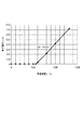
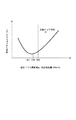
表面の摺擦による感光ドラム1への電位形成の影響を、図5を用いて説明する。図5は、帯電ローラ2に−100Vの帯電電圧を印加し、表面電位が0Vの感光ドラム1に対してそれぞれの周速比を有した状態で回転させた時の感光ドラム1の表面電位の上昇量をプロットしたものである。図5から分かるように、感光ドラム1と帯電ローラ2の周速比が大きいと、感光ドラム1の表面電位上昇量が大きくなる。感光ドラム1の表面電位の上昇が生じるのは帯電ローラ2からの電荷の移動によるためである。したがって、周速比が大きいと、感光ドラム1の表面と帯電ローラ2の表面との実質の接触面積が大きくなるため、感光ドラム1の表面に帯電ローラ2から電荷が移動する機会が増える。したがって、周速比は感光ドラム1の表面電位上昇量に依存性があり、大きいほど表面電位が上昇するということになる。
The effect of potential formation on the
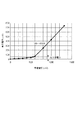
図6、図7は、帯電ローラ2に印加した帯電電圧と感光ドラム1の表面電位との関係を、温度30℃、相対湿度80%の高温高湿(H/H)環境で測定した結果を示すグラフ図である。なお、図6は、感光ドラム1と帯電ローラ2との周速比が100%であり、感光ドラム1に帯電ローラ2が従動する場合の測定結果を示している。一方、図7は、本実施例の構成である感光ドラム1と帯電ローラ2との周速比が110%の場合の測定結果を示している。H/H環境で測定することにより、感光ドラム1の表面抵抗が下がるため、注入帯電が発生しやすくなる。
6 and 7 show the results of measuring the relationship between the charging voltage applied to the charging
図6は、帯電ローラ2に印加する直流電圧を大きくしていくと、ある電圧値までは感光ドラム1の表面電位に変化はないが、ある電圧値から感光ドラム1の表面電位が上昇し始める。この感光ドラム1の表面電位が上昇し始める直流電圧の値が、放電開始電圧Vthである。本実施例では、放電開始電圧Vthは、一例として−550Vであるものとする。なお、放電開始電圧Vthは、帯電ローラ2と感光ドラム1との間のギャップ、感光ドラム1の感光体層の厚み、感光ドラム1の感光体層の比誘電率などによって決まる。放電開始電圧Vth以上の直流電圧を帯電ローラ2に印加すると、パッシェンの法則に基づき、帯電ローラ2と感光ドラム1との間のギャップでの放電現象が発生し、感光ドラム1の表面に電荷が載り、電位が形成される。つまり、帯電ローラ2に放電開始電圧Vth以上の直流電圧を印加した場合に、感光ドラム1の表面電位は上昇を開始し、それ以降は帯電ローラ2に印加する直流電圧に対して略傾き1の線形の関係にて感光ドラム1の表面電位が上昇する。したがって、電子写真に必要とされる感光ドラム1の表面電位Vdを得るためには、直流電圧Vd+Vthを帯電ローラ2に印加することが必要である。直流電圧Vd+Vthを帯電ローラ2に印加すると、感光ドラム1と帯電ローラ2との間で放電が起こり、直流電圧Vd分だけ感光ドラム1の表面上に電位が形成される。
In FIG. 6, when the DC voltage applied to the charging
一方、図7は、周速比110%で回転させることにより、帯電ローラ2に印加する直流電圧が放電開始電圧Vthよりも低い場合にも、感光ドラム1の表面電位が上昇し始める。そして、帯電ローラ2に放電開始電圧Vthを印加すると、感光ドラム1の表面電位は約−50Vとなる。これは、感光ドラム1の表面の電気抵抗の低下に加え、摺擦によって電荷が移動して注入帯電が発生し、パッシェンの法則に基づく放電開始電圧Vth未満の直流電圧を印加した場合にも、感光ドラム1の表面に微小な電位が形成されることによる。
On the other hand, in FIG. 7, the surface potential of the
上記記載の条件の他、感光ドラム1の表面抵抗が下がる条件として、放電生成物が感光ドラム1の表面に付着した場合や、抵抗が低い外添剤や異物が付着した場合なども同じような現象が生じる。放電生成物とは、感光ドラム1と帯電ローラ2とが当接した帯電部aのギャップで放電が起こることにより、オゾンやNOx等が反応により発生して生成される物質である。この放電生成物は、H/H環境のように空気中の絶対水分量が大きい環境において、感光ドラム1の表面上で水分を吸着し、抵抗を下げる傾向がある。放電生成物が感光ドラム1に付着すると、帯電ローラ2と感光ドラム1との間に表面移動速度差が無い従動の構成であっても注入帯電が発生する。以上説明したような、放電生成物などの物質が付着した場合においても、本実施例の構成を適応させてもよい。
In addition to the above-mentioned conditions, the conditions for lowering the surface resistance of the
5.帯電クリーニング動作
本実施例では、画像形成装置100の不図示の環境センサとしての検知部によって、温度27℃/湿度70%以上を検知した場合はH/H環境と判断し、非画像形成動作時に行う帯電クリーニング動作の電圧制御を可変としている。尚、H/H環境の判断基準は、感光ドラム1や帯電ローラ2の材質等に応じて適宜変更可能であるものの、環境センサで検知した温度と湿度から算出された空気中の絶対水分量が15.0g/m3以上であることが望ましい。
5. Charged cleaning operation In this embodiment, when the detection unit as an environmental sensor (not shown) of the
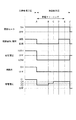
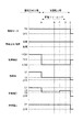
図8は、本実施例のH/H環境における帯電クリーニング動作のタイミングチャートを示している。帯電クリーニング動作は、制御部150により図8に示すタイミングで各部の動作が制御される。さらに、本実施例では、画像出力枚数が所定の閾値以上となる毎に、後回転工程において清掃動作としての帯電クリーニング動作が実行される。以下、帯電クリーニング動作の詳細について説明する。
FIG. 8 shows a timing chart of the charge cleaning operation in the H / H environment of this embodiment. In the charge cleaning operation, the
画像形成工程が終了し、記録材Pが転写部dを抜けたタイミング(A)から後回転工程に入る。このタイミング(A)で、制御部150は現像スリーブ41の当接離間カム46を回転させて現像スリーブ41を感光ドラム1から離間させる。これは、現像スリーブ41から感光ドラム1上に転移するかぶりトナーを抑制し、帯電クリーニングを充分に行うためである。かぶりトナーとは、感光ドラム1の非画像形成部に付着するトナーの総称であり、感光ドラム1の暗部電位Vdと現像スリーブ41に印加する現像電圧の電位差であるバックコントラスト(Vback)の大きさによって付着量が決まるものである。そして、同タイミング(A)で、転写ローラ5に印加する転写電圧をHIGH(+1000V)からLOW(−1000V)に切り替える。転写電圧をLOW(−1000V)に切り替えることで、感光ドラム1の暗部電位Vd(−700V)よりも負極性側にすることにより、転写ローラ5から感光ドラム1への正電荷の流入を防止している。これにより、感光ドラム1上のトナーTへの正電荷の流入もなくなり、転写電圧による感光ドラム1上のトナーの正極性化を抑制する。本実施例においては、転写ローラ5は感光ドラム1の回転に従動する構成を有している。しかし、転写ローラ5を駆動形式にした場合には、転写ローラ5から感光ドラム1への電流の流れ込みによる注入帯電での表面電位の形成も抑止するために、転写電圧を制御してもよい。具体的には、転写電圧LOWを−700Vに設定し、感光ドラム1の表面電位と略同電位としてもよい。また、同タイミング(A)で、帯電ローラ2に印加する帯電電圧を、画像形成中の帯電電圧C1(−1300V)から帯電クリーニング用の帯電電圧C2(−800V)に切り替える。この帯電電圧を帯電クリーニング用の電圧に切り替えるタイミングを、帯電クリーニング動作の開始タイミングとする。さらに、同タイミング(A)で、前露光ユニット6をOFFにする。これにより、感光ドラム1の表面電位の絶対値を小さくすることなく帯電ローラ2からの放電をなくすことによって、帯電ローラ2上のトナーの正極性化を抑制する。
The image forming step is completed, and the back rotation step is started from the timing (A) when the recording material P passes through the transfer portion d. At this timing (A), the
転写ローラ5及び帯電ローラ2においてトナーの正極性化を抑制し、且つ感光ドラム1と帯電ローラ2との摺擦によってトナーを正規極性である負極性に帯電させる。そして、感光ドラム1の表面電位(−700V)と帯電電圧C2(−800V)との電位差Δによって、正規極性に帯電したトナーを感光ドラム1へと転移させる。しかし、H/H環境下で、前露光ユニット6をOFFした状態で帯電電圧を印加し続けた場合、感光ドラム1の表面電位が帯電電圧からの注入帯電により上昇し、帯電ローラ2の表面電位である帯電電圧C2に近づく。
The
そこで、帯電電圧を帯電電圧C2(−800V)に切り替えたタイミング(A)から、感光ドラム1が約2周分回転したタイミング(B)で、帯電電圧を帯電クリーニング動作開始時の帯電電圧C2(−800V)から帯電電圧C3(−850V)に切り替える。これは、帯電ローラ2の表面電位を感光ドラム1の表面電位に対して負極性側に大きい状態を維持するためである。したがって、帯電電圧を切り替えるタイミング(B)は上記タイミングに限らず、帯電ローラ2の表面電位が感光ドラム1の表面電位に対して負極性側に大きい状態を維持できればよい。そのためには、帯電電圧の変更幅も50Vに限らず、感光ドラム1の表面電位の変化量に応じて可変としてもよい。
Therefore, the charging voltage is changed from the timing (A) when the charging voltage is switched to the charging voltage C2 (-800V) to the timing (B) when the
さらに、帯電電圧を帯電電圧C3(−850V)に切り替えたタイミング(B)から感光ドラム1が約1周分回転したタイミング(C)で、帯電電圧を帯電電圧C3(−850V)から帯電電圧C4(−900V)に切り替える。これも同様に、帯電ローラ2の表面電位を感光ドラム1の表面電位に対して負極性側に大きくするためであり、帯電電圧C3(−850V)の帯電電圧を受けた帯電部aが感光ドラム1を1周したときには、さらに絶対値が大きい帯電電圧が必要となる。したがって、タイミング(C)は上記タイミングに限らず、帯電ローラ2の表面電位が感光ドラム1の表面電位に対して負極性側に大きい状態を維持できればよい。そのためには、帯電電圧の変更幅を50Vに限らず、感光ドラム1の表面電位の変化量に応じて可変としてもよい。
Further, the charging voltage is changed from the charging voltage C3 (-850V) to the charging voltage C4 at the timing (C) when the
次に、帯電電圧を帯電電圧C4(−900V)に切り替えたタイミング(C)から感光ドラム1が約1周分回転したタイミング(D)で、現像スリーブ41を感光ドラム1と再び当接させる。これにより、感光ドラム1上の正規極性である負極性に帯電したトナーは、現像部cにおいて、感光ドラム1の表面電位と現像電圧との電位差により現像スリーブ41に転移し、現像ユニット4に回収される。感光ドラム1は全周にわたり正規極性である負極性トナーが存在しているため、現像回収時間は少なくとも感光ドラム1の1周以上必要である。
Next, the developing
本実施例においては、帯電電圧を帯電電圧C4に切り替えた後、現像スリーブ41が感光ドラム1に当接してから感光ドラム1が1周回転したタイミング(E)で帯電クリーニング動作を終了する。すなわち、図8のタイミング(A)からタイミング(E)が帯電クリーニング動作期間であり、本実施例における帯電クリーニングの時間は2.0sである。この時間は、帯電ローラ2の回転数で約12周分であり、この程度摺擦させることによって帯電ローラ2上のトナーTは充分に負極性に帯電され、感光ドラム1へと転移する。尚、帯電クリーニング時間は、帯電ローラ2と感光ドラム1との表面移動速度差や付着しているトナーの状態等によって適宜変更可能である。
In this embodiment, after switching the charging voltage to the charging voltage C4, the charging cleaning operation is completed at the timing (E) when the developing
帯電クリーニング動作が終了したタイミング(E)以降は、現像スリーブ41の離間動作、或いは各種電圧のOFF、駆動モータM1のOFFといった制御がタイミング(Z)にて行われ、一連の画像出力動作が終了する。
After the timing (E) when the charge cleaning operation is completed, control such as the separation operation of the developing
本実施例においては、感光ドラム1の表面電位Vd(−700V)に対して、帯電クリーニング用の帯電電圧C2を−800Vに設定し、電位差Δを100Vとしたが、これに限らず、電位差Δを大きくしてもよい。電位差Δを大きくすると、感光ドラム1の回転1周目のクリーニング性能は高い。しかし、電位差Δが大きい分、感光ドラム1に作用する注入帯電量も多くなるため、帯電電圧C3、C4の大きさも大きく設定しなければならない。したがって、感光ドラム1の回転数が多くなるほど帯電電圧の絶対値を本実施例以上に大きくする必要がある。
In this embodiment, the charging voltage C2 for charging cleaning is set to -800V and the potential difference Δ is set to 100V with respect to the surface potential Vd (-700V) of the
6.帯電クリーニング動作における注入帯電の影響による帯電電圧制御の効果
次に、帯電クリーニング動作時に帯電電圧制御を行うことによる効果確認を行った。帯電電圧−1300Vで画像形成を開始し、2枚間欠動作によって、印字率10%の画像を5000枚印字したときの、画像弊害を確認した。
6. Effect of charge voltage control due to the influence of injection charging in the charge cleaning operation Next, the effect of performing charge voltage control during the charge cleaning operation was confirmed. Image formation was started at a charging voltage of -1300 V, and an image adverse effect was confirmed when 5000 images with a printing rate of 10% were printed by intermittent operation of two images.
実施例1としては、間欠動作ごとに実行される帯電クリーニング動作において図8に示したような帯電電圧の補正制御を行った。一方、比較例1では、帯電電圧の補正を行わず、画像形成時と同じ帯電電圧で帯電クリーニング動作を行った。表1に画像形成枚数に応じた画像弊害の結果を示す。 In the first embodiment, the correction control of the charging voltage as shown in FIG. 8 was performed in the charging cleaning operation executed for each intermittent operation. On the other hand, in Comparative Example 1, the charging cleaning operation was performed at the same charging voltage as at the time of image formation without correcting the charging voltage. Table 1 shows the results of image harmful effects according to the number of images formed.
表中の〇は記録材P上で、画像弊害が発生していない状態を示し、×は記録材P上にかぶりトナーや縦スジ、ポチなどが視認され画像弊害が発生している状態を示している。 In the table, ◯ indicates a state in which no image harmful effect has occurred on the recording material P, and × indicates a state in which fog toner, vertical streaks, spots, etc. are visually recognized on the recording material P and an image harmful effect has occurred. ing.
比較例1に関しては、画像形成枚数が3000枚で画像弊害が発生した。これは、帯電クリーニング動作時の帯電電圧を補正せずに帯電クリーニング動作を実行した事によって、帯電ローラ2から感光ドラム1への正規極性に帯電したトナーの転移が十分に行われなかったことが原因であると考えられる。つまり、注入帯電によって感光ドラム1の表面電位の絶対値が上昇し、帯電ローラ2と感光ドラム1の表面電位の電位差Δが小さくなってしまったということである。
Regarding Comparative Example 1, the number of images formed was 3000, which caused an adverse image effect. This is because the charging cleaning operation was performed without correcting the charging voltage during the charging cleaning operation, so that the toner charged to the normal polarity was not sufficiently transferred from the charging
一方、実施例1では、画像弊害は終始視認できないレベルとなった。帯電クリーニング動作中の感光ドラム1の回転に応じて帯電電圧制御を行い、適切なタイミングで帯電電圧の値を変化させたことによって、摺擦による注入電位分の上昇をキャンセルする事が出来たためであると考えられる。以上の動作を行ったことにより、帯電クリーニング動作中において、感光ドラム1の表面電位と帯電ローラ2との電位差Δを保持することが出来た。
On the other hand, in Example 1, the harmful effects of the image were at a level that could not be visually recognized from beginning to end. By controlling the charging voltage according to the rotation of the
本実施例では、帯電ローラ2から感光ドラム1に電荷が注入される注入帯電が生じる画像形成装置100において、以下のような特徴を備えた画像形成装置100を用いた。制御部150は、記録材Pにトナー像を形成する画像形成動作と、帯電ローラ2に付着したトナーを感光ドラム1に転移させて現像スリーブ41に回収して帯電ローラ2を清掃する帯電クリーニング動作と、を実行するように制御する。そして、帯電クリーニング動作において、正規極性に帯電したトナーに帯電ローラ2から感光ドラム1に向かう方向の静電気力が作用する向きの電位差Δが形成されるように帯電ローラ2に印加する第1の帯電電圧を以下のように制御する。第1の帯電電圧を印加した後に、第1の帯電電圧より絶対値が大きい第2の帯電電圧を帯電ローラ2に印加するように帯電電圧を切り替える。このように制御することにより上記効果を得ることが出来る。
In this embodiment, in the
以上説明したように、本実施例によれば、後回転工程の帯電クリーニング動作の期間において、帯電電圧を負極性側に段階的に大きくなるように切り替える。段階的に大きくするタイミングは、感光ドラム1の回転1周毎のタイミングとすると、注入した感光ドラム1に対して帯電電圧を上げた状態となる。これにより、帯電ローラ2の表面電位を感光ドラム1の表面電位に対して負極性側に大きい状態を維持することができ、負極性トナーを感光ドラム1へ転移させるための必要な電界を得ることができる。よって、帯電ローラ2へのトナーの蓄積を抑制し、縦スジやポチ等の画像不良のない良好な画像を提供することができる。
As described above, according to the present embodiment, during the period of the charge cleaning operation in the post-rotation step, the charge voltage is switched to gradually increase toward the negative electrode side. Assuming that the timing of stepwise increase is the timing for each rotation of the
尚、本実施例において、現像スリーブ41の離間動作開始タイミングと、帯電電圧、転写電圧の切り替えタイミングを同じタイミング(A)としているものの、これに限らない。例えば、現像スリーブ41が感光ドラム1から完全に離間するまでに帯電部aに帯電電圧が印加されていればよい。また、転写電圧がLOWに切り替わる前に転写ローラ5から吐き出されたトナーが帯電部aを通過してから帯電電圧を切り替えてもよい。
In this embodiment, the timing for starting the separation operation of the developing
また、本実施例における前露光ユニット6は、光を直接感光ドラム1の除電部eに照射する構成としているが、これに限定されるものではなく、例えばファーブラシのように、導電性の繊維からなるブラシ部材の毛先を感光ドラム1に当接させる構成でもよい。また、ライトガイドなど照射角がある場合は、適宜、前露光ユニット6をON/OFFするタイミングを変更してもよい。
Further, the
また、本実施例における帯電部材はローラ状の部材であるものとして説明したが、これに限定されるものではない。例えば、複数の支持ローラに巻回された無端ベルト状の帯電部材でもよい。例えば、複数の支持ローラのうちの一つがベルトを介して感光ドラムに当接したものなど、他の形態の回転部材も好適に用いてもよい。 Further, although the charging member in this embodiment has been described as being a roller-shaped member, the present invention is not limited to this. For example, an endless belt-shaped charging member wound around a plurality of support rollers may be used. For example, other forms of rotating members, such as one in which one of the plurality of support rollers is in contact with the photosensitive drum via a belt, may be preferably used.
また、本実施例における帯電クリーニング動作は、非画像形成時としての後回転工程において実行されるものとして説明したが、これに限定されるものではなく、非画像形成時であれば任意のタイミングで実行してもよい。例えば、印字工程のジョブ中に画像出力枚数が所定の閾値以上になった場合に、紙間を延長するなどして帯電クリーニング動作を実行することもできる。さらに、本実施例におけるクリーニング動作は、環境センサとしての検知部によってH/H環境と検知された場合に限定したが、その他の環境においても適用できるものとする。 Further, the charge cleaning operation in this embodiment has been described as being executed in the post-rotation step as the non-image formation, but the present invention is not limited to this, and the charge cleaning operation is not limited to this, and can be performed at any timing during the non-image formation. You may do it. For example, when the number of image output sheets exceeds a predetermined threshold value during a job in the printing process, it is possible to execute a charge cleaning operation by extending the space between papers. Further, the cleaning operation in this embodiment is limited to the case where the detection unit as the environment sensor detects the H / H environment, but it can be applied to other environments as well.
また、図9に示すように、帯電クリーニング動作を実行する後回転工程開始時の帯電電圧を画像形成動作である画像形成工程から変更せずに、そのまま段階的に上げる(帯電電圧C7、帯電電圧C8に変更する)ような制御を行ってもよい。但し、その場合は、現像回収時に感光ドラム1の表面電位と現像電圧との電位差であるバックコントラスト(Vback)を安定させるために、感光ドラム1の表面電位の絶対値を下げるか、或いは現像電圧の絶対値を上げるといった制御が必要となる。
Further, as shown in FIG. 9, the charging voltage at the start of the post-rotation process after executing the charging cleaning operation is increased stepwise as it is without changing from the image forming process which is the image forming operation (charging voltage C7, charging voltage). Control such as (change to C8) may be performed. However, in that case, in order to stabilize the back contrast (Vback), which is the potential difference between the surface potential of the
また、図10に示すように、帯電クリーニング用の帯電電圧C2から帯電電圧C4に向けて線形に上げるような制御を行ってもよい。 Further, as shown in FIG. 10, control may be performed so as to linearly increase the charging voltage C2 for charging cleaning toward the charging voltage C4.
また、本実施例では、現像剤としての磁性一成分現像剤であるトナーを用いたが、非磁性一成分現像剤であってもよい。 Further, in this embodiment, toner which is a magnetic one-component developer is used as a developer, but a non-magnetic one-component developer may be used.
また、本実施例では、単一の感光ドラム1と帯電ローラ2と現像ユニット4などにより構成される単一のカートリッジ構成を有する画像形成装置100を用いたが、複数のカートリッジ構成を有する画像形成装置に適応させてもよい。例えば、感光ドラム1から中間転写体たる中間転写ベルトにトナー像を転写させてから記録材に転写させる中間転写方式を用いてもよい。
Further, in this embodiment, the
[変形例1]
本変形例で適用する画像形成装置100の構成において、実施例1と同一部材には同一符号とし、説明を省略する。
[Modification 1]
In the configuration of the
本変形例は、実施例1と同じ構成を持つ画像形成装置100において、帯電ローラ2のクリーニング部材としての帯電ローラブラシ21が設けられていることを特徴としている。図11は、本変形例における画像形成装置100の概略構成図である。帯電ローラブラシ21は、帯電ローラ2に対して所定の圧力がかかるように取り付けられている。帯電ローラブラシ21は導電性を有し、帯電ローラ2と同電位の電圧が印加することで、摩擦帯電により帯電ローラ2上のトナーを負極性にしている。帯電ローラ2上の負極性トナーは感光ドラム1との接触部である帯電部aに到達すると、静電的に感光ドラム1に転移するため、帯電ローラ2のクリーニングを行うことが出来る。帯電ローラ2のクリーニング性の観点から、帯電ローラブラシ21と帯電ローラ2との間に電位差を設けてもよい。
This modification is characterized in that, in the
上述した帯電ローラブラシ21を設けた画像形成装置100において、例えば、連続して画像形成を行った場合に、帯電ローラブラシ21にトナーが溜まる。帯電ローラブラシ21にトナーが溜まると、帯電ローラ2のクリーニング性能が低下し、帯電ローラ2のトナー付着量が増えて帯電性能の低下による画像不良が発生する。そこで、本変形例における帯電クリーニング動作では、帯電ローラブラシ21に溜まったトナーを帯電ローラ2に吐き出すための時間が必要となる。
In the
2.帯電クリーニング動作
図12は、本変形例における帯電クリーニング動作のタイミングチャートを示している。図12において、タイミング(A)からタイミング(C)までは実施例1と同様のため説明を割愛する。本変形例においては、さらに、帯電電圧C4に切り替えたタイミング(C)から、感光ドラム1が約1周分回転したタイミング(D)で、帯電電圧C4(−900V)から帯電電圧C5(−950V)に切り替える。また、帯電電圧C5に切り替えたタイミング(D)から、感光ドラム1が約1周分回転したタイミング(E)で、帯電電圧C5から帯電電圧C6(−1000V)に切り替える。これらも同様に、帯電ローラ2の表面電位を感光ドラム1の表面電位に対して負極性側に大きい状態を維持するためである。実施例1の図8に示した帯電クリーニング動作に比べて、タイミング(D)、(E)の分だけ延長させていることにより、帯電ローラブラシ21から帯電ローラ2にトナーを転移させる時間を稼いでいる。タイミング(D)及びタイミング(E)は上記タイミングに限らず、帯電ローラ2の表面電位が感光ドラム1の表面電位に対して負極性側に大きい状態を維持できればよい。また、そのためには、帯電電圧の変更幅も50Vに限らず、感光ドラム1の表面電位の変化量に応じて可変としてもよい。
2. 2. Charge cleaning operation FIG. 12 shows a timing chart of the charge cleaning operation in this modified example. In FIG. 12, since the timing (A) to the timing (C) are the same as those in the first embodiment, the description thereof will be omitted. In this modification, the charging voltage C4 (-900V) to the charging voltage C5 (-950V) are further changed from the timing (C) when the
次に、帯電電圧C6に切り替えたタイミング(E)から、感光ドラム1が約1周分回転したタイミング(F)で、現像スリーブ41を感光ドラム1と再び当接させる。これにより、感光ドラム1上の負極性トナーは、現像部cにおいて、感光ドラム1の表面電位と現像電圧との電位差により、現像スリーブ41に転移し、現像ユニット4に回収される。
Next, the developing
本変形例も同様に、現像スリーブ41が感光ドラム1に当接してから感光ドラム1が1周回転したタイミング(G)で帯電クリーニング動作を終了する。すなわち、図12のタイミング(A)からタイミング(G)が帯電クリーニング動作期間であり、本変形例における帯電クリーニング動作の時間は2.8sである。この期間は、帯電ローラ2の回転数で約18周分であり、帯電ローラブラシ21に溜まったトナーを充分に帯電ローラ2に吐き出すと共に、帯電ローラ2上のトナーを負極性に帯電させて感光ドラム1へと転移することができる。尚、帯電クリーニング動作時間は、帯電ローラ2と感光ドラム1との周速比や付着しているトナーの状態等によって適宜変更可能である。
Similarly, in this modification, the charge cleaning operation is completed at the timing (G) when the
帯電クリーニング動作が終了したタイミング(F)以降は、実施例1と同様であり、タイミング(G)までの500msは現像スリーブ41による負極性トナーの回収時間である。そして、タイミング(G)以降の後回転工程において、タイミング(Z)で現像スリーブ41の離間動作や各種電圧、駆動モータM1のOFFといった制御が制御部150にて行われ、一連の画像出力動作が終了する。
After the timing (F) when the charge cleaning operation is completed, the same as in the first embodiment, and 500 ms until the timing (G) is the recovery time of the negative electrode toner by the developing
本変形例のような、帯電ローラ2のクリーニング部材としての帯電ローラブラシ21を設けた場合においても、帯電クリーニング動作時間を延長することにより、実施例1と同様の作用効果が得られる。帯電ローラブラシ21からトナーを吐き出す時間を延長した分の回転中、帯電電圧の絶対値をさらに段階的に上げることによって感光ドラム1への注入帯電の影響をキャンセルすることが可能となる。
Even when the charging
[変形例2]
本変形例で適用する画像形成装置100の構成において、実施例1と同一部材には同一符号とし、説明を省略する。
[Modification 2]
In the configuration of the
本変形例は、実施例1と同じ構成を持つ画像形成装置100において、感光ドラム1のクリーニング部材としてのクリーニングブレード22が設けられていることを特徴としている。図13は、本変形例における画像形成装置100の概略構成図である。クリーニングブレード22はウレタンゴムから形成されており、感光ドラム1の表面に所定の圧力で圧接されている。感光ドラム1上の転写残トナーは、クリーニングブレード22によってかき落とされ、クリーニング容器23に収容される。
This modification is characterized in that the
上述したクリーニングブレード22を設けた画像形成装置100においても、帯電ローラ2にトナーが付着する。例えば、クリーニングブレード22に突入するトナーが多い場合や、連続して画像形成を行った場合などは、クリーニングブレード22によってクリーニングされるべきトナーがすり抜けることがある。特に、クリーニングブレード22の使用の累積に伴いクリーニング能力が低下した場合は、より多くのトナーが帯電ローラ2に付着する。そこで、本変形例においては、感光ドラム1、クリーニングブレード22の使用の累積に応じて帯電クリーニング動作の電圧制御を行い、帯電電圧を可変としている。そのために、本変形例の画像形成装置100には、感光ドラム1の使用状況を示した積算回転数の情報を書き込んだ不図示の不揮発性記録媒体(メモリ)を有している。本変形例では、不図示の環境センサがH/H環境であると判断し、且つ積算回転数が感光ドラム1の寿命の50%を超えた以降に、実施例1と同様の帯電クリーニング動作を実施する。尚、帯電クリーニング動作を実施するタイミングは、感光ドラム1の寿命の50%に限ることはない。
Even in the
帯電クリーニング動作は実施例1と同様のため、詳細な説明を割愛する。 Since the charge cleaning operation is the same as that of the first embodiment, detailed description thereof will be omitted.
本変形例のような、感光ドラム1のクリーニング部材としてのクリーニングブレード22を設けた場合においても、実施例1と同様の作用効果が得られる。さらに、帯電ローラ2のトナーの付着具合に応じて帯電電圧を制御することによって、ダウンタイムを無駄に増やすことなく好適に帯電クリーニング動作を実行することが出来る。
Even when the cleaning blade 22 as a cleaning member of the
[実施例2]
本実施例で適用する画像形成装置100の構成において、実施例1と同一部材には同一符号とし、説明を省略する。
[Example 2]
In the configuration of the
本実施例における画像形成装置100は、現像スリーブ41を感光ドラム1に対して当接離間できる離間機構46を設けていない。これにより、離間機構のカム46など部品削減によるコストダウンや画像形成装置100の小型化が図れる。また、帯電クリーニング動作において、帯電電圧の変更に同期して現像電圧を変更することが大きな特徴である。本実施例の画像形成装置100は、離間機構のカム46が配置されないこと以外は図1と同じ概略構成図である。
The
1.帯電クリーニング動作
図14は、本実施例における帯電クリーニング動作のタイミングチャートを示している。本実施例では、現像スリーブ41と感光ドラム1が当接した状態で帯電クリーニング動作が行われる。実施例1と同様に、画像形成動作が終了し、記録材Pが転写部dを抜けたタイミング(A)から帯電クリーニング動作を実行する後回転工程に入る。このタイミングで、帯電ローラ2に印加する帯電電圧を、画像形成中の帯電電圧C1(−1300V)から帯電クリーニング用の帯電電圧C2(−800V)に切り替える。この帯電電圧の切り替えタイミング(A)が帯電クリーニング動作の開始タイミングである。また、同タイミング(A)で、前露光ユニット6をOFFする。さらに、同タイミング(A)で、転写ローラ5に印加する転写電圧をHIGH(+1000V)からLOW(−1000V)に切り替える。
1. 1. Charge cleaning operation FIG. 14 shows a timing chart of the charge cleaning operation in this embodiment. In this embodiment, the charge cleaning operation is performed with the developing
前露光ユニット6をOFFした後は、感光ドラム1の表面電位は帯電電圧からの注入帯電によって、帯電電圧C2(−800V)に近づく。これに伴い、感光ドラム1の表面電位と現像電圧D1(−300V)との間の電位差であるVbackは、概ね400Vから500Vの間になる。
After turning off the
図15に、本実施例における感光ドラム1の表面電位と現像電圧の電位差であるVbackと感光ドラム1の表面上に付着するかぶりトナー量の関係を示した。かぶりトナー量は、感光ドラム1上のトナーをマイラーテープでテーピングして写し取り、基準紙上にテープを張り付けた後に、その濃度を東京電色社の反射濃度計(TC−6DS/A)で測定した。かぶりトナー量の算出方法は、画像形成装置100を用いて画像形成動作を行い、記録材Pを使わずにVbackを変化させて現像させたときの、感光ドラム1上のトナー量から算出を行った。図15に示すように、Vbackが400Vから500Vの間は、感光ドラム1上のかぶりトナーの量は殆ど変わらず、600Vを超えた辺りから悪化する。これは、Vbackが大きくなると、正規極性の逆極性に帯電した正極性のトナーが感光ドラム1に付着しやすくなるためである。この正極性のトナーが感光ドラム1に付着するかぶりを反転かぶりという。
FIG. 15 shows the relationship between Vback, which is the potential difference between the surface potential of the
そして、帯電電圧を帯電電圧C2に切り替えたタイミング(A)から、感光ドラム1が約2周分回転したタイミング(B)で、帯電電圧を帯電クリーニング動作開始時の帯電電圧C2から帯電電圧C3(−850V)に切り替える。本実施例では、帯電電圧C3に切り替えたときに帯電部aに位置していた感光ドラム1の表面が、現像部cに到達したタイミング(C)で、帯電電圧の切り替えに同期して現像電圧D1(−300V)から現像電圧D2(−350V)に切り替える。これにより、帯電電圧印加後の感光ドラム1の表面電位と現像電圧との電位差であるVbackを安定して概ね500Vに維持させることができ、感光ドラム1上のかぶりを抑制することができる。
Then, from the timing (A) when the charging voltage is switched to the charging voltage C2, the charging voltage is changed from the charging voltage C2 at the start of the charging cleaning operation to the charging voltage C3 (at the timing (B) when the
ここで、Vbackを概ね一定に維持することが出来る理由を説明する。本実施例における現像スリーブ41と感光ドラム1との間には表面移動速度差が付いて回転している。これは、感光ドラム1上の潜像を現像するために必要なトナーT量を確保するために、現像スリーブ41の表面移動速度を感光ドラム1より速く設定する必要があるためである。本実施例においては、感光ドラム1の表面移動速度に対して現像スリーブ41の表面移動速度を140%としている。したがって、図5に示したように、表面移動速度差から推察するに、感光ドラム1から現像スリーブ41に電荷が移動することが示唆され、現像スリーブ41への注入帯電が生じると考えられる。しかし、現像スリーブ41には常に十分のトナーTが表面にコートされているため、現像スリーブ41の周りを抵抗が高い絶縁体であるトナーTで覆っている構成となっている。そのため、感光ドラム1から現像スリーブ41に電荷が移動しにくく、注入帯電を抑制している。以上から、現像スリーブ41と感光ドラム1に周速差が生じている構成であったとしても、注入帯電はほとんど起こらない。したがって、感光ドラム1の表面電位は制御通りに安定し、Vbackを安定させることが出来る。
Here, the reason why Vback can be maintained substantially constant will be described. The developing
次に、帯電電圧を帯電電圧C3に切り替えたタイミング(B)から感光ドラム1が約1周分回転したタイミング(D)で、帯電電圧を帯電電圧C3から帯電電圧C4(−900V)に切り替える。そして、帯電電圧を帯電電圧C4に切り替えたときの感光ドラム1上の帯電部aが現像部cに到達したタイミング(E)で、現像電圧を現像電圧D2から現像電圧D3(−400V)に切り替える。これにより、帯電電圧印加後の感光ドラム1の表面電位と現像電圧との電位差であるVbackを安定して概ね500Vに維持させることができ、感光ドラム1上のかぶりを抑制することができる。
Next, the charging voltage is switched from the charging voltage C3 to the charging voltage C4 (-900V) at the timing (D) when the
このように、本実施例では、帯電クリーニング動作において帯電ローラ2からトナーを吐き出しつつ、現像スリーブ41で回収を行っている。本実施例においては、帯電電圧を帯電電圧C4に切り替えてから、感光ドラム1が1周回転したタイミング(F)で帯電クリーニング動作を終了する。すなわち、図14のタイミング(A)からタイミング(F)が帯電クリーニング動作期間であり、本実施例における帯電クリーニング動作の時間は1.8sである。この時間は、帯電ローラ2の回転数で約11周分であり、この程度摺擦させることによって帯電ローラ2上のトナーは充分に負極性に帯電され、感光ドラム1へと転移する。尚、帯電クリーニング時間は、帯電ローラ2と感光ドラム1との速度比や付着しているトナーの状態等によって適宜変更可能である。
As described above, in this embodiment, the toner is discharged from the charging
帯電クリーニングが終了したタイミング(F)以降は、タイミング(Z)で各種電圧のOFFや駆動モータM1のOFFといった制御が制御部150にて行われ、一連の画像出力動作が終了する。
2.帯電クリーニング動作時における帯電電圧制御と現像電圧制御による効果
次に、本実施例において、帯電クリーニング動作時に帯電電圧制御ならびに現像電圧制御を行うことによる効果確認を行った。帯電電圧−1300V、現像電圧−300Vで画像形成を開始し、2枚間欠動作によって、印字率10%の画像を5000枚印字したときの、画像弊害を確認した。実施例2としては、間欠動作ごとに実行される帯電クリーニング動作において図14に示したような帯電電圧と現像電圧の補正制御を行った。一方、比較例2では、帯電電圧と現像電圧の補正を行わず、画像形成時と同じ帯電電圧と現像電圧で帯電クリーニング動作を行った。表2に画像形成枚数に応じた画像弊害の結果を示す。
After the timing (F) when the charge cleaning is completed, the
2. 2. Effect of charge voltage control and development voltage control during charge cleaning operation Next, in this embodiment, the effect of performing charge voltage control and development voltage control during charge cleaning operation was confirmed. Image formation was started at a charging voltage of -1300V and a developing voltage of -300V, and an image adverse effect was confirmed when 5000 images with a printing rate of 10% were printed by the two-sheet intermittent operation. In the second embodiment, the correction control of the charging voltage and the developing voltage as shown in FIG. 14 was performed in the charging cleaning operation executed for each intermittent operation. On the other hand, in Comparative Example 2, the charging voltage and the developing voltage were not corrected, and the charging cleaning operation was performed with the same charging voltage and developing voltage as at the time of image formation. Table 2 shows the results of image harmful effects according to the number of images formed.
表中の〇は記録材P上で、画像弊害が発生していない状態を示し、×は記録材P上にかぶりトナーや縦スジ、ポチなどが視認され画像弊害が発生している状態を示している。 In the table, ◯ indicates a state in which no image harmful effect has occurred on the recording material P, and × indicates a state in which fog toner, vertical streaks, spots, etc. are visually recognized on the recording material P and an image harmful effect has occurred. ing.
比較例2に関しては、画像形成枚数が1000枚で画像弊害が発生した。これは、帯電クリーニング動作時の帯電電圧や現像電圧を補正せずに帯電クリーニング動作を実行した事による。すなわち、帯電ローラ2にトナーが多く付着し、さらに、帯電ローラ2から感光ドラム1へのトナーの転移が十分に行われなかったことが原因であると考えられる。つまり、注入帯電によって感光ドラム1の表面電位が上昇し、帯電ローラ2と感光ドラム1の表面電位の電位差が小さくなってしまったことによって、帯電ローラ2からのトナーの吐き出しと感光ドラム1の表面上へのかぶり量が多くなったということである。
In Comparative Example 2, when the number of images formed was 1000, an image adverse effect occurred. This is because the charging cleaning operation was executed without correcting the charging voltage and the developing voltage during the charging cleaning operation. That is, it is considered that the cause is that a large amount of toner adheres to the charging
一方、実施例2では、画像弊害は終始視認できないレベルとなった。帯電クリーニング動作中の感光ドラム1の回転に応じて帯電電圧制御ならびに現像電圧制御を行い、適切なタイミングで帯電電圧の値を変化させたことによって、摺擦による注入電位分の上昇をキャンセルする事が出来たためである。さらに、現像電圧も帯電電圧の変化に伴って変化させたことで所望のVbackに維持することが出来たためであると考えられる。
On the other hand, in Example 2, the harmful effects of the image were at a level that could not be visually recognized from beginning to end. By controlling the charging voltage and developing voltage according to the rotation of the
本実施例では、現像スリーブ41を感光ドラム1に対して当接離間できる離間機構46を設けていない画像形成装置100において、以下のような特徴を備えた画像形成装置100を用いた。
In this embodiment, in the
制御部150は、帯電電圧が印加された感光ドラム1の表面が現像部cに到達した時に現像スリーブ41に印加される現像電圧を、以下のように制御する。第1の帯電電圧より絶対値が大きい第2の帯電電圧が印加された感光ドラム1の表面が現像部cに到達した時に印加される第2の現像電圧は、第1の帯電電圧が印加された感光ドラム1の表面が現像部cに到達した時の第1の現像電圧より絶対値を大きくする。
The
以上説明したように、本実施例によれば、後回転工程の帯電クリーニング動作の期間中において、帯電電圧を負極性側に段階的に大きくなるように切り替える。さらに、帯電電圧の切り替えタイミングに同期して現像電圧を負極性側に大きくなるように切り替える。これにより、帯電ローラ2の表面電位を感光ドラム1の表面電位に対して負極性側に大きい状態を維持すると共に、感光ドラム1の表面電位と現像電圧との電位差であるVbackを維持することができる。これにより、現像スリーブ41と感光ドラム1が当接した状態でも、感光ドラム1上のかぶりトナーの転移を抑制することができる。また帯電部aでは、負極性トナーを感光ドラム1へ転移させるための必要な電界を得ることができる。これにより、帯電ローラ2へのトナーの蓄積を抑制し、縦スジやポチ等の画像不良のない良好な画像を提供することができる。
As described above, according to the present embodiment, the charging voltage is gradually increased toward the negative electrode side during the charging cleaning operation in the post-rotation step. Further, the development voltage is switched so as to increase toward the negative electrode side in synchronization with the switching timing of the charging voltage. As a result, the surface potential of the charging
尚、本実施例における前露光ユニット6は、光除電を直接感光ドラム1の除電部eに照射する構成としているが、これに限定されるものではなく、例えばファーブラシのように、導電性の繊維からなるブラシ部材の毛先を感光ドラムに当接させる構成でもよい。またライトガイドなど照射角がある場合は、適宜前露光ユニット6をON/OFFするタイミングを変更してもよい。
The
また、本実施例における帯電部材はローラ状の部材であるものとして説明したが、これに限定されるものではない。例えば、複数の支持ローラに巻回された無端ベルト状の帯電部材として複数の支持ローラのうちの一つがベルトを介して感光ドラムに当接したものなど、他の形態の回転部材も好適に用いてもよい。 Further, although the charging member in this embodiment has been described as being a roller-shaped member, the present invention is not limited to this. For example, as an endless belt-shaped charging member wound around a plurality of support rollers, another form of rotating member such as one in which one of the plurality of support rollers is in contact with the photosensitive drum via a belt is also preferably used. You may.
また、本実施例における帯電クリーニング動作は、非画像形成時としての後回転工程において実行されるものとして説明したが、これに限定されるものではなく、非画像形成時であれば任意のタイミングで実行してもよい。例えば、印字工程のジョブ中に画像出力枚数が所定の閾値以上になった場合に、紙間を延長するなどして帯電クリーニング動作を実行することもできる。 Further, the charge cleaning operation in this embodiment has been described as being executed in the post-rotation step as the non-image formation, but the present invention is not limited to this, and the charge cleaning operation is not limited to this, and can be performed at any timing during the non-image formation. You may do it. For example, when the number of image output sheets exceeds a predetermined threshold value during a job in the printing process, it is possible to execute a charge cleaning operation by extending the space between papers.
また、本実施例における帯電クリーニング動作は、環境センサとしての検知部によってH/H環境と検知された場合に限定したが、その他の環境においても適用できるものとする。 Further, the charge cleaning operation in this embodiment is limited to the case where the detection unit as the environment sensor detects the H / H environment, but it can be applied to other environments as well.
また、後回転工程開始時の帯電電圧を画像形成工程から変更せずに、そのまま段階的に上げるような制御を行ってもよい。但しその場合は、現像回収時に感光ドラム1の表面電位と現像電圧との電位差であるVbackを安定させるために、感光ドラム1の表面電位を下げるか、或いは現像電圧を上げるといった制御が必要となる。
Further, the charging voltage at the start of the post-rotation process may be controlled to be increased stepwise as it is without changing from the image forming process. However, in that case, in order to stabilize Vback, which is the potential difference between the surface potential of the
また、帯電クリーニング動作の開始時から帯電クリーニング動作の終了時にかけて徐々に大きくなるように、帯電クリーニング用の帯電電圧C2から線形に上げるような制御を行ってもよい。 Further, control may be performed so as to linearly increase the charging voltage C2 for charging cleaning so that the voltage gradually increases from the start of the charging cleaning operation to the end of the charging cleaning operation.
また、本実施例では、現像剤としての磁性一成分現像剤であるトナーを用いたが、非磁性一成分現像剤であってもよい。 Further, in this embodiment, toner which is a magnetic one-component developer is used as a developer, but a non-magnetic one-component developer may be used.
[実施例3]
本実施例で適用する画像形成装置100の構成において、実施例1と同一部材には同一符号とし、説明を省略する。
[Example 3]
In the configuration of the
本実施例における画像形成装置100は、実施例2と同様に、現像スリーブ41を感光ドラム1に対して当接離間できる離間機構46を設けておらず、且つ前露光ユニット6の光量を調節することが出来ることが大きな特徴である。前露光ユニット6は、光源波長が400nm〜800nmにピークを有し、感光ドラム1の表面における光量が0.1μW〜50μWの範囲で制御可能であり、光源に印加する電圧を調整することにより光量を調節できる。本実施例の画像形成装置100は離間機構のカム46が配置されないこと以外は図1と同じ概略構成図である。
Similar to the second embodiment, the
1.帯電クリーニング動作
図16は、本実施例における帯電クリーニング動作のタイミングチャートを示している。実施例2と同様に、現像スリーブ41と感光ドラム1が当接した状態で帯電クリーニング動作が行われる。印字工程が終了し、記録材Pが転写部dを抜けたタイミング(A)から後回転工程に入る。このタイミングで、帯電ローラ2に印加する帯電電圧を、画像形成中の帯電電圧C1(−1300V)から帯電電圧C2(−800V)に切り替える。さらに、同タイミング(A)で、転写ローラ5に印加する転写電圧をHIGH(+1000V)からLOW(−1000V)に切り替える。
1. 1. Charge cleaning operation FIG. 16 shows a timing chart of the charge cleaning operation in this embodiment. Similar to the second embodiment, the charge cleaning operation is performed with the developing
このとき、感光ドラム1の表面電位は、一様に暗部電位Vdである−700V程度となっている。しかし、H/H環境下で、前露光ユニット6をOFFした状態で帯電電圧を印加し続けた場合、感光ドラム1の表面電位が帯電ローラ2からの注入帯電により上昇し、帯電電圧C2の−800Vに近づく。
At this time, the surface potential of the
そこで、タイミング(A)から、感光ドラム1が約2周分回転するタイミング(B)までの間で、前露光ユニット6に露光量L1(40μW)から微小な露光量L2(0.5μW)に切り替えて照射を始める。これにより、感光ドラム1上の帯電部aよりも回転方向上流側の感光ドラム1の表面電位が−700V程度となるようにする。厳密には、帯電電圧C2に切り替えた時に帯電部aに位置した感光ドラム1の表面が、前露光ユニットの露光照射位置eに到達したタイミングで切り替える。図16に示したように、タイミング(A)から切り替えてもよいし、タイミング(A)からタイミング(B)の間に一度前露光ユニット6をOFFして、露光量L2に立ち上げてもよい。このように、帯電ローラ2の表面電位に対して、感光ドラム1の帯電部aより回転方向上流側の表面電位を負極性側に小さい状態にしている。したがって、前露光ユニット6の光量を切り替えるタイミングは上記タイミングに限らず、帯電ローラ2の表面電位に対して感光ドラム1の帯電部aより回転方向上流側の感光ドラム1の表面電位を負極性側に小さい状態にできればよい。また、感光ドラム1上の前露光ユニット6から露光量L2の照射を受けた部分は、帯電部aにおける注入帯電によって−800Vに近づくものの、使用環境によって表面電位が異なる。したがって、前露光ユニット6の露光量L2については、感光ドラム1の表面電位の変化量に応じて可変としてもよい。
Therefore, from the timing (A) to the timing (B) in which the
これにより、実施例2と同様、帯電電圧印加後の感光ドラム1の表面電位と現像電圧との電位差であるVbackを、概ね400Vから500Vの間に維持させることができ、感光ドラム1上のかぶりを抑制することができる。
As a result, as in the second embodiment, the Vback, which is the potential difference between the surface potential of the
次に、前露光ユニット6に露光量L2を照射したタイミング(B)から、感光ドラム1が約1周分回転したタイミング(C)で、帯電電圧を帯電電圧C2から帯電電圧C3(−850V)に切り替える。これは、より確実に帯電ローラ2の表面電位を感光ドラム1の表面電位に対して負極性側に大きい状態を維持するためである。したがって、帯電電圧を切り替えるタイミング(C)は上記タイミングに限らず、帯電ローラ2の表面電位が感光ドラム1の表面電位に対して負極性側に大きい状態を維持できればよい。また、そのためには、帯電電圧の変更幅も50Vに限らず、感光ドラム1の表面電位の変化量に応じて可変としてもよい。
Next, the charging voltage is changed from the charging voltage C2 to the charging voltage C3 (-850V) at the timing (C) when the
本実施例は、実施例2と同様に、帯電クリーニング動作において帯電ローラ2からトナーを吐き出しつつ、現像スリーブ41で回収を行うため、帯電クリーニング動作と現像回収動作の期間に明確な区分けはない。本実施例における帯電クリーニング動作及び現像回収動作の時間は1.5sである。この時間は、帯電ローラ2の回転数で約9周分であり、この程度摺擦させることによって帯電ローラ2上のトナーは充分に負極性に帯電され感光ドラム1へと転移する。尚、帯電クリーニング動作時間は、帯電ローラ2と感光ドラム1との速度比や付着しているトナーの状態等によって適宜変更可能である。
In this embodiment, as in the second embodiment, the toner is discharged from the charging
帯電クリーニング動作の開始タイミング(A)から1.5s経過したタイミング(D)以降は、タイミング(Z)で各種電圧や駆動モータM1のOFFといった制御が制御部150にて行われ、一連の画像出力動作が終了する。
After the timing (D) 1.5 seconds after the start timing (A) of the charge cleaning operation, the
2.帯電クリーニング動作における帯電電圧制御と現像電圧制御と前露光制御の効果
次に、本実施例において、帯電クリーニング動作時に帯電電圧制御、現像電圧制御、前露光制御を行うことによる効果確認を行った。帯電電圧−1300V、現像電圧−300V、前露光量40μWで画像形成を開始し、2枚間欠動作によって、印字率10%の画像を5000枚印字したときの、画像弊害を確認した。実施例3としては、間欠動作ごとに実行される帯電クリーニング動作において図16に示したような帯電電圧と現像電圧と前露光の補正制御を行った。一方、比較例3では、帯電電圧と現像電圧と前露光の補正を行わず、画像形成時と同じ帯電電圧と現像電圧と前露光量で帯電クリーニング動作を行った。
2. 2. Effects of charge voltage control, development voltage control, and pre-exposure control in the charge cleaning operation Next, in this embodiment, the effects of performing charge voltage control, development voltage control, and pre-exposure control during the charge cleaning operation were confirmed. Image formation was started at a charging voltage of -1300 V, a developing voltage of -300 V, and a pre-exposure amount of 40 μW, and an image adverse effect was confirmed when 5000 images with a printing rate of 10% were printed by two intermittent operations. In the third embodiment, the correction control of the charging voltage, the developing voltage, and the pre-exposure as shown in FIG. 16 was performed in the charging cleaning operation executed for each intermittent operation. On the other hand, in Comparative Example 3, the charging voltage, the developing voltage, and the pre-exposure were not corrected, and the charging cleaning operation was performed with the same charging voltage, the developing voltage, and the pre-exposure amount as at the time of image formation.
表中の〇は記録材P上で、画像弊害が発生していない状態を示し、×は記録材P上にかぶりトナーや縦スジ、ポチなどが視認され画像弊害が発生している状態を示している。 In the table, ◯ indicates a state in which no image harmful effect has occurred on the recording material P, and × indicates a state in which fog toner, vertical streaks, spots, etc. are visually recognized on the recording material P and an image harmful effect has occurred. ing.
比較例3に関しては、画像形成枚数が1000枚で画像弊害が発生した。これらは、帯電クリーニング動作時の帯電電圧や現像電圧、前露光量を補正せずに帯電クリーニング動作を実行した事による。比較例3は、前露光ユニット6の露光量を画像形成時と同じ露光量としたことにより、帯電部に突入する感光ドラム1の表面と帯電ローラ2との間で放電が発生することが原因であると考えられる。すなわち、帯電ローラ2に付着したトナーが放電により逆極性に帯電し、電気的に帯電ローラ2から感光ドラム1へのトナーの転移が十分に行われなかったということである。
In Comparative Example 3, when the number of images formed was 1000, an image adverse effect occurred. These are due to the fact that the charge cleaning operation was executed without correcting the charge voltage, the developing voltage, and the pre-exposure amount during the charge cleaning operation. Comparative Example 3 is caused by the fact that the exposure amount of the
一方、実施例3では、画像弊害は終始視認できないレベルとなった。帯電クリーニング動作中の感光ドラム1の回転に応じて帯電電圧制御、現像電圧制御、前露光制御を行い、適切なタイミングで帯電電圧と現像電圧と前露光量を変化させたことによって、摺擦による注入電位分の上昇をキャンセルする事が出来た。さらに、感光ドラム1の表面電位と現像スリーブ41に印加する現像電圧との電位差であるVbackを保持する事が出来たため、かぶりトナーの発生を抑制することが出来たと考えられる。
On the other hand, in Example 3, the harmful image was at a level that could not be visually recognized from beginning to end. Charge voltage control, development voltage control, and pre-exposure control are performed according to the rotation of the
本実施例では、現像スリーブ41を感光ドラム1に対して当接離間できる離間機構を設けていない画像形成装置100において、以下のような特徴を備えた画像形成装置100を用いた。
In this embodiment, in the
感光ドラム1の回転方向において感光ドラム1における転写部の下流側で、且つ帯電部の上流側の感光ドラム1の表面を露光する前露光ユニット6を有する。制御部150は、帯電クリーニング動作において、正規極性のトナーに帯電ローラ2から感光ドラム1に向かう方向の静電気力が作用する向きの電位差が帯電ローラ2と感光ドラム1との間に形成され、帯電ローラ2と感光ドラム1との間で放電が発生しないように制御する。
It has a
以上説明したように、本実施例によれば、後回転工程の帯電クリーニング動作の期間中において、前露光ユニット6に微小な光量を照射することにより、帯電ローラ2の表面電位を感光ドラム1の表面電位に対して負極性側に大きい状態を維持することができる。これにより、負極性トナーを感光ドラム1へ転移させるための必要な電界を得ることができる。また、前露光ユニット6によって感光ドラム1の表面電位の絶対値を下げることによって、帯電クリーニング動作中の帯電電圧の上昇幅を抑制することができ、感光ドラム1の放電リスクや劣化を抑制することができる。さらに、感光ドラム1の表面電位と現像電圧との電位差であるVbackを維持することができ、感光ドラム1上のかぶりトナーの転移を抑制することができる。これにより、帯電ローラ2へのトナーの蓄積を抑制し、縦スジやポチ等の画像不良のない良好な画像を提供することができる。
As described above, according to the present embodiment, the surface potential of the charging
本実施例の技術的特徴として、前露光量をコントロールする点がある。本実施例では画像形成動作時には前露光量を40μW、帯電クリーニング動作時には前露光量を0.5μWに調整した。画像形成動作においては、転写後の感光ドラム1の表面電位を均一にして、帯電部での放電によって暗部電位Vdを均一化することが出来る露光量であればよい。したがって、帯電電圧−1300Vに対して、放電開始電圧は−750Vとなるため、前露光後の感光ドラム1の表面電位が−750V以下になればよい。そのための前露光量は10μW以上50μW以下であればよい。しかし、前露光量が小さいと放電量が小さくなるため電荷キャンセルが少なく、好適に画像形成出来ない場合がある。また、前露光量が大きいと感光ドラム1の劣化が促進される。よって、画像形成動作において、さらに好適な露光量は20μW以上40μW以下を選択するとよい。一方、帯電クリーニング動作における前露光量は、注入帯電による電位増加量をキャンセルする分だけ露光することが出来る露光量であればよい。本実施例においては0.5μWとしたが、これに限らない。好適には0.1μW以上10μWであると、露光による感光ドラム1の放電劣化を引き起こさずに注入電位をキャンセルする事が出来る。
A technical feature of this embodiment is that the pre-exposure amount is controlled. In this embodiment, the pre-exposure amount was adjusted to 40 μW during the image forming operation and 0.5 μW during the charge cleaning operation. In the image forming operation, the exposure amount may be such that the surface potential of the
尚、本実施例における前露光ユニット6は、光除電を直接感光ドラム1の除電部eに照射する構成としている。しかしこれに限定されるものではなく、例えば、ファーブラシのように、導電性の繊維からなるブラシ部材の毛先を感光ドラム1に当接させる構成でもよい。また、ライトガイドなど照射角がある場合は、適宜前露光ユニット6をON/OFFするタイミングを変更してもよい。
The
また、本実施例は前露光ユニット6の光量を調節して感光ドラム1の表面電位の調整を行った。しかし、画像形成部の露光手段としての露光ユニット3に、レーザビームLとは別の微小露光(バックグラウンド露光と称す)機能を設け、感光ドラム1の表面電位を調整してもよい。
Further, in this embodiment, the surface potential of the
また、本実施例における帯電部材はローラ状の部材であるものとして説明したが、これに限定されるものではない。例えば、複数の支持ローラに巻回された無端ベルト状の帯電部材として複数の支持ローラのうちの一つがベルトを介して感光ドラムに当接したものなど、他の形態の回転部材も好適に用いてもよい。 Further, although the charging member in this embodiment has been described as being a roller-shaped member, the present invention is not limited to this. For example, as an endless belt-shaped charging member wound around a plurality of support rollers, another form of rotating member such as one in which one of the plurality of support rollers is in contact with the photosensitive drum via a belt is also preferably used. You may.
また、本実施例における帯電クリーニング動作は、非画像形成時としての後回転工程において実行されるものとして説明したが、これに限定されるものではなく、非画像形成時であれば任意のタイミングで実行してもよい。例えば、印字工程のジョブ中に画像出力枚数が所定の閾値以上になった場合に、紙間を延長するなどして帯電クリーニング動作を実行することもできる。 Further, the charge cleaning operation in this embodiment has been described as being executed in the post-rotation step as the non-image formation, but the present invention is not limited to this, and the charge cleaning operation is not limited to this, and can be performed at any timing during the non-image formation. You may do it. For example, when the number of image output sheets exceeds a predetermined threshold value during a job in the printing process, it is possible to execute a charge cleaning operation by extending the space between papers.
また、本実施例における帯電クリーニング動作は、環境センサとしての検知部によってH/H環境と検知された場合に限定したが、その他の環境においても適用できるものとする。 Further, the charge cleaning operation in this embodiment is limited to the case where the detection unit as the environment sensor detects the H / H environment, but it can be applied to other environments as well.
また、後回転工程開始時の帯電電圧を画像形成工程から変更せずに、そのまま段階的に上げるような制御を行ってもよい。 Further, the charging voltage at the start of the post-rotation process may be controlled to be increased stepwise as it is without changing from the image forming process.
また、帯電クリーニング動作の開始時から帯電クリーニング動作の終了時にかけて徐々に大きくなるように、帯電クリーニング用の帯電電圧C2から線形に上げるような制御を行ってもよい。 Further, control may be performed so as to linearly increase the charging voltage C2 for charging cleaning so that the voltage gradually increases from the start of the charging cleaning operation to the end of the charging cleaning operation.
また、本実施例では、現像剤としての磁性一成分現像剤であるトナーを用いたが、非磁性一成分現像剤であってもよい。 Further, in this embodiment, toner which is a magnetic one-component developer is used as a developer, but a non-magnetic one-component developer may be used.
1 感光ドラム
2 帯電ローラ
3 露光ユニット
5 転写ローラ
6 前露光ユニット
21 帯電ローラブラシ
22 クリーニングブレード
41 現像スリーブ
150 制御部
1
Claims (18)
前記像担持体と接触して帯電部を形成し、前記帯電部において前記像担持体の表面を帯電する帯電部材と、
前記帯電部材へ向けて駆動力を伝達する駆動源と、
前記帯電部材に帯電電圧を印加する電圧印加部と、
前記像担持体と接触して現像部を形成し、前記現像部において前記像担持体に正規極性に帯電したトナーを供給してトナー像を形成する現像部材と、
前記像担持体に接触して転写部を形成し、前記転写部において前記像担持体の表面に形成された前記トナー像を記録材に転写する転写部材と、
前記電圧印加部を制御する制御部と、
を有し、前記トナー像を記録材に形成する画像形成装置において、
前記帯電部材は、前記駆動源からの前記駆動力を受ける駆動力受け部材を有し、前記帯電部材の表面が前記像担持体の表面に対して速度差を有するように駆動され、
前記制御部は、記録材に前記トナー像を形成する画像形成動作と、前記帯電部材の表面に付着したトナーを前記帯電部材から前記像担持体に転移させ前記現像部材に回収させることによって前記帯電部材を清掃する清掃動作と、を実行するように制御し、
前記清掃動作において、前記正規極性に帯電したトナーに前記帯電部材から前記像担持体に向かう方向の静電気力が作用する向きの電位差が前記帯電部材と前記像担持体との間に形成される第1の帯電電圧が前記帯電部材に印加された後に、前記第1の帯電電圧と同極性で且つ前記第1の帯電電圧より絶対値が大きい第2の帯電電圧が印加されるように前記電圧印加部を制御することを特徴とする画像形成装置。 With a rotatable image carrier,
A charging member that contacts the image carrier to form a charged portion and charges the surface of the image carrier in the charged portion.
A drive source that transmits the driving force toward the charged member,
A voltage application unit that applies a charging voltage to the charging member,
A developing member that forms a developing unit in contact with the image carrier and supplies toner charged to the image carrier to the image carrier to form a toner image in the developing unit.
A transfer member that contacts the image carrier to form a transfer portion and transfers the toner image formed on the surface of the image carrier to a recording material in the transfer portion.
A control unit that controls the voltage application unit and
In an image forming apparatus having the above and forming the toner image on a recording material.
The charging member has a driving force receiving member that receives the driving force from the driving source, and the surface of the charging member is driven so as to have a speed difference with respect to the surface of the image carrier.
The control unit performs an image forming operation of forming the toner image on a recording material, and transfers the toner adhering to the surface of the charging member from the charging member to the image carrier and collects the toner image on the developing member. Control to perform the cleaning operation, which cleans the parts,
In the cleaning operation, a potential difference in the direction in which an electrostatic force in the direction from the charging member toward the image carrier acts on the toner charged to the normal polarity is formed between the charging member and the image carrier. After the charging voltage of 1 is applied to the charging member, the voltage is applied so that a second charging voltage having the same polarity as the first charging voltage and having an absolute value larger than the first charging voltage is applied. An image forming apparatus characterized by controlling a unit.
前記像担持体と接触して帯電部を形成し、前記帯電部において前記像担持体の表面を帯電する帯電部材と、
前記帯電部材に帯電電圧を印加する電圧印加部と、
前記像担持体と接触して現像部を形成し、前記現像部において前記像担持体に正規極性に帯電したトナーを供給してトナー像を形成する現像部材と、
前記像担持体に接触して転写部を形成し、前記転写部において前記像担持体の表面に形成された前記トナー像を記録材に転写する転写部材と、
前記電圧印加部を制御する制御部と、を有し、
前記制御部は、前記転写部において記録材に前記トナー像を形成する画像形成動作と、前記帯電部材の表面に付着したトナーを前記帯電部材から前記像担持体に転移させ前記現像部材に回収させることによって前記帯電部材を清掃する清掃動作と、を実行するように制御し、
前記清掃動作において、前記正規極性に帯電したトナーに前記帯電部材から前記像担持体に向かう方向の静電気力が作用する向きの電位差が前記帯電部材と前記像担持体との間に形成される第1の帯電電圧が前記帯電部材に印加された後に、前記第1の帯電電圧と同極性で且つ前記第1の帯電電圧より絶対値が大きい第2の帯電電圧が印加されるように制御し、前記第2の帯電電圧が前記帯電部材に印加された後に、前記第2の帯電電圧と同極性で且つ前記第2の帯電電圧より絶対値が大きい第3の帯電電圧が印加されるように前記電圧印加部を制御することを特徴とする画像形成装置。 With a rotatable image carrier,
A charging member that contacts the image carrier to form a charged portion and charges the surface of the image carrier in the charged portion.
A voltage application unit that applies a charging voltage to the charging member,
A developing member that forms a developing unit in contact with the image carrier and supplies toner charged to the image carrier to the image carrier to form a toner image in the developing unit.
A transfer member that contacts the image carrier to form a transfer portion and transfers the toner image formed on the surface of the image carrier to a recording material in the transfer portion.
It has a control unit that controls the voltage application unit, and has
The control unit performs an image forming operation of forming the toner image on the recording material in the transfer unit, and transfers the toner adhering to the surface of the charging member from the charging member to the image carrier and collects it in the developing member. By controlling the cleaning operation to clean the charged member,
In the cleaning operation, a potential difference in the direction in which an electrostatic force in the direction from the charging member toward the image carrier acts on the toner charged to the normal polarity is formed between the charging member and the image carrier. After the charging voltage of 1 is applied to the charging member, a second charging voltage having the same polarity as the first charging voltage and having an absolute value larger than the first charging voltage is controlled to be applied. After the second charging voltage is applied to the charging member, the third charging voltage having the same polarity as the second charging voltage and having an absolute value larger than the second charging voltage is applied. An image forming apparatus characterized by controlling a voltage applying unit.
前記制御部は、前記第1の帯電電圧が印加された前記像担持体の表面が前記現像部に到達した時に前記現像部材に印加された第1の現像電圧より、前記第2の帯電電圧が印加された前記像担持体の表面が前記現像部に到達した時に前記現像部材に印加された第2の現像電圧の方が絶対値が大きくなるように前記第1電圧印加部と前記第2電圧印加部とを制御し、
前記第1の現像電圧と前記第2の現像電圧は同極性であることを特徴とする請求項1乃至9のいずれか一項に記載の画像形成装置。 When the voltage application unit is the first voltage application unit, it has a second voltage application unit that applies a voltage to the developing member.
In the control unit, the second charging voltage is higher than the first developing voltage applied to the developing member when the surface of the image carrier to which the first charging voltage is applied reaches the developing unit. The first voltage application unit and the second voltage so that the absolute value of the second development voltage applied to the developing member becomes larger when the surface of the applied image carrier reaches the development unit. Control the application part,
The image forming apparatus according to any one of claims 1 to 9, wherein the first developing voltage and the second developing voltage have the same polarity.
前記制御部は、前記清掃動作において、前記正規極性に帯電したトナーに前記帯電部材から前記像担持体に向かう方向の静電気力が作用する向きの電位差が前記帯電部材と前記像担持体との間に形成され、前記帯電部材と前記像担持体との間で放電が発生しないように前記露光ユニットと前記帯電電圧を制御することを特徴とする請求項1乃至10のいずれか一項に記載の画像形成装置。 It has an exposure unit that exposes the surface of the image carrier on the downstream side of the transfer portion in the image carrier and on the upstream side of the charged portion in the rotation direction of the image carrier.
In the cleaning operation, the control unit has a potential difference between the charged member and the image carrier in a direction in which an electrostatic force in a direction from the charged member toward the image carrier acts on the toner charged to the normal polarity. The invention according to any one of claims 1 to 10, wherein the exposure unit and the charging voltage are controlled so that a discharge does not occur between the charging member and the image carrier. Image forming device.
前記制御部は、前記検知部によって前記環境が高温高湿環境であると検知された場合に、前記清掃動作を実行するように制御することを特徴とする請求項12に記載の画像形成装置。 It has a detector that detects the environment in which the image forming apparatus is used.
The image forming apparatus according to claim 12, wherein the control unit controls to execute the cleaning operation when the detection unit detects that the environment is a high temperature and high humidity environment.
The image forming apparatus according to claim 17, wherein the toner is a one-component developer.
Priority Applications (3)
| Application Number | Priority Date | Filing Date | Title |
|---|---|---|---|
| JP2019033352A JP7282545B2 (en) | 2019-02-26 | 2019-02-26 | image forming device |
| US16/780,645 US11099496B2 (en) | 2019-02-26 | 2020-02-03 | Image forming apparatus |
| CN202010082103.2A CN111610701B (en) | 2019-02-26 | 2020-02-07 | Image forming apparatus having a plurality of image forming units |
Applications Claiming Priority (1)
| Application Number | Priority Date | Filing Date | Title |
|---|---|---|---|
| JP2019033352A JP7282545B2 (en) | 2019-02-26 | 2019-02-26 | image forming device |
Publications (2)
| Publication Number | Publication Date |
|---|---|
| JP2020139986A true JP2020139986A (en) | 2020-09-03 |
| JP7282545B2 JP7282545B2 (en) | 2023-05-29 |
Family
ID=72141910
Family Applications (1)
| Application Number | Title | Priority Date | Filing Date |
|---|---|---|---|
| JP2019033352A Active JP7282545B2 (en) | 2019-02-26 | 2019-02-26 | image forming device |
Country Status (3)
| Country | Link |
|---|---|
| US (1) | US11099496B2 (en) |
| JP (1) | JP7282545B2 (en) |
| CN (1) | CN111610701B (en) |
Families Citing this family (1)
| Publication number | Priority date | Publication date | Assignee | Title |
|---|---|---|---|---|
| JP7459601B2 (en) * | 2020-03-25 | 2024-04-02 | 京セラドキュメントソリューションズ株式会社 | Image forming device |
Citations (4)
| Publication number | Priority date | Publication date | Assignee | Title |
|---|---|---|---|---|
| JPH1152640A (en) * | 1997-06-02 | 1999-02-26 | Canon Inc | Image forming device |
| JP2002268340A (en) * | 2001-03-13 | 2002-09-18 | Canon Inc | Imaging device and process cartridge |
| JP2003280335A (en) * | 2002-03-26 | 2003-10-02 | Canon Inc | Image forming apparatus |
| JP2003302816A (en) * | 2002-04-08 | 2003-10-24 | Canon Inc | Method for cleaning contact electrification means of image forming apparatus |
Family Cites Families (21)
| Publication number | Priority date | Publication date | Assignee | Title |
|---|---|---|---|---|
| US4870460A (en) * | 1986-12-05 | 1989-09-26 | Ricoh Company, Ltd. | Method of controlling surface potential of photoconductive element |
| US5426488A (en) * | 1992-10-19 | 1995-06-20 | Sharp Kabushiki Kaisha | Method of charging a built-in electrophotographic charge member |
| US6549742B1 (en) * | 2000-10-25 | 2003-04-15 | Canon Kabushiki Kaisha | Charging apparatus employing charging particles, and image forming apparatus employing such a charging apparatus |
| JP2002207346A (en) * | 2001-01-09 | 2002-07-26 | Canon Inc | Image forming device |
| JP2002229308A (en) * | 2001-02-01 | 2002-08-14 | Canon Inc | Image forming device and processing cartridge |
| JP2003156971A (en) * | 2001-09-04 | 2003-05-30 | Canon Inc | Image forming apparatus |
| JP3729123B2 (en) * | 2001-11-20 | 2005-12-21 | 富士ゼロックス株式会社 | Charging device and image forming apparatus using the same |
| JP2007121649A (en) * | 2005-10-27 | 2007-05-17 | Sharp Corp | Method for cleaning photoreceptor, image forming apparatus, program, and recording medium |
| JP2007309972A (en) * | 2006-05-16 | 2007-11-29 | Fuji Xerox Co Ltd | Image forming apparatus |
| JP5009097B2 (en) * | 2007-08-30 | 2012-08-22 | 株式会社リコー | Image forming apparatus |
| CN102375360B (en) * | 2010-08-20 | 2015-11-18 | 佳能株式会社 | Imaging device |
| JP5533521B2 (en) * | 2010-09-30 | 2014-06-25 | 富士ゼロックス株式会社 | Charging device, method of manufacturing charging device, process cartridge, and image forming apparatus |
| JP5839840B2 (en) * | 2011-05-26 | 2016-01-06 | キヤノン株式会社 | Image forming apparatus |
| JP6260476B2 (en) * | 2013-10-10 | 2018-01-17 | 京セラドキュメントソリューションズ株式会社 | Image forming apparatus |
| JP6486181B2 (en) * | 2014-11-28 | 2019-03-20 | キヤノン株式会社 | Image forming apparatus, process cartridge, and image forming method |
| JP6587474B2 (en) * | 2015-09-15 | 2019-10-09 | キヤノン株式会社 | Image forming apparatus |
| JP6177393B2 (en) | 2015-09-15 | 2017-08-09 | キヤノン株式会社 | Image forming apparatus |
| CN110632834B (en) * | 2015-09-15 | 2021-10-08 | 佳能株式会社 | Image forming apparatus with a toner supply device |
| JP6614893B2 (en) * | 2015-09-25 | 2019-12-04 | キヤノン株式会社 | Image forming apparatus |
| JP6562806B2 (en) | 2015-10-06 | 2019-08-21 | キヤノン株式会社 | Image forming apparatus |
| JP2017146566A (en) * | 2016-02-19 | 2017-08-24 | 富士ゼロックス株式会社 | Image forming apparatus, program, and removable body |
-
2019
- 2019-02-26 JP JP2019033352A patent/JP7282545B2/en active Active
-
2020
- 2020-02-03 US US16/780,645 patent/US11099496B2/en active Active
- 2020-02-07 CN CN202010082103.2A patent/CN111610701B/en active Active
Patent Citations (4)
| Publication number | Priority date | Publication date | Assignee | Title |
|---|---|---|---|---|
| JPH1152640A (en) * | 1997-06-02 | 1999-02-26 | Canon Inc | Image forming device |
| JP2002268340A (en) * | 2001-03-13 | 2002-09-18 | Canon Inc | Imaging device and process cartridge |
| JP2003280335A (en) * | 2002-03-26 | 2003-10-02 | Canon Inc | Image forming apparatus |
| JP2003302816A (en) * | 2002-04-08 | 2003-10-24 | Canon Inc | Method for cleaning contact electrification means of image forming apparatus |
Also Published As
| Publication number | Publication date |
|---|---|
| US20200272069A1 (en) | 2020-08-27 |
| CN111610701B (en) | 2023-07-21 |
| JP7282545B2 (en) | 2023-05-29 |
| US11099496B2 (en) | 2021-08-24 |
| CN111610701A (en) | 2020-09-01 |
Similar Documents
| Publication | Publication Date | Title |
|---|---|---|
| US10386755B2 (en) | Image forming apparatus including cleaning operation | |
| KR20150143351A (en) | Image forming apparatus | |
| JP6440441B2 (en) | Image forming apparatus | |
| JP4124988B2 (en) | Image forming apparatus | |
| JP6995521B2 (en) | Image forming device | |
| JP7282545B2 (en) | image forming device | |
| JP2007065591A (en) | Image forming apparatus | |
| JP3239454B2 (en) | Image forming device | |
| JP6843556B2 (en) | Image forming device | |
| JP7016649B2 (en) | Image forming device | |
| JP7346166B2 (en) | Image forming device | |
| JP5097602B2 (en) | Image forming apparatus | |
| JP6957269B2 (en) | Image forming device | |
| JP7034653B2 (en) | Image forming device | |
| JP2009003483A (en) | Image forming apparatus | |
| JPH09127765A (en) | Image forming device | |
| JP2023139515A (en) | Image forming apparatus | |
| JP2022164240A (en) | Image forming apparatus | |
| JP2023139516A (en) | Image forming apparatus | |
| JP2022082286A (en) | Image forming apparatus | |
| JP2006119309A (en) | Image forming apparatus | |
| JP2020101774A (en) | Image formation device | |
| JPH07271116A (en) | Image forming device | |
| JP2000039757A (en) | Image forming device | |
| JP2005070311A (en) | Image forming apparatus |
Legal Events
| Date | Code | Title | Description |
|---|---|---|---|
| A621 | Written request for application examination |
Free format text: JAPANESE INTERMEDIATE CODE: A621 Effective date: 20220221 |
|
| A977 | Report on retrieval |
Free format text: JAPANESE INTERMEDIATE CODE: A971007 Effective date: 20221227 |
|
| A131 | Notification of reasons for refusal |
Free format text: JAPANESE INTERMEDIATE CODE: A131 Effective date: 20230110 |
|
| A521 | Request for written amendment filed |
Free format text: JAPANESE INTERMEDIATE CODE: A523 Effective date: 20230306 |
|
| TRDD | Decision of grant or rejection written | ||
| A01 | Written decision to grant a patent or to grant a registration (utility model) |
Free format text: JAPANESE INTERMEDIATE CODE: A01 Effective date: 20230418 |
|
| A61 | First payment of annual fees (during grant procedure) |
Free format text: JAPANESE INTERMEDIATE CODE: A61 Effective date: 20230517 |
|
| R151 | Written notification of patent or utility model registration |
Ref document number: 7282545 Country of ref document: JP Free format text: JAPANESE INTERMEDIATE CODE: R151 |