JP6834227B2 - Light deflector, image display device, image projection device, light writing device, object recognition device, vehicle - Google Patents
Light deflector, image display device, image projection device, light writing device, object recognition device, vehicle Download PDFInfo
- Publication number
- JP6834227B2 JP6834227B2 JP2016152269A JP2016152269A JP6834227B2 JP 6834227 B2 JP6834227 B2 JP 6834227B2 JP 2016152269 A JP2016152269 A JP 2016152269A JP 2016152269 A JP2016152269 A JP 2016152269A JP 6834227 B2 JP6834227 B2 JP 6834227B2
- Authority
- JP
- Japan
- Prior art keywords
- piezoelectric
- light
- drive
- optical
- optical deflector
- Prior art date
- Legal status (The legal status is an assumption and is not a legal conclusion. Google has not performed a legal analysis and makes no representation as to the accuracy of the status listed.)
- Active
Links
- 230000003287 optical effect Effects 0.000 claims description 148
- 230000004888 barrier function Effects 0.000 claims description 4
- 238000009751 slip forming Methods 0.000 claims description 3
- 230000001678 irradiating effect Effects 0.000 claims description 2
- 230000002194 synthesizing effect Effects 0.000 claims 2
- XUIMIQQOPSSXEZ-UHFFFAOYSA-N Silicon Chemical compound [Si] XUIMIQQOPSSXEZ-UHFFFAOYSA-N 0.000 description 32
- 229910052710 silicon Inorganic materials 0.000 description 32
- 239000010703 silicon Substances 0.000 description 32
- 239000010408 film Substances 0.000 description 22
- 239000000758 substrate Substances 0.000 description 17
- 230000004048 modification Effects 0.000 description 14
- 238000012986 modification Methods 0.000 description 14
- 230000006870 function Effects 0.000 description 13
- 239000000463 material Substances 0.000 description 13
- 238000010586 diagram Methods 0.000 description 10
- VYPSYNLAJGMNEJ-UHFFFAOYSA-N Silicium dioxide Chemical compound O=[Si]=O VYPSYNLAJGMNEJ-UHFFFAOYSA-N 0.000 description 9
- 238000005336 cracking Methods 0.000 description 7
- 239000007772 electrode material Substances 0.000 description 7
- 229910052814 silicon oxide Inorganic materials 0.000 description 7
- BASFCYQUMIYNBI-UHFFFAOYSA-N platinum Chemical compound [Pt] BASFCYQUMIYNBI-UHFFFAOYSA-N 0.000 description 6
- 238000003860 storage Methods 0.000 description 6
- 239000000470 constituent Substances 0.000 description 5
- 238000005530 etching Methods 0.000 description 5
- 239000010931 gold Substances 0.000 description 5
- 239000011810 insulating material Substances 0.000 description 5
- 238000000034 method Methods 0.000 description 5
- 238000002161 passivation Methods 0.000 description 5
- 230000008602 contraction Effects 0.000 description 4
- HFGPZNIAWCZYJU-UHFFFAOYSA-N lead zirconate titanate Chemical compound [O-2].[O-2].[O-2].[O-2].[O-2].[Ti+4].[Zr+4].[Pb+2] HFGPZNIAWCZYJU-UHFFFAOYSA-N 0.000 description 4
- 229910052451 lead zirconate titanate Inorganic materials 0.000 description 4
- 238000004519 manufacturing process Methods 0.000 description 4
- 230000008569 process Effects 0.000 description 4
- 238000001514 detection method Methods 0.000 description 3
- 238000001312 dry etching Methods 0.000 description 3
- 230000000694 effects Effects 0.000 description 3
- PCHJSUWPFVWCPO-UHFFFAOYSA-N gold Chemical compound [Au] PCHJSUWPFVWCPO-UHFFFAOYSA-N 0.000 description 3
- 229910052737 gold Inorganic materials 0.000 description 3
- 238000000465 moulding Methods 0.000 description 3
- 230000002093 peripheral effect Effects 0.000 description 3
- IJGRMHOSHXDMSA-UHFFFAOYSA-N Atomic nitrogen Chemical compound N#N IJGRMHOSHXDMSA-UHFFFAOYSA-N 0.000 description 2
- 229910004298 SiO 2 Inorganic materials 0.000 description 2
- 229910052782 aluminium Inorganic materials 0.000 description 2
- XAGFODPZIPBFFR-UHFFFAOYSA-N aluminium Chemical compound [Al] XAGFODPZIPBFFR-UHFFFAOYSA-N 0.000 description 2
- 230000005540 biological transmission Effects 0.000 description 2
- 238000005229 chemical vapour deposition Methods 0.000 description 2
- 230000007423 decrease Effects 0.000 description 2
- 210000003128 head Anatomy 0.000 description 2
- 238000010030 laminating Methods 0.000 description 2
- 238000004806 packaging method and process Methods 0.000 description 2
- 229910052697 platinum Inorganic materials 0.000 description 2
- 230000001681 protective effect Effects 0.000 description 2
- 230000000630 rising effect Effects 0.000 description 2
- 229910000838 Al alloy Inorganic materials 0.000 description 1
- BQCADISMDOOEFD-UHFFFAOYSA-N Silver Chemical compound [Ag] BQCADISMDOOEFD-UHFFFAOYSA-N 0.000 description 1
- 230000009471 action Effects 0.000 description 1
- 238000005452 bending Methods 0.000 description 1
- 230000015572 biosynthetic process Effects 0.000 description 1
- 210000005252 bulbus oculi Anatomy 0.000 description 1
- 230000008859 change Effects 0.000 description 1
- 229910052681 coesite Inorganic materials 0.000 description 1
- 238000004891 communication Methods 0.000 description 1
- 229910052906 cristobalite Inorganic materials 0.000 description 1
- 230000006866 deterioration Effects 0.000 description 1
- 238000006073 displacement reaction Methods 0.000 description 1
- 238000005516 engineering process Methods 0.000 description 1
- 230000004907 flux Effects 0.000 description 1
- 239000007789 gas Substances 0.000 description 1
- 238000010438 heat treatment Methods 0.000 description 1
- 238000003384 imaging method Methods 0.000 description 1
- 239000011261 inert gas Substances 0.000 description 1
- 238000009434 installation Methods 0.000 description 1
- 238000009413 insulation Methods 0.000 description 1
- 239000012212 insulator Substances 0.000 description 1
- 239000002184 metal Substances 0.000 description 1
- 229910052751 metal Inorganic materials 0.000 description 1
- 229910021421 monocrystalline silicon Inorganic materials 0.000 description 1
- 229910052757 nitrogen Inorganic materials 0.000 description 1
- 230000003647 oxidation Effects 0.000 description 1
- 238000007254 oxidation reaction Methods 0.000 description 1
- 230000010287 polarization Effects 0.000 description 1
- 238000007639 printing Methods 0.000 description 1
- 230000003014 reinforcing effect Effects 0.000 description 1
- 238000007789 sealing Methods 0.000 description 1
- 239000004065 semiconductor Substances 0.000 description 1
- 239000000377 silicon dioxide Substances 0.000 description 1
- 235000012239 silicon dioxide Nutrition 0.000 description 1
- 229910052709 silver Inorganic materials 0.000 description 1
- 239000004332 silver Substances 0.000 description 1
- 229910052682 stishovite Inorganic materials 0.000 description 1
- 239000010409 thin film Substances 0.000 description 1
- 229910052905 tridymite Inorganic materials 0.000 description 1
Images


Description
本発明は、光偏向器及び画像表示装置、画像投影装置、光書き込み装置、物体認識装置、車両に関する。 The present invention relates to an optical deflector, an image display device, an image projection device, an optical writing device, an object recognition device, and a vehicle .
光ビームを偏向、走査するための手段として、半導体製造技術を応用して基板上に反射面を設けた可動部や弾性梁部を一体形成した小型の光偏向器が開発されている。
このような光偏向器においては、圧電材料を電極で挟持して電圧を印加し、圧電材料の伸縮によって可動部を回転させる構成が知られている。
As a means for deflecting and scanning an optical beam, a small optical deflector in which a movable portion having a reflecting surface on a substrate and an elastic beam portion are integrally formed has been developed by applying semiconductor manufacturing technology.
In such an optical deflector, there is known a configuration in which a piezoelectric material is sandwiched between electrodes, a voltage is applied, and a movable portion is rotated by expansion and contraction of the piezoelectric material.
かかる構成の光偏向器においては、走査角を大きく、高速に振動させることが求められている。しかしながら、走査角が向上すると、特に振れ幅の大きい圧電材料の端部において、圧電部材が繰り返し高速で変形することによって電極と配線部材との間で剥離が進行しやすいという問題があった。 In an optical deflector having such a configuration, it is required to have a large scanning angle and vibrate at high speed. However, when the scanning angle is improved, there is a problem that peeling easily proceeds between the electrode and the wiring member due to the piezoelectric member being repeatedly deformed at high speed, especially at the end of the piezoelectric material having a large swing width.
本発明は、以上のような課題に鑑みてなされたものであり、圧電部材への変形が繰り返し生じるときにも剥離、クラックの進行を抑制して故障を低減する光偏向器の提供を目的とする。 The present invention has been made in view of the above problems, and an object of the present invention is to provide an optical deflector that suppresses the progress of peeling and cracking and reduces failures even when the piezoelectric member is repeatedly deformed. To do.
上述した課題を解決するため、本発明における光偏向器は、反射面を有するミラー部と、複数の弾性部が蛇行状に連続して形成され、ミラー部を支持する支持部と、前記弾性部に個別に設けられた複数の圧電駆動部と、前記圧電駆動部を少なくとも部分的に覆う絶縁膜と、前記絶縁膜に設けられた開口部を介して少なくとも2つの圧電駆動部を接続する接続部と、を有し、前記圧電駆動部は、下部電極と、圧電部と、上部電極と、が積層されており、前記接続部と前記圧電駆動部の前記上部電極とが当接する面は、前記上部電極の前記積層された方向に沿った面で当接し、前記接続部と前記圧電駆動部の前記圧電部とが当接する面は、前記積層された方向に沿った前記面とは異なる方向に沿った、前記積層された方向に沿った前記面に隣接する面で当接する。 In order to solve the above-mentioned problems, in the optical deflector of the present invention, a mirror portion having a reflecting surface, a support portion in which a plurality of elastic portions are continuously formed in a meandering shape to support the mirror portion, and the elastic portion. connecting a plurality of pressure electrostatic drive unit provided separately, the pressure electrostatic drive unit and at least partially covers the insulating film, at least two pressure electric drive unit via an opening provided in the insulating film It has a connection portion which, the said pressure electric drive unit includes a lower electrode, a piezoelectric portion, and an upper electrode, is laminated, and the connecting portion and the upper electrode of the piezoelectric driving unit abuts surface, said abutting in the plane along the stacked direction of the upper electrode, the surface and the piezoelectric portion is in contact of the connecting portion and the pressure electrostatic drive unit, said surface along the stacked direction The abutment is made on a surface adjacent to the surface along the laminated direction, which is in a direction different from that of the above.
本発明の光偏向器によれば、圧電部材への変形が繰り返し生じるときにも剥離、クラックの進行を抑制して故障の発生を低減する。 According to the optical deflector of the present invention, even when the piezoelectric member is repeatedly deformed, the progress of peeling and cracking is suppressed to reduce the occurrence of failure.
以下、本発明の実施形態について詳細に説明する。
[光走査システム]
まず、図1〜図4を参照して、本発明の実施形態に係る駆動装置を適用した光走査システムについて詳細に説明する。
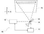
図1に、光走査システムの一例の概略図を示す。図1に示すように、光走査システム10は、駆動装置11の制御に従って光源装置12から照射された光を光偏向器13の有する反射面14により偏向して被走査面15を光走査するシステムである。
光走査システム10は、駆動装置11,光源装置12、反射面14を有する光偏向器13により構成される。
Hereinafter, embodiments of the present invention will be described in detail.
[Optical scanning system]
First, with reference to FIGS. 1 to 4, an optical scanning system to which the driving device according to the embodiment of the present invention is applied will be described in detail.
FIG. 1 shows a schematic view of an example of an optical scanning system. As shown in FIG. 1, the
The
駆動装置11は、例えばCPU(Central Processing Unit)およびFPGA(Field-Programmable Gate Array)等を備えた電子回路ユニットである。光偏向器13は、例えば反射面14を有し、反射面14を可動可能なMEMS(Micro Electromechanical Systems)デバイスである。光源装置12は、例えばレーザを照射するレーザ装置である。なお、被走査面15は、例えばスクリーンである。
駆動装置11は、取得した光走査情報に基づいて光源装置12および光偏向器13の制御命令を生成し、制御命令に基づいて光源装置12および光偏向器13に駆動信号を出力する。
The
The
光源装置12は、入力された駆動信号に基づいて光源の照射を行う。光偏向器13は、入力された駆動信号に基づいて反射面14を1軸方向または2軸方向の少なくともいずれかに可動させる。
これにより、例えば、光走査情報の一例である画像情報に基づいた駆動装置11の制御によって、光偏向器13の反射面14を所定の範囲で2軸方向に往復可動させ、反射面14に入射する光源装置12からの照射光を偏向して光走査することにより、被走査面15に任意の画像を投影することができる。
なお、光偏向器の詳細および本実施形態の駆動装置による制御の詳細については後述する。
次に、図2を参照して、光走査システム10の一例のハードウェア構成について説明する。
図2は、光走査システム10の一例のハードウェア構成図である。
図2に示すように、光走査システム10は、駆動装置11、光源装置12および光偏向器13を備え、それぞれが電気的に接続されている。
The
As a result, for example, by controlling the
The details of the optical deflector and the details of the control by the drive device of this embodiment will be described later.
Next, a hardware configuration of an example of the
FIG. 2 is a hardware configuration diagram of an example of the
As shown in FIG. 2, the
[駆動装置]
このうち、駆動装置11は、CPU20、RAM21(Random Access Memory)、ROM22(Read Only Memory)、FPGA23、外部I/F24、光源装置ドライバ25、光偏向器ドライバ26を備えている。
[Drive]
Of these, the
CPU20は、ROM22等の記憶装置からプログラムやデータをRAM21上に読み出し、処理を実行して、駆動装置11の全体の制御や機能を実現する演算装置である。
RAM21は、プログラムやデータを一時保持する揮発性の記憶装置である。
ROM22は、電源を切ってもプログラムやデータを保持することができる不揮発性の記憶装置であり、CPU20が光走査システム10の各機能を制御するために実行する処理用プログラムやデータを記憶している。
FPGA23は、CPU20の処理に従って、光源装置ドライバ25および光偏向器ドライバ26に適した制御信号を出力する回路である。
外部I/F24は、例えば外部装置やネットワーク等とのインタフェースである。外部装置には、例えば、PC(Personal Computer)等の上位装置、USBメモリ、SDカード、CD、DVD、HDD、SSD等の記憶装置が含まれる。また、ネットワークは、例えば自動車のCAN(Controller Area Network)やLAN(Local Area Network)、インターネット等である。外部I/F24は、外部装置との接続または通信を可能にする構成であればよく、外部装置ごとに外部I/F24が用意されてもよい。
The
The
The
The
The external I /
光源装置トライバは、入力された制御信号に従って光源装置12に駆動電圧等の駆動信号を出力する電気回路である。
光偏向器ドライバ26は、入力された制御信号に従って光偏向器13に駆動電圧等の駆動信号を出力する電気回路である。
駆動装置11において、CPU20は、外部I/F24を介して外部装置やネットワークから光走査情報を取得する。なお、CPU20が光走査情報を取得することができる構成であればよく、駆動装置11内のROM22やFPGA23に光走査情報を格納する構成としてもよいし、駆動装置11内に新たにSSD等の記憶装置を設けて、その記憶装置に光走査情報を格納する構成としてもよい。
ここで、光走査情報とは、被走査面15にどのように光走査させるかを示した情報であり、例えば、光走査により画像を表示する場合は、光走査情報は画像データである。また、例えば、光走査により光書込みを行う場合は、光走査情報は書込み順や書込み箇所を示した書込みデータである。他にも、例えば、光走査により物体認識を行う場合は、光走査情報は物体認識用の光を照射するタイミングと照射範囲を示す照射データである。
本実施形態に係る駆動装置11は、CPU20の命令および図2に示したハードウェア構成によって、次に説明する機能構成を実現することができる。
The light source device triber is an electric circuit that outputs a drive signal such as a drive voltage to the
The
In the
Here, the optical scanning information is information indicating how the surface to be scanned 15 is optical-scanned. For example, when displaying an image by optical scanning, the optical scanning information is image data. Further, for example, when optical writing is performed by optical scanning, the optical scanning information is write data indicating the writing order and the writing location. In addition, for example, when object recognition is performed by optical scanning, the optical scanning information is irradiation data indicating the timing and irradiation range of irradiating the light for object recognition.
The
[駆動装置の機能構成]
次に、図3を参照して、光走査システム10の駆動装置11の機能構成について説明する。図3は、光走査システムの駆動装置の一例の機能ブロック図である。
図3に示すように、駆動装置11は、機能として制御部30と駆動信号出力部31とを有する。
制御部30は、例えばCPU20、FPGA23等により実現され、外部装置から光走査情報を取得し、光走査情報を制御信号に変換して駆動信号出力部31に出力する。例えば、制御部30は、制御手段を構成し、外部装置等から画像データを光走査情報として取得し、所定の処理により画像データから制御信号を生成して駆動信号出力部31に出力する。
駆動信号出力部31は、印加手段を構成し、光源装置ドライバ25、光偏向器ドライバ26等により実現され、入力された制御信号に基づいて光源装置12または光偏向器13に駆動信号を出力する。駆動信号出力部31(印加手段)は、例えば、駆動信号を出力する対象ごとに設けられてもよい。
駆動信号は、光源装置12または光偏向器13の駆動を制御するための信号である。例えば、光源装置12においては、光源の照射タイミングおよび照射強度を制御する駆動電圧である。また、例えば、光偏向器13においては、光偏向器13の有する反射面14を可動させるタイミングおよび可動範囲を制御する駆動電圧である。なお、駆動装置は、光源装置12や受光装置等の外部装置から光源の照射タイミングや受光タイミングを取得し、これらを光偏向器13の駆動に同期するようにしてもよい。
[Functional configuration of drive unit]
Next, the functional configuration of the
As shown in FIG. 3, the
The
The drive signal output unit 31 constitutes an application means, is realized by the light
The drive signal is a signal for controlling the drive of the
[光走査処理]
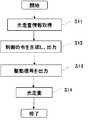
次に、図4を参照して、光走査システム10が被走査面15を光走査する処理について説明する。図4は、光走査システムに係る処理の一例のフローチャートである。
ステップS11において、制御部30は、外部装置等から光走査情報を取得する。
ステップS12において、制御部30は、取得した光走査情報から制御信号を生成し、制御信号を駆動信号出力部31に出力する。
ステップS13において、駆動信号出力部31は、入力された制御信号に基づいて駆動信号を光源装置12および光偏向器13に出力する。
ステップS14において、光源装置12は、入力された駆動信号に基づいて光照射を行う。また、光偏向器13は、入力された駆動信号に基づいて反射面14の可動を行う。光源装置12および光偏向器13の駆動により、任意の方向に光が偏向され、光走査される。
なお、上記光走査システム10では、1つの駆動装置11が光源装置12および光偏向器13を制御する装置および機能を有しているが、光源装置用の駆動装置および光偏向器用の駆動装置と、別体に設けてもよい。
また、上記光走査システム10では、一つの駆動装置11に光源装置12および光偏向器13の制御部30の機能および駆動信号出力部31の機能を設けているが、これらの機能は別体として存在していてもよく、例えば制御部30を有した駆動装置11とは別に駆動信号出力部31を有した駆動信号出力装置を設ける構成としてもよい。なお、上記光走査システム10のうち、反射面14を有した光偏向器13と駆動装置11により、光偏向を行う光偏向システムを構成してもよい。
[Optical scanning process]
Next, with reference to FIG. 4, a process in which the
In step S11, the
In step S12, the
In step S13, the drive signal output unit 31 outputs a drive signal to the
In step S14, the
In the
Further, in the
[画像投影装置]
次に、図5及び図6を参照して、本実施形態の駆動装置を適用した画像投影装置について詳細に説明する。
図5は、画像投影装置の一例であるヘッドアップディスプレイ装置500を搭載した自動車400の実施形態に係る概略図である。また、図6はヘッドアップディスプレイ装置500の一例の概略図である。
画像投影装置は、光走査により画像を投影する装置であり、例えばヘッドアップディスプレイ装置である。
図5に示すように、ヘッドアップディスプレイ装置500は、例えば、自動車400のウインドシールド(フロントガラス401等)の付近に設置される。ヘッドアップディスプレイ装置500から発せられる投射光Lがフロントガラス401で反射され、ユーザーである観察者(運転者402)に向かう。
これにより、運転者402は、ヘッドアップディスプレイ装置500によって投影された画像等を虚像として視認することができる。なお、ウインドシールドの内壁面にコンバイナを設置し、コンバイナによって反射する投射光によってユーザーに虚像を視認させる構成にしてもよい。
[Image projection device]
Next, with reference to FIGS. 5 and 6, an image projection device to which the driving device of the present embodiment is applied will be described in detail.
FIG. 5 is a schematic view of an embodiment of an
The image projection device is a device that projects an image by optical scanning, for example, a head-up display device.
As shown in FIG. 5, the head-up
As a result, the
図6に示すように、ヘッドアップディスプレイ装置500は、赤色、緑色、青色のレーザ光源501R,501G,501Bからレーザ光が出射される。出射されたレーザ光は、各レーザ光源に対して設けられるコリメータレンズ502,503,504と、2つのダイクロイックミラー505,506と、光量調整部507と、から構成される入射光学系を経た後、反射面14を有する光偏向器13にて偏向される。
そして、偏向されたレーザ光は、自由曲面ミラー509と、中間スクリーン510と、投射ミラー511とから構成される投射光学系を経て、スクリーンに投影される。
なお、上記ヘッドアップディスプレイ装置500では、レーザ光源501R,501G,501B、コリメータレンズ502,503,504、ダイクロイックミラー505,506は、光源ユニット530として光学ハウジングによってユニット化されている。
上記ヘッドアップディスプレイ装置500は、中間スクリーン510に表示される中間像を自動車400のフロントガラス401に投射することで、その中間像を運転者402に虚像として視認させる。
レーザ光源501R,501G,501Bから発せられる各色レーザ光は、それぞれ、コリメータレンズ502,503,504で略平行光とされ、2つのダイクロイックミラー505,506により合成される。合成されたレーザ光は、光量調整部507で光量が調整された後、反射面14を有する光偏向器13によって二次元走査される。光偏向器13で二次元走査された投射光Lは、自由曲面ミラー509で反射されて歪みを補正された後、中間スクリーン510に集光され、中間像を表示する。中間スクリーン510は、マイクロレンズが二次元配置されたマイクロレンズアレイで構成されており、中間スクリーン510に入射してくる投射光Lをマイクロレンズ単位で拡大する。
光偏向器13は、反射面14を2軸方向に往復可動させ、反射面14に入射する投射光Lを二次元走査する。この光偏向器13の駆動制御は、レーザ光源501R,501G,501Bの発光タイミングに同期して行われる。
以上、画像投影装置の一例としてのヘッドアップディスプレイ装置500の説明をしたが、画像投影装置は、反射面14を有した光偏向器13により光走査を行うことで画像を投影する装置であればよい。
例えば、机等に置かれ、表示スクリーン上に画像を投影するプロジェクタや、観測者の頭部等に装着される装着部材に搭載され、装着部材が有する反射透過スクリーンに投影、または眼球をスクリーンとして画像を投影するヘッドマウントディスプレイ装置等にも、同様に適用することができる。
また、画像投影装置は、車両や装着部材だけでなく、例えば、航空機、船舶、移動式ロボット等の移動体、あるいは、その場から移動せずにマニピュレータ等の駆動対象を操作する作業ロボットなどの非移動体に搭載されてもよい。
As shown in FIG. 6, the head-up
Then, the deflected laser beam is projected onto the screen via a projection optical system including a free
In the head-up
The head-up
The laser light of each color emitted from the
The
The head-up
For example, it is mounted on a projector that is placed on a desk or the like and projects an image on a display screen, or is mounted on a mounting member mounted on an observer's head or the like, and is projected onto a reflection / transmission screen of the mounting member, or an eyeball is used as a screen. The same can be applied to a head-mounted display device or the like that projects an image.
Further, the image projection device is not only a vehicle or a mounting member, but also a moving body such as an aircraft, a ship, or a mobile robot, or a work robot that operates a drive target such as a manipulator without moving from the place. It may be mounted on a non-moving body.
[光書込装置]
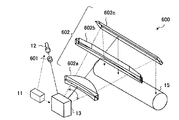
次に、図7及び図8を参照して、本実施形態の駆動装置11を適用した光書込装置について詳細に説明する。
図7は、光書込装置600を組み込んだ画像形成装置の一例である。また、図8は、光書込装置の一例の概略図である。
図7に示すように、上記光書込装置600は、レーザ光によるプリンタ機能を有するレーザプリンタ650等に代表される画像形成装置の構成部材として使用される。画像形成装置において光書込装置600は、1本または複数本のレーザビームで被走査面15である感光体ドラムを光走査することにより、感光体ドラムに光書込を行う。
図8に示すように、光書込装置600において、レーザ素子などの光源装置12からのレーザ光は、コリメータレンズなどの結像光学系601を経た後、反射面14を有する光偏向器13により1軸方向または2軸方向に偏向される。
そして、光偏向器13で偏向されたレーザ光は、その後、第一レンズ602aと第二レンズ602b、反射ミラー部602cからなる走査光学系602を経て、被走査面15(例えば感光体ドラムや感光紙)に照射し、光書込みを行う。走査光学系602は、被走査面15にスポット状に光ビームを結像する。
また、光源装置12および反射面14を有する光偏向器13は、駆動装置11の制御に基づき駆動する。
このように上記光書込装置600は、レーザ光によるプリンタ機能を有する画像形成装置の構成部材として使用することができる。
また、走査光学系を異ならせて1軸方向だけでなく2軸方向に光走査可能にすることで、レーザ光をサーマルメディアに偏向して光走査し、加熱することで印字するレーザラベル装置等の画像形成装置の構成部材として使用することができる。
上記光書込装置に適用される反射面14を有した光偏向器13は、ポリゴンミラー等を用いた回転多面鏡に比べ駆動のための消費電力が小さいため、光書込装置の省電力化に有利である。
また、光偏向器13の振動時における風切り音は回転多面鏡に比べ小さいため、光書込装置の静粛性の改善に有利である。光書込装置は回転多面鏡に比べ設置スペースが圧倒的に少なくて済み、また光偏向器13の発熱量もわずかであるため、小型化が容易であり、よって画像形成装置の小型化に有利である
[Optical writing device]
Next, with reference to FIGS. 7 and 8, the optical writing device to which the
FIG. 7 is an example of an image forming apparatus incorporating the
As shown in FIG. 7, the
As shown in FIG. 8, in the
Then, the laser beam deflected by the
Further, the
As described above, the
Further, by making the scanning optical system different so that light scanning can be performed not only in the uniaxial direction but also in the biaxial direction, the laser beam is deflected to the thermal media to scan the light, and the laser label device for printing by heating and the like. It can be used as a constituent member of the image forming apparatus of.
The
Further, since the wind noise when the
[物体認識装置]
次に、図9及び図10を参照して、上記本実施形態の駆動装置を適用した物体認識装置について詳細に説明する。
図9は、物体認識装置の一例であるレーザレーダ装置を搭載した自動車の概略図である。また、図10はレーザレーダ装置の一例の概略図である。
物体認識装置は、対象方向の物体を認識する装置であり、例えばレーザレーダ装置である。
図9に示すように、レーザレーダ装置700は、例えば自動車701に搭載され、対象方向を光走査して、対象方向に存在する被対象物702からの反射光を受光することで、被対象物702を認識する。
図10に示すように、光源装置12から出射されたレーザ光は、発散光を略平行光とする光学系であるコリメートレンズ703と、平面ミラー704とから構成される入射光学系を経て、反射面14を有する光偏向器13で1軸もしくは2軸方向に走査される。
そして、投光光学系である投光レンズ705等を経て装置前方の被対象物702に照射される。光源装置12および光偏向器13は、駆動装置11により駆動を制御される。被対象物702で反射された反射光は、光検出器709により光検出される。
すなわち、反射光は受光光学系である集光レンズ706等を経て撮像素子707により受光され、撮像素子707は検出信号を信号処理回路708に出力する。信号処理回路708は、入力された検出信号に2値化やノイズ処理等の所定の処理を行い、結果を測距回路710に出力する。
測距回路710は、光源装置12がレーザ光を発光したタイミングと、光検出器709でレーザ光を受光したタイミングとの時間差、または受光した撮像素子707の画素ごとの位相差によって、被対象物702の有無を認識し、さらに被対象物702との距離情報を算出する。
反射面14を有する光偏向器13は多面鏡に比べて破損しづらく、小型であるため、耐久性の高い小型のレーダ装置を提供することができる。
このようなレーダレーダ装置は、例えば車両、航空機、船舶、ロボット等に取り付けられ、所定範囲を光走査して障害物の有無や障害物までの距離を認識することができる。
上記物体認識装置では、一例としてのレーザレーダ装置700の説明をしたが、物体認識装置は、反射面14を有した光偏向器13を駆動装置11で制御することにより光走査を行い、光検出器により反射光を受光することで被対象物702を認識する装置であればよく、上述した実施形態に限定されるものではない。
例えば、手や顔を光走査して得た距離情報から形状等の物体情報を算出し、記録と参照することで対象物を認識する生体認証や、対象範囲への光走査により侵入物を認識するセキュリティセンサ、光走査により得た距離情報から形状等の物体情報を算出して認識し、3次元データとして出力する3次元スキャナの構成部材などにも同様に適用することができる。
[Object recognition device]
Next, with reference to FIGS. 9 and 10, an object recognition device to which the driving device of the present embodiment is applied will be described in detail.
FIG. 9 is a schematic view of an automobile equipped with a laser radar device, which is an example of an object recognition device. Further, FIG. 10 is a schematic view of an example of a laser radar device.
The object recognition device is a device that recognizes an object in the target direction, for example, a laser radar device.
As shown in FIG. 9, the
As shown in FIG. 10, the laser light emitted from the
Then, the
That is, the reflected light is received by the
The
Since the
Such a radar A radar device can be attached to, for example, a vehicle, an aircraft, a ship, a robot, or the like, and can lightly scan a predetermined range to recognize the presence or absence of an obstacle and the distance to the obstacle.
In the above-mentioned object recognition device, the
For example, biometric authentication that recognizes an object by calculating object information such as shape from distance information obtained by light scanning the hand or face and referring to it as a record, or recognizing an intruder by light scanning the target range. It can also be applied to a security sensor, a component of a three-dimensional scanner that calculates and recognizes object information such as a shape from distance information obtained by optical scanning, and outputs it as three-dimensional data.
[パッケージング]
次に、図11を参照して、本実施形態の駆動装置により制御される光偏向器のパッケージングについて説明する。
図11は、パッケージングされた光偏向器の一例の概略図である。
図11に示すように、光偏向器13は、パッケージ部材801の内側に配置される取付部材802に取り付けられ、パッケージ部材の一部を透過部材803で覆われて、密閉されることでパッケージングされる。
さらに、パッケージ内は窒素等の不活性ガスが密封されている。これにより、光偏向器13の酸化による劣化が抑制され、さらに温度等の環境の変化に対する耐久性が向上する。
次に、以上に説明した光偏向システム、光走査システム、画像投射装置、光書込装置、物体認識装置に使用される光偏向器の詳細および本実施形態の駆動装置による制御の詳細について説明する。
[Packaging]
Next, with reference to FIG. 11, the packaging of the optical deflector controlled by the driving device of the present embodiment will be described.
FIG. 11 is a schematic diagram of an example of a packaged light deflector.
As shown in FIG. 11, the
Further, the package is sealed with an inert gas such as nitrogen. As a result, deterioration of the
Next, the details of the optical deflector used in the optical deflection system, the optical scanning system, the image projection device, the optical writing device, and the object recognition device described above and the details of the control by the driving device of the present embodiment will be described. ..
[光偏向器の詳細]
まず、図12〜図14を参照して、光偏向器について詳細に説明する。
図12は、2軸方向に光偏向可能な別タイプの光偏向器の平面図である。図13は、図12のP−P’断面図である。図14は図12のQ−Q’断面図である。図12に示すように、光偏向器13は、入射した光束Lを反射するミラー部101と、ミラー部101に接続され、ミラー部101をY軸に平行な第1軸O1周りに駆動する第1駆動部110a、110bと、を有している。
光偏向器13はまた、ミラー部101および第1駆動部110a、110bを支持する第1支持部120を有している。
光偏向器13はまた、第1支持部120に接続され、ミラー部101および第1支持部120をX軸に平行な第2軸O2周りに駆動する第2駆動部130a、130bと、第2駆動部130a、130bを支持する枠体部たる第2支持部140と、を有している。
なお、本実施形態における第1駆動部110a、110bと、ミラー部101と、第1支持部120とは、第2軸O2を中心に回転する可動部を構成している。また、第2駆動部130a、130bは、かかる可動部を第2支持部140に対して支持する。
光偏向器13は、第1駆動部110a、110bおよび第2駆動部130a、130bおよび駆動装置に電気的に接続される電極接続部150と、電極接続部150から第1駆動部110a、110bまで延びた通電路たる電極配線151と、を有している。
[Details of optical deflector]
First, the optical deflector will be described in detail with reference to FIGS. 12 to 14.
FIG. 12 is a plan view of another type of light deflector capable of light deflecting in the biaxial direction. FIG. 13 is a cross-sectional view taken along the line PP'of FIG. FIG. 14 is a cross-sectional view taken along the line QQ'of FIG. As shown in FIG. 12, the
The
The
The
The
光偏向器13は、例えば、1枚のSOI(Silicon On Insulator)基板をエッチング処理等により成形し、成形した基板上に反射面14や第1圧電駆動部112a、112b、第2圧電駆動部131a〜131f、132a〜132f、電極接続部150等を形成することで、各構成部が一体的に形成されている。
なお、上記の各構成部の形成は、SOI基板の成形後に行ってもよいし、SOI基板の成形中に行ってもよい。
The
The formation of each of the above-mentioned constituent parts may be performed after molding the SOI substrate, or may be performed during molding of the SOI substrate.
SOI基板は、図13、図14に示すように、例えば単結晶シリコン(Si)からなる第1のシリコン層たるシリコン支持層161と、シリコン支持層161の上部に形成された酸化シリコン層162と、酸化シリコン層162の上に形成された第2のシリコン層たるシリコン活性層163と、を有するシリコン基板である。
As shown in FIGS. 13 and 14, the SOI substrate includes, for example, a
シリコン活性層163は、X軸方向またはY軸方向に対してZ軸方向への厚みが小さいため、シリコン活性層163のみで構成された部材は、弾性を有する弾性部としての機能を備える。
Since the silicon
なお、SOI基板は、必ず平面状である必要はなく、曲率等を有していてもよい。また、エッチング処理等により一体的に成形でき、部分的に弾性を持たせることができる基板であれば光偏向器13の形成に用いられる部材はSOI基板に限られない。
The SOI substrate does not necessarily have to be flat, and may have a curvature or the like. Further, the member used for forming the
ミラー部101は、例えば、円形状のミラー部基体102と、ミラー部基体の+Z側の面上に形成された反射面14とから構成される。ミラー部基体102は、例えば、シリコン活性層163から構成される。
反射面14は、例えば、アルミニウム、金、銀等を含む金属薄膜で構成される。また、ミラー部101は、ミラー部基体102の−Z側の面にミラー部補強用のリブが形成されていてもよい。
リブは、例えば、シリコン支持層161および酸化シリコン層162から構成され、可動によって生じる反射面14の歪みを抑制することができる。
The
The
The rib is composed of, for example, a
第1駆動部110a、110bは、ミラー部基体102に一端が接続し、第1軸方向にそれぞれ延びてミラー部101を可動可能に支持する2つのトーションバー111a、111bと、一端がトーションバーに接続され、他端が第1支持部の内周部に接続される第1圧電駆動部112a、112bと、から構成される。
The
図13に示すように、トーションバー111a、111bはシリコン活性層163から構成される。また、第1圧電駆動部112a、112bは、弾性部であるシリコン活性層163の+Z側の面上に下部電極201と、圧電部202と、上部電極203とが順に積層して形成される。
上部電極203および下部電極201は、例えば金(Au)または白金(Pt)等を用いて構成される。
圧電部202は、例えば、圧電材料であるPZT(チタン酸ジルコン酸鉛)を用いた圧電膜で構成される。
以降の説明では、特に必要のある場合には下部電極201と、圧電部202と、上部電極203とをまとまりとして圧電駆動部との文言を用いる。
As shown in FIG. 13, the
The
The
In the following description, when it is particularly necessary, the wording of the
第1支持部120は、例えば、シリコン支持層161、酸化シリコン層162、シリコン活性層163から構成され、ミラー部101を囲うように形成された矩形形状の支持体である。
The
第2駆動部130a、130bは、例えば、折り返すように連結された複数の第2圧電駆動部131a〜131f、132a〜132fから構成されており、第2駆動部130a、130bの一端は第1支持部120の外周部に接続され、他端は第2支持部140の内周部に接続されている。
このとき、第2駆動部130aと第1支持部120の接続箇所および第2駆動部130bと第1支持部120の接続箇所、さらに第2駆動部130aと第2支持部140の接続箇所および第2駆動部130bと第2支持部140の接続箇所は、反射面14の中心に対して点対称となっている。
The
At this time, the connection points between the
図14に示すように、第2駆動部130a、130bは、弾性部であるシリコン活性層163の+Z側の面上に下部電極201、圧電部202、上部電極203の順に形成されて構成される。上部電極203および下部電極201は、例えば金(Au)または白金(Pt)等を用いて構成される。圧電部202は、例えば、圧電材料であるPZT(チタン酸ジルコン酸鉛)を用いた圧電体である。
As shown in FIG. 14, the
第2支持部140は、例えば、シリコン支持層161、酸化シリコン層162、シリコン活性層163から構成され、ミラー部101、第1駆動部110a、110b、第1支持部120および第2駆動部130a、130bを囲うように形成された矩形の支持体である。
The
電極接続部150は、例えば、第2支持部140の+Z側の面上に形成され、第1圧電駆動部112a、112b、第2圧電駆動部131a〜131fの各上部電極203および各下部電極201,および駆動装置11にアルミニウム(Al)等を用いて構成された電極配線151を介して電気的に接続されている。
なお、上部電極203または下部電極201は、それぞれが電極接続部150と直接接続されていてもよいし、電極同士を接続して間接的に接続されていてもよい。
The
The
また本実施形態では、圧電部202が弾性部であるシリコン活性層163の一面(+Z側の面)のみに形成された場合を一例として説明したが、弾性部の他の面(例えば−Z側の面)に設けても良いし、弾性部の一面および他面の双方に設けても良い。
Further, in the present embodiment, the case where the
また、ミラー部101を第1軸周りまたは第2軸周りに駆動可能であれば、各構成部の形状は実施形態の形状に限定されない。例えば、トーションバー111a、111bや第1圧電駆動部112a、112bが曲率を有した形状を有していてもよい。
Further, the shape of each component is not limited to the shape of the embodiment as long as the
図14に示すように、第1圧電駆動部112a、112bと、第2圧電駆動部131a〜131f、132a〜132fとはいずれも、当該第2圧電駆動部の表面の少なくとも一部を覆うように、絶縁膜たる絶縁層153を有している。
絶縁層153は、上部電極203と、下部電極201との間の絶縁を保つように形成された保護膜たる層関絶縁層であり、例えばSiO2等を用いて構成される。
絶縁層153には、図15に示して後述するように電極配線151を接続するための開口部154が形成されている。
As shown in FIG. 14, the first
The insulating
The insulating
本実施形態では、電極配線151は、図15に示すように、隣り合う2つの第2圧電駆動部131aと第2圧電駆動部131bとを接続する接続部としての機能を有している。
なお以降の説明では例として特に第2圧電駆動部131aと第2圧電駆動部131bとを接続する場合について述べるが、第2圧電駆動部131a〜131f及び第2圧電駆動部132a〜132fについて同様の構成を有している。
In the present embodiment, as shown in FIG. 15, the
In the following description, the case where the second
電極配線151は、絶縁層153に形成された開口部154を介して上部電極203に電圧を印加する接続部であり、最も−Z側の層に後述するパッシベーション膜としての機能を有するバリア層を備えている。本実施形態では、電極配線151は、バリア層となるSiO2の上層にAlやAl合金などの導電層が積層された積層構造である。本実施形態のように、上部電極203の側面203bと当接することとすれば、このように電極配線151の最下層を絶縁性のバリア層としても良いため、基板全体の保護性が向上する。
開口部154は、絶縁層153にエッチングなどの手法を用いて開けられた開口である。なお、かかる開口部154を設けるために、下部電極201は、圧電部202よりも大きく、圧電部202は上部電極203よりも大きくなるように、それぞれの幅と長さとが調整されることが望ましい。
開口部154は、+Z方向側から見たときに上部電極203と、圧電部202とが重なった部分と、重なっていない部分と、を含む位置に形成されている。言い換えると開口部154は、上部電極203の+Z方向側の一部と、圧電部202の+Z方向側の一部とを覆うように、上部電極203のX方向の端部に形成されている。
The
The
The
電極配線151は、端部が上部電極203と圧電部202とに当接して、隣り合う2つの第2圧電駆動部131a、131bの上部電極203と圧電部202とを接続している。さらにいうと、図16に示すように、電極配線151は、上部電極203の上面203aと、側面203bとに当接するとともに、圧電部202の上面202aにも当接するように配置されている。
The end of the
[駆動装置の制御の詳細]
次に、光偏向器の第1駆動部110a、110bおよび第2駆動部130a、130bを駆動させる駆動装置11の制御の詳細について説明する。
[Details of drive unit control]
Next, the details of the control of the
第1駆動部110a、110b、第2駆動部130a、130bが有する第2圧電駆動部131a〜131fは、分極方向に正または負の電圧が印加されると印加電圧の電位に比例した変形(例えば、伸縮)が生じ、いわゆる逆圧電効果を発揮する。第1駆動部110a,110b,第2駆動部130a、130bは、上記の逆圧電効果を利用してミラー部101を可動させる。
The second
このとき、ミラー部101の反射面14に入射した光束が偏向される角度を振れ角とよぶ。圧電部に電圧を印加していないときの振れ角をゼロとし、その角度よりも偏向角度が大きい場合を正の振れ角、小さい場合を負の振れ角とする。
At this time, the angle at which the light flux incident on the reflecting
まず、第1駆動部を駆動させる駆動装置の制御について説明する。
第1駆動部110a、110bでは、第1圧電駆動部112a、112bが有する圧電部202に、上部電極203および下部電極201を介して駆動電圧が並列に印加されると、それぞれの圧電部202が変形する。この圧電部202の変形による作用により、第1圧電駆動部112a、112bが屈曲変形する。
その結果、2つのトーションバー111a、111bのねじれを介してミラー部101に第1軸O1周りの駆動力が作用し、ミラー部101が第1軸O1周りに可動する。第1駆動部110a、110bに印加される駆動電圧は、駆動装置11によって制御される。
First, the control of the drive device for driving the first drive unit will be described.
In the
As a result, the two
そこで、駆動装置11によって、第1駆動部110a、110bが有する第1圧電駆動部112a、112bに所定の正弦波形の駆動電圧を並行して印加することで、ミラー部101を、第1軸周りに所定の正弦波形の駆動電圧の周期で可動させることができる。
Therefore, the
特に、例えば、正弦波形電圧の周波数がトーションバー111a、111bの共振周波数と同程度である約20kHzに設定された場合、トーションバー111a、111bのねじれによる機械的共振が生じるのを利用して、ミラー部101を約20kHzで共振振動させることができる。
In particular, for example, when the frequency of the sinusoidal waveform voltage is set to about 20 kHz, which is about the same as the resonance frequency of the
次に、図17〜図21を参照して、第2駆動部を駆動させる駆動装置の制御について説明する。 Next, control of the driving device for driving the second driving unit will be described with reference to FIGS. 17 to 21.
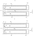
図17は、光偏向器の第2駆動部130bの駆動を模式的に表した模式図である。斜線で表されている領域がミラー部101等である。
FIG. 17 is a schematic view schematically showing the driving of the
第2駆動部130aが有する複数の第2圧電駆動部131a〜131fのうち、最もミラー部に距離が近い第2圧電駆動部(131a)から数えて偶数番目の第2圧電駆動部、すなわち第2圧電駆動部131b、131d、131fを圧電駆動部群Aとする。
また、さらに第2駆動部130bが有する複数の第2圧電駆動部132a〜132fのうち、最もミラー部に距離が近い第2圧電駆動部(132a)から数えて奇数番目の第2圧電駆動部、すなわち第2圧電駆動部132a、132c、132eを同様に圧電駆動部群Aとする。圧電駆動部群Aは、駆動電圧が並行に印加されると、図15(a)に示すように、圧電駆動部群Aが同一方向に屈曲変形し、正の振れ角となるようにミラー部101が第2軸O2周りに可動する。
Of the plurality of second
Further, among the plurality of second
また、第2駆動部130aが有する複数の第2圧電駆動部131a〜131fのうち、最もミラー部に距離が近い第2圧電駆動部(131a)から数えて奇数番目の第2圧電駆動部、すなわち第2圧電駆動部131a、131c、131eを圧電駆動部群Bとする。
また、さらに第2駆動部130bが有する複数の第2圧電駆動部132a〜132fのうち、最もミラー部に距離が近い第2圧電駆動部(132a)から数えて偶数番目の第2圧電駆動部、すなわち、132b、132d、132fを同様に圧電駆動部群Bとする。圧電駆動部群Bは、駆動電圧が並行に印加されると、図15(b)に示すように、圧電駆動部群Bが同一方向に屈曲変形し、負の振れ角となるようにミラー部101が第2軸O2周りに可動する。
Further, among the plurality of second
Further, among the plurality of second
図17(a)、(b)に示すように、第2駆動部130aまたは130bでは、圧電駆動部群Aが有する複数の圧電部202または圧電駆動部群Bが有する複数の圧電部202を屈曲変形させることにより、屈曲変形による可動量を累積させ、ミラー部101の第2軸周りの振れ角を大きくすることができる。
As shown in FIGS. 17A and 17B, in the
例えば、図12に示すように、第2駆動部130a、130bが、第1支持部の中心点に対して第1支持部に点対称で接続されている。そのため、圧電駆動部群Aに駆動電圧を印加すると、第2駆動部130aでは第1支持部と第2駆動部130aの接続部に+Z方向に動かす駆動力が生じ、第2駆動部130bでは第1支持部と第2駆動部130bの接続部に−Z方向に動かす駆動力が生じ、可動量が累積されてミラー部101の第2軸O2周りの振れ角度を大きくすることができる。
For example, as shown in FIG. 12, the
また、電圧が印加されていない、または、電圧印加による圧電駆動部群Aによるミラー部101の可動量と電圧印加による圧電駆動群Bによるミラー部101の可動量が釣り合っている時は、振れ角はゼロとなる。
Further, when no voltage is applied, or when the movable amount of the
図17(a)〜図17(b)を連続的に繰り返すように第2圧電駆動部131a〜131fに駆動電圧を印加することにより、ミラー部101を第2軸O2周りに駆動させることができる。
By applying a drive voltage to the second
[駆動電圧]
第2駆動部130a、130bに印加される駆動電圧は、駆動装置11によって制御される。
図16を参照して、圧電駆動部群Aに印加される駆動電圧(以下、駆動電圧A)、圧電駆動部群Bに印加される駆動電圧(以下、駆動電圧B)について説明する。また、駆動電圧A(第1駆動電圧)を印加する印加手段を第1印加手段、駆動電圧B(第2駆動電圧)を印加する印加手段を第2印加手段とする。
[Drive voltage]
The drive voltage applied to the
With reference to FIG. 16, the drive voltage applied to the piezoelectric drive unit group A (hereinafter, drive voltage A) and the drive voltage applied to the piezoelectric drive unit group B (hereinafter, drive voltage B) will be described. Further, the application means for applying the drive voltage A (first drive voltage) is referred to as the first application means, and the application means for applying the drive voltage B (second drive voltage) is referred to as the second application means.
図18(a)は、光偏向器の圧電駆動部群Aに印加される駆動電圧Aの波形の一例である。図18(b)は、光偏向器の圧電駆動部群Bに印加される駆動電圧Bの波形の一例である。図18(c)は、駆動電圧Aの波形と駆動電圧Bの波形を重ね合わせた図である。 FIG. 18A is an example of the waveform of the drive voltage A applied to the piezoelectric drive unit group A of the optical deflector. FIG. 18B is an example of the waveform of the drive voltage B applied to the piezoelectric drive unit group B of the optical deflector. FIG. 18C is a diagram in which the waveform of the drive voltage A and the waveform of the drive voltage B are superimposed.
図18(a)に示すように、圧電駆動部群Aに印加される駆動電圧Aの波形は、例えば、ノコギリ波状の波形であり、周波数は、例えば60HZである。
また、駆動電圧Aの波形は、電圧値が極小値から次の極大値まで増加していく立ち上がり期間の時間幅をTrA、電圧値が極大値から次の極小値まで減少していく立ち下がり期間の時間幅をTfAとしたとき、例えば、TrA:TfA=9:1となる比率があらかじめ設定されている。このとき、一周期に対するTrAの比率を駆動電圧Aのシンメトリという。
As shown in FIG. 18A, the waveform of the drive voltage A applied to the piezoelectric drive unit group A is, for example, a sawtooth waveform, and the frequency is, for example, 60 Hz.
Further, in the waveform of the drive voltage A, the time width of the rising period in which the voltage value increases from the minimum value to the next maximum value is TrA, and the falling period in which the voltage value decreases from the maximum value to the next minimum value. When the time width of is TfA, for example, the ratio of TrA: TfA = 9: 1 is preset. At this time, the ratio of TrA to one cycle is called the symmetry of the drive voltage A.
図18(b)に示すように、圧電駆動部群Bに印加される駆動電圧Bの波形は、例えば、ノコギリ波状の波形であり、周波数は、例えば60HZである。
また、駆動電圧Bの波形は、電圧値が極小値から次の極大値まで増加していく立ち上がり期間の時間幅をTrB、電圧値が極大値から次の極小値まで減少していく立ち下がり期間の時間幅をTfBとしたとき、例えば、TfB:TrB=9:1となる比率があらかじめ設定されている。このとき、一周期に対するTfBの比率を駆動電圧Bのシンメトリという。
また、図18(c)に示すように、例えば、駆動電圧Aの波形の周期TAと駆動電圧Bの波形の周期TBは、同一となるように設定されている。
As shown in FIG. 18B, the waveform of the drive voltage B applied to the piezoelectric drive unit group B is, for example, a sawtooth waveform, and the frequency is, for example, 60 Hz.
Further, in the waveform of the drive voltage B, the time width of the rising period in which the voltage value increases from the minimum value to the next maximum value is TrB, and the falling period in which the voltage value decreases from the maximum value to the next minimum value. When the time width of is TfB, for example, the ratio of TfB: TrB = 9: 1 is preset. At this time, the ratio of TfB to one cycle is called the symmetry of the drive voltage B.
Further, as shown in FIG. 18C, for example, the period TA of the waveform of the drive voltage A and the period TB of the waveform of the drive voltage B are set to be the same.
なお、上記の駆動電圧Aおよび駆動電圧Bのノコギリ波状の波形は、例えば、正弦波の重ね合わせによって生成される。
また、本実施形態では、駆動電圧A、Bとしてノコギリ波状の波形の駆動電圧を用いているが、これに限らず、ノコギリ波状の波形の頂点を丸くした波形の駆動電圧や、ノコギリ波状の波形の直線領域を曲線とした波形の駆動電圧など、光偏向器のデバイス特性に応じて波形を変えることも可能である。この場合、シンメトリは、一周期に対する立ち上がり時間の比率、または一周期に対する立ち下がり時間の比率となる。このとき、立ち上がり時間、立ち下がり時間のどちらを基準にするかは、任意に設定してもよい。
The sawtooth waveforms of the drive voltage A and the drive voltage B are generated, for example, by superimposing sine waves.
Further, in the present embodiment, the drive voltage of the sawtooth waveform is used as the drive voltages A and B, but the present invention is not limited to this, and the drive voltage of the waveform with the apex of the sawtooth waveform rounded and the sawtooth waveform It is also possible to change the waveform according to the device characteristics of the optical deflector, such as the drive voltage of the waveform with the linear region of. In this case, the symmetry is the ratio of the rise time to one cycle or the ratio of the fall time to one cycle. At this time, which of the rise time and the fall time is used as a reference may be arbitrarily set.
次に、かかる駆動部の製造方法について説明する。
なお、以降の説明においても、圧電駆動部のうち特に第2圧電駆動部131aについて説明するが、かかる構成に限定されるものではなく、光偏向器13において圧電材料を用いた部分については同様の構成を有している。
図19(a)に示すように、基板材料としてシリコン支持層161と、酸化シリコン層162と、シリコン活性層163と、が積層されたSOI基板上に、下部電極材料1904と、圧電材料1905と、上部電極材料1906と、を層状に形成する。
次に図19(b)に示すように、ドライエッチングによって上部電極材料1906のパターニングと、圧電材料1905のパターニングと、下部電極材料1904のパターニングとを行い、圧電駆動部131aの圧電部材の形状を形成する。
さらに、図19(c)のように、全面に絶縁材料1908としてSiO2をCVD法により形成する。
絶縁材料1908が成膜されると、図19(d)に示すように、コンタクトホールとして絶縁材料1908に開口部154をドライエッチングによって形成する。このとき開口部154は、上部電極材料1906と圧電材料1905とがZ方向からみて重複して形成された部分と、圧電材料1905が形成されて上部電極材料1906が存在しない部分と、を含むように形成されている。
Next, a method of manufacturing such a drive unit will be described.
In the following description, the second
As shown in FIG. 19A, the
Next, as shown in FIG. 19B, the
Further, as shown in FIG. 19C, SiO 2 is formed on the entire surface as the insulating
When the insulating
絶縁材料1908上に配線部材1910を用いて配線パターンを形成する(図19(e))。このとき、開口部154の内部に配線部材1910が充填されることにより、配線部材1910が上部電極材料1906と圧電材料1905との両方に当接した態様で配線パターンが形成される。
配線部材1910によって配線パターンが形成された後、図19(f)に示すように基板全体にパッシベーション膜1911を形成する。パッシベーション膜としては例えばSiNをCVD法により成膜することで形成する。
かかるパッシベーション膜1911は、外界からのガス、水分などからパターニングされた基板を保護するための保護膜としての機能を有している。
A wiring pattern is formed on the insulating
After the wiring pattern is formed by the
The
シリコン活性層163に形成したい構造、具体的には図12に示したような構造に合わせて、図19(g)に示すようにドライエッチングによってパッシベーション膜1911、絶縁材料1908を加工する。さらに、図19(h)に示すように、第2圧電駆動部131aが形成される部分のシリコン支持層161を−Z方向側からエッチングによって除去して、圧電部材による梁状部分の反りなどが生じやすいように加工する。
このように、シリコン活性層163がエッチングにより除去されている領域においてシリコン支持層161の加工を行うと、シリコン支持層161が除去されて所謂抜き部分が形成される。同様に、シリコン活性層163が残された部分においてシリコン支持層161の加工を行うことで、シリコン活性層163が残って第2圧電駆動部131aが電圧印加によって伸縮するときの変形が容易に行える。
The
When the
かかる製造方法によれば、第2圧電駆動部131a〜131fへの繰り返しの電圧印加に対する開口部154の変形を抑制できるから、長時間動作した場合にも開口部154における剥離が生じにくく、信頼性・耐久性に優れた光偏向器が提供可能である。
According to such a manufacturing method, deformation of the
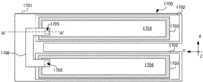
さて、従来の光偏向器では、図24、図25に示すように、第2圧電駆動部に相当する梁状部材1700は、シリコン活性層1701上に下部電極1702と、圧電膜1703と、上部電極1704とが積層して形成されている。
梁状部材1700は、上部電極1703を覆うように形成された絶縁膜1707と、絶縁膜1707の一部に開けられた開口たるコンタクトホール1705と、コンタクトホール1705を介して上部電極1704と当接する配線1706と、を有している。
By the way, in the conventional optical deflector, as shown in FIGS. 24 and 25, the beam-shaped
The beam-shaped
梁状部材1700においては、図25にR−R’断面図として示すように、コンタクトホール1705が上部電極1704上に設けられている。また、配線1706は上部電極1704とのみ当接する態様で保持されている。
In the beam-shaped
さて、梁状部材1700が上下動するときには上部電極1704と下部電極1702との間に挟まれた圧電膜1703が伸縮することによって上下動が生じている。すなわち、コンタクトホール1705が形成された部位においても梁状部材1700は圧電膜1703の伸縮変形に伴って上下方向へ振動する。
このような変形が繰り返し行われることによって、コンタクトホール1705の付近には、繰り返し応力が生じて、配線1706と上部電極1704との間の剥離やクラックなどの故障が生じるおそれがあった。特に、図24に示すように、従来の光偏向器においては、コンタクトホール1705を囲う周囲全てで圧電膜が伸縮するため、配線1706と上部電極1704との間の剥離やクラックが生じやすかった。
このような剥離やクラックを生じにくくさせるためには、コンタクトホール1705の周囲で圧電膜の伸縮を低減させる、または、上部電極1704と配線1706との間の密着力を向上させることが望ましい。こうした密着力は一般に、接触面積と、接触面の粗さによって大きく変動することが知られている。
When the beam-shaped
By repeatedly performing such deformation, repeated stress is generated in the vicinity of the
In order to prevent such peeling and cracking from occurring, it is desirable to reduce the expansion and contraction of the piezoelectric film around the
そこで、本実施形態では、反射面14を有するミラー部101と、複数の弾性部130a、130bが蛇行状に連続して形成され、ミラー部101を支持する支持部120と、弾性部130a、130bに個別に設けられた複数の第2圧電駆動部131a〜131fと、第2圧電駆動部131a〜131fを少なくとも部分的に覆う絶縁膜153と、絶縁膜153に設けられた開口部154を介して少なくとも2つの第2圧電駆動部131a、131bを接続する接続部と、を有している。
また第2圧電駆動部131a、131bは、下部電極201と、圧電部202と、上部電極203と、が積層されており、電極配線151は、第2圧電駆動部131aの上部電極203および圧電部202に当接する。
Therefore, in the present embodiment, the
Further, in the second
かかる構成について、更に詳しく説明する。図15、16に示すように、本実施形態では、電極配線151が圧電部202と上部電極203とに当接するように、開口部154が形成されている。したがって、電極配線151は、上部電極203の上面203aと、側面203bと、圧電部202の上面202aと、に当接する。
すでに述べたように、圧電部202の変形は、上部電極203と下部電極201との間に電圧が印加されて生じる。しかしながら、本実施形態では、開口部154が上部電極203の両端部に設けられている。さらに言うと、開口部154は、上部電極203の±X方向の端部に重複するように、形成されている。
このように、開口部154が上部電極203が形成されない部分にも形成されることとすれば、図19の拡大図において一点破線で示す部分には、上部電極203がないので圧電部202の変形が生じない。すなわちコンタクトホールたる開口部154の周囲で圧電膜の伸縮を低減することができる。
かかる構成により、上部電極203と電極配線151との間の剥離やクラックの進行を抑制して、故障の発生が低減される。
Such a configuration will be described in more detail. As shown in FIGS. 15 and 16, in the present embodiment, the
As described above, the deformation of the
As described above, if the
With such a configuration, peeling and progress of cracks between the
上記効果に加えてさらに、かかる構成により電極配線151と上部電極203との接触面積が向上するとともに、粗い上部電極203の側面と当接するから、密着力が向上して第2圧電駆動部131aの変形が繰り返し生じるときにも剥離、クラックの進行を抑制して故障の発生をより低減する。
また、電極配線151が上部電極203の側面203bと圧電部202の上面202aとに囲繞された態様で固定されるから、剥離方向に働く力が分散してより密着力が向上する。
In addition to the above effects, the contact area between the
Further, since the
また本実施形態では、電極配線151は、蛇行状に形成された第2圧電駆動部131a〜131fの折り返し部分に、隣り合う第2圧電駆動部131a、131bを接続するように配置されている。
かかる構成により、第2圧電駆動部131a、131bの変形が生じにくい折り返し部133に電極配線151が配置されるから、第2圧電駆動部131a、131bの変形による剥離やクラックの進行を抑制して、故障の発生が低減される。
Further, in the present embodiment, the
With this configuration, the
本実施形態の変形例として、開口部154の位置関係について述べる。
なお、以降の変形例においては、第1の実施形態と同様の構成については同一の付番をして説明は適宜省略する。
本変形例では、開口部154は、第2圧電駆動部131a〜131fのY方向の端部に配置されている。また、図20に示すように、第2圧電駆動部131a、131bの変形が生じにくい折り返し部133に電極配線151が配置されている。
さらに折り返し部133の幅W1と、折り返し部133の+Y方向側の端部から開口部154の−Y方向側までの幅W2とは、W2<2W1/3、の関係を満たす。
折り返し部133においては、+Y方向あるいは−Y方向の何れかの外側にあった方が、第2圧電駆動部の変位の影響が小さくなる。したがって、開口部154の位置は、+Y方向あるいは−Y方向の何れかの外側にあった方がより好ましい。
As a modification of the present embodiment, the positional relationship of the
In the following modifications, the same configurations as those in the first embodiment will be numbered the same, and the description thereof will be omitted as appropriate.
In this modification, the
Furthermore the width W 1 of the folded
In the folded-
さらに本実施形態の他の変形例として、図21(a)、(b)に示すように、開口部154が矩形の上部電極203の4つの辺のうち、少なくとも互いに直交する2辺を含んで当接するように形成されている構成でも良い。言い換えると、上部電極203の4隅のうち1つを覆うように形成される構成であっても良い。
かかる構成によれば、上部電極203と電極配線151との間における密着性に最も寄与する、上部電極203の側面203bとの接触面積を向上させることができるから、第2圧電駆動部131a、131bの変形による剥離やクラックの進行を抑制して、故障の発生が低減される。
Further, as another modification of the present embodiment, as shown in FIGS. 21A and 21B, the
According to such a configuration, the contact area with the side surface 203b of the
さらに、開口部154の形状を、互いに直交する矩形が合成された態様の所謂L字形状としても良い。かかる構成により、開口部154の面積を抑えながらも、上部電極203の側面203bとの間の接触面積を拡大でき、剥離やクラックの進行がさらに抑制される。
Further, the shape of the
以上、本発明の実施形態およびその変形例について説明したが、上述した実施形態およびその変形例は本発明の一適用例を示したものである。本発明は、上述した実施形態およびその変形例そのままに限定されるものではなく、実施段階ではその要旨を逸脱しない範囲で様々な変形や変更を加えて具体化することができる。
例えば、上記実施形態およびその変形例では、駆動装置11は圧電部に常に正の電圧値を有する波形の駆動電圧を印加しているが、圧電部に駆動電圧が印加されて圧電部の変形が生じる構成であれば、これに限られない。例として、駆動装置11は、圧電部に常に負の電圧値を有する波形の駆動電圧を印加してもよいし、正の電圧値と負の電圧値を交互に印加してもよい。
また、コンタクトホールの形状は、電極配線が上部電極及び圧電部に当接できるような形状であれば、どのような形であっても良い。
上記実施形態およびその変形例では、光偏向器13は図12に示すように、トーションバー111a、111bから+X方向に向かって第一圧電駆動部112a、112bが延びる片持ちタイプの光偏向器を用いているが、電圧印加された圧電部により反射面14を可動させる構成であれば、これに限られない。
例えば、図22に示すように、トーションバー211a、211bから+X方向に向かって延びる第一圧電駆動部212a、212bおよび−X方向に向かって延びる第一圧電駆動部212c、212dを有するタイプの光偏向器を用いてもよい。また、1軸方向のみに反射面を可動させる場合は、図23に示すように、可動部220に反射面14を設ける構成としてもよい。このとき、反射面14は可動部220全面に設けてもよい。
Although the embodiment of the present invention and its modification have been described above, the above-described embodiment and its modification show one application example of the present invention. The present invention is not limited to the above-described embodiment and its modifications as they are, and can be embodied by making various modifications and changes at the implementation stage without departing from the gist thereof.
For example, in the above-described embodiment and its modification, the
Further, the shape of the contact hole may be any shape as long as the electrode wiring can come into contact with the upper electrode and the piezoelectric portion.
In the above embodiment and a modification thereof, as shown in FIG. 12, the
For example, as shown in FIG. 22, a type of light having first
10…光走査システム、11…駆動装置、12…光源装置、13…光偏向器、14…反射面、15…被走査面、30…制御部(制御手段の一例)、31…駆動信号出力部(印加手段の一例)、101…ミラー部、102…ミラー基体、110a、100b…第1駆動部a、b、111a、b…トーションバーa,b、112a、112b…第1圧電駆動部、120…第1支持部、130a、130b…弾性部(第2駆動部)、131a〜131f…圧電駆動部(第2圧電駆動部a)、132a〜132f…圧電駆動部(第2圧電駆動部b)、140…第2支持部、150…電極接続部、151…接続部(電極配線)、161…シリコン支持層、162…酸化シリコン層、163…シリコン活性層、201…下部電極、202…圧電部、203…上部電極、400…自動車、500…ヘッドアップディスプレイ装置(画像投射装置)、600…光書込装置、650…レーザプリンタ(画像形成装置)、700…レーザレーダ装置(物体認識装置) 10 ... Optical scanning system, 11 ... Drive device, 12 ... Light source device, 13 ... Optical deflector, 14 ... Reflection surface, 15 ... Scanned surface, 30 ... Control unit (example of control means), 31 ... Drive signal output unit (Example of application means), 101 ... Mirror unit, 102 ... Mirror substrate, 110a, 100b ... First drive unit a, b, 111a, b ... Torsion bar a, b, 112a, 112b ... First piezoelectric drive unit, 120 ... 1st support part, 130a, 130b ... Elastic part (2nd drive part), 131a to 131f ... Piezoelectric drive part (2nd piezoelectric drive part a), 132a to 132f ... Piezoelectric drive part (2nd piezoelectric drive part b) , 140 ... second support, 150 ... electrode connection, 151 ... connection (electrode wiring), 161 ... silicon support layer, 162 ... silicon oxide layer, 163 ... silicon active layer, 201 ... lower electrode, 202 ... piezoelectric part , 203 ... Upper electrode, 400 ... Automobile, 500 ... Head-up display device (image projection device), 600 ... Optical writing device, 650 ... Laser printer (image forming device), 700 ... Laser radar device (object recognition device)
Claims (12)
複数の弾性部が蛇行状に連続して形成され、ミラー部を支持する支持部と、
前記弾性部に個別に設けられた複数の圧電駆動部と、
前記圧電駆動部を少なくとも部分的に覆う絶縁膜と、
前記絶縁膜に設けられた開口部を介して少なくとも2つの圧電駆動部を接続する接続部
と、を有し、
前記圧電駆動部は、下部電極と、圧電部と、上部電極と、が積層されており、
前記接続部と前記圧電駆動部の前記上部電極とが当接する面は、前記上部電極の前記積層された方向に沿った面で当接し、前記接続部と前記圧電駆動部の前記圧電部とが当接する面は、前記積層された方向に沿った前記面とは異なる方向に沿った、前記積層された方向に沿った前記面に隣接する面で当接する光偏向器。 A mirror part with a reflective surface and
A support portion in which a plurality of elastic portions are continuously formed in a meandering shape to support the mirror portion,
A plurality of piezoelectric drive portions individually provided on the elastic portion,
An insulating film that at least partially covers the piezoelectric drive unit,
It has a connecting portion for connecting at least two piezoelectric driving portions via an opening provided in the insulating film.
In the piezoelectric drive portion, a lower electrode, a piezoelectric portion, and an upper electrode are laminated.
The surface of the connection portion and the upper electrode of the piezoelectric drive unit abuts on the surface of the upper electrode along the laminated direction, and the connection portion and the piezoelectric portion of the piezoelectric drive unit come into contact with each other. The abutting surface is an optical deflector that abuts on a surface adjacent to the surface along the laminated direction along a direction different from the surface along the laminated direction.
前記上部電極と前記圧電部とは前記圧電部の上面が前記上部電極に接するように積層され、
前記接続部と前記圧電駆動部の前記上部電極とは、前記上部電極の前記積層された方向における側面の当接位置で当接し、
前記接続部と前記圧電駆動部の前記圧電部とは、前記積層された方向において前記側面とは異なる上面の当接位置で当接することを特徴とする光偏向器。 In the optical deflector according to claim 1,
The upper electrode and the piezoelectric portion are laminated so that the upper surface of the piezoelectric portion is in contact with the upper electrode.
The connection portion and the upper electrode of the piezoelectric drive portion are brought into contact with each other at a contact position on the side surface of the upper electrode in the laminated direction.
An optical deflector characterized in that the connection portion and the piezoelectric portion of the piezoelectric drive portion abut at a contact position on an upper surface different from the side surface in the laminated direction.
前記開口部は、前記圧電駆動部の両端にそれぞれ形成され、The openings are formed at both ends of the piezoelectric drive unit, respectively.
前記接続部は、前記蛇行状に形成された前記弾性部の折り返し部分に、隣り合う前記圧電部を接続するように配置されたことを特徴とする光偏向器。The optical deflector is characterized in that the connecting portion is arranged so as to connect the adjacent piezoelectric portion to the folded portion of the elastic portion formed in a meandering shape.
前記接続部は、2層以上の配線部材が積層して形成されていることを特徴とする光偏向
器。 In the optical deflector according to any one of claims 1 to 3.
The connection portion is an optical deflector characterized in that two or more layers of wiring members are laminated and formed.
前記配線部材のうち、最も下層に形成された配線部材は、バリア層であることを特徴と
する光偏向器。 In the optical deflector according to claim 4,
A light deflector characterized in that the wiring member formed in the lowermost layer among the wiring members is a barrier layer.
前記ミラー部は、所定の第1軸を中心として回動するとともに、前記第1軸に直交する第2軸を中心として回動可能に支持されることを特徴とする光偏向器。 In the optical deflector according to any one of claims 1 to 5,
The optical deflector is characterized in that the mirror portion rotates about a predetermined first axis and is rotatably supported around a second axis orthogonal to the first axis.
前記ミラー部に一端が接続され、前記第1軸の方向に延びる支持梁と、A support beam having one end connected to the mirror portion and extending in the direction of the first axis,
前記支持梁の他端に接続され、前記第2軸の方向に延びた弾性部と、An elastic portion connected to the other end of the support beam and extending in the direction of the second axis,
を有することを特徴とする光偏向器。A light deflector characterized by having.
前記ミラー部に向けて複数の異なる波長の光を照射する光源と、A light source that irradiates light of a plurality of different wavelengths toward the mirror portion,
前記光の光路を1つに合成する光路合成手段と、An optical path synthesizing means for synthesizing the optical paths of light into one,
前記合成された前記光を前記光偏向器に照射して前記反射面で反射させることで走査し、投影面に画像を描画することを特徴とする画像表示装置。An image display device characterized by irradiating the light deflector with the synthesized light and reflecting it on the reflecting surface to scan and draw an image on the projection surface.
前記ミラー部を駆動することで前記ミラー部に照射された光を走査する画像投影装置。An image projection device that scans the light emitted to the mirror unit by driving the mirror unit.
Priority Applications (1)
| Application Number | Priority Date | Filing Date | Title |
|---|---|---|---|
| JP2016152269A JP6834227B2 (en) | 2016-08-02 | 2016-08-02 | Light deflector, image display device, image projection device, light writing device, object recognition device, vehicle |
Applications Claiming Priority (1)
| Application Number | Priority Date | Filing Date | Title |
|---|---|---|---|
| JP2016152269A JP6834227B2 (en) | 2016-08-02 | 2016-08-02 | Light deflector, image display device, image projection device, light writing device, object recognition device, vehicle |
Publications (2)
| Publication Number | Publication Date |
|---|---|
| JP2018022004A JP2018022004A (en) | 2018-02-08 |
| JP6834227B2 true JP6834227B2 (en) | 2021-02-24 |
Family
ID=61166045
Family Applications (1)
| Application Number | Title | Priority Date | Filing Date |
|---|---|---|---|
| JP2016152269A Active JP6834227B2 (en) | 2016-08-02 | 2016-08-02 | Light deflector, image display device, image projection device, light writing device, object recognition device, vehicle |
Country Status (1)
| Country | Link |
|---|---|
| JP (1) | JP6834227B2 (en) |
Families Citing this family (2)
| Publication number | Priority date | Publication date | Assignee | Title |
|---|---|---|---|---|
| JP2020056169A (en) * | 2018-09-28 | 2020-04-09 | 東起業株式会社 | Construction machine equipped with approach notification function on ground and underground and capable of acquiring construction data for new buried objects |
| JP7131336B2 (en) * | 2018-11-29 | 2022-09-06 | 株式会社リコー | Optical deflection device, distance measuring device, and moving body |
Family Cites Families (5)
| Publication number | Priority date | Publication date | Assignee | Title |
|---|---|---|---|---|
| JP4926596B2 (en) * | 2006-08-08 | 2012-05-09 | スタンレー電気株式会社 | Optical deflector and manufacturing method thereof |
| US9341840B2 (en) * | 2012-06-13 | 2016-05-17 | Intel Corporation | MEMS device |
| JP6052100B2 (en) * | 2012-09-27 | 2016-12-27 | ミツミ電機株式会社 | Piezoelectric actuator and optical scanning device |
| JP2015022096A (en) * | 2013-07-18 | 2015-02-02 | 株式会社日立エルジーデータストレージ | Image display device |
| JP6220648B2 (en) * | 2013-11-21 | 2017-10-25 | スタンレー電気株式会社 | Optical deflector and manufacturing method thereof |
-
2016
- 2016-08-02 JP JP2016152269A patent/JP6834227B2/en active Active
Also Published As
| Publication number | Publication date |
|---|---|
| JP2018022004A (en) | 2018-02-08 |
Similar Documents
| Publication | Publication Date | Title |
|---|---|---|
| JP6988062B2 (en) | Light deflectors, light scanning devices, image projection devices, image forming devices, and moving objects | |
| US11644664B2 (en) | Light deflector, optical scanning system, image projection device, image forming apparatus, and lidar device | |
| JP2020003531A (en) | Movable device, image projection device, head-up display, laser head lamp, head-mounted display, object recognition device, and vehicle | |
| JP6926625B2 (en) | Piezoelectric actuators, optical deflectors and image projection devices | |
| JP6915292B2 (en) | Control device, light deflection system, image projection device, vehicle, moving body, non-moving body, optical writing device, object recognition device and control method | |
| JP2017116842A (en) | Light deflector and image projection device | |
| JP6834227B2 (en) | Light deflector, image display device, image projection device, light writing device, object recognition device, vehicle | |
| JP7225771B2 (en) | Mobile devices, distance measuring devices, image projection devices, vehicles, and pedestals | |
| JP2022143323A (en) | Movable device, image projector, head-up display, laser head lamp, head-mount display, distance measuring device, and mobile body | |
| JP6915315B2 (en) | Optical deflection system and failure determination method | |
| JP7172557B2 (en) | Optical deflection device, image projection device, laser headlamp and moving object | |
| JP6759775B2 (en) | Drive device, light deflection system, light scanning system, image projection device, object recognition device, and drive method | |
| JP6809281B2 (en) | Optical deflector, optical scanning device, image projection device, and object recognition device | |
| JP2021067721A (en) | Movable device, image projection device, head-up display, laser head lamp, head-mounted display, object recognition device, and vehicle | |
| JP7019952B2 (en) | Optical deflector inspection method | |
| JP2020154053A (en) | Optical deflection element and method for manufacturing the same, optical deflection system, and optical scanning system | |
| EP3264155B1 (en) | Piezoelectric actuator, light deflector, and image projection device | |
| JP2021067722A (en) | Movable device, image projection device, head-up display, laser head lamp, head-mounted display, object recognition device, and vehicle | |
| JP2021071582A (en) | Light deflector, image projection device, head-up display, laser head lamp, head-mounted display, object recognition device, and vehicle | |
| JP7451930B2 (en) | Optical deflectors, deflection devices, distance measuring devices, image projection devices, and vehicles | |
| JP2018005201A (en) | Actuator device and actuator system | |
| US20210156964A1 (en) | Light deflector, deflecting device, distance measurement device, image projection device, and vehicle | |
| JP7243174B2 (en) | Mobile devices, distance measuring devices, image projection devices, and vehicles | |
| JP2018013546A (en) | Optical deflector, optical scanner, image projection device, and image forming apparatus | |
| US20210157128A1 (en) | Light deflector, deflecting device, object recognition device, image projection device, and mobile object |
Legal Events
| Date | Code | Title | Description |
|---|---|---|---|
| A621 | Written request for application examination |
Free format text: JAPANESE INTERMEDIATE CODE: A621 Effective date: 20190531 |
|
| A977 | Report on retrieval |
Free format text: JAPANESE INTERMEDIATE CODE: A971007 Effective date: 20200317 |
|
| A131 | Notification of reasons for refusal |
Free format text: JAPANESE INTERMEDIATE CODE: A131 Effective date: 20200324 |
|
| A521 | Request for written amendment filed |
Free format text: JAPANESE INTERMEDIATE CODE: A523 Effective date: 20200522 |
|
| A131 | Notification of reasons for refusal |
Free format text: JAPANESE INTERMEDIATE CODE: A131 Effective date: 20201006 |
|
| A521 | Request for written amendment filed |
Free format text: JAPANESE INTERMEDIATE CODE: A523 Effective date: 20201126 |
|
| TRDD | Decision of grant or rejection written | ||
| A01 | Written decision to grant a patent or to grant a registration (utility model) |
Free format text: JAPANESE INTERMEDIATE CODE: A01 Effective date: 20210105 |
|
| A61 | First payment of annual fees (during grant procedure) |
Free format text: JAPANESE INTERMEDIATE CODE: A61 Effective date: 20210118 |
|
| R151 | Written notification of patent or utility model registration |
Ref document number: 6834227 Country of ref document: JP Free format text: JAPANESE INTERMEDIATE CODE: R151 |