JP6825675B2 - Image sensor and image sensor - Google Patents
Image sensor and image sensor Download PDFInfo
- Publication number
- JP6825675B2 JP6825675B2 JP2019193939A JP2019193939A JP6825675B2 JP 6825675 B2 JP6825675 B2 JP 6825675B2 JP 2019193939 A JP2019193939 A JP 2019193939A JP 2019193939 A JP2019193939 A JP 2019193939A JP 6825675 B2 JP6825675 B2 JP 6825675B2
- Authority
- JP
- Japan
- Prior art keywords
- transistor
- node
- gate electrode
- diffusion region
- pixel block
- Prior art date
- Legal status (The legal status is an assumption and is not a legal conclusion. Google has not performed a legal analysis and makes no representation as to the accuracy of the status listed.)
- Active
Links
- 238000009792 diffusion process Methods 0.000 claims description 95
- 238000006243 chemical reaction Methods 0.000 claims description 75
- 230000003321 amplification Effects 0.000 claims description 30
- 238000003199 nucleic acid amplification method Methods 0.000 claims description 30
- 238000003384 imaging method Methods 0.000 claims description 19
- 230000000052 comparative effect Effects 0.000 description 16
- 230000003287 optical effect Effects 0.000 description 11
- 238000010586 diagram Methods 0.000 description 10
- 230000035945 sensitivity Effects 0.000 description 9
- 238000005070 sampling Methods 0.000 description 8
- 229920006395 saturated elastomer Polymers 0.000 description 7
- 230000005611 electricity Effects 0.000 description 3
- 230000006835 compression Effects 0.000 description 2
- 238000007906 compression Methods 0.000 description 2
- 239000011159 matrix material Substances 0.000 description 2
- 238000005096 rolling process Methods 0.000 description 2
- XUIMIQQOPSSXEZ-UHFFFAOYSA-N Silicon Chemical compound [Si] XUIMIQQOPSSXEZ-UHFFFAOYSA-N 0.000 description 1
- 239000003990 capacitor Substances 0.000 description 1
- 230000007423 decrease Effects 0.000 description 1
- 230000006870 function Effects 0.000 description 1
- 239000012535 impurity Substances 0.000 description 1
- 239000004973 liquid crystal related substance Substances 0.000 description 1
- 238000012986 modification Methods 0.000 description 1
- 230000004048 modification Effects 0.000 description 1
- 229910021420 polycrystalline silicon Inorganic materials 0.000 description 1
- 229920005591 polysilicon Polymers 0.000 description 1
- 230000002265 prevention Effects 0.000 description 1
- 230000011514 reflex Effects 0.000 description 1
- 238000000926 separation method Methods 0.000 description 1
- 229910052710 silicon Inorganic materials 0.000 description 1
- 239000010703 silicon Substances 0.000 description 1
- 239000000758 substrate Substances 0.000 description 1
Images


Description
本発明は、固体撮像素子及びこれを用いた撮像装置に関するものである。 The present invention relates to a solid-state image pickup device and an image pickup device using the same.
下記特許文献1には、複数の画素であって少なくとも2つの画素がそれぞれ(a)フォトディテクタ、(b)フローティング容量部をなす電荷電圧変換領域及び(c)増幅器への入力部を含む複数の画素と、前記電荷電圧変換領域同士を選択的に接続する連結スイッチとを備えた固体撮像素子が開示されている。
The following
前記従来の固体撮像素子において、前記連結スイッチをオンして前記電荷電圧変換領域同士を接続することによって、接続された全体の電荷電圧変換領域での飽和電子数が拡大されるため、ダイナミックレンジを拡大させることができる。 In the conventional solid-state image sensor, by turning on the connection switch and connecting the charge-voltage conversion regions to each other, the number of saturated electrons in the entire connected charge-voltage conversion regions is expanded, so that the dynamic range is increased. It can be expanded.
また、前記従来の固体撮像素子において、前記連結スイッチをオフして前記電荷電圧変換領域を他の電荷電圧変換領域から切り離すことによって、電荷電圧変換容量が小さくなってその電荷電圧変換係数が大きくなるため、高感度読出し時のSN比が高くなる。 Further, in the conventional solid-state imaging device, by turning off the connection switch and separating the charge-voltage conversion region from the other charge-voltage conversion region, the charge-voltage conversion capacity becomes smaller and the charge-voltage conversion coefficient becomes larger. Therefore, the SN ratio at the time of high-sensitivity reading becomes high.
しかし、前記従来の固体撮像素子では、前記連結スイッチをオフにしても、高感度読み出し時のSN比をさほど高くすることはできなかった。 However, in the conventional solid-state image sensor, even if the connection switch is turned off, the SN ratio at the time of high-sensitivity reading cannot be increased so much.
本発明は、このような事情に鑑みてなされたもので、ダイナミックレンジを拡大させることができるとともに、高感度読出し時のSN比を向上させることができる固体撮像素子、及び、これを用いた撮像装置を提供することを目的とする。 The present invention has been made in view of such circumstances, and is a solid-state image sensor capable of expanding the dynamic range and improving the SN ratio at the time of high-sensitivity reading, and imaging using the solid-state image sensor. The purpose is to provide the device.
前記課題を解決するための手段として、以下の各態様を提示する。第1の態様による固体撮像素子は、1つの光電変換部、第1のノード、及び、前記1つの光電変換部に対応して設けられ前記光電変換部から前記第1のノードに電荷を転送する1つの転送スイッチを有する複数の画素ブロックと、1つの前記画素ブロックの前記第1のノード及び他の1つの前記画素ブロックの前記第1のノードにそれぞれ対応する2つの第2のノードと、前記1つの画素ブロックの前記第1のノード及び前記他の1つの画素ブロックの前記第1のノードと前記2つの第2のノードとの間を、それぞれ電気的に接続及び切断する2つの第1のスイッチ部と、前記2つの第2のノード間を電気的に接続及び切断する第2のスイッチ部と、前記2つの第2のノードにそれぞれ所定電位を供給する2つの第3のスイッチ部と、を備えたものである。 The following aspects are presented as means for solving the above problems. The solid-state imaging device according to the first aspect is provided corresponding to one photoelectric conversion unit, the first node, and the one photoelectric conversion unit, and transfers charges from the photoelectric conversion unit to the first node. A plurality of pixel blocks having one transfer switch, two second nodes corresponding to the first node of the pixel block and the first node of the other pixel block, and the above. Two first nodes that electrically connect and disconnect between the first node of one pixel block and the first node of the other one pixel block and the two second nodes, respectively. A switch unit, a second switch unit that electrically connects and disconnects between the two second nodes, and two third switch units that supply predetermined potentials to the two second nodes, respectively. It is equipped with.
前記画素ブロックは、前記光電変換部を1つのみ有していて1つの画素で構成されたものでもよいし、前記光電変換部を2つ以上有していて複数の画素で構成されたものでもよい。この点は、後述する各態様についても同様である。 The pixel block may have only one photoelectric conversion unit and be composed of one pixel, or may have two or more photoelectric conversion units and be composed of a plurality of pixels. Good. This point is the same for each aspect described later.
第2の態様による固体撮像素子は、前記第1の態様において、前記各画素ブロックは、前記光電変換部及び前記転送スイッチをそれぞれ複数有するものである。 In the solid-state image sensor according to the second aspect, in the first aspect, each pixel block has a plurality of the photoelectric conversion unit and the transfer switch.
第3の態様による固体撮像素子は、前記第1又は第2の態様において、第1の動作モードにおいて、前記1つの画素ブロックの前記第1のノードとこれに対応する前記第2のノードとの間を電気的に接続及び切断する前記第1のスイッチ部が、前記1つの画素ブロックの前記第1のノードの電位のリセット時にのみ一旦オンし、かつ、前記1つの画素ブロックの前記第1のノードに対応する前記第2のノードに前記所定電位を供給する前記第3のスイッチ部が、前記1つの画素ブロックの前記第1のノードの電位のリセット時に少なくともオンするように、前記各第1のスイッチ部及び前記各第3のスイッチ部を制御する制御部を備えたものである。 In the first or second aspect, the solid-state image sensor according to the third aspect has the first node of the one pixel block and the corresponding second node in the first operation mode. The first switch unit that electrically connects and disconnects the space is turned on only when the potential of the first node of the one pixel block is reset, and the first switch unit of the one pixel block is turned on. Each of the first switches so that the third switch unit that supplies the predetermined potential to the second node corresponding to the node is turned on at least when the potential of the first node of the one pixel block is reset. The switch unit and the control unit that controls each of the third switch units are provided.
第4の態様による固体撮像素子は、前記第3の態様において、前記制御部は、第2の動作モードにおいて、前記1つの画素ブロックの前記第1のノードとこれに対応する前記第2のノードとの間を電気的に接続及び切断する前記第1のスイッチ部がオンし、前記第2のスイッチ部がオフし、かつ、前記1つの画素ブロックの前記第1のノードに対応する前記第2のノードに前記所定電位を供給する前記第3のスイッチ部が、前記1つの画素ブロックの前記第1のノードの電位のリセット時にのみオンするように、前記各第1のスイッチ部、前記第2のスイッチ部及び前記各第3のスイッチ部を制御するものである。 In the third aspect, the solid-state image sensor according to the fourth aspect has the control unit, in the second operation mode, the first node of the one pixel block and the corresponding second node. The first switch unit that electrically connects and disconnects from the first switch unit is turned on, the second switch unit is turned off, and the second switch unit corresponding to the first node of the one pixel block is turned on. The first switch unit, the second switch unit, so that the third switch unit that supplies the predetermined potential to the node is turned on only when the potential of the first node of the one pixel block is reset. The switch unit and each of the third switch units are controlled.
第5の態様による固体撮像素子は、前記第3又は第4の態様において、前記制御部は、第3の動作モードにおいて、前記1つの画素ブロックの前記第1のノードとこれに対応する前記第2のノードとの間を電気的に接続及び切断する前記第1のスイッチ部がオンし、前記第2のスイッチ部がオンし、かつ、前記1つの画素ブロックの前記第1のノードに対応する前記第2のノードに前記所定電位を供給する前記第3のスイッチ部が、前記1つの画素ブロックの前記第1のノードの電位のリセット時にのみオンするように、前記各第1のスイッチ部、前記第2のスイッチ部及び前記各第3のスイッチ部を制御するものである。 In the third or fourth aspect of the solid-state image sensor according to the fifth aspect, the control unit performs the first node of the one pixel block and the corresponding first node in the third operation mode. The first switch unit that electrically connects and disconnects from the two nodes is turned on, the second switch unit is turned on, and corresponds to the first node of the one pixel block. Each of the first switch units, such that the third switch unit that supplies the predetermined potential to the second node is turned on only when the potential of the first node of the one pixel block is reset. It controls the second switch unit and each of the third switch units.
第6の態様による固体撮像素子は、前記第1又は第2の態様において、前記複数の画素ブロックのうちの3つ以上の画素ブロックの前記第1のノードと、これらの3つ以上の前記第1のノードにそれぞれ対応する3つ以上の前記第2のノードとの間の電気的な接続を、それぞれ電気的に接続及び切断する3つ以上の前記第1のスイッチ部を備え、前記3つ以上の第2のノードが複数の前記第2のスイッチ部により数珠繋ぎ状に接続され、前記3つ以上の第2のノードに前記所定電位をそれぞれ供給する3つ以上の前記第3のスイッチ部を備えたものである。 In the first or second aspect, the solid-state image sensor according to the sixth aspect includes the first node of three or more pixel blocks of the plurality of pixel blocks and the three or more of the first nodes thereof. The three or more first switch portions are provided, respectively, for electrically connecting and disconnecting the electrical connection between the three or more second nodes corresponding to one node. The second node is connected in a string by a plurality of the second switch portions, and the three or more third switch portions that supply the predetermined potential to the three or more second nodes are provided. It is prepared.
第7の態様による固体撮像素子は、前記第6の態様において、第1の動作モードにおいて、前記3つ以上の画素ブロックのうちの1つの画素ブロックの前記第1のノードとこれに対応する前記第2のノードとの間を電気的に接続及び切断する前記第1のスイッチ部が、前記3つ以上の画素ブロックのうちの前記1つの画素ブロックの前記第1のノードの電位のリセット時にのみ一旦オンし、かつ、前記3つ以上の画素ブロックのうちの前記1つの画素ブロックの前記第1のノードに対応する前記第2のノードに前記所定電位を供給する前記第3のスイッチ部が、前記3つ以上の画素ブロックのうちの前記1つの画素ブロックの前記第1のノードの電位のリセット時に少なくともオンするように、前記各第1のスイッチ部及び前記各第3のスイッチ部を制御する制御部を備えたものである。 In the sixth aspect, the solid-state image sensor according to the seventh aspect corresponds to the first node of one pixel block of the three or more pixel blocks in the first operation mode. Only when the first switch unit that electrically connects and disconnects from the second node resets the potential of the first node of the one pixel block among the three or more pixel blocks. The third switch unit, which is turned on once and supplies the predetermined potential to the second node corresponding to the first node of the one pixel block among the three or more pixel blocks, The first switch unit and the third switch unit are controlled so as to be turned on at least when the potential of the first node of the one pixel block among the three or more pixel blocks is reset. It is equipped with a control unit.
第8の態様による固体撮像素子は、前記第7の態様において、前記制御部は、第2の動作モードにおいて、前記3つ以上の画素ブロックのうちの1つの画素ブロックの前記第1のノードとこれに対応する前記第2のノードとの間を電気的に接続及び切断する前記第1のスイッチ部がオンし、前記3つ以上の画素ブロックのうちの前記1つの画素ブロックの前記第1のノードに対応する前記第2のノードに対して電気的に接続される前記第2のスイッチ部がオフし、かつ、前記3つ以上の画素ブロックのうちの前記1つの画素ブロックの前記第1のノードに対応する前記第2のノードに前記所定電位を供給する前記第3のスイッチ部が、前記3つ以上の画素ブロックのうちの前記1つの画素ブロックの前記第1のノードの電位のリセット時にのみオンするように、前記各第1のスイッチ部、前記各第2のスイッチ部及び前記各第3のスイッチ部を制御するものである。 The solid-state imaging device according to the eighth aspect has the same control unit as the first node of one of the three or more pixel blocks in the second operation mode in the seventh aspect. The first switch unit that electrically connects and disconnects from the second node corresponding to this is turned on, and the first of the one pixel block among the three or more pixel blocks is turned on. The first switch unit of the one pixel block of the three or more pixel blocks is turned off and the second switch unit electrically connected to the second node corresponding to the node is turned off. When the third switch unit that supplies the predetermined potential to the second node corresponding to the node resets the potential of the first node of the one pixel block among the three or more pixel blocks. It controls the first switch unit, the second switch unit, and the third switch unit so that only the first switch unit is turned on.
第9の態様による固体撮像素子は、前記第7又は第8の態様において、前記制御部は、第3の動作モードにおいて、前記3つ以上の画素ブロックのうちの1つの画素ブロックの前記第1のノードとこれに対応する前記第2のノードとの間を電気的に接続及び切断する前記第1のスイッチ部がオンし、前記3つ以上の画素ブロックのうちの前記1つの画素ブロックの前記第1のノードに対応する前記第2のノードに対して電気的に接続される前記第2のスイッチ部がオンし、かつ、前記3つ以上の画素ブロックのうちの前記1つの画素ブロックの前記第1のノードに対応する前記第2のノードに前記所定電位を供給する前記第3のスイッチ部が、前記3つ以上の画素ブロックのうちの前記1つの画素ブロックの前記第1のノードの電位のリセット時にのみオンするように、前記各第1のスイッチ部、前記各第2のスイッチ部及び前記各第3のスイッチ部を制御するものである。 In the seventh or eighth aspect of the solid-state imaging device according to the ninth aspect, the control unit has the first pixel block of one of the three or more pixel blocks in the third operation mode. The first switch unit that electrically connects and disconnects between the node and the corresponding second node is turned on, and the pixel block of the one pixel block among the three or more pixel blocks is turned on. The second switch unit electrically connected to the second node corresponding to the first node is turned on, and the pixel block of the one pixel block among the three or more pixel blocks is said. The third switch unit that supplies the predetermined potential to the second node corresponding to the first node is the potential of the first node of the one pixel block among the three or more pixel blocks. The first switch unit, the second switch unit, and the third switch unit are controlled so as to be turned on only at the time of resetting.
第10の態様による撮像装置は、前記第1乃至第9のいずれかの態様による固体撮像素子を備えたものである。 The image pickup device according to the tenth aspect includes the solid-state image pickup device according to any one of the first to ninth aspects.
第11の態様による撮像装置は、前記第3、第4、第5、第7、第8又は第9の態様による固体撮像素子と、ISO感度の設定値に応じて前記各動作モードを切り替える制御手段と、を備えたものである。
前記課題を解決するための手段として、以下の各態様も提示する。第1の面による撮像素子は、列方向において並んで配置される複数の画素ブロックを備える撮像素子であって、前記画素ブロックは、光を電荷に変換する複数の光電変換部と、前記複数の光電変換部からの電荷が転送される第1ノード部と、前記第1ノード部とは異なる第2ノード部と、前記第1ノード部と前記第2ノード部との間の接続を制御する第1スイッチ部と、前記第2ノード部と前記複数の画素ブロックのうち隣りに配置される他の前記画素ブロックが有する前記第2ノード部との間の接続を制御する第2スイッチ部と、前記第2ノード部と所定電圧が供給される供給部との間の接続を制御する第3スイッチ部と、を有するものである。
第2の面による撮像素子は、前記第1の面による撮像素子において、前記第1ノード部は、前記第1スイッチ部および前記第3スイッチ部を介して前記供給部に接続されるものである。
第3の面による撮像素子は、前記第1又は第2の面による撮像素子において、前記第2ノード部は、前記第1スイッチ部および前記第2スイッチ部に接続される配線を有するものである。
第4の面による撮像素子は、前記第1乃至第3のいずれかの面による撮像素子において、前記第1スイッチ部は、前記第1スイッチ部を制御するための制御信号が出力される第1制御線に接続され、前記第2スイッチ部は、前記第2スイッチ部を制御するための制御信号が出力される第2制御線に接続され、前記第3スイッチ部は、前記第3スイッチ部を制御するための制御信号が出力される第3制御線に接続されるものである。
第5の面による撮像素子は、前記第4の面による撮像素子において、前記第1ノード部は、前記複数の光電変換部からの電荷が転送される拡散領域を有し、前記第1スイッチ部は、前記第1制御線に接続されるゲート電極を含む第1トランジスタを有し、前記第2スイッチ部は、前記第2制御線に接続されるゲート電極を含む第2トランジスタを有し、前記第1トランジスタのゲート電極は、前記拡散領域までの距離が、前記第2トランジスタのゲート電極から前記拡散領域までの距離よりも短い位置に配置されるものである。
第6の面による撮像素子は、前記第5の面による撮像素子において、前記第3スイッチ部は、前記第3制御線に接続されるゲート電極を含む第3トランジスタを有し、前記第1トランジスタのゲート電極は、前記拡散領域までの距離が、前記第3トランジスタのゲート電極から前記拡散領域までの距離よりも短い位置に配置されるものである。
第7の面による撮像素子は、前記第5又は第6の面による撮像素子において、前記画素ブロックは、前記第1ノード部に接続されるゲート電極を含む増幅トランジスタを有し、前記第1トランジスタのゲート電極は、前記拡散領域までの距離が、前記増幅トランジスタのゲート電極から前記拡散領域までの距離よりも短い位置に配置されるものである。
第8の面による撮像素子は、前記第5乃至第7のいずれかの面による撮像素子において、前記画素ブロックは、前記第1ノード部の電荷に基づく信号を出力する信号線との間の接続を制御する選択トランジスタを有し、前記第1トランジスタのゲート電極は、前記拡散領域までの距離が、前記選択トランジスタのゲート電極から前記拡散領域までの距離よりも短い位置に配置されるものである。
第9の面による撮像素子は、前記第4の面による撮像素子において、前記第1ノード部は、前記複数の光電変換部からの電荷が転送される拡散領域を有し、前記第1スイッチ部は、前記第1制御線に接続されるゲート電極を含む第1トランジスタを有し、前記第3スイッチ部は、前記第3制御線に接続されるゲート電極を含む第3トランジスタを有し、前記第1トランジスタのゲート電極は、前記拡散領域までの距離が、前記第3トランジスタのゲート電極から前記拡散領域までの距離よりも短い位置に配置されるものである。
第10の面による撮像素子は、前記第9の面による撮像素子において、前記画素ブロックは、前記第1ノード部に接続されるゲート電極を含む増幅トランジスタを有し、前記第1トランジスタのゲート電極は、前記拡散領域までの距離が、前記増幅トランジスタのゲート電極から前記拡散領域までの距離よりも短い位置に配置されるものである。
第11の面による撮像素子は、前記第9又は第10の面による撮像素子において、前記画素ブロックは、前記第1ノード部の電荷に基づく信号を出力する信号線との間の接続を制御する選択トランジスタを有し、前記第1トランジスタのゲート電極は、前記拡散領域までの距離が、前記選択トランジスタのゲート電極から前記拡散領域までの距離よりも短い位置に配置されるものである。
第12の面による撮像素子は、前記第4の面による撮像素子において、前記画素ブロックは、前記第1ノード部に接続されるゲート電極を含む増幅トランジスタを有し、前記第1ノード部は、前記複数の光電変換部からの電荷が転送される拡散領域を有し、前記第1スイッチ部は、前記第1制御線に接続されるゲート電極を含む第1トランジスタを有し、前記第1トランジスタのゲート電極は、前記拡散領域までの距離が、前記増幅トランジスタのゲート電極から前記拡散領域までの距離よりも短い位置に配置されるものである。
第13の面による撮像素子は、前記第12の面による撮像素子において、前記画素ブロックは、前記第1ノード部の電荷に基づく信号を出力する信号線との間の接続を制御する選択トランジスタを有し、前記第1トランジスタのゲート電極は、前記拡散領域までの距離が、前記選択トランジスタのゲート電極から前記拡散領域までの距離よりも短い位置に配置されるものである。
第14の面による撮像素子は、前記第4の面による撮像素子において、前記画素ブロックは、前記第1ノード部の電荷に基づく信号を出力する信号線との間の接続を制御する選択トランジスタを有し、前記第1ノード部は、前記複数の光電変換部からの電荷が転送される拡散領域を有し、前記第1スイッチ部は、前記第1制御線に接続されるゲート電極を含む第1トランジスタを有し、前記第1トランジスタのゲート電極は、前記拡散領域までの距離が、前記選択トランジスタのゲート電極から前記拡散領域までの距離よりも短い位置に配置されるものである。
第15の面による撮像装置は、前記第1乃至第14のいずれかの面による撮像素子を備えるものである。
The image pickup device according to the eleventh aspect is a control that switches between the solid-state image pickup device according to the third, fourth, fifth, seventh, eighth, or ninth aspect and each of the operation modes according to the ISO sensitivity setting value. It is equipped with means.
The following aspects are also presented as means for solving the above problems. The image pickup element based on the first surface is an image pickup element including a plurality of pixel blocks arranged side by side in the column direction, and the pixel blocks include a plurality of photoelectric conversion units that convert light into charges and the plurality of pixel blocks. A first node unit to which charges from the photoelectric conversion unit are transferred, a second node unit different from the first node unit, and a second node unit that controls the connection between the first node unit and the second node unit. The first switch unit, the second switch unit that controls the connection between the second node unit and the second node unit of the other pixel blocks arranged adjacent to the plurality of pixel blocks, and the above. It has a third switch unit that controls the connection between the second node unit and the supply unit to which a predetermined voltage is supplied.
The image sensor with the second surface is the image sensor with the first surface, in which the first node unit is connected to the supply unit via the first switch unit and the third switch unit. ..
The image sensor with the third surface is the image sensor with the first or second surface, and the second node portion has wiring connected to the first switch portion and the second switch portion. ..
The image sensor using the fourth surface is the image sensor using any of the first to third surfaces, and the first switch unit outputs a control signal for controlling the first switch unit. The second switch unit is connected to a control line, the second switch unit is connected to a second control line from which a control signal for controlling the second switch unit is output, and the third switch unit connects the third switch unit. It is connected to a third control line from which a control signal for control is output.
The image pickup element based on the fifth surface is the image pickup element based on the fourth surface, wherein the first node section has a diffusion region to which charges from the plurality of photoelectric conversion sections are transferred, and the first switch section. Has a first transistor including a gate electrode connected to the first control line, and the second switch unit has a second transistor including a gate electrode connected to the second control line. The gate electrode of the first transistor is arranged at a position where the distance to the diffusion region is shorter than the distance from the gate electrode of the second transistor to the diffusion region.
The image sensor with the sixth surface is the image sensor with the fifth surface, wherein the third switch unit has a third transistor including a gate electrode connected to the third control line, and the first transistor. The gate electrode of the above is arranged at a position where the distance to the diffusion region is shorter than the distance from the gate electrode of the third transistor to the diffusion region.
The image pickup device based on the seventh surface is the image pickup device based on the fifth or sixth surface, wherein the pixel block has an amplification transistor including a gate electrode connected to the first node portion, and the first transistor. The gate electrode of the above is arranged at a position where the distance to the diffusion region is shorter than the distance from the gate electrode of the amplification transistor to the diffusion region.
The image sensor with the eighth surface is the image sensor with any of the fifth to seventh surfaces, and the pixel block is connected to a signal line that outputs a signal based on the charge of the first node portion. The gate electrode of the first transistor is arranged at a position where the distance to the diffusion region is shorter than the distance from the gate electrode of the selection transistor to the diffusion region. ..
The image pickup element based on the ninth surface is the image pickup element based on the fourth surface, wherein the first node section has a diffusion region to which charges from the plurality of photoelectric conversion sections are transferred, and the first switch section. Has a first transistor including a gate electrode connected to the first control line, and the third switch unit has a third transistor including a gate electrode connected to the third control line. The gate electrode of the first transistor is arranged at a position where the distance to the diffusion region is shorter than the distance from the gate electrode of the third transistor to the diffusion region.
The image sensor with the tenth surface is the image sensor with the ninth surface, wherein the pixel block has an amplification transistor including a gate electrode connected to the first node portion, and the gate electrode of the first transistor. Is arranged at a position where the distance to the diffusion region is shorter than the distance from the gate electrode of the amplification transistor to the diffusion region.
The image sensor using the eleventh surface controls the connection between the pixel block and the signal line that outputs a signal based on the charge of the first node portion in the image sensor using the ninth or tenth surface. The gate electrode of the first transistor having a selection transistor is arranged at a position where the distance to the diffusion region is shorter than the distance from the gate electrode of the selection transistor to the diffusion region.
The image pickup element based on the twelfth surface is the image pickup element based on the fourth surface, wherein the pixel block has an amplification transistor including a gate electrode connected to the first node portion, and the first node portion includes an amplification transistor. The first switch unit has a diffusion region to which charges from the plurality of photoelectric conversion units are transferred, and the first switch unit has a first transistor including a gate electrode connected to the first control line, and the first transistor. The gate electrode of the above is arranged at a position where the distance to the diffusion region is shorter than the distance from the gate electrode of the amplification transistor to the diffusion region.
The image sensor with the thirteenth surface is the image sensor with the twelfth surface, and the pixel block is a selection transistor that controls a connection with a signal line that outputs a signal based on the charge of the first node portion. The gate electrode of the first transistor is arranged at a position where the distance to the diffusion region is shorter than the distance from the gate electrode of the selection transistor to the diffusion region.
The image pickup element by the fourteenth plane is the image pickup element by the fourth plane, in which the pixel block controls the connection with the signal line which outputs the signal based on the charge of the first node portion. The first node unit has a diffusion region to which charges from the plurality of photoelectric conversion units are transferred, and the first switch unit includes a gate electrode connected to the first control line. The gate electrode of the first transistor having one transistor is arranged at a position where the distance to the diffusion region is shorter than the distance from the gate electrode of the selection transistor to the diffusion region.
The image pickup device using the fifteenth surface includes an image pickup device using any of the first to fourteenth surfaces.
本発明によれば、ダイナミックレンジを拡大させることができるとともに、高感度読出し時のSN比を向上させることができる固体撮像素子、及び、これを用いた撮像装置を提供することができる。 According to the present invention, it is possible to provide a solid-state image sensor capable of expanding the dynamic range and improving the SN ratio at the time of high-sensitivity reading, and an image pickup device using the solid-state image sensor.
以下、本発明による固体撮像素子及び撮像装置について、図面を参照して説明する。 Hereinafter, the solid-state image pickup device and the image pickup apparatus according to the present invention will be described with reference to the drawings.
[第1の実施の形態]
図1は、本発明の第1の実施の形態による電子カメラ1を模式的に示す概略ブロック図である。
[First Embodiment]
FIG. 1 is a schematic block diagram schematically showing an
本実施の形態による電子カメラ1は、例えば一眼レフのデジタルカメラとして構成されるが、本発明による撮像装置は、これに限らず、コンパクトカメラなどの他の電子カメラや、携帯電話に搭載された電子カメラや、動画を撮像するビデオカメラ等の電子カメラなどの種々の撮像装置に適用することができる。
The
電子カメラ1には、撮影レンズ2が装着される。この撮影レンズ2は、レンズ制御部3によってフォーカスや絞りが駆動される。この撮影レンズ2の像空間には、固体撮像素子4の撮像面が配置される。
A photographing
固体撮像素子4は、撮像制御部5の指令によって駆動され、デジタルの画像信号を出力する。通常の本撮影時(静止画撮影時)などでは、撮像制御部5は、例えば、全画素を同時にリセットするいわゆるグローバルリセット後に、図示しないメカニカルシャッタで露光した後に、所定の読み出し動作を行うように固体撮像素子4を制御する。また、電子ビューファインダーモード時や動画撮影時などでは、撮像制御部5は、例えばいわゆるローリング電子シャッタを行いつつ所定の読み出し動作を行うように固体撮像素子4を制御する。これらのとき、撮像制御部5は、後述するように、ISO感度の設定値に応じて、後述する各動作モードの読み出し動作を行うように、固体撮像素子4を制御する。デジタル信号処理部6は、固体撮像素子4から出力されるデジタルの画像信号に対して、デジタル増幅、色補間処理、ホワイトバランス処理などの画像処理等を行う。デジタル信号処理部6による処理後の画像信号は、メモリ7に一旦蓄積される。メモリ7は、バス8に接続されている。バス8には、レンズ制御部3、撮像制御部5、CPU9、液晶表示パネル等の表示部10、記録部11、画像圧縮部12及び画像処理部13なども接続される。CPU9には、レリーズ釦などの操作部14が接続される。操作部14によって、ISO感度を設定することができるようになっている。記録部11には記録媒体11aが着脱自在に装着される。
The solid-
電子カメラ1内のCPU9は、操作部14の操作により電子ビューファインダーモードや動画撮影や通常の本撮影(静止画撮影)などが指示されると、それに合わせて撮像制御部5を駆動する。このとき、レンズ制御部3によって、フォーカスや絞りが適宜調整される。固体撮像素子4は、撮像制御部5の指令によって駆動され、デジタルの画像信号を出力する。固体撮像素子4からのデジタルの画像信号は、デジタル信号処理部6で処理された後に、メモリ7に蓄積される。CPU9は、電子ビューファインダーモード時にはその画像信号を表示部10に画像表示させ、動画撮影時にはその画像信号を記録媒体11aに記録する。通常の本撮影時(静止画撮影時)などの場合は、CPU9は、固体撮像素子4からのデジタルの画像信号がデジタル信号処理部6で処理されてメモリ7に蓄積された後に、操作部14の指令に基づき、必要に応じて画像処理部13や画像圧縮部12にて所望の処理を行い、記録部11に処理後の信号を出力させ記録媒体11aに記録する。
The
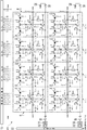
図2は、図1中の固体撮像素子4の概略構成を示す回路図である。図3は、図2中の列方向に順次並んだ4つの画素ブロックBLの付近を拡大して示す回路図である。図4は、図3中の3つの画素ブロックBLの付近を模式的に示す概略平面図である。図5は、図4中の1つの画素ブロックBLの付近を拡大して示す概略平面図である。本実施の形態では、固体撮像素子4は、CMOS型の固体撮像素子として構成されているが、これに限らず、例えば、他のXYアドレス型固体撮像素子として構成してもよい。
FIG. 2 is a circuit diagram showing a schematic configuration of the solid-
固体撮像素子4は、図2乃至図4に示すように、N行M列に2次元マトリクス状に配置されそれぞれ2つの画素PX(PXA,PXB)を有する画素ブロックBLと、後述する第1のノードPaとこれに対応する第2のノードPbとの間を電気的に接続及び切断する第1のスイッチ部としての第1のトランジスタSWAと、2つの第2のノードPb間を電気的に接続及び切断する第2のスイッチ部としての第2のトランジスタSWBと、第2のノードPbに所定電位としての電源電圧VDDを供給する第3のスイッチ部としてのリセットトランジスタRSTと、垂直走査回路21と、画素ブロックBLの行毎に設けられた制御線22〜27と、画素PXの列毎に(画素ブロックBLの列毎に)設けられ対応する列の画素PX(画素ブロックBL)からの信号を受け取る複数の(M本の)垂直信号線28と、各垂直信号線28に設けられた定電流源29と、各垂直信号線28に対応して設けられたカラムアンプ30、CDS回路(相関2重サンプリング回路)31及びA/D変換器32と、水平読み出し回路33とを有している。
As shown in FIGS. 2 to 4, the solid-
なお、カラムアンプ30として、アナログ増幅器を用いてもよいし、いわゆるスイッチトキャパシタアンプを用いてもよい。また、カラムアンプ30は、必ずしも設けなくてもよい。
As the
図面表記の便宜上、図2ではM=2として示しているが、列数Mは実際にはより多くの任意の数にされる。また、行数Nも限定されない。画素ブロックBLを行毎に区別する場合、j行目の画素ブロックBLは符号BL(j)で示す。この点は、他の要素や後述する制御信号についても同様である。図2及び図3には、4行に渡るn−1行目乃至n+2行目の画素ブロックBL(n−1)〜BL(n+2)が示されている。 For convenience of drawing notation, although it is shown as M = 2 in FIG. 2, the number of columns M is actually a larger arbitrary number. Further, the number of lines N is not limited. When the pixel block BL is distinguished for each row, the pixel block BL on the jth row is indicated by the reference numeral BL (j). This point also applies to other elements and control signals described later. 2 and 3 show pixel blocks BL (n-1) to BL (n + 2) in the n-1th row to the n + 2nd row over four rows.
なお、図面では、画素ブロックBLのうち図2及び図3中下側の画素の符号をPXAとし、図2及び図3中上側の画素の符号をPXBとして、両者を区別しているが、両者を区別しないで説明するときには両者に符号PXを付して説明する場合がある。また、図面では、画素PXAのフォトダイオードの符号をPDAとし、画素PXBのフォトダイオードの符号をPDBとして、両者を区別しているが、両者を区別しないで説明するときには両者に符号PDを付して説明する場合がある。同様に、画素PXAの転送トランジスタの符号をTXAとし、画素PXBの転送トランジスタの符号をTXBとして、両者を区別しているが、両者を区別しないで説明するときには両者に符号TXを付して説明する場合がある。なお、本実施の形態では、画素PXのフォトダイオードPDは、2N行M列に2次元マトリクス状に配置されている。 In the drawings, the reference numerals of the lower pixels in FIGS. 2 and 3 of the pixel block BL are referred to as PXA, and the reference numerals of the upper pixels in FIGS. 2 and 3 are referred to as PXB. When the explanation is made without distinction, both may be described by adding a reference numeral PX. Further, in the drawings, the code of the photodiode of the pixel PXA is PDA, and the code of the photodiode of the pixel PXB is PDB, and the two are distinguished. However, when the explanation is made without distinguishing between the two, the code PD is added to both. May be explained. Similarly, the code of the transfer transistor of the pixel PXA is TXA, and the code of the transfer transistor of the pixel PXB is TXB, and the two are distinguished. However, when the description is made without distinguishing between the two, the code TX is added to both. In some cases. In the present embodiment, the photodiode PDs of the pixels PX are arranged in a 2N row and M column in a two-dimensional matrix.
本実施の形態では、各画素PXは、入射光に応じた信号電荷を生成し蓄積する光電変換部としてのフォトダイオードPDと、フォトダイオードPDから第1のノードPaに電荷を転送する転送スイッチとしての転送トランジスタTXとを有している。 In the present embodiment, each pixel PX has a photodiode PD as a photoelectric conversion unit that generates and stores a signal charge according to the incident light, and a transfer switch that transfers the charge from the photodiode PD to the first node Pa. It has a transfer transistor TX of.
本実施の形態では、複数の画素PXは、フォトダイオードPDが列方向に順次並んだ2個の画素PX(PXA,PXB)毎に画素ブロックBLをなしている。図2及び図3に示すように、各画素ブロックBL毎に、当該画素ブロックBLに属する2個の画素PX(PXA,PXB)が、1組の第1のノードPa、増幅トランジスタAMP及び選択トランジスタSELを共有している。第1のノードPaには基準電位との間に容量(電荷電圧変換容量)が形成され、その容量によって、第1のノードPaに転送されてきた電荷が電圧に変換される。増幅トランジスタAMPは、第1のノードPaの電位に応じた信号を出力する増幅部を構成している。選択トランジスタSELは、当該画素ブロックBLを選択するための選択部を構成している。フォトダイオードPD及び転送トランジスタTXは、2個の画素PX(PXA,PXB)で共有されることなく、画素PX毎に設けられている。図2及び図3では、nは画素ブロックBLの行を示している。例えば、1行目の画素PX(PXA)と2行目の画素PX(PXB)とにより1行目の画素ブロックBLが構成され、3行目の画素PX(PXA)と4行目の画素PX(PXB)とにより2行目の画素ブロックBLが構成されている。 In the present embodiment, the plurality of pixels PX form a pixel block BL for each of two pixel PXs (PXA, PXB) in which photodiode PDs are sequentially arranged in the column direction. As shown in FIGS. 2 and 3, for each pixel block BL, two pixels PX (PXA, PXB) belonging to the pixel block BL form a set of a first node Pa, an amplification transistor AMP, and a selection transistor. Sharing SEL. A capacitance (charge-voltage conversion capacitance) is formed in the first node Pa with the reference potential, and the charge transferred to the first node Pa is converted into a voltage by the capacitance. The amplification transistor AMP constitutes an amplification unit that outputs a signal corresponding to the potential of the first node Pa. The selection transistor SEL constitutes a selection unit for selecting the pixel block BL. The photodiode PD and the transfer transistor TX are provided for each pixel PX without being shared by the two pixels PX (PXA, PXB). In FIGS. 2 and 3, n indicates a row of pixel block BL. For example, the pixel block BL in the first row is composed of the pixel PX (PXA) in the first row and the pixel PX (PXB) in the second row, and the pixel PX (PXA) in the third row and the pixel PX in the fourth row. (PXB) and the pixel block BL of the second row are configured.
例えば、画素ブロックBL(n)の転送トランジスタTXA(n)は、フォトダイオードPDA(n)から第1のノードPa(n)に電荷を転送し、転送トランジスタTXB(n)はフォトダイオードPDB(n)から第1のノードPa(n)に電荷を転送する。第1のノードPa(n)には基準電位との間に容量(電荷電圧変換容量)が形成され、その容量によって、第1のノードPa(n)に転送されてきた電荷が電圧に変換される。増幅トランジスタAMP(n)は、第1のノードPa(n)の電位に応じた信号を出力する。これらの点は、他の画素ブロックBLの行についても同様である。 For example, the transfer transistor TXA (n) of the pixel block BL (n) transfers an electric charge from the photodiode PDA (n) to the first node Pa (n), and the transfer transistor TXB (n) is the photodiode PDB (n). ) To the first node Pa (n). A capacitance (charge-voltage conversion capacitance) is formed in the first node Pa (n) with the reference potential, and the charge transferred to the first node Pa (n) is converted into a voltage by the capacitance. To. The amplification transistor AMP (n) outputs a signal corresponding to the potential of the first node Pa (n). These points are the same for the rows of other pixel blocks BL.
なお、本発明では、例えば、フォトダイオードPDが列方向に順次並んだ3個以上の画素PX毎に画素ブロックBLを構成するようにしてもよい。 In the present invention, for example, the pixel block BL may be configured for each of three or more pixel PXs in which the photodiode PDs are sequentially arranged in the column direction.
図面には示していないが、本実施の形態では、各々の画素PXのフォトダイオードPDの光入射側には、それぞれが異なる色成分の光を透過させる複数種類のカラーフィルタが、所定の色配列(例えば、ベイヤー配列)で配置されている。画素PXは、カラーフィルタでの色分解によって各色に対応する電気信号を出力する。 Although not shown in the drawings, in the present embodiment, a plurality of types of color filters that transmit light having different color components are arranged in a predetermined color arrangement on the light incident side of the photodiode PD of each pixel PX. (For example, Bayer arrangement). The pixel PX outputs an electric signal corresponding to each color by color separation by a color filter.
第1のトランジスタSWA(n)は、第1のノードPa(n)とこれに対応する第2のノードPb(n)との間を電気的に接続及び切断する第1のスイッチ部を構成している。このような第1のスイッチ部は、複数のトランジスタ等のスイッチを組み合わせて構成することも可能であるが、構造を簡単にするため、本実施の形態のように単一の第1のトランジスタSWA(n)で構成することが好ましい。これらの点は、他の第1のトランジスタSWAについても同様である。 The first transistor SWA (n) constitutes a first switch unit that electrically connects and disconnects between the first node Pa (n) and the corresponding second node Pb (n). ing. Such a first switch unit can be configured by combining switches such as a plurality of transistors, but in order to simplify the structure, a single first transistor SWA as in the present embodiment. It is preferably composed of (n). These points are the same for the other first transistor SWA.
各第2のトランジスタSWBは、各画素ブロックBLのうちの列方向に互いに隣り合う各2つの画素ブロックBLについて、一方の画素ブロックBLの第1のノードPaに対応する第2のノードPbと他方の画素ブロックBLの第1のノードPaに対応する第2のノードPbとの間を電気的に接続及び切断するように設けられた第2のスイッチ部を構成している。これによって、本実施の形態では、3つ以上の画素ブロックBLの第1のノードPaが、複数の前記第2のスイッチ部により数珠繋ぎ状に接続されている。前述したような第2のスイッチ部は、複数のトランジスタ等のスイッチを組み合わせて構成することも可能であるが、構造を簡単にするため、本実施の形態のように単一の第2のトランジスタSWBで構成することが好ましい。 Each second transistor SWB is a second node Pb corresponding to the first node Pa of one pixel block BL and the other for each of two pixel blocks BL adjacent to each other in the column direction of each pixel block BL. A second switch unit is configured so as to electrically connect and disconnect from the second node Pb corresponding to the first node Pa of the pixel block BL of the above. As a result, in the present embodiment, the first node Pa of the three or more pixel blocks BL is connected in a string by the plurality of second switch portions. The second switch unit as described above can be configured by combining switches such as a plurality of transistors, but in order to simplify the structure, a single second transistor as in the present embodiment. It is preferably composed of SWB.
例えば、第2のトランジスタSWB(n)は、n行目の画素ブロックBL(n)の第1のノードPa(n)に対応する第2のノードPb(n)とn−1行目の画素ブロックBL(n−1)の第1のノードPa(n−1)に対応する第2のノードPb(n−1)との間を電気的に接続及び切断するように、設けられている。この点は、他の第2のトランジスタSWBについても同様である。 For example, the second transistor SWB (n) is the second node Pb (n) corresponding to the first node Pa (n) of the pixel block BL (n) in the nth row and the pixels in the n-1th row. It is provided so as to electrically connect and disconnect from the second node Pb (n-1) corresponding to the first node Pa (n-1) of the block BL (n-1). This point is the same for the other second transistor SWB.
リセットトランジスタRST(n)は、第2のノードPb(n)に所定電位としての電源電圧VDDを供給する第3のスイッチ部を構成している。このような第3のスイッチ部は、複数のトランジスタ等のスイッチを組み合わせて構成することも可能であるが、構造を簡単にするため、本実施の形態のように単一のリセットトランジスタRST(n)で構成することが好ましい。これらの点は、他のリセットトランジスタRSTについても同様である。 The reset transistor RST (n) constitutes a third switch unit that supplies the power supply voltage VDD as a predetermined potential to the second node Pb (n). Such a third switch unit can be configured by combining switches such as a plurality of transistors, but in order to simplify the structure, a single reset transistor RST (n) as in the present embodiment. ) Is preferable. These points are the same for other reset transistors RST.
図2及び図3において、VDDは電源電位である。なお、本実施の形態では、トランジスタTXA,TXB,AMP,RST,SEL,SWA,SWBは、全てnMOSトランジスタである。 In FIGS. 2 and 3, VDD is the power supply potential. In the present embodiment, the transistors TXA, TXB, AMP, RST, SEL, SWA, and SWB are all nMOS transistors.
転送トランジスタTXAのゲートは行毎に制御線26に共通に接続され、そこには、制御信号φTXAが垂直走査回路21から供給される。転送トランジスタTXBのゲートは行毎に制御線25に共通に接続され、そこには、制御信号φTXBが垂直走査回路21から供給される。リセットトランジスタRSTのゲートは行毎に制御線24に共通に接続され、そこには、制御信号φRSTが垂直走査回路21から供給される。選択トランジスタSELのゲートは行毎に制御線23に共通に接続され、そこには、制御信号φSELが垂直走査回路21から供給される。第1のトランジスタSWAのゲートは行毎に制御線22に共通に接続され、そこには、制御信号φSWAが垂直走査回路21から供給される。第2のトランジスタSWBのゲートは行毎に制御線27に共通に接続され、そこには、制御信号φSWBが垂直走査回路21から供給される。例えば、転送トランジスタTXA(n)のゲートには制御信号φTXA(n)が供給され、転送トランジスタTXB(n)のゲートには制御信号φTXB(n)が供給され、リセットトランジスタRST(n)のゲートには制御信号φRST(n)が供給され、選択トランジスタSEL(n)のゲートには制御信号φSEL(n)が供給され、第1のトランジスタSWA(n)のゲートには制御信号φSWA(n)が供給され、第2のトランジスタSWB(n)のゲートには制御信号φSWB(n)が供給される。
The gate of the transfer transistor TXA is commonly connected to the
各トランジスタTXA,TXB,RST,SEL,SWA,SWBは、対応する制御信号φTXA,φTXB,φRST,φSEL,φSWA,φSWBがハイレベル(H)のときにオンし、ローレベル(L)のときにオフする。 Each transistor TXA, TXB, RST, SEL, SWA, SWB is turned on when the corresponding control signals φTXA, φTXB, φRST, φSEL, φSWA, φSWB are high level (H), and when the corresponding control signals are low level (L). Turn off.
垂直走査回路21は、図1中の撮像制御部5による制御下で、画素ブロックBLの行毎に、制御信号φTXA,φTXB,φRST,φSEL,φSWA,φSWBをそれぞれ出力し、画素ブロックBL、第1のトランジスタSWA、第2のトランジスタSWBを制御し、静止画読み出し動作や動画読み出し動作などを実現する。この制御において、例えばISO感度の設定値に応じて、後述する各動作モードの読み出し動作が行われる。この制御によって、各垂直信号線28には、それに対応する列の画素PXの信号(アナログ信号)が供給される。
Under the control of the image
本実施の形態では、垂直走査回路21は、後述する各動作モードを、図1中の撮像制御部5からの指令(制御信号)に応じて切り替えて行う制御部を構成している。
In the present embodiment, the
垂直信号線28に読み出された信号は、各列毎に、カラムアンプ30で増幅され更にCDS回路31にて光信号(画素PXで光電変換された光情報を含む信号)と暗信号(光信号から差し引くべきノイズ成分を含む差分用信号)との差分を得る処理が施された後に、A/D変換器32にてデジタル信号に変換され、そのデジタル信号はA/D変換器32に保持される。各A/D変換器32に保持されたデジタルの画像信号は、水平読み出し回路33によって水平走査され、必要に応じて所定の信号形式に変換されて、外部(図1中のデジタル信号処理部6)へ出力される。
The signal read out on the
なお、CDS回路31は、図1中の撮像制御部5による制御下でタイミング発生回路(図示せず)から暗信号サンプリング信号φDARKCを受け、φDARKCがハイレベル(H)の場合にカラムアンプ30の出力信号を暗信号としてサンプリングするとともに、図1中の撮像制御部5による制御下で前記タイミング発生回路から光信号サンプリング信号φSIGCを受け、φSIGCがHの場合にカラムアンプ30の出力信号を光信号としてサンプリングする。そして、CDS回路31は、前記タイミング発生回路からのクロックやパルスに基づいて、サンプリングした暗信号と光信号との差分に応じた信号を出力する。このようなCDS回路31の構成としては、公知の構成を採用することができる。
The
ここで、図4及び図5を参照して、画素ブロックBLの構造について説明する。実際には、フォトダイオードPDの上部にはカラーフィルタやマイクロレンズ等が配置されるが、図4及び図5では省略している。なお、図4及び図5において、電源線、グランド線及び制御線22〜27等のレイアウトは省略している。
Here, the structure of the pixel block BL will be described with reference to FIGS. 4 and 5. Actually, a color filter, a microlens, etc. are arranged on the upper part of the photodiode PD, but they are omitted in FIGS. 4 and 5. In addition, in FIGS. 4 and 5, the layout of the power supply line, the ground line, the
本実施の形態では、N型シリコン基板(図示せず)上にP型ウエル(図示せず)が設けられ、前記P型ウエル中にフォトダイオードPDなどの画素ブロックBLにおける各素子が配置されている。図5において、符号41〜50は、前述した各トランジスタの一部となっているN型不純物拡散領域である。符号61〜67は、ポリシリコンによる各トランジスタのゲート電極である。なお、拡散領域42,50は、図示しない電源線により電源電圧VDDが印加される領域である。
In the present embodiment, a P-type well (not shown) is provided on an N-type silicon substrate (not shown), and each element in the pixel block BL such as a photodiode PD is arranged in the P-type well. There is. In FIG. 5, reference numerals 41 to 50 are N-type impurity diffusion regions that are a part of each of the above-mentioned transistors.
フォトダイオードPDA(n),PDB(n)は、前記P型ウエル中に設けられたN型の電荷蓄積層(図示せず)とその表面側に配置されたP型の空乏化防止層(図示せず)からなる埋め込み型フォトダイオードである。フォトダイオードPDA(n),PDB(n)は、入射する光を光電変換し、生じた電荷をその電荷蓄積層に蓄積する。 The photodiodes PDA (n) and PDB (n) are an N-type charge storage layer (not shown) provided in the P-type well and a P-type depletion prevention layer (not shown) arranged on the surface side thereof (FIG.). It is an embedded photodiode consisting of (not shown). The photodiodes PDA (n) and PDB (n) photoelectrically convert incident light and accumulate the generated charge in the charge storage layer.
転送トランジスタTXA(n)は、フォトダイオードPDA(n)の電荷蓄積層をソース、拡散領域41をドレイン、ゲート電極61をゲートとするnMOSトランジスタである。転送トランジスタTXB(n)は、フォトダイオードPDB(n)の電荷蓄積層をソース、拡散領域41をドレイン、ゲート電極62をゲートとするnMOSトランジスタである。拡散領域41は、フォトダイオードPDA(n)とフォトダイオードPDB(n)との間に設けられている。拡散領域41は、転送トランジスタTXA(n)のドレインとなる拡散領域及び転送トランジスタTXB(n)のドレインとなる拡散領域として、兼用されている。転送トランジスタTXA(n)のゲート電極61は、拡散領域41のフォトダイオードPDA(n)側に配置されている。転送トランジスタTXB(n)のゲート電極62は、拡散領域41のフォトダイオードPDB(n)側に配置されている。
The transfer transistor TXA (n) is an nMOS transistor having the charge storage layer of the photodiode PDA (n) as the source, the diffusion region 41 as the drain, and the
増幅トランジスタAMP(n)は、拡散領域42をドレイン、拡散領域43をソース、ゲート電極63をゲートとするnMOSトランジスタである。選択トランジスタSEL(n)は、拡散領域43をドレイン、拡散領域44をソース、ゲート電極64をゲートとするnMOSトランジスタである。拡散領域44は、垂直信号線28に接続されている。
The amplification transistor AMP (n) is an nMOS transistor having a
第1のトランジスタSWA(n)は、拡散領域45をソース、拡散領域46をドレイン、ゲート電極65をゲートとするnMOSトランジスタである。第2のトランジスタSWB(n)は、拡散領域47をドレイン、拡散領域48をソース、ゲート電極66をゲートとするnMOSトランジスタである。リセットトランジスタRST(n)は、拡散領域49をソース、拡散領域50をドレイン、ゲート電極67をゲートとするnMOSトランジスタである。
The first transistor SWA (n) is an nMOS transistor having a
画素ブロックBL(n)のゲート電極63及び拡散領域41,45間が、配線71(n)によって互いに電気的に接続されて導通している。本実施の形態では、第1のノードPa(n)は、配線71(n)及びこれに対して電気的に接続されて導通している箇所全体に相当している。
The
第1のトランジスタSWA(n)のドレイン拡散領域46、第2のトランジスタSWB(n)のドレイン拡散領域47、リセットトランジスタRST(n)のソース拡散領域49及び第2のトランジスタSWB(n+1)のソース拡散領域48の間が、配線72(n)によって互いに電気的に接続されて導通している。第2のノードPb(n)は、配線72(n)及びこれに対して電気的に接続されて導通している箇所全体に相当している。これらの点は、他の第1のトランジスタSWA、他の第2のトランジスタSWB及び他のリセットトランジスタRSTについても同様である。
Drain diffusion region 46 of the first transistor SWA (n),
n行目以外の画素ブロックBLの構造も、前述したn行目の画素ブロックBL(n)の構造と同様である。第1のトランジスタSWA(n)以外の第1のトランジスタSWAの構造も、前述した第1のトランジスタSWA(n)の構造と同様である。第2のトランジスタSWB(n)以外の連結トランジスタSWBの構造も、前述した連結トランジスタSWB(n)の構造と同様である。リセットトランジスタRST(n)以外のリセットトランジスタRSTの構造も、前述したリセットトランジスタRST(n)の構造と同様である。 The structure of the pixel block BL other than the nth row is the same as the structure of the pixel block BL (n) of the nth row described above. The structure of the first transistor SWA other than the first transistor SWA (n) is the same as the structure of the first transistor SWA (n) described above. The structure of the connected transistor SWB other than the second transistor SWB (n) is the same as the structure of the connected transistor SWB (n) described above. The structure of the reset transistor RST other than the reset transistor RST (n) is the same as the structure of the reset transistor RST (n) described above.
図2乃至図5おいて、CC(n)は、第1のトランジスタSWA(n)がオフしている場合の、第1のノードPa(n)と基準電位との間の容量である。容量CC(n)の容量値をCfd1とする。CD(n)は、第1のトランジスタSWA(n)、第2のトランジスタSWB(n),SWB(n+1)及びリセットトランジスタRST(n)がオフしている場合の、配線72(n)と基準電位との間の容量である。容量CD(n)の容量値をCfd2とする。これらの点は、他の第1のトランジスタSWA、他の第2のトランジスタSWB及び他のリセットトランジスタRSTについても同様である。 In FIGS. 2 to 5, CC (n) is the capacitance between the first node Pa (n) and the reference potential when the first transistor SWA (n) is off. Let the capacitance value of the capacitance CC (n) be Cfd1. The CD (n) is the wiring 72 (n) and the reference when the first transistor SWA (n), the second transistor SWB (n), SWB (n + 1) and the reset transistor RST (n) are off. The capacitance between the potential. The capacity value of the capacity CD (n) is Cfd2. These points are the same for the other first transistor SWA, the other second transistor SWB, and the other reset transistor RST.
容量CC(n)は、転送トランジスタTXA(n),TXB(n)のドレイン拡散領域41の容量と、第1のトランジスタSWA(n)のソース拡散領域の容量と、増幅トランジスタAMP(n)のゲート電極63の容量と、配線71(n)の配線容量とから構成され、それらの容量値の合計が容量CC(n)の容量値Cfd1となる。この点は、他の画素ブロックBLの行についても同様である。なお、第2のトランジスタSWB(n)のドレイン拡散領域47及びリセットトランジスタRST(n)のソース拡散領域49は容量CC(n)の構成要素とならないので、その分、容量CC(n)の容量値Cfd1は小さくなる。
The capacitance CC (n) is the capacitance of the drain diffusion region 41 of the transfer transistors TXA (n) and TXB (n), the capacitance of the source diffusion region of the first transistor SWA (n), and the amplification transistor AMP (n). It is composed of the capacitance of the
ここで、第1のトランジスタSWAのオン時のチャネル容量の値及び第2のトランジスタSWBのオン時のチャネル容量の値を、両方ともCswとする。通常、容量値Cswは、容量値Cfd1,Cfd2に対して小さい値である。 Here, the value of the channel capacitance when the first transistor SWA is ON and the value of the channel capacitance when the second transistor SWB is ON are both set to Csw. Usually, the capacitance value Csw is a small value with respect to the capacitance values Cfd1 and Cfd2.
今、画素ブロックBL(n)に着目して、第1のトランジスタSWA(n)がオフする(すなわち、各第1のトランジスタSWA及び各第2のトランジスタSWBのうちのオン状態のトランジスタが第1のノードPa(n)に対して電気的に接続された状態とならない)と、第1のノードPa(n)と基準電位との間の容量(電荷電圧変換容量)は、容量CC(n)となる。よって、第1のノードPa(n)の電荷電圧変換容量の容量値は、Cfd1となる。この状態は、後述する第1の動作モードを示す図6中の期間T2中の第1のノードPa(n)のリセット時以外の状態(図6中の期間T2においてφSWA(n)がLの期間の状態)に相当している。 Now, focusing on the pixel block BL (n), the first transistor SWA (n) is turned off (that is, the on-state transistor of each first transistor SWA and each second transistor SWB is the first. The capacitance (charge-voltage conversion capacitance) between the first node Pa (n) and the reference potential is the capacitance CC (n). It becomes. Therefore, the capacitance value of the charge-voltage conversion capacitance of the first node Pa (n) is Cfd1. This state is a state other than the time when the first node Pa (n) in the period T2 in FIG. 6 showing the first operation mode described later is reset (φSWA (n) is L in the period T2 in FIG. 6). It corresponds to the state of the period).
また、画素ブロックBL(n)に着目して、第1のトランジスタSWA(n)がオンすると、各第1のトランジスタSWA及び各第2のトランジスタSWBのうち、第1のトランジスタSWA(n)以外のオン状態のトランジスタが第1のノードPa(n)に対して電気的に接続された状態とならなければ(ここでは、具体的には、第2のトランジスタSWB(n),SWB(n+1)がオフであれば)、第1のノードPa(n)と基準電位との間の容量(電荷電圧変換容量)は、容量CC(n)に対して、容量CD(n)及び第1のトランジスタSWA(n)のオン時のチャネル容量を付加したものとなる。よって、第1のノードPa(n)の電荷電圧変換容量の容量値は、Cfd1+Cfd2+Csw≒Cfd1+Cfd2となる。この状態は、後述する第2の動作モードを示す図7中の期間T2の状態に相当している。 Further, paying attention to the pixel block BL (n), when the first transistor SWA (n) is turned on, among the first transistor SWA and each second transistor SWB, other than the first transistor SWA (n). Unless the on-state transistor is electrically connected to the first node Pa (n) (specifically, here, the second transistors SWB (n), SWB (n + 1)). (If is off), the capacitance (charge-voltage conversion capacitance) between the first node Pa (n) and the reference potential is the capacitance CD (n) and the first transistor with respect to the capacitance CC (n). The channel capacitance when SWA (n) is on is added. Therefore, the capacitance value of the charge-voltage conversion capacitance of the first node Pa (n) is Cfd1 + Cfd2 + Csw≈Cfd1 + Cfd2. This state corresponds to the state of the period T2 in FIG. 7 showing the second operation mode described later.
さらに、画素ブロックBL(n)に着目して、第1のトランジスタSWA(n)及び第2のトランジスタSWB(n+1)がオンすると、各第1のトランジスタSWA及び各第2のトランジスタSWBのうち、トランジスタSWA(n),SWB(n+1)以外のオン状態のトランジスタが第1のノードPa(n)に対して電気的に接続された状態とならなければ(ここでは、具体的には、トランジスタSWB(n),SWA(n+1),SWB(n+2)がオフであれば)、第1のノードPa(n)の電荷電圧変換容量は、容量CC(n)に対して、容量CD(n)、容量CD(n+1)及びトランジスタSWA(n),SWB(n+1)のオン時のチャネル容量を付加したものとなる。よって、第1のノードPa(n)の電荷電圧変換容量の容量値は、Cfd1+2×Cfd2+2×Csw≒Cfd1+2×Cfd2となる。この状態は、後述する第3Aの動作モードを示す図8中の期間T2の状態に相当している。 Further, focusing on the pixel block BL (n), when the first transistor SWA (n) and the second transistor SWB (n + 1) are turned on, among the first transistor SWA and each second transistor SWB, Unless the on-state transistors other than the transistors SWA (n) and SWB (n + 1) are electrically connected to the first node Pa (n) (here, specifically, the transistor SWB). (If (n), SWA (n + 1), SWB (n + 2) are off), the charge-voltage conversion capacitance of the first node Pa (n) is the capacitance CD (n) with respect to the capacitance CC (n). The channel capacitance when the capacitance CD (n + 1) and the transistors SWA (n) and SWB (n + 1) are on is added. Therefore, the capacitance value of the charge-voltage conversion capacitance of the first node Pa (n) is Cfd1 + 2 × Cfd2 + 2 × Csw≈Cfd1 + 2 × Cfd2. This state corresponds to the state of the period T2 in FIG. 8 showing the operation mode of the third A described later.
さらにまた、画素ブロックBL(n)に着目して、第1のトランジスタSWA(n),SWA(n+1)及び第2のトランジスタSWB(n+1)がオンすると、各第1のトランジスタSWA及び各第2のトランジスタSWBのうち、トランジスタSWA(n),SWA(n+1),SWB(n+1)以外のオン状態のトランジスタが第1のノードPa(n)に対して電気的に接続された状態とならなければ(ここでは、具体的には、トランジスタSWB(n),SWB(n+2)がオフであれば)、第1のノードPa(n)の電荷電圧変換容量は、容量CC(n)に対して、容量CD(n)、容量CD(n+1)、容量CC(n+1)及びトランジスタSWA(n),SWA(n+1),SWB(n+1)のオン時のチャネル容量を付加したものとなる。よって、第1のノードPa(n)の電荷電圧変換容量の容量値は、2×Cfd1+2×Cfd2+3×Csw≒2×Cfd1+2×Cfd2となる。この状態は、後述する第3Bの動作モードを示す図9中の期間T2の状態に相当している。 Furthermore, focusing on the pixel block BL (n), when the first transistors SWA (n), SWA (n + 1) and the second transistor SWB (n + 1) are turned on, each first transistor SWA and each second transistor are turned on. Among the transistors SWB in the above, unless the on-state transistors other than the transistors SWA (n), SWA (n + 1), and SWB (n + 1) are electrically connected to the first node Pa (n). (Specifically, if the transistors SWB (n) and SWB (n + 2) are off), the charge-voltage conversion capacitance of the first node Pa (n) is relative to the capacitance CC (n). The channel capacitances of the capacitance CD (n), the capacitance CD (n + 1), the capacitance CC (n + 1), and the transistors SWA (n), SWA (n + 1), and SWB (n + 1) at the time of on are added. Therefore, the capacitance value of the charge-voltage conversion capacitance of the first node Pa (n) is 2 × Cfd1 + 2 × Cfd2 + 3 × Csw≈2 × Cfd1 + 2 × Cfd2. This state corresponds to the state of the period T2 in FIG. 9, which shows the operation mode of the third B described later.
また、画素ブロックBL(n)に着目して、第1のトランジスタSWA(n)及び第2のトランジスタSWB(n+1),SWB(n+2)がオンすると、各第1のトランジスタSWA及び各第2のトランジスタSWBのうち、トランジスタSWA(n),SWB(n+1),SWB(n+2)以外のオン状態のトランジスタが第1のノードPa(n)に対して電気的に接続された状態とならなければ(ここでは、具体的には、トランジスタSWA(n+1),SWA(n+2),SWB(n),SWB(n+3)がオフであれば)、第1のノードPa(n)の電荷電圧変換容量は、容量CC(n)に対して、容量CD(n)、容量CD(n+1)、容量CD(n+2)及びトランジスタSWA(n),SWB(n+1),SWB(n+2)のオン時のチャネル容量を付加したものとなる。よって、第1のノードPa(n)の電荷電圧変換容量の容量値は、Cfd1+3×Cfd2+3×Csw≒Cfd1+3×Cfd2となる。この状態は、後述する第3Cの動作モードを示す図10中の期間T2の状態に相当している。 Further, paying attention to the pixel block BL (n), when the first transistor SWA (n) and the second transistors SWB (n + 1) and SWB (n + 2) are turned on, each of the first transistor SWA and each second transistor is turned on. Of the transistors SWB, on-state transistors other than the transistors SWA (n), SWB (n + 1), and SWB (n + 2) must be electrically connected to the first node Pa (n) ( Here, specifically, if the transistors SWA (n + 1), SWA (n + 2), SWB (n), and SWB (n + 3) are off), the charge-voltage conversion capacitance of the first node Pa (n) is Addition of channel capacitance when the capacitance CD (n), capacitance CD (n + 1), capacitance CD (n + 2) and transistors SWA (n), SWB (n + 1), SWB (n + 2) are turned on to the capacitance CC (n). It will be the one that was done. Therefore, the capacitance value of the charge-voltage conversion capacitance of the first node Pa (n) is Cfd1 + 3 × Cfd2 + 3 × Csw≈Cfd1 + 3 × Cfd2. This state corresponds to the state of the period T2 in FIG. 10 showing the operation mode of the third C described later.
このように、各第1のトランジスタSWA及び各第2のトランジスタSWBのうち第1のノードPa(n)に対して電気的に接続されるオン状態のトランジスタがなければ、第1のノードPa(n)の電荷電圧変換容量の容量値が最小の容量値Cfd1となり、その電荷電圧変換容量による電荷電圧変換係数が大きくなるため、最高のSN比での読出しが可能となる。 As described above, if there is no on-state transistor electrically connected to the first node Pa (n) among the first transistor SWA and each second transistor SWB, the first node Pa ( Since the capacity value of the charge-voltage conversion capacity of n) becomes the minimum capacity value Cfd1 and the charge-voltage conversion coefficient due to the charge-voltage conversion capacity becomes large, it is possible to read at the highest SN ratio.
一方、各第1のトランジスタSWA及び各第2のトランジスタSWBのうち第1のノードPa(n)に対して電気的に接続されるオン状態のトランジスタの数を1つ以上の所望の数に増やしていけば、第1のノードPa(n)の電荷電圧変換容量の容量値を所望の値に大きくすることができ、大きな信号電荷量を扱うことができるため、飽和電子数を拡大することができる。これにより、ダイナミックレンジを拡大することができる。 On the other hand, among the first transistor SWA and each second transistor SWB, the number of on-state transistors electrically connected to the first node Pa (n) is increased to one or more desired number. As a result, the capacitance value of the charge-voltage conversion capacitance of the first node Pa (n) can be increased to a desired value, and a large signal charge amount can be handled, so that the number of saturated electrons can be increased. it can. As a result, the dynamic range can be expanded.
以上、画素ブロックBL(n)の第1のノードPa(n)について説明したが、他の画素ブロックBLの第1のノードPaについても同様である。 The first node Pa (n) of the pixel block BL (n) has been described above, but the same applies to the first node Pa (n) of the other pixel block BL.
図6は、図2に示す固体撮像素子4の第1の動作モードを示すタイミングチャートである。この第1の動作モードは、各画素ブロックBLを行毎に順次選択していき、各第1のトランジスタSWA及び各第2のトランジスタSWBのうち選択された画素ブロックBLの第1のノードPaに対して電気的に接続されるオン状態のトランジスタがない状態(当該第1のノードPaの電荷電圧変換容量が最小である状態)で、選択された画素ブロックBLの転送トランジスタTXA,TXBを順次選択的にオンさせて、選択された画素ブロックBLの各フォトダイオードPDA,PDBの信号を行毎に順次読み出す動作の例である。図6に示す例では、全画素PXA,PXBの信号を読み出すが、これに限らず、例えば、画素行を間引いて読み出す間引き読み出し等を行ってもよい。この点は、後述する図7乃至図10にそれぞれ示す各例についても同様である。
FIG. 6 is a timing chart showing the first operation mode of the solid-
図6は、期間T1においてn−1行目の画素ブロックBL(n−1)が選択され、期間T2においてn行目の画素ブロックBL(n)が選択され、期間T3においてn+1行目の画素ブロックBL(n+1)が選択されていく状況を示している。いずれの行の画素ブロックBLが選択された場合の動作も同様であるので、ここでは、n行目の画素ブロックBL(n)が選択された場合の動作についてのみ説明する。 In FIG. 6, the pixel block BL (n-1) in the n-1th row is selected in the period T1, the pixel block BL (n) in the nth row is selected in the period T2, and the pixels in the n + 1th row in the period T3. It shows the situation where the block BL (n + 1) is selected. Since the operation when the pixel block BL of any row is selected is the same, only the operation when the pixel block BL (n) of the nth row is selected will be described here.
期間T2の開始前に既に、所定の露光期間において、フォトダイオードPDA(n),PDB(n)の露光が終了している。この露光は、通常の本撮影時(静止画撮影時)などでは、全画素を同時にリセットするいわゆるグローバルリセット後にメカニカルシャッタ(図示せず)により行われ、電子ビューファインダーモード時や動画撮影時などでは、いわゆるローリング電子シャッタ動作により行われる。期間T2の開始直前には、全てのトランジスタSEL,RST,TXA,TXB,SWA,SWBはオフしている。 The exposure of the photodiodes PDA (n) and PDB (n) has already been completed in the predetermined exposure period before the start of the period T2. This exposure is performed by a mechanical shutter (not shown) after a so-called global reset that resets all pixels at the same time during normal main shooting (still image shooting), and in electronic viewfinder mode or movie shooting. , So-called rolling electronic shutter operation. Immediately before the start of period T2, all transistors SEL, RST, TXA, TXB, SWA, and SWB are turned off.
期間T2において、n行目のφSEL(n)がHにされ、n行目の画素ブロックBL(n)の選択トランジスタSEL(n)がオンにされ、n行目の画素ブロックBL(n)が選択される。また、期間T2において、n行目のφRST(n)がHにされ、リセットトランジスタRST(n)がオンにされる。もっとも、リセットトランジスタRST(n)は必ずしも期間T2の全体に渡ってオンにする必要はなく、φRST(n)は、第1のノードPa(n)のリセット時(すなわち、図6中のφSWA(n)のH期間)のみHにしてもよい。 In the period T2, φSEL (n) in the nth row is set to H, the selection transistor SEL (n) in the pixel block BL (n) in the nth row is turned on, and the pixel block BL (n) in the nth row is changed. Be selected. Further, in the period T2, φRST (n) on the nth row is set to H, and the reset transistor RST (n) is turned on. However, the reset transistor RST (n) does not necessarily have to be turned on for the entire period T2, and φRST (n) is when the first node Pa (n) is reset (that is, φSWA (that is, φSWA) in FIG. Only the H period) of n) may be set to H.
期間T2の開始直後から一定期間(第1のノードPa(n)のリセット時)だけ、φSWA(n)がHにされてn行目の第1のトランジスタSWA(n)が一旦オンにされる。このとき、φRST(n)がHにされていてリセットトランジスタRST(n)がオンしているため、オン状態のリセットトランジスタRST(n)及びオン状態の第1のトランジスタSWA(n)を経由して、第1のノードPa(n)の電位が一旦電源電位VDDにリセットされる。 ΦSWA (n) is set to H and the first transistor SWA (n) on the nth row is temporarily turned on for a certain period (when the first node Pa (n) is reset) immediately after the start of the period T2. .. At this time, since φRST (n) is set to H and the reset transistor RST (n) is on, the reset transistor RST (n) in the on state and the first transistor SWA (n) in the on state are passed through. Then, the potential of the first node Pa (n) is once reset to the power supply potential VDD.
その後、第1のトランジスタSWA(n)がオフにされると、各トランジスタSWA,SWBのうち選択された画素ブロックBL(n)の第1のノードPa(n)に対して電気的に接続されるオン状態のトランジスタがない状態となる。したがって、前述したように、第1のノードPa(n)の電荷電圧変換容量の容量値は、Cfd1となり、最小となる。 After that, when the first transistor SWA (n) is turned off, it is electrically connected to the first node Pa (n) of the pixel block BL (n) selected from the transistors SWA and SWB. There is no transistor in the on state. Therefore, as described above, the capacitance value of the charge-voltage conversion capacitance of the first node Pa (n) is Cfd1, which is the minimum.
期間T2中のその後の時点t1から一定期間だけ、暗信号サンプリング信号φDARKCがHにされて、第1のノードPa(n)に現れる電位がn行目の増幅トランジスタAMP(n)で増幅された後に選択トランジスタSEL(n)及び垂直信号線28を経由し更にカラムアンプ30で増幅された信号が、暗信号として、CDS回路31によりサンプリングされる。
The dark signal sampling signal φDARKC was set to H for a certain period from the subsequent time point t1 during the period T2, and the potential appearing at the first node Pa (n) was amplified by the amplification transistor AMP (n) on the nth row. Later, the signal further amplified by the
期間T2中のその後の時点t2から一定期間だけ、φTXA(n)がHにされてn行目の転送トランジスタTXA(n)がオンにされる。これにより、n行目の画素ブロックBL(n)のフォトダイオードPDA(n)に蓄積されていた信号電荷が、第1のノードPa(n)の電荷電圧変換容量に転送される。第1のノードPa(n)の電位は、ノイズ成分を除くと、この信号電荷の量と第1のノードPa(n)の電荷電圧変換容量の容量値の逆数とに比例した値となる。 For a certain period from the subsequent time point t2 in the period T2, φTXA (n) is set to H and the transfer transistor TXA (n) on the nth row is turned on. As a result, the signal charge stored in the photodiode PDA (n) of the pixel block BL (n) on the nth row is transferred to the charge-voltage conversion capacitance of the first node Pa (n). The potential of the first node Pa (n) is a value proportional to the amount of this signal charge and the reciprocal of the capacitance value of the charge voltage conversion capacitance of the first node Pa (n), excluding the noise component.
期間T2中のその後の時点t3において、光信号サンプリング信号φSIGCがHにされて、第1のノードPa(n)に現れる電位がn行目の増幅トランジスタAMP(n)で増幅された後に選択トランジスタSEL(n)及び垂直信号線28を経由し更にカラムアンプ30で増幅された信号が、光信号として、CDS回路31によりサンプリングされる。
At the subsequent time point t3 during the period T2, the optical signal sampling signal φSIGC is set to H, and the potential appearing at the first node Pa (n) is amplified by the amplification transistor AMP (n) in the nth row, and then the selection transistor. The signal further amplified by the
その後にφSIGCがLになった時点の後に、CDS回路31は、時点t1からの一定期間でサンプリングした暗信号と時点t3からの一定時間でサンプリングした光信号との差分に応じた信号を出力する。A/D変換器32は、この差分に応じた信号をデジタル信号に変換して保持する。各A/D変換器32に保持されたデジタルの画像信号は、水平読み出し回路33によって水平走査され、デジタル信号画像信号として外部(図1中のデジタル信号処理部6)へ出力される。
After that, after the time when φSIGC becomes L, the
そして、期間T2中の時点t4から一定期間(第1のノードPa(n)のリセット時)だけ、φSWA(n)がHにされてn行目の第1のトランジスタSWA(n)が一旦オンにされる。このとき、φSEL(n)がHにされていてリセットトランジスタRST(n)がオンしているため、オン状態のリセットトランジスタRST(n)及びオン状態の第1のトランジスタSWA(n)を経由して、第1のノードPa(n)の電位が一旦電源電位VDDにリセットされる。 Then, φSWA (n) is set to H and the first transistor SWA (n) on the nth row is turned on once for a certain period (when the first node Pa (n) is reset) from the time point t4 in the period T2. To be reset. At this time, since φSEL (n) is set to H and the reset transistor RST (n) is on, the reset transistor RST (n) in the on state and the first transistor SWA (n) in the on state are passed through. Then, the potential of the first node Pa (n) is once reset to the power supply potential VDD.
その後、第1のトランジスタSWA(n)がオフにされると、各トランジスタSWA,SWBのうち選択された画素ブロックBL(n)の第1のノードPa(n)に対して電気的に接続されるオン状態のトランジスタがない状態となる。したがって、前述したように、第1のノードPa(n)の電荷電圧変換容量の容量値は、Cfd1となり、最小となる。 After that, when the first transistor SWA (n) is turned off, it is electrically connected to the first node Pa (n) of the pixel block BL (n) selected from the transistors SWA and SWB. There is no transistor in the on state. Therefore, as described above, the capacitance value of the charge-voltage conversion capacitance of the first node Pa (n) is Cfd1, which is the minimum.
期間T2中のその後の時点t5から一定期間だけ、暗信号サンプリング信号φDARKCがHにされて、第1のノードPa(n)に現れる電位がn行目の増幅トランジスタAMP(n)で増幅された後に選択トランジスタSEL(n)及び垂直信号線28を経由し更にカラムアンプ30で増幅された信号が、暗信号として、CDS回路31によりサンプリングされる。
The dark signal sampling signal φDARKC was set to H for a certain period from the subsequent time point t5 in the period T2, and the potential appearing at the first node Pa (n) was amplified by the amplification transistor AMP (n) on the nth row. Later, the signal further amplified by the
期間T2中のその後の時点t6から一定期間だけ、φTXB(n)がHにされてn行目の転送トランジスタTXB(n)がオンにされる。これにより、n行目の画素ブロックBL(n)のフォトダイオードPDB(n)に蓄積されていた信号電荷が、第1のノードPa(n)の電荷電圧変換容量に転送される。第1のノードPa(n)の電位は、ノイズ成分を除くと、この信号電荷の量と第1のノードPa(n)の電荷電圧変換容量の容量値の逆数とに比例した値となる。 ΦTXB (n) is set to H and the transfer transistor TXB (n) on the nth row is turned on for a certain period from the subsequent time point t6 in the period T2. As a result, the signal charge stored in the photodiode PDB (n) of the pixel block BL (n) on the nth row is transferred to the charge-voltage conversion capacitance of the first node Pa (n). The potential of the first node Pa (n) is a value proportional to the amount of this signal charge and the reciprocal of the capacitance value of the charge voltage conversion capacitance of the first node Pa (n), excluding the noise component.
期間T2中のその後の時点t7において、光信号サンプリング信号φSIGCがHにされて、第1のノードPa(n)に現れる電位がn行目の増幅トランジスタAMP(n)で増幅された後に選択トランジスタSEL(n)及び垂直信号線28を経由し更にカラムアンプ30で増幅された信号が、光信号として、CDS回路31によりサンプリングされる。
At the subsequent time point t7 during the period T2, the optical signal sampling signal φSIGC is set to H, and the potential appearing at the first node Pa (n) is amplified by the amplification transistor AMP (n) in the nth row, and then the selection transistor. The signal further amplified by the
その後にφSIGCがLになった時点の後に、CDS回路31は、時点t5からの一定期間でサンプリングした暗信号と時点t7からの一定時間でサンプリングした光信号との差分に応じた信号を出力する。A/D変換器32は、この差分に応じた信号をデジタル信号に変換して保持する。各A/D変換器32に保持されたデジタルの画像信号は、水平読み出し回路33によって水平走査され、デジタル信号画像信号として外部(図1中のデジタル信号処理部6)へ出力される。
After that, after the time when φSIGC becomes L, the
このように、前記第1の動作モードでは、各トランジスタSWA,SWBのうち選択された画素ブロックBLの第1のノードPaに対して電気的に接続されるオン状態のトランジスタがないので、選択された画素ブロックBLの第1のノードPaの電荷電圧変換容量の容量値が最小となり、その電荷電圧変換容量による電荷電圧変換係数が大きくなるため、最高のSN比での読出しが可能となる。例えば、ISO感度の設定値が最も高い場合に、撮像制御部5によって、前記第1の動作モードを行うように指令される。
As described above, in the first operation mode, there is no on-state transistor electrically connected to the first node Pa of the selected pixel block BL among the transistors SWA and SWB, so that the transistor is selected. Since the capacity value of the charge-voltage conversion capacity of the first node Pa of the pixel block BL is minimized and the charge-voltage conversion coefficient due to the charge-voltage conversion capacity is large, reading with the highest SN ratio is possible. For example, when the ISO sensitivity setting value is the highest, the
図7は、図2に示す固体撮像素子4の第2の動作モードを示すタイミングチャートである。この第2の動作モードは、各画素ブロックBLを行毎に順次選択していき、各第1のトランジスタSWA及び各第2のトランジスタSWBのうちの1つのオン状態のトランジスタSWAが、選択された画素ブロックBLの第1のノードPaに対して電気的に接続された状態で、選択された画素ブロックBLの転送トランジスタTXA,TXBを順次選択的にオンさせて、選択された画素ブロックBLの各フォトダイオードPDA,PDBの信号を行毎に順次読み出す動作の例である。
FIG. 7 is a timing chart showing a second operation mode of the solid-
図7も、図6と同様に、期間T1においてn−1行目の画素ブロックBL(n−1)が選択され、期間T2においてn行目の画素ブロックBL(n)が選択され、期間T3においてn+1行目の画素ブロックBL(n+1)が選択されていく状況を示している。図7に示す第2の動作モードが図6に示す前記第1の動作モードと異なる所は、以下に説明する点である。 In FIG. 7, similarly to FIG. 6, the pixel block BL (n-1) in the n-1th row is selected in the period T1, the pixel block BL (n) in the nth row is selected in the period T2, and the pixel block BL (n) in the nth row is selected in the period T3. Shows the situation in which the pixel block BL (n + 1) on the n + 1th row is selected. The difference between the second operation mode shown in FIG. 7 and the first operation mode shown in FIG. 6 is described below.
図7に示す第2の動作モードでは、n行目の画素ブロックBL(n)が選択される期間T2において、φSWA(n)がHにされるとともにφSWB(n),φSWB(n+1)がLにされ、第1のトランジスタSWA(n)がオンにされるとともに第2のトランジスタSWB(n),φSWB(n+1)がオフにされる。これにより、期間T2において、各トランジスタSWA,SWBのうちの1つのオン状態の第1のトランジスタSW(ここでは、第1のトランジスタSWA(n))が、選択された画素ブロックBL(n)の第1のノードPa(n)に対して電気的に接続された状態となる。したがって、前述したように、第1のノードPa(n)の電荷電圧変換容量の容量値は、Cfd1+Cfd2+Csw≒Cfd1+Cfd2となり、図6に示す前記第1の動作モードに比べていわば1段階大きくなる。 In the second operation mode shown in FIG. 7, φSWA (n) is set to H and φSWB (n) and φSWB (n + 1) are set to L during the period T2 in which the pixel block BL (n) in the nth row is selected. The first transistor SWA (n) is turned on and the second transistors SWB (n) and φSWB (n + 1) are turned off. As a result, in the period T2, one of the transistors SWA and SWB in the on state, the first transistor SW (here, the first transistor SWA (n)) is of the selected pixel block BL (n). It is in a state of being electrically connected to the first node Pa (n). Therefore, as described above, the capacitance value of the charge-voltage conversion capacitance of the first node Pa (n) is Cfd1 + Cfd2 + Csw≈Cfd1 + Cfd2, which is one step larger than that of the first operation mode shown in FIG.
そして、図7に示す第2の動作モードでは、φSWA(n)がHにされていて第1のトランジスタSWA(n)がオンにされている一方で、第1のノードPa(n)のリセット時(期間T2の開始直後から一定期間及び期間T2中の時点t4からの一定期間)にだけ、φRST(n)がHにされてリセットトランジスタRST(n)がオンにされる。これにより、第1のノードPa(n)の電位のリセットが適切に行われる。 Then, in the second operation mode shown in FIG. 7, while φSWA (n) is set to H and the first transistor SWA (n) is turned on, the first node Pa (n) is reset. Only at the time (a certain period immediately after the start of the period T2 and a certain period from the time point t4 during the period T2), φRST (n) is set to H and the reset transistor RST (n) is turned on. As a result, the potential of the first node Pa (n) is properly reset.
ここでは、n行目の画素ブロックBL(n)が選択される期間T2について説明したが、他の画素ブロックBLが選択される期間についても同様である。 Here, the period T2 in which the pixel block BL (n) in the nth row is selected has been described, but the same applies to the period in which the other pixel block BL is selected.
このように、前記第2の動作モードでは、各トランジスタSWA,SWBのうちの1つのオン状態の第1のトランジスタSWAが、選択された画素ブロックBLの第1のノードPaに対して電気的に接続されるので、選択された画素ブロックBLの第1のノードPaの電荷電圧変換容量の容量値がいわば1段階大きくなり、第1のノードPaの電荷電圧変換容量での飽和電子数を1段階拡大することができる。これにより、ダイナミックレンジを1段階拡大することができる。例えば、ISO感度の設定値が最も高い値から1段階小さい値である場合に、撮像制御部5によって、前記第2の動作モードを行うように指令される。
As described above, in the second operation mode, one of the transistors SWA and SWB, the first transistor SWA in the on state, electrically relates to the first node Pa of the selected pixel block BL. Since they are connected, the capacity value of the charge-voltage conversion capacity of the first node Pa of the selected pixel block BL increases by one step, and the number of saturated electrons in the charge-voltage conversion capacity of the first node Pa increases by one step. Can be expanded. As a result, the dynamic range can be expanded by one step. For example, when the ISO sensitivity setting value is one step smaller than the highest value, the
図8は、図2に示す固体撮像素子4の第3Aの動作モードを示すタイミングチャートである。第3Aの動作モードは、第3の動作モードのうちの1つの動作モードである。この第3の動作モードは、各画素ブロックBLを行毎に順次選択していき、選択された画素ブロックBLの第1のノードPaとこれに対応する第2のノードPbとの間を電気的に接続及び切断する第1のトランジスタSWAがオンし、選択された画素ブロックBLの第1のノードPaに対応する第2のノードPbに対して電気的に接続される第2のトランジスタSWBがオンし、かつ、選択された画素ブロックBLの第1のノードPaに対応する第2のノードPbに電源電位VDDを供給するリセットトランジスタRSTが、選択された画素ブロックBLの第1のノードPaのリセット時のみオンする状態で、選択された画素ブロックBLの転送トランジスタTXA,TXBを順次選択的にオンさせて、選択された画素ブロックBLの各フォトダイオードPDA,PDBの信号を行毎に順次読み出す動作の例である。前記第3Aの動作モードは、前記第3の動作モードにおいて、選択された画素ブロックBLの第1のノードPaに対して、オン状態の1つの第1のトランジスタSWA及びオン状態の1つの第2のトランジスタSWBが電気的に接続される動作の例である。
FIG. 8 is a timing chart showing the operation mode of the third A of the solid-
図8も、図6と同様に、期間T1においてn−1行目の画素ブロックBL(n−1)が選択され、期間T2においてn行目の画素ブロックBL(n)が選択され、期間T3においてn+1行目の画素ブロックBL(n+1)が選択されていく状況を示している。図8に示す第3Aの動作モードが図6に示す前記第1の動作モードと異なる所は、以下に説明する点である。 In FIG. 8, similarly to FIG. 6, the pixel block BL (n-1) in the n-1th row is selected in the period T1, the pixel block BL (n) in the nth row is selected in the period T2, and the period T3 Shows the situation in which the pixel block BL (n + 1) on the n + 1th row is selected. The difference between the operation mode of the third A shown in FIG. 8 and the operation mode of the first operation mode shown in FIG. 6 is described below.
図8に示す第3Aの動作モードでは、n行目の画素ブロックBL(n)が選択される期間T2において、φSWA(n)及びφSWB(n+1)がHにされるとともにφSWA(n+1),φSWB(n),φSWB(n+2)がLにされ、第1のトランジスタSWA(n)及び第2のトランジスタSWB(n+1)がオンにされるとともに第1のトランジスタSWA(n+1)及び第2のトランジスタSWB(n),SWB(n+2)がオフにされる。これにより、期間T2において、各トランジスタSWA,SWBのうちの1つのオン状態の第1のトランジスタSWA(ここでは、第1のトランジスタSWA(n))及び1つのオン状態の第2のトランジスタSWB(ここでは、第2のトランジスタSWB(n+1))が、選択された画素ブロックBL(n)の第1のノードPa(n)に対して電気的に接続された状態となる。したがって、前述したように、第1のノードPa(n)の電荷電圧変換容量の容量値は、Cfd1+Cfd2+Csw≒Cfd1+Cfd2となり、図6に示す前記第1の動作モードに比べていわば2段階大きくなる。 In the operation mode of the third A shown in FIG. 8, φSWA (n) and φSWB (n + 1) are set to H and φSWA (n + 1) and φSWB are set to H in the period T2 in which the pixel block BL (n) in the nth row is selected. (N), φSWB (n + 2) is set to L, the first transistor SWA (n) and the second transistor SWB (n + 1) are turned on, and the first transistor SWA (n + 1) and the second transistor SWB are turned on. (N), SWB (n + 2) is turned off. As a result, in the period T2, one on-state first transistor SWA (here, the first transistor SWA (n)) and one on-state second transistor SWB (here, the first transistor SWA (n)) of the respective transistors SWA and SWB ( Here, the second transistor SWB (n + 1)) is electrically connected to the first node Pa (n) of the selected pixel block BL (n). Therefore, as described above, the capacitance value of the charge-voltage conversion capacitance of the first node Pa (n) is Cfd1 + Cfd2 + Csw≈Cfd1 + Cfd2, which is two steps larger than that of the first operation mode shown in FIG.
そして、図8に示す第3Aの動作モードでは、φSWA(n)がHにされていて第1のトランジスタSWA(n)がオンにされている一方で、第1のノードPa(n)のリセット時(期間T2の開始直後から一定期間及び期間T2中の時点t4からの一定期間)にだけ、φRST(n)がHにされてリセットトランジスタRST(n)がオンにされる。これにより、第1のノードPa(n)の電位のリセットが適切に行われる。この点は、後述する図9に示す第3Bの動作モード及び図10に示す第3Cの動作モードについても同様である。 Then, in the operation mode of the third A shown in FIG. 8, while φSWA (n) is set to H and the first transistor SWA (n) is turned on, the first node Pa (n) is reset. Only at the time (a certain period immediately after the start of the period T2 and a certain period from the time point t4 during the period T2), φRST (n) is set to H and the reset transistor RST (n) is turned on. As a result, the potential of the first node Pa (n) is properly reset. This point is the same for the operation mode of the third B shown in FIG. 9 and the operation mode of the third C shown in FIG. 10, which will be described later.
ここでは、n行目の画素ブロックBL(n)が選択される期間T2について説明したが、他の画素ブロックBLが選択される期間についても同様である。 Here, the period T2 in which the pixel block BL (n) in the nth row is selected has been described, but the same applies to the period in which the other pixel block BL is selected.
このように、前記第3の動作モードでは、各トランジスタSWA,SWBのうちの1つのオン状態の第1のトランジスタSWA及び1つのオン状態の第2のトランジスタSWBが、選択された画素ブロックBLの第1のノードPaに対して電気的に接続されるので、選択された画素ブロックBLの第1のノードPaの電荷電圧変換容量の容量値がいわば2段階大きくなり、第1のノードPaの電荷電圧変換容量での飽和電子数を2段階拡大することができる。これにより、ダイナミックレンジを2段階拡大することができる。例えば、ISO感度の設定値が最も高い値から2段階小さい値である場合に、撮像制御部5によって、前記第3Aの動作モードを行うように指令される。
As described above, in the third operation mode, one on-state first transistor SWA and one on-state second transistor SWB of the respective transistors SWA and SWB are included in the selected pixel block BL. Since it is electrically connected to the first node Pa, the capacitance value of the charge-voltage conversion capacitance of the first node Pa of the selected pixel block BL is increased by two steps, so to speak, and the charge of the first node Pa is increased. The number of saturated electrons in the voltage conversion capacitance can be increased by two steps. As a result, the dynamic range can be expanded by two steps. For example, when the ISO sensitivity setting value is two steps smaller than the highest value, the
図9は、図2に示す固体撮像素子4の第3Bの動作モードを示すタイミングチャートである。この第3Bの動作モードは、前記第3の動作モードにおいて、選択された画素ブロックBLの第1のノードPaに対して、オン状態の2つの第1のトランジスタSWA及びオン状態の1つの第2のトランジスタSWBが電気的に接続される動作の例である。
FIG. 9 is a timing chart showing the operation mode of the third B of the solid-
図9も、図4と同様に、期間T1においてn−1行目の画素ブロックBL(n−1)が選択され、期間T2においてn行目の画素ブロックBL(n)が選択され、期間T3においてn+1行目の画素ブロックBL(n+1)が選択されていく状況を示している。図9に示す第3Bの動作モードが図4に示す前記第1の動作モードと異なる所は、以下に説明する点である。 In FIG. 9, similarly to FIG. 4, the pixel block BL (n-1) in the n-1th row is selected in the period T1, the pixel block BL (n) in the nth row is selected in the period T2, and the period T3 Shows the situation in which the pixel block BL (n + 1) on the n + 1th row is selected. The difference between the operation mode of the third B shown in FIG. 9 and the operation mode of the first operation mode shown in FIG. 4 is described below.
図9に示す第3Bの動作モードでは、n行目の画素ブロックBL(n)が選択される期間T2において、φSWA(n),φSWA(n+1)及びφSWB(n+1)がHにされるとともにφSWB(n),φSWB(n+2)がLにされ、第1のトランジスタSWA(n),SWA(n+1)及び第2のトランジスタSWB(n+1)がオンにされるとともに第2のトランジスタSWB(n),SWB(n+2)がオフにされる。これにより、期間T2において、各トランジスタSWA,SWBのうちの2つのオン状態の第1のトランジスタSWA(ここでは、第1のトランジスタSWA(n),SWA(n+1))及び1つのオン状態の第2のトランジスタSWB(ここでは、第2のトランジスタSWB(n+1))が、選択された画素ブロックBL(n)の第1のノードPa(n)に対して電気的に接続された状態となる。したがって、前述したように、第1のノードPa(n)の電荷電圧変換容量の容量値は、2×Cfd1+2×Cfd2+3×Csw≒2×Cfd1+2×Cfd2となり、図6に示す前記第1の動作モードに比べていわば3段階大きくなる。 In the operation mode of the third B shown in FIG. 9, φSWA (n), φSWA (n + 1) and φSWB (n + 1) are set to H and φSWB is set to H in the period T2 in which the pixel block BL (n) in the nth row is selected. (N), φSWB (n + 2) is set to L, the first transistor SWA (n), SWA (n + 1) and the second transistor SWB (n + 1) are turned on, and the second transistor SWB (n), SWB (n + 2) is turned off. As a result, in the period T2, two ON-state first transistors SWA (here, first transistors SWA (n), SWA (n + 1)) and one ON-state first transistor SWA and SWB of each transistor SWA and SWB. The second transistor SWB (here, the second transistor SWB (n + 1)) is in a state of being electrically connected to the first node Pa (n) of the selected pixel block BL (n). Therefore, as described above, the capacitance value of the charge-voltage conversion capacitance of the first node Pa (n) is 2 × Cfd1 + 2 × Cfd2 + 3 × Csw≈2 × Cfd1 + 2 × Cfd2, and the first operation mode shown in FIG. It is three steps larger than the above.
ここでは、n行目の画素ブロックBL(n)が選択される期間T2について説明したが、他の画素ブロックBLが選択される期間についても同様である。 Here, the period T2 in which the pixel block BL (n) in the nth row is selected has been described, but the same applies to the period in which the other pixel block BL is selected.
このように、前記第3Bの動作モードでは、各トランジスタSWA,SWBのうちの2つのオン状態の第1のトランジスタSWA及び1つのオン状態の第2のトランジスタSWBが、選択された画素ブロックBLの第1のノードPaに対して電気的に接続されるので、選択された画素ブロックBLの第1のノードPaの電荷電圧変換容量の容量値がいわば3段階大きくなり、第1のノードPaの電荷電圧変換容量での飽和電子数を3段階拡大することができる。これにより、ダイナミックレンジを3段階拡大することができる。例えば、ISO感度の設定値が最も高い値から3段階小さい値である場合に、撮像制御部5によって、前記第3Bの動作モードを行うように指令される。
As described above, in the operation mode of the third B, the first transistor SWA in the on state and the second transistor SWB in the on state of each of the transistors SWA and SWB are in the selected pixel block BL. Since it is electrically connected to the first node Pa, the capacitance value of the charge-voltage conversion capacitance of the first node Pa of the selected pixel block BL is increased by three steps, so to speak, and the charge of the first node Pa is increased. The number of saturated electrons in the voltage conversion capacitance can be increased by three steps. As a result, the dynamic range can be expanded by three steps. For example, when the ISO sensitivity setting value is three steps smaller than the highest value, the
図10は、図2に示す固体撮像素子4の第3Cの動作モードを示すタイミングチャートである。この第3Cの動作モードは、各画素ブロックBLを行毎に順次選択していき、各第1のトランジスタSWA及び各第2のトランジスタSWBのうちの1つのオン状態の第1のトランジスタSWA及び2つのオン状態の第2のトランジスタSWBが、選択された画素ブロックBLの第1のノードPaに対して電気的に接続された状態で、選択された画素ブロックBLの転送トランジスタTXA,TXBを順次選択的にオンさせて、選択された画素ブロックBLの各フォトダイオードPDA,PDBの信号を行毎に順次読み出す動作の例である。
FIG. 10 is a timing chart showing the operation mode of the third C of the solid-
図10も、図6と同様に、期間T1においてn−1行目の画素ブロックBL(n−1)が選択され、期間T2においてn行目の画素ブロックBL(n)が選択され、期間T3においてn+1行目の画素ブロックBL(n+1)が選択されていく状況を示している。図10に示す第3Cの動作モードが図4に示す前記第1の動作モードと異なる所は、以下に説明する点である。 In FIG. 10, similarly to FIG. 6, the pixel block BL (n-1) in the n-1th row is selected in the period T1, the pixel block BL (n) in the nth row is selected in the period T2, and the pixel block BL (n) in the nth row is selected in the period T3. Shows the situation in which the pixel block BL (n + 1) on the n + 1th row is selected. The difference between the operation mode of the third C shown in FIG. 10 and the operation mode of the first operation mode shown in FIG. 4 is described below.
図10に示す第3Cの動作モードでは、n行目の画素ブロックBL(n)が選択される期間T2において、φSWA(n)及びφSWB(n+1),φSWB(n+2)がHにされるとともにφSWA(n+1),φSWA(n+2),φSWB(n),φSWB(n+3)がLにされ、第1のトランジスタSWA(n)及び第2のトランジスタSWB(n+1),SWB(n+2)がオンにされるとともに第1のトランジスタSWA(n+1),SWA(n+2)及び第2のトランジスタSWB(n),SWB(n+3)がオフにされる。これにより、期間T2において、各トランジスタSWA,SWBのうちの1つのオン状態の第1のトランジスタSWA(ここでは、第1のトランジスタSWA(n))及び2つのオン状態の第2のトランジスタSWB(ここでは、第2のトランジスタSWB(n+1),SWB(n+2))が、選択された画素ブロックBL(n)の第1のノードPa(n)に対して電気的に接続された状態となる。したがって、前述したように、第1のノードPa(n)の電荷電圧変換容量の容量値は、Cfd1+3×Cfd2+3×Csw≒Cfd1+3×Cfd2となり、図4に示す前記第1の動作モードに比べていわば3段階大きくなる。 In the operation mode of the third C shown in FIG. 10, φSWA (n), φSWB (n + 1), and φSWB (n + 2) are set to H and φSWA is set to H in the period T2 in which the pixel block BL (n) in the nth row is selected. (N + 1), φSWA (n + 2), φSWB (n), φSWB (n + 3) are set to L, and the first transistor SWA (n) and the second transistor SWB (n + 1), SWB (n + 2) are turned on. At the same time, the first transistors SWA (n + 1) and SWA (n + 2) and the second transistors SWB (n) and SWB (n + 3) are turned off. As a result, in the period T2, one of the transistors SWA and SWB in the on state, the first transistor SWA (here, the first transistor SWA (n)) and the two transistors SWB in the on state (here, the second transistor SWB in the on state) ( Here, the second transistors SWB (n + 1) and SWB (n + 2)) are electrically connected to the first node Pa (n) of the selected pixel block BL (n). Therefore, as described above, the capacitance value of the charge-voltage conversion capacitance of the first node Pa (n) is Cfd1 + 3 × Cfd2 + 3 × Csw≈Cfd1 + 3 × Cfd2, which is different from the first operation mode shown in FIG. It will be 3 steps larger.
ここでは、n行目の画素ブロックBL(n)が選択される期間T2について説明したが、他の画素ブロックBLが選択される期間についても同様である。 Here, the period T2 in which the pixel block BL (n) in the nth row is selected has been described, but the same applies to the period in which the other pixel block BL is selected.
このように、前記第3Cの動作モードでは、各トランジスタSWA,SWBのうちの1つのオン状態の第1のトランジスタSWA及び2つのオン状態の第2のトランジスタSWBが、選択された画素ブロックBLの第1のノードPaに対して電気的に接続されるので、選択された画素ブロックBLの第1のノードPaの電荷電圧変換容量の容量値がいわば3段階大きくなり、第1のノードPaの電荷電圧変換容量での飽和電子数を3段階拡大することができる。これにより、ダイナミックレンジを3段階拡大することができる。例えば、ISO感度の設定値が最も高い値から3段階小さい値である場合に、撮像制御部5によって、前記第2の動作モードを行うように指令される。
As described above, in the operation mode of the third C, one of the first transistor SWA in the on state and the second transistor SWB in the on state of the transistors SWA and SWB are in the selected pixel block BL. Since it is electrically connected to the first node Pa, the capacity value of the charge-voltage conversion capacitance of the first node Pa of the selected pixel block BL increases by three steps, so to speak, and the charge of the first node Pa. The number of saturated electrons in the voltage conversion capacity can be increased by three steps. As a result, the dynamic range can be expanded by three steps. For example, when the ISO sensitivity setting value is three steps smaller than the highest value, the
ここで、本実施の形態における固体撮像素子4と比較される比較例による固体撮像素子について、説明する。図11は、この比較例による固体撮像素子の3つの画素ブロックBLの付近を示す回路図であり、図3に対応している。図12は、図11に示す3つの画素ブロックBLの付近を模式的に示す概略平面図であり、図4及び図5に対応している。図11及び図12において、図3、図4及び図5中の要素と同一又は対応する要素には同一符号を付し、その重複する説明は省略する。なお、図12において、拡散領域やゲート電極に符号を付していないが、それらの符号は図5と同様であるので、必要に応じて図5を参照されたい。
Here, a solid-state image sensor according to a comparative example compared with the solid-
この比較例が本実施の形態と異なる所は、以下に説明する点である。この比較例では、第1及び第2のトランジスタSWA,SWB並びに配線71,72が取り除かれ、その代わりに、第1の連結トランジスタSWa、第2の連結トランジスタSWb及び配線97,98が設けられている。また、この比較例では、第1のノードPaに相当するノードPは存在しているが、第2のノードPbに相当するノードは存在していない。さらに、本実施の形態では、リセットトランジスタRSTのソースは第1のノードPaに接続されずに第2のノードPbに接続されているのに対し、この比較例では、リセットトランジスタRSTのソースはノードPに接続されている。
The difference between this comparative example and the present embodiment is that it will be described below. In this comparative example, the first and second transistors SWA and SWB and the
この比較例では、各画素ブロックBLのうちの列方向に互いに隣り合う各2つの画素ブロックBLについて、一方の画素ブロックBLのノードPと他方の画素ブロックBLのノードPとの間に、第1の連結トランジスタSWa及び第2の連結トランジスタSWbが直列に設けられている。例えば、n行目の画素ブロックBL(n)のノードP(n)とn+1行目の画素ブロックBLのノードP(n+1)との間に、第1の連結トランジスタSWa(n)及び第2の連結トランジスタSWb(n)が直列に設けられている。 In this comparative example, for each of the two pixel block BLs adjacent to each other in the column direction of each pixel block BL, the first pixel block BL is located between the node P of one pixel block BL and the node P of the other pixel block BL. The connection transistor SWa and the second connection transistor SWb of the above are provided in series. For example, between the node P (n) of the pixel block BL (n) on the nth row and the node P (n + 1) of the pixel block BL on the n + 1th row, the first connecting transistor SWa (n) and the second connection transistor SWa (n) The connecting transistor SWb (n) is provided in series.
この比較例では、画素ブロックBL(n)の増幅トランジスタAMP(n)のゲート電極、転送トランジスタTXA(n),TXB(n)のドレイン拡散領域、第1の連結トランジスタSWa(n)のソース拡散領域、第2の連結トランジスタSWb(n−1)のドレイン拡散領域及びリセットトランジスタRST(n)のソース拡散領域間が、配線97(n)によって互いに電気的に接続されて導通している。ノードP(n)は、配線97(n)及びこれに対して電気的に接続されて導通している箇所全体に相当している。この点は、他の画素ブロックBLについても同様である。 In this comparative example, the gate electrode of the amplification transistor AMP (n) of the pixel block BL (n), the drain diffusion region of the transfer transistors TXA (n) and TXB (n), and the source diffusion of the first connected transistor SWa (n). The region, the drain diffusion region of the second connecting transistor SWb (n-1), and the source diffusion region of the reset transistor RST (n) are electrically connected to each other by the wiring 97 (n) to conduct electricity. The node P (n) corresponds to the wiring 97 (n) and the entire portion electrically connected and conductive to the wiring 97 (n). This point is the same for other pixel blocks BL.
また、この比較例では、各2つのノードP間に直列に設けられている各2個の連結トランジスタSWa,SWb間が、配線98によって接続されている。例えば、第1の連結トランジスタSWa(n)のドレイン拡散領域と第2の連結トランジスタSWb(n)のソース拡散領域との間が、配線98(n)によって電気的に接続されている。
Further, in this comparative example, the two connecting transistors SWa and SWb provided in series between the two nodes P are connected by the
図11及び図12において、CA(n)は、連結トランジスタSWa(n),SWb(n−1)がオフしている場合の、ノードP(n)と基準電位との間の容量である。容量CA(n)の容量値をCfd1’とする。CB(n)は、連結トランジスタSWa(n),SWb(n)がオフしている場合の、配線72(n)と基準電位との間の容量を示している。これらの点は、他の画素ブロックBLの行についても同様である。 In FIGS. 11 and 12, CA (n) is the capacitance between the node P (n) and the reference potential when the connected transistors SWa (n) and SWb (n-1) are off. Let the capacity value of the capacity CA (n) be Cfd1'. CB (n) indicates the capacitance between the wiring 72 (n) and the reference potential when the connected transistors SWa (n) and SWb (n) are off. These points are the same for the rows of other pixel blocks BL.
容量CA(n)は、転送トランジスタTXA(n),TXB(n)のドレイン拡散領域の容量と、リセットトランジスタRST(n)のソース拡散領域の容量と、第1の連結トランジスタSWa(n)のソース拡散領域の容量と、第2の連結トランジスタSWb(n−1)のドレイン拡散領域の容量と、増幅トランジスタAMP(n)のゲート電極の容量と、配線97(n)の配線容量とから構成され、それらの容量値の合計が容量CA(n)の容量値Cfd1’となる。この点は、他の画素ブロックBLの行についても同様である。 The capacitance CA (n) is the capacitance of the drain diffusion region of the transfer transistors TXA (n) and TXB (n), the capacitance of the source diffusion region of the reset transistor RST (n), and the capacitance of the first connection transistor SWa (n). It is composed of the capacitance of the source diffusion region, the capacitance of the drain diffusion region of the second connecting transistor SWb (n-1), the capacitance of the gate electrode of the amplification transistor AMP (n), and the wiring capacitance of the wiring 97 (n). The sum of these capacity values is the capacity value Cfd1'of the capacity CA (n). This point is the same for the rows of other pixel blocks BL.
これに対し、本実施の形態における容量CC(n)は、前述したように、転送トランジスタTXA(n),TXB(n)のドレイン拡散領域41の容量と、第1のトランジスタSWA(n)のソース拡散領域の容量と、増幅トランジスタAMP(n)のゲート電極の容量と、配線71(n)の配線容量とから構成され、それらの容量値の合計が容量CC(n)の容量値Cfd1となっている。 On the other hand, the capacitance CC (n) in the present embodiment is the capacitance of the drain diffusion region 41 of the transfer transistors TXA (n) and TXB (n) and the capacitance of the first transistor SWA (n) as described above. It is composed of the capacitance of the source diffusion region, the capacitance of the gate electrode of the amplification transistor AMP (n), and the wiring capacitance of the wiring 71 (n), and the total of these capacitance values is the capacitance value Cfd1 of the capacitance CC (n). It has become.
したがって、本実施の形態における容量CC(n)の容量値Cfd1は、この比較例における容量CA(n)の容量値Cfd1’よりも、第2の連結トランジスタSWb(n−1)のドレイン拡散領域の容量及びリセットトランジスタRST(n)のソース拡散領域の容量の分(すなわち、トランジスタ拡散容量2個分)、小さくなる。 Therefore, the capacitance value Cfd1 of the capacitance CC (n) in the present embodiment is a drain diffusion region of the second connected transistor SWb (n-1) than the capacitance value Cfd1'of the capacitance CA (n) in this comparative example. And the capacity of the source diffusion region of the reset transistor RST (n) (that is, two transistor diffusion capacities).
この比較例では、画素ブロックBL(n)に着目して、連結トランジスタSWa(n),SWb(n−1)が両方ともオフすると、ノードP(n)と基準電位との間の容量(電荷電圧変換容量)は容量CA(n)となり、ノードP(n)の電荷電圧変換容量の容量値が最小のCfd1’となり、その電荷電圧変換容量による電荷電圧変換係数が大きくなるため、最高のSN比での読出しが可能となる。また、この比較例では、各連結トランジスタSWa,SWbのうちノードP(n)に対して電気的に接続されるオン状態の連結トランジスタの数を1つ以上の所望の数に増やしていけば、ノードP(n)の電荷電圧変換容量の容量値を所望の値に大きくすることができ、大きな信号電荷量を扱うことができるため、飽和電子数を拡大することができる。これにより、ダイナミックレンジを拡大することができる。 In this comparative example, focusing on the pixel block BL (n), when both the connected transistors SWa (n) and SWb (n-1) are turned off, the capacitance (charge) between the node P (n) and the reference potential is reached. The voltage conversion capacity) is the capacity CA (n), the capacity value of the charge-voltage conversion capacity of the node P (n) is the minimum Cfd1', and the charge-voltage conversion coefficient due to the charge-voltage conversion capacity is large, so that the highest SN It is possible to read by ratio. Further, in this comparative example, if the number of connected transistors in the on state electrically connected to the node P (n) among the connected transistors SWa and SWb is increased to one or more desired number. Since the capacitance value of the charge-voltage conversion capacitance of the node P (n) can be increased to a desired value and a large amount of signal charge can be handled, the number of saturated electrons can be increased. As a result, the dynamic range can be expanded.
前述したように、本実施の形態における第1のノードPa(n)の電荷電圧変換容量の最小の容量値Cfd1は、この比較例におけるノードP(n)の電荷電圧変換容量の最小の容量値Cfd1’よりも、トランジスタ拡散容量2個分小さくなる。したがって、本実施の形態によれば、この比較例と比べても、電荷電圧変換係数が一層大きくなり、より一層高いSN比での読み出しが可能となる。 As described above, the minimum capacity value Cfd1 of the charge-voltage conversion capacity of the first node Pa (n) in the present embodiment is the minimum capacity value of the charge-voltage conversion capacity of the node P (n) in this comparative example. It is smaller than Cfd1'by two transistor diffusion capacities. Therefore, according to the present embodiment, the charge-voltage conversion coefficient is further increased as compared with this comparative example, and reading with a higher SN ratio becomes possible.
本実施の形態では、列方向に順次隣り合う全ての2つの第2のノードPb間に第2のトランジスタSWBを設けているが、本発明では、必ずしもこれに限らない。例えば、列方向に並ぶr個(rは2以上の整数)置きの第2のノードPbと当該第2のノードPbに対し図中下側に隣り合う第2のノードPbとの間には、第2のトランジスタSWBを設けずにその間を常に開放しておいてもよい。この場合、rの数が小さいほど、前記第2の動作モードにおける前記所定数の最大数が小さくなり、ダイナミックレンジの拡大の度合いが低下するが、前記比較例に比べて高感度読出し時のSN比を向上させることができる。また、例えば、列方向に並ぶs個(sは1以上の整数)置きの第2のノードPbと当該第2のノードPbに対し図中下側に隣り合う第2のノードPbとの間には、第2のトランジスタSWBを設けずにその間を電気的に短絡させておいてもよい。さらに、例えば、列方向に並ぶu個(uは1以上の整数)置きの第2のノードPbと当該第2のノードPbに対し図中下側に隣り合う第2のノードPbとの間にのみ第2のトランジスタSWBを設ける一方で、列方向に並ぶu個置き以外の第2のノードPbと当該第2のノードPbに対し図中下側に隣り合う第2のノードPbとの間を電気的に短絡させてもよい。 In the present embodiment, the second transistor SWB is provided between all the two second nodes Pb sequentially adjacent to each other in the column direction, but the present invention is not necessarily limited to this. For example, between the second node Pb every r (r is an integer of 2 or more) arranged in the column direction and the second node Pb adjacent to the lower side in the figure with respect to the second node Pb, The second transistor SWB may not be provided and the space between them may be always open. In this case, as the number of r is smaller, the maximum number of the predetermined number in the second operation mode becomes smaller and the degree of expansion of the dynamic range decreases, but the SN at the time of high-sensitivity reading is compared with the comparative example. The ratio can be improved. Further, for example, between the second node Pb every s (s is an integer of 1 or more) arranged in the column direction and the second node Pb adjacent to the lower side in the figure with respect to the second node Pb. May not be provided with the second transistor SWB and may be electrically short-circuited between them. Further, for example, between the second node Pb every u (u is an integer of 1 or more) arranged in the column direction and the second node Pb adjacent to the lower side in the figure with respect to the second node Pb. While providing only the second transistor SWB, between the second node Pb other than every u node arranged in the column direction and the second node Pb adjacent to the lower side in the figure with respect to the second node Pb. It may be electrically short-circuited.
なお、本実施の形態において、配線72に調整容量を設けるなどによって、容量CDの容量値を、容量CCの容量値に対して±20%の範囲内の値にしてもよいし、容量CCの容量値に対して±10%の範囲内の値にしてもよい。これらの点は、後述する第2の実施の形態についても同様である。
In the present embodiment, the capacity value of the capacity CD may be set to a value within ± 20% of the capacity value of the capacity CC by providing an adjustment capacity in the
なお、図6乃至図10に示す各動作例は、各画素PXのフォトダイオードPDの信号電荷を、他の画素PXのフォトダイオードPDの信号電荷と混合することなく読み出す動作の例であった。しかし、本発明では、各画素PXのフォトダイオードPDの信号電荷を、同色の他の画素PXのフォトダイオードPDの信号電荷と混合して読み出してもよい。 In addition, each operation example shown in FIGS. 6 to 10 was an example of the operation which reads out the signal charge of the photodiode PD of each pixel PX without mixing with the signal charge of the photodiode PD of another pixel PX. However, in the present invention, the signal charge of the photodiode PD of each pixel PX may be mixed with the signal charge of the photodiode PD of another pixel PX of the same color and read out.
例えば、第1のトランジスタSWA(n−1),SWA(n),SWA(n+1)及び第2のトランジスタSWB(n),SWB(n+1)をオンにして第1のノードPa(n−1),Pa(n),Pa(n+1)を互いに連結し、TXA(n−1),TXA(n),TXA(n+1)を同時にオンにすると、ベイヤー配列等を前提とした場合における同色の3つの画素PXA(n−1),PXA(n),PXA(n−1)のフォトダイオードPDA(n−1),PDA(n),PDA(n−1)の信号電荷が互いに連結された第1のノードPa(n−1),Pa(n),Pa(n+1)で平均化され、同色3画素混合読出しの機能を実現することができる。このとき、第2のトランジスタSWB(n−2),SWB(n+2)をオフにし、第1のノードPa(n−1),Pa(n),Pa(n+1)に対して電気的に接続されるオン状態の第1又は第2のトランジスタの数を最小限にすることによって、連結された第1のノードPa(n−1),Pa(n),Pa(n+1)における電荷電圧変換容量値が最小となり、最高のSN比で同色3画素混合読出しを行うことができる。一方、第1のトランジスタSWA(n−1),SWA(n),SWA(n+1)及び第2のトランジスタSWB(n),SWB(n+1)の他に、各第1のトランジスタSWA及び各第2のトランジスタSWBのうちの1個以上のオン状態のトランジスタが第1のノードPa(n−1),Pa(n),Pa(n+1)に対して電気的に接続されるようにすれば、その数に応じて、連結された第1のノードPa(n−1),Pa(n),Pa(n+1)における電荷電圧変換容量値が大きくなり、同色3画素混合読出しのダイナミックレンジを拡大することができる。 For example, the first transistor SWA (n-1), SWA (n), SWA (n + 1) and the second transistor SWB (n), SWB (n + 1) are turned on to turn on the first node Pa (n-1). , Pa (n), Pa (n + 1) are connected to each other, and when TXA (n-1), TXA (n), TXA (n + 1) are turned on at the same time, three of the same color in the case of Bayer arrangement etc. A first in which the signal charges of the photodiodes PDA (n-1), PDA (n), and PDA (n-1) of the pixels PXA (n-1), PXA (n), and PXA (n-1) are connected to each other. It is averaged by the nodes Pa (n-1), Pa (n), and Pa (n + 1) of the above, and the function of the same color 3-pixel mixed reading can be realized. At this time, the second transistors SWB (n-2) and SWB (n + 2) are turned off and electrically connected to the first nodes Pa (n-1), Pa (n), Pa (n + 1). Charge-voltage conversion capacitance values at the connected first nodes Pa (n-1), Pa (n), Pa (n + 1) by minimizing the number of on-state first or second transistors. Is the minimum, and the same color 3-pixel mixed reading can be performed with the highest SN ratio. On the other hand, in addition to the first transistors SWA (n-1), SWA (n), SWA (n + 1) and the second transistors SWB (n), SWB (n + 1), each first transistor SWA and each second transistor If one or more on-state transistors of the transistors SWB of the above are electrically connected to the first nodes Pa (n-1), Pa (n), Pa (n + 1), the transistor is used. Depending on the number, the charge-voltage conversion capacitance values at the first connected nodes Pa (n-1), Pa (n), and Pa (n + 1) increase, and the dynamic range of the same color 3-pixel mixed readout is expanded. Can be done.
[第2の実施の形態]
図13は、本発明の第2の実施の形態による電子カメラの固体撮像素子84の概略構成を示す回路図であり、図2に対応している。図13において、図2中の要素と同一又は対応する要素には同一符号を付し、その重複する説明は省略する。
[Second Embodiment]
FIG. 13 is a circuit diagram showing a schematic configuration of the solid-
本実施の形態が前記第1の実施の形態と異なる所は、本実施の形態では、前記第1の実施の形態において、各画素ブロックBLにおいて、フォトダイオードPDB及び転送トランジスタTXBが取り除かれ、各画素ブロックBLが画素PXAになっている点である。ただし、本実施の形態では、フォトダイオードPDAの列方向の密度は、前記第1の実施の形態におけるフォトダイオードPDAの列方向の密度の2倍にされ、前記第4の実施の形態におけるフォトダイオードPDA,PDB全体の列方向の密度と同一になっている。本実施の形態では、nは、画素ブロックBLの行を示すと同時に、画素PXAの行を示すことになる。 The difference between the present embodiment and the first embodiment is that in the first embodiment, the photodiode PDB and the transfer transistor TXB are removed in each pixel block BL in the first embodiment. The point is that the pixel block BL is a pixel PXA. However, in the present embodiment, the density in the row direction of the photodiode PDA is doubled the density in the row direction of the photodiode PDA in the first embodiment, and the photodiode in the fourth embodiment is used. It is the same as the density in the column direction of the entire PDA and PDB. In the present embodiment, n indicates the row of the pixel block BL and at the same time indicates the row of the pixel PXA.
換言すれば、前記第1の実施の形態では、各画素ブロックBLは2個の画素PX(PXA,PXB)で構成されているのに対し、本実施の形態では、各画素ブロックBLは1個の画素PX(PXA)で構成されている。そして、前記第1の実施の形態では、画素ブロックBLに属する2個の画素PX(PXA,PXB)が、1組の第1のノードPa、増幅トランジスタAMP、リセットトランジスタRST及び選択トランジスタSELを共有しているに対し、本実施の形態では、各画素PX(本実施の形態では、PXAのみ)が、それぞれ1組の第1のノードPa、増幅トランジスタAMP、リセットトランジスタRST及び選択トランジスタSELを有している。 In other words, in the first embodiment, each pixel block BL is composed of two pixel PXs (PXA, PXB), whereas in the present embodiment, each pixel block BL is one. It is composed of the pixels PX (PXA) of. Then, in the first embodiment, the two pixels PX (PXA, PXB) belonging to the pixel block BL share a set of the first node Pa, the amplification transistor AMP, the reset transistor RST, and the selection transistor SEL. On the other hand, in the present embodiment, each pixel PX (in the present embodiment, only the PXA) has a set of the first node Pa, the amplification transistor AMP, the reset transistor RST, and the selection transistor SEL. doing.
基本的に、前記第1の実施の形態の説明は、画素ブロックBLを画素PXAに置き換えることで、本実施の形態の説明として適合する。よって、ここでは、本実施の形態の詳細な説明は省略する。 Basically, the description of the first embodiment fits as the description of the present embodiment by replacing the pixel block BL with the pixel PXA. Therefore, a detailed description of the present embodiment will be omitted here.
本実施の形態によっても、前記第1の実施の形態と同様の利点が得られる。 The present embodiment also provides the same advantages as those of the first embodiment.
以上、本発明の各実施の形態及び変形例について説明したが、本発明はこれらに限定されるものではない。 Although the embodiments and modifications of the present invention have been described above, the present invention is not limited thereto.
4 固体撮像素子
BL 画素ブロック
PX 画素
PD フォトダイオード
TXA,TXB 転送トランジスタ
Pa 第1のノード
Pb 第2のノード
AMP 増幅トランジスタ
SWA 第1のトランジスタ
SWB 第2のトランジスタ
RST リセットトランジスタ(第3のトランジスタ)
4 Solid-state imaging element BL pixel block PX pixel PD photodiode TXA, TXB transfer transistor Pa 1st node Pb 2nd node AMP amplification transistor SWA 1st transistor SWB 2nd transistor RST reset transistor (3rd transistor)
Claims (15)
前記画素ブロックは、光を電荷に変換する複数の光電変換部と、前記複数の光電変換部からの電荷が転送される第1ノード部と、前記第1ノード部とは異なる第2ノード部と、前記第1ノード部と前記第2ノード部との間の接続を制御する第1スイッチ部と、前記第2ノード部と前記複数の画素ブロックのうち隣りに配置される他の前記画素ブロックが有する前記第2ノード部との間の接続を制御する第2スイッチ部と、前記第2ノード部と所定電圧が供給される供給部との間の接続を制御する第3スイッチ部と、を有する撮像素子。The pixel block includes a plurality of photoelectric conversion units that convert light into electric charges, a first node unit to which charges from the plurality of photoelectric conversion units are transferred, and a second node unit that is different from the first node unit. , The first switch unit that controls the connection between the first node unit and the second node unit, and the other pixel block arranged adjacent to the second node unit and the plurality of pixel blocks. It has a second switch unit that controls the connection between the second node unit and the third switch unit that controls the connection between the second node unit and the supply unit to which a predetermined voltage is supplied. Imaging element.
前記第1ノード部は、前記第1スイッチ部および前記第3スイッチ部を介して前記供給部に接続される撮像素子。The first node unit is an image sensor connected to the supply unit via the first switch unit and the third switch unit.
前記第2ノード部は、前記第1スイッチ部および前記第2スイッチ部に接続される配線を有する撮像素子。The second node unit is an image sensor having wiring connected to the first switch unit and the second switch unit.
前記第1スイッチ部は、前記第1スイッチ部を制御するための制御信号が出力される第1制御線に接続され、The first switch unit is connected to a first control line to which a control signal for controlling the first switch unit is output.
前記第2スイッチ部は、前記第2スイッチ部を制御するための制御信号が出力される第2制御線に接続され、The second switch unit is connected to a second control line from which a control signal for controlling the second switch unit is output.
前記第3スイッチ部は、前記第3スイッチ部を制御するための制御信号が出力される第3制御線に接続される撮像素子。The third switch unit is an image sensor connected to a third control line from which a control signal for controlling the third switch unit is output.
前記第1ノード部は、前記複数の光電変換部からの電荷が転送される拡散領域を有し、The first node unit has a diffusion region to which charges from the plurality of photoelectric conversion units are transferred.
前記第1スイッチ部は、前記第1制御線に接続されるゲート電極を含む第1トランジスタを有し、The first switch unit has a first transistor including a gate electrode connected to the first control line.
前記第2スイッチ部は、前記第2制御線に接続されるゲート電極を含む第2トランジスタを有し、The second switch unit has a second transistor including a gate electrode connected to the second control line.
前記第1トランジスタのゲート電極は、前記拡散領域までの距離が、前記第2トランジスタのゲート電極から前記拡散領域までの距離よりも短い位置に配置される撮像素子。The gate electrode of the first transistor is an image pickup device arranged at a position where the distance to the diffusion region is shorter than the distance from the gate electrode of the second transistor to the diffusion region.
前記第3スイッチ部は、前記第3制御線に接続されるゲート電極を含む第3トランジスタを有し、The third switch unit has a third transistor including a gate electrode connected to the third control line.
前記第1トランジスタのゲート電極は、前記拡散領域までの距離が、前記第3トランジスタのゲート電極から前記拡散領域までの距離よりも短い位置に配置される撮像素子。The gate electrode of the first transistor is an image pickup device arranged at a position where the distance to the diffusion region is shorter than the distance from the gate electrode of the third transistor to the diffusion region.
前記画素ブロックは、前記第1ノード部に接続されるゲート電極を含む増幅トランジスタを有し、The pixel block has an amplification transistor including a gate electrode connected to the first node portion.
前記第1トランジスタのゲート電極は、前記拡散領域までの距離が、前記増幅トランジスタのゲート電極から前記拡散領域までの距離よりも短い位置に配置される撮像素子。The gate electrode of the first transistor is an image pickup device arranged at a position where the distance to the diffusion region is shorter than the distance from the gate electrode of the amplification transistor to the diffusion region.
前記画素ブロックは、前記第1ノード部の電荷に基づく信号を出力する信号線との間の接続を制御する選択トランジスタを有し、The pixel block has a selection transistor that controls a connection with a signal line that outputs a signal based on the charge of the first node portion.
前記第1トランジスタのゲート電極は、前記拡散領域までの距離が、前記選択トランジスタのゲート電極から前記拡散領域までの距離よりも短い位置に配置される撮像素子。The gate electrode of the first transistor is an image pickup device arranged at a position where the distance to the diffusion region is shorter than the distance from the gate electrode of the selection transistor to the diffusion region.
前記第1ノード部は、前記複数の光電変換部からの電荷が転送される拡散領域を有し、The first node unit has a diffusion region to which charges from the plurality of photoelectric conversion units are transferred.
前記第1スイッチ部は、前記第1制御線に接続されるゲート電極を含む第1トランジスタを有し、The first switch unit has a first transistor including a gate electrode connected to the first control line.
前記第3スイッチ部は、前記第3制御線に接続されるゲート電極を含む第3トランジスタを有し、The third switch unit has a third transistor including a gate electrode connected to the third control line.
前記第1トランジスタのゲート電極は、前記拡散領域までの距離が、前記第3トランジスタのゲート電極から前記拡散領域までの距離よりも短い位置に配置される撮像素子。The gate electrode of the first transistor is an image pickup device arranged at a position where the distance to the diffusion region is shorter than the distance from the gate electrode of the third transistor to the diffusion region.
前記画素ブロックは、前記第1ノード部に接続されるゲート電極を含む増幅トランジスタを有し、The pixel block has an amplification transistor including a gate electrode connected to the first node portion.
前記第1トランジスタのゲート電極は、前記拡散領域までの距離が、前記増幅トランジスタのゲート電極から前記拡散領域までの距離よりも短い位置に配置される撮像素子。The gate electrode of the first transistor is an image pickup device arranged at a position where the distance to the diffusion region is shorter than the distance from the gate electrode of the amplification transistor to the diffusion region.
前記画素ブロックは、前記第1ノード部の電荷に基づく信号を出力する信号線との間の接続を制御する選択トランジスタを有し、The pixel block has a selection transistor that controls a connection with a signal line that outputs a signal based on the charge of the first node portion.
前記第1トランジスタのゲート電極は、前記拡散領域までの距離が、前記選択トランジスタのゲート電極から前記拡散領域までの距離よりも短い位置に配置される撮像素子。The gate electrode of the first transistor is an image pickup device arranged at a position where the distance to the diffusion region is shorter than the distance from the gate electrode of the selection transistor to the diffusion region.
前記画素ブロックは、前記第1ノード部に接続されるゲート電極を含む増幅トランジスタを有し、The pixel block has an amplification transistor including a gate electrode connected to the first node portion.
前記第1ノード部は、前記複数の光電変換部からの電荷が転送される拡散領域を有し、The first node unit has a diffusion region to which charges from the plurality of photoelectric conversion units are transferred.
前記第1スイッチ部は、前記第1制御線に接続されるゲート電極を含む第1トランジスタを有し、The first switch unit has a first transistor including a gate electrode connected to the first control line.
前記第1トランジスタのゲート電極は、前記拡散領域までの距離が、前記増幅トランジスタのゲート電極から前記拡散領域までの距離よりも短い位置に配置される撮像素子。The gate electrode of the first transistor is an image pickup device arranged at a position where the distance to the diffusion region is shorter than the distance from the gate electrode of the amplification transistor to the diffusion region.
前記画素ブロックは、前記第1ノード部の電荷に基づく信号を出力する信号線との間の接続を制御する選択トランジスタを有し、The pixel block has a selection transistor that controls a connection with a signal line that outputs a signal based on the charge of the first node portion.
前記第1トランジスタのゲート電極は、前記拡散領域までの距離が、前記選択トランジスタのゲート電極から前記拡散領域までの距離よりも短い位置に配置される撮像素子。The gate electrode of the first transistor is an image pickup device arranged at a position where the distance to the diffusion region is shorter than the distance from the gate electrode of the selection transistor to the diffusion region.
前記画素ブロックは、前記第1ノード部の電荷に基づく信号を出力する信号線との間の接続を制御する選択トランジスタを有し、The pixel block has a selection transistor that controls a connection with a signal line that outputs a signal based on the charge of the first node portion.
前記第1ノード部は、前記複数の光電変換部からの電荷が転送される拡散領域を有し、The first node unit has a diffusion region to which charges from the plurality of photoelectric conversion units are transferred.
前記第1スイッチ部は、前記第1制御線に接続されるゲート電極を含む第1トランジスタを有し、The first switch unit has a first transistor including a gate electrode connected to the first control line.
前記第1トランジスタのゲート電極は、前記拡散領域までの距離が、前記選択トランジスタのゲート電極から前記拡散領域までの距離よりも短い位置に配置される撮像素子。The gate electrode of the first transistor is an image pickup device arranged at a position where the distance to the diffusion region is shorter than the distance from the gate electrode of the selection transistor to the diffusion region.
Priority Applications (3)
| Application Number | Priority Date | Filing Date | Title |
|---|---|---|---|
| JP2019193939A JP6825675B2 (en) | 2019-10-25 | 2019-10-25 | Image sensor and image sensor |
| JP2021003180A JP7439772B2 (en) | 2019-10-25 | 2021-01-13 | Imaging device and imaging device |
| JP2024019917A JP2024040400A (en) | 2019-10-25 | 2024-02-14 | Solid-state imaging device and imaging device |
Applications Claiming Priority (1)
| Application Number | Priority Date | Filing Date | Title |
|---|---|---|---|
| JP2019193939A JP6825675B2 (en) | 2019-10-25 | 2019-10-25 | Image sensor and image sensor |
Related Parent Applications (1)
| Application Number | Title | Priority Date | Filing Date |
|---|---|---|---|
| JP2017185541A Division JP6760907B2 (en) | 2017-09-27 | 2017-09-27 | Image sensor and image sensor |
Related Child Applications (1)
| Application Number | Title | Priority Date | Filing Date |
|---|---|---|---|
| JP2021003180A Division JP7439772B2 (en) | 2019-10-25 | 2021-01-13 | Imaging device and imaging device |
Publications (2)
| Publication Number | Publication Date |
|---|---|
| JP2020014255A JP2020014255A (en) | 2020-01-23 |
| JP6825675B2 true JP6825675B2 (en) | 2021-02-03 |
Family
ID=69170875
Family Applications (1)
| Application Number | Title | Priority Date | Filing Date |
|---|---|---|---|
| JP2019193939A Active JP6825675B2 (en) | 2019-10-25 | 2019-10-25 | Image sensor and image sensor |
Country Status (1)
| Country | Link |
|---|---|
| JP (1) | JP6825675B2 (en) |
Cited By (1)
| Publication number | Priority date | Publication date | Assignee | Title |
|---|---|---|---|---|
| JP2021073772A (en) * | 2019-10-25 | 2021-05-13 | 株式会社ニコン | Solid-state imaging element and imaging apparatus |
Family Cites Families (3)
| Publication number | Priority date | Publication date | Assignee | Title |
|---|---|---|---|---|
| JP2008205638A (en) * | 2007-02-16 | 2008-09-04 | Texas Instr Japan Ltd | Solid-state imaging device and its operation method |
| JP5885403B2 (en) * | 2011-06-08 | 2016-03-15 | キヤノン株式会社 | Imaging device |
| JP6024103B2 (en) * | 2011-06-30 | 2016-11-09 | ソニー株式会社 | Image sensor, image sensor drive method, image sensor manufacturing method, and electronic device |
-
2019
- 2019-10-25 JP JP2019193939A patent/JP6825675B2/en active Active
Cited By (2)
| Publication number | Priority date | Publication date | Assignee | Title |
|---|---|---|---|---|
| JP2021073772A (en) * | 2019-10-25 | 2021-05-13 | 株式会社ニコン | Solid-state imaging element and imaging apparatus |
| JP7439772B2 (en) | 2019-10-25 | 2024-02-28 | 株式会社ニコン | Imaging device and imaging device |
Also Published As
| Publication number | Publication date |
|---|---|
| JP2020014255A (en) | 2020-01-23 |
Similar Documents
| Publication | Publication Date | Title |
|---|---|---|
| KR102146231B1 (en) | Solid-state imaging element, and imaging device | |
| JP6413401B2 (en) | Solid-state image sensor | |
| JP6825675B2 (en) | Image sensor and image sensor | |
| JP6217338B2 (en) | Solid-state imaging device and imaging apparatus | |
| JP6702371B2 (en) | Imaging device and imaging device | |
| JP6256054B2 (en) | Solid-state imaging device and imaging apparatus | |
| JP6733159B2 (en) | Imaging device and imaging device | |
| JP6760907B2 (en) | Image sensor and image sensor | |
| JP7439772B2 (en) | Imaging device and imaging device | |
| JP6375613B2 (en) | Solid-state imaging device and imaging apparatus | |
| JP6798532B2 (en) | Image sensor and image sensor | |
| JP7156330B2 (en) | Imaging element and imaging device | |
| JP7468594B2 (en) | Image pickup element and image pickup device | |
| JP6863355B2 (en) | Image sensor and image sensor | |
| JP7136168B2 (en) | Imaging element and imaging device | |
| JP6579186B2 (en) | Imaging device and imaging apparatus | |
| JP7247975B2 (en) | Imaging element and imaging device | |
| JP6375614B2 (en) | Solid-state imaging device and imaging apparatus |
Legal Events
| Date | Code | Title | Description |
|---|---|---|---|
| A621 | Written request for application examination |
Free format text: JAPANESE INTERMEDIATE CODE: A621 Effective date: 20191025 |
|
| A521 | Request for written amendment filed |
Free format text: JAPANESE INTERMEDIATE CODE: A523 Effective date: 20191206 |
|
| A977 | Report on retrieval |
Free format text: JAPANESE INTERMEDIATE CODE: A971007 Effective date: 20201118 |
|
| TRDD | Decision of grant or rejection written | ||
| A01 | Written decision to grant a patent or to grant a registration (utility model) |
Free format text: JAPANESE INTERMEDIATE CODE: A01 Effective date: 20201215 |
|
| A61 | First payment of annual fees (during grant procedure) |
Free format text: JAPANESE INTERMEDIATE CODE: A61 Effective date: 20201228 |
|
| R150 | Certificate of patent or registration of utility model |
Ref document number: 6825675 Country of ref document: JP Free format text: JAPANESE INTERMEDIATE CODE: R150 |
|
| R250 | Receipt of annual fees |
Free format text: JAPANESE INTERMEDIATE CODE: R250 |