JP6799397B2 - Imprinting equipment and manufacturing method of articles - Google Patents
Imprinting equipment and manufacturing method of articles Download PDFInfo
- Publication number
- JP6799397B2 JP6799397B2 JP2016132779A JP2016132779A JP6799397B2 JP 6799397 B2 JP6799397 B2 JP 6799397B2 JP 2016132779 A JP2016132779 A JP 2016132779A JP 2016132779 A JP2016132779 A JP 2016132779A JP 6799397 B2 JP6799397 B2 JP 6799397B2
- Authority
- JP
- Japan
- Prior art keywords
- mold
- unit
- imprint material
- substrate
- imaging unit
- Prior art date
- Legal status (The legal status is an assumption and is not a legal conclusion. Google has not performed a legal analysis and makes no representation as to the accuracy of the status listed.)
- Active
Links
Images


Classifications
-
- B—PERFORMING OPERATIONS; TRANSPORTING
- B29—WORKING OF PLASTICS; WORKING OF SUBSTANCES IN A PLASTIC STATE IN GENERAL
- B29C—SHAPING OR JOINING OF PLASTICS; SHAPING OF MATERIAL IN A PLASTIC STATE, NOT OTHERWISE PROVIDED FOR; AFTER-TREATMENT OF THE SHAPED PRODUCTS, e.g. REPAIRING
- B29C43/00—Compression moulding, i.e. applying external pressure to flow the moulding material; Apparatus therefor
- B29C43/32—Component parts, details or accessories; Auxiliary operations
- B29C43/58—Measuring, controlling or regulating
-
- G—PHYSICS
- G03—PHOTOGRAPHY; CINEMATOGRAPHY; ANALOGOUS TECHNIQUES USING WAVES OTHER THAN OPTICAL WAVES; ELECTROGRAPHY; HOLOGRAPHY
- G03F—PHOTOMECHANICAL PRODUCTION OF TEXTURED OR PATTERNED SURFACES, e.g. FOR PRINTING, FOR PROCESSING OF SEMICONDUCTOR DEVICES; MATERIALS THEREFOR; ORIGINALS THEREFOR; APPARATUS SPECIALLY ADAPTED THEREFOR
- G03F7/00—Photomechanical, e.g. photolithographic, production of textured or patterned surfaces, e.g. printing surfaces; Materials therefor, e.g. comprising photoresists; Apparatus specially adapted therefor
- G03F7/0002—Lithographic processes using patterning methods other than those involving the exposure to radiation, e.g. by stamping
-
- B—PERFORMING OPERATIONS; TRANSPORTING
- B29—WORKING OF PLASTICS; WORKING OF SUBSTANCES IN A PLASTIC STATE IN GENERAL
- B29C—SHAPING OR JOINING OF PLASTICS; SHAPING OF MATERIAL IN A PLASTIC STATE, NOT OTHERWISE PROVIDED FOR; AFTER-TREATMENT OF THE SHAPED PRODUCTS, e.g. REPAIRING
- B29C59/00—Surface shaping of articles, e.g. embossing; Apparatus therefor
- B29C59/002—Component parts, details or accessories; Auxiliary operations
-
- B—PERFORMING OPERATIONS; TRANSPORTING
- B29—WORKING OF PLASTICS; WORKING OF SUBSTANCES IN A PLASTIC STATE IN GENERAL
- B29C—SHAPING OR JOINING OF PLASTICS; SHAPING OF MATERIAL IN A PLASTIC STATE, NOT OTHERWISE PROVIDED FOR; AFTER-TREATMENT OF THE SHAPED PRODUCTS, e.g. REPAIRING
- B29C59/00—Surface shaping of articles, e.g. embossing; Apparatus therefor
- B29C59/02—Surface shaping of articles, e.g. embossing; Apparatus therefor by mechanical means, e.g. pressing
-
- G—PHYSICS
- G03—PHOTOGRAPHY; CINEMATOGRAPHY; ANALOGOUS TECHNIQUES USING WAVES OTHER THAN OPTICAL WAVES; ELECTROGRAPHY; HOLOGRAPHY
- G03F—PHOTOMECHANICAL PRODUCTION OF TEXTURED OR PATTERNED SURFACES, e.g. FOR PRINTING, FOR PROCESSING OF SEMICONDUCTOR DEVICES; MATERIALS THEREFOR; ORIGINALS THEREFOR; APPARATUS SPECIALLY ADAPTED THEREFOR
- G03F7/00—Photomechanical, e.g. photolithographic, production of textured or patterned surfaces, e.g. printing surfaces; Materials therefor, e.g. comprising photoresists; Apparatus specially adapted therefor
- G03F7/70—Microphotolithographic exposure; Apparatus therefor
- G03F7/708—Construction of apparatus, e.g. environment aspects, hygiene aspects or materials
- G03F7/70808—Construction details, e.g. housing, load-lock, seals or windows for passing light in or out of apparatus
- G03F7/70833—Mounting of optical systems, e.g. mounting of illumination system, projection system or stage systems on base-plate or ground
-
- H—ELECTRICITY
- H10—SEMICONDUCTOR DEVICES; ELECTRIC SOLID-STATE DEVICES NOT OTHERWISE PROVIDED FOR
- H10P—GENERIC PROCESSES OR APPARATUS FOR THE MANUFACTURE OR TREATMENT OF DEVICES COVERED BY CLASS H10
- H10P76/00—Manufacture or treatment of masks on semiconductor bodies, e.g. by lithography or photolithography
-
- B—PERFORMING OPERATIONS; TRANSPORTING
- B29—WORKING OF PLASTICS; WORKING OF SUBSTANCES IN A PLASTIC STATE IN GENERAL
- B29C—SHAPING OR JOINING OF PLASTICS; SHAPING OF MATERIAL IN A PLASTIC STATE, NOT OTHERWISE PROVIDED FOR; AFTER-TREATMENT OF THE SHAPED PRODUCTS, e.g. REPAIRING
- B29C43/00—Compression moulding, i.e. applying external pressure to flow the moulding material; Apparatus therefor
- B29C43/32—Component parts, details or accessories; Auxiliary operations
- B29C43/58—Measuring, controlling or regulating
- B29C2043/585—Measuring, controlling or regulating detecting defects, e.g. foreign matter between the moulds, inaccurate position, breakage
-
- B—PERFORMING OPERATIONS; TRANSPORTING
- B29—WORKING OF PLASTICS; WORKING OF SUBSTANCES IN A PLASTIC STATE IN GENERAL
- B29C—SHAPING OR JOINING OF PLASTICS; SHAPING OF MATERIAL IN A PLASTIC STATE, NOT OTHERWISE PROVIDED FOR; AFTER-TREATMENT OF THE SHAPED PRODUCTS, e.g. REPAIRING
- B29C43/00—Compression moulding, i.e. applying external pressure to flow the moulding material; Apparatus therefor
- B29C43/32—Component parts, details or accessories; Auxiliary operations
- B29C43/58—Measuring, controlling or regulating
- B29C2043/5891—Measuring, controlling or regulating using imaging devices, e.g. cameras
-
- B—PERFORMING OPERATIONS; TRANSPORTING
- B29—WORKING OF PLASTICS; WORKING OF SUBSTANCES IN A PLASTIC STATE IN GENERAL
- B29C—SHAPING OR JOINING OF PLASTICS; SHAPING OF MATERIAL IN A PLASTIC STATE, NOT OTHERWISE PROVIDED FOR; AFTER-TREATMENT OF THE SHAPED PRODUCTS, e.g. REPAIRING
- B29C43/00—Compression moulding, i.e. applying external pressure to flow the moulding material; Apparatus therefor
- B29C43/02—Compression moulding, i.e. applying external pressure to flow the moulding material; Apparatus therefor of articles of definite length, i.e. discrete articles
- B29C43/021—Compression moulding, i.e. applying external pressure to flow the moulding material; Apparatus therefor of articles of definite length, i.e. discrete articles characterised by the shape of the surface
Landscapes
- Engineering & Computer Science (AREA)
- Mechanical Engineering (AREA)
- Physics & Mathematics (AREA)
- General Physics & Mathematics (AREA)
- Health & Medical Sciences (AREA)
- Environmental & Geological Engineering (AREA)
- Epidemiology (AREA)
- Public Health (AREA)
- Shaping Of Tube Ends By Bending Or Straightening (AREA)
- Exposure Of Semiconductors, Excluding Electron Or Ion Beam Exposure (AREA)
Description
本発明は、インプリント装置、および物品の製造方法に関する。 The present invention relates to an imprinting apparatus and a method for manufacturing an article.
モールドを用いて基板上のインプリント材を成形するインプリント装置が、半導体デバイスや磁気記憶媒体などの量産用リソグラフィ装置の1つとして注目されている。インプリント装置は、モールドと基板上のインプリント材とを接触させた状態で当該インプリント材を硬化させ、硬化したインプリント材からモールドを剥離させるインプリント処理を行うことにより、基板上のインプリント材にパターンを形成することができる。 An imprinting apparatus that molds an imprinting material on a substrate using a mold is attracting attention as one of mass production lithography apparatus such as a semiconductor device and a magnetic storage medium. The imprint device cures the imprint material in a state where the mold and the imprint material on the substrate are in contact with each other, and performs an imprint process of peeling the mold from the cured imprint material to imprint on the substrate. A pattern can be formed on the printing material.
インプリント装置では、例えば、インプリント処理において、モールドと基板との間に異物が混入したり、モールドのパターンへのインプリント材の充填が不十分であったりといった不具合が生じることがある。特許文献1には、当該不具合を検知するため、モールドのパターン領域の全体が収まる視野を有するカメラを用いて、基板上のインプリント材をモールドを介して撮像するインプリント装置が提案されている。 In the imprinting apparatus, for example, in the imprinting process, there may be a problem that foreign matter is mixed between the mold and the substrate, or the imprint material is not sufficiently filled in the pattern of the mold. Patent Document 1 proposes an imprint device that captures an image of an imprint material on a substrate through a mold by using a camera having a field of view that fits the entire pattern area of the mold in order to detect the defect. ..
特許文献1に記載されたカメラは、モールドのパターン領域の全体が視野に収まるように構成されているため、パターン領域の周辺部では、モールドに接触している基板上のインプリント材が斜めから撮像されうる。この場合、モールドの凹凸パターンにおける複数の凹部に充填されたインプリント材が重ねて撮像されてしまい、インプリント処理の不具合の検知精度が不十分になりうる。 Since the camera described in Patent Document 1 is configured so that the entire pattern area of the mold fits in the field of view, the imprint material on the substrate in contact with the mold is obliquely formed at the peripheral portion of the pattern area. Can be imaged. In this case, the imprint materials filled in the plurality of recesses in the concave-convex pattern of the mold are superimposed and imaged, and the accuracy of detecting defects in the imprint process may be insufficient.
そこで、本発明は、インプリント処理の不具合を精度よく検知するために有利なインプリント装置を提供することを目的とする。 Therefore, an object of the present invention is to provide an imprinting apparatus which is advantageous for accurately detecting a defect in the imprinting process.
上記目的を達成するために、本発明の一側面としてのインプリント装置は、モールドを用いて基板上のインプリント材を成形するインプリント装置であって、前記インプリント材を撮像する撮像部と、前記モールドと前記インプリント材とが接触している状態で、前記撮像部を走査させながら前記撮像部に前記インプリント材を撮像させ、前記撮像部で得られた画像に基づいて前記インプリント材の成形に関する情報を得る制御部と、を含むことを特徴とする。 To achieve the above object, an imprint apparatus according to one aspect of the present invention is an imprint apparatus for forming an imprint material on a substrate using a mold, the imaging unit for imaging the pre-Symbol imprint material Then, in a state where the mold and the imprint material are in contact with each other, the imprint material is imaged by the image pickup unit while scanning the image pickup unit, and the imprint material is imaged based on the image obtained by the image pickup unit. It is characterized by including a control unit for obtaining information on molding of a printing material.
本発明の更なる目的又はその他の側面は、以下、添付図面を参照して説明される好ましい実施形態によって明らかにされるであろう。 Further objects or other aspects of the invention will be manifested in the preferred embodiments described below with reference to the accompanying drawings.
本発明によれば、例えば、インプリント処理の不具合を精度よく検知するために有利なインプリント装置を提供することができる。 According to the present invention, for example, it is possible to provide an imprint device that is advantageous for accurately detecting a defect in the imprint process.
以下、添付図面を参照して、本発明の好適な実施の形態について説明する。なお、各図において、同一の部材ないし要素については同一の参照番号を付し、重複する説明は省略する。 Hereinafter, preferred embodiments of the present invention will be described with reference to the accompanying drawings. In each figure, the same members or elements are given the same reference numbers, and duplicate description will be omitted.
<第1実施形態>
本発明に係る第1実施形態のインプリント装置1について説明する。インプリント装置1は、半導体デバイスなどの製造に使用され、基板上のインプリント材20をモールド11を用いて成形するインプリント処理を行う。例えば、インプリント装置1は、モールド11と基板上のインプリント材20(樹脂)とを接触させた状態で当該インプリント材20を硬化させる。そして、モールド11と基板13との間隔を広げ、硬化したインプリント材20からモールド11を剥離(離型)することにより、基板上のインプリント材20にパターンを形成することができる。インプリント材20を硬化する方法には、熱を用いる熱サイクル法と、光を用いる光硬化法とがあり、第1実施形態では光硬化法を採用する例について説明する。光硬化法とは、インプリント材20として未硬化の紫外線硬化樹脂を基板上に供給し、モールド11とインプリント材20とを接触させた状態でインプリント材20に光(紫外線)を照射することにより当該インプリント材20を硬化させる方法である。
<First Embodiment>
The imprinting apparatus 1 of the first embodiment according to the present invention will be described. The imprint device 1 is used for manufacturing a semiconductor device or the like, and performs an imprint process of molding the
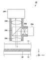
[装置構成について]
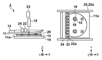
図1は、第1実施形態のインプリント装置1を示す概略図である。インプリント装置1は、モールド11を保持するモールド保持部12と、基板13を保持する基板保持部14と、検出部15と、硬化部21と、観察部23と、撮像部24と、制御部26とを含みうる。また、インプリント装置1は、基板上にインプリント材20を供給する供給部、モールド保持部12を保持するためのブリッジ定盤、基板保持部14を保持するためのベース定盤なども含みうる。
[About device configuration]
FIG. 1 is a schematic view showing the imprinting apparatus 1 of the first embodiment. The imprint device 1 includes a
モールド11は、例えば石英など、インプリント材20を硬化させるための光21a(紫外線)を透過させることが可能な材料で作製されており、基板上のインプリント材20に転写すべきパターン(凹凸パターン)が形成されたパターン領域11aを有する。また、基板13には、例えば単結晶シリコン基板やSOI(Silicon on Insulator)基板などが用いられ、基板13の上面(被処理面)にはインプリント材20が供給(塗布)される。
The
モールド保持部12は、例えば、真空吸着力や静電吸着力などによりモールド11を吸着するモールドチャックと、モールドチャックを載置するモールドステージと、モールドステージを駆動する(移動させる)駆動系とを含みうる。モールド保持部12の駆動系は、モールドステージ(即ち、モールド11)を少なくともZ方向(基板上のインプリント材20にモールド11を押印する際の押印方向)に駆動する。また、モールド保持部12は、硬化部21から射出された、インプリント材20を硬化させる光21aを通過させるための開口12aを有する。ここで、第1実施形態におけるモールド保持部12の駆動系は、Z方向だけではなく、例えばX方向、Y方向およびθ方向(Z軸周りの回転方向)にモールドステージを駆動する機能を備えていてもよい。
The
基板保持部14は、例えば、真空吸着力や静電吸着力などにより基板13を吸着する基板チャックと、基板チャックを載置する基板ステージと、基板ステージを駆動する(移動させる)駆動系とを含みうる。基板保持部14の駆動系は、基板ステージ(即ち、基板13)を少なくともX方向およびY方向(モールド11の押印方向に直交する方向)に駆動する。ここで、第1実施形態における基板保持部14の駆動系は、X方向およびY方向だけではなく、例えばZ方向およびθ方向に基板ステージを駆動する機能を備えていてもよい。
The
検出部15は、モールド11に形成されたマーク18(以下、モールド側のマーク18)と、基板13に形成されたマーク19(以下、基板側のマーク19)とを光学的に検出(観察)するスコープを含む。そして、検出部15は、スコープによる検出結果に基づいて、モールド11と基板13との相対位置を求める。ここで、検出部15は、モールド側のマーク18と基板側のマーク19との相対的な位置関係を検出することができればよい。したがって、検出部15は、2つのマークを同時に撮像するための光学系を備えたスコープを含んでいてもよいし、2つのマークの干渉信号やモアレなどの相対位置関係を反映した信号を検知するスコープを含んでいてもよい。また、検出部15は、モールド側のマーク18と基板側のマーク19とを同時に検出できなくてもよい。例えば、検出部15は、内部に配置された基準位置に対するモールド側のマーク18の位置および基板側のマーク19の位置をそれぞれ求めることで、モールド側のマーク18と基板側のマーク19との相対的な位置関係を検出してもよい。
The
硬化部21は、インプリント材20を硬化させるための光21a(紫外線)を、モールド保持部12の開口12aとモールド11とを介して基板上のインプリント材20に照射し、当該インプリント材20を硬化させる。硬化部21は、例えば、インプリント材20を硬化させるための光21aを射出する光源と、光源から射出された光21aをインプリント処理において最適な光に調整するための光学系とを含みうる。本実施形態のインプリント装置1は、硬化部21から射出された光21aがビームスプリッタ27で反射されて基板13(インプリント材20)に照射されるように構成されうる。
The curing
観察部23は、モールド11のパターン領域11aの全体が収まる視野を有するカメラを含み、光21aの照射による基板上のインプリント材20の硬化状態を観察(確認)する機能を有する。また、観察部23は、モールド11と基板13との間における異物の混入状態、モールド11のパターン領域11aへのインプリント材20の充填状態、基板上の硬化したインプリント材20からのモールド11の離型状態も観察することが可能である。さらに、モールド11と基板上に供給されたインプリント材20との接触状態も観察することが可能である。本実施形態のインプリント装置1は、観察部23がビームスプリッタ27を介してインプリント材20の硬化状態を観察するように構成されている。
The
制御部26は、例えばCPUやメモリなどを含み、インプリント処理を制御する(インプリント装置1の各部を制御する)。本実施形態では、制御部26は、検出部15による検出結果(即ち、モールド11と基板13との相対位置の計測結果)に基づいて、モールド11と基板13とを位置合わせしながらインプリント処理を制御する。また、制御部26は、後述する撮像部24で得られた画像に基づいて、インプリント材20の成形に関する情報を得る。当該情報は、例えば、モールド11と基板13との間への異物の混入に関する情報、モールド11のパターンへのインプリント材20の充填に関する情報、およびモールド11と基板13との重ね合わせに関する情報のうち少なくとも1つを含みうる。
The
モールド保持部12内は限られた空間であるため、各種光学部材や検出部を構成することが難しい場合がある。特に検出部はマーク位置に合わせて駆動する必要があるため、それらの駆動機構を構成するための空間も必要となる。そこで、図11に示すように観察領域の像(マーク18や19の像)を前記構成物の構成しやすい空間に結像させるための光学系(リレー光学系)を構成してもよい。リレー光学系は、複数のリレーレンズ30を備える。
Since the inside of the
リレーレンズ30は、観察領域の像を等倍もしくは拡大、縮小した像としてモールド保持部12外へ結像する。リレーレンズ30は、固定での構成でよいので、レンズなどの光学部材とそれを保持する部材のみの構成でよい。
The
図11に記載のインプリント装置は、検出部15で検出する検出光と、光21aや観察部23用の検出光との合成分離のための光学部材31を設けている。光学部材31は、例えば波長帯域によって反射または透過の性質を持つ光学膜を構成してもよい。図11の構成では、検出部15で使用する波長帯域の光を反射、光21aや観察部23で使用する波長帯域の光を透過する構成で示している。
The imprint device shown in FIG. 11 is provided with an
[モールド側のマークおよび基板側のマークについて]
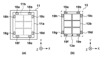
次に、モールド11と基板13との位置合わせに用いられるモールド側のマーク18および基板側のマーク19について、図2を参照しながら説明する。図2では、1回のインプリント処理によってモールド11のパターンが転写されるべき基板上の領域(以下、ショット領域13a)に、6個のチップ領域13aが配置されているものとする。
[About the mark on the mold side and the mark on the substrate side]
Next, the
図2(a)は、モールド11のパターン領域11a、具体的には、パターン領域11aの四隅に設けられたマーク18a〜18hを示す図である。図2(a)において、X方向を長手方向とするマーク18a、18b、18fおよび18eは、X方向を計測方向とするマークであり、Y方向を長手方向とするマーク18c、18d、18gおよび18hは、Y方向を計測方向とするマークである。また、図2(a)には、基板上の6個のチップ領域13bのそれぞれに転写すべきパターンが形成された領域11bが図示されている。
FIG. 2A is a diagram showing marks 18a to 18h provided at the four corners of the
図2(b)は、基板13の1つのショット領域13aに設けられたマーク19a〜19hを示す図である。図2(b)において、X方向を長手方向とするマーク19a、19b、19fおよび19eは、X方向を計測方向とするマークであり、Y方向を長手方向とするマーク19c、19d、19gおよび19hは、Y方向を計測方向とするマークである。また、図2(b)には、6個のチップ領域13bが図示されている。
FIG. 2B is a diagram showing marks 19a to 19h provided in one
モールド11と基板上のインプリント材20とを接触させる際には、モールド側の各マーク18a〜18hとそれに対応する基板側の各マーク19a〜19hとの相対位置が検出部15によって検出される。そして、それぞれの相対位置が目標相対位置になるように、検出部15による検出結果に基づいて、モールド11のパターン領域11aおよび基板13のショット領域13aのうち少なくとも一方の形状や位置が変更される。これにより、モールド11のパターン領域11aと基板13のショット領域13aを精度よく重ね合わせることができる。
When the
[インプリント処理について]
次に、モールド11を用いて基板上のインプリント材20を成形するインプリント処理について、図3を参照しながら説明する。図3は、インプリント処理を説明するための図である。
[About imprint processing]
Next, an imprint process for molding the
まず、図3(a)に示すように、モールド11の押印を開始するまでに、基板上の対象ショット領域(これからインプリント処理を行う対象のショット領域)にインプリント材20を供給する。インプリント装置において一般的に使用されているインプリント材20は揮発性が高いため、インプリント処理を行う直前に基板上にインプリント材20を供給することが好ましい。但し、揮発性が低いインプリント材20を使用する場合では、スピンコータなどによって基板上にインプリント材20を予め供給しておいてもよい。また、インプリント材20を基板上に供給した後、上述したように、モールド側のマーク18と基板側のマーク19との相対位置を検出部15によって検出し、その検出結果に基づいてモールド11と基板13との位置合わせを行う。
First, as shown in FIG. 3A, the
モールド11と基板13との位置合わせを行った後、図3(b)に示すように、モールド11と基板上のインプリント材20とを接触させ、その状態で所定の時間を経過させてモールド11のパターンにインプリント材20を充填させる。このときにおいても、モールド側のマーク18と基板側のマーク19とを検出部15によって検出し、その検出結果に基づいてモールド11と基板13との位置合わせを行うことが好ましい。ここで、モールド11とインプリント材20との屈折率差が小さい場合、モールド側のマーク18が凹凸構造だけで構成されていると、モールド側のマーク18を検出部15で検出することが困難になることがある。したがって、モールド11と異なる屈折率や透過率を有する物質をモールド側のマーク18に塗布したり、イオン照射などによってモールド側のマーク18の屈折率を変えたりするとよい。これにより、モールド11と基板上のインプリント材20とを接触させた状態においても、モールド側のマーク18を検出部15で検出することが可能になる。モールド11のパターンにインプリント材20を充填するための所定の時間が経過したら、硬化部21によって基板上のインプリント材20にモールド11を介して光21aを照射し、当該インプリント材20を硬化させる。
After aligning the
基板上のインプリント材20を硬化させた後、図3(c)に示すように、基板上の硬化したインプリント材20からモールド11を剥離(離型)する。これにより、基板上のインプリント材20にパターンを形成することができる(即ち、基板上にモールド11のパターンを転写することができる)。
After the
[インプリント処理の不具合の検知について]
インプリント装置1では、インプリント処理において、例えば、モールド11と基板13との間に異物が混入したり、モールド11の凹凸パターンへのインプリント材の充填が不十分であったりといった不具合が生じることがある。このような不具合は、次のインプリント処理に引き継がれる可能性があるため、次のインプリント処理の前に検知されることが好ましい。従来のインプリント装置では、基板上のインプリント材20の状態が観察部23によって観察(撮像)され、その観察結果に基づいて当該不具合が検知されていた。ここで、基板上のインプリント材20の状態は、例えば、基板上のインプリント材20の硬化状態、モールド11と基板13との間への異物の混入状態、モールド11のパターンへのインプリント材20の充填状態のうち少なくとも1つを含みうる。また、インプリント材20の状態は、上記に加えて、モールド11と基板上のインプリント材20との接触状態(押印工程)や、硬化したインプリント材20からのモールドの離型状態などを含んでもよい。
[Detection of imprint processing defects]
In the imprint device 1, in the imprint process, for example, foreign matter is mixed between the
インプリント装置では、生産性を向上させるため、1回のインプリント処理においてモールド11のパターンが転写されるショット領域の寸法を大きくすることが好ましい。しかしながら、ショット領域の寸法を大きくすると、モールド11のパターン領域11aの全体が収まる視野を有する観察部23では、十分な解像度でインプリント材20の状態を観察すること(即ち、インプリント材20を撮像すること)が困難になりうる。つまり、従来のインプリント装置では、インプリント処理の不具合を精度よく検知することが困難になりうる。また、モールド11のパターン領域11aの全体が視野に収まる視野を有する観察部23は、パターン領域11aの周辺部において、モールド11に接触している基板上のインプリント材20を斜めから撮像しうる。この場合、モールド11の凹凸パターンにおける複数の凹部に充填されたインプリント材20が重ねて撮像されてしまい、インプリント処理の不具合の検知精度が不十分になりうる。
In the imprint apparatus, in order to improve productivity, it is preferable to increase the size of the shot region to which the pattern of the
そこで、第1実施形態のインプリント装置1は、第1方向(例えばY方向)に沿ってライン状に配列された複数の撮像素子24fを有する撮像部24と、第1方向と異なる第2方向(例えばX方向)に撮像部24を走査させる走査部25とを含む。撮像部24および走査部25は、モールド保持部12の開口12aの内側に設けられうる。そして、制御部26は、インプリント処理において、モールド11とインプリント材20とが接触している状態で、走査部25によって撮像部24を第2方向に走査させながら撮像部24に基板上のインプリント材20を撮像させる。これにより、制御部26は、撮像部24で得られた画像に基づいて、インプリント材20の成形に関する情報を得ることができる。当該情報は、例えば、モールド11と基板13との間への異物の混入に関する情報、モールド11のパターンへのインプリント材20の充填に関する情報、およびモールド11と基板13との重ね合わせ精度に関する情報のうち少なくとも1つを含みうる。撮像部24は、ビームスプリッタ27やリレーレンズ30などの光学部材を介して基板上のインプリント材20を撮像するようにしてもよい。また、基板13の結像面をモールド保持部12の上部に形成し、撮像部24が撮像するようにしてもよい。
Therefore, the imprint device 1 of the first embodiment includes an
[撮像部24の構成について]
次に、撮像部24の構成について、図4を参照しながら説明する。図4は、撮像部24の構成例を示す概略図(X−Z断面図)である。撮像部24は、図4に示すユニットがY方向に複数配列することによって構成され、1つのユニットには、例えば、光源24a、光学部材24b〜24d、ハーフミラー24eおよび撮像素子24f(光電変換素子)が設けられる。光源24aは、インプリント材20を硬化させる光21a(紫外線)とは異なる波長を有する光を射出しうる。光源24aから射出され、光学部材24bを透過した光は、ハーフミラー24eで反射されて、光学部材24cを透過する。そして、モールド11を介してインプリント材20(基板13)で反射された光は、光学部材24c、ハーフミラー24eおよび光学部材24dを透過して、撮像素子24fに入射する。これにより、撮像部24は、インプリント材20(基板13)を撮像することができる。
[About the configuration of the imaging unit 24]
Next, the configuration of the
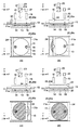
ここで、撮像部24は、撮像領域における長手方向(例えばY方向)の長さがモールド11のパターン領域11aの幅より長くなるように構成されていることが好ましい。このように構成された撮像部24は、走査部25によって第2方向(X方向)に1回だけ走査されることで、モールド11のパターン領域11aが接触したインプリント材20の全体を撮像することができる。しかしながら、それに限られるものではなく、撮像部24は、例えば、図5(a)に示すように、第2方向に1回だけ走査されることで、基板13の全体を撮像することができるように構成されていてもよい。また、撮像部24は、図5(b)に示すように、第2方向に沿って複数回走査されることで、ショット領域の全体(基板13の全体)を撮像することができるように構成されていてもよい。
Here, it is preferable that the
[撮像部24による撮像について]
次に、撮像部24によるインプリント材20(基板13)の撮像について、図6を参照しながら説明する。図6は、撮像部24によるインプリント材20の撮像を説明するための図であり、1回のインプリント処理によってモールド11のパターンを基板13の全体に転写する例を示している。図6(a)〜(d)の各図において、上図がインプリント装置1を横(−Y方向側)から見た図であり、下図がインプリント装置1を上(Z方向側)から見た図である。図6(a)〜(d)の各図では、図をわかり易くするため、制御部26を省略し、モールド保持部12の構成を簡略化している。ここで、撮像部24は、図6に示すように、第2方向(例えばX方向)への走査においてモールド11と検出部15との間を通過するように配置されている。また、走査部25は、例えば、リニアモータなどのアクチュエータを含み、第2方向に伸びるガイドレール25aに沿って撮像部24を走査させる(駆動する)。さらに、インプリント材20を硬化させた後に、検出部15が退避してから撮像部24を走査させて計測してもよい。
[About imaging by the imaging unit 24]
Next, imaging of the imprint material 20 (board 13) by the
まず、制御部26は、図6(a)に示すように、モールド11と基板上のインプリント材20とが接触している状態で、硬化部21によって基板上のインプリント材20にモールド11を介して光を照射し、当該インプリント材20を硬化させる。インプリント材20を硬化させた後、制御部26は、図6(b)および(c)に示すように、走査部25によって撮像部24をX方向に走査させながら、硬化したインプリント材20を撮像部24に撮像させる。図6における斜線部分は、撮像部24によるインプリント材20の撮像が終了した領域を表している。そして、制御部26は、図6(d)に示すように、硬化したインプリント材20を撮像部24によって撮像した後、走査部25による撮像部24の走査を終了させる。このように、撮像部24を走査させながら撮像部24にインプリント材20を撮像させることにより、制御部26は、モールド11(パターン領域11a)が接触し且つ硬化部21によって硬化されたインプリント材20の画像を撮像部24から得ることができる。
First, as shown in FIG. 6A, the
上述したように、第1実施形態のインプリント装置1は、第1方向に配列された複数の撮像素子24fを有する撮像部24を走査部25によって第2方向に走査させながら、モールド11が接触している基板上のインプリント材20を撮像部24に撮像させる。これにより、撮像部24によってインプリント材20を撮像するときの解像度を上げることができるため、撮像部24で得られた画像から、インプリント処理の不具合を精度よく検知することが可能となる。
As described above, in the imprint device 1 of the first embodiment, the
図11のインプリント装置の場合は、リレー光学系(リレーレンズ30)の結像位置に撮像部24を構成することで、同様の効果を得ることができる。
In the case of the imprint device of FIG. 11, the same effect can be obtained by configuring the
前述したように、モールド保持部12内の限られた空間に駆動機構を含めて撮像部24を構成することが困難な場合は、リレーレンズ30でモールド保持部12外へ観察領域の像を結像し、その像を撮像部24で撮像する方がよい。
As described above, when it is difficult to configure the
<第2実施形態>
本発明に係る第2実施形態のインプリント装置2について、図7を参照しながら説明する。図7は、第2実施形態のインプリント装置2を示す概略図である。第2実施形態のインプリント装置2は、第1方向(例えばY方向)に沿ってライン状に配列された複数の光源22aを有する硬化部22を含む。そして、基板上のインプリント材20を硬化させる際、撮像部24の走査方向(第2方向(例えばX方向)に走査部25によって硬化部22を走査させる。このように硬化部22および走査部25を構成することは、基板上のインプリント材20を部分的に硬化させる場合に有利である。
<Second Embodiment>
The imprinting apparatus 2 of the second embodiment according to the present invention will be described with reference to FIG. FIG. 7 is a schematic view showing the imprinting apparatus 2 of the second embodiment. The imprinting apparatus 2 of the second embodiment includes a curing
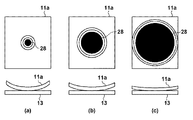
例えば、インプリント装置2では、図8(a)〜(c)に示すように、モールド11と基板上のインプリント材20とを接触させる際に、モールドのパターン領域11aを基板13に向かって突出した凸形状に変形させることがある。モールド11のパターン領域11aを凸形状に変形させると、モールド11とインプリント材20との接触面積をパターン領域11aの中心部から徐々に広げていくことができるため、モールド11のパターンに気泡が残存することを低減することができる。図8(a)〜(c)は、モールド11とインプリント材20との接触面積を徐々に広げていく過程を示す図である。図8(a)〜(c)の各図において、上図はモールド11および基板13を上(Z方向側)から見た図であり、下図はモールド11および基板13を横(−Y方向側)から見た図である。また、黒丸は、モールド11とインプリント材20とが接触した部分(接触部分28)を示している。また、黒い領域の外周にある同心円状のラインは、モールドと基板とによる干渉縞を示している。このようにモールド11とインプリント材20との接触面積を徐々に広げていく場合、その過程で生じるモールド11と基板13との位置ずれを低減するため、当該過程における複数のタイミングの各々でインプリント材20を部分的に硬化させることが好ましい。
For example, in the imprinting apparatus 2, as shown in FIGS. 8A to 8C, when the
また、このように構成されたインプリント装置2では、モールド11とインプリント材20との接触部分28に加えられる押印力(モールド11をインプリント材20に押し付ける力)は、接触面積が徐々に広がるにつれて大きくなる。そのため、例えば、図8(a)に示す接触部分28に異物が混入していると、当該異物によってモールド11や基板13に生じる応力が、接触面積が徐々に広がるにつれて大きくなり、モールド11や基板13が破壊されてしまう虞がある。したがって、接触部分28における不具合(例えば異物)を早い段階で検知することが好ましい。
Further, in the imprinting apparatus 2 configured in this way, the contact area of the imprinting force (force pressing the
そこで、第2実施形態のインプリント装置2は、接触面積を徐々に広げていく過程における複数のタイミングの各々で、走査部25によって硬化部22を走査させながら硬化部22にインプリント材20を硬化させる。それとともに、複数のタイミングの各々で、走査部25によって撮像部24を走査させながら、硬化部22によって硬化されたインプリント材20を撮像部24に撮像させる。ここで、本実施形態における撮像部24は、第1方向(Y方向)に沿ってライン状に配列した複数の撮像素子24fをそれぞれ含む第1撮像部24aおよび第2撮像部24bを有する。第1撮像部24aおよび第2撮像部24bは、第2方向(X方向)において硬化部22を挟み込むように配置されている。このように撮像部24を構成することにより、硬化部22および撮像部24を往復走査させたときであっても、硬化部22によって硬化されたインプリント材20を第1撮像部24aおよび第2撮像部24bのいずれかに撮像させることができる。また、本実施形態における走査部25は、撮像部24の走査および硬化部22の走査においてガイドレール25aを共通に用いる。
Therefore, in the imprint device 2 of the second embodiment, the
第2実施形態のインプリント装置2におけるインプリント材20の撮像について、図9を参照しながら説明する。図9は、撮像部24によるインプリント材20の撮像を説明するための図である。図9(a)〜(c)の各図において、左図がモールド11のパターン領域11aおよび基板13を横(−Y方向側)から見た図であり、右図がモールド11のパターン領域11aおよび基板13を上(Z方向側)から見た図である。また、図9では、右図の斜線部分が、モールド11とインプリント材20との接触部分28に対応する。ここで、第2実施形態のインプリント装置2における検出部15は移動可能に構成されうる。
Imaging of the
まず、制御部26は、接触面積を徐々に広げていく過程における第1タイミングで、モールド11とインプリント材20との接触部分28におけるモールド側のマーク18と基板側のマーク19とを検出部15に検出させる。そして、検出部15による検出結果に基づいてモールド11と基板13との位置合わせを行う。位置合わせを行った後、制御部26は、図9(a)に示すように、走査部25によって硬化部22および撮像部24を+X方向に走査しながら、接触部分28のインプリント材20を硬化部22に硬化させるとともに、第1撮像部24aに基板13を撮像させる。このとき、硬化部22は、複数の光源22aのうち、接触部分28に対応する光源22aのみを用いてインプリント材20を硬化させうる。ここで、制御部26は、走査部25によって硬化部22および撮像部24を走査させる際、硬化部22の走査に追従して撮像部24(第1タイミングでは第1撮像部24a)の走査が行われるように走査部25を制御するとよい。例えば、制御部26は、硬化部22および撮像部24を走査させる際、硬化部22と撮像部24との間隔が一定に保たれるように走査部25を制御するとよい。
First, the
次に、制御部26は、接触面積が更に広がった第2タイミングで、モールド11とインプリント材20との接触部分28におけるモールド側のマーク18と基板側のマーク19とを検出部15に検出させる。そして、検出部15による検出結果に基づいてモールド11と基板13との位置合わせを行う。位置合わせを行った後、制御部26は、図9(b)に示すように、走査部25によって硬化部22および撮像部24を−X方向に走査しながら、接触部分28のインプリント材20を硬化部22に硬化させるとともに、第2撮像部24bに基板13を撮像させる。
Next, the
また、制御部26は、接触面積が更に広がった第3タイミングで、モールド11とインプリント材20との接触部分28におけるモールド側のマーク18と基板側のマーク19とを検出部15に検出させる。そして、検出部15による検出結果に基づいてモールド11と基板13との位置合わせを行う。位置合わせを行った後、制御部26は、図9(c)に示すように、走査部25によって硬化部22および撮像部24を+X方向に走査しながら、接触部分28のインプリント材20を硬化部22に硬化させるとともに、第1撮像部24aに基板13を撮像させる。
Further, the
このようにインプリント処理を行うことにより、第2実施形態のインプリント装置2は、モールド11とインプリント材20との接触面積を徐々に広げていく過程で生じるモールド11と基板13との位置ずれを低減することができる。それとともに、接触部分28における不具合(例えば異物)を早い段階で検知することもできる。
By performing the imprint processing in this way, the imprint device 2 of the second embodiment has a position between the
ここで、第2実施形態では、硬化部22と撮像部24との間隔が一定に保たれるように硬化部22および撮像部24を走査させる例について説明したが、それに限られるものではない。例えば、走査部25によって硬化部を走査させながら接触部分28のインプリント材20を硬化させ、硬化部22の走査が終了した後に撮像部24の走査を開始してもよい。
Here, in the second embodiment, an example in which the
また、第2実施形態では、接触面積を徐々に広げていく過程における複数のタイミングの各々で、硬化部22によるインプリント材20の硬化と、撮像部24によるインプリント材20の撮像とを行ったが、それに限られるものではない。例えば、モールド11とインプリント材20とを接触させる工程が終了した後、即ち、モールド11のパターン領域11aの全体とインプリント材20とが接触した後で、硬化部22による硬化と撮像部24による撮像とを行ってもよい。上記のように、段階的に接触面積を拡げるたびに撮像のみを行い、転写領域が接触しきってから硬化させてもよい。さらに、第2実施形態では、モールド11のパターン領域11aを凸形状に変形させる例について説明したが、基板13をモールド11に向かった凸形状に変形させてもよい。
Further, in the second embodiment, the
<第3実施形態>
第2実施形態では、パターン領域11aの中央部からモールド11とインプリント材20とを徐々に接触させる例について説明したが、それに限られるものではない。例えば、図10に示すように、パターン領域11aの端部からモールド11とインプリント材20とを接触させる場合においても本発明を適用することができる。図10は、パターン領域11aの端部からモールド11とインプリント材20を接触させる場合における撮像部24によるインプリント材20の撮像を説明するための図である。図10において、左図はインプリント装置2を横(−Y方向側)から見た図であり、右図はインプリント装置2を上(Z方向側)から見た図である。
<Third Embodiment>
In the second embodiment, an example in which the
パターン領域11aの端部からモールド11とインプリント材20とを接触させていくと、接触部分と非接触部分との境界(以下、単に「境界」と称する)が移動する。制御部26は、モールド11とインプリント材20との接触面積の拡がり(即ち、境界の移動)に追従するように検出部15を移動させ、当該接触部分におけるモールド側のマーク18と基板側のマーク19とを検出部15に順次検出させる。そして、制御部26は、検出部15による検出結果に基づいてモールド11と基板13との位置合わせを行う。また、制御部26は、接触面積の拡がり(境界の移動)に追従するように、走査部25によって硬化部22および撮像部24を走査しながら、位置合わせが行われた接触部分のインプリント材20を硬化部22に順次硬化させる。それとともに、硬化部22によって硬化されたインプリント材20を撮像部24に順次撮像させる。
When the
上述の実施形態では、基板13の全面を一度にパターン形成する構成を主として述べたがこれにこだわらない。
In the above-described embodiment, the configuration in which the entire surface of the
図12は、一回のインプリント処理によって基板13上にパターンが形成される領域を説明するための図である。図12に示したA領域は、1つのショット領域を示している。1つのショット領域は、例えばインプリント装置とは異なるリソグラフィ装置でパターンが形成された領域を示す。生産性を上げるため、複数のショット領域に対して同時にインプリント処理を行う手法が提案されている。例として、図12では、2つのショット領域に対して同時にインプリント処理を行うB領域や、4つのショット領域に対して同時にインプリント処理を行うC領域が示されている。
FIG. 12 is a diagram for explaining a region where a pattern is formed on the
観察部23は、同時にインプリント処理を行う領域が増えるほど、観察すべき範囲が増えるため、画像分解能が低下していく。したがって、基板全面に対して一度にインプリント処理を行う形態でなくとも、複数のショット領域に対して同時にインプリント処理を行う形態においても同様の効果を得ることができる。
As the area to be imprinted by the
<物品の製造方法の実施形態>
本発明の実施形態にかかる物品の製造方法は、例えば、半導体デバイス等のマイクロデバイスや微細構造を有する素子等の物品を製造するのに好適である。本実施形態の物品の製造方法は、基板上に供給されたインプリント材に上記のインプリント装置を用いてパターンを形成する工程と、かかる工程でパターンを形成された基板を加工する工程とを含む。更に、かかる製造方法は、他の周知の工程(酸化、成膜、蒸着、ドーピング、平坦化、エッチング、レジスト剥離、ダイシング、ボンディング、パッケージング等)を含む。本実施形態の物品の製造方法は、従来の方法に比べて、物品の性能・品質・生産性・生産コストの少なくとも1つにおいて有利である。
<Embodiment of manufacturing method of article>
The method for manufacturing an article according to the embodiment of the present invention is suitable for producing an article such as a microdevice such as a semiconductor device or an element having a fine structure. The method for manufacturing an article of the present embodiment includes a step of forming a pattern on the imprint material supplied on the substrate by using the above-mentioned imprint device and a step of processing the substrate on which the pattern is formed in such a step. Including. Further, such a manufacturing method includes other well-known steps (oxidation, film formation, vapor deposition, doping, flattening, etching, resist peeling, dicing, bonding, packaging, etc.). The method for producing an article of the present embodiment is advantageous in at least one of the performance, quality, productivity, and production cost of the article as compared with the conventional method.
以上、本発明の好ましい実施形態について説明したが、本発明はこれらの実施形態に限定されないことはいうまでもなく、その要旨の範囲内で種々の変形および変更が可能である。 Although the preferred embodiments of the present invention have been described above, it goes without saying that the present invention is not limited to these embodiments, and various modifications and modifications can be made within the scope of the gist thereof.
1,2:インプリント装置、11:モールド、12:モールド保持部、13:基板、14:基板保持部、15:検出部、21,22:硬化部、23:観察部、24:撮像部、25:走査部、26:制御部 1,2: Imprint device, 11: Mold, 12: Mold holding part, 13: Substrate, 14: Board holding part, 15: Detection part, 21,22: Curing part, 23: Observation part, 24: Imaging part, 25: Scanning unit, 26: Control unit
Claims (15)
前記インプリント材を撮像する撮像部と、
前記モールドと前記インプリント材とが接触している状態で、前記撮像部を走査させながら前記撮像部に前記インプリント材を撮像させ、前記撮像部で得られた画像に基づいて前記インプリント材の成形に関する情報を得る制御部と、
を含むことを特徴とするインプリント装置。 An imprinting device that molds an imprint material on a substrate using a mold.
An imaging unit that captures the imprint material and
In a state where the mold and the imprint material are in contact with each other, the imprint material is imaged by the image pickup unit while scanning the image pickup unit, and the imprint material is based on the image obtained by the image pickup unit. Control unit that obtains information about molding of
An imprinting device characterized by including.
前記制御部は、前記長手方向と異なる方向に前記撮像部を走査させながら、前記パターン領域が接触している前記インプリント材を前記撮像部に撮像させ、前記撮像部で得られた画像に基づいて前記情報を得る、ことを特徴とする請求項1乃至3のうちいずれか1項に記載のインプリント装置。 The length of the imaging unit in the imaging region in the longitudinal direction is longer than the width of the pattern region of the mold.
The control unit scans the image pickup unit in a direction different from the longitudinal direction, causes the image pickup unit to image the imprint material in contact with the pattern region, and is based on the image obtained by the image pickup unit. The imprinting apparatus according to any one of claims 1 to 3, wherein the information is obtained.
前記撮像部は、前記開口の内側に配置されている、ことを特徴とする請求項1乃至4のうちいずれか1項に記載のインプリント装置。 Further comprising a mold holding portion having an opening for holding the mold and allowing light to pass through to cure the imprint material.
The imprinting apparatus according to any one of claims 1 to 4, wherein the imaging unit is arranged inside the opening.
前記制御部は、前記モールドが接触しており且つ前記硬化部によって硬化された前記インプリント材を、前記撮像部を走査させながら前記撮像部に撮像させ、前記撮像部で得られた画像に基づいて前記情報を得る、ことを特徴とする請求項1乃至5のうちいずれか1項に記載のインプリント装置。 The imprint material is further irradiated with light to further include a cured portion that cures the imprint material.
The control unit causes the imaging unit to take an image of the imprint material that the mold is in contact with and is cured by the curing unit while scanning the imaging unit, and based on the image obtained by the imaging unit. The imprinting apparatus according to any one of claims 1 to 5, wherein the information is obtained.
前記撮像部は、前記モールドに対する走査において前記モールドと前記検出部との間を通過するように配置されている、ことを特徴とする請求項1乃至11のうちいずれか1項に記載のインプリント装置。 Further including a detection unit for detecting a mark provided on the mold and a mark provided on the substrate.
The imprint according to any one of claims 1 to 11, wherein the imaging unit is arranged so as to pass between the mold and the detection unit in scanning with respect to the mold. apparatus.
前記工程でパターンを形成された前記基板を加工する工程と、
を含むことを特徴とする物品の製造方法。 A step of forming a pattern on a substrate by using the imprinting apparatus according to any one of claims 1 to 14.
The process of processing the substrate on which the pattern was formed in the process and
A method of manufacturing an article, which comprises.
Priority Applications (5)
| Application Number | Priority Date | Filing Date | Title |
|---|---|---|---|
| JP2016132779A JP6799397B2 (en) | 2015-08-10 | 2016-07-04 | Imprinting equipment and manufacturing method of articles |
| US15/224,911 US10011057B2 (en) | 2015-08-10 | 2016-08-01 | Imprint apparatus, and method of manufacturing article |
| KR1020197002514A KR102241655B1 (en) | 2015-08-10 | 2017-01-26 | Imprint device and article manufacturing method |
| PCT/JP2017/002625 WO2018008174A1 (en) | 2015-08-10 | 2017-01-26 | Imprint device and method for manufacturing article |
| TW106103720A TWI737675B (en) | 2015-08-10 | 2017-02-03 | Imprint apparatus, and method of manufacturing article |
Applications Claiming Priority (3)
| Application Number | Priority Date | Filing Date | Title |
|---|---|---|---|
| JP2015158495 | 2015-08-10 | ||
| JP2015158495 | 2015-08-10 | ||
| JP2016132779A JP6799397B2 (en) | 2015-08-10 | 2016-07-04 | Imprinting equipment and manufacturing method of articles |
Publications (3)
| Publication Number | Publication Date |
|---|---|
| JP2017038042A JP2017038042A (en) | 2017-02-16 |
| JP2017038042A5 JP2017038042A5 (en) | 2019-07-25 |
| JP6799397B2 true JP6799397B2 (en) | 2020-12-16 |
Family
ID=57994655
Family Applications (1)
| Application Number | Title | Priority Date | Filing Date |
|---|---|---|---|
| JP2016132779A Active JP6799397B2 (en) | 2015-08-10 | 2016-07-04 | Imprinting equipment and manufacturing method of articles |
Country Status (5)
| Country | Link |
|---|---|
| US (1) | US10011057B2 (en) |
| JP (1) | JP6799397B2 (en) |
| KR (1) | KR102241655B1 (en) |
| TW (1) | TWI737675B (en) |
| WO (1) | WO2018008174A1 (en) |
Families Citing this family (9)
| Publication number | Priority date | Publication date | Assignee | Title |
|---|---|---|---|---|
| JP6188382B2 (en) * | 2013-04-03 | 2017-08-30 | キヤノン株式会社 | Imprint apparatus and article manufacturing method |
| JP5960198B2 (en) * | 2013-07-02 | 2016-08-02 | キヤノン株式会社 | Pattern forming method, lithographic apparatus, lithographic system, and article manufacturing method |
| US10353299B2 (en) * | 2016-06-01 | 2019-07-16 | Canon Kabushiki Kaisha | Lithography method, determination method, information processing apparatus, storage medium, and method of manufacturing article |
| JP7222623B2 (en) * | 2018-07-23 | 2023-02-15 | キヤノン株式会社 | Pattern forming method and article manufacturing method |
| US11107678B2 (en) | 2019-11-26 | 2021-08-31 | Canon Kabushiki Kaisha | Wafer process, apparatus and method of manufacturing an article |
| KR102227885B1 (en) * | 2020-06-02 | 2021-03-15 | 주식회사 기가레인 | Transfer apparatus capable of pattern alignment |
| JP7494037B2 (en) * | 2020-07-15 | 2024-06-03 | キヤノン株式会社 | Information processing device, judgment method, inspection device, molding device, and article manufacturing method |
| KR102520642B1 (en) * | 2020-12-29 | 2023-04-11 | 주식회사 기가레인 | Transfer apparatus capable of pattern alignment |
| JP7407465B2 (en) * | 2022-03-04 | 2024-01-04 | 株式会社菊水製作所 | Molded product processing system |
Family Cites Families (17)
| Publication number | Priority date | Publication date | Assignee | Title |
|---|---|---|---|---|
| GB2432029A (en) * | 2005-11-02 | 2007-05-09 | Crime Scene Invest Equipment L | Imprint identification system using image scanner calibration |
| US7854867B2 (en) * | 2006-04-21 | 2010-12-21 | Molecular Imprints, Inc. | Method for detecting a particle in a nanoimprint lithography system |
| US7815824B2 (en) * | 2008-02-26 | 2010-10-19 | Molecular Imprints, Inc. | Real time imprint process diagnostics for defects |
| US8345242B2 (en) * | 2008-10-28 | 2013-01-01 | Molecular Imprints, Inc. | Optical system for use in stage control |
| JP5173944B2 (en) | 2009-06-16 | 2013-04-03 | キヤノン株式会社 | Imprint apparatus and article manufacturing method |
| JP5455583B2 (en) | 2009-11-30 | 2014-03-26 | キヤノン株式会社 | Imprint device |
| JP5539011B2 (en) * | 2010-05-14 | 2014-07-02 | キヤノン株式会社 | Imprint apparatus, detection apparatus, alignment apparatus, and article manufacturing method |
| JP5597031B2 (en) * | 2010-05-31 | 2014-10-01 | キヤノン株式会社 | Lithographic apparatus and article manufacturing method |
| JP5576822B2 (en) * | 2011-03-25 | 2014-08-20 | 富士フイルム株式会社 | Method for removing foreign matter adhering to the mold |
| JP6039222B2 (en) * | 2011-05-10 | 2016-12-07 | キヤノン株式会社 | Detection apparatus, detection method, imprint apparatus, and device manufacturing method |
| JP6071221B2 (en) * | 2012-03-14 | 2017-02-01 | キヤノン株式会社 | Imprint apparatus, mold, imprint method, and article manufacturing method |
| JP6140990B2 (en) * | 2012-11-30 | 2017-06-07 | キヤノン株式会社 | Measuring apparatus, imprint system, measuring method, and device manufacturing method |
| JP6119474B2 (en) * | 2013-07-12 | 2017-04-26 | 大日本印刷株式会社 | Imprint apparatus and imprint method |
| JP6083340B2 (en) * | 2013-07-12 | 2017-02-22 | 富士通株式会社 | Compound semiconductor device and manufacturing method thereof |
| JP6282069B2 (en) | 2013-09-13 | 2018-02-21 | キヤノン株式会社 | Imprint apparatus, imprint method, detection method, and device manufacturing method |
| JP6415120B2 (en) | 2014-06-09 | 2018-10-31 | キヤノン株式会社 | Imprint apparatus and article manufacturing method |
| JP6403627B2 (en) * | 2015-04-14 | 2018-10-10 | キヤノン株式会社 | Imprint apparatus, imprint method, and article manufacturing method |
-
2016
- 2016-07-04 JP JP2016132779A patent/JP6799397B2/en active Active
- 2016-08-01 US US15/224,911 patent/US10011057B2/en active Active
-
2017
- 2017-01-26 KR KR1020197002514A patent/KR102241655B1/en active Active
- 2017-01-26 WO PCT/JP2017/002625 patent/WO2018008174A1/en not_active Ceased
- 2017-02-03 TW TW106103720A patent/TWI737675B/en active
Also Published As
| Publication number | Publication date |
|---|---|
| TW201802873A (en) | 2018-01-16 |
| KR20190022763A (en) | 2019-03-06 |
| KR102241655B1 (en) | 2021-04-19 |
| JP2017038042A (en) | 2017-02-16 |
| TWI737675B (en) | 2021-09-01 |
| US20170043511A1 (en) | 2017-02-16 |
| WO2018008174A1 (en) | 2018-01-11 |
| US10011057B2 (en) | 2018-07-03 |
Similar Documents
| Publication | Publication Date | Title |
|---|---|---|
| JP6799397B2 (en) | Imprinting equipment and manufacturing method of articles | |
| JP6360287B2 (en) | Lithographic apparatus, alignment method, and article manufacturing method | |
| US9442370B2 (en) | Imprinting method, imprinting apparatus, and device manufacturing method | |
| KR101597387B1 (en) | Detector, imprint apparatus, and article manufacturing method | |
| TWI625761B (en) | Imprinting apparatus and method of manufacturing the same | |
| JP2015029070A (en) | Pattern formation method, lithography device, lithography system, and article manufacturing method | |
| KR101573572B1 (en) | Imprint apparatus, article manufacturing method and pattern transfer method | |
| KR20200055079A (en) | Imprint apparatus and manufacturing method of articles | |
| CN104614937A (en) | Imprint apparatus | |
| CN105759566A (en) | Imprint Apparatus, Imprint Method, And Method Of Manufacturing Article | |
| KR102867554B1 (en) | Imprinting method, pre-processing apparatus, substrate for imprinting, and method for manufacturing substrate | |
| JP2019062164A (en) | Imprint device, imprint method, determination method of arrangement pattern of imprint material, and manufacturing method of article | |
| JP6792669B2 (en) | Pattern formation method, lithography equipment, lithography system and article manufacturing method | |
| TW202040645A (en) | Measuring device, pattern forming device and manufacturing method of article | |
| JP2018010927A (en) | Imprint apparatus, imprint method, and article manufacturing method | |
| JP6209903B2 (en) | INSPECTION METHOD, NANOIMPRINT MOLD MANUFACTURING METHOD, NANOIMPRINT METHOD, AND INSPECTION DEVICE |
Legal Events
| Date | Code | Title | Description |
|---|---|---|---|
| A521 | Request for written amendment filed |
Free format text: JAPANESE INTERMEDIATE CODE: A523 Effective date: 20190619 |
|
| A621 | Written request for application examination |
Free format text: JAPANESE INTERMEDIATE CODE: A621 Effective date: 20190619 |
|
| A131 | Notification of reasons for refusal |
Free format text: JAPANESE INTERMEDIATE CODE: A131 Effective date: 20200413 |
|
| A521 | Request for written amendment filed |
Free format text: JAPANESE INTERMEDIATE CODE: A523 Effective date: 20200605 |
|
| TRDD | Decision of grant or rejection written | ||
| A01 | Written decision to grant a patent or to grant a registration (utility model) |
Free format text: JAPANESE INTERMEDIATE CODE: A01 Effective date: 20201023 |
|
| A61 | First payment of annual fees (during grant procedure) |
Free format text: JAPANESE INTERMEDIATE CODE: A61 Effective date: 20201120 |
|
| R151 | Written notification of patent or utility model registration |
Ref document number: 6799397 Country of ref document: JP Free format text: JAPANESE INTERMEDIATE CODE: R151 |