JP6798293B2 - Method for manufacturing silicon carbide epitaxial substrate and silicon carbide semiconductor device - Google Patents
Method for manufacturing silicon carbide epitaxial substrate and silicon carbide semiconductor device Download PDFInfo
- Publication number
- JP6798293B2 JP6798293B2 JP2016238507A JP2016238507A JP6798293B2 JP 6798293 B2 JP6798293 B2 JP 6798293B2 JP 2016238507 A JP2016238507 A JP 2016238507A JP 2016238507 A JP2016238507 A JP 2016238507A JP 6798293 B2 JP6798293 B2 JP 6798293B2
- Authority
- JP
- Japan
- Prior art keywords
- silicon carbide
- main surface
- dislocation
- epitaxial substrate
- single crystal
- Prior art date
- Legal status (The legal status is an assumption and is not a legal conclusion. Google has not performed a legal analysis and makes no representation as to the accuracy of the status listed.)
- Active
Links
- 229910010271 silicon carbide Inorganic materials 0.000 title claims description 227
- HBMJWWWQQXIZIP-UHFFFAOYSA-N silicon carbide Chemical compound [Si+]#[C-] HBMJWWWQQXIZIP-UHFFFAOYSA-N 0.000 title claims description 225
- 239000000758 substrate Substances 0.000 title claims description 140
- 238000004519 manufacturing process Methods 0.000 title claims description 31
- 238000000034 method Methods 0.000 title claims description 27
- 239000004065 semiconductor Substances 0.000 title claims description 23
- 239000013078 crystal Substances 0.000 claims description 68
- 230000002093 peripheral effect Effects 0.000 claims description 16
- 238000003491 array Methods 0.000 claims description 2
- 239000010410 layer Substances 0.000 description 79
- 239000007789 gas Substances 0.000 description 41
- 238000006243 chemical reaction Methods 0.000 description 29
- 238000001816 cooling Methods 0.000 description 22
- 238000010438 heat treatment Methods 0.000 description 16
- KWYUFKZDYYNOTN-UHFFFAOYSA-M Potassium hydroxide Chemical compound [OH-].[K+] KWYUFKZDYYNOTN-UHFFFAOYSA-M 0.000 description 12
- QGZKDVFQNNGYKY-UHFFFAOYSA-N Ammonia Chemical compound N QGZKDVFQNNGYKY-UHFFFAOYSA-N 0.000 description 11
- 239000002994 raw material Substances 0.000 description 10
- 239000012159 carrier gas Substances 0.000 description 9
- 239000012535 impurity Substances 0.000 description 9
- 230000015572 biosynthetic process Effects 0.000 description 8
- 230000007246 mechanism Effects 0.000 description 8
- 230000008569 process Effects 0.000 description 8
- IJGRMHOSHXDMSA-UHFFFAOYSA-N Atomic nitrogen Chemical compound N#N IJGRMHOSHXDMSA-UHFFFAOYSA-N 0.000 description 7
- 230000007423 decrease Effects 0.000 description 7
- VYPSYNLAJGMNEJ-UHFFFAOYSA-N silicon dioxide Inorganic materials O=[Si]=O VYPSYNLAJGMNEJ-UHFFFAOYSA-N 0.000 description 7
- 239000011229 interlayer Substances 0.000 description 6
- 238000005468 ion implantation Methods 0.000 description 6
- 230000004913 activation Effects 0.000 description 5
- 238000000137 annealing Methods 0.000 description 5
- 210000000746 body region Anatomy 0.000 description 5
- 235000012239 silicon dioxide Nutrition 0.000 description 5
- MWUXSHHQAYIFBG-UHFFFAOYSA-N Nitric oxide Chemical compound O=[N] MWUXSHHQAYIFBG-UHFFFAOYSA-N 0.000 description 4
- ATUOYWHBWRKTHZ-UHFFFAOYSA-N Propane Chemical compound CCC ATUOYWHBWRKTHZ-UHFFFAOYSA-N 0.000 description 4
- 229910052782 aluminium Inorganic materials 0.000 description 4
- XAGFODPZIPBFFR-UHFFFAOYSA-N aluminium Chemical compound [Al] XAGFODPZIPBFFR-UHFFFAOYSA-N 0.000 description 4
- 239000012298 atmosphere Substances 0.000 description 4
- 238000005229 chemical vapour deposition Methods 0.000 description 4
- 238000005530 etching Methods 0.000 description 4
- 230000006698 induction Effects 0.000 description 4
- BLRPTPMANUNPDV-UHFFFAOYSA-N Silane Chemical compound [SiH4] BLRPTPMANUNPDV-UHFFFAOYSA-N 0.000 description 3
- 239000002019 doping agent Substances 0.000 description 3
- 229910052757 nitrogen Inorganic materials 0.000 description 3
- 238000002360 preparation method Methods 0.000 description 3
- 239000010453 quartz Substances 0.000 description 3
- 229910000077 silane Inorganic materials 0.000 description 3
- XKRFYHLGVUSROY-UHFFFAOYSA-N Argon Chemical compound [Ar] XKRFYHLGVUSROY-UHFFFAOYSA-N 0.000 description 2
- UFHFLCQGNIYNRP-UHFFFAOYSA-N Hydrogen Chemical compound [H][H] UFHFLCQGNIYNRP-UHFFFAOYSA-N 0.000 description 2
- PXHVJJICTQNCMI-UHFFFAOYSA-N Nickel Chemical compound [Ni] PXHVJJICTQNCMI-UHFFFAOYSA-N 0.000 description 2
- GQPLMRYTRLFLPF-UHFFFAOYSA-N Nitrous Oxide Chemical compound [O-][N+]#N GQPLMRYTRLFLPF-UHFFFAOYSA-N 0.000 description 2
- XUIMIQQOPSSXEZ-UHFFFAOYSA-N Silicon Chemical compound [Si] XUIMIQQOPSSXEZ-UHFFFAOYSA-N 0.000 description 2
- 239000012300 argon atmosphere Substances 0.000 description 2
- 238000010586 diagram Methods 0.000 description 2
- 239000001257 hydrogen Substances 0.000 description 2
- 229910052739 hydrogen Inorganic materials 0.000 description 2
- 230000003647 oxidation Effects 0.000 description 2
- 238000007254 oxidation reaction Methods 0.000 description 2
- 239000001294 propane Substances 0.000 description 2
- 230000009467 reduction Effects 0.000 description 2
- 229910052710 silicon Inorganic materials 0.000 description 2
- 239000010703 silicon Substances 0.000 description 2
- 239000000377 silicon dioxide Substances 0.000 description 2
- OKTJSMMVPCPJKN-UHFFFAOYSA-N Carbon Chemical compound [C] OKTJSMMVPCPJKN-UHFFFAOYSA-N 0.000 description 1
- 229910005883 NiSi Inorganic materials 0.000 description 1
- OAICVXFJPJFONN-UHFFFAOYSA-N Phosphorus Chemical compound [P] OAICVXFJPJFONN-UHFFFAOYSA-N 0.000 description 1
- 229910004298 SiO 2 Inorganic materials 0.000 description 1
- RTAQQCXQSZGOHL-UHFFFAOYSA-N Titanium Chemical compound [Ti] RTAQQCXQSZGOHL-UHFFFAOYSA-N 0.000 description 1
- 229910045601 alloy Inorganic materials 0.000 description 1
- 239000000956 alloy Substances 0.000 description 1
- 229910021529 ammonia Inorganic materials 0.000 description 1
- 229910052786 argon Inorganic materials 0.000 description 1
- QVGXLLKOCUKJST-UHFFFAOYSA-N atomic oxygen Chemical compound [O] QVGXLLKOCUKJST-UHFFFAOYSA-N 0.000 description 1
- 230000004888 barrier function Effects 0.000 description 1
- 239000000969 carrier Substances 0.000 description 1
- 230000015556 catabolic process Effects 0.000 description 1
- 238000000354 decomposition reaction Methods 0.000 description 1
- 229910001873 dinitrogen Inorganic materials 0.000 description 1
- 238000009826 distribution Methods 0.000 description 1
- 230000000694 effects Effects 0.000 description 1
- 230000005684 electric field Effects 0.000 description 1
- 230000005669 field effect Effects 0.000 description 1
- -1 for example Substances 0.000 description 1
- 229910002804 graphite Inorganic materials 0.000 description 1
- 239000010439 graphite Substances 0.000 description 1
- 150000002431 hydrogen Chemical class 0.000 description 1
- 230000006872 improvement Effects 0.000 description 1
- 239000011810 insulating material Substances 0.000 description 1
- 239000012774 insulation material Substances 0.000 description 1
- 239000000463 material Substances 0.000 description 1
- 229910044991 metal oxide Inorganic materials 0.000 description 1
- 150000004706 metal oxides Chemical class 0.000 description 1
- 230000004048 modification Effects 0.000 description 1
- 238000012986 modification Methods 0.000 description 1
- 229910052759 nickel Inorganic materials 0.000 description 1
- 239000012299 nitrogen atmosphere Substances 0.000 description 1
- 239000001272 nitrous oxide Substances 0.000 description 1
- 230000003287 optical effect Effects 0.000 description 1
- 239000001301 oxygen Substances 0.000 description 1
- 229910052760 oxygen Inorganic materials 0.000 description 1
- 229910052698 phosphorus Inorganic materials 0.000 description 1
- 239000011574 phosphorus Substances 0.000 description 1
- 229910021420 polycrystalline silicon Inorganic materials 0.000 description 1
- 229920005591 polysilicon Polymers 0.000 description 1
- 230000002040 relaxant effect Effects 0.000 description 1
- 238000004544 sputter deposition Methods 0.000 description 1
- 238000005092 sublimation method Methods 0.000 description 1
- 239000010936 titanium Substances 0.000 description 1
- 229910052719 titanium Inorganic materials 0.000 description 1
- 238000011144 upstream manufacturing Methods 0.000 description 1
Images


Classifications
-
- C—CHEMISTRY; METALLURGY
- C30—CRYSTAL GROWTH
- C30B—SINGLE-CRYSTAL GROWTH; UNIDIRECTIONAL SOLIDIFICATION OF EUTECTIC MATERIAL OR UNIDIRECTIONAL DEMIXING OF EUTECTOID MATERIAL; REFINING BY ZONE-MELTING OF MATERIAL; PRODUCTION OF A HOMOGENEOUS POLYCRYSTALLINE MATERIAL WITH DEFINED STRUCTURE; SINGLE CRYSTALS OR HOMOGENEOUS POLYCRYSTALLINE MATERIAL WITH DEFINED STRUCTURE; AFTER-TREATMENT OF SINGLE CRYSTALS OR A HOMOGENEOUS POLYCRYSTALLINE MATERIAL WITH DEFINED STRUCTURE; APPARATUS THEREFOR
- C30B29/00—Single crystals or homogeneous polycrystalline material with defined structure characterised by the material or by their shape
- C30B29/10—Inorganic compounds or compositions
- C30B29/36—Carbides
-
- C—CHEMISTRY; METALLURGY
- C30—CRYSTAL GROWTH
- C30B—SINGLE-CRYSTAL GROWTH; UNIDIRECTIONAL SOLIDIFICATION OF EUTECTIC MATERIAL OR UNIDIRECTIONAL DEMIXING OF EUTECTOID MATERIAL; REFINING BY ZONE-MELTING OF MATERIAL; PRODUCTION OF A HOMOGENEOUS POLYCRYSTALLINE MATERIAL WITH DEFINED STRUCTURE; SINGLE CRYSTALS OR HOMOGENEOUS POLYCRYSTALLINE MATERIAL WITH DEFINED STRUCTURE; AFTER-TREATMENT OF SINGLE CRYSTALS OR A HOMOGENEOUS POLYCRYSTALLINE MATERIAL WITH DEFINED STRUCTURE; APPARATUS THEREFOR
- C30B25/00—Single-crystal growth by chemical reaction of reactive gases, e.g. chemical vapour-deposition growth
- C30B25/02—Epitaxial-layer growth
- C30B25/18—Epitaxial-layer growth characterised by the substrate
- C30B25/186—Epitaxial-layer growth characterised by the substrate being specially pre-treated by, e.g. chemical or physical means
-
- C—CHEMISTRY; METALLURGY
- C30—CRYSTAL GROWTH
- C30B—SINGLE-CRYSTAL GROWTH; UNIDIRECTIONAL SOLIDIFICATION OF EUTECTIC MATERIAL OR UNIDIRECTIONAL DEMIXING OF EUTECTOID MATERIAL; REFINING BY ZONE-MELTING OF MATERIAL; PRODUCTION OF A HOMOGENEOUS POLYCRYSTALLINE MATERIAL WITH DEFINED STRUCTURE; SINGLE CRYSTALS OR HOMOGENEOUS POLYCRYSTALLINE MATERIAL WITH DEFINED STRUCTURE; AFTER-TREATMENT OF SINGLE CRYSTALS OR A HOMOGENEOUS POLYCRYSTALLINE MATERIAL WITH DEFINED STRUCTURE; APPARATUS THEREFOR
- C30B25/00—Single-crystal growth by chemical reaction of reactive gases, e.g. chemical vapour-deposition growth
- C30B25/02—Epitaxial-layer growth
- C30B25/18—Epitaxial-layer growth characterised by the substrate
- C30B25/20—Epitaxial-layer growth characterised by the substrate the substrate being of the same materials as the epitaxial layer
-
- H—ELECTRICITY
- H01—ELECTRIC ELEMENTS
- H01L—SEMICONDUCTOR DEVICES NOT COVERED BY CLASS H10
- H01L21/00—Processes or apparatus adapted for the manufacture or treatment of semiconductor or solid state devices or of parts thereof
- H01L21/02—Manufacture or treatment of semiconductor devices or of parts thereof
- H01L21/02104—Forming layers
- H01L21/02365—Forming inorganic semiconducting materials on a substrate
- H01L21/02367—Substrates
- H01L21/0237—Materials
- H01L21/02373—Group 14 semiconducting materials
- H01L21/02378—Silicon carbide
-
- H—ELECTRICITY
- H01—ELECTRIC ELEMENTS
- H01L—SEMICONDUCTOR DEVICES NOT COVERED BY CLASS H10
- H01L21/00—Processes or apparatus adapted for the manufacture or treatment of semiconductor or solid state devices or of parts thereof
- H01L21/02—Manufacture or treatment of semiconductor devices or of parts thereof
- H01L21/02104—Forming layers
- H01L21/02365—Forming inorganic semiconducting materials on a substrate
- H01L21/02367—Substrates
- H01L21/02428—Structure
- H01L21/0243—Surface structure
-
- H—ELECTRICITY
- H01—ELECTRIC ELEMENTS
- H01L—SEMICONDUCTOR DEVICES NOT COVERED BY CLASS H10
- H01L21/00—Processes or apparatus adapted for the manufacture or treatment of semiconductor or solid state devices or of parts thereof
- H01L21/02—Manufacture or treatment of semiconductor devices or of parts thereof
- H01L21/02104—Forming layers
- H01L21/02365—Forming inorganic semiconducting materials on a substrate
- H01L21/02367—Substrates
- H01L21/02433—Crystal orientation
-
- H—ELECTRICITY
- H01—ELECTRIC ELEMENTS
- H01L—SEMICONDUCTOR DEVICES NOT COVERED BY CLASS H10
- H01L21/00—Processes or apparatus adapted for the manufacture or treatment of semiconductor or solid state devices or of parts thereof
- H01L21/02—Manufacture or treatment of semiconductor devices or of parts thereof
- H01L21/02104—Forming layers
- H01L21/02365—Forming inorganic semiconducting materials on a substrate
- H01L21/02518—Deposited layers
- H01L21/02521—Materials
- H01L21/02524—Group 14 semiconducting materials
- H01L21/02529—Silicon carbide
-
- H—ELECTRICITY
- H01—ELECTRIC ELEMENTS
- H01L—SEMICONDUCTOR DEVICES NOT COVERED BY CLASS H10
- H01L21/00—Processes or apparatus adapted for the manufacture or treatment of semiconductor or solid state devices or of parts thereof
- H01L21/02—Manufacture or treatment of semiconductor devices or of parts thereof
- H01L21/02104—Forming layers
- H01L21/02365—Forming inorganic semiconducting materials on a substrate
- H01L21/02518—Deposited layers
- H01L21/0257—Doping during depositing
- H01L21/02573—Conductivity type
- H01L21/02576—N-type
-
- H—ELECTRICITY
- H01—ELECTRIC ELEMENTS
- H01L—SEMICONDUCTOR DEVICES NOT COVERED BY CLASS H10
- H01L21/00—Processes or apparatus adapted for the manufacture or treatment of semiconductor or solid state devices or of parts thereof
- H01L21/02—Manufacture or treatment of semiconductor devices or of parts thereof
- H01L21/02104—Forming layers
- H01L21/02365—Forming inorganic semiconducting materials on a substrate
- H01L21/02518—Deposited layers
- H01L21/02609—Crystal orientation
-
- H—ELECTRICITY
- H01—ELECTRIC ELEMENTS
- H01L—SEMICONDUCTOR DEVICES NOT COVERED BY CLASS H10
- H01L21/00—Processes or apparatus adapted for the manufacture or treatment of semiconductor or solid state devices or of parts thereof
- H01L21/02—Manufacture or treatment of semiconductor devices or of parts thereof
- H01L21/02104—Forming layers
- H01L21/02365—Forming inorganic semiconducting materials on a substrate
- H01L21/02612—Formation types
- H01L21/02617—Deposition types
- H01L21/0262—Reduction or decomposition of gaseous compounds, e.g. CVD
-
- H—ELECTRICITY
- H01—ELECTRIC ELEMENTS
- H01L—SEMICONDUCTOR DEVICES NOT COVERED BY CLASS H10
- H01L21/00—Processes or apparatus adapted for the manufacture or treatment of semiconductor or solid state devices or of parts thereof
- H01L21/02—Manufacture or treatment of semiconductor devices or of parts thereof
- H01L21/04—Manufacture or treatment of semiconductor devices or of parts thereof the devices having at least one potential-jump barrier or surface barrier, e.g. PN junction, depletion layer or carrier concentration layer
- H01L21/0445—Manufacture or treatment of semiconductor devices or of parts thereof the devices having at least one potential-jump barrier or surface barrier, e.g. PN junction, depletion layer or carrier concentration layer the devices having semiconductor bodies comprising crystalline silicon carbide
- H01L21/0455—Making n or p doped regions or layers, e.g. using diffusion
- H01L21/046—Making n or p doped regions or layers, e.g. using diffusion using ion implantation
- H01L21/047—Making n or p doped regions or layers, e.g. using diffusion using ion implantation characterised by the angle between the ion beam and the crystal planes or the main crystal surface
Description
本開示は、炭化珪素エピタキシャル基板および炭化珪素半導体装置の製造方法に関する。本出願は、2015年10月7日に出願した日本特許出願である特願2015−199565号に基づく優先権を主張し、当該日本特許出願に記載された全ての記載内容を援用するものである。 The present disclosure relates to a method for manufacturing a silicon carbide epitaxial substrate and a silicon carbide semiconductor device. This application claims priority based on Japanese Patent Application No. 2015-199565, which is a Japanese patent application filed on October 7, 2015, and incorporates all the contents described in the Japanese patent application. ..
国際公開第2009/035095号(特許文献1)には、エピタキシャル成長中に発生する転位列を有するエピタキシャル基板が開示されている。 International Publication No. 2009/035095 (Patent Document 1) discloses an epitaxial substrate having a dislocation sequence generated during epitaxial growth.
本開示に係る炭化珪素エピタキシャル基板は、炭化珪素単結晶基板と、炭化珪素層とを備える。炭化珪素単結晶基板は、第1主面を有する。炭化珪素層は、第1主面上にある。炭化珪素層は、炭化珪素単結晶基板と接する面と反対側の第2主面を含む。第2主面は、{0001}面がオフ方向に傾斜した面である。第2主面の最大径は、100mm以上である。第2主面は、第2主面の外縁から3mm以内の外周領域と、外周領域に取り囲まれた中央領域とを有する。中央領域には、オフ方向に対して垂直な直線に沿って並ぶ第1ハーフループの第1転位列がある。第1ハーフループは、第2主面に露出する一対の貫通刃状転位を含む。中央領域における第1転位列の面密度は、10本/cm2以下である。 The silicon carbide epitaxial substrate according to the present disclosure includes a silicon carbide single crystal substrate and a silicon carbide layer. The silicon carbide single crystal substrate has a first main surface. The silicon carbide layer is on the first main surface. The silicon carbide layer includes a second main surface opposite to the surface in contact with the silicon carbide single crystal substrate. The second main surface is a surface in which the {0001} surface is inclined in the off direction. The maximum diameter of the second main surface is 100 mm or more. The second main surface has an outer peripheral region within 3 mm from the outer edge of the second main surface and a central region surrounded by the outer peripheral region. In the central region, there is a first dislocation sequence of the first half loop that lines up along a straight line perpendicular to the off direction. The first half loop contains a pair of through-blade dislocations exposed on the second main surface. The areal density of the first dislocation row in the central region is 10 lines / cm 2 or less.
本開示に係る炭化珪素エピタキシャル基板は、炭化珪素単結晶基板と、炭化珪素層とを備える。炭化珪素単結晶基板は、第1主面を有する。炭化珪素層は、第1主面上にある。炭化珪素層は、炭化珪素単結晶基板と接する面と反対側の第2主面を含む。第2主面は、(0001)面が<11−20>方向に4°以下傾斜した面である。第2主面の最大径は、150mm以上である。第2主面は、第2主面の外縁から3mm以内の外周領域と、外周領域に取り囲まれた中央領域とを有する。中央領域には、<11−20>方向に対して垂直な直線に沿って並ぶハーフループの転位列がある。ハーフループは、第2主面に露出する一対の貫通刃状転位を含む。中央領域における転位列の面密度は、10本/cm2以下である。 The silicon carbide epitaxial substrate according to the present disclosure includes a silicon carbide single crystal substrate and a silicon carbide layer. The silicon carbide single crystal substrate has a first main surface. The silicon carbide layer is on the first main surface. The silicon carbide layer includes a second main surface opposite to the surface in contact with the silicon carbide single crystal substrate. The second main surface is a surface whose (0001) surface is inclined by 4 ° or less in the <11-20> direction. The maximum diameter of the second main surface is 150 mm or more. The second main surface has an outer peripheral region within 3 mm from the outer edge of the second main surface and a central region surrounded by the outer peripheral region. In the central region, there is a half-loop dislocation sequence along a straight line perpendicular to the <11-20> direction. The half loop contains a pair of through-blade dislocations exposed on the second main surface. The areal density of the dislocation rows in the central region is 10 lines / cm 2 or less.
[本開示が解決しようとする課題]
本開示の目的は、オフ方向に対して垂直な直線に沿って並ぶハーフループの転位列を低減可能な炭化珪素エピタキシャル基板および炭化珪素半導体装置の製造方法を提供することである。
[Issues to be resolved by this disclosure]
An object of the present disclosure is to provide a method for manufacturing a silicon carbide epitaxial substrate and a silicon carbide semiconductor device capable of reducing dislocation rows of half loops arranged along a straight line perpendicular to the off direction.
[本開示の効果]
本開示によれば、オフ方向に対して垂直な直線に沿って並ぶハーフループの転位列を低減可能な炭化珪素エピタキシャル基板および炭化珪素半導体装置の製造方法を提供することができる。
[Effect of this disclosure]
According to the present disclosure, it is possible to provide a method for manufacturing a silicon carbide epitaxial substrate and a silicon carbide semiconductor device capable of reducing dislocation rows of half loops arranged along a straight line perpendicular to the off direction.
[本開示の実施形態の概要]
(1)本開示に係る炭化珪素エピタキシャル基板100は、炭化珪素単結晶基板10と、炭化珪素層20とを備える。炭化珪素単結晶基板10は、第1主面11を有する。炭化珪素層20は、第1主面11上にある。炭化珪素層20は、炭化珪素単結晶基板10と接する面14と反対側の第2主面30を含む。第2主面30は、{0001}面がオフ方向に傾斜した面である。第2主面30の最大径111は、100mm以上である。第2主面30は、第2主面30の外縁54から3mm以内の外周領域52と、外周領域52に取り囲まれた中央領域53とを有する。中央領域53には、オフ方向に対して垂直な直線に沿って並ぶ第1ハーフループ1の第1転位列2がある。第1ハーフループ1は、第2主面30に露出する一対の貫通刃状転位を含む。中央領域53における第1転位列2の面密度は、10本/cm2以下である。
[Summary of Embodiments of the present disclosure]
(1) The silicon carbide
通常、炭化珪素エピタキシャル基板には、貫通刃状転位の転位列が存在している。当該転位列は、半導体装置の耐圧の低下、リーク電流の増大および半導体装置の信頼性の低下等の原因となる。そのため、当該転位列の低減が求められている。発明者らは、貫通刃状転位の転位列を低減する方策について鋭意検討した結果、以下の知見を得て本開示の一態様を見出した。 Usually, the silicon carbide epitaxial substrate has a dislocation sequence of through-blade dislocations. The dislocation sequence causes a decrease in the withstand voltage of the semiconductor device, an increase in leakage current, a decrease in reliability of the semiconductor device, and the like. Therefore, reduction of the dislocation sequence is required. As a result of diligent studies on measures for reducing dislocation sequences of through-blade dislocations, the inventors have obtained the following findings and found one aspect of the present disclosure.
貫通刃状転位の転位列は、主に3種類に分類されると考えられる。第1種類目の転位列は、炭化珪素単結晶基板からエピタキシャル成長により形成される炭化珪素層に引き継がれる転位列である。第2種類目の転位列は、炭化珪素層のエピタキシャル成長の途中で発生する転位列である。当該転位列を構成する複数のハーフループの各々の深さは、当該ハーフループが発生した時点における炭化珪素層の厚みにより決定される。そのため、当該転位列を構成する複数のハーフループの各々の深さは異なっている。また複数のハーフループの各々が並ぶ方向(即ち、転位例の長手方向)は、ステップフロー成長方向(オフ方向)の成分を有している。つまり、当該転位列の長手方向は、オフ方向に対して垂直ではない。第3種類目の転位列は、炭化珪素層のエピタキシャル成長の終了後に発生する転位列である。当該転位列は、エピタキシャル成長終了後に、炭化珪素層中の基底面転位がオフ方向に対して垂直な方向にスライドすることによって形成されると考えられる。そのため、当該転位列の長手方向は、オフ方向に対して垂直である。また当該転位列を構成する複数のハーフループの各々の深さはほぼ同じである。 The dislocation sequences of through-blade dislocations are considered to be mainly classified into three types. The first type of dislocation sequence is a dislocation sequence that is inherited from the silicon carbide single crystal substrate to the silicon carbide layer formed by epitaxial growth. The second type of dislocation sequence is a dislocation sequence generated during the epitaxial growth of the silicon carbide layer. The depth of each of the plurality of half loops constituting the dislocation sequence is determined by the thickness of the silicon carbide layer at the time when the half loop occurs. Therefore, the depths of the plurality of half loops constituting the dislocation sequence are different. Further, the direction in which each of the plurality of half loops is arranged (that is, the longitudinal direction of the dislocation example) has a component in the step flow growth direction (off direction). That is, the longitudinal direction of the dislocation sequence is not perpendicular to the off direction. The third type of dislocation sequence is a dislocation sequence generated after the completion of epitaxial growth of the silicon carbide layer. It is considered that the dislocation sequence is formed by the dislocations of the basal plane in the silicon carbide layer sliding in the direction perpendicular to the off direction after the completion of epitaxial growth. Therefore, the longitudinal direction of the dislocation row is perpendicular to the off direction. Further, the depth of each of the plurality of half loops constituting the dislocation sequence is substantially the same.
発明者らは、特に第3種類目の転位列の発生を抑制することに着目した。基底面転位は、炭化珪素層内の応力を緩和するようにオフ方向に対して垂直な方向にスライドすることにより、炭化珪素層内にハーフループが形成されると考えられる。また炭化珪素層内の応力は、主に炭化珪素エピタキシャル基板を冷却する工程において発生していると考えられる。以上の知見に基づき、発明者らは、炭化珪素エピタキシャル基板を冷却する工程において、炭化珪素エピタキシャル基板の冷却速度を後述のように制御することにより、炭化珪素エピタキシャル基板内の応力を緩和し、第3種類目の転位列の発生を抑制可能であることを見出した。これにより、オフ方向に対して垂直な直線に沿って並ぶ第1ハーフループの第1転位列の面密度を低減することができる。 The inventors paid particular attention to suppressing the occurrence of the third type of dislocation sequence. It is considered that the basal plane dislocations form a half loop in the silicon carbide layer by sliding in a direction perpendicular to the off direction so as to relieve the stress in the silicon carbide layer. Further, it is considered that the stress in the silicon carbide layer is mainly generated in the process of cooling the silicon carbide epitaxial substrate. Based on the above findings, the inventors relax the stress in the silicon carbide epitaxial substrate by controlling the cooling rate of the silicon carbide epitaxial substrate as described later in the step of cooling the silicon carbide epitaxial substrate. It was found that the occurrence of the third type of dislocation sequence can be suppressed. As a result, the surface density of the first dislocation row of the first half loop arranged along the straight line perpendicular to the off direction can be reduced.
(2)上記(1)に係る炭化珪素エピタキシャル基板100において、最大径は、150mm以上であってもよい。
(2) The maximum diameter of the silicon
(3)上記(1)または(2)に係る炭化珪素エピタキシャル基板100において、オフ方向は、<11−20>方向であってもよい。
(3) In the silicon
(4)上記(1)〜(3)のいずれかに係る炭化珪素エピタキシャル基板100において、中央領域53には、オフ方向に対して傾斜する直線に沿って並ぶ第2ハーフループ4の第2転位列5があってもよい。第2ハーフループ4は、第2主面30に露出する一対の貫通刃状転位を含む。中央領域53おいて、第1転位列2の面密度は、第2転位列5の面密度よりも低くてもよい。
(4) In the silicon
(5)上記(1)〜(4)のいずれかに係る炭化珪素エピタキシャル基板100において、第2主面30は、(0001)面が4°以下傾斜した面であってもよい。
(5) In the silicon
(6)上記(1)〜(4)のいずれかに係る炭化珪素エピタキシャル基板100において、第2主面30は、(000−1)面が4°以下傾斜した面であってもよい。
(6) In the silicon
(7)本開示に係る炭化珪素エピタキシャル基板100は、炭化珪素単結晶基板10と、炭化珪素層20とを備える。炭化珪素単結晶基板10は、第1主面11を有する。炭化珪素層20は、第1主面11上にある。炭化珪素層20は、炭化珪素単結晶基板10と接する面14と反対側の第2主面30を含む。第2主面30は、(0001)面が<11−20>方向に4°以下傾斜した面である。第2主面30の最大径111は、150mm以上である。第2主面30は、第2主面30の外縁54から3mm以内の外周領域52と、外周領域52に取り囲まれた中央領域53とを有する。中央領域53には、<11−20>方向に対して垂直な直線に沿って並ぶハーフループ1の転位列2がある。ハーフループ1は、第2主面30に露出する一対の貫通刃状転位を含む。中央領域53における転位列2の面密度は、10本/cm2以下である。
(7) The silicon
(8)本開示に係る炭化珪素半導体装置300の製造方法は以下の工程を備える。上記(1)〜(7)のいずれか1項に記載の炭化珪素エピタキシャル基板100が準備される。炭化珪素エピタキシャル基板100が加工される。
(8) The method for manufacturing the silicon
[本開示の実施形態の詳細]
以下、本開示の一実施形態(以下「本実施形態」とも記す)について説明する。ただし本実施形態はこれらに限定されるものではない。
[Details of Embodiments of the present disclosure]
Hereinafter, one embodiment of the present disclosure (hereinafter, also referred to as “the present embodiment”) will be described. However, this embodiment is not limited to these.
(炭化珪素エピタキシャル基板)
図1および図2に示されるように、本実施形態に係る炭化珪素エピタキシャル基板100は、炭化珪素単結晶基板10と、炭化珪素層20とを有している。炭化珪素単結晶基板10は、第1主面11と、第1主面11と反対側の第3主面13とを含む。炭化珪素層20は、炭化珪素単結晶基板10と接する第4主面14と、第4主面14と反対側の第2主面30を含む。炭化珪素エピタキシャル基板100は、第1方向101に延在する第1フラット(図示せず)と、第2方向102に延在する第2フラット(図示せず)を有していてもよい。第1方向101は、たとえば<11−20>方向である。第2方向102は、たとえば<1−100>方向である。
(Silicon Carbide epitaxial substrate)
As shown in FIGS. 1 and 2, the silicon
炭化珪素単結晶基板10(以下「単結晶基板」と略記する場合がある)は、炭化珪素単結晶から構成される。当該炭化珪素単結晶のポリタイプは、たとえば4H−SiCである。4H−SiCは、電子移動度、絶縁破壊電界強度等において他のポリタイプより優れている。炭化珪素単結晶基板10は、たとえば窒素(N)などのn型不純物を含んでいる。炭化珪素単結晶基板10の導電型は、たとえばn型である。第1主面11は、たとえば{0001}面から4°以下傾斜した面である。第1主面11が{0001}面から傾斜している場合、第1主面11の法線の傾斜方向は、たとえば<11−20>方向である。
The silicon carbide single crystal substrate 10 (hereinafter, may be abbreviated as “single crystal substrate”) is composed of a silicon carbide single crystal. The polytype of the silicon carbide single crystal is, for example, 4H-SiC. 4H-SiC is superior to other polytypes in electron mobility, dielectric breakdown electric field strength, and the like. The silicon carbide
図2に示されるように、炭化珪素層20は、炭化珪素単結晶基板10上に形成されたエピタキシャル層である。炭化珪素層20は、第1主面11上にある。炭化珪素層20は、第1主面11に接している。炭化珪素層20は、たとえば窒素などのn型不純物を含んでいる。炭化珪素層20の導電型は、たとえばn型である。炭化珪素層20が含むn型不純物の濃度は、炭化珪素単結晶基板10が含むn型不純物の濃度よりも低くてもよい。図1に示されるように、第2主面30の最大径111(直径)は、100mm以上である。本実施形態に係る炭化珪素エピタキシャル基板100の最大径111は、150mmである。最大径111は、150mm以上でもよい200mm以上でもよいし、250mm以上でもよい。最大径111の上限は特に限定されない。最大径111の上限は、たとえば300mmであってもよい。
As shown in FIG. 2, the
第2主面30は、{0001}面がオフ方向に傾斜した面である。オフ方向は、たとえば<11−20>方向であってもよいし、<1−100>方向であってもよいし、<11−20>方向と<1−100>方向とに挟まれた方向であってもよい。具体的には、オフ方向は、たとえば[11−20]方向であってもよいし、[1−100]方向であってもよいし、[11−20]方向と[1−100]方向とに挟まれた方向であってもよい。第2主面30は、(0001)面が4°以下傾斜した面であってもよい。第2主面30は、(000−1)面が4°以下傾斜した面であってもよい。{0001}面からの傾斜角(オフ角)は、1°以上であってもよいし、2°以上であってもよい。オフ角は、3°以下であってもよい。
The second
図1に示されるように、第2主面30は、外周領域52と、外周領域52に取り囲まれた中央領域53とを有する。外周領域52は、第2主面30の外縁54から3mm以内の領域である。言い換えれば、第2主面30の径方向において、外縁54と、外周領域52および中央領域53の境界との距離112は、3mmである。
As shown in FIG. 1, the second
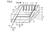
(オフ方向に対して垂直な直線に沿って並ぶハーフループの転位列)
図1および図3に示されるように、中央領域53には、オフ方向に対して垂直な直線に沿って並ぶ第1ハーフループ1の第1転位列2がある。第1転位列2は、複数の第1ハーフループ1から構成されている。オフ方向が第1方向101の場合、オフ方向に対して垂直な方向は第2方向102である。第1ハーフループ1は、第2主面30に露出する一対の貫通刃状転位を含む。中央領域53における第1転位列2の面密度は、10本/cm2以下である。好ましくは、中央領域53における第1転位列2の面密度は、8本/cm2以下であり、より好ましくは5本/cm2以下である。
(Half-loop dislocation sequence along a straight line perpendicular to the off direction)
As shown in FIGS. 1 and 3, in the
次に、転位列の面密度の測定方法について説明する。
まず、溶融KOH(水酸化カリウム)で中央領域53がエッチングされることにより、中央領域53にエッチピットが形成される。溶融KOHの温度は、たとえば515℃である。溶融KOHによるエッチング時間は、たとえば8分である。次に、光学顕微鏡を用いて中央領域53に形成されたエッチピットが観察される。中央領域53が、たとえば格子状に1cm×1cmの正方形領域に分割される。全ての正方形領域において転位列の面密度が測定される。中央領域53における第1転位列2の面密度は、10本/cm2以下であるとは、全ての正方形領域において第1転位列2の面密度が10本/cm2以下であることを意味する。なお、中央領域53の外周付近は、ラウンド状であるため正方形の領域に分割できない。転位列の面密度の計算に際して、このような正方形の領域に分割できない領域における面密度は考慮しない。
Next, a method for measuring the surface density of the dislocation row will be described.
First, the
図3に示されるように、第1ハーフループ1は、略U字型を有している。第1ハーフループ1の湾曲部は炭化珪素層20内に設けられている。一対の貫通刃状転位の端部3は第2主面30に露出している。第1ハーフループ1の湾曲部は、貫通刃状転位以外の転位であってもよい。炭化珪素エピタキシャル基板100は、基底面転位34を含んでいる。基底面転位34は、第1部分31と、第2部分32と、第3部分33とにより構成されている。第1部分31は、炭化珪素単結晶基板10中に存在する基底面転位である。第2部分32は、炭化珪素単結晶基板10と炭化珪素層20との界面に存在する界面転位である。第3部分33は、炭化珪素層20中に存在する基底面転位である。第1部分31は、第2部分32と繋がっている。第2部分32は、第3部分33と繋がっている。第1部分31は、炭化珪素単結晶基板10の第3主面13に露出する。第3部分33は、炭化珪素層20の第2主面30に露出する。言い換えれば、基底面転位34の一方の端部35は第2主面30に露出し、他方の端部は第3主面13に露出する。
As shown in FIG. 3, the
図3に示されるように、第1転位列2は、第1部分31を、第1部分31の伸展方向に沿って炭化珪素層20側に延長した仮想線37が第2主面30に露出した点36と、基底面転位34の一方の端部35との間に位置してもよい。言い換えれば、第1転位列2が含む複数の第1ハーフループ1の各々は、点36と端部35との間に位置していてもよい。つまり、第2主面30に対して垂直な方向から見て、第1転位列2は、仮想線37と第3部分33との間に位置していてもよい。
As shown in FIG. 3, in the
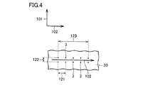
図4に示されるように、第2方向102において、第1転位列2の長さ123は、たとえば0.1mm以上50mm以下である。第1方向101において、一方の端部3と他方の端部3と間の距離122は、たとえば1μm以上10μm以下である。第2方向102において、隣り合う2つの第1ハーフループ1の間の距離121は、たとえば1μm以上100μm以下である。距離121は、距離122よりも長くてもよい。2つの端部3は、第1方向101上に位置していてもよい。隣り合う2つの第1ハーフループ間の間隔は、同じであってもよいし、異なっていてもよい。第2主面30に対して垂直な方向から見て、複数のハーフループ1の各々は、第2方向102に平行な直線と重なっている。第1転位列2の長手方向は、第2方向102である。第1転位列2の長手方向は、界面転位の伸展方向と平行であってもよい。
As shown in FIG. 4, in the
図5に示されるように、第2主面30に対して垂直な方向において、複数のハーフループ1の各々の深さは、ほぼ同じであってもよい。第1ハーフループ1の深さとは、第2主面30に対して垂直な方向におけるハーフループの長さである。第1ハーフループ1の深さは、炭化珪素層20の厚みより小さくてもよい。第1ハーフループ1は、炭化珪素単結晶基板10から離間していてもよい。
As shown in FIG. 5, in the direction perpendicular to the second
(オフ方向に対して傾斜する直線に沿って並ぶハーフループの転位列)
図1および図6に示されるように、中央領域53には、オフ方向に対して傾斜する直線に沿って並ぶ第2ハーフループ4の第2転位列5があってもよい。第2転位列5は、複数の第2ハーフループ4から構成されている。第2ハーフループ4は、第1方向101および第2方向102の双方に対して傾斜する直線に平行な第3方向103に沿って並んでいる。第2ハーフループ4は、第2主面30に露出する一対の貫通刃状転位を含む。中央領域53おいて、第1転位列2の面密度は、第2転位列5の面密度よりも低くてもよい。中央領域53における第2転位列5の面密度は、10本/cm2よりも高くてもよい。第1転位列2は、外周領域52の近くに多く存在し、第2転位列5は、中央領域53の中心付近に多く存在する傾向がある。
(Half-loop dislocation sequence lined up along a straight line that slopes in the off direction)
As shown in FIGS. 1 and 6, the
図6に示されるように、第2ハーフループ4は、略U字型を有している。第2ハーフループ4の湾曲部は炭化珪素層20内に設けられており、一対の貫通刃状転位の端部6が第2主面30に露出している。第2ハーフループ4の湾曲部は、貫通刃状転位以外の転位であってもよい。炭化珪素エピタキシャル基板100は、基底面転位44を含んでいる。基底面転位44は、第4部分41と、第5部分42と、第6部分43とにより構成されている。第4部分41は、炭化珪素単結晶基板10中に存在する基底面転位である。第5部分42は、炭化珪素単結晶基板10と炭化珪素層20との界面に存在する界面転位である。第6部分43は、炭化珪素層20中に存在する基底面転位である。第4部分41は、第5部分42と繋がっている。第5部分42は、第6部分43と繋がっている。第4部分41は、炭化珪素単結晶基板10の第3主面13に露出する。第6部分43は、炭化珪素層20の第2主面30に露出する。言い換えれば、基底面転位44の一方の端部45は第2主面30に露出し、他方の端部は第3主面13に露出する。第2主面30に対して垂直な方向から見て、第2転位列5は、第4部分41を、第4部分41の伸展方向に沿って炭化珪素層20側に延長した仮想線47と、第6部分43との間に位置していてもよい。言い換えれば、第2転位列5は、仮想線47が第2主面30に露出した点46と、基底面転位44の一方の端部45との間に位置してもよい。
As shown in FIG. 6, the
図7に示されるように、第3方向103において、第2転位列5の長さ126は、たとえば0.1mm以上50mm以下である。第3方向103に対して垂直な方向において、一方の端部6と他方の端部6と間の距離125は、たとえば1μm以上10μm以下である。第3方向103において、隣り合う2つの第2ハーフループ4の間の距離124は、たとえば1μm以上100μm以下である。距離124は、距離125よりも長くてもよい。2つの端部6は、第3方向103方向に対して垂直な直線上に位置していてもよい。第2主面30に対して垂直な方向から見て、複数の第2ハーフループ4の各々は、第3方向103に平行な直線と重なっている。隣り合う2つの第2ハーフループ間の間隔は、同じであってもよいし、異なっていてもよい。
As shown in FIG. 7, in the
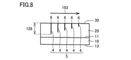
図8に示されるように、第2主面30に対して垂直な方向において、複数の第2ハーフループ4の各々の深さは、異なっていてもよい。第2ハーフループ4の深さとは、第2主面30に対して垂直な方向におけるハーフループの長さである。具体的には、第2ハーフループ4の深さは、オフ方向に向かって小さくなっていてもよい。言い換えれば、第2主面30に対して垂直な方向から見て、第4部分41に近い第2ハーフループ4の深さは、第6部分43に近い第2ハーフループ4の深さよりも大きい。第2ハーフループ4の深さは、炭化珪素層20の厚みより小さくてもよい。第2ハーフループ4は、炭化珪素単結晶基板10から離間していてもよい。
As shown in FIG. 8, the depth of each of the plurality of
(成膜装置)
次に、本実施形態に係る炭化珪素エピタキシャル基板100の製造方法で使用される製造装置200の構成について説明する。
(Film formation equipment)
Next, the configuration of the
図9に示されるように、製造装置200は、たとえばホットウォール方式のCVD(Chemical Vapor Deposition)装置である。製造装置200は、発熱体203、石英管204、断熱材205、誘導加熱コイル206および予備加熱機構211を主に有する。発熱体203に取り囲まれた空洞は、反応室201である。反応室201には、炭化珪素単結晶基板10を保持するサセプタプレート210が設けられている。サセプタプレート210は自転可能である。炭化珪素単結晶基板10は、第1主面11を上にして、サセプタプレート210に載せられる。
As shown in FIG. 9, the
発熱体203は、たとえば黒鉛製である。誘導加熱コイル206は、石英管204の外周に沿って巻回されている。誘導加熱コイル206に所定の交流電流を供給することにより、発熱体203が誘導加熱される。これにより反応室201が加熱される。
The
製造装置200は、ガス導入口207およびガス排気口208をさらに有する。ガス排気口208は、図示しない排気ポンプに接続されている。図9中の矢印は、ガスの流れを示している。キャリアガス、原料ガスおよびドーピングガスは、ガス導入口207から反応室201に導入され、ガス排気口208から排気される。反応室201内の圧力は、ガスの供給量と、ガスの排気量とのバランスによって調整され得る。
The
通常、サセプタプレート210および単結晶基板10は、反応室201の軸方向において、略中央に配置されている。図9に示されるように、本開示では、サセプタプレート210および単結晶基板10が、反応室201の中央よりも下流側、すなわちガス排気口208側に配置されていてもよい。原料ガスが単結晶基板10に到達するまでに、原料ガスの分解反応を十分に進行させるためである。これにより単結晶基板10の面内においてC/Si比の分布が均一になることが期待される。
Normally, the
ドーパントガスであるアンモニアガスは、反応室201に供給される前に、十分に加熱し、予め熱分解させておくことが望ましい。これにより炭化珪素層20において、窒素(ドーパント)密度の面内均一性が向上することが期待できる。図9に示されるように、反応室201の上流側に予備加熱機構211が設けられていてもよい。予備加熱機構211において、アンモニアガスを事前に加熱することができる。予備加熱機構211は、たとえば1300℃以上に加熱された部屋を備えている。アンモニアガスは、予備加熱機構211の内部を通過する際、十分に熱分解され、その後反応室201へと供給される。こうした構成により、ガスの流れに大きな乱れを生じさせることなく、アンモニアガスの熱分解を行うことができる。
Ammonia gas, which is a dopant gas, is preferably sufficiently heated and thermally decomposed in advance before being supplied to the
(炭化珪素エピタキシャル基板の製造方法)
次に、本実施形態に係る炭化珪素エピタキシャル基板の製造方法について説明する。
(Manufacturing method of silicon carbide epitaxial substrate)
Next, a method for manufacturing the silicon carbide epitaxial substrate according to the present embodiment will be described.
まず、たとえば昇華法により、ポリタイプ4Hの炭化珪素単結晶が製造される。次に、たとえばワイヤーソーによって、炭化珪素単結晶をスライスすることにより、炭化珪素単結晶基板10が準備される(図10および図11参照)。炭化珪素単結晶基板10は、第1主面11と、第1主面11と反対側の第3主面13とを有する。図11に示されるように、第1主面11は、{0001}面がオフ方向に傾斜した面である。
First, for example, a polytype 4H silicon carbide single crystal is produced by a sublimation method. Next, the silicon carbide
具体的には、第1主面11は、たとえば{0001}面から4°以下傾斜した面である。第1主面11は、(0001)面が4°以下傾斜した面であってもよいし、(000−1)面が4°以下傾斜した面であってもよい。{0001}面からの傾斜角(オフ角)は、1°以上であってもよいし、2°以上であってもよい。オフ角は、3°以下であってもよい。オフ方向は、たとえば<11−20>方向であってもよいし、<1−100>方向であってもよいし、<11−20>方向と<1−100>方向とに挟まれた方向であってもよい。
Specifically, the first
次に、炭化珪素単結晶基板10が、前述した製造装置200内に配置される。具体的には、炭化珪素単結晶基板10は、第1主面11がサセプタプレート210から露出するように、サセプタプレート210の凹部に配置される。次に、炭化珪素単結晶基板10上に炭化珪素層20がエピタキシャル成長によって形成される。たとえば反応室201の圧力が大気圧から1×10⁻⁶Pa程度に低減された後、炭化珪素単結晶基板10の昇温が開始される。昇温の途中において、キャリアガスである水素(H2)ガスが、反応室201に導入される。
Next, the silicon carbide
反応室201内の温度がたとえば1600℃程度となった後、原料ガスおよびドーピングガスが反応室201に導入される。原料ガスは、Si源ガスおよびC源ガスを含む。Si源ガスとして、たとえばシラン(SiH4)ガス用いることができる。C源ガスとして、たとえばプロパン(C3H8)ガスを用いることができる。シランガスの流量およびプロパンガスの流量は、たとえば46sccmおよび14sccmである。水素に対するシランガスの体積比率は、たとえば0.04%である。原料ガスのC/Si比は、たとえば0.9である。
After the temperature in the
ドーピングガスとして、たとえばアンモニア(NH3)ガスが用いられる。アンモニアガスは、三重結合を有する窒素ガスに比べて熱分解されやすい。アンモニアガスを用いることにより、キャリア濃度の面内均一性の向上が期待できる。水素ガスに対するアンモニアガスの濃度は、たとえば1ppmである。アンモニアガスは、反応室201に導入される前に、予備加熱機構211で、予め熱分解させておくことが望ましい。予備加熱機構211により、アンモニアガスは、たとえば1300℃以上に加熱される。
As the doping gas, for example, ammonia (NH 3 ) gas is used. Ammonia gas is more easily pyrolyzed than nitrogen gas having a triple bond. By using ammonia gas, improvement of in-plane uniformity of carrier concentration can be expected. The concentration of ammonia gas with respect to hydrogen gas is, for example, 1 ppm. It is desirable that the ammonia gas is pyrolyzed in advance by the
炭化珪素単結晶基板10が1600℃程度に加熱された状態で、キャリアガス、原料ガスおよびドーピングガスが反応室201に導入されることで、炭化珪素単結晶基板10上に炭化珪素層20がエピタキシャル成長により形成される。炭化珪素層20がエピタキシャル成長している間、サセプタプレート210は回転軸212(図9参照)の周りを回転している。サセプタプレート210の平均回転数は、たとえば20rpmである。以上により、炭化珪素単結晶基板10上に炭化珪素層20がエピタキシャル成長によって形成される。
A carrier gas, a raw material gas, and a doping gas are introduced into the
図12に示されるように、炭化珪素層20の成長工程において、炭化珪素単結晶基板10の温度が、第0時点(T0)から第3時点(T3)まで第1温度(A1)に維持される。第1温度(A1)は、たとえば、1600℃である、第0時点(T0)は、反応室201に対する原料ガスおよびドーピングガスの導入が開始された時点である。第0時点(T0)において、炭化珪素単結晶基板10上に炭化珪素層20の形成が実質的に開始される。第3時点(T3)は、反応室201に対する原料ガスおよびドーピングガスの導入が終了した時点である。第3時点(T3)において、炭化珪素単結晶基板10上に炭化珪素層20の形成が実質的に終了する。好ましくは、炭化珪素層20の成長工程において、炭化珪素単結晶基板10の面内方向の温度が均一に維持される。具体的には、第0時点(T0)から第3時点(T3)までの間、炭化珪素単結晶基板10の第1主面11における最高温度と最低温度との差が10℃以下に維持される。
As shown in FIG. 12, in the growth step of the
次に、炭化珪素単結晶基板10のある領域XIII上における炭化珪素層20の部分の成長工程について詳細に説明する。
Next, the growth step of the portion of the
図10および図13に示されるように、第0時点(T0)において、炭化珪素単結晶基板10内のある領域XIIIには、{0001}面上に伸展する基底面転位34が存在している。基底面転位34の一方の端部は、第1主面11に露出し、他方の端部は第3主面13に露出している。基底面転位34は、オフ方向である第1方向101に沿って伸展している。
As shown in FIGS. 10 and 13, at the 0th time point (T0), a
図14に示されるように、第1時点(T1)において、炭化珪素層20の一部が炭化珪素単結晶基板10上に形成される。基底面転位34は、炭化珪素単結晶基板10から炭化珪素層20に伝播する。基底面転位34は、第1方向101に沿って炭化珪素層20中を伸展する。基底面転位34の一方の端部は、炭化珪素層20の表面に露出し、他方の端部は第3主面13に露出している。
As shown in FIG. 14, at the first time point (T1), a part of the
図15に示されるように、基底面転位34は、炭化珪素層20の成長に伴って、炭化珪素層20中をさらに伸展する。第1時点(T1)よりも後の第3時点(T3)において、基底面転位34の一方の端部は炭化珪素層20の第2主面30に露出し、他方の端部は炭化珪素単結晶基板10の第3主面13に露出している。以上により、炭化珪素層20の形成が実質的に完了する。
As shown in FIG. 15, the
次に、炭化珪素エピタキシャル基板100の冷却工程について説明する。
図12に示されるように、成長工程終了後、冷却工程が実施される。第3時点(T3)から第7時点(T7)までが冷却工程である。冷却工程において、炭化珪素単結晶基板10と炭化珪素層20とを含む炭化珪素エピタキシャル基板100が冷却される。たとえば、第3時点(T3)から第6時点(T6)にかけて、炭化珪素エピタキシャル基板100の温度は、第1温度(A1)から第2温度(A2)まで低下する。第3時点(T3)から第6時点(T6)までの時間は、たとえば60分である。第1温度(A1)は、たとえば1600℃であり、第2温度(A2)は、たとえば100℃である。つまり、炭化珪素エピタキシャル基板100の冷却速度は、たとえば(1600−100)℃/1h=1500℃/hである。第1温度(A1)から第2温度(A2)までの冷却速度は、1500℃/h以下であってもよいし、1300℃/h以下であってもよいし、1000℃/h以下であってもよい。
Next, the cooling process of the silicon
As shown in FIG. 12, a cooling step is carried out after the growth step is completed. The cooling process is from the third time point (T3) to the seventh time point (T7). In the cooling step, the silicon
図16に示されるように、冷却工程において、炭化珪素層20中に第1ハーフループ1から構成される第1転位列2が形成される場合がある。第1転位列2は、炭化珪素層20中の基底面転位の第3部分33が、オフ方向とは垂直な第2方向102にスライドすることにより発生すると考えられる。成長工程における基底面転位34(図15参照)は、冷却工程において第1部分31と第2部分32と第3部分33とにより構成される基底面転位34(図16)に変化するとともに、複数の第1ハーフループ1を形成する。言い換えれば、第1ハーフループ1は基底面転位34に起因して発生する。
As shown in FIG. 16, in the cooling step, the
好ましくは、炭化珪素エピタキシャル基板100の冷却工程において、炭化珪素エピタキシャル基板100の面内方向の温度が均一に維持される。具体的には、第3時点(T3)から第6時点(T6)までの間、炭化珪素エピタキシャル基板100の第2主面30における最高温度と最低温度との差が10℃以下に維持される。以上のように、冷却工程における炭化珪素エピタキシャル基板100の冷却速度を低くすることにより、炭化珪素エピタキシャル基板100の面内方向の温度の均一性を向上することができる。結果として、炭化珪素エピタキシャル基板100内の応力を緩和することで、オフ方向に対して垂直な直線に沿って並ぶ第1ハーフループ1の第1転位列2の発生を抑制することができる。
Preferably, in the cooling step of the silicon
次に、第5時点(T5)から第6時点(T6)にかけて、炭化珪素エピタキシャル基板100の温度は、第2温度(A2)から第3温度(A3)まで低下する。第3温度(A3)は、たとえば室温である。炭化珪素エピタキシャル基板100の温度が室温付近になった後、炭化珪素エピタキシャル基板100が反応室201から取り出される。以上のようにして、炭化珪素エピタキシャル基板100が完成する(図1参照)。
Next, from the fifth time point (T5) to the sixth time point (T6), the temperature of the silicon
図20に示されるように、冷却工程において、反応室201内の圧力が低減されてもよい。たとえば、第3時点(T3)から第4時点(T4)にかけて、反応室201内の圧力は、第1圧力(B1)から第2圧力(B2)まで低下する。第1圧力(B1)は、たとえば100mbar(10kPa)であり、第2圧力(B2)は、たとえば10mbar(1kPa)である。第3時点(T3)から第4時点(T4)までの時間は、たとえば10分である。つまり、反応室201内の圧力の低下速度は、(10−1)kPa/10分=0.9kPa/分である。反応室201内の圧力の低減速度は、0.9kPa/分以上であってもよし、1.2kPa/分以上であってもよいし、1.5kPa/分以上であってもよい。冷却工程において反応室201の圧力を急速に低減することにより、反応室201内を外部から断熱し、炭化珪素エピタキシャル基板100の冷却速度を低減することができる。
As shown in FIG. 20, the pressure in the
反応室201内の圧力は、たとえばキャリアガスの流量を低減することにより低減し得る。たとえば、成長工程におけるキャリアガスの流量が120slmであり、冷却工程におけるキャリアガスの流量が12slmであってもよい。成長工程において、反応室201にはキャリアガス、ドーパントガスおよび原料ガスが供給されている。冷却工程において、反応室201にはキャリアガスのみが供給されていてもよい。キャリアガスの流量は、成長工程終了直後に低減されてもよいし、冷却工程において成長工程における流量を一定時間維持した後低減されてもよい。
The pressure in the
次に、炭化珪素単結晶基板10のある領域XVI上における炭化珪素層20の部分の成長工程について詳細に説明する。
Next, the growth step of the portion of the
図10および図17に示されるように、第0時点(T0)において、炭化珪素単結晶基板10内のある領域XVIIには、{0001}面上に存在する基底面転位44が存在していてもよい。基底面転位44の一方の端部は、第1主面11に露出し、他方の端部は第3主面13に露出している。基底面転位は、オフ方向である第1方向101に沿って伸展している。
As shown in FIGS. 10 and 17, at the 0th time point (T0), a
図18に示されるように、第1時点(T1)において、基底面転位44に起因して第2ハーフループ4が発生する。第2ハーフループ4の2つの端部は、炭化珪素層20の表面に露出する。炭化珪素層20中を伸展していた基底面転位の第6部分43は、第2方向(図18中の矢印の方向)にシフトする。結果として、基底面転位44は、炭化珪素単結晶基板10中に位置する第4部分41と、炭化珪素単結晶基板10と炭化珪素層20との界面に位置し、かつ第2方向に伸展する第5部分42と、炭化珪素層20中に位置する第6部分43とに転換され、第2ハーフループ4を発生させる。基底面転位44の一方の端部は、炭化珪素層20の表面に露出し、他方の端部は第3主面13に露出している。
As shown in FIG. 18, at the first time point (T1), the
図19に示されるように、第2時点(T2)において、基底面転位44に起因して、もう一つの第2ハーフループ4が発生する。もう一つの第2ハーフループ4は、先に発生した第2ハーフループ4よりも第1方向101側であってかつ第2方向102側に発生する。先に発生した第2ハーフループ4の深さは、後に発生した第2ハーフループ4の深さよりも大きい。第1時点(T1)において炭化珪素層20中に存在していた基底面転位の第6部分43は、さらに第2方向(図19中の矢印の方向)にシフトする。第6部分43は、炭化珪素層20の表面に露出する。以上のようにして、オフ方向とは傾斜した直線に沿って、複数の第2ハーフループ4が形成される。時間の経過につれて、第2ハーフループ4の数は増加する。第3時点(T3)において、オフ方向に対して傾斜する直線に沿って並ぶ第2ハーフループ4の第2転位列5が形成される(図6参照)。以上のように、第2転位列5は、炭化珪素層の形成工程(つまり成長工程)において形成される。言い換えれば、炭化珪素エピタキシャル基板100の冷却工程においては、第2転位列5は、発生することもなく、消滅することもないと考えられる。
As shown in FIG. 19, at the second time point (T2), another
(炭化珪素半導体装置の製造方法)
次に、本実施形態に係る炭化珪素半導体装置300の製造方法について説明する。
(Manufacturing method of silicon carbide semiconductor device)
Next, a method for manufacturing the silicon
本実施形態に係る炭化珪素半導体装置の製造方法は、エピタキシャル基板準備工程(S10:図21)と、基板加工工程(S20:図21)とを主に有する。 The method for manufacturing a silicon carbide semiconductor device according to the present embodiment mainly includes an epitaxial substrate preparation step (S10: FIG. 21) and a substrate processing step (S20: FIG. 21).
まず、エピタキシャル基板準備工程(S10:図21)が実施される。具体的には、前述した炭化珪素エピタキシャル基板の製造方法によって、炭化珪素エピタキシャル基板100が準備される(図1参照)。エピタキシャル基板準備工程(S10:図21)は、炭化珪素単結晶基板10上にバッファ層21を形成する工程を含んでいてもよい。
First, the epitaxial substrate preparation step (S10: FIG. 21) is carried out. Specifically, the silicon
次に、基板加工工程(S20:図21)が実施される。具体的には、炭化珪素エピタキシャル基板を加工することにより、炭化珪素半導体装置が製造される。「加工」には、たとえば、イオン注入、熱処理、エッチング、酸化膜形成、電極形成、ダイシング等の各種加工が含まれる。すなわち基板加工ステップは、イオン注入、熱処理、エッチング、酸化膜形成、電極形成およびダイシングのうち、少なくともいずれかの加工を含むものであってもよい。 Next, a substrate processing step (S20: FIG. 21) is carried out. Specifically, a silicon carbide semiconductor device is manufactured by processing a silicon carbide epitaxial substrate. “Processing” includes, for example, various processes such as ion implantation, heat treatment, etching, oxide film formation, electrode formation, and dicing. That is, the substrate processing step may include processing at least one of ion implantation, heat treatment, etching, oxide film formation, electrode formation and dicing.
以下では、炭化珪素半導体装置の一例としてのMOSFET(Metal Oxide Semiconductor Field Effect Transistor)の製造方法を説明する。基板加工工程(S20:図21)は、イオン注入工程(S21:図21)、酸化膜形成工程(S22:図21)、電極形成工程(S23:図21)およびダイシング工程(S24:図21)を含む。 Hereinafter, a method for manufacturing a MOSFET (Metal Oxide Semiconductor Field Effect Transistor) as an example of a silicon carbide semiconductor device will be described. The substrate processing step (S20: FIG. 21) includes an ion implantation step (S21: FIG. 21), an oxide film forming step (S22: FIG. 21), an electrode forming step (S23: FIG. 21), and a dicing step (S24: FIG. 21). including.
まず、イオン注入工程(S21:図21)が実施される。開口部を有するマスク(図示せず)が形成された第2主面30に対して、たとえばアルミニウム(Al)等のp型不純物が注入される。これにより、p型の導電型を有するボディ領域132が形成される。次に、ボディ領域132内の所定位置に、たとえばリン(P)等のn型不純物が注入される。これにより、n型の導電型を有するソース領域133が形成される。次に、アルミニウム等のp型不純物がソース領域133内の所定位置に注入される。これにより、p型の導電型を有するコンタクト領域134が形成される(図22参照)。
First, the ion implantation step (S21: FIG. 21) is carried out. A p-type impurity such as aluminum (Al) is injected into the second
炭化珪素層20において、ボディ領域132、ソース領域133およびコンタクト領域134以外の部分は、ドリフト領域131となる。ソース領域133は、ボディ領域132によってドリフト領域131から隔てられている。イオン注入は、炭化珪素エピタキシャル基板100を300℃以上600℃以下程度に加熱して行われてもよい。イオン注入の後、炭化珪素エピタキシャル基板100に対して活性化アニールが行われる。活性化アニールにより、炭化珪素層20に注入された不純物が活性化し、各領域においてキャリアが生成される。活性化アニールの雰囲気は、たとえばアルゴン(Ar)雰囲気でもよい。活性化アニールの温度は、たとえば1800℃程度でもよい。活性化アニールの時間は、たとえば30分程度でもよい。
In the
次に、酸化膜形成工程(S22:図21)が実施される。たとえば炭化珪素エピタキシャル基板100が酸素を含む雰囲気中において加熱されることにより、第2主面30上に酸化膜136が形成される(図23参照)。酸化膜136は、たとえば二酸化珪素(SiO2)等から構成される。酸化膜136は、ゲート絶縁膜として機能する。熱酸化処理の温度は、たとえば1300℃程度でもよい。熱酸化処理の時間は、たとえば30分程度でもよい。
Next, an oxide film forming step (S22: FIG. 21) is carried out. For example, when the silicon
酸化膜136が形成された後、さらに窒素雰囲気中で熱処理が行なわれてもよい。たとえば、一酸化窒素(NO)、亜酸化窒素(N2O)等の雰囲気中、1100℃程度で1時間程度、熱処理が実施されてもよい。さらにその後、アルゴン雰囲気中で熱処理が行なわれてもよい。たとえば、アルゴン雰囲気中、1100〜1500℃程度で、1時間程度、熱処理が行われてもよい。
After the
次に、電極形成工程(S23:図21)が実施される。第1電極141は、酸化膜136上に形成される。第1電極141は、ゲート電極として機能する。第1電極141は、たとえばCVD法により形成される。第1電極141は、たとえば不純物を含有し導電性を有するポリシリコン等から構成される。第1電極141は、ソース領域133およびボディ領域132に対面する位置に形成される。
Next, the electrode forming step (S23: FIG. 21) is carried out. The
次に、第1電極141を覆う層間絶縁膜137が形成される。層間絶縁膜137は、たとえばCVD法により形成される。層間絶縁膜137は、たとえば二酸化珪素等から構成される。層間絶縁膜137は、第1電極141と酸化膜136とに接するように形成される。次に、所定位置の酸化膜136および層間絶縁膜137がエッチングによって除去される。これにより、ソース領域133およびコンタクト領域134が、酸化膜136から露出する。
Next, an
たとえばスパッタリング法により当該露出部に第2電極142が形成される。第2電極142はソース電極として機能する。第2電極142は、たとえばチタン、アルミニウムおよびシリコン等から構成される。第2電極142が形成された後、第2電極142と炭化珪素エピタキシャル基板100が、たとえば900〜1100℃程度の温度で加熱される。これにより、第2電極142と炭化珪素エピタキシャル基板100とがオーミック接触するようになる。次に、第2電極142に接するように、配線層138が形成される。配線層138は、たとえばアルミニウムを含む材料から構成される。
For example, a
次に、第3主面13に第3電極143が形成される。第3電極143は、ドレイン電極として機能する。第3電極143は、たとえばニッケルおよびシリコンを含む合金(たとえばNiSi等)から構成される。
Next, the
次に、ダイシング工程(S24:図21)が実施される。たとえば炭化珪素エピタキシャル基板100がダイシングラインに沿ってダイシングされることにより、炭化珪素エピタキシャル基板100が複数の半導体チップに分割される。以上より、炭化珪素半導体装置300が製造される(図24参照)。
Next, a dicing step (S24: FIG. 21) is carried out. For example, the silicon
上記において、MOSFETを例示して、本開示に係る炭化珪素半導体装置の製造方法を説明したが、本開示に係る製造方法はこれに限定されない。本開示に係る製造方法は、たとえばIGBT(Insulated Gate Bipolar Transistor)、SBD(Schottky Barrier Diode)、サイリスタ、GTO(Gate Turn Off thyristor)、PiNダイオード等の各種炭化珪素半導体装置に適用可能である。 In the above, the manufacturing method of the silicon carbide semiconductor device according to the present disclosure has been described by exemplifying the MOSFET, but the manufacturing method according to the present disclosure is not limited to this. The manufacturing method according to the present disclosure can be applied to various silicon carbide semiconductor devices such as IGBTs (Insulated Gate Bipolar Transformers), SBDs (Schottky Barrier Diodes), thyristors, GTOs (Gate Turn Off thyristors), and PiN diodes.
今回開示された実施形態はすべての点で例示であって、制限的なものではないと考えられるべきである。本発明の範囲は上記した実施形態ではなく特許請求の範囲によって示され、特許請求の範囲と均等の意味、および範囲内でのすべての変更が含まれることが意図される。 The embodiments disclosed this time should be considered as exemplary in all respects and not restrictive. The scope of the present invention is shown not by the above-described embodiment but by the scope of claims, and is intended to include the meaning equivalent to the scope of claims and all modifications within the scope.
1 第1ハーフループ(ハーフループ)、2 第1転位列(転位列)、3,6,35,45 端部、4 第2ハーフループ、5 第2転位列、10 炭化珪素単結晶基板、11 第1主面、13 第3主面、14 第4主面(面)、20 炭化珪素層、21 バッファ層、30 第2主面、31 第1部分、32 第2部分、33 第3部分、34,44 基底面転位、37,47 仮想線、41 第4部分、42 第5部分、43 第6部分、52 外周領域、53 中央領域、54 外縁、100 炭化珪素エピタキシャル基板、101 第1方向、102 第2方向、103 第3方向、111 最大径、131 ドリフト領域、132 ボディ領域、133 ソース領域、134 コンタクト領域、136 酸化膜、137 層間絶縁膜、138 配線層、141 第1電極、142 第2電極、143 第3電極、200 製造装置、201 反応室、203 発熱体、204 石英管、205 断熱材、206 誘導加熱コイル、207 ガス導入口、208 ガス排気口、210 サセプタプレート、211 予備加熱機構、212 回転軸、300 炭化珪素半導体装置。 1 1st half loop (half loop), 2 1st dislocation row (dislocation row), 3, 6, 35, 45 ends, 4 2nd half loop, 5 2nd dislocation row, 10 Silicon carbide single crystal substrate, 11 1st main surface, 13 3rd main surface, 14 4th main surface (plane), 20 silicon carbide layer, 21 buffer layer, 30 2nd main surface, 31 1st part, 32 2nd part, 33 3rd part, 34,44 dislocations, 37,47 virtual lines, 41 4th part, 42 5th part, 43 6th part, 52 outer peripheral region, 53 central region, 54 outer edge, 100 silicon carbide epitaxial substrate, 101 1st direction, 102 2nd direction, 103 3rd direction, 111 maximum diameter, 131 drift area, 132 body area, 133 source area, 134 contact area, 136 oxide film, 137 interlayer insulating film, 138 wiring layer, 141 first electrode, 142th 2 electrodes, 143 3rd electrodes, 200 manufacturing equipment, 201 reaction chamber, 203 heating element, 204 quartz tube, 205 insulation material, 206 induction heating coil, 207 gas inlet, 208 gas exhaust port, 210 susceptor plate, 211 preheating Mechanism, 212 rotating shaft, 300 silicon carbide semiconductor device.
Claims (6)
前記第1主面上の炭化珪素層とを備え、
前記炭化珪素層は、前記炭化珪素単結晶基板と接する面と反対側の第2主面を含み、
前記第2主面は、{0001}面がオフ方向に傾斜した面であり、
前記第2主面の最大径は、100mm以上であり、
前記第2主面は、前記第2主面の外縁から3mm以内の外周領域と、前記外周領域に取り囲まれた中央領域とを有し、
前記中央領域には、前記オフ方向に対して垂直な直線に沿って並ぶ第1ハーフループの第1転位列があり、
前記第1ハーフループは、前記第2主面に露出する一対の貫通刃状転位を含み、
前記中央領域における前記第1転位列の面密度は、8本/cm2以下であり、
前記中央領域には、前記オフ方向に対して傾斜する直線に沿って並ぶ第2ハーフループの第2転位列があり、
前記第2ハーフループは、前記第2主面に露出する一対の貫通刃状転位を含み、
前記中央領域おいて、前記第1転位列の面密度は、前記第2転位列の面密度よりも低い、炭化珪素エピタキシャル基板。 A silicon carbide single crystal substrate having a first main surface and
With a silicon carbide layer on the first main surface,
The silicon carbide layer includes a second main surface opposite to the surface in contact with the silicon carbide single crystal substrate.
The second main surface is a surface in which the {0001} surface is inclined in the off direction.
The maximum diameter of the second main surface is 100 mm or more.
The second main surface has an outer peripheral region within 3 mm from the outer edge of the second main surface and a central region surrounded by the outer peripheral region.
In the central region, there is a first dislocation sequence of the first half loop that is aligned along a straight line perpendicular to the off direction.
The first half loop contains a pair of through-blade dislocations exposed on the second main surface.
The areal density of the first dislocation arrays in the central region state, and are eight / cm 2 or less,
In the central region, there is a second dislocation sequence of the second half loop arranged along a straight line inclined with respect to the off direction.
The second half loop contains a pair of through-blade dislocations exposed on the second main surface.
A silicon carbide epitaxial substrate in which the surface density of the first dislocation row is lower than the areal density of the second dislocation row in the central region .
前記炭化珪素エピタキシャル基板を加工する工程とを備える、炭化珪素半導体装置の製造方法。 The step of preparing the silicon carbide epitaxial substrate according to any one of claims 1 to 5 .
A method for manufacturing a silicon carbide semiconductor device, comprising a step of processing the silicon carbide epitaxial substrate.
Applications Claiming Priority (2)
| Application Number | Priority Date | Filing Date | Title |
|---|---|---|---|
| JP2015199565 | 2015-10-07 | ||
| JP2015199565 | 2015-10-07 |
Related Parent Applications (1)
| Application Number | Title | Priority Date | Filing Date |
|---|---|---|---|
| JP2016560603A Division JP6061060B1 (en) | 2015-10-07 | 2016-07-04 | Silicon carbide epitaxial substrate and method for manufacturing silicon carbide semiconductor device |
Related Child Applications (1)
| Application Number | Title | Priority Date | Filing Date |
|---|---|---|---|
| JP2020191406A Division JP7052851B2 (en) | 2015-10-07 | 2020-11-18 | Method for manufacturing silicon carbide epitaxial substrate and silicon carbide semiconductor device |
Publications (3)
| Publication Number | Publication Date |
|---|---|
| JP2017071551A JP2017071551A (en) | 2017-04-13 |
| JP2017071551A5 JP2017071551A5 (en) | 2019-07-04 |
| JP6798293B2 true JP6798293B2 (en) | 2020-12-09 |
Family
ID=58487499
Family Applications (2)
| Application Number | Title | Priority Date | Filing Date |
|---|---|---|---|
| JP2016238507A Active JP6798293B2 (en) | 2015-10-07 | 2016-12-08 | Method for manufacturing silicon carbide epitaxial substrate and silicon carbide semiconductor device |
| JP2020191406A Active JP7052851B2 (en) | 2015-10-07 | 2020-11-18 | Method for manufacturing silicon carbide epitaxial substrate and silicon carbide semiconductor device |
Family Applications After (1)
| Application Number | Title | Priority Date | Filing Date |
|---|---|---|---|
| JP2020191406A Active JP7052851B2 (en) | 2015-10-07 | 2020-11-18 | Method for manufacturing silicon carbide epitaxial substrate and silicon carbide semiconductor device |
Country Status (5)
| Country | Link |
|---|---|
| US (1) | US20170275779A1 (en) |
| JP (2) | JP6798293B2 (en) |
| CN (1) | CN108138360B (en) |
| DE (1) | DE112016004600T5 (en) |
| WO (1) | WO2017061154A1 (en) |
Families Citing this family (9)
| Publication number | Priority date | Publication date | Assignee | Title |
|---|---|---|---|---|
| JP2001189692A (en) * | 1999-12-28 | 2001-07-10 | Matsushita Electric Ind Co Ltd | Receiver and gain control method |
| WO2017061154A1 (en) * | 2015-10-07 | 2017-04-13 | 住友電気工業株式会社 | Silicon carbide expitaxial substrate and method for manufacturing silicon carbide semiconductor device |
| US10526699B2 (en) | 2017-09-08 | 2020-01-07 | Sumitomo Electric Industries, Ltd. | Silicon carbide epitaxial substrate and method for manufacturing silicon carbide semiconductor device |
| DE102018106967B3 (en) * | 2018-03-23 | 2019-05-23 | Infineon Technologies Ag | SILICON CARBIDE SEMICONDUCTOR ELEMENT and semiconductor diode |
| US20210320005A1 (en) * | 2018-07-20 | 2021-10-14 | Sumitomo Electric Industries, Ltd. | Silicon carbide epitaxial substrate and method for manufacturing silicon carbide semiconductor device |
| CN113272480A (en) * | 2019-01-08 | 2021-08-17 | 住友电气工业株式会社 | Silicon carbide recycled substrate and method for manufacturing silicon carbide semiconductor device |
| JP7319502B2 (en) * | 2020-01-09 | 2023-08-02 | 株式会社東芝 | Silicon carbide substrate manufacturing method, semiconductor device manufacturing method, silicon carbide substrate, and semiconductor device |
| EP3943644A1 (en) * | 2020-07-21 | 2022-01-26 | SiCrystal GmbH | Sic crystals with an optimal orientation of lattice planes for fissure reduction and method of producing same |
| EP3943645A1 (en) * | 2020-07-21 | 2022-01-26 | SiCrystal GmbH | Sic crystalline substrates with an optimal orientation of lattice planes for fissure reduction and method of producing same |
Family Cites Families (60)
| Publication number | Priority date | Publication date | Assignee | Title |
|---|---|---|---|---|
| US40103A (en) * | 1863-09-29 | Improvement in quartz-crushers | ||
| US81910A (en) * | 1868-09-08 | keltum | ||
| US71301A (en) * | 1867-11-26 | Improvement in gang-ploughs | ||
| US51301A (en) * | 1865-12-05 | Improvement in mowing-machines | ||
| US53517A (en) * | 1866-03-27 | Improvement in sealing boxes | ||
| US93518A (en) * | 1869-08-10 | Improvement in stuffing-boxes | ||
| US33503A (en) * | 1861-10-15 | Improvement in railroad-rails | ||
| US123502A (en) * | 1872-02-06 | Improvement in hoes | ||
| US5679153A (en) * | 1994-11-30 | 1997-10-21 | Cree Research, Inc. | Method for reducing micropipe formation in the epitaxial growth of silicon carbide and resulting silicon carbide structures |
| US6534026B2 (en) * | 2000-02-15 | 2003-03-18 | The Fox Group, Inc. | Low defect density silicon carbide |
| US6863728B2 (en) * | 2001-02-14 | 2005-03-08 | The Fox Group, Inc. | Apparatus for growing low defect density silicon carbide |
| DE10247017B4 (en) * | 2001-10-12 | 2009-06-10 | Denso Corp., Kariya-shi | SiC single crystal, a method of producing a SiC single crystal, SiC wafers with an epitaxial film, and a method of producing a SiC wafer having an epitaxial film |
| WO2003078702A1 (en) * | 2002-03-19 | 2003-09-25 | Central Research Institute Of Electric Power Industry | METHOD FOR PREPARING SiC CRYSTAL AND SiC CRYSTAL |
| US6869480B1 (en) * | 2002-07-17 | 2005-03-22 | The United States Of America As Represented By The United States National Aeronautics And Space Administration | Method for the production of nanometer scale step height reference specimens |
| JP3764462B2 (en) * | 2003-04-10 | 2006-04-05 | 株式会社豊田中央研究所 | Method for producing silicon carbide single crystal |
| US7230274B2 (en) * | 2004-03-01 | 2007-06-12 | Cree, Inc | Reduction of carrot defects in silicon carbide epitaxy |
| WO2005093796A1 (en) * | 2004-03-26 | 2005-10-06 | The Kansai Electric Power Co., Inc. | Bipolar semiconductor device and process for producing the same |
| DE102005017814B4 (en) * | 2004-04-19 | 2016-08-11 | Denso Corporation | Silicon carbide semiconductor device and process for its production |
| EP1619276B1 (en) * | 2004-07-19 | 2017-01-11 | Norstel AB | Homoepitaxial growth of SiC on low off-axis SiC wafers |
| US7314520B2 (en) * | 2004-10-04 | 2008-01-01 | Cree, Inc. | Low 1c screw dislocation 3 inch silicon carbide wafer |
| EP1933386B1 (en) * | 2005-09-14 | 2012-11-07 | Central Research Institute of Electric Power Industry | Process for producing silicon carbide semiconductor device |
| JP5070691B2 (en) * | 2005-10-03 | 2012-11-14 | 住友電気工業株式会社 | Silicon carbide substrate and vertical semiconductor device |
| WO2008015766A1 (en) * | 2006-08-04 | 2008-02-07 | The Kansai Electric Power Co., Inc. | Method for recovering forward voltage of bipolar semiconductor device, method for reducing lamination defect and bipolar semiconductor device |
| WO2009035095A1 (en) * | 2007-09-12 | 2009-03-19 | Showa Denko K.K. | EPITAXIAL SiC SINGLE CRYSTAL SUBSTRATE AND METHOD FOR MANUFACTURING EPITAXIAL SiC SINGLE CRYSTAL SUBSTRATE |
| US8652255B2 (en) * | 2007-10-12 | 2014-02-18 | The United States Of America, As Represented By The Secretary Of The Navy | Method of producing epitaxial layers with low basal plane dislocation concentrations |
| JP5504597B2 (en) * | 2007-12-11 | 2014-05-28 | 住友電気工業株式会社 | Silicon carbide semiconductor device and manufacturing method thereof |
| JP4978637B2 (en) * | 2009-02-12 | 2012-07-18 | 株式会社デンソー | Method for producing silicon carbide single crystal |
| JP2010184833A (en) * | 2009-02-12 | 2010-08-26 | Denso Corp | Silicon carbide single crystal substrate and silicon carbide single crystal epitaxial wafer |
| CA2761473A1 (en) * | 2009-05-11 | 2010-11-18 | Sumitomo Electric Industries, Ltd. | Semiconductor device |
| US10256094B2 (en) * | 2009-08-20 | 2019-04-09 | The Government Of The United States Of America, As Represented By The Secretary Of The Navy | Reduction of basal plane dislocations in epitaxial SiC using an in-situ etch process |
| US9464366B2 (en) * | 2009-08-20 | 2016-10-11 | The United States Of America, As Represented By The Secretary Of The Navy | Reduction of basal plane dislocations in epitaxial SiC |
| US10256090B2 (en) * | 2009-08-20 | 2019-04-09 | The United States Of America, As Represented By The Secretary Of The Navy | Reduction of basal plane dislocations in epitaxial SiC using an in-situ etch process |
| JP4959763B2 (en) * | 2009-08-28 | 2012-06-27 | 昭和電工株式会社 | SiC epitaxial wafer and manufacturing method thereof |
| JP4887418B2 (en) * | 2009-12-14 | 2012-02-29 | 昭和電工株式会社 | Method for manufacturing SiC epitaxial wafer |
| JP4850960B2 (en) * | 2010-04-07 | 2012-01-11 | 新日本製鐵株式会社 | Epitaxial silicon carbide single crystal substrate manufacturing method |
| US8679952B2 (en) * | 2010-05-10 | 2014-03-25 | Mitsubishi Electric Corporation | Method of manufacturing silicon carbide epitaxial wafer |
| JP4880052B2 (en) * | 2010-05-11 | 2012-02-22 | 新日本製鐵株式会社 | Epitaxial silicon carbide single crystal substrate and manufacturing method thereof |
| JP5276068B2 (en) * | 2010-08-26 | 2013-08-28 | 株式会社豊田中央研究所 | Method for producing SiC single crystal |
| SE1051137A1 (en) * | 2010-10-29 | 2012-04-30 | Fairchild Semiconductor | Process for manufacturing a silicon carbide bipolar transistor and silicon carbide bipolar transistor thereof |
| FR2969815B1 (en) * | 2010-12-27 | 2013-11-22 | Soitec Silicon On Insulator Tech | METHOD FOR MANUFACTURING SEMICONDUCTOR DEVICE |
| WO2012144614A1 (en) * | 2011-04-21 | 2012-10-26 | 新日本製鐵株式会社 | Epitaxial silicon carbide single-crystal substrate and process for producing same |
| JP6025306B2 (en) * | 2011-05-16 | 2016-11-16 | 株式会社豊田中央研究所 | SiC single crystal, SiC wafer and semiconductor device |
| JP5958949B2 (en) * | 2011-05-26 | 2016-08-02 | 一般財団法人電力中央研究所 | Silicon carbide substrate, silicon carbide wafer, silicon carbide wafer manufacturing method, and silicon carbide semiconductor element |
| JP5506954B2 (en) * | 2011-08-29 | 2014-05-28 | 新日鐵住金株式会社 | Silicon carbide single crystal substrate |
| JP5961357B2 (en) * | 2011-09-09 | 2016-08-02 | 昭和電工株式会社 | SiC epitaxial wafer and manufacturing method thereof |
| WO2013078219A1 (en) * | 2011-11-23 | 2013-05-30 | University Of South Carolina | Method of growing high quality, thick sic epitaxial films by eliminating silicon gas phase nucleation and suppressing parasitic deposition |
| JP5750363B2 (en) * | 2011-12-02 | 2015-07-22 | 株式会社豊田中央研究所 | SiC single crystal, SiC wafer and semiconductor device |
| US8860040B2 (en) * | 2012-09-11 | 2014-10-14 | Dow Corning Corporation | High voltage power semiconductor devices on SiC |
| JP2014146748A (en) * | 2013-01-30 | 2014-08-14 | Toshiba Corp | Semiconductor device, method of manufacturing the same, and semiconductor substrate |
| JP6090998B2 (en) * | 2013-01-31 | 2017-03-08 | 一般財団法人電力中央研究所 | Method for producing hexagonal single crystal, method for producing hexagonal single crystal wafer |
| JP2014175412A (en) * | 2013-03-07 | 2014-09-22 | Toshiba Corp | Semiconductor substrate and semiconductor device |
| US8940614B2 (en) * | 2013-03-15 | 2015-01-27 | Dow Corning Corporation | SiC substrate with SiC epitaxial film |
| CN103280502B (en) * | 2013-05-23 | 2016-12-28 | 安徽三安光电有限公司 | Luminescent device and preparation method thereof |
| JP6183010B2 (en) * | 2013-07-03 | 2017-08-23 | 住友電気工業株式会社 | Silicon carbide single crystal substrate and method for manufacturing the same |
| JP6311384B2 (en) * | 2014-03-24 | 2018-04-18 | 三菱電機株式会社 | Method for manufacturing silicon carbide semiconductor device |
| JP2015199565A (en) | 2014-04-07 | 2015-11-12 | 株式会社小森コーポレーション | Sheet detector |
| US9425262B2 (en) * | 2014-05-29 | 2016-08-23 | Fairchild Semiconductor Corporation | Configuration of portions of a power device within a silicon carbide crystal |
| JP2016166112A (en) * | 2015-03-10 | 2016-09-15 | 株式会社東芝 | Semiconductor substrate, and semiconductor device |
| JP6584253B2 (en) * | 2015-09-16 | 2019-10-02 | ローム株式会社 | SiC epitaxial wafer, SiC epitaxial wafer manufacturing apparatus, SiC epitaxial wafer manufacturing method, and semiconductor device |
| WO2017061154A1 (en) * | 2015-10-07 | 2017-04-13 | 住友電気工業株式会社 | Silicon carbide expitaxial substrate and method for manufacturing silicon carbide semiconductor device |
-
2016
- 2016-07-04 WO PCT/JP2016/069801 patent/WO2017061154A1/en active Application Filing
- 2016-07-04 CN CN201680057722.8A patent/CN108138360B/en active Active
- 2016-07-04 DE DE112016004600.6T patent/DE112016004600T5/en active Pending
- 2016-07-04 US US15/503,919 patent/US20170275779A1/en not_active Abandoned
- 2016-12-08 JP JP2016238507A patent/JP6798293B2/en active Active
-
2020
- 2020-11-18 JP JP2020191406A patent/JP7052851B2/en active Active
Also Published As
| Publication number | Publication date |
|---|---|
| WO2017061154A1 (en) | 2017-04-13 |
| JP2021035905A (en) | 2021-03-04 |
| JP2017071551A (en) | 2017-04-13 |
| CN108138360B (en) | 2020-12-08 |
| US20170275779A1 (en) | 2017-09-28 |
| DE112016004600T5 (en) | 2018-06-21 |
| JP7052851B2 (en) | 2022-04-12 |
| CN108138360A (en) | 2018-06-08 |
Similar Documents
| Publication | Publication Date | Title |
|---|---|---|
| JP7052851B2 (en) | Method for manufacturing silicon carbide epitaxial substrate and silicon carbide semiconductor device | |
| US10697086B2 (en) | Method for manufacturing silicon carbide epitaxial substrate, method for manufacturing silicon carbide semiconductor device, and apparatus for manufacturing silicon carbide epitaxial substrate | |
| WO2017138247A1 (en) | Silicon carbide epitaxial substrate and method for manufacturing silicon carbide semiconductor device | |
| JP6856156B2 (en) | Method for manufacturing silicon carbide epitaxial substrate and silicon carbide semiconductor device | |
| JP6891758B2 (en) | Method for manufacturing silicon carbide epitaxial substrate and silicon carbide semiconductor device | |
| JP6954316B2 (en) | Method for manufacturing silicon carbide epitaxial substrate and silicon carbide semiconductor device | |
| JP7415558B2 (en) | Silicon carbide epitaxial substrate and method for manufacturing silicon carbide semiconductor device | |
| JP6233555B1 (en) | Silicon carbide epitaxial substrate and method for manufacturing silicon carbide semiconductor device | |
| JP6791348B2 (en) | Method for manufacturing silicon carbide epitaxial substrate and silicon carbide semiconductor device | |
| JP7371632B2 (en) | Method for manufacturing silicon carbide epitaxial substrate and method for manufacturing silicon carbide semiconductor device | |
| JP6061060B1 (en) | Silicon carbide epitaxial substrate and method for manufacturing silicon carbide semiconductor device | |
| JP6090552B1 (en) | Method for manufacturing silicon carbide epitaxial substrate, method for manufacturing silicon carbide semiconductor device, and device for manufacturing silicon carbide epitaxial substrate | |
| WO2020039684A1 (en) | Manufacturing method of silicon carbide epitaxial substrate, and manufacturing method of silicon carbide semiconductor device | |
| WO2017051611A1 (en) | Method for producing silicon carbide epitaxial substrate, method for manufacturing silicon carbide semiconductor device, and apparatus for producing silicon carbide epitaxial substrate | |
| JP6973600B2 (en) | Method for manufacturing silicon carbide epitaxial substrate and silicon carbide semiconductor device | |
| JP2020009941A (en) | Manufacturing method for silicon carbide epitaxial substrate and manufacturing method for silicon carbide semiconductor device | |
| JP2020009940A (en) | Manufacturing method for silicon carbide epitaxial substrate and manufacturing method for silicon carbide semiconductor device |
Legal Events
| Date | Code | Title | Description |
|---|---|---|---|
| A521 | Request for written amendment filed |
Free format text: JAPANESE INTERMEDIATE CODE: A523 Effective date: 20190529 |
|
| A621 | Written request for application examination |
Free format text: JAPANESE INTERMEDIATE CODE: A621 Effective date: 20190529 |
|
| A131 | Notification of reasons for refusal |
Free format text: JAPANESE INTERMEDIATE CODE: A131 Effective date: 20200526 |
|
| A521 | Request for written amendment filed |
Free format text: JAPANESE INTERMEDIATE CODE: A523 Effective date: 20200623 |
|
| TRDD | Decision of grant or rejection written | ||
| A01 | Written decision to grant a patent or to grant a registration (utility model) |
Free format text: JAPANESE INTERMEDIATE CODE: A01 Effective date: 20201020 |
|
| A61 | First payment of annual fees (during grant procedure) |
Free format text: JAPANESE INTERMEDIATE CODE: A61 Effective date: 20201102 |
|
| R150 | Certificate of patent or registration of utility model |
Ref document number: 6798293 Country of ref document: JP Free format text: JAPANESE INTERMEDIATE CODE: R150 |
|
| R250 | Receipt of annual fees |
Free format text: JAPANESE INTERMEDIATE CODE: R250 |