JP6787254B2 - Power storage module manufacturing equipment and manufacturing method - Google Patents
Power storage module manufacturing equipment and manufacturing method Download PDFInfo
- Publication number
- JP6787254B2 JP6787254B2 JP2017108032A JP2017108032A JP6787254B2 JP 6787254 B2 JP6787254 B2 JP 6787254B2 JP 2017108032 A JP2017108032 A JP 2017108032A JP 2017108032 A JP2017108032 A JP 2017108032A JP 6787254 B2 JP6787254 B2 JP 6787254B2
- Authority
- JP
- Japan
- Prior art keywords
- resin
- electrode
- power storage
- storage module
- laminate
- Prior art date
- Legal status (The legal status is an assumption and is not a legal conclusion. Google has not performed a legal analysis and makes no representation as to the accuracy of the status listed.)
- Active
Links
Images


Classifications
-
- Y—GENERAL TAGGING OF NEW TECHNOLOGICAL DEVELOPMENTS; GENERAL TAGGING OF CROSS-SECTIONAL TECHNOLOGIES SPANNING OVER SEVERAL SECTIONS OF THE IPC; TECHNICAL SUBJECTS COVERED BY FORMER USPC CROSS-REFERENCE ART COLLECTIONS [XRACs] AND DIGESTS
- Y02—TECHNOLOGIES OR APPLICATIONS FOR MITIGATION OR ADAPTATION AGAINST CLIMATE CHANGE
- Y02E—REDUCTION OF GREENHOUSE GAS [GHG] EMISSIONS, RELATED TO ENERGY GENERATION, TRANSMISSION OR DISTRIBUTION
- Y02E60/00—Enabling technologies; Technologies with a potential or indirect contribution to GHG emissions mitigation
- Y02E60/10—Energy storage using batteries
-
- Y—GENERAL TAGGING OF NEW TECHNOLOGICAL DEVELOPMENTS; GENERAL TAGGING OF CROSS-SECTIONAL TECHNOLOGIES SPANNING OVER SEVERAL SECTIONS OF THE IPC; TECHNICAL SUBJECTS COVERED BY FORMER USPC CROSS-REFERENCE ART COLLECTIONS [XRACs] AND DIGESTS
- Y02—TECHNOLOGIES OR APPLICATIONS FOR MITIGATION OR ADAPTATION AGAINST CLIMATE CHANGE
- Y02P—CLIMATE CHANGE MITIGATION TECHNOLOGIES IN THE PRODUCTION OR PROCESSING OF GOODS
- Y02P70/00—Climate change mitigation technologies in the production process for final industrial or consumer products
- Y02P70/50—Manufacturing or production processes characterised by the final manufactured product
Description
本発明は、蓄電モジュールの製造装置および製造方法に関する。 The present invention relates to a manufacturing apparatus and a manufacturing method of a power storage module.
電極板と、電極板の一方面に設けられた正極と、電極板の他方面に設けられた負極とを含むバイポーラ電極が積層された積層体を有するバイポーラ電池が知られている(たとえば下記特許文献1)。バイポーラ電池は、積層体が樹脂製のシール材(枠体)によって囲まれている。このように、積層体が枠体で囲まれることで蓄電モジュールが構成される。 A bipolar battery having a laminate in which a bipolar electrode including an electrode plate, a positive electrode provided on one surface of the electrode plate, and a negative electrode provided on the other surface of the electrode plate is laminated is known (for example, the following patent). Document 1). In the bipolar battery, the laminate is surrounded by a resin sealing material (frame). In this way, the power storage module is configured by surrounding the laminated body with the frame body.
上述した蓄電モジュールの枠体が、バイポーラ電池の電極板それぞれの縁部を保持する複数の第1樹脂部と、積層体の積層方向から見て複数の第1樹脂部の周囲に設けられた筒状の第2樹脂部とを備える構成である場合には、第2樹脂部をインサート成形によって形成することができる。すなわち、第1樹脂部が設けられたバイポーラ電極を複数重ねた電極積層体を金型内に配置した状態で、第2の樹脂部を構成する樹脂材料を金型内に注入することで、第2樹脂部を得ることができる。 The frame of the power storage module described above is a cylinder provided around a plurality of first resin portions holding the edges of the electrode plates of the bipolar battery and a plurality of first resin portions when viewed from the stacking direction of the laminate. In the case of the configuration including the shape of the second resin portion, the second resin portion can be formed by insert molding. That is, the resin material constituting the second resin portion is injected into the mold in a state where the electrode laminate in which a plurality of bipolar electrodes provided with the first resin portion are stacked is arranged in the mold. 2 Resin parts can be obtained.
発明者らは、鋭意研究の末、第1樹脂部の寸法公差や積層ズレ等がある場合には、インサート成形で第2樹脂部を設計通りに適切に形成することが難しく、樹脂を十分に注入できなかったり樹脂が第1樹脂部を大きく変形させたりする不具合が生じ得るとの知見を得た。 As a result of diligent research, the inventors have found that it is difficult to properly form the second resin part as designed by insert molding when there is a dimensional tolerance or stacking deviation of the first resin part, and the resin is sufficiently formed. It was found that there may be a problem that the resin cannot be injected or the resin significantly deforms the first resin portion.
そこで、本発明は、蓄電モジュールの枠体の形状精度の向上が図られた蓄電モジュールの製造装置および製造方法を提供することを目的とする。 Therefore, an object of the present invention is to provide a manufacturing apparatus and a manufacturing method of a power storage module in which the shape accuracy of the frame of the power storage module is improved.
本発明の一側面に係る蓄電モジュールの製造装置は、電極板と、電極板の一方面に設けられた正極と、電極板の他方面に設けられた負極とを含む複数のバイポーラ電極が積層された積層体と、複数のバイポーラ電極の各電極板の縁部を保持する複数の第1樹脂部と、積層体の積層方向から見て複数の第1樹脂部の周囲に設けられた筒状の第2樹脂部とを含む枠体とを備える蓄電モジュールを作製する蓄電モジュールの製造装置であって、第1樹脂部が設けられたバイポーラ電極を複数重ねた電極積層体が収容され、かつ、電極積層体が収容されたときに積層方向から見て電極積層体の周囲に空隙が形成されるキャビティと、キャビティの空隙に積層方向から第2樹脂部となるべき樹脂を注入する注入口とを有する金型と、樹脂を金型内に注入口を介して注入する射出器と、積層方向から見て電極積層体の周囲であって注入口とは異なる箇所における金型に配置され、空隙内を流れる樹脂を検出するセンサ部と、センサ部の検出に応じて、射出器の樹脂注入を制御する制御部とを備える。 In the power storage module manufacturing apparatus according to one aspect of the present invention, a plurality of bipolar electrodes including an electrode plate, a positive electrode provided on one surface of the electrode plate, and a negative electrode provided on the other surface of the electrode plate are laminated. A tubular shape provided around the laminated body, a plurality of first resin portions holding the edges of the electrode plates of the plurality of bipolar electrodes, and the plurality of first resin portions when viewed from the stacking direction of the laminated body. An apparatus for manufacturing a power storage module for manufacturing a power storage module including a frame including a second resin part, which accommodates an electrode laminate in which a plurality of bipolar electrodes provided with the first resin part are stacked, and has electrodes. It has a cavity in which a void is formed around the electrode laminate when the laminate is accommodated when viewed from the stacking direction, and an injection port for injecting a resin to be a second resin portion from the stacking direction into the cavity. The mold, the injector that injects the resin into the mold through the injection port, and the mold that is located around the electrode laminate and different from the injection port when viewed from the stacking direction, are placed in the void. A sensor unit that detects the flowing resin and a control unit that controls the resin injection of the injector according to the detection of the sensor unit are provided.
上記蓄電モジュールの製造装置においては、電極積層体が収容された金型内に樹脂が注入されて、電極積層体の周囲の空隙内を流れる樹脂をセンサ部が検出したときに、制御部が射出器の樹脂注入の制御をおこなう。このようにセンサ部による樹脂の検出に応じた射出器の制御をおこなうことで、公差等の個体差がある電極積層体であっても、第2樹脂部を設計通りに適切に形成することができ、高い形状精度を有する枠体を得ることができる。 In the storage module manufacturing apparatus, when the resin is injected into the mold containing the electrode laminate and the sensor unit detects the resin flowing in the voids around the electrode laminate, the control unit ejects the resin. Controls the resin injection of the vessel. By controlling the injector according to the detection of the resin by the sensor unit in this way, it is possible to appropriately form the second resin unit as designed even if the electrode laminate has individual differences such as tolerances. It is possible to obtain a frame having high shape accuracy.
本発明の他の側面に係る蓄電モジュールの製造装置は、センサ部が、電極積層体の周囲を流れる樹脂同士が合流する箇所に配置されている。この場合、センサ部により樹脂を検出することで、樹脂同士の合流が検知される。 In the power storage module manufacturing apparatus according to another aspect of the present invention, the sensor unit is arranged at a position where the resins flowing around the electrode laminate meet. In this case, the merging of the resins is detected by detecting the resins by the sensor unit.
本発明の他の側面に係る蓄電モジュールの製造装置は、センサ部が、積層方向から見て電極積層体の周回方向に離間した一対のセンサで構成されている。この場合、センサ部による樹脂検出の信頼性向上が図られる。 The device for manufacturing a power storage module according to another aspect of the present invention includes a pair of sensors whose sensor portions are separated in the circumferential direction of the electrode laminate when viewed from the stacking direction. In this case, the reliability of resin detection by the sensor unit is improved.
本発明の他の側面に係る蓄電モジュールの製造装置は、電極積層体が積層方向から見て矩形状であり、かつ、電極積層体の周囲に形成された空隙が積層方向から見て矩形環状であり、金型が、矩形環状の空隙の四隅に対応する位置に4つの注入口を有しており、金型に、矩形環状の空隙の四辺の各中点に対応する位置に4つのセンサ部が配置されている。この場合、樹脂注入に伴う電極積層体の変形を抑制することができる。 In the storage device manufacturing apparatus according to another aspect of the present invention, the electrode laminate is rectangular when viewed from the stacking direction, and the voids formed around the electrode laminate are rectangular annular when viewed from the stacking direction. The mold has four injection ports at positions corresponding to the four corners of the rectangular annular void, and the mold has four sensor units at positions corresponding to the midpoints of the four sides of the rectangular annular void. Is placed. In this case, the deformation of the electrode laminate due to the resin injection can be suppressed.
本発明の一側面に係る蓄電モジュールの製造方法は、電極板と、電極板の一方面に設けられた正極と、電極板の他方面に設けられた負極とを含む複数のバイポーラ電極が積層された積層体と、複数のバイポーラ電極の各電極板の縁部を保持する複数の第1樹脂部と、積層体の積層方向から見て複数の第1樹脂部の周囲に設けられた筒状の第2樹脂部とを含む枠体とを備える蓄電モジュールを作製する蓄電モジュールの製造方法であって、第1樹脂部が設けられたバイポーラ電極を複数重ねた電極積層体を金型のキャビティ内に収容して、積層方向から見て電極積層体の周囲に空隙を形成する工程と、積層方向から第2樹脂部となるべき樹脂を、金型に設けられた注入口を介して、射出器からキャビティの空隙に注入する工程と、積層方向から見て電極積層体の周囲であって注入口とは異なる箇所における金型に配置されたセンサで、空隙内を流れる樹脂を検出する工程と、センサの検出に応じて、制御部が射出器の樹脂注入を制御する工程とを含む。 In the method for manufacturing a power storage module according to one aspect of the present invention, a plurality of bipolar electrodes including an electrode plate, a positive electrode provided on one surface of the electrode plate, and a negative electrode provided on the other surface of the electrode plate are laminated. A tubular shape provided around the laminated body, a plurality of first resin portions holding the edges of the electrode plates of the plurality of bipolar electrodes, and the plurality of first resin portions when viewed from the stacking direction of the laminated body. It is a method of manufacturing a power storage module for manufacturing a power storage module including a frame including a second resin part, and an electrode laminate in which a plurality of bipolar electrodes provided with the first resin part are stacked is placed in a cavity of a mold. The step of accommodating and forming a gap around the electrode laminate when viewed from the stacking direction and the resin which should be the second resin portion from the stacking direction are transferred from the injector via the injection port provided in the mold. The process of injecting into the voids of the cavity, the process of detecting the resin flowing in the voids with a sensor placed on the mold at a location different from the injection port around the electrode laminate when viewed from the stacking direction, and the sensor. The control unit includes a step of controlling the resin injection of the ejector according to the detection of the above.
上記蓄電モジュールの製造方法においては、電極積層体が収容された金型内に樹脂が注入されて、電極積層体の周囲の空隙内を流れる樹脂をセンサ部が検出したときに、制御部が射出器の樹脂注入の制御をおこなう。このようにセンサ部による樹脂の検出に応じた射出器の制御をおこなうことで、公差等の個体差がある電極積層体であっても、第2樹脂部を設計通りに適切に形成することができ、高い形状精度を有する枠体を得ることができる。 In the method for manufacturing the power storage module, when the resin is injected into the mold containing the electrode laminate and the sensor unit detects the resin flowing in the voids around the electrode laminate, the control unit ejects the resin. Controls the resin injection of the vessel. By controlling the injector according to the detection of the resin by the sensor unit in this way, it is possible to appropriately form the second resin unit as designed even if the electrode laminate has individual differences such as tolerances. It is possible to obtain a frame having high shape accuracy.
本発明によれば、蓄電モジュールの枠体の形状精度の向上が図られた蓄電モジュールの製造装置および製造方法が提供される。 According to the present invention, there is provided an apparatus and a method for manufacturing a power storage module in which the shape accuracy of the frame of the power storage module is improved.
以下、添付図面を参照しながら本発明の実施形態が詳細に説明される。図面の説明において、同一又は同等の要素には同一符号が用いられ、重複する説明は省略される。図面にはXYZ直交座標系が示される。 Hereinafter, embodiments of the present invention will be described in detail with reference to the accompanying drawings. In the description of the drawings, the same reference numerals are used for the same or equivalent elements, and duplicate description is omitted. The drawing shows the XYZ Cartesian coordinate system.
[蓄電装置の構成]
図1は、蓄電モジュールを備える蓄電装置の一実施形態を示す概略断面図である。同図に示す蓄電装置10は、例えばフォークリフト、ハイブリッド自動車、電気自動車等の各種車両のバッテリとして用いられる。蓄電装置10は、複数(本実施形態では3つ)の蓄電モジュール12を備えるが、単一の蓄電モジュール12を備えてもよい。蓄電モジュール12は例えばバイポーラ電池である。蓄電モジュール12は、例えばニッケル水素二次電池、リチウムイオン二次電池等の二次電池であるが、電気二重層キャパシタであってもよい。以下の説明では、ニッケル水素二次電池を例示する。
[Configuration of power storage device]
FIG. 1 is a schematic cross-sectional view showing an embodiment of a power storage device including a power storage module. The
複数の蓄電モジュール12は、例えば金属板等の導電板14を介して積層され得る。積層方向D1から見て、蓄電モジュール12及び導電板14は例えば矩形形状を有する。各蓄電モジュール12の詳細については後述する。導電板14は、蓄電モジュール12の積層方向D1(Z方向)において両端に位置する蓄電モジュール12の外側にもそれぞれ配置される。導電板14は、隣り合う蓄電モジュール12と電気的に接続される。これにより、複数の蓄電モジュール12が積層方向D1に直列に接続される。積層方向D1において、一端に位置する導電板14には正極端子24が接続されており、他端に位置する導電板14には負極端子26が接続されている。正極端子24は、接続される導電板14と一体であってもよい。負極端子26は、接続される導電板14と一体であってもよい。正極端子24及び負極端子26は、積層方向D1に交差する方向(X方向)に延在している。これらの正極端子24及び負極端子26により、蓄電装置10の充放電を実施できる。
The plurality of
導電板14は、蓄電モジュール12において発生した熱を放出するための放熱板としても機能し得る。導電板14の内部に設けられた複数の空隙14aを空気等の冷媒が通過することにより、蓄電モジュール12からの熱を効率的に外部に放出できる。各空隙14aは例えば積層方向D1に交差する方向(Y方向)に延在する。積層方向D1から見て、導電板14は、蓄電モジュール12よりも小さいが、蓄電モジュール12と同じかそれより大きくてもよい。
The
蓄電装置10は、交互に積層された蓄電モジュール12及び導電板14を積層方向D1に拘束する拘束部材16を備え得る。拘束部材16は、一対の拘束プレート16A,16Bと、拘束プレート16A,16B同士を連結する連結部材(ボルト18及びナット20)とを備える。各拘束プレート16A,16Bと導電板14との間には、例えば樹脂フィルム等の絶縁フィルム22が配置される。各拘束プレート16A,16Bは、例えば鉄等の金属によって構成されている。積層方向D1から見て、各拘束プレート16A,16B及び絶縁フィルム22は例えば矩形形状を有する。絶縁フィルム22は導電板14よりも大きくなっており、各拘束プレート16A,16Bは、蓄電モジュール12よりも大きくなっている。積層方向D1から見て、拘束プレート16Aの縁部には、ボルト18の軸部を挿通させる挿通孔H1が蓄電モジュール12よりも外側となる位置に設けられている。同様に、積層方向D1から見て、拘束プレート16Bの縁部には、ボルト18の軸部を挿通させる挿通孔H2が蓄電モジュール12よりも外側となる位置に設けられている。積層方向D1から見て各拘束プレート16A,16Bが矩形形状を有している場合、挿通孔H1及び挿通孔H2は、拘束プレート16A,16Bの角部に位置する。
The
一方の拘束プレート16Aは、負極端子26に接続された導電板14に絶縁フィルム22を介して突き当てられ、他方の拘束プレート16Bは、正極端子24に接続された導電板14に絶縁フィルム22を介して突き当てられている。ボルト18は、例えば一方の拘束プレート16A側から他方の拘束プレート16B側に向かって挿通孔H1に通され、他方の拘束プレート16Bから突出するボルト18の先端には、ナット20が螺合されている。これにより、絶縁フィルム22、導電板14及び蓄電モジュール12が挟持されてユニット化されると共に、積層方向D1に拘束荷重が付加される。
One
図2および図3は、図1の蓄電装置を構成する蓄電モジュールの概略断面図および平面図をそれぞれ示している。図2、3に示す蓄電モジュール12は、複数のバイポーラ電極(電極)32が積層された積層体30を備える。バイポーラ電極32の積層方向D1から見て積層体30は例えば矩形形状を有する。隣り合うバイポーラ電極32間にはセパレータ40が配置され得る。バイポーラ電極32は、電極板34と、電極板34の一方面に設けられた正極36と、電極板34の他方面に設けられた負極38とを含む。積層体30において、一のバイポーラ電極32の正極36は、セパレータ40を挟んで積層方向D1に隣り合う一方のバイポーラ電極32の負極38と対向し、一のバイポーラ電極32の負極38は、セパレータ40を挟んで積層方向D1に隣り合う他方のバイポーラ電極32の正極36と対向している。積層方向D1において、積層体30の一端には、内側面に負極38が配置された電極板34(負極側終端電極)が配置され、積層体30の他端には、内側面に正極36が配置された電極板34(正極側終端電極)が配置される。負極側終端電極の負極38は、セパレータ40を介して最上層のバイポーラ電極32の正極36と対向している。正極側終端電極の正極36は、セパレータ40を介して最下層のバイポーラ電極32の負極38と対向している。これら終端電極の電極板34はそれぞれ隣り合う導電板14(図1参照)に接続される。
2 and 3 show a schematic cross-sectional view and a plan view of the power storage module constituting the power storage device of FIG. 1, respectively. The
蓄電モジュール12は、積層方向D1に延在する積層体30の側面30aにおいて電極板34の縁部34aを保持する枠体50を備える。枠体50は、積層体30の側面30aを取り囲むように構成されている。枠体50は、電極板34の縁部34aを保持する第1樹脂部52と、積層方向D1から見て第1樹脂部52の周囲に設けられる第2樹脂部54とを備え得る。
The
枠体50の内壁を構成する第1樹脂部52は、各バイポーラ電極32の電極板34の一方面(正極36が形成される面)から縁部34aにおける電極板34の端面にわたって設けられている。積層方向D1から見て、各第1樹脂部52は、各バイポーラ電極32の電極板34の縁部34a全周にわたって設けられている。第1樹脂部52は、比較的薄く形成された薄膜状の形状を有する。隣り合う第1樹脂部52同士は、各バイポーラ電極32の電極板34の他方面(負極38が形成される面)の外側に延在する面において当接している。その結果、第1樹脂部52には、各バイポーラ電極32の電極板34の縁部34aが埋没して保持されている。各バイポーラ電極32の電極板34の縁部34aと同様に、積層体30の両端に配置された電極板34の縁部34aも第1樹脂部52に埋没した状態で保持されている。これにより、積層方向D1に隣り合う電極板34,34間には、当該電極板34,34と第1樹脂部52とによって気密に仕切られた内部空間Vが形成されている。当該内部空間Vには、例えば水酸化カリウム水溶液等のアルカリ溶液からなる電解液(不図示)が収容されている。なお、以下の説明においては、各バイポーラ電極32に第1樹脂部52が設けられた積層体30を電極積層体60とも称す。
The
枠体50の外壁を構成する第2樹脂部54は、積層方向D1を軸方向として延在する筒状部である。第2樹脂部54は、積層方向D1において積層体30の全長にわたって延在する。第2樹脂部54は、積層方向D1に延在する第1樹脂部52の外側面を覆っている。第2樹脂部54は、積層方向D1から見て内側において第1樹脂部52に溶着されている。
The
電極板34は、例えばニッケルからなる矩形の金属箔である。電極板34の縁部34aは、正極活物質及び負極活物質が塗工されない未塗工領域となっており、当該未塗工領域が枠体50の内壁を構成する第1樹脂部52に埋没して保持される領域となっている。正極36を構成する正極活物質としては、例えば水酸化ニッケルが挙げられる。負極38を構成する負極活物質としては、例えば水素吸蔵合金が挙げられる。電極板34の他方面における負極38の形成領域は、電極板34の一方面における正極36の形成領域に対して一回り大きくなっている。
The
セパレータ40は、例えばシート状に形成されている。セパレータ40を形成する材料としては、ポリエチレン(PE)、ポリプロピレン(PP)等のポリオレフィン系樹脂からなる多孔質フィルム、ポリプロピレン等からなる織布又は不織布等が例示される。また、セパレータ40は、フッ化ビニリデン樹脂化合物等で補強されたものであってもよい。なお、セパレータ40は、シート状に限られず、袋状のものを用いてもよい。
The
枠体50(第1樹脂部52及び第2樹脂部54)は、例えば絶縁性の樹脂を用いた射出成形によって矩形の筒状に形成されている。枠体50を構成する樹脂材料としては、例えばポリプロピレン(PP)、ポリフェニレンサルファイド(PPS)、又は変性ポリフェニレンエーテル(変性PPE)等が挙げられる。本実施形態では、第1樹脂部52と第2樹脂部54とは同じ樹脂材料によって構成されている。第1樹脂部52と第2樹脂部54とを同じ樹脂材料とすることで、これらの接合がより強固なものとなる。また、第1樹脂部52の熱膨張係数と第2樹脂部54の熱膨張係数とが等しくなるため、温度上昇時等にも接合部が離脱することを抑制できる。
The frame body 50 (
図4は、上述した蓄電モジュール12を作製する製造装置を示した概略斜視図である。
FIG. 4 is a schematic perspective view showing a manufacturing apparatus for manufacturing the above-mentioned
図4に示す製造装置100は、具体的には、インサート成形により枠体50の第2樹脂部54を形成する竪型射出成形機であり、下型110および上型120を含む金型130と、金型130に樹脂54aを射出する射出器140と、射出器140を制御するコントローラ150とを備えて構成されている。
Specifically, the
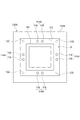
下型110は、水平方向に延在しており、鉛直方向に窪んだ矩形状のキャビティ112を有する。キャビティ112の寸法は、一例として、160mm×160mm×14mm(深さ)である。キャビティ112の内部には、インサート物として電極積層体60が配置される。このとき、電極積層体60は、その積層方向(すなわち、積層体30の積層方向)が鉛直方向と実質的に平行となるように配置される。電極積層体60の寸法は、一例として、150mm×150mm×10mm(高さ)である。キャビティ112は、電極積層体60が配置されたときに、電極積層体60の周囲には均一幅(たとえば5mm幅)の矩形環状の空隙Gが形成される寸法に設計されている。また、キャビティ112の深さは、図2に示したように電極積層体60の周縁部分が第2樹脂部54によって積層方向D1から覆われるように、電極積層体60の高さより所定長さだけ深く設計されている。また、下型110のキャビティ112の底面であって、矩形環状の空隙Gに対応する領域に、4つのセンサ部114が設けられている。本実施形態において、各センサ部114は、一つのセンサで構成されている。センサ部114に用いられるセンサは、空隙G内を流れる樹脂54aの到来を検出するセンサであり、本実施形態では赤外線検出式のフローフロントセンサが採用される。
The
上型120は、下型110と対向するように水平方向に延在しており、下型110に重ね合わされると下型110のキャビティ112を覆う。下型110に対向する上型120の対向面120aには、射出器140から射出された樹脂54aをキャビティ112に注入するためのゲート(注入口)122が4つ設けられている。
The
射出器140は、枠体50の第2樹脂部54となるべき樹脂54aを金型130内に射出する。射出器140のノズルから射出された樹脂54aは、図示しないランナを通って上型120のゲート122まで送られる。射出器140のヘッド部142は、たとえばスクリューやプランジャによって鉛直方向に沿って進退する部分である。ヘッド部142の移動により、射出器140から射出される樹脂54aの射出量や射出圧を調整することができる。
The
コントローラ(制御部)150は、射出器140を制御する部分である。コントローラ150は、特に、射出器140のヘッド部142の移動を制御するとともに、VP切替えをおこなう。すなわち、コントローラ150は、所定のタイミングで、射出器140の射出を速度優先の制御(一次圧)から補圧制御(二次圧)に切り替える。コントローラ150は、下型110に設けられたセンサ部114の検出結果がフィードバック入力されるように構成されている。
The controller (control unit) 150 is a part that controls the
ここで、下型110に設けられた4つのセンサ部114と、上型120に設けられたゲート122との位置関係について、図5を参照しつつ説明する。
Here, the positional relationship between the four
図5に示すように、本実施形態では、キャビティ112に電極積層体60が配置されたときに、電極積層体60の周囲には、積層方向から見て矩形環状の空隙Gが形成される。空隙Gの形状は、より詳しくは正方形の環状であり、空隙Gの四辺に対応する部分の長さが等しい。下型110に設けられた4つのセンサ部114は、空隙Gの四辺の各中点に対応する位置にそれぞれ配置されている。また、上型120に設けられた4つのゲート122は、空隙Gの四隅に対応する位置にそれぞれ配置されている。各ゲート122から空隙G内に注入された樹脂54aは、空隙Gの四隅をそれぞれと起点として空隙G内を辺に沿って流動する。本実施形態では、各ゲート122の開口寸法が同一であり、また、各ゲート122から注入される単位時間当たりの樹脂量が同一であり、さらに、各ゲート122から鉛直方向に沿って下向きに樹脂54aが空隙G内に注入されるため、図5に示すように、各辺に沿って隣り合うゲート122から注入された樹脂同士は当該辺の中点において合流する。換言すると、空隙Gを流れる樹脂同士が合流する位置に、センサ部114が配置されている。
As shown in FIG. 5, in the present embodiment, when the
センサ部114は、樹脂54aの到来を検出するセンサであるため、上記位置に配置することで、空隙Gを流れる樹脂同士が合流するタイミング(または、合流直前のタイミング)を検知することができる。
Since the
続いて、図4に示した製造装置を用いて蓄電モジュール12を作製する手順について、図6を参照しつつ説明する。
Subsequently, a procedure for manufacturing the
蓄電モジュール12を作製する際には、まず、電極積層体60を下型110のキャビティ112内に配置するとともに、所定のガイドピンに沿って下型110に上型120を重ね合わせることで、電極積層体60を金型130内に配置する。(図6のステップS1)
次に、第2樹脂部となるべき樹脂54aの注入を開始する。具体的には、コントローラ150により射出器140を制御して、上型120の各ゲート122からキャビティ112内へ樹脂54aを注入する。この時点では、コントローラ150は、速度優先の一次圧で射出器140の射出を制御する。(図6のステップS2)
そして、ゲート122から空隙Gに流入した樹脂54aが空隙Gの各辺に沿って流れて、樹脂54aがセンサ部114まで到来すると、樹脂54aの到来がセンサ部114によって検出される。(図6のステップS3)
すると、センサ部114の検出結果がコントローラ150に入力されて、それに応じてコントローラ150が射出器140を制御する。(図6のステップS4)より詳しくは、センサ部114から検出結果が入力されると、コントローラ150は、射出器140の射出(すなわち、金型130への樹脂注入)を速度優先制御から保圧制御に切り替える。
When manufacturing the
Next, the injection of the
Then, when the
Then, the detection result of the
射出器140の保圧制御への切替え(VP切替え)のタイミングは、枠体50の第2樹脂部54の形状精度に顕著に影響する。たとえば、コントローラ150による保圧制御への切り替えタイミングが早い場合には、電極積層体60の周囲の空隙Gに樹脂54aが十分に充填されず、その結果、樹脂54aの合流箇所付近に相当する第2樹脂部54の厚さが薄くなってしまう。それにより、第2樹脂部54における十分な気密性や強度を確保することが難しくなる。一方、コントローラ150による保圧制御への切り替えタイミングが遅い場合には、電極積層体60の周囲の空隙Gに充填された樹脂54aが、電極積層体60の第1樹脂部52を比較的高い圧力で外縁側から押圧することとなり、その結果、電極積層体60の外形が顕著に変形する。特に、本実施形態における第1樹脂部52は、薄膜状であり軟弱であるため、変形しやすい。
The timing of switching the
つまり、射出器140の保圧制御への切替えが適切なタイミングであれば、枠体50の変形が抑制されて、枠体50の形状精度の向上を図ることができる。しかしながら、電極積層体60には公差等の個体差が生じやすく、特に、第1樹脂部52の寸法公差や積層ズレが生じやすいため、電極積層体60ごとに適切な保圧制御への切替えタイミングは異なり得る。
That is, if the switching of the
そこで、上述した実施形態においては、電極積層体60が収容された金型130内に樹脂54aが注入されて、電極積層体60の周囲の空隙G内を流れる樹脂54aをセンサ部114が検出したときに、コントローラ150が射出器140のVP切替え制御をおこなっている。このようにセンサ部114による樹脂54aの検出に応じた射出器140の制御をおこなうことで、高い形状精度を有する枠体50を得ることができる。
Therefore, in the above-described embodiment, the
なお、センサ部114は、必ずしも樹脂同士が合流する合流箇所に配置する必要はなく、合流箇所から離れた箇所に配置して樹脂同士の合流タイミングを検出してもよい。たとえば、合流箇所から樹脂54aの上流側にわずかにずらした位置にセンサ部114を配置することで、樹脂同士が合流する前のタイミング(たとえば、合流直前のタイミング)を検知することができ、射出条件によっては、そのタイミングで射出器140を保圧制御へ切替えたほうが好ましい場合もあり得る。
The
なお、センサ部114には、フローフロントセンサ以外に、圧力センサや温度センサを採用することもできる。たとえば、圧力センサでは、樹脂の到来前は圧力ゼロの状態であり樹脂が到来すると圧力が高くなることから、所定の閾値や変化割合に基づいて樹脂の到来を検知することができる。また、温度センサでは、高温の樹脂(たとえば、250℃)が到来すると検出温度が上昇することから、所定の閾値や変化割合に基づいて樹脂の到来を検知することができる。
In addition to the flow front sensor, a pressure sensor or a temperature sensor can also be used for the
また、センサ部114は、必ずしも複数設ける必要はなく、少なくとも1つ設ければよい。センサ部114を複数設けた場合であって、各センサ部114の検知タイミングが異なる場合には、最も早く検知したセンサ部114の検知タイミングを利用してもよく、または、最も早く検知したセンサ部114以外の2番目以降の所定のセンサ部114の検知タイミングを利用してもよい。
Further, it is not always necessary to provide a plurality of
さらに、センサ部114は、図7に示すような一対のセンサ115、116を有するセンサ部114Aに適宜変更することができる。一対のセンサ115、116は、積層方向から見て電極積層体60の周回方向(すなわち、各辺に沿う方向)に離間しており、樹脂同士の合流箇所を挟むように配置されている。この場合、一対のセンサ115、116それぞれにおいて樹脂54aの到来が検知される。センサ部114Aによれば、いずれか一方のセンサ115、116の検知タイミングに応じてコントローラ150が射出器140の保圧制御への切替えをおこなうことができる。たとえば、より早く樹脂54aの到来を検知したほうのセンサ115、116の検知タイミングがコントローラ150に入力される。また、センサ部114Aによれば、両方のセンサ115、116の検知タイミングが所定時間以上離れている場合には、不具合(樹脂注入の不具合やセンサ部自体の故障等)を検出することができる。そのため、センサ部114Aによれば樹脂注入の信頼性向上が図られる。
Further, the
センサ部114、114Aは、必ずしも下型110のキャビティ112の底面に設ける必要はなく、キャビティ112の側面に設けたり上型120に設けたりすることもできる。
The
なお、センサ部114の位置だけでなく、上型120のゲート122の位置についても、適宜変更することができる。
Not only the position of the
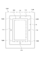
図8に示すように、電極積層体60Bが積層方向から見て長方形状であり、かつ、電極積層体60Bの周囲に形成された空隙Gが積層方向から見て長方形環状である場合には、空隙の四隅から長辺側にずらした位置にゲート122Bを配置し得る。この場合、互いに隣り合うゲート122B間の空隙Gに沿った離間長さ(道のり)を同じすることで、空隙Gの四辺の各中点において樹脂54aが合流するため、空隙Gの四辺の各中点に対応する位置に4つのセンサ部114を配置し得る。
As shown in FIG. 8, when the electrode laminated
また、上記実施形態又は変形例では、蓄電装置10がニッケル水素二次電池の例を挙げて説明したが、蓄電装置10はリチウムイオン二次電池であってもよい。この場合、正極活物質は、例えば複合酸化物、金属リチウム、硫黄等である。負極活物質は、例えば黒鉛、高配向性グラファイト、メソカーボンマイクロビーズ、ハードカーボン、ソフトカーボン等のカーボン、リチウム、ナトリウム等のアルカリ金属、金属化合物、SiOx(0.5≦x≦1.5)等の金属酸化物、ホウ素添加炭素等である。
Further, in the above-described embodiment or modified example, the
12…蓄電モジュール、30…積層体、32…バイポーラ電極、34…電極板、34a…縁部、36…正極、38…負極、50…枠体、52…第1樹脂部、54…第2樹脂部、54a…樹脂、60、60B…電極積層体、100…製造装置、110、110A…上型、112…キャビティ、114、114A…センサ部、120…下型、122、122B…ゲート、130、130A、130B…金型、140…射出器、150…コントローラ、G…空隙、V…内部空間。 12 ... Power storage module, 30 ... Laminate, 32 ... Bipolar electrode, 34 ... Electrode plate, 34a ... Edge, 36 ... Positive electrode, 38 ... Negative, 50 ... Frame, 52 ... First resin part, 54 ... Second resin Part, 54a ... Resin, 60, 60B ... Electrode laminate, 100 ... Manufacturing equipment, 110, 110A ... Upper mold, 112 ... Cavity, 114, 114A ... Sensor part, 120 ... Lower mold, 122, 122B ... Gate, 130, 130A, 130B ... mold, 140 ... injector, 150 ... controller, G ... void, V ... internal space.
Claims (6)
前記複数のバイポーラ電極の各電極板の縁部を保持する複数の第1樹脂部と、前記積層体の積層方向から見て前記複数の第1樹脂部の周囲に設けられた筒状の第2樹脂部とを含む枠体と
を備える蓄電モジュールを作製する蓄電モジュールの製造装置であって、
前記第1樹脂部が設けられた前記バイポーラ電極を複数重ねた電極積層体が収容され、かつ、前記電極積層体が収容されたときに前記積層方向から見て前記電極積層体の周囲に空隙が形成されるキャビティと、前記キャビティの前記空隙に前記第2樹脂部となるべき樹脂を注入する注入口とを有する金型と、
前記樹脂を前記金型内に前記注入口を介して注入する射出器と、
前記積層方向から見て前記電極積層体の周囲であって前記注入口とは異なる箇所における前記金型に配置され、前記空隙内を流れてくる前記樹脂の到達を検知するセンサ部と、
前記射出器の樹脂注入を制御するとともに、前記センサ部が前記樹脂の到達を検知したタイミングに応じて、前記射出器の樹脂注入の保圧制御を始める制御部と
を備える、蓄電モジュールの製造装置。 A laminate in which a plurality of bipolar electrodes including an electrode plate, a positive electrode provided on one surface of the electrode plate, and a negative electrode provided on the other surface of the electrode plate are laminated.
A plurality of first resin portions holding the edges of the respective electrode plates of the plurality of bipolar electrodes, and a tubular second resin portion provided around the plurality of first resin portions when viewed from the stacking direction of the laminate. A device for manufacturing a power storage module that manufactures a power storage module including a frame including a resin portion.
An electrode laminate in which a plurality of the bipolar electrodes provided with the first resin portion are stacked is accommodated, and when the electrode laminate is accommodated, voids are formed around the electrode laminate when viewed from the stacking direction. a cavity formed, the mold having an inlet for injecting a pre-Symbol resin to the second resin portion to the gap of the cavity,
An injection device that injects the resin into the mold through the injection port, and
A sensor unit that is arranged in the mold at a position different from the injection port around the electrode laminate when viewed from the stacking direction and detects the arrival of the resin flowing in the voids.
A power storage module manufacturing apparatus including a control unit that controls resin injection of the injector and starts holding pressure control of resin injection of the injector according to the timing when the sensor unit detects the arrival of the resin. ..
前記金型が前記注入口を複数有し、前記電極積層体の周囲を流れる前記樹脂同士が合流する複数の箇所のうちの少なくとも一部に前記センサ部がそれぞれ配置されており、The mold has a plurality of injection ports, and the sensor unit is arranged at least at least a part of a plurality of locations where the resins flowing around the electrode laminate meet.
前記複数の注入口が、前記積層方向から見て前記電極積層体の周回方向に関して等間隔に離間している、請求項1または2に記載の蓄電モジュールの製造装置。The apparatus for manufacturing a power storage module according to claim 1 or 2, wherein the plurality of injection ports are spaced apart at equal intervals with respect to the circumferential direction of the electrode laminate when viewed from the stacking direction.
前記金型に、前記矩形環状の空隙の四辺のそれぞれに4つのセンサ部が配置されている、請求項1〜3のいずれか一項に記載の蓄電モジュールの製造装置。 The electrode laminate is rectangular when viewed from the stacking direction, and the voids formed around the electrode laminate are rectangular annular when viewed from the stacking direction .
The device for manufacturing a power storage module according to any one of claims 1 to 3, wherein four sensor units are arranged on each of the four sides of the rectangular annular gap in the mold.
前記複数のバイポーラ電極の各電極板の縁部を保持する複数の第1樹脂部と、前記積層体の積層方向から見て前記複数の第1樹脂部の周囲に設けられた筒状の第2樹脂部とを含む枠体と
を備える蓄電モジュールを作製する蓄電モジュールの製造方法であって、
前記第1樹脂部が設けられた前記バイポーラ電極を複数重ねた電極積層体を金型のキャビティ内に収容して、前記積層方向から見て前記電極積層体の周囲に空隙を形成する工程と、
前記第2樹脂部となるべき樹脂を、前記金型に設けられた注入口を介して、制御部によって樹脂注入が制御されている射出器から前記キャビティの前記空隙に注入する工程と、
前記積層方向から見て前記電極積層体の周囲であって前記注入口とは異なる箇所における前記金型に配置されたセンサで、前記空隙内を流れてくる前記樹脂の到達を検知する工程と、
前記センサが前記樹脂の到達を検知したタイミングに応じて、前記制御部が前記射出器の樹脂注入の保圧制御を始める工程と
を含む、蓄電モジュールの製造方法。 A laminate in which a plurality of bipolar electrodes including an electrode plate, a positive electrode provided on one surface of the electrode plate, and a negative electrode provided on the other surface of the electrode plate are laminated.
A plurality of first resin portions holding the edges of the respective electrode plates of the plurality of bipolar electrodes, and a tubular second resin portion provided around the plurality of first resin portions when viewed from the stacking direction of the laminate. A method for manufacturing a power storage module for manufacturing a power storage module including a frame including a resin portion.
A step of accommodating an electrode laminate in which a plurality of the bipolar electrodes provided with the first resin portion are stacked in a cavity of a mold to form a void around the electrode laminate when viewed from the stacking direction.
The resin to be the pre-Symbol second resin part, through the inlet provided in the mold, a step of injecting from the injector to the resin injection is controlled by the gap of the cavity by the control unit,
A step of detecting the arrival of the resin flowing in the void with a sensor arranged in the mold at a position different from the injection port around the electrode laminate when viewed from the stacking direction.
Depending on the timing at which the sensor detects the arrival of the resin, wherein the control unit includes a step of starting the control holding pressure of the resin injected in the injection device, a manufacturing method of the power storage module.
Priority Applications (1)
| Application Number | Priority Date | Filing Date | Title |
|---|---|---|---|
| JP2017108032A JP6787254B2 (en) | 2017-05-31 | 2017-05-31 | Power storage module manufacturing equipment and manufacturing method |
Applications Claiming Priority (1)
| Application Number | Priority Date | Filing Date | Title |
|---|---|---|---|
| JP2017108032A JP6787254B2 (en) | 2017-05-31 | 2017-05-31 | Power storage module manufacturing equipment and manufacturing method |
Publications (3)
| Publication Number | Publication Date |
|---|---|
| JP2018206533A JP2018206533A (en) | 2018-12-27 |
| JP2018206533A5 JP2018206533A5 (en) | 2019-12-05 |
| JP6787254B2 true JP6787254B2 (en) | 2020-11-18 |
Family
ID=64958094
Family Applications (1)
| Application Number | Title | Priority Date | Filing Date |
|---|---|---|---|
| JP2017108032A Active JP6787254B2 (en) | 2017-05-31 | 2017-05-31 | Power storage module manufacturing equipment and manufacturing method |
Country Status (1)
| Country | Link |
|---|---|
| JP (1) | JP6787254B2 (en) |
Families Citing this family (3)
| Publication number | Priority date | Publication date | Assignee | Title |
|---|---|---|---|---|
| JP7319060B2 (en) * | 2019-02-27 | 2023-08-01 | 現代自動車株式会社 | All-solid battery |
| KR20210040719A (en) * | 2019-10-04 | 2021-04-14 | 주식회사 엘지화학 | Battery module, battery pack comprising the battery module and vehicle comprising the battery pack |
| KR20210143565A (en) * | 2020-05-20 | 2021-11-29 | 주식회사 엘지에너지솔루션 | System and method for ultrasonic inspection |
Family Cites Families (6)
| Publication number | Priority date | Publication date | Assignee | Title |
|---|---|---|---|---|
| FI77543C (en) * | 1985-12-19 | 1989-03-10 | Neste Oy | ACKUMULATOR. |
| CA2118866A1 (en) * | 1993-06-21 | 1994-12-22 | Clarence A. Meadows | Bipolar battery housing and method |
| JP2001219440A (en) * | 2000-02-09 | 2001-08-14 | Sony Disc Technology Inc | Multi-cavity molding apparatus and its molding method |
| DE102004031546A1 (en) * | 2004-06-29 | 2006-02-09 | Priamus System Technologies Ag | Method for filling at least one cavity |
| JP2006224499A (en) * | 2005-02-18 | 2006-08-31 | Hirotec Corp | Injection molding machine and injection molding method |
| JP5484426B2 (en) * | 2011-10-26 | 2014-05-07 | 豊田合成株式会社 | Battery module and battery unit |
-
2017
- 2017-05-31 JP JP2017108032A patent/JP6787254B2/en active Active
Also Published As
| Publication number | Publication date |
|---|---|
| JP2018206533A (en) | 2018-12-27 |
Similar Documents
| Publication | Publication Date | Title |
|---|---|---|
| US11276903B2 (en) | Electricity storage device and method for manufacturing electricity storage device | |
| JP6953840B2 (en) | Power storage device and its manufacturing method | |
| JP6787254B2 (en) | Power storage module manufacturing equipment and manufacturing method | |
| US11955593B2 (en) | Power storage module and method for manufacturing power storage module | |
| JP6805844B2 (en) | Manufacturing method of power storage module | |
| WO2018116725A1 (en) | Electricity storage module and method for manufacturing electricity storage module | |
| JP2019012653A (en) | Power storage device and manufacturing method for the same | |
| CN111194499B (en) | Power storage module | |
| JP7102911B2 (en) | Manufacturing method of power storage module | |
| JP7056102B2 (en) | Manufacturing method of power storage module and power storage module | |
| JP7103272B2 (en) | Power storage module and its manufacturing method | |
| JP7059793B2 (en) | Manufacturing method of power storage module and jig for manufacturing power storage module | |
| JP7027996B2 (en) | Mold | |
| JP2021044079A (en) | Power storage module, and manufacturing method of power storage module | |
| JP2020119669A (en) | Manufacturing method of power storage module | |
| JP6965730B2 (en) | Manufacturing method of power storage module | |
| JP2019200962A (en) | Manufacturing method of power storage module and power storage module | |
| JP7103055B2 (en) | Power storage module and manufacturing method of power storage module | |
| JP7095630B2 (en) | Power storage module manufacturing equipment and power storage module manufacturing method | |
| JP7196693B2 (en) | Electric storage module manufacturing method and electric storage module manufacturing apparatus | |
| JP7110875B2 (en) | Electric storage module manufacturing method and electric storage module manufacturing apparatus | |
| JP7188062B2 (en) | Storage module manufacturing apparatus and manufacturing method | |
| JP7070284B2 (en) | Power storage module and manufacturing method of power storage module | |
| JP6965731B2 (en) | Power storage module and manufacturing method of power storage module | |
| JP2020140862A (en) | Power storage module manufacturing apparatus and manufacturing method |
Legal Events
| Date | Code | Title | Description |
|---|---|---|---|
| A521 | Written amendment |
Free format text: JAPANESE INTERMEDIATE CODE: A523 Effective date: 20191028 |
|
| A621 | Written request for application examination |
Free format text: JAPANESE INTERMEDIATE CODE: A621 Effective date: 20191028 |
|
| A977 | Report on retrieval |
Free format text: JAPANESE INTERMEDIATE CODE: A971007 Effective date: 20200916 |
|
| TRDD | Decision of grant or rejection written | ||
| A01 | Written decision to grant a patent or to grant a registration (utility model) |
Free format text: JAPANESE INTERMEDIATE CODE: A01 Effective date: 20200929 |
|
| A61 | First payment of annual fees (during grant procedure) |
Free format text: JAPANESE INTERMEDIATE CODE: A61 Effective date: 20201012 |
|
| R151 | Written notification of patent or utility model registration |
Ref document number: 6787254 Country of ref document: JP Free format text: JAPANESE INTERMEDIATE CODE: R151 |