JP6774792B2 - Infrared device - Google Patents
Infrared device Download PDFInfo
- Publication number
- JP6774792B2 JP6774792B2 JP2016123281A JP2016123281A JP6774792B2 JP 6774792 B2 JP6774792 B2 JP 6774792B2 JP 2016123281 A JP2016123281 A JP 2016123281A JP 2016123281 A JP2016123281 A JP 2016123281A JP 6774792 B2 JP6774792 B2 JP 6774792B2
- Authority
- JP
- Japan
- Prior art keywords
- layer
- photoelectric conversion
- infrared
- conversion unit
- infrared device
- Prior art date
- Legal status (The legal status is an assumption and is not a legal conclusion. Google has not performed a legal analysis and makes no representation as to the accuracy of the status listed.)
- Active
Links
Images


Landscapes
- Led Devices (AREA)
- Light Receiving Elements (AREA)
- Photometry And Measurement Of Optical Pulse Characteristics (AREA)
- Optical Integrated Circuits (AREA)
Description
本発明は、赤外線を受光および発光の少なくとも一方を行う赤外線デバイスに関する。 The present invention relates to an infrared device that receives and emits infrared light at least.
赤外線デバイスのうち、受光した赤外線に応じた信号を出力する赤外線受光デバイスは、光通信分野、省エネルギー分野あるいはガスセンサ等の環境分野において用いられるようになってきている。 Among infrared devices, infrared light receiving devices that output signals corresponding to received infrared rays have come to be used in the fields of optical communication, energy saving, and environmental fields such as gas sensors.
また、赤外線デバイスのうち、赤外線を発光する赤外線発光デバイスは、注入された電流によって発光する発光ダイオードの形態での開発が進められている。 Further, among infrared devices, an infrared light emitting device that emits infrared rays is being developed in the form of a light emitting diode that emits light by an injected current.
従来の赤外線デバイスでは、複合基板に対して垂直方向(便宜的に縦方向とも称する)から入射される赤外線の制御や、複合基板に対して縦方向に出射する赤外線の制御に着目して開発が進められている。しかし、従来の赤外線デバイスでは、複合基板に対して平面方向(便宜的に横方向とも称する)から入射する赤外線や、複合基板に対して横方向に出射する赤外線の制御はあまり着目されていないのが実情である。 Conventional infrared devices have been developed by focusing on the control of infrared rays that are incident on the composite substrate in the vertical direction (also referred to as the vertical direction for convenience) and the control of infrared rays that are emitted in the vertical direction of the composite substrate. It is being advanced. However, in the conventional infrared device, the control of infrared rays incident on the composite substrate from the plane direction (also referred to as the lateral direction for convenience) and infrared rays emitted from the composite substrate in the lateral direction has not received much attention. Is the reality.
例えば特許文献1には、視野角を制御するための周辺部材として開口部を有するコールドシールドが開示されているが、横方向から到来する赤外線を受光部に入射させることは困難である。特許文献2には、発光した赤外線のうち、本来意図した出射方向とは逆の方向に発光した赤外線を意図した出射方向に出射させるための周辺部材として反射層を設ける技術が開示されている。しかし、特許文献2に開示された技術では、横方向に広がっていく赤外線には着目されていない。特許文献3には、赤外線を広い面積において均一に照射するために、周辺部材として拡散板を設ける技術が開示されている。この技術は、縦方向に出射した赤外線を横方向に広げるための技術であるが、周辺部材を必要とするため、赤外線デバイスの大型化が避けられない。また、特許文献3に開示された技術では、もともと横方向に出射した赤外線には着目されていない。
For example, Patent Document 1 discloses a cold shield having an opening as a peripheral member for controlling a viewing angle, but it is difficult to inject infrared rays arriving from the lateral direction into a light receiving portion.
本発明は、周辺部材を用いることなく複合基板に対して平面方向からの赤外線の入射および複合基板に対して平面方向への赤外線の出射の少なくとも一方を制御することが可能な赤外線デバイスを提供することを目的とする。 The present invention provides an infrared device capable of controlling at least one of the incident of infrared rays from a plane direction on a composite substrate and the emission of infrared rays in a plane direction to a composite substrate without using peripheral members. The purpose is.
本発明の一態様による赤外線デバイスは、第1の材料で形成されて厚みが0.1μm以上100μm以下の第1の層、および波長5μmの赤外線に対する屈折率が第1の材料よりも小さい第2の材料で形成された第2の層を有する複合基板と、前記第1の層上に形成されて半導体積層部を有する少なくとも1つの光電変換部と、を備え、前記第1の層の一部は、前記光電変換部が形成されている側の前記複合基板の表面において露出していることを特徴とする。 The infrared device according to one aspect of the present invention has a first layer formed of a first material and having a thickness of 0.1 μm or more and 100 μm or less, and a second layer having a refractive index with respect to infrared rays having a wavelength of 5 μm smaller than that of the first material. A composite substrate having a second layer formed of the above material, and at least one photoelectric conversion unit formed on the first layer and having a semiconductor laminated portion, and a part of the first layer. Is exposed on the surface of the composite substrate on the side where the photoelectric conversion portion is formed .
本発明の一態様による赤外線デバイスによれば、周辺部材を用いることなく複合基板に対して平面方向からの赤外線の入射および複合基板に対して平面方向への赤外線の出射を制御することが可能になる。 According to the infrared device according to one aspect of the present invention, it is possible to control the incident of infrared rays from the plane direction on the composite substrate and the emission of infrared rays in the plane direction to the composite substrate without using peripheral members. Become.
以下、実施形態を通じて本発明を説明するが、以下の実施形態は特許請求の範囲に係る発明を限定するものではない。また、実施形態の中で説明されている特徴の組み合わせの全てが本発明の解決手段に必須であるとは限らない。 Hereinafter, the present invention will be described through embodiments, but the following embodiments do not limit the invention according to the claims. Also, not all combinations of features described in the embodiments are essential to the solution of the present invention.
<赤外線デバイス>
本発明の実施形態による赤外線デバイスは、第1の材料で形成されて厚みが0.1μm以上100μm以下の第1の層、および波長5μmの赤外線に対する屈折率が第1の材料よりも小さい第2の材料で形成された第2の層を有する複合基板と、第1の層上に形成された半導体積層部を有する少なくとも1つの光電変換部と、を備える。
<Infrared device>
The infrared device according to the embodiment of the present invention has a first layer formed of a first material and having a thickness of 0.1 μm or more and 100 μm or less, and a second layer having a refractive index with respect to infrared rays having a wavelength of 5 μm smaller than that of the first material. A composite substrate having a second layer formed of the above material, and at least one photoelectric conversion unit having a semiconductor laminated portion formed on the first layer.
本実施形態による赤外線デバイスは、第1の材料で形成されて厚みが0.1μm以上100μm以下の第1の層、および波長5μmの赤外線に対する屈折率が第1の材料よりも小さい第2の材料で形成された第2の層を有する複合基板を用いることにより、複合基板に対して平面方向から入射した赤外線を効率的に光電変換部に到達させることが可能になる。また、本実施形態による赤外線デバイスは、このような複合基板を用いることにより、光電変換部から複合基板に対して平面方向に出射した赤外線を効率的に外部に出射することが可能になる。 The infrared device according to the present embodiment is a first layer formed of a first material and having a thickness of 0.1 μm or more and 100 μm or less, and a second material having a refractive index with respect to infrared rays having a wavelength of 5 μm smaller than that of the first material. By using the composite substrate having the second layer formed of the above, it is possible to efficiently make the infrared rays incident on the composite substrate from the plane direction reach the photoelectric conversion unit. Further, in the infrared device according to the present embodiment, by using such a composite substrate, it is possible to efficiently emit infrared rays emitted from the photoelectric conversion unit in the plane direction to the composite substrate to the outside.
ここで、「複合基板に対して平面方向」とは、複合基板の平面を基準にして45度以下の角度の範囲の方向を意味する。 Here, the "planar direction with respect to the composite substrate" means a direction in an angle range of 45 degrees or less with respect to the plane of the composite substrate.
また、屈折率は、各々の大小関係が定まれば特に制限されず、実際に5μmの赤外線を適当な角度で透過させたときに進行する光線の挙動から求めてもよいし、各層の材料の屈折率の絶対値から求めてもよい。 Further, the refractive index is not particularly limited as long as the magnitude relationship of each is determined, and may be obtained from the behavior of light rays traveling when infrared rays of 5 μm are actually transmitted at an appropriate angle, or the material of each layer may be obtained. It may be obtained from the absolute value of the refractive index.
<複合基板>
複合基板は、第1の材料で形成されて厚みが0.1μm以上100μm以下の第1の層と、波長5μmの赤外線に対する屈折率が第1の材料よりも小さい第2の材料で形成された第2の層とを有していれば特に制限されない。第1の層の厚みが0.1μm以上100μm以下であることにより、光電変換部へ入射した赤外線や、光電変換部から放出された赤外線の吸収が抑えられ、赤外線デバイスの性能向上が実現できる。赤外線の吸収を抑制することや、横方向に進行する赤外線を制御する観点から、光電変換部が形成される領域と光電変換部が形成されていない領域で、第1の層の厚みが異なっていても良い。
<Composite board>
The composite substrate was formed of a first layer formed of the first material and having a thickness of 0.1 μm or more and 100 μm or less, and a second material having a refractive index of 5 μm for infrared rays smaller than that of the first material. It is not particularly limited as long as it has a second layer. When the thickness of the first layer is 0.1 μm or more and 100 μm or less, the absorption of infrared rays incident on the photoelectric conversion unit and infrared rays emitted from the photoelectric conversion unit can be suppressed, and the performance of the infrared device can be improved. From the viewpoint of suppressing the absorption of infrared rays and controlling the infrared rays traveling in the lateral direction, the thickness of the first layer is different between the region where the photoelectric conversion portion is formed and the region where the photoelectric conversion portion is not formed. You may.
第1の層は光電変換部と接する層である。詳細は後述するが、光電変換部は、分子線エピタキシー(Molecular Beam Epitaxy:MBE)法、有機金属気相成長(Metalorganig Chemical Vapor Deposition:MOCVD)法、または、接着法を用いて形成することが出来る。光電変換部と第1の層との界面を高い品質にする観点から、MBE法またはMOCVD法は好ましい場合がある。光電変換部をMBE法またはMOCVD法で形成する場合、光電変換部の結晶性を向上させる観点から、第1の材料は単結晶であってもよく、具体的にはSi単結晶(屈折率約3.4)またはGaAs単結晶(屈折率約3.3)であってもよい。 The first layer is a layer in contact with the photoelectric conversion unit. Although the details will be described later, the photoelectric conversion unit can be formed by using a molecular beam epitaxy (MBE) method, a metalorganic chemical vapor deposition (MOCVD) method, or an adhesive method. .. The MBE method or the MOCVD method may be preferable from the viewpoint of improving the quality of the interface between the photoelectric conversion unit and the first layer. When the photoelectric conversion part is formed by the MBE method or the MOCVD method, the first material may be a single crystal from the viewpoint of improving the crystallinity of the photoelectric conversion part, and specifically, a Si single crystal (refractive coefficient: about). It may be 3.4) or a GaAs single crystal (refractive coefficient of about 3.3).
第2の材料は、第1の材料よりも屈折率が小さい材料である。第2の層の具体的な形成材料としては、SiO2(屈折率は約1.4)やAl2O3(屈折率は約1.7)などが挙げられる。複数の光電変換部を有する赤外線デバイスの場合、第1の層をエッチングすることで複合基板側の各々の光電変換部の電気的絶縁性を向上させる観点から、第2の層は絶縁性であってもよい。 The second material is a material having a lower refractive index than the first material. Specific examples of the material for forming the second layer include SiO 2 (refractive index of about 1.4) and Al 2 O 3 (refractive index of about 1.7). In the case of an infrared device having a plurality of photoelectric conversion units, the second layer is insulating from the viewpoint of improving the electrical insulation of each photoelectric conversion unit on the composite substrate side by etching the first layer. You may.
特に制限はされないが、電気的絶縁性及び光学的な透過率を確保する観点から、第1の材料は、抵抗率が10kΩ・cm以上1GΩ・cm以下の絶縁材料であってもよい。複合基板に対して平行方向の赤外線を制御する観点から、光電変換部が形成されている側の複合基板の表面において第1の層の一部が露出していてもよい。すなわち、複合基板に対して平行方向の赤外線を制御する観点から、複合基板の第1の層の表面のうち、光電変換部が形成されていない表面の少なくとも一部が固体で覆われていなくてもよい。 Although not particularly limited, the first material may be an insulating material having a resistivity of 10 kΩ · cm or more and 1 GΩ · cm or less from the viewpoint of ensuring electrical insulation and optical transmittance. From the viewpoint of controlling infrared rays in the direction parallel to the composite substrate, a part of the first layer may be exposed on the surface of the composite substrate on the side where the photoelectric conversion unit is formed. That is, from the viewpoint of controlling infrared rays in the direction parallel to the composite substrate, at least a part of the surface of the first layer of the composite substrate on which the photoelectric conversion portion is not formed is not covered with a solid. May be good.
複合基板は、必要に応じて第1の層が存在しない側の面上に第3の材料で形成された第3の層をさらに有していてもよい。この場合、第3の層の厚みは、複合基板の強度を保つ観点から、50μm以上1000μm以下であってもよい。第3の材料としては、Si、ガラスあるいはGaAsなどが挙げられる。第3の材料がSiの場合、大口径のウエハーが一般的に使われるが、加工時のハンドリングの観点から、加工の段階では第3の層の厚みを500μm以上800μm以下としておき、加工工程の途中に、デバイスの最終厚みになるように薄くしても良い。また、加工の段階では第3の層を厚く(例えば800μm)しておき、一部の工程を通ってから、加工の途中で研摩等によって第3の層を薄型化しても良い。 The composite substrate may further have a third layer formed of the third material on the surface on the side where the first layer does not exist, if necessary. In this case, the thickness of the third layer may be 50 μm or more and 1000 μm or less from the viewpoint of maintaining the strength of the composite substrate. Examples of the third material include Si, glass and GaAs. When the third material is Si, a large-diameter wafer is generally used, but from the viewpoint of handling during processing, the thickness of the third layer is set to 500 μm or more and 800 μm or less at the processing stage in the processing process. On the way, it may be thinned to the final thickness of the device. Further, the third layer may be made thicker (for example, 800 μm) at the processing stage, and after passing through some steps, the third layer may be made thinner by polishing or the like during the processing.
第3の層を有さない場合、複合基板の強度を保つ観点から、第1の層の厚みが、第2の層の厚みよりも薄くてもよい。一例としては、第2の層として十分な厚みを有するサファイア(Al2O3)上に第1の層としてシリコンが形成されたSOS(Silicon on sapphire)基板が挙げられる。 When the third layer is not provided, the thickness of the first layer may be thinner than the thickness of the second layer from the viewpoint of maintaining the strength of the composite substrate. One example is an SOS (Silicon on sapphire) substrate in which silicon is formed as a first layer on sapphire (Al 2 O 3 ) having a sufficient thickness as a second layer.
複合基板の他の一例としては、第2の層としての絶縁層(例えばSiO2)の上に第1の層としてシリコンが形成されたSOI(Silicon On Insulator)基板であっても良い。SOI基板の中で、SiO2を絶縁層にした基板もあれば、γアルミナを絶縁層にした基板もある。SiO2を絶縁層にしたSOI基板である場合、大口径が実現され、一般的なLSIの製造に利用でき、高品質な複合基板が実現できる。第1の層は、高品質の結晶性が要求されると共に、前述のように、ターゲット波長帯に於いて、高い透過率を持つ必要がある。また、第3の層を有する場合は、第2の層と第3の層との界面が急峻であると好ましい場合がある。SOI基板の製造方法としては、SIMOX(separation by implantation of oxigen)や貼り合わせ法(例えばsmart cut process)が挙げられる。第3の層を有するSOI基板の場合、第2の層と第3の層との界面を急峻にするため、貼り合わせ法を用いて造られるSOI複合基板であってもよい。 As another example of the composite substrate, an SOI (Silicon On Insulator) substrate in which silicon is formed as a first layer on an insulating layer (for example, SiO 2 ) as a second layer may be used. Among the SOI substrates, there are substrates in which SiO 2 is used as an insulating layer, and there are substrates in which γ-alumina is used as an insulating layer. In the case of an SOI substrate having SiO 2 as an insulating layer, a large diameter can be realized, which can be used for manufacturing a general LSI, and a high-quality composite substrate can be realized. The first layer is required to have high quality crystallinity and, as described above, to have high transmittance in the target wavelength band. Further, when the third layer is provided, it may be preferable that the interface between the second layer and the third layer is steep. Examples of the method for manufacturing an SOI substrate include SIMOX (separation by implantation of oxygen) and a bonding method (for example, smart cut process). In the case of an SOI substrate having a third layer, in order to make the interface between the second layer and the third layer steep, an SOI composite substrate made by using a bonding method may be used.
<光電変換部>
光電変換部は、入射した赤外線に応じた電気信号を出力する又は入射した赤外線に応じた抵抗変化を示す受光部であってもよいし、注入された注入電流によって赤外線を発光する発光部であってもよい。本実施形態の赤外線デバイスは、受光部および発光部の少なくとも一方を備えていれば特に制限されない。発光部で生成される赤外線をモニタリングする観点や、受光部の温度特性を抑制する観点から、受光部および発光部の両方を備えていてもよい。受光部および発光部は、同じ積層構造を有し、且つ、同じ材料で形成されていてもよい。受光部および発光部の両方を備えている場合、発光部で生成される赤外線のモニタリング精度や温度特性の抑制精度を向上させる観点から、材料のうち第1の層に接する受光部および発光部の材料の波長5μmの赤外線に対する屈折率は、第1の材料の屈折率に対する比が0.8以上1.2以下であってよく、0.9以上1.15以下であってもよい。
<Photoelectric conversion unit>
The photoelectric conversion unit may be a light receiving unit that outputs an electric signal corresponding to the incident infrared rays or exhibits a resistance change according to the incident infrared rays, or is a light emitting unit that emits infrared rays by the injected injection current. You may. The infrared device of the present embodiment is not particularly limited as long as it includes at least one of a light receiving unit and a light emitting unit. Both the light receiving unit and the light emitting unit may be provided from the viewpoint of monitoring the infrared rays generated by the light emitting unit and suppressing the temperature characteristics of the light receiving unit. The light receiving part and the light emitting part may have the same laminated structure and may be made of the same material. When both the light receiving unit and the light emitting unit are provided, the light receiving unit and the light emitting unit in contact with the first layer of the material are provided from the viewpoint of improving the monitoring accuracy of infrared rays generated by the light emitting unit and the suppression accuracy of temperature characteristics. The refractive index of the material with respect to infrared rays having a wavelength of 5 μm may be such that the ratio of the first material to the refractive index is 0.8 or more and 1.2 or less, and 0.9 or more and 1.15 or less.
また、複合基板に対して平面方向からの赤外線の入射および複合基板に対して平面方向への赤外線の出射の少なくとも一方を制御する観点から、第1の層に接する光電変換部の層材料の波長5μmの赤外線に対する屈折率が、第1の材料の屈折率よりも大くてもよい場合がある。 Further, from the viewpoint of controlling at least one of the infrared ray incident from the plane direction on the composite substrate and the infrared ray emission from the plane direction to the composite substrate, the wavelength of the layer material of the photoelectric conversion unit in contact with the first layer. In some cases, the refractive index for infrared rays of 5 μm may be higher than the refractive index of the first material.
受光部の種類としては熱型の光電変換部であってもよいし、量子型の光電変換部であってもよい。量子型の光電変換部の一例としては、光起電力型(具体的にはフォトダイオード等)や光導電型(具体的にはフォトコンダクター等)やフォトトランジスター等が挙げられる。異なる型の光電変換部を有していてもよい。また、光電変換部は、感度および発光効率が高められるという観点から、単結晶の半導体材料から形成されていてもよい。光電変換部が半導体材料から形成されている場合、光電変換部の構成として、n型半導体層およびp型半導体層を有する積層部を含むpn接合を有する構成や、n型半導体層およびp型半導体層の間にi型半導体層をさらに含むpin接合を有する構成が挙げられる。光電変換部が半導体材料を有している場合、光電変換部は、III族またはV族の元素から形成されてもよい。具体的な例としては1μmから12μm波長帯の赤外線を吸収または放出する光電変換部であっても良い。具体的な材料としてはInSb(屈折率は約4)、AlGaSb、InAs、InAlSbおよびInAsSbなどが挙げられる。これらの材料を利用した光電変換部は、発光波長帯及び受光波長帯を数μmから十数μmまで設定することができ、非分散型赤外線(Non Dispersive InfraRed:NDIR)方式を使ったガスセンサに応用できる。 The type of the light receiving unit may be a thermal type photoelectric conversion unit or a quantum type photoelectric conversion unit. Examples of the quantum type photoelectric conversion unit include a photovoltaic type (specifically, a photodiode and the like), a photoconducting type (specifically, a photoconductor and the like), a phototransistor and the like. It may have a different type of photoelectric conversion unit. Further, the photoelectric conversion unit may be formed of a single crystal semiconductor material from the viewpoint of increasing sensitivity and luminous efficiency. When the photoelectric conversion unit is formed of a semiconductor material, the photoelectric conversion unit may be configured to have a pn junction including a laminated portion having an n-type semiconductor layer and a p-type semiconductor layer, or an n-type semiconductor layer and a p-type semiconductor. Examples thereof include a configuration having a pin junction including an i-type semiconductor layer between the layers. When the photoelectric conversion unit has a semiconductor material, the photoelectric conversion unit may be formed from a group III or group V element. As a specific example, a photoelectric conversion unit that absorbs or emits infrared rays in the wavelength band of 1 μm to 12 μm may be used. Specific materials include InSb (refractive index is about 4), AlGaSb, InAs, InAlSb, InAsSb and the like. The photoelectric conversion unit using these materials can set the emission wavelength band and the light reception wavelength band from several μm to more than ten μm, and is applied to a gas sensor using a non-dispersive infrared (NDIR) method. it can.
制限はされないが、光電変換部は、単結晶成長法を利用して形成されてから、フォトリソグラフィ工程や酸によるウエットエッチング、または、反応性のドライエッチングを利用して形成することが出来る。 Although not limited, the photoelectric conversion unit can be formed by using a single crystal growth method and then by a photolithography step, wet etching with an acid, or reactive dry etching.
以下、図面を参酌しながら本実施形態に係る赤外線デバイスをより詳細に説明する。 Hereinafter, the infrared device according to the present embodiment will be described in more detail with reference to the drawings.
(第1構成例)
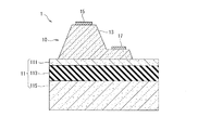
図1は、本実施形態の第1構成例に係る赤外線デバイス1の断面の構成例を示す。
図1に示すように、複合基板11は、第1の層111、第2の層113および第3の層115の多層構造を有している。複合基板11は上述の複合基板に相当し、第1の層111は上述の第1の層に相当し、第2の層113は上述の第2の層に相当し、第3の層115は上述の第3の層に相当する。
(First configuration example)
FIG. 1 shows a configuration example of a cross section of the infrared device 1 according to the first configuration example of the present embodiment.
As shown in FIG. 1, the composite substrate 11 has a multilayer structure of a
赤外線デバイス1は、複合基板11の第1の層111上に形成された光電変換部10を有している。光電変換部10は、段差を有するメサ状の半導体積層部13と、光電変換部10の接続端子として用いられる電極15及び電極17とを有している。電極15および電極17は半導体積層部13に配置されている。電極15は、電極17よりも第1の層111から離れた位置に配置されている。
The infrared device 1 has a
電極15,17を経由して電流を入力したり光起電力を取り出したりすることができる。光電変換部10は、PNやPINフォトダイオード構造を有していても良いし、同一型の半導体で形成されるフォトコンダクター構造を有していても良い。光電変換部10がフォトコンダクター構造を有している場合、光によって起電力が発生しないため、印加バイアスが必要となる。この場合、光導電型(フォトコンダクター)タイプでは、入力電流が複合基板11の表面に対して垂直および斜めの少なくとも一方に流れることとなる。光デバイスの設計によって、光電変換部10は、いずれかまたは両方のフォトコンダクター構造を有しても良い。
A current can be input or a photovoltaic power can be taken out via the
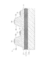
(第2構成例)
図2は、本実施形態の第2構成例に係る赤外線デバイス2の断面の構成例を示す。なお、第1構成例による赤外線デバイス1と同様の作用・機能を奏する構成要素には同一の符号を付して、その説明は省略する。
(Second configuration example)
FIG. 2 shows a configuration example of a cross section of the
図2に示すように、第2構成例による赤外線デバイス2では、光電変換部20として、複合基板11の表面に対して電流が主に水平方向に流れる光導電型の受光部が採用されている。光電変換部20は、複合基板11を構成する第1の層111の表面にほぼ平行に形成された平板状の半導体積層部19を有している。電極15及び電極17は、半導体積層部19の平坦な面上に第1の層111とほぼ平行に配置されている。赤外線デバイス2において、電極15および電極17を通してバイアスを印加すると、入射光強度によって光電変換部20(より具体的には半導体積層部19)の抵抗が変化する。このため、赤外線デバイス2は、このバイアスによる電圧または電流の変化を光電変換信号として取り出すことができる。
As shown in FIG. 2, in the
(第3構成例)
図3は、本実施形態の第3構成例に係る赤外線デバイス3の断面の構成例を示す。なお、第1構成例による赤外線デバイス1と同様の作用・機能を奏する構成要素には同一の符号を付して、その説明は省略する。
(Third configuration example)
FIG. 3 shows a configuration example of a cross section of the infrared device 3 according to the third configuration example of the present embodiment. The components having the same functions and functions as those of the infrared device 1 according to the first configuration example are designated by the same reference numerals, and the description thereof will be omitted.
図3に示すように、第3構成例に係る赤外線デバイス3は、2つの光電変換部30a,30bを備えている。光電変換部30aは、段差を有するメサ形状の半導体積層部13aと、光電変換部30aの接続端子として用いられる電極15a及び電極17aとを有している。電極15aおよび電極17aは半導体積層部13aに配置されている。電極15aは、電極17aよりも第1の層111から離れた位置に配置されている。光電変換部30bは、段差を有するメサ形状の半導体積層部13bと、光電変換部30bの接続端子として用いられる電極15b及び電極17bとを有している。電極15bおよび電極17bは半導体積層部13bに配置されている。電極15bは、電極17bよりも第1の層111から離れた位置に配置されている。電極15a,15bは、上記第1構成例における電極15と同様の作用・機能を奏し、電極17a,17bは、上記第1構成例における電極17と同様の作用・機能を奏する。
As shown in FIG. 3, the infrared device 3 according to the third configuration example includes two
光電変換部30aと光電変換部30bとの間には、エッチング部117が設けられている。エッチング部117を設けることで、光電変換部30aと光電変換部30bとの間の電気的絶縁を向上することができる。そうすることで、光電変換部30aおよび光電変換部30b同士の直列または並列接続が容易となる。また、発光部と受光部の両方と、これらの間に設けられたエッチング部とを備える赤外線デバイスは、エッチング部を有しない場合と比較して、発光部に導入される電流の一部がリーク電流として複合基板を介して受光部に流入してしまうのを大幅に抑制できる。これにより、この赤外線デバイスは、このリーク電流によるノイズが発光部で生じることを防ぐことができる。例えば光電変換部30aが発光部であり、光電変換部30bが受光部である場合、赤外線デバイス3は、電極15aおよび電極17aの一方から導入される電流の一部がリーク電流として複合基板11を介して光電変換部30bに流入するのをエッチング部117によって大幅に抑制できる。これにより、赤外線デバイス3は、このリーク電流によるノイズが光電変換部30aに生じることを防ぐことができる。
An
(第4構成例)
図4は、本実施形態の第4構成例に係る赤外線デバイス4の断面の構成例を示す。なお、第1構成例による赤外線デバイス1と同様の作用・機能を奏する構成要素には同一の符号を付して、その説明は省略する。
(Fourth configuration example)
FIG. 4 shows a configuration example of a cross section of the infrared device 4 according to the fourth configuration example of the present embodiment. The components having the same functions and functions as those of the infrared device 1 according to the first configuration example are designated by the same reference numerals, and the description thereof will be omitted.
図4に示すように、赤外線デバイス4は、材料および組成の少なくとも一方やドーパントが異なる半導体層が積層された光電変換部40を備えている。光電変換部40は、PIN構造の半導体積層部21を有している。半導体積層部21は、段差を有するメサ状に形成されている。半導体積層部21は、複合基板11の第1の層111上に形成されたn層219と、n層219上に形成されたnバリア層217と、nバリア層217上に形成された活性層215と、活性層215上に形成されたpバリア層213と、pバリア層213上に形成されたp層211とを有している。
As shown in FIG. 4, the infrared device 4 includes a
活性層215は、赤外線を吸収または放出する層である。光電変換部40が例えば受光部である場合には、活性層215は赤外線を吸収する層として機能する。一方、光電変換部40が例えば発光部である場合には、活性層215は赤外線を放出する層として機能する。活性層215は、バンドギャップを変えることで、発光波長帯と受光波長帯を変えることができる。一例としては活性層215がInSbで形成されている場合、発光波長帯と受光波長帯のピーク波長は5μm付近となる。
The
nバリア層217及びpバリア層213は、活性層215よりもバンドギャップが大きく設定されても良い。そうすると、光電変換部40が受光部として動作される場合、キャリアの拡散防止効果による高S/N比が実現でき、光電変換部40が発光部として動作される場合、キャリアの閉じこみによる効果によって発光効率が改善できる。また、pバリア層213およびnバリア層217は異なるバンドオフセットを有しても良い。一般的に、pバリア層213およびnバリア層217のバンドオフセットは、半導体積層部21の発光効率(光電変換部40が発光部として動作する場合)や受光効率(光電変換部40が受光部として動作する場合)が最適になるように活性層215の形成材料によって設定される。
The bandgap of the n-
p層211はp型半導体で形成された層である。p層211は、光電変換部40が受光部として動作する場合にはホールの取り出し層として動作する。一方、p層211は、光電変換部40が発光部として動作する場合にはホール注入層として利用される。
The p-
n層219はn型半導体で形成されている。n層219は、光電変換部40が受光部として動作する場合には電子の取り出し層として動作する。一方、n層219は、光電変換部40が発光部として動作する場合には電子注入層として利用される。
The n-
光電変換部40は、半導体積層部21の一部を覆って設けられた絶縁層(パッシベーション層)23を有している。絶縁層23は、光電変換部40の側面、すなわち半導体積層部21の側面の絶縁性を確保する役割を持つ。絶縁層23を形成するために使用できる具体的な材料として、例えば窒化ケイ素、酸化ケイ素およびアルミナなどが挙げられる。
The
光電変換部40は、メタル層25を有している。メタル層25の一部は、p層211上の絶縁層23の一部に形成されてp層211の少なくとも一部を露出するコンタクトホール251に埋め込まれている。これにより、メタル層25はp層211に接続される。また、メタル層25の他の一部は、n層219上の絶縁層23の一部に形成されてn層219の一部を露出するコンタクトホール252に埋め込まれている。これにより、メタル層25は、n層219に接続される。このように、メタル層25は、n層219及びp層211とを接続するために設けられる。但し、メタル層25は、一の半導体積層部21を構成するn層219と、p層211とを接続するのではない。メタル層25は、一の半導体積層部21を構成するn層219(またはp層211)と、他の半導体積層部21を構成するp層211(またはn層219)とを接続するため、および外界(赤外線デバイス4以外のデバイスまたは回路)との電気的接続のための少なくとも一方の目的のために設けられている。
The
p層211およびn層219がインジウム(In)およびアンチモン(Sb)の少なくとも一方で形成された層の場合、メタル層25は、金(Au)で形成されても良い。また、メタル層25がAuで形成されている場合、メタル層25とp層211およびn層219との間の界面にチタン(Ti)層が設けられていても良い。この場合、p層211およびn層219とメタル層25との密着性が改善でき、信頼性の良い赤外線デバイス4を実現することができる。
When the
(第5構成例)
図5は、本実施形態の第5構成例に係る赤外線デバイス5の断面の構成例を示す。図5は、図4で示した光電変換部40を利用した赤外線デバイス5の一例を示している。なお、第1構成例による赤外線デバイス1と同様の作用・機能を奏する構成要素には同一の符号を付して、その説明は省略する。また、図5では、理解を容易にするため、赤外線デバイス5を構成する構成要素のハッチングの図示が省略されている。
(Fifth configuration example)
FIG. 5 shows a configuration example of a cross section of the infrared device 5 according to the fifth configuration example of the present embodiment. FIG. 5 shows an example of an infrared device 5 using the
図5に示すように、赤外線デバイス5は、光電変換部40に隣接して設けられた開口部27を備えている。第1の層111の一部は、光電変換部40が形成されている側の複合基板11の表面において露出している。第1の層111の一部が複合基板11の表面において露出している領域が開口部27となる。
As shown in FIG. 5, the infrared device 5 includes an
赤外線デバイス5のように開口部27を備える構造は、光、すなわち赤外線の入射や放出の方位を複合基板11の第1の層111側で行いたい場合に有利である。その理由として、光電変換部40が受光部の場合は、次の(1)から(3)が挙げられる。
(1)メタル層25によって入射光が遮光されずに広い感知面積が実現される。
(2)広い面積で検出した光を小さい感知部に導くことができる。または、用途の必要性に応じて、狭い面積で検知した光を広い感知部に導くこともできる。
(3)感知平面形状と異なる平面形状を持った感知部へと光を導くことができる。
A structure having an
(1) The
(2) Light detected in a large area can be guided to a small sensing unit. Alternatively, depending on the needs of the application, the light detected in a narrow area can be guided to a wide sensing unit.
(3) Light can be guided to a sensing portion having a planar shape different from the sensing planar shape.
また、光電変換部40が発光部の場合、発光した光がメタル層25に遮光されず、複合基板11の平面方向に広い発光面積が実現される。
Further, when the
複合基板11の第1の層111の表面のうち、光電変換部40が形成されていない表面が外界と接する面積が自由に設計できるため、赤外線デバイス5を備える光センサの設計の自由度が高められる。
Of the surface of the
本実施形態に係る赤外線デバイス5の光デバイス構造を利用することで、光電変換部40が形成されている面側へ光を入射または出射させることができる。図5に示すように、赤外線デバイス5は、光電変換部40が受光部として機能する場合には、開口部27を介して第1の層111に入射する赤外線ILを第2の層113で反射させて半導体積層部21に導くことができる。また、赤外線デバイス5は、光電変換部40が発光部として機能する場合には、半導体積層部21から出射する赤外線OLを第2の層113で反射させて第1の層111および開口部27を介して外界に導くことができる。このため、光デバイスの設計の自由度が大幅に広げられるため、多くの用途では設計の自由度や発光効率若しくは受光感度といった効果を発揮できる。また、第1の層111が十分に薄ければ、第1の層111での光の吸収も少なく、光吸収による損失が抑えられ、高性能の赤外線デバイス5が実現できる。
By utilizing the optical device structure of the infrared device 5 according to the present embodiment, light can be incidented or emitted to the surface side on which the
(参考例)
図6は、参考例としての赤外線デバイス50の断面の構成例を示す。
図6に示すように、赤外線デバイス50は、光電変換部40が形成されている面側で赤外線を入射・出射できるように、複合基板31の反対の面に反射板33が形成されている。しかしながら、例えば光電変換部40から出射された赤外線OLは、反射板33で反射されるまでに複合基板31によって吸収される。このため、開口部29から出射される赤外線の強度は小さくなる。図示は省略するが、開口部29を介して光電変換部40に入射する入射光も同様に、反射板33で反射されるまでに複合基板31によって吸収される。このため、赤外線デバイス50の性能を十分に向上させることは困難である。複合基板31での赤外線OLや入射光の吸収を最小限に抑制するために、複合基板31を薄くすると、赤外線デバイス50のハンドリングが難しくなる。このため、赤外線デバイス50の製造段階で複合基板31が割れたり欠けたりしてしまい、赤外線デバイス50の生産効率が下がる。このため、複合基板31を薄くすることは望ましくなく、その結果、赤外線デバイス50の性能を十分に向上させることは困難である。
(Reference example)
FIG. 6 shows a configuration example of a cross section of the
As shown in FIG. 6, in the
これに対し、図5に示すように、第5構成例に係る赤外線デバイス5は、第1の層111に接する第2の層113の表面で赤外線ILや赤外線OLを反射できる。第1の層111での赤外線ILや赤外線OLの吸収を抑制するために、第1の層111を薄くしても、第2の層113および第3の層115を厚くすることによって複合基板11の全体の厚みを確保できる。このため、赤外線デバイス5は、赤外線デバイス5のハンドリングを容易にするとともに、赤外線ILや赤外線OLの光量の低下を防止して光電変換部40としての性能を向上させることができる。このように、赤外線デバイス5は、参考例としての赤外線デバイス50が有する問題を改善できる。
On the other hand, as shown in FIG. 5, the infrared device 5 according to the fifth configuration example can reflect infrared IL and infrared OL on the surface of the second layer 113 in contact with the
また、本発明の赤外線デバイスでは、SOI構造の複合基板を利用することで、斜め方向から入射した赤外線を光電変換部に取り込みやすくなる。つまり、光電変換部が発光部の場合、横方向の発光強度を強められるし、メタル配線などで光電変換部の上面も覆えば横方向に選択的に光を出射することができる。さらに、1つの複合基板上に受光部としての光電変換部と発光部としての光電変換部とが形成される場合、発光部からの光が外乱ノイズを受けずに、受光部に一定量入射される。この効果を利用して形成された赤外線デバイスは、受光部の出力信号をモニターしながら、発光部の光量を安定化することができ、極めて小型且つ安定な光源が実現できる。 Further, in the infrared device of the present invention, by using a composite substrate having an SOI structure, infrared rays incident from an oblique direction can be easily taken into the photoelectric conversion unit. That is, when the photoelectric conversion unit is a light emitting unit, the light emission intensity in the lateral direction can be enhanced, and if the upper surface of the photoelectric conversion unit is also covered with metal wiring or the like, light can be selectively emitted in the horizontal direction. Further, when a photoelectric conversion unit as a light receiving unit and a photoelectric conversion unit as a light emitting unit are formed on one composite substrate, a certain amount of light from the light emitting unit is incident on the light receiving unit without receiving disturbance noise. To. The infrared device formed by utilizing this effect can stabilize the amount of light in the light emitting unit while monitoring the output signal of the light receiving unit, and can realize an extremely compact and stable light source.
(実施例)
本実施形態の実施例に係る赤外線デバイスは、第5構成例に係る赤外線デバイス5と同様の形状を有している。このため、本実施例に係る赤外線デバイスについて、図5を参照して説明する。本実施形態の実施例に係る赤外線デバイス5は、複合基板11としてSiO2を絶縁層(すなわち第2の層113)にしたSOI基板と、このSOI基板上に形成された光電変換部40とを備えている。このSOI基板の基板直径は100mmであり、第1の層111の厚みは15μmであり、第2の層113の厚みは5μmであり、第3の層115の厚みは600μmである。また、光電変換部40は、錫(Sn)を7×1018cm-3ドープしたInSbで形成された厚み1μmのn層219と、錫(Sn)を3×1018cm-3ドープしたAlInSbで形成された厚み0.02μmのnバリア層217と、亜鉛(Zn)を6×1016cm-3ドープしたInSbで形成された厚み2μmの活性層215と、亜鉛(Zn)を3×1018cm-3ドープしたAlInSbで形成された厚み0.02μmのpバリア層213と、Znを2×1018cm-3ドープしたInSbで形成された厚み0.5μmのp層211とを有している。n層219、nバリア層217、活性層215、pバリア層213およびp層211は、分子線エピタキシャル成長(MBE)法により積層した。光電変換部40を段差を有するメサ状に形成するために、塩酸過水(HCl+H2O2+H2O)を用いて選択的ウエットエッチングを実施した。その後、窒化シリコンをP−CVD(Plasma Assisted Chemical Vapor Deposition)装置を用いて絶縁層23を形成し、赤外線デバイス5を作製した。さらに、電子ビーム蒸着装置を用いてAu/Pt/Ti(Ti、Pt、Auの順で積層)構造を有するメタル層25を形成した。
(Example)
The infrared device according to the embodiment of this embodiment has the same shape as the infrared device 5 according to the fifth configuration example. Therefore, the infrared device according to this embodiment will be described with reference to FIG. In the infrared device 5 according to the embodiment of the present embodiment, an SOI substrate having SiO 2 as an insulating layer (that is, a second layer 113) as a composite substrate 11 and a
(比較例1)
基板として厚さ500μmのSi基板を用いた以外は、実施例と同様の方法で赤外線デバイスを作製した。
(Comparative Example 1)
An infrared device was produced in the same manner as in the examples except that a Si substrate having a thickness of 500 μm was used as the substrate.
(比較例2)
基板裏面に厚さ100nmのアルミ反射層を形成した以外は、比較例1と同様の方法で赤外線デバイスを作製した。
(Comparative Example 2)
An infrared device was produced in the same manner as in Comparative Example 1 except that an aluminum reflective layer having a thickness of 100 nm was formed on the back surface of the substrate.
(比較例3)
絶縁層を形成した後にSiを厚さが40μmになるようにエッチングし、次いで光電変換部を形成しようとしたが、MBE法による結晶成長の工程中に基板が割れてしまい、赤外線デバイスを作製することはできなかった。
(Comparative Example 3)
After forming the insulating layer, Si was etched to a thickness of 40 μm, and then an attempt was made to form a photoelectric conversion part, but the substrate cracked during the crystal growth process by the MBE method, and an infrared device was manufactured. I couldn't.
<実施例と比較例1,2との性能比較> <Performance comparison between Examples and Comparative Examples 1 and 2>
実施例に係る赤外線デバイス5では、外界から活性層215へ効率よく光を導入したり、活性層215から外界へ効率よく光を導出することができた。これに対し、比較例1に係る赤外線デバイスでは、光が基板に吸収されてしまい、実施例に係る赤外線デバイス5と比較して、光の導出および導入効率が低下した。また、比較例2に係る赤外線デバイスでは、一部の光が反射板によって反射され、基板厚み1000μm相当(500μmの往復)の吸収が生じて光が減衰され、実施例に係る赤外線デバイス5と比較して性能が大幅に衰えた。
In the infrared device 5 according to the embodiment, light could be efficiently introduced from the outside world to the
以上、本発明を実施の形態を用いて説明したが、本発明の技術的範囲は上記実施の形態に記載の範囲には限定されない。上記実施の形態に、多様な変更または改良を加えることが可能であることが当業者に明らかである。その様な変更または改良を加えた形態も本発明の技術的範囲に含まれ得ることが、特許請求の範囲の記載から明らかである。 Although the present invention has been described above using the embodiments, the technical scope of the present invention is not limited to the scope described in the above embodiments. It will be apparent to those skilled in the art that various changes or improvements can be made to the above embodiments. It is clear from the description of the claims that such modified or improved forms may also be included in the technical scope of the present invention.
特許請求の範囲、明細書、および図面中において示した装置、システム、プログラム、および方法における動作、手順、ステップ、および段階等の各処理の実行順序は、特段「より前に」、「先立って」等と明示しておらず、また、前の処理の出力を後の処理で用いるのでない限り、任意の順序で実現しうることに留意すべきである。特許請求の範囲、明細書、および図面中の動作フローに関して、便宜上「まず、」、「次に、」等を用いて説明したとしても、この順で実施することが必須であることを意味するものではない。 The order of execution of operations, procedures, steps, steps, etc. in the devices, systems, programs, and methods shown in the claims, specification, and drawings is particularly "before" and "prior to". It should be noted that it can be realized in any order unless the output of the previous process is used in the subsequent process. Even if the scope of claims, the specification, and the operation flow in the drawings are explained using "first," "next," etc. for convenience, it means that it is essential to carry out in this order. It's not a thing.
本発明の赤外線デバイスは、フォトカプラー、人感センサ、液体物質濃度測定装置、ガスセンサ等の赤外光の受光および発光の少なくとも一方を行う装置等に好適に用いることが出来る。 The infrared device of the present invention can be suitably used for a device that receives and emits infrared light such as a photocoupler, a motion sensor, a liquid substance concentration measuring device, and a gas sensor.
1,2,3,4,5,50 赤外線デバイス
10,20,30a,30b,40 光電変換部
11,31 複合基板
13,13a,13b,19,21 半導体積層部
15,15a,15b,17,17a,17b 電極
23 絶縁層
25 メタル層
27,29 開口部
33 反射板
111 第1の層
113 第2の層
115 第3の層
117 エッチング部
211 p層
213 pバリア層
215 活性層
217 nバリア層
219 n層
251,252 コンタクトホール
1,2,3,4,5,50
Claims (10)
前記第1の層上に形成されて半導体積層部を有する少なくとも1つの光電変換部と、
を備え、
前記第1の層の一部は、前記光電変換部が形成されている側の前記複合基板の表面において露出している
赤外線デバイス。 A first layer formed of a first material and having a thickness of 0.1 μm or more and 100 μm or less, and a second layer formed of a second material having a refractive index for infrared rays having a wavelength of 5 μm smaller than that of the first material. With a composite substrate with
At least one photoelectric conversion part formed on the first layer and having a semiconductor laminated part, and
Equipped with a,
A part of the first layer is an infrared device exposed on the surface of the composite substrate on the side where the photoelectric conversion portion is formed .
請求項1に記載の赤外線デバイス。 The infrared device according to claim 1, wherein the first material is a Si single crystal or a GaAs single crystal.
前記第3の層の厚みは50μm以上1000μm以下である
請求項1または2に記載の赤外線デバイス。 The composite substrate further has a third layer formed of a third material on a surface on the side where the first layer does not exist.
The infrared device according to claim 1 or 2, wherein the thickness of the third layer is 50 μm or more and 1000 μm or less.
請求項1または2に記載の赤外線デバイス。 The infrared device according to claim 1 or 2, wherein the thickness of the first layer is thinner than the thickness of the second layer.
請求項1から4のいずれか一項に記載の赤外線デバイス。 The infrared device according to any one of claims 1 to 4, wherein the layer material of the photoelectric conversion unit in contact with the first layer has a refractive index with respect to infrared rays having a wavelength of 5 μm larger than the refractive index of the first material. ..
請求項1から5のいずれか一項に記載の赤外線デバイス。 The infrared device according to any one of claims 1 to 5, wherein the photoelectric conversion unit has an n-type semiconductor layer and a p-type semiconductor layer.
請求項6に記載の赤外線デバイス。 The infrared device according to claim 6, wherein the photoelectric conversion unit further has an i-type semiconductor layer between the n-type semiconductor layer and the p-type semiconductor layer.
請求項1から7のいずれか一項に記載の赤外線デバイス。 From claim 1, the photoelectric conversion unit has at least one of a light emitting unit that emits infrared rays by an injection current and a light receiving unit that outputs a signal corresponding to the incident infrared rays or exhibits a resistance change according to the incident infrared rays. 7. The infrared device according to any one of 7.
前記材料のうち前記第1の層に接する前記受光部および前記発光部の材料の波長5μmの赤外線に対する屈折率は、前記第1の材料の屈折率に対する比が0.8以上1.2以下である
請求項8に記載の赤外線デバイス。 The light receiving part and the light emitting part are made of the same material and have the same laminated structure.
Among the materials, the refractive index of the material of the light receiving portion and the light emitting portion in contact with the first layer with respect to infrared rays having a wavelength of 5 μm is 0.8 or more and 1.2 or less in proportion to the refractive index of the first material. The infrared device according to claim 8.
請求項1から9のいずれか一項に記載の赤外線デバイス。 The infrared device according to any one of claims 1 to 9 , wherein the first material is an insulating material having a resistivity of 10 kΩ · cm or more and 1 GΩ · cm or less.
Priority Applications (1)
| Application Number | Priority Date | Filing Date | Title |
|---|---|---|---|
| JP2016123281A JP6774792B2 (en) | 2016-06-22 | 2016-06-22 | Infrared device |
Applications Claiming Priority (1)
| Application Number | Priority Date | Filing Date | Title |
|---|---|---|---|
| JP2016123281A JP6774792B2 (en) | 2016-06-22 | 2016-06-22 | Infrared device |
Publications (2)
| Publication Number | Publication Date |
|---|---|
| JP2017228628A JP2017228628A (en) | 2017-12-28 |
| JP6774792B2 true JP6774792B2 (en) | 2020-10-28 |
Family
ID=60891749
Family Applications (1)
| Application Number | Title | Priority Date | Filing Date |
|---|---|---|---|
| JP2016123281A Active JP6774792B2 (en) | 2016-06-22 | 2016-06-22 | Infrared device |
Country Status (1)
| Country | Link |
|---|---|
| JP (1) | JP6774792B2 (en) |
Families Citing this family (3)
| Publication number | Priority date | Publication date | Assignee | Title |
|---|---|---|---|---|
| JP2021170600A (en) * | 2020-04-16 | 2021-10-28 | 住友電気工業株式会社 | Optical device |
| JP7472354B1 (en) | 2023-04-04 | 2024-04-22 | 日機装株式会社 | Semiconductor light emitting device and method for manufacturing the same |
| JP7600451B1 (en) | 2024-02-27 | 2024-12-16 | 旭化成エレクトロニクス株式会社 | Infrared device and method for manufacturing the same |
Family Cites Families (13)
| Publication number | Priority date | Publication date | Assignee | Title |
|---|---|---|---|---|
| JPH04284676A (en) * | 1991-03-13 | 1992-10-09 | Fujitsu Ltd | Infrared sensor |
| JPH08255923A (en) * | 1995-03-15 | 1996-10-01 | Fujitsu Ltd | Semiconductor device using II-VI group compound semiconductor and manufacturing method thereof |
| JP2007081225A (en) * | 2005-09-15 | 2007-03-29 | Asahi Kasei Electronics Co Ltd | Infrared sensor, and manufacturing method thereof |
| JP5152874B2 (en) * | 2010-03-04 | 2013-02-27 | 日本電信電話株式会社 | Photodetector manufacturing method |
| JP5772436B2 (en) * | 2011-09-21 | 2015-09-02 | 沖電気工業株式会社 | Optical coupler and optical device |
| US9269869B2 (en) * | 2011-12-12 | 2016-02-23 | Hitachi, Ltd. | Semiconductor optical element |
| JP2014123593A (en) * | 2012-12-20 | 2014-07-03 | Panasonic Corp | Infrared sensor |
| JP6086019B2 (en) * | 2013-04-23 | 2017-03-01 | 富士通株式会社 | Optical semiconductor device and method for manufacturing optical semiconductor device |
| JP6228873B2 (en) * | 2014-03-19 | 2017-11-08 | 株式会社日立製作所 | Semiconductor optical device manufacturing method |
| JP6277851B2 (en) * | 2014-05-08 | 2018-02-14 | 富士通株式会社 | Optical module |
| JP6294150B2 (en) * | 2014-05-09 | 2018-03-14 | 旭化成エレクトロニクス株式会社 | Light emitting / receiving device |
| JP6466668B2 (en) * | 2014-08-29 | 2019-02-06 | 旭化成エレクトロニクス株式会社 | Infrared sensor device |
| KR102335105B1 (en) * | 2014-11-14 | 2021-12-06 | 삼성전자 주식회사 | Light emitting device and method of fabricating the same |
-
2016
- 2016-06-22 JP JP2016123281A patent/JP6774792B2/en active Active
Also Published As
| Publication number | Publication date |
|---|---|
| JP2017228628A (en) | 2017-12-28 |
Similar Documents
| Publication | Publication Date | Title |
|---|---|---|
| US10886325B2 (en) | Infrared detector devices and focal plane arrays having a transparent common ground structure and methods of fabricating the same | |
| CN100557826C (en) | avalanche photodiode | |
| US7180066B2 (en) | Infrared detector composed of group III-V nitrides | |
| JP2008066584A (en) | Optical sensor | |
| JPWO2007105593A1 (en) | Photodiode, manufacturing method thereof, optical communication device, and optical interconnection module | |
| US9818901B2 (en) | Wafer bonded solar cells and fabrication methods | |
| JP5983076B2 (en) | Photodiode array | |
| WO2006123410A1 (en) | Avalanche photo diode | |
| US20170330986A1 (en) | Intermetallic bonded multi-junction structures | |
| JP6774792B2 (en) | Infrared device | |
| CN102280516A (en) | Semiconductor light-detecting element | |
| JPH10190021A (en) | Infrared detector with uncooled quantum well structure | |
| CN108630781B (en) | 3-5 mu m infrared band avalanche photodiode detector and manufacturing method thereof | |
| US20120299141A1 (en) | Avalanche photodiode and avalanche photodiode array | |
| JP2022171687A (en) | Optical device and optical concentration measuring apparatus | |
| JP6560642B2 (en) | Avalanche photodiode and manufacturing method thereof | |
| CN101232057B (en) | Avalanche photodiode | |
| WO2015064697A1 (en) | Light reception/emission element and sensor device using same | |
| JP2013069892A (en) | Light receiving element | |
| JP6041120B2 (en) | Manufacturing method of semiconductor light receiving element | |
| CN207165584U (en) | A kind of back-illuminated type cascade-multiplied avalanche photodide | |
| JP2004158763A (en) | Semiconductor light receiving element | |
| JP7600451B1 (en) | Infrared device and method for manufacturing the same | |
| TWI458109B (en) | Method for fabricating ultraviolet photo-detector | |
| KR100676733B1 (en) | UV detector with NIP structure |
Legal Events
| Date | Code | Title | Description |
|---|---|---|---|
| A621 | Written request for application examination |
Free format text: JAPANESE INTERMEDIATE CODE: A621 Effective date: 20190509 |
|
| A131 | Notification of reasons for refusal |
Free format text: JAPANESE INTERMEDIATE CODE: A131 Effective date: 20200609 |
|
| A521 | Request for written amendment filed |
Free format text: JAPANESE INTERMEDIATE CODE: A523 Effective date: 20200807 |
|
| TRDD | Decision of grant or rejection written | ||
| A01 | Written decision to grant a patent or to grant a registration (utility model) |
Free format text: JAPANESE INTERMEDIATE CODE: A01 Effective date: 20200929 |
|
| A61 | First payment of annual fees (during grant procedure) |
Free format text: JAPANESE INTERMEDIATE CODE: A61 Effective date: 20201005 |
|
| R150 | Certificate of patent or registration of utility model |
Ref document number: 6774792 Country of ref document: JP Free format text: JAPANESE INTERMEDIATE CODE: R150 |