JP6769029B2 - D / A converters, circuit devices, oscillators, electronic devices and mobiles - Google Patents
D / A converters, circuit devices, oscillators, electronic devices and mobiles Download PDFInfo
- Publication number
- JP6769029B2 JP6769029B2 JP2015242798A JP2015242798A JP6769029B2 JP 6769029 B2 JP6769029 B2 JP 6769029B2 JP 2015242798 A JP2015242798 A JP 2015242798A JP 2015242798 A JP2015242798 A JP 2015242798A JP 6769029 B2 JP6769029 B2 JP 6769029B2
- Authority
- JP
- Japan
- Prior art keywords
- voltage
- transistor
- circuit
- selector
- power supply
- Prior art date
- Legal status (The legal status is an assumption and is not a legal conclusion. Google has not performed a legal analysis and makes no representation as to the accuracy of the status listed.)
- Active
Links
- 238000006243 chemical reaction Methods 0.000 claims description 94
- 230000010355 oscillation Effects 0.000 claims description 76
- 238000012545 processing Methods 0.000 claims description 66
- 239000000758 substrate Substances 0.000 claims description 27
- 238000001514 detection method Methods 0.000 claims description 23
- 238000004519 manufacturing process Methods 0.000 claims description 20
- 230000007274 generation of a signal involved in cell-cell signaling Effects 0.000 claims description 15
- 238000000034 method Methods 0.000 description 56
- 230000006870 function Effects 0.000 description 30
- 230000000694 effects Effects 0.000 description 21
- 238000004891 communication Methods 0.000 description 15
- 230000006866 deterioration Effects 0.000 description 13
- 230000008569 process Effects 0.000 description 12
- 238000010586 diagram Methods 0.000 description 10
- 239000003990 capacitor Substances 0.000 description 9
- 239000012535 impurity Substances 0.000 description 9
- 238000012986 modification Methods 0.000 description 9
- 230000004048 modification Effects 0.000 description 9
- XBGNERSKEKDZDS-UHFFFAOYSA-N n-[2-(dimethylamino)ethyl]acridine-4-carboxamide Chemical compound C1=CC=C2N=C3C(C(=O)NCCN(C)C)=CC=CC3=CC2=C1 XBGNERSKEKDZDS-UHFFFAOYSA-N 0.000 description 9
- 108700012361 REG2 Proteins 0.000 description 7
- 101150108637 REG2 gene Proteins 0.000 description 7
- 101100120298 Rattus norvegicus Flot1 gene Proteins 0.000 description 7
- 101100412403 Rattus norvegicus Reg3b gene Proteins 0.000 description 7
- 230000008859 change Effects 0.000 description 7
- 102100023882 Endoribonuclease ZC3H12A Human genes 0.000 description 6
- 101710112715 Endoribonuclease ZC3H12A Proteins 0.000 description 6
- 101000658138 Homo sapiens Thymosin beta-10 Proteins 0.000 description 6
- 102100034998 Thymosin beta-10 Human genes 0.000 description 6
- 239000000872 buffer Substances 0.000 description 6
- QGVYYLZOAMMKAH-UHFFFAOYSA-N pegnivacogin Chemical compound COCCOC(=O)NCCCCC(NC(=O)OCCOC)C(=O)NCCCCCCOP(=O)(O)O QGVYYLZOAMMKAH-UHFFFAOYSA-N 0.000 description 6
- 101000702105 Rattus norvegicus Sproutin Proteins 0.000 description 5
- 239000004065 semiconductor Substances 0.000 description 5
- 101100540159 Candida albicans (strain SC5314 / ATCC MYA-2876) TFP1 gene Proteins 0.000 description 4
- 101100316793 Saccharomyces cerevisiae (strain ATCC 204508 / S288c) VMA1 gene Proteins 0.000 description 4
- 230000008901 benefit Effects 0.000 description 4
- 239000013078 crystal Substances 0.000 description 4
- 150000002500 ions Chemical class 0.000 description 3
- 239000004973 liquid crystal related substance Substances 0.000 description 3
- 239000000463 material Substances 0.000 description 3
- 238000003860 storage Methods 0.000 description 3
- 238000012937 correction Methods 0.000 description 2
- 230000001419 dependent effect Effects 0.000 description 2
- 230000007246 mechanism Effects 0.000 description 2
- 238000010187 selection method Methods 0.000 description 2
- 238000010897 surface acoustic wave method Methods 0.000 description 2
- WSMQKESQZFQMFW-UHFFFAOYSA-N 5-methyl-pyrazole-3-carboxylic acid Chemical compound CC1=CC(C(O)=O)=NN1 WSMQKESQZFQMFW-UHFFFAOYSA-N 0.000 description 1
- 101001116668 Homo sapiens Prefoldin subunit 3 Proteins 0.000 description 1
- 101100102627 Oscarella pearsei VIN1 gene Proteins 0.000 description 1
- 102100024884 Prefoldin subunit 3 Human genes 0.000 description 1
- 101150069124 RAN1 gene Proteins 0.000 description 1
- 101100355633 Salmo salar ran gene Proteins 0.000 description 1
- XUIMIQQOPSSXEZ-UHFFFAOYSA-N Silicon Chemical compound [Si] XUIMIQQOPSSXEZ-UHFFFAOYSA-N 0.000 description 1
- 230000002159 abnormal effect Effects 0.000 description 1
- 230000032683 aging Effects 0.000 description 1
- 238000013459 approach Methods 0.000 description 1
- 230000002238 attenuated effect Effects 0.000 description 1
- 230000003139 buffering effect Effects 0.000 description 1
- 239000000919 ceramic Substances 0.000 description 1
- 230000000052 comparative effect Effects 0.000 description 1
- 230000003247 decreasing effect Effects 0.000 description 1
- 238000009499 grossing Methods 0.000 description 1
- 230000006872 improvement Effects 0.000 description 1
- HFGPZNIAWCZYJU-UHFFFAOYSA-N lead zirconate titanate Chemical compound [O-2].[O-2].[O-2].[O-2].[O-2].[Ti+4].[Zr+4].[Pb+2] HFGPZNIAWCZYJU-UHFFFAOYSA-N 0.000 description 1
- 229910052451 lead zirconate titanate Inorganic materials 0.000 description 1
- GQYHUHYESMUTHG-UHFFFAOYSA-N lithium niobate Chemical compound [Li+].[O-][Nb](=O)=O GQYHUHYESMUTHG-UHFFFAOYSA-N 0.000 description 1
- 238000012544 monitoring process Methods 0.000 description 1
- 229910021420 polycrystalline silicon Inorganic materials 0.000 description 1
- 229920005591 polysilicon Polymers 0.000 description 1
- 230000009467 reduction Effects 0.000 description 1
- 238000000926 separation method Methods 0.000 description 1
- 238000004904 shortening Methods 0.000 description 1
- 229910052710 silicon Inorganic materials 0.000 description 1
- 239000010703 silicon Substances 0.000 description 1
- 230000001629 suppression Effects 0.000 description 1
- 239000000725 suspension Substances 0.000 description 1
- 230000008719 thickening Effects 0.000 description 1
- 238000011144 upstream manufacturing Methods 0.000 description 1
Images


Classifications
-
- H—ELECTRICITY
- H03—ELECTRONIC CIRCUITRY
- H03L—AUTOMATIC CONTROL, STARTING, SYNCHRONISATION OR STABILISATION OF GENERATORS OF ELECTRONIC OSCILLATIONS OR PULSES
- H03L1/00—Stabilisation of generator output against variations of physical values, e.g. power supply
- H03L1/02—Stabilisation of generator output against variations of physical values, e.g. power supply against variations of temperature only
- H03L1/022—Stabilisation of generator output against variations of physical values, e.g. power supply against variations of temperature only by indirect stabilisation, i.e. by generating an electrical correction signal which is a function of the temperature
- H03L1/026—Stabilisation of generator output against variations of physical values, e.g. power supply against variations of temperature only by indirect stabilisation, i.e. by generating an electrical correction signal which is a function of the temperature by using a memory for digitally storing correction values
-
- H—ELECTRICITY
- H03—ELECTRONIC CIRCUITRY
- H03B—GENERATION OF OSCILLATIONS, DIRECTLY OR BY FREQUENCY-CHANGING, BY CIRCUITS EMPLOYING ACTIVE ELEMENTS WHICH OPERATE IN A NON-SWITCHING MANNER; GENERATION OF NOISE BY SUCH CIRCUITS
- H03B5/00—Generation of oscillations using amplifier with regenerative feedback from output to input
- H03B5/30—Generation of oscillations using amplifier with regenerative feedback from output to input with frequency-determining element being electromechanical resonator
- H03B5/32—Generation of oscillations using amplifier with regenerative feedback from output to input with frequency-determining element being electromechanical resonator being a piezoelectric resonator
-
- H—ELECTRICITY
- H03—ELECTRONIC CIRCUITRY
- H03L—AUTOMATIC CONTROL, STARTING, SYNCHRONISATION OR STABILISATION OF GENERATORS OF ELECTRONIC OSCILLATIONS OR PULSES
- H03L1/00—Stabilisation of generator output against variations of physical values, e.g. power supply
- H03L1/02—Stabilisation of generator output against variations of physical values, e.g. power supply against variations of temperature only
- H03L1/022—Stabilisation of generator output against variations of physical values, e.g. power supply against variations of temperature only by indirect stabilisation, i.e. by generating an electrical correction signal which is a function of the temperature
-
- H—ELECTRICITY
- H03—ELECTRONIC CIRCUITRY
- H03L—AUTOMATIC CONTROL, STARTING, SYNCHRONISATION OR STABILISATION OF GENERATORS OF ELECTRONIC OSCILLATIONS OR PULSES
- H03L1/00—Stabilisation of generator output against variations of physical values, e.g. power supply
- H03L1/02—Stabilisation of generator output against variations of physical values, e.g. power supply against variations of temperature only
- H03L1/028—Stabilisation of generator output against variations of physical values, e.g. power supply against variations of temperature only of generators comprising piezoelectric resonators
-
- H—ELECTRICITY
- H03—ELECTRONIC CIRCUITRY
- H03M—CODING; DECODING; CODE CONVERSION IN GENERAL
- H03M1/00—Analogue/digital conversion; Digital/analogue conversion
- H03M1/12—Analogue/digital converters
- H03M1/34—Analogue value compared with reference values
- H03M1/38—Analogue value compared with reference values sequentially only, e.g. successive approximation type
- H03M1/46—Analogue value compared with reference values sequentially only, e.g. successive approximation type with digital/analogue converter for supplying reference values to converter
-
- H—ELECTRICITY
- H03—ELECTRONIC CIRCUITRY
- H03M—CODING; DECODING; CODE CONVERSION IN GENERAL
- H03M1/00—Analogue/digital conversion; Digital/analogue conversion
- H03M1/66—Digital/analogue converters
-
- H—ELECTRICITY
- H03—ELECTRONIC CIRCUITRY
- H03M—CODING; DECODING; CODE CONVERSION IN GENERAL
- H03M1/00—Analogue/digital conversion; Digital/analogue conversion
- H03M1/66—Digital/analogue converters
- H03M1/68—Digital/analogue converters with conversions of different sensitivity, i.e. one conversion relating to the more significant digital bits and another conversion to the less significant bits
-
- H—ELECTRICITY
- H03—ELECTRONIC CIRCUITRY
- H03M—CODING; DECODING; CODE CONVERSION IN GENERAL
- H03M1/00—Analogue/digital conversion; Digital/analogue conversion
- H03M1/66—Digital/analogue converters
- H03M1/74—Simultaneous conversion
- H03M1/76—Simultaneous conversion using switching tree
-
- H—ELECTRICITY
- H03—ELECTRONIC CIRCUITRY
- H03M—CODING; DECODING; CODE CONVERSION IN GENERAL
- H03M7/00—Conversion of a code where information is represented by a given sequence or number of digits to a code where the same, similar or subset of information is represented by a different sequence or number of digits
- H03M7/30—Compression; Expansion; Suppression of unnecessary data, e.g. redundancy reduction
-
- H—ELECTRICITY
- H02—GENERATION; CONVERSION OR DISTRIBUTION OF ELECTRIC POWER
- H02M—APPARATUS FOR CONVERSION BETWEEN AC AND AC, BETWEEN AC AND DC, OR BETWEEN DC AND DC, AND FOR USE WITH MAINS OR SIMILAR POWER SUPPLY SYSTEMS; CONVERSION OF DC OR AC INPUT POWER INTO SURGE OUTPUT POWER; CONTROL OR REGULATION THEREOF
- H02M3/00—Conversion of dc power input into dc power output
- H02M3/02—Conversion of dc power input into dc power output without intermediate conversion into ac
- H02M3/04—Conversion of dc power input into dc power output without intermediate conversion into ac by static converters
- H02M3/10—Conversion of dc power input into dc power output without intermediate conversion into ac by static converters using discharge tubes with control electrode or semiconductor devices with control electrode
- H02M3/145—Conversion of dc power input into dc power output without intermediate conversion into ac by static converters using discharge tubes with control electrode or semiconductor devices with control electrode using devices of a triode or transistor type requiring continuous application of a control signal
- H02M3/155—Conversion of dc power input into dc power output without intermediate conversion into ac by static converters using discharge tubes with control electrode or semiconductor devices with control electrode using devices of a triode or transistor type requiring continuous application of a control signal using semiconductor devices only
- H02M3/156—Conversion of dc power input into dc power output without intermediate conversion into ac by static converters using discharge tubes with control electrode or semiconductor devices with control electrode using devices of a triode or transistor type requiring continuous application of a control signal using semiconductor devices only with automatic control of output voltage or current, e.g. switching regulators
- H02M3/158—Conversion of dc power input into dc power output without intermediate conversion into ac by static converters using discharge tubes with control electrode or semiconductor devices with control electrode using devices of a triode or transistor type requiring continuous application of a control signal using semiconductor devices only with automatic control of output voltage or current, e.g. switching regulators including plural semiconductor devices as final control devices for a single load
-
- H—ELECTRICITY
- H03—ELECTRONIC CIRCUITRY
- H03M—CODING; DECODING; CODE CONVERSION IN GENERAL
- H03M1/00—Analogue/digital conversion; Digital/analogue conversion
- H03M1/66—Digital/analogue converters
- H03M1/661—Improving the reconstruction of the analogue output signal beyond the resolution of the digital input signal, e.g. by interpolation, by curve-fitting, by smoothing
Landscapes
- Engineering & Computer Science (AREA)
- Theoretical Computer Science (AREA)
- Analogue/Digital Conversion (AREA)
- Oscillators With Electromechanical Resonators (AREA)
- Electronic Switches (AREA)
- Liquid Crystal Display Device Control (AREA)
Description
本発明は、D/A変換器、回路装置、発振器、電子機器及び移動体等に関する。 The present invention relates to D / A converters, circuit devices, oscillators, electronic devices, mobile objects, and the like.
従来より、温度補償型発振器等の発振器用の回路装置や、液晶パネルを駆動する表示ドライバーの回路装置などでは、デジタルデータをアナログ電圧に変換するD/A変換器が用いられる。例えば温度補償型発振器用の回路装置では、周波数制御データのD/A変換にD/A変換器が用いられる。或いは、温度検出電圧をA/D変換するA/D変換部においてD/A変換器が用いられる。表示ドライバーの回路装置では、複数の階調電圧から表示データに対応する階調電圧を選択する回路として、D/A変換器が用いられる。例えば特許文献1には、表示ドライバーの回路装置に用いられるD/A変換器の構成例が開示されている。
Conventionally, a D / A converter that converts digital data into an analog voltage has been used in a circuit device for an oscillator such as a temperature-compensated oscillator and a circuit device of a display driver that drives a liquid crystal panel. For example, in a circuit device for a temperature-compensated oscillator, a D / A converter is used for D / A conversion of frequency control data. Alternatively, a D / A converter is used in the A / D conversion unit that A / D converts the temperature detection voltage. In the circuit device of the display driver, a D / A converter is used as a circuit for selecting a gradation voltage corresponding to the display data from a plurality of gradation voltages. For example,
特許文献1に開示されるD/A変換器では、入力された複数の電圧の中から、入力データに対応する電圧を選択することで、入力データに対応するD/A変換電圧を出力する。D/A変換器が有する電圧選択回路は、複数のセレクターブロックを有し、これらの複数のセレクターブロックにより、いわゆるトーナメント方式で電圧を選択することで、入力電圧に対応するD/A変換電圧を求める。
The D / A converter disclosed in
このようなD/A変換器では、低消費電力化に対する要求がある。例えばD/A変換器は、電圧生成回路を有しており、電圧生成回路は、直列接続された複数の抵抗により電源電圧を電圧分割することで、電圧選択回路に入力される複数の電圧を生成する。そして、この直列接続された複数の抵抗には常時に電流が流れる。このため、D/A変換器の低消費電力化を図るためには、電圧生成回路に供給される電源電圧をなるべく低い電圧にすることが望ましい。またD/A変換器以外の回路装置の他の回路の低消費電力化という意味でも、電源電圧をなるべく低い電圧にすることが望ましい。 In such a D / A converter, there is a demand for low power consumption. For example, a D / A converter has a voltage generation circuit, and the voltage generation circuit divides a power supply voltage by a plurality of resistors connected in series to divide a plurality of voltages input to a voltage selection circuit. Generate. Then, a current always flows through the plurality of resistors connected in series. Therefore, in order to reduce the power consumption of the D / A converter, it is desirable that the power supply voltage supplied to the voltage generation circuit be as low as possible. It is also desirable to make the power supply voltage as low as possible in terms of reducing the power consumption of other circuits of the circuit device other than the D / A converter.
ところが、電圧選択回路を構成するセレクターは、P型やN型のトランジスターにより構成されており、電源電圧が低くなると、これらのトランジスターのオン条件やオフ条件などの種々の条件を満たすことが難しいということが判明した。 However, the selector that constitutes the voltage selection circuit is composed of P-type and N-type transistors, and when the power supply voltage becomes low, it is difficult to satisfy various conditions such as on-conditions and off-conditions of these transistors. It has been found.
本発明の幾つかの態様によれば、低消費電力化を図りながらも適正な電圧選択を行ってD/A変換電圧を出力できるD/A変換器、回路装置、発振器、電子機器及び移動体等を提供できる。 According to some aspects of the present invention, a D / A converter, a circuit device, an oscillator, an electronic device, and a mobile body capable of outputting a D / A conversion voltage by performing appropriate voltage selection while achieving low power consumption. Etc. can be provided.
本発明の一態様は、入力データのデコード処理を行って、制御信号を出力するデコーダーと、複数の電圧を生成して出力する電圧生成回路と、前記電圧生成回路からの前記複数の電圧と前記デコーダーからの前記制御信号に基づいて、前記複数の電圧の中から前記入力データに対応する電圧をD/A変換電圧として選択して出力する電圧選択回路と、を含み、前記電圧選択回路は、前段のセレクターブロックが有するセレクターの出力が後段のセレクターブロックが有するセレクターに入力される複数段のセレクターブロックを含み、前記複数段のセレクターブロックの1段目のセレクターブロックには、前記複数の電圧が入力され、前記複数段のセレクターブロックの最終段のセレクターブロックが、前記D/A変換電圧を出力し、前記複数段のセレクターブロックの各々は複数のトランジスターにより構成され、セレクターブロックを構成する複数のトランジスターのうち、電源ノードから遠い側の第2のトランジスターは、前記電源ノードから近い側の第1のトランジスターに比べて、低いしきい値電圧に設定されているD/A変換器に関係する。 One aspect of the present invention includes a decoder that decodes input data and outputs a control signal, a voltage generation circuit that generates and outputs a plurality of voltages, the plurality of voltages from the voltage generation circuit, and the above. The voltage selection circuit includes a voltage selection circuit that selects and outputs a voltage corresponding to the input data as a D / A conversion voltage from the plurality of voltages based on the control signal from the decoder. The output of the selector included in the selector block of the previous stage includes a plurality of stages of selector blocks input to the selector of the selector block of the subsequent stage, and the plurality of voltages are applied to the first stage selector block of the plurality of stages of selector blocks. The input is input, the final-stage selector block of the multi-stage selector block outputs the D / A conversion voltage, and each of the multi-stage selector blocks is composed of a plurality of transistors to form a plurality of selector blocks. Of the transistors, the second transistor on the side farther from the power supply node is related to the D / A converter set to a lower threshold voltage than the first transistor on the side closer to the power supply node.
本発明の一態様によれば、電圧生成回路が生成した複数の電圧が、電圧選択回路の1段目のセレクターブロックに入力され、デコーダーからの制御信号に基づく電圧選択により、最終段のセレクターブロックから、入力データに対応するD/A変換電圧が出力される。そしてセレクターブロックを構成する複数のトランジスターのうち、電源ノードから遠い側の第2のトランジスターは、電源ノードから近い側の第1のトランジスターに比べて、低いしきい値電圧に設定されている。このようにすれば、例えば低消費電力化のために電源電圧を低い電圧にした場合にも、電源ノードから遠い側の第2のトランジスターが低いしきい値電圧に設定されていることで、電圧選択回路による適正な電圧選択を実現できる。従って、低消費電力化を図りながらも適正な電圧選択を行ってD/A変換電圧を出力できるD/A変換器の提供が可能になる。 According to one aspect of the present invention, a plurality of voltages generated by the voltage generation circuit are input to the selector block of the first stage of the voltage selection circuit, and the selector block of the final stage is selected by voltage selection based on the control signal from the decoder. Therefore, the D / A conversion voltage corresponding to the input data is output. The second transistor on the side farther from the power supply node among the plurality of transistors constituting the selector block is set to a lower threshold voltage than the first transistor on the side closer to the power supply node. By doing so, for example, even when the power supply voltage is set to a low voltage for low power consumption, the second transistor on the side far from the power supply node is set to a low threshold voltage, so that the voltage is increased. Appropriate voltage selection can be realized by the selection circuit. Therefore, it is possible to provide a D / A converter capable of outputting a D / A conversion voltage by selecting an appropriate voltage while reducing power consumption.
また本発明の一態様では、前記セレクターブロックを構成する前記複数のトランジスターのうち、高電位側電源ノードから遠い側の第2のP型トランジスターは、前記高電位側電源ノードから近い側の第1のP型トランジスターに比べて、低いしきい値電圧に設定され、低電位側電源ノードから遠い側の第2のN型トランジスターは、前記低電位側電源ノードから近い側の第1のN型トランジスターのしきい値電圧に比べて、低いしきい値電圧に設定されていてもよい。 Further, in one aspect of the present invention, among the plurality of transistors constituting the selector block, the second P-type transistor on the side far from the high potential side power supply node is the first on the side close to the high potential side power supply node. The second N-type transistor set to a lower threshold voltage than the P-type transistor of No. 1 and far from the low-potential side power supply node is the first N-type transistor on the side closer to the low-potential side power supply node. The threshold voltage may be set lower than the threshold voltage of.
このようにすれば、P型トランジスターについては、高電位側電源ノードから遠い側の第2のP型トランジスターのしきい値電圧を低い電圧に設定し、N型トランジスターについては、低電位側電源ノードから遠い側の第2のN型トランジスターのしきい値電圧を低い電圧に設定することで、低消費電力化と適正な電圧選択とを両立できるようになる。 In this way, for the P-type transistor, the threshold voltage of the second P-type transistor far from the high-potential side power supply node is set to a low voltage, and for the N-type transistor, the low-potential side power supply node. By setting the threshold voltage of the second N-type transistor on the far side from the above to a low voltage, it becomes possible to achieve both low power consumption and appropriate voltage selection.
また本発明の一態様では、前記第1のトランジスターは、しきい値電圧のティピカル値が第1のしきい値電圧である第1の種類のトランジスターであり、前記第2のトランジスターは、前記しきい値電圧のティピカル値が前記第1のしきい値電圧よりも低い第2のしきい値電圧である第2の種類のトランジスターであってもよい。 Further, in one aspect of the present invention, the first transistor is a first type transistor in which the typical value of the threshold voltage is the first threshold voltage, and the second transistor is described above. It may be a second type transistor in which the typical value of the threshold voltage is a second threshold voltage lower than the first threshold voltage.
このようにすれば、トランジスターの種類の設定により、第2のトランジスターのしきい値電圧を低い電圧に設定できるようになる。 In this way, the threshold voltage of the second transistor can be set to a low voltage by setting the type of transistor.
また本発明の一態様では、前記第1のトランジスターと前記第2のトランジスターとは、ゲート長が異なっていてもよい。 Further, in one aspect of the present invention, the first transistor and the second transistor may have different gate lengths.
このようにすれば、ゲート長の設定により、第2のトランジスター等のしきい値電圧の微調整が可能になる。 In this way, the threshold voltage of the second transistor or the like can be finely adjusted by setting the gate length.
また本発明の一態様では、前記セレクターブロックを構成する前記複数のトランジスターのうち、前記第2のトランジスターよりも前記電源ノードから遠い側の第3のトランジスターは、前記第2のトランジスターに比べて、低いしきい値電圧に設定されていてもよい。 Further, in one aspect of the present invention, among the plurality of transistors constituting the selector block, the third transistor on the side farther from the power supply node than the second transistor is compared with the second transistor. It may be set to a low threshold voltage.
このようにすれば、第2のトランジスターよりも電源ノードから遠い側の第3のトランジスターのしきい値電圧を低い電圧に設定することで、電源電圧が更に低い電圧に設定された場合等にも、低消費電力化と適正な電圧選択とを両立できるようになる。 By doing so, by setting the threshold voltage of the third transistor farther from the power supply node than the second transistor to a lower voltage, even when the power supply voltage is set to a lower voltage, etc. , It becomes possible to achieve both low power consumption and appropriate voltage selection.
また本発明の一態様では、前記第1のトランジスターは、しきい値電圧のティピカル値が第1のしきい値電圧である第1の種類のトランジスターであり、前記第2のトランジスターは、前記しきい値電圧のティピカル値が前記第1のしきい値電圧よりも低い第2のしきい値電圧である第2の種類のトランジスターであり、前記第3のトランジスターは、前記しきい値電圧のティピカル値が前記第2のしきい値電圧よりも低い第3のしきい値電圧である第3の種類のトランジスターであってもよい。 Further, in one aspect of the present invention, the first transistor is a first type transistor in which the typical value of the threshold voltage is the first threshold voltage, and the second transistor is described above. A second type of transistor in which the typical value of the threshold voltage is a second threshold voltage lower than the first threshold voltage, and the third transistor is a typical of the threshold voltage. It may be a third type transistor whose value is a third threshold voltage lower than the second threshold voltage.
このようにすれば、トランジスターの種類の設定により、第2、第3のトランジスターのしきい値電圧を低い電圧に設定できるようになる。 In this way, the threshold voltage of the second and third transistors can be set to a low voltage by setting the type of transistor.
また本発明の一態様では、前記第1、第2、第3のトランジスターのうちの少なくとも1つのトランジスターは、前記第1、第2、第3のトランジスターのうちの他のトランジスターとは、ゲート長が異なっていてもよい。 Further, in one aspect of the present invention, at least one of the first, second, and third transistors has a gate length different from that of the other transistors of the first, second, and third transistors. May be different.
このようにすれば、ゲート長の設定により、第2、第3のトランジスター等のしきい値電圧の微調整等が可能になる。 In this way, by setting the gate length, it is possible to finely adjust the threshold voltage of the second and third transistors and the like.
また本発明の一態様では、前記第1のトランジスターと前記第2のトランジスターとは、トランジスターの製造プロセスパラメーターが異なることで、異なるしきい値電圧に設定されていてもよい。 Further, in one aspect of the present invention, the first transistor and the second transistor may be set to different threshold voltages because the manufacturing process parameters of the transistors are different.
このようにすれば、トランジスターの製造プロセスパラメーターの設定により、第2のトランジスターのしきい値電圧を低い電圧に設定できるようになる。 In this way, the threshold voltage of the second transistor can be set to a low voltage by setting the manufacturing process parameters of the transistor.
また本発明の一態様では、前記最終段のセレクターブロックを構成する少なくとも1つのトランジスターのゲート長は、前記最終段のセレクターブロックを構成する他のトランジスターのゲート長よりも長くてもよい。 Further, in one aspect of the present invention, the gate length of at least one transistor constituting the final stage selector block may be longer than the gate length of the other transistors constituting the final stage selector block.
このようにすれば、最終段のセレクターブロックを構成する複数のトランジスターにおいて、オン条件やオフ条件等の種々の条件を満たすためのしきい値電圧の微調整を実現できるようになる。 In this way, it becomes possible to realize fine adjustment of the threshold voltage for satisfying various conditions such as an on condition and an off condition in a plurality of transistors constituting the selector block of the final stage.
また本発明の一態様では、前記最終段のセレクターブロックを構成する少なくとも1つのトランジスターのゲート長は、前記1段目のセレクターブロックを構成するトランジスターのゲート長よりも長くてもよい。 Further, in one aspect of the present invention, the gate length of at least one transistor constituting the final stage selector block may be longer than the gate length of the transistor constituting the first stage selector block.
このようにすれば、1段目のセレクターブロックを構成するトランジスターに比べて、オン条件等を満たすことが厳しい最終段のセレクターブロックを構成するトランジスターのしきい値電圧を、ゲート長の設定により微調整することが可能になる。 By doing so, the threshold voltage of the transistor constituting the final stage selector block, which is more difficult to satisfy the on condition than the transistor constituting the first stage selector block, is set to be finer by setting the gate length. It will be possible to adjust.
また本発明の一態様では、前記最終段のセレクターブロックを構成する少なくとも1つのトランジスターは、基板電圧が制御されるトランジスターであってもよい。 Further, in one aspect of the present invention, at least one transistor constituting the selector block of the final stage may be a transistor whose substrate voltage is controlled.
このようにすれば、オン条件等を満たすことが厳しい最終段のセレクターブロックを構成するトランジスターのしきい値電圧を、基板電圧の制御により微調整することが可能になる。 In this way, the threshold voltage of the transistor constituting the final stage selector block, which is difficult to satisfy the on condition and the like, can be finely adjusted by controlling the substrate voltage.
また本発明の一態様では、前記最終段のセレクターブロックのセレクターは、前段のセレクターブロックからI個(I≧3)の電圧が入力され、1個の前記D/A変換電圧を出力するセレクターであってもよい。 Further, in one aspect of the present invention, the selector of the selector block of the final stage is a selector in which I (I ≧ 3) voltages are input from the selector block of the previous stage and one D / A conversion voltage is output. There may be.
このようにすれば、例えば2入力/1出力のセレクターを最終段のセレクターとして用いる場合に比べて、最終段のセレクターを構成するトランジスターの入力電圧範囲を狭くでき、トランジスターのオン条件等を満たすしきい値電圧の設定を容易化できる。 By doing so, the input voltage range of the transistors constituting the final stage selector can be narrowed as compared with the case where, for example, a 2-input / 1-output selector is used as the final stage selector, and the transistor on condition and the like can be satisfied. The threshold voltage can be set easily.
また本発明の他の態様は、上記に記載のD/A変換器と、前記D/A変換器に電源電圧を供給する電源回路と、を含み、前記電源回路は、トランジスターの仕事関数差に基づき生成された基準電圧を生成する基準電圧生成回路を有し、前記基準電圧生成回路により生成された前記基準電圧を前記電源電圧として、前記D/A変換器に供給する回路装置に関係する。 Further, another aspect of the present invention includes the D / A converter described above and a power supply circuit for supplying a power supply voltage to the D / A converter, and the power supply circuit has a difference in work function of a transistor. The present invention relates to a circuit device having a reference voltage generation circuit that generates a reference voltage generated based on the above, and supplying the reference voltage generated by the reference voltage generation circuit as the power supply voltage to the D / A converter.
このように、基準電圧生成回路が仕事関数差に基づき生成した電源電圧を、D/A変換器に供給すれば、他の回路方式の基準電圧生成回路を用いる場合に比べて、低消費電力化を図れるようになる。そして、このような基準電圧生成回路により生成された電源電圧が、低い電圧である場合にも、D/A変換器は適正な電圧選択を行うことができるため、低消費電力化と適正な電圧選択とを両立できるようになる。 In this way, if the power supply voltage generated by the reference voltage generation circuit based on the work function difference is supplied to the D / A converter, the power consumption is reduced as compared with the case of using the reference voltage generation circuit of another circuit method. You will be able to plan. Even when the power supply voltage generated by such a reference voltage generation circuit is a low voltage, the D / A converter can select an appropriate voltage, so that the power consumption can be reduced and the voltage can be appropriate. You will be able to balance your choices.
また本発明の他の態様は、上記に記載のD/A変換器を含む回路装置であって、温度センサー部からの温度検出電圧のA/D変換を行い、温度検出データを出力するA/D変換部と、前記温度検出データに基づいて発振周波数の温度補償処理を行い、前記発振周波数の周波数制御データを出力する処理部と、前記処理部からの前記周波数制御データと振動子を用いて、前記周波数制御データにより設定される前記発振周波数の発振信号を生成する発振信号生成回路と、を含み、前記発振信号生成回路は、前記D/A変換器を含み、前記処理部からの前記周波数制御データのD/A変換を行うD/A変換部と、前記D/A変換部の出力電圧と前記振動子を用いて、前記発振信号を生成する発振回路と、を含む回路装置に関係する。 Another aspect of the present invention is the circuit device including the D / A converter described above, which performs A / D conversion of the temperature detection voltage from the temperature sensor unit and outputs the temperature detection data. Using the D conversion unit, the processing unit that performs temperature compensation processing of the oscillation frequency based on the temperature detection data and outputs the frequency control data of the oscillation frequency, and the frequency control data and the vibrator from the processing unit. The oscillation signal generation circuit includes an oscillation signal generation circuit that generates an oscillation signal of the oscillation frequency set by the frequency control data, and the oscillation signal generation circuit includes the D / A converter and the frequency from the processing unit. It relates to a circuit apparatus including a D / A conversion unit that performs D / A conversion of control data, and an oscillation circuit that generates an oscillation signal using the output voltage of the D / A conversion unit and the oscillator. ..
このようにすれば、消費電力が低く適正な電圧選択が可能なD/A変換器を用いて、周波数制御データのD/A変換を行うことが可能になり、回路装置の低消費電力化と性能向上とを両立して実現できるようになる。 In this way, it becomes possible to perform D / A conversion of frequency control data using a D / A converter that consumes less power and enables appropriate voltage selection, resulting in lower power consumption of the circuit device. It will be possible to achieve both improved performance.
また本発明の他の態様は、上記に記載の回路装置と、前記振動子と、を含む発振器に関係する。 Further, another aspect of the present invention relates to an oscillator including the circuit device described above and the oscillator.
また本発明の他の態様は、上記に記載のD/A変換器を含む電子機器に関係する。 Further, another aspect of the present invention relates to an electronic device including the D / A converter described above.
また本発明の他の態様は、上記に記載のD/A変換器を含む移動体に関係する。 Another aspect of the present invention relates to a mobile body including the D / A converter described above.
以下、本発明の好適な実施の形態について詳細に説明する。なお以下に説明する本実施形態は特許請求の範囲に記載された本発明の内容を不当に限定するものではなく、本実施形態で説明される構成の全てが本発明の解決手段として必須であるとは限らない。 Hereinafter, preferred embodiments of the present invention will be described in detail. The present embodiment described below does not unreasonably limit the content of the present invention described in the claims, and all the configurations described in the present embodiment are indispensable as a means for solving the present invention. Not necessarily.
1.D/A変換器の構成
図1に本実施形態のD/A変換器の構成例を示す。D/A変換器は、デコーダー30、電圧生成回路32、電圧選択回路40を含む。なおD/A変換器の構成は図1の構成には限定されず、その一部の構成要素を省略したり、他の構成要素を追加するなどの種々の変形実施が可能である。
1. 1. Configuration of D / A Converter Figure 1 shows a configuration example of the D / A converter of this embodiment. The D / A converter includes a
デコーダー30(スイッチング制御回路)は、入力データDIのデコード処理を行って、制御信号SC1〜SCi(iは2以上の整数)を出力する。入力データDIはD/A変換の対象となるデータである。制御信号SC1〜SCiは、電圧選択回路40が有するセレクターを構成するトランジスターをオン又はオフにする信号である。SC1〜SCiの各制御信号の電圧レベルに応じて、各制御信号に対応するトランジスター(制御信号又はその反転信号がゲートに入力されるトランジスター)がオン又はオフになる。制御信号SC1は、入力データDIの下位ビットに対応し、制御信号SCiは、入力データDIの上位ビットに対応する。デコーダー30が行うデコード処理は公知の処理であるため、詳細な説明は省略する。
The decoder 30 (switching control circuit) performs decoding processing of the input data DI and outputs control signals SC1 to SCi (i is an integer of 2 or more). The input data DI is data that is the target of D / A conversion. The control signals SC1 to SCi are signals for turning on or off the transistors constituting the selector included in the
電圧生成回路32は、複数の電圧V1〜Vj(jは2以上の整数)を生成して出力する。例えば電圧生成回路32は、電源間(高電位側電源VDDAと低電位側電源VSSの間)に直列に接続された複数の抵抗を有し、これらの複数の抵抗により電圧分割された電圧を、複数の電圧V1〜Vjとして出力する。これらの複数の電圧V1〜Vjは電源間(VDDA、VSS間)の電圧を例えば等分割した電圧である。但し、複数の電圧V1〜Vjは、液晶パネル等の表示パネルでの画像表示のための階調電圧であってもよい。この場合には、複数の電圧V1〜Vjは表示パネルの階調特性に応じた電圧になる。
The
電圧選択回路40は、複数の電圧V1〜Vjに基づいて電圧選択を行い、D/A変換電圧VDQを出力する。具体的には電圧選択回路40は、電圧生成回路32からの複数の電圧V1〜Vjと、デコーダー30からの制御信号SC1〜SCiに基づいて、複数の電圧V1〜Vjの中から入力データDIに対応する電圧をD/A変換電圧VDQとして選択して出力する。即ち、入力データDIをD/A変換した電圧を、D/A変換電圧VDQとして出力する。
The
電圧選択回路40は、複数のセレクターブロックBLA、BLB、BLC・・・BLFを含む。セレクターブロックの段数は少なくとも2段以上である。BLA・・・BLFの各セレクターブロックは1又は複数のセレクターにより構成され、各セレクターは、例えばMOS型のトランジスターにより構成される。そして前段のセレクターブロックが有するセレクターの出力が後段のセレクターブロックが有するセレクターに入力される。具体的には、1段目(前段)のブロックBLAが有するセレクターの出力が、2段目(後段)のセレクターブロックBLBに入力される。2段目(前段)のセレクターブロックBLBが有するセレクターの出力が、3段目(後段)のセレクターブロックBLCに入力される。最終段のセレクターブロックBLFは、その前段のセレクターブロックが有するセレクターの出力が入力され、電圧選択を行ってD/A変換電圧VDQを出力する。
The
1段目のセレクターブロックBLAには、電圧生成回路32からの複数の電圧V1〜Vjが入力される。そして最終段のセレクターブロックBLFが、D/A変換電圧VDQを出力する。具体的には、電圧選択回路40は、セレクターブロックBLA〜BLFにより、いわゆるトーナメント方式で電圧選択を行って、最終的なD/A変換電圧VDQを出力する。トーナメント方式は、セレクターブロックの各セレクターが制御信号に基づき電圧選択を行うことで、セレクターに入力された複数の電圧の中から1つの電圧が選択され、これによりセレクターに対応するブロックの電圧が順次に勝ち残りで選択されて行く電圧選択方式である。
A plurality of voltages V1 to Vj from the
複数段のセレクターブロックBLA〜BLFの各々は複数のトランジスター(例えばP型トランジスター、N型トランジスター)により構成される。具体的には各セレクターブロックBLA〜BLFは1又は複数のセレクターを有し、当該セレクターが複数のトランジスターにより構成される。 Each of the multi-stage selector blocks BLA to BLF is composed of a plurality of transistors (for example, P-type transistor and N-type transistor). Specifically, each selector block BLA to BLF has one or a plurality of selectors, and the selector is composed of a plurality of transistors.
そして本実施形態では、セレクターブロック(少なくとも最終段のセレクターブロック)を構成する複数のトランジスターのうち、電源ノード(VDDA、VSS)から遠い側の第2のトランジスターは、電源ノードから近い側の第1のトランジスターに比べて、低いしきい値電圧に設定されている。具体的には、セレクターブロック(BLA〜BLF)を構成する複数のトランジスターのうち、高電位側電源ノード(VDDA)から遠い側の第2のP型トランジスターは、高電位側電源ノードから近い側の第1のP型トランジスターに比べて、低いしきい値電圧に設定されている。また低電位側電源ノード(VSS)から遠い側の第2のN型トランジスターは、低電位側電源ノードから近い側の第1のN型トランジスターのしきい値電圧に比べて、低いしきい値電圧に設定されている。 In the present embodiment, among the plurality of transistors constituting the selector block (at least the selector block in the final stage), the second transistor on the side farther from the power supply node (VDDA, VSS) is the first transistor on the side closer to the power supply node. The threshold voltage is set lower than that of the transistor in. Specifically, among the plurality of transistors constituting the selector blocks (BLA to BLF), the second P-type transistor on the side farther from the high potential side power supply node (VDDA) is on the side closer to the high potential side power supply node. The threshold voltage is set lower than that of the first P-type transistor. Further, the second N-type transistor on the side far from the low potential side power supply node (VSS) has a lower threshold voltage than the threshold voltage of the first N-type transistor on the side closer to the low potential side power supply node. Is set to.
ここで、電源ノードから遠い側のトランジスターとは、電源ノードから近い側のトランジスターに比べて、トラジスターの入力電圧(入力電圧範囲)が、電源電圧から離れた電圧(電源電圧との差が大きい電圧)となるトランジスターである。電源ノードから近い側の第1のトランジスターの入力電圧をVIN1とし、電源ノードから遠い側の第2のトランジスターを入力電圧VIN2とし、電源電圧をVPWRとした場合に、例えば、|VPWR−VIN2|>|VPWR−VIN1|が成り立つ。 Here, the transistor far from the power supply node means that the input voltage (input voltage range) of the transistor is larger than the transistor on the side closer to the power supply node (the difference from the power supply voltage is large). It is a transistor that becomes a voltage). When the input voltage of the first transistor on the side closer to the power supply node is VIN1, the second transistor on the side farther from the power supply node is the input voltage VIN2, and the power supply voltage is VPWR, for example, | VPWR-VIN2 | | VPWR-VIN1 | holds.
具体的には、高電位側電源ノードから近い側の第1のP型トランジスターの入力電圧をVINP1とし、高電位側電源ノードから遠い側の第2のP型トランジスターを入力電圧VINP2とし、高電位側電源電圧をVDDAとした場合に、例えばVDDA−VINP2>VDDA−VINP1が成り立つ。低電位側電源ノードから近い側の第1のN型トランジスターの入力電圧をVINN1とし、低電位側電源ノードから遠い側の第2のN型トランジスターを入力電圧VINN2とし、低電位側電源電圧をVSSとした場合に、例えばVINN2−VSS>VINN1−VSSが成り立つ。なお本実施形態では、説明の簡素化のためにVDDA、VSSを、適宜、電源を表す記号として用いたり、電源電圧を表す記号として用いたりする。 Specifically, the input voltage of the first P-type transistor on the side closer to the high-potential side power supply node is set to VINP1, and the second P-type transistor on the side far from the high-potential side power supply node is set to the input voltage VINP2. When the side power supply voltage is VDDA, for example, VDDA-VINP2> VDDA-VINP1 holds. The input voltage of the first N-type transistor on the side closer to the low-potential side power supply node is VINN1, the second N-type transistor on the side far from the low-potential side power supply node is the input voltage VINN2, and the low-potential side power supply voltage is VSS. In the case of, for example, VINN2-VSS> VINN1-VSS holds. In the present embodiment, VDDA and VSS are appropriately used as symbols representing the power supply and as symbols representing the power supply voltage for the sake of simplification of the description.
例えば図1のセレクターブロックBLAは、電圧V1、V2が入力されて、V1、V2のいずれかを出力する第1のセレクターと、電圧V3、V4が入力されて、V3、V4のいずれかを出力する第2のセレクターを含むことができる。この場合に第2のセレクター(V3、V4)を構成するトランジスター(N型)は、第1のセレクター(V1、V2)を構成するトランジスター(N型)に比べて、低電位側の電源VSSのノードから遠い側のトランジスターになる。 For example, the selector block BLA of FIG. 1 has a first selector in which voltages V1 and V2 are input and outputs either V1 or V2, and voltages V3 or V4 are input and outputs either V3 or V4. A second selector can be included. In this case, the transistor (N type) constituting the second selector (V3, V4) is a power supply VSS on the lower potential side than the transistor (N type) constituting the first selector (V1, V2). It becomes the transistor on the side far from the node.
またセレクターブロックBLAは、電圧Vj−2、Vj−3が入力されて、Vj−2、Vj−3のいずれかを出力する第3のセレクターと、電圧Vj、Vj−1が入力されて、Vj、Vj−1のいずれかを出力する第4のセレクターを含むことができる。この場合に第3のセレクター(Vj−2、Vj−3)を構成するトランジスター(P型)は、第4のセレクター(Vj、Vj−1)を構成するトランジスター(P型)に比べて、高電位側の電源VDDAのノードから遠い側のトランジスターになる。 Further, in the selector block BLA, the voltage Vj-2 and Vj-3 are input, and the third selector that outputs either Vj-2 or Vj-3 and the voltage Vj or Vj-1 are input to Vj. , Vj-1 can include a fourth selector that outputs any of the two. In this case, the transistor (P type) constituting the third selector (Vj-2, Vj-3) is higher than the transistor (P type) constituting the fourth selector (Vj, Vj-1). It becomes a transistor on the side far from the node of the power supply VDDA on the potential side.
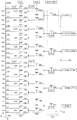
図2に電圧選択回路40、電圧生成回路32の詳細な構成例を示す。なお電圧選択回路40、電圧生成回路32の構成は図2の構成には限定されず、その一部の構成要素を省略したり、他の構成要素を追加するなどの種々の変形実施が可能である。例えば図2では電圧生成回路32が24個の電圧V1〜V24を生成し、これらの電圧V1〜V24が電圧選択回路40に入力される例を示しているが、生成及び入力される複数の電圧の個数はこれに限定されない。また図2では1段目のセレクターブロックBLAを構成するセレクターが、2入力/1出力のセレクターである例を示しているが、例えば4入力/1出力のセレクターなどの他の構成のセレクターであってもよい。2段目、最終段のセレクターブロックBLB、BLFも同様である。また図2ではセレクターブロックの段数が3段である場合を示しているが、セレクターブロックの段数は4段以上であってもよい。また電圧生成回路32は抵抗分割以外の手法により複数の電圧を生成してもよい。
FIG. 2 shows a detailed configuration example of the
図2では電圧生成回路32は、高電位側の電源VDDAのノードと低電位側の電源VSS(GND)のノードとの間に直列に接続された複数の抵抗R1〜R23を有する。電圧生成回路32は、これらの抵抗R1〜R23による電圧分割により、複数の電圧V1〜V24を生成して出力する。
In FIG. 2, the
電圧選択回路40は、セレクターブロックBLA、BLB、BLFを含む。BLA、BLB、BLFは、各々、1段目(初段)、2段目、最終段のセレクターブロックである。
The
1段目のセレクターブロックBLAはセレクターSA1〜SA12を含む。SA1〜SA12の各セレクターは、2入力/1出力のセレクターであり、2つのトランジスターにより構成される。 The first-stage selector block BLA includes selectors SA1 to SA12. Each selector of SA1 to SA12 is a 2-input / 1-output selector and is composed of two transistors.
具体的には、SA1〜SA6の各セレクターは、2つのN型トランジスターにより構成される。例えばセレクターSA1はN型のトランジスターTA1、TA2により構成され、セレクターSA2はN型のトランジスターTA3、TA4により構成される。他のセレクターSA3〜SA6も同様である。一方、SA7〜SA12の各セレクターは、2つのP型のトランジスターにより構成される。例えばセレクターSA7はP型のトランジスターTA13、TA14により構成され、セレクターSA8はP型のトランジスターTA15、TA16により構成される。他のセレクターSA9〜SA12も同様である。 Specifically, each selector of SA1 to SA6 is composed of two N-type transistors. For example, the selector SA1 is composed of N-type transistors TA1 and TA2, and the selector SA2 is composed of N-type transistors TA3 and TA4. The same applies to the other selectors SA3 to SA6. On the other hand, each selector of SA7 to SA12 is composed of two P-type transistors. For example, the selector SA7 is composed of P-type transistors TA13 and TA14, and the selector SA8 is composed of P-type transistors TA15 and TA16. The same applies to the other selectors SA9 to SA12.
そして、この1段目のセレクターブロックBLAには、電圧生成回路32からの複数の電圧V1〜V24が入力される。具体的にはセレクターSA1は、電圧V1、V2が入力され、V1、V2のいずれかを選択して、後段のセレクターブロックBLB(セレクターSB1)に出力する。セレクターSA2は、電圧V3、V4が入力され、V3、V4のいずれかを選択して、後段のセレクターブロックBLB(セレクターSB2)に出力する。他のセレクターSA3〜SA12も同様である。
Then, a plurality of voltages V1 to V24 from the
2段目のセレクターブロックBLBはセレクターSB1〜SB6を含む。SB1〜SB6の各セレクターは、2入力/1出力のセレクターであり、2つのトランジスターにより構成される。具体的には、SB1〜SB3の各セレクターは、2つのN型のトランジスターにより構成される。例えばセレクターSB1はN型のトランジスターTB1、TB2により構成される。他のセレクターSB2、SB3も同様である。一方、SB4〜SB6の各セレクターは、2つのP型のトランジスターにより構成される。例えばセレクターSB4はP型のトランジスターTB7、TB8により構成される。他のセレクターSB5、SB6も同様である。 The second-stage selector block BLB includes selectors SB1 to SB6. Each selector of SB1 to SB6 is a 2-input / 1-output selector, and is composed of two transistors. Specifically, each selector of SB1 to SB3 is composed of two N-type transistors. For example, the selector SB1 is composed of N-type transistors TB1 and TB2. The same applies to the other selectors SB2 and SB3. On the other hand, each selector of SB4 to SB6 is composed of two P-type transistors. For example, the selector SB4 is composed of P-type transistors TB7 and TB8. The same applies to the other selectors SB5 and SB6.
そして、この2段目のセレクターブロックBLBには、1段目(前段)のセレクターブロックBLAにより選択された複数の電圧が入力される。具体的にはセレクターSB1は、前段のセレクターSA1、SA2により選択された2つの電圧が入力され、これらの2つの電圧のいずれかを選択して、後段(最終段)のセレクターブロックBLFのセレクターSFに出力する。セレクターSB2は、前段のセレクターSA3、SA4により選択された2つの電圧が入力され、これらの2つの電圧のいずれかを選択して、後段のセレクターブロックBLFのセレクターSFに出力する。他のセレクターSB3〜SB6も同様である。 Then, a plurality of voltages selected by the selector block BLA of the first stage (previous stage) are input to the selector block BLB of the second stage. Specifically, the selector SB1 is input with two voltages selected by the selectors SA1 and SA2 in the previous stage, and one of these two voltages is selected to select the selector SF of the selector block BLF in the rear stage (final stage). Output to. Two voltages selected by the selectors SA3 and SA4 in the previous stage are input to the selector SB2, one of these two voltages is selected, and the voltage is output to the selector SF of the selector block BLF in the subsequent stage. The same applies to the other selectors SB3 to SB6.
最終段のセレクターブロックBLFは、6入力/1出力のセレクターSFにより構成される。このセレクターSFは、N型のトランジスターTF1〜TF3と、P型のトランジスターTF4〜TF6により構成される。そしてセレクターSFは、前段のセレクターブロックBLBのセレクターSB1〜SB6により選択された6つの電圧が入力され、これらの6つの電圧のいずれかを選択して、D/A変換電圧VDQとして出力する。 The final stage selector block BLF is composed of a 6-input / 1-output selector SF. The selector SF is composed of N-type transistors TF1 to TF3 and P-type transistors TF4 to TF6. Then, the selector SF is input with six voltages selected by the selectors SB1 to SB6 of the selector block BLB in the previous stage, selects one of these six voltages, and outputs the D / A conversion voltage VDQ.
1段目のセレクターブロックBLAを構成するトランジスターTA1〜TA24は、図1のデコーダー30からの1ビットの制御信号SC1(スイッチ制御信号)によりオン、オフ制御される。制御信号SC1は入力データの下位の1ビットに対応する信号である。例えば制御信号SC1がLレベル(論理レベル「0」)である場合には、奇数番目のトランジスターTA1、TA3、TA5・・・TA23がオンになる。一方、制御信号SC1がHレベル(論理レベル「1」)である場合には、偶数番目のトランジスターTA2、TA4、TA6・・・TA24がオンになる。即ち、奇数番目のトランジスターと偶数番目のトランジスターとは、互いに排他的にオン又はオフになる。この排他的なオン、オフは、制御信号SC1とその反転信号を用いることで実現できる。
The transistors TA1 to TA24 constituting the first-stage selector block BLA are controlled on and off by a 1-bit control signal SC1 (switch control signal) from the
2段目のセレクターブロックBLBを構成するトランジスターTB1〜TB12は、デコーダー30からの1ビットの制御信号SC2によりオン、オフ制御される。例えば制御信号SC2がLレベル(「0」)である場合には、奇数番目のトランジスターTB1、TB3・・・TB11がオンになる。一方、制御信号SC2がHレベル(「1」)である場合には、偶数番目のトランジスターTB2、TB4・・・TB12がオンになる。即ち、奇数番目のトランジスターと偶数番目のトランジスターとは、互いに排他的にオン又はオフになる。この排他的なオン、オフは、制御信号SC2とその反転信号を用いることで実現できる。
The transistors TB1 to TB12 constituting the second-stage selector block BLB are controlled on and off by the 1-bit control signal SC2 from the
最終段のセレクターブロックBLFを構成するトランジスターTF1〜TF6は、デコーダー30からの例えば3ビットの制御信号SC3〜SC5によりオン、オフ制御される。例えば制御信号SC3〜SC5により、6つのトランジスターTF1〜TF6のいずれか1つのトランジスターがオンになり、他のトランジスターはオフになる。これにより6入力/1出力のセレクターSFが実現される。
The transistors TF1 to TF6 constituting the selector block BLF in the final stage are controlled on and off by, for example, 3-bit control signals SC3 to SC5 from the
このように本実施形態では、複数段のセレクターブロックBLA、BLB、BLFでは、前段のセレクターブロックが有するセレクターの出力が後段のセレクターブロックが有するセレクターに入力される。1段目(前段)のセレクターブロックBLAが有するセレクターSA1〜SA12の出力が、2段目(後段)のセレクターブロックBLBが有するセレクターSB1〜SB6に入力される。2段目(前段)のセレクターブロックBLBが有するセレクターSB1〜SB6の出力が、最終段(後段)のセレクターブロックBLFが有するセレクターSFに入力される。そして1段目のセレクターブロックBLAには、複数の電圧V1〜V24が入力され、いわゆるトーナメント方式で電圧選択を行うことで、最終段のセレクターブロックBLFから、入力データDIのD/A変換電圧VDQが出力される。 As described above, in the present embodiment, in the plurality of stages of selector blocks BLA, BLB, and BLF, the output of the selector included in the former stage selector block is input to the selector included in the subsequent stage selector block. The outputs of the selectors SA1 to SA12 of the selector block BLA of the first stage (previous stage) are input to the selectors SB1 to SB6 of the selector block BLB of the second stage (second stage). The outputs of the selectors SB1 to SB6 of the selector block BLB of the second stage (previous stage) are input to the selector SF of the selector block BLF of the final stage (second stage). A plurality of voltages V1 to V24 are input to the selector block BLA of the first stage, and by performing voltage selection by a so-called tournament method, the D / A conversion voltage VDQ of the input data DI is transmitted from the selector block BLF of the final stage. Is output.
また複数段のセレクターブロックBLA、BLB、BLFの各々は複数のトランジスターにより構成される。例えばセレクターブロックBLAはトランジスターTA1〜TA24により構成される。セレクターブロックBLBはトランジスターTB1〜TB12により構成される。セレクターブロックBLFはトランジスターTF1〜TF6により構成される。 Further, each of the plurality of stages of selector blocks BLA, BLB, and BLF is composed of a plurality of transistors. For example, the selector block BLA is composed of transistors TA1 to TA24. The selector block BLB is composed of transistors TB1 to TB12. The selector block BLF is composed of transistors TF1 to TF6.
そして、これらの複数のトランジスターにおいて、電源ノード(VDDA、VSS)から遠い側のトランジスターは、電源ノード(VDDA、VSS)から近い側のトランジスターに比べて、低いしきい値電圧に設定されている。 Then, in these a plurality of transistors, the transistor on the side far from the power supply node (VDDA, VSS) is set to a lower threshold voltage than the transistor on the side closer to the power supply node (VDDA, VSS).
例えば最終段のブロックBLFにおいて、P型のトランジスターTF5(第2のトランジスター)は、P型のトランジスターTF6(第1のトランジスター)に比べて、高電位側の電源VDDAのノードから遠い側のトランジスターである。このため、TF5のしきい値電圧VTPMは、TF6のしきい値電圧VTPHよりも低い電圧に設定(VTPM<VTPH)されている。P型のトランジスターTF4(第3のトランジスター)は、P型のトランジスターTF5(第2のトランジスター)に比べて、VDDAのノードから遠い側のトランジスターである。このため、TF4のしきい値電圧VTPLは、TF5のしきい値電圧VTPMよりも低い電圧に設定(VTPL<VTPM)されている。前段のセレクターブロックBLA、BLBのP型のトランジスターTA13〜TA24、TB7〜TB12についても同様である。なおP型のトランジスターのしきい値電圧VTPH、VTPM、VTPLはしきい値電圧の絶対値(|VTPH|、|VTPM|、|VTPL|)を意味する。 For example, in the final stage block BLF, the P-type transistor TF5 (second transistor) is a transistor farther from the node of the power supply VDDA on the high potential side than the P-type transistor TF6 (first transistor). is there. Therefore, the threshold voltage VTPM of TF5 is set to a voltage lower than the threshold voltage VTPH of TF6 (VTPM <VTPH). The P-type transistor TF4 (third transistor) is a transistor farther from the VDDA node than the P-type transistor TF5 (second transistor). Therefore, the threshold voltage VTPL of TF4 is set to a voltage lower than the threshold voltage VTPM of TF5 (VTPL <VTPM). The same applies to the P-type transistors TA13 to TA24 and TB7 to TB12 of the selector blocks BLA and BLB in the previous stage. The threshold voltages VTPH, VTPM, and VTPL of the P-type transistor mean the absolute values of the threshold voltages (| VTPH |, | VTPM |, | VTPL |).
また最終段のブロックBLFにおいて、N型のトランジスターTF2(第2のトランジスター)は、N型のトランジスターTF1(第1のトランジスター)に比べて、低電位側の電源VSSのノードから遠い側のトランジスターである。このため、TF2のしきい値電圧VTNMは、TF1のしきい値電圧VTNHよりも低い電圧に設定(VTNM<VTNH)されている。N型のトランジスターTF3(第3のトランジスター)は、N型のトランジスターTF2(第2のトランジスター)に比べて、VSSのノードから遠い側のトランジスターである。このため、TF3のしきい値電圧VTNLは、TF2のしきい値電圧VTNMよりも低い電圧に設定(VTNL<VTNM)されている。前段のセレクターブロックBLA、BLBのN型のトランジスターTA1〜TA12、TB1〜TB6についても同様である。 Further, in the final stage block BLF, the N-type transistor TF2 (second transistor) is a transistor farther from the node of the power supply VSS on the low potential side than the N-type transistor TF1 (first transistor). is there. Therefore, the threshold voltage VTNM of TF2 is set to a voltage lower than the threshold voltage VTNH of TF1 (VTNM <VTNH). The N-type transistor TF3 (third transistor) is a transistor farther from the VSS node than the N-type transistor TF2 (second transistor). Therefore, the threshold voltage VTNL of TF3 is set to a voltage lower than the threshold voltage VTNM of TF2 (VTNL <VTNM). The same applies to the N-type transistors TA1 to TA12 and TB1 to TB6 of the selector blocks BLA and BLB in the previous stage.
ここで、電源ノード(VDDA、VSS)に近い側の第1のトランジスター(TF1、TF6等)は、しきい値電圧のティピカル値が第1のしきい値電圧(例えば0.6V)である第1の種類(後述するPRH)のトランジスターである。電源ノードから遠い側の第2のトランジスター(TF2、TF5等)は、しきい値電圧のティピカル値が第1のしきい値電圧よりも低い第2のしきい値電圧(例えば0.45V)である第2の種類(後述するPRM)のトランジスターである。電源ノードから更に遠い側の第3のトランジスター(TF3、TF4等)は、しきい値電圧のティピカル値が第2のしきい値電圧よりも低い第3のしきい値電圧(例えば0.25V)である第3の種類(後述するPRL)のトランジスターである。 Here, in the first transistor (TF1, TF6, etc.) on the side close to the power supply node (VDDA, VSS), the typical value of the threshold voltage is the first threshold voltage (for example, 0.6V). It is a transistor of one type (PRH described later). The second transistor (TF2, TF5, etc.) on the side far from the power supply node has a second threshold voltage (for example, 0.45V) in which the typical value of the threshold voltage is lower than the first threshold voltage. A second type of transistor (PRM described later). The third transistor (TF3, TF4, etc.) farther from the power supply node has a third threshold voltage (for example, 0.25V) whose threshold voltage has a typical value lower than that of the second threshold voltage. This is a third type (PRL described later) transistor.
しきい値電圧のティピカル値は、例えば製造プロセス条件がティピカル条件(プロセスばらつきが無い場合の条件)であり、温度が基準温度(例えば25℃)である場合のしきい値電圧である。第1、第2、第3の種類のトランジスターは、例えば製造プロセスが異なるトランジスターである。第1の種類のトランジスター(TF1、TF6等)は、例えば高耐圧用(ハイボルテージ)の製造プロセスにより形成されるトランジスターである。第3の種類のトランジスター(TF3、TF4等)は、例えば低耐圧用(ローボルテージ)の製造プロセスにより形成されるトランジスターである。第2の種類のトランジスター(TF2、TF5等)は、例えば高耐圧用と低耐圧用の間の中耐圧用の製造プロセスにより形成されるトランジスターである。 The typical value of the threshold voltage is, for example, the threshold voltage when the manufacturing process condition is a typical condition (condition when there is no process variation) and the temperature is a reference temperature (for example, 25 ° C.). The first, second, and third types of transistors are, for example, transistors having different manufacturing processes. The first type of transistor (TF1, TF6, etc.) is, for example, a transistor formed by a manufacturing process for high withstand voltage (high voltage). The third type of transistor (TF3, TF4, etc.) is a transistor formed by, for example, a manufacturing process for low withstand voltage (low voltage). The second type of transistor (TF2, TF5, etc.) is a transistor formed by, for example, a manufacturing process for medium withstand voltage between high withstand voltage and low withstand voltage.
例えば第1、第2の種類である第1、第2のトランジスターでは、トランジスターの製造プロセスパラメーターが異なることで、異なるしきい値電圧に設定されている。第3の種類である第3のトランジスターも、トランジスターの製造プロセスパラメーターが異なることで、第1、第2のトランジスターとは異なるしきい値電圧に設定されている。ここで、製造プロセスパラメーターは、トランジスターのチャネル領域等における不純物濃度やゲート酸化膜の厚さなどのパラメータである。例えば不純物濃度を高くしたり、低くすることで、トランジスターのしきい値電圧を設定する。或いは、ゲート酸化膜を薄くしたり、厚くすることで、トランジスターのしきい値電圧を設定する。或いは、製造プロセスパラメーターは、トランジスターの異極ゲートについてのパラメータであってもよい。即ち、トランジスターのゲート(ポリシリコン)について異種のゲート(例えばイオン注入される不純物の濃度や種類が異なるゲート)を用いることで、トランジスターのしきい値電圧を設定する。このようにトランジスターのしきい値電圧を設定する製造プロセスパラメーターとしては種々のパラメータを想定できる。 For example, in the first and second transistors, which are the first and second types, different threshold voltages are set because the manufacturing process parameters of the transistors are different. The third transistor, which is the third type, is also set to a threshold voltage different from that of the first and second transistors because the manufacturing process parameters of the transistors are different. Here, the manufacturing process parameters are parameters such as the impurity concentration in the channel region of the transistor and the thickness of the gate oxide film. For example, the threshold voltage of the transistor is set by increasing or decreasing the impurity concentration. Alternatively, the threshold voltage of the transistor is set by thinning or thickening the gate oxide film. Alternatively, the manufacturing process parameters may be parameters for the different pole gate of the transistor. That is, the threshold voltage of the transistor is set by using different types of gates (for example, gates having different concentrations and types of impurities to be ion-implanted) for the transistor gate (polysilicon). As described above, various parameters can be assumed as the manufacturing process parameters for setting the threshold voltage of the transistor.
また本実施形態では、このようなトランジスターの種類(製造プロセス等)のみならず、トランジスターのゲート長L(チャネル長)の設定により、トランジスターのしきい値電圧を互いに異ならせている。具体的には、後述するようにトランジスターの短チャネル効果や、逆短チャネル効果を有効活用して、トランジスターのしきい値電圧を設定する。 Further, in the present embodiment, the threshold voltage of the transistors is made different from each other by setting not only the type of the transistor (manufacturing process or the like) but also the gate length L (channel length) of the transistor. Specifically, as will be described later, the threshold voltage of the transistor is set by effectively utilizing the short-channel effect and the inverse short-channel effect of the transistor.
例えば図2では、第1のトランジスター(TF1、TF6等)と、第2のトランジスター(TF2、TF5等)とは、ゲート長(チャネル長)が異なっている。また第3のトランジスター(TF3、TF4等)も、他のトランジスターとゲート長を異ならせてもよい。即ち、第1、第2、第3のトランジスターのうちの少なくとも1つのトランジスターは、第1、第2、第3のトランジスターのうちの他のトランジスターとは、ゲート長が異なっている。 For example, in FIG. 2, the gate length (channel length) is different between the first transistor (TF1, TF6, etc.) and the second transistor (TF2, TF5, etc.). Further, the third transistor (TF3, TF4, etc.) may also have a different gate length from other transistors. That is, at least one of the first, second, and third transistors has a different gate length from the other transistors of the first, second, and third transistors.
例えばトランジスターTF1、TF6(第1のトランジスター)のゲート長はL=LTに設定されている。ここで、LTは、第1の種類のトランジスター(PRH)において標準的なゲート長(ティピカルのゲート長)であり、例えばLT=0.4μmである。 For example, the gate lengths of the transistors TF1 and TF6 (first transistor) are set to L = LT. Here, LT is a standard gate length (typical gate length) in the first type transistor (PRH), for example, LT = 0.4 μm.
一方、トランジスターTF2、TF5(第2のトランジスター)のゲート長はL=L1、L4に設定されており、L1、L4は標準的なゲート長LTとは異なっている。例えばL1、L4をLTよりも長くしたり、短くする。なおL1又はL4を、LTと同じ長さに設定してもよい。またL1とL4は、異なる長さでもよいし、同じ長さでもよい。 On the other hand, the gate lengths of the transistors TF2 and TF5 (second transistor) are set to L = L1 and L4, and L1 and L4 are different from the standard gate length LT. For example, L1 and L4 are made longer or shorter than LT. Note that L1 or L4 may be set to the same length as LT. Further, L1 and L4 may have different lengths or may have the same length.
またトランジスターTF3、TF4(第3のトランジスター)のゲート長はL=L2、L3に設定されており、L2、L3は標準的なゲート長LTとは異なっている。例えばL2、L3をLTよりも長くしたり、短くする。なおL2又はL3を、LTと同じ長さに設定してもよい。またL2とL3は、異なる長さでもよいし、同じ長さでもよい。またL2、L3と、前述のL1、L4は、異なる長さでもよいし、同じ長さでもよい。 Further, the gate lengths of the transistors TF3 and TF4 (third transistor) are set to L = L2 and L3, and L2 and L3 are different from the standard gate length LT. For example, L2 and L3 are made longer or shorter than LT. Note that L2 or L3 may be set to the same length as LT. Further, L2 and L3 may have different lengths or may have the same length. Further, L2 and L3 and the above-mentioned L1 and L4 may have different lengths or may have the same length.
また、最終段のセレクターブロックBLFを構成する少なくとも1つのトランジスターのゲート長は、最終段のセレクターブロックBLFを構成する他のトランジスターのゲート長よりも長くなっている。また最終段のセレクターブロックBLFを構成する少なくとも1つのトランジスターのゲート長は、1段目のセレクターブロックBLAを構成するトランジスターのゲート長よりも長くなっている。 Further, the gate length of at least one transistor constituting the final stage selector block BLF is longer than the gate length of the other transistors constituting the final stage selector block BLF. Further, the gate length of at least one transistor constituting the final stage selector block BLF is longer than the gate length of the transistors constituting the first stage selector block BLA.
例えばセレクターブロックBLFを構成するP型のトランジスターTF4又はTF5のゲート長L3、L4は、BLFを構成する他のP型のトランジスターTF6のゲート長LTよりも長くなっている。或いはトランジスターTF4又はTF5のゲート長L3、L4は、1段目のセレクターブロックBLAを構成するP型のトランジスターTA13〜TA24のゲート長LTよりも例えば長くなっている。 For example, the gate lengths L3 and L4 of the P-type transistors TF4 or TF5 constituting the selector block BLF are longer than the gate length LT of the other P-type transistors TF6 constituting the BLF. Alternatively, the gate lengths L3 and L4 of the transistors TF4 or TF5 are, for example, longer than the gate lengths LT of the P-type transistors TA13 to TA24 constituting the first-stage selector block BLA.
またセレクターブロックBLFを構成するN型のトランジスターTF3等のゲート長L2は、BLFを構成する他のN型のトランジスターTF1のゲート長LTよりも長くなっている。或いはトランジスターTF3等のゲート長L2は、1段目のセレクターブロックBLAを構成するN型のトランジスターTA1〜TA12のゲート長LTよりも例えば長くなっている。 Further, the gate length L2 of the N-type transistor TF3 and the like constituting the selector block BLF is longer than the gate length LT of the other N-type transistors TF1 constituting the BLF. Alternatively, the gate length L2 of the transistor TF3 or the like is, for example, longer than the gate length LT of the N-type transistors TA1 to TA12 constituting the first-stage selector block BLA.
このようにトランジスターの種類のみならず、ゲート長も用いて、トランジスターのしきい値電圧を設定すれば、より細かなしきい値電圧の調整が可能になる。これにより、電源電圧が低い場合等においても、例えばトランジスターのオン条件、オフ条件を満たすしきい値電圧の設定が容易になる。またトランジスターのオフリーク電流(オフ時のリーク電流)に起因するD/A変換器の非直線性誤差(DNL等)を抑制するしきい値電圧の設定も可能になる。 In this way, if the threshold voltage of the transistor is set by using not only the type of the transistor but also the gate length, the threshold voltage can be finely adjusted. This makes it easy to set a threshold voltage that satisfies, for example, the on-condition and the off-condition of the transistor even when the power supply voltage is low. It is also possible to set a threshold voltage that suppresses the non-linearity error (DNL, etc.) of the D / A converter due to the off-leakage current (leakage current when off) of the transistor.
なお図2に示すように本実施形態では、最終段のセレクターブロックBLFのセレクターSFは、前段のセレクターブロックBLBから例えば6個(広義にはI個。I≧3)の電圧が入力され、1個のD/A変換電圧VDQを出力するセレクターになっている。即ち最終段のセレクターブロックBLFでは、例えば1つのセレクターSFを用いて、例えば6個の電圧(広義には3個以上の複数の電圧)から、電圧選択を行って、D/A変換電圧VDQを出力する。後述するように最終段のセレクターブロックBLFのトランジスターTF1〜TF6では、その入力電圧が所与の電圧範囲で変化する。このため、トランジスターのオン条件及びオフ条件等を満たすしきい値電圧の設定が難しいという課題がある。この点、図2では、セレクターブロックBLFのセレクターSFは、2入力/1出力のセレクターではなく、6入力/1出力のセレクターになっている。従って、2入力/1出力のセレクターである場合に比べて、セレクターSFを構成するトランジスターTF1〜TF6の入力電圧範囲(電圧変化範囲)を狭くできる。この結果、トランジスターのオン条件、オフ条件等を満たすしきい値電圧の設定を容易化できるという利点がある。 As shown in FIG. 2, in the present embodiment, for example, 6 voltages (I in a broad sense, I ≧ 3) are input from the selector block BLB in the previous stage to the selector SF of the selector block BLF in the final stage, and 1 It is a selector that outputs individual D / A conversion voltage VDQ. That is, in the final stage selector block BLF, for example, one selector SF is used to select a voltage from, for example, six voltages (three or more voltages in a broad sense), and the D / A conversion voltage VDQ is obtained. Output. As will be described later, in the transistors TF1 to TF6 of the selector block BLF in the final stage, the input voltage changes in a given voltage range. Therefore, there is a problem that it is difficult to set a threshold voltage that satisfies the on condition and the off condition of the transistor. In this regard, in FIG. 2, the selector SF of the selector block BLF is not a 2-input / 1-output selector but a 6-input / 1-output selector. Therefore, the input voltage range (voltage change range) of the transistors TF1 to TF6 constituting the selector SF can be narrowed as compared with the case of a 2-input / 1-output selector. As a result, there is an advantage that it is possible to easily set the threshold voltage that satisfies the on condition and the off condition of the transistor.
2.しきい値電圧設定手法
次に本実施形態のしきい値電圧設定手法について詳細に説明する。図3AはP型トランジスターTPのオン条件、オフ条件の説明図である。図3Aに示すようにP型トランジスターTPをオンさせる場合には、そのゲートに例えばVSS=0Vが入力される。P型トランジスターTPがオンするためには、そのゲート・ソース間電圧(絶対値)をしきい値電圧(絶対値)よりも大きくする必要があり、下式(1)に示すオン条件が成立する必要がある。
2. Threshold voltage setting method Next, the threshold voltage setting method of the present embodiment will be described in detail. FIG. 3A is an explanatory diagram of an on condition and an off condition of the P-type transistor TP. When the P-type transistor TP is turned on as shown in FIG. 3A, for example, VSS = 0V is input to the gate. In order for the P-type transistor TP to turn on, the gate-source voltage (absolute value) must be larger than the threshold voltage (absolute value), and the on condition shown in the following equation (1) is satisfied. There is a need.
VIN>VTP+VBS+VPR+VTS (1)
ここでVINは、P型トランジスターTPの入力電圧(ソース・ドレインの入力電圧)である。VTPはP型トランジスターTPの基本的なしきい値電圧であり、VBSは基板バイアス効果によるしきい値電圧の増加分である。即ち、P型トランジスターTPでは、基板電圧が例えばVDDAの電圧となっており、入力電圧VINとは異なっているため、しきい値電圧VTPが基板バイアス効果により電圧VBSだけ増加する。またVPRはプロセスばらつきに起因するしきい値電圧の変動分(プラス方向への変動分)である。VTSは温度変動に起因するしきい値電圧の変動分(プラス方向への変動分)である。即ち、半導体の製造プロセスにはばらつきあるため、このばらつきに起因して、しきい値電圧が高くなる場合がある。また温度変動があった場合にも、しきい値電圧が変動して、高くなる場合がある。従って、P型トランジスターTPがオンするためには、入力電圧VINがVTP+VBS+VPR+VTSよりも高い電圧である必要がある。なおVTPはしきい値電圧の絶対値(|VTP|)を意味する。
VIN> VTP + VBS + VPR + VTS (1)
Here, VIN is the input voltage of the P-type transistor TP (input voltage of the source / drain). VTP is the basic threshold voltage of the P-type transistor TP, and VBS is the increase in the threshold voltage due to the substrate bias effect. That is, in the P-type transistor TP, the substrate voltage is, for example, VDDA, which is different from the input voltage VIN, so that the threshold voltage VTP increases by the voltage VBS due to the substrate bias effect. The VPR is the fluctuation amount of the threshold voltage (the fluctuation amount in the positive direction) due to the process variation. VTS is the fluctuation amount of the threshold voltage (the fluctuation amount in the positive direction) due to the temperature fluctuation. That is, since there are variations in the semiconductor manufacturing process, the threshold voltage may increase due to these variations. Also, when the temperature fluctuates, the threshold voltage may fluctuate and become higher. Therefore, in order for the P-type transistor TP to turn on, the input voltage VIN needs to be higher than VTP + VBS + VPR + VTS. Note that VTP means the absolute value of the threshold voltage (| VTP |).
またP型トランジスターTPが適正にオフするためには、下式(2)に示すオフ条件が成立する必要がある。 Further, in order for the P-type transistor TP to be properly turned off, the off condition shown in the following equation (2) must be satisfied.
VTP−VPR−VTS>0 (2)
ここで、VPRはプロセスばらつきに起因するしきい値電圧の変動分(マイナス方向への変動分)である。VTSは温度変動に起因するしきい値電圧の変動分(マイナス方向への変動分)である。即ち、半導体の製造プロセスにはばらつきあるため、このばらつきに起因して、しきい値電圧が低くなる場合がある。また温度変動があった場合にも、しきい値電圧が変動して、低くなる場合がある。これらのプロセスばらつきや温度変動に起因してしきい値電圧が変動した場合にも、P型トランジスターTPを適正にオフするためには、上式(2)のオフ条件が成立する必要がある。
VTP-VPR-VTS> 0 (2)
Here, VPR is the fluctuation amount of the threshold voltage (variation in the negative direction) due to the process variation. VTS is the fluctuation amount of the threshold voltage due to the temperature fluctuation (the fluctuation amount in the negative direction). That is, since there are variations in the semiconductor manufacturing process, the threshold voltage may be lowered due to the variations. Also, when the temperature fluctuates, the threshold voltage may fluctuate and become lower. Even when the threshold voltage fluctuates due to these process variations and temperature fluctuations, it is necessary to satisfy the off condition of the above equation (2) in order to properly turn off the P-type transistor TP.
図3BはN型トランジスターTNのオン条件、オフ条件の説明図である。図3Bに示すようにN型トランジスターTNをオンさせる場合には、そのゲートに例えばVDDAの電圧(例えば0.9V)が入力される。N型トランジスターTNがオンするためには、そのゲート・ソース間電圧(VDDA−VIN)をしきい値電圧よりも大きくする必要があり、下式(3)に示すオン条件が成立する必要がある。 FIG. 3B is an explanatory diagram of an on condition and an off condition of the N-type transistor TN. When the N-type transistor TN is turned on as shown in FIG. 3B, a voltage of, for example, VDDA (for example, 0.9V) is input to the gate. In order for the N-type transistor TN to turn on, its gate-source voltage (VDDA-VIN) must be larger than the threshold voltage, and the on condition shown in the following equation (3) must be satisfied. ..
VDDA−VIN>VTN+VBS+VPR+VTS (3)
ここで、VTNはN型トランジスターTNの基本的なしきい値電圧であり、VBSは基板バイアス効果によるしきい値電圧の増加分である。VPR、VTSは、上述と同様に、プロセスばらつき、温度変動に起因するしきい値電圧の変動分(プラス方向への変動分)である。
VDDA-VIN> VTN + VBS + VPR + VTS (3)
Here, VTN is the basic threshold voltage of the N-type transistor TN, and VBS is the increase in the threshold voltage due to the substrate bias effect. Similar to the above, VPR and VTS are fluctuations in the threshold voltage (variations in the positive direction) due to process variations and temperature fluctuations.
またN型トランジスターTNが適正にオフするためには、下式(4)に示すオフ条件が成立する必要がある。 Further, in order for the N-type transistor TN to be properly turned off, the off condition shown in the following equation (4) must be satisfied.
VTN−VPR−VTS>0 (4)
VPR、VTSは、上述と同様に、プロセスばらつき、温度変動に起因するしきい値電圧の変動分(マイナス方向への変動分)である。
VTN-VPR-VTS> 0 (4)
VPR and VTS are the fluctuations of the threshold voltage (variations in the negative direction) due to process variations and temperature fluctuations, as described above.
さて、電源VDDAの電圧が、トランジスターのしきい値電圧に対して十分に高い場合には、図1、図2に示すような構成のD/A変換器において、上式(1)〜(4)のようなオン条件、オフ条件を考慮する必要はほとんどない。 When the voltage of the power supply VDDA is sufficiently higher than the threshold voltage of the transistor, the above equations (1) to (4) are used in the D / A converter having the configurations shown in FIGS. 1 and 2. There is almost no need to consider on-conditions and off-conditions such as).
しかしながら、電源VDDAの電圧が低くなり、トランジスターのしきい値電圧に近くなると、上式(1)〜(4)のようなオン条件、オフ条件を考慮しないと、図1、図2のような構成のD/A変換器の適正な動作を実現できないことが判明した。 However, when the voltage of the power supply VDDA becomes low and approaches the threshold voltage of the transistor, the on-conditions and off-conditions as in the above equations (1) to (4) are not taken into consideration, as shown in FIGS. 1 and 2. It was found that the proper operation of the D / A converter with the configuration could not be realized.
例えば本実施形態では、後述するように、トランジスターの仕事関数差を利用した電源回路により、電源VDDAを生成している。このため、VDDAの電圧が例えば0.9Vというように非常に低い電圧になる。そしてVDDA=0.9Vというように低い電圧になると、例えば図2に示すように電源間に多数のトランジスターが配列された電圧選択回路40において、適正な電圧選択を行うことが難しくなる。即ち、電源VDDAの電圧が低くなると、電圧選択回路40を構成するトランジスターのオン条件、オフ条件を満たすことが難しくなり、トーナメント方式による適正な電圧選択を行ってD/A変換電圧VDQを出力することが困難になる。
For example, in the present embodiment, as will be described later, the power supply VDDA is generated by a power supply circuit that utilizes the work function difference of the transistors. Therefore, the voltage of VDDA becomes a very low voltage such as 0.9V. When the voltage becomes as low as VDDA = 0.9V, it becomes difficult to perform appropriate voltage selection in the
例えば図4Aには、図2の最終段のP型のトランジスターTF4〜TF6の入力電圧範囲VR(入力電圧VINの電圧範囲)が示されている。例えばVDDA=0.9Vとした場合に、最終段のP型のトランジスターTF6の入力電圧範囲はVR=0.9〜0.75Vになる。即ち、トランジスターTF6には、電圧生成回路32により生成された電圧V24、V23、V22、V21のいずれかの電圧が、入力電圧VINとして入力される。従って、トランジスターTF6の入力電圧範囲は、電圧V24〜V21に対応するVR=0.9〜0.75Vの範囲になる。
For example, FIG. 4A shows the input voltage range VR (voltage range of the input voltage VIN) of the P-type transistors TF4 to TF6 in the final stage of FIG. For example, when VDDA = 0.9V, the input voltage range of the P-type transistor TF6 in the final stage is VR = 0.9 to 0.75V. That is, any of the voltages V24, V23, V22, and V21 generated by the
また、P型のトランジスターTF5には、電圧生成回路32により生成された電圧V20、V19、V18、V17のいずれかの電圧が、入力電圧VINとして入力される。従って、トランジスターTF6の入力電圧範囲は、電圧V20〜V17に対応するVR=0.75〜0.6Vの範囲になる。同様に、P型のトランジスターTF4の入力電圧範囲はVR=0.6〜0.45Vになる。
Further, any of the voltages V20, V19, V18, and V17 generated by the
図4Bには、図2のN型のトランジスターTF1〜TF3の入力電圧範囲VRが示されている。例えばN型のトランジスターTF3には、電圧V12、V11、V10、V9のいずれかの電圧が、入力電圧VINとして入力される。従って、トランジスターTF3の入力電圧範囲は、電圧V12〜V9に対応するVR=0.45〜0.3Vの範囲になる。同様に、N型のトランジスターTF2、TF1の入力電圧範囲は、各々、VR=0.3〜0.15V、VR=0.15〜0Vになる。 FIG. 4B shows the input voltage range VR of the N-type transistors TF1 to TF3 of FIG. For example, any of the voltages V12, V11, V10, and V9 is input to the N-type transistor TF3 as the input voltage VIN. Therefore, the input voltage range of the transistor TF3 is in the range of VR = 0.45 to 0.3V corresponding to the voltages V12 to V9. Similarly, the input voltage ranges of the N-type transistors TF2 and TF1 are VR = 0.3 to 0.15V and VR = 0.15 to 0V, respectively.
そして図4Aにおいて、P型のトランジスターTF6の入力電圧範囲はVR=0.9〜0.75Vであり、この入力電圧範囲での入力電圧VINの最小電圧VINminは0.75Vである。そして図3Aに示すように、P型のトランジスターTF6のオン条件は、VIN>VTP+VBS+VPR+VTSである。従って、VINmin=0.75Vである場合に、VIN−(VTP+VBS+VPR+VTS)で表されるマージンが最も小さくなり、トランジスターTF6のオン条件が最も厳しくなる。同様に、トランジスターTF5、TF4では、各々、VINmin=0.6V、0.45Vである場合に、オン条件が最も厳しくなる。 In FIG. 4A, the input voltage range of the P-type transistor TF6 is VR = 0.9 to 0.75 V, and the minimum voltage VIN min of the input voltage VIN in this input voltage range is 0.75 V. Then, as shown in FIG. 3A, the ON condition of the P-type transistor TF6 is VIN> VTP + VBS + VPR + VTS. Therefore, when VINmin = 0.75V, the margin represented by VIN− (VTP + VBS + VPR + VTS) becomes the smallest, and the ON condition of the transistor TF6 becomes the strictest. Similarly, in the transistors TF5 and TF4, the on-condition becomes the strictest when VINmin = 0.6V and 0.45V, respectively.
また図4Bにおいて、N型のトランジスターTF3の入力電圧範囲はVR=0.45〜0.3Vであり、この入力電圧範囲でのVDDA−VINの最小電圧(VDDA−VIN)minは0.45Vである。即ち、VDDA=0.9Vであるため、VIN=0.45Vである場合に、VDDA−VINは最小電圧(VDDA−VIN)min=0.9V−0.45V=0.45Vになる。そして図3Bに示すように、N型のトランジスターTF3のオン条件は、VDDA−VIN>VTN+VBS+VPR+VTSである。従って、(VDD−VIN)min=0.45Vである場合に、(VDDA−VIN)−(VTN+VBS+VPR+VTS)で表されるマージンが最も小さくなり、トランジスターTF3のオン条件が最も厳しくなる。同様に、トランジスターTF2、TF1では、各々、(VDD−VIN)min=0.6V、0.75Vである場合に、オン条件が最も厳しくなる。 Further, in FIG. 4B, the input voltage range of the N-type transistor TF3 is VR = 0.45 to 0.3V, and the minimum voltage (VDDA-VIN) min of VDDA-VIN in this input voltage range is 0.45V. is there. That is, since VDDA = 0.9V, when VIN = 0.45V, VDDA-VIN becomes the minimum voltage (VDDA-VIN) min = 0.9V-0.45V = 0.45V. Then, as shown in FIG. 3B, the ON condition of the N-type transistor TF3 is VDDA-VIN> VTN + VBS + VPR + VTS. Therefore, when (VDD-VIN) min = 0.45V, the margin represented by (VDDA-VIN)-(VTN + VBS + VPR + VTS) becomes the smallest, and the ON condition of the transistor TF3 becomes the strictest. Similarly, in the transistors TF2 and TF1, the on-condition becomes the strictest when (VDD-VIN) min = 0.6V and 0.75V, respectively.
このように図4AのP型のトランジスターTF6、TF5、TF4では、オン条件が最も厳しくなるVINmin=0.75V、0.6V、0.45Vの場合に、VIN>VTP+VBS+VPR+VTSのオン条件が満たされるように、しきい値電圧VTPを設定する必要がある。従って、トランジスターTF6、TF5、TF4のしきい値電圧VTPは、各々、少なくとも0.75V、0.6V、0.45Vよりも低い電圧に設定する必要がある。 As described above, in the P-type transistors TF6, TF5, and TF4 of FIG. 4A, the ON condition of VIN> VTP + VBS + VPR + VTS is satisfied when VINmin = 0.75V, 0.6V, 0.45V, which is the strictest ON condition. It is necessary to set the threshold voltage VTP. Therefore, the threshold voltage VTP of the transistors TF6, TF5, and TF4 needs to be set to a voltage lower than at least 0.75V, 0.6V, and 0.45V, respectively.
また図4BのN型のトランジスターTF3、TF2、TF1では、オン条件が最も厳しくなる(VDDA−VIN)min=0.45V、0.6V、0.75Vの場合に、VDDA−VIN>VTN+VBS+VPR+VTSのオン条件が満たされるように、しきい値電圧VTNを設定する必要がある。従って、トランジスターTF3、TF2、TF1のしきい値電圧VTNは、各々、少なくとも0.45V、0.6V、0.75Vよりも低い電圧に設定する必要がある。 Further, in the N-type transistors TF3, TF2, and TF1 of FIG. 4B, when the on condition becomes the strictest (VDDA-VIN) min = 0.45V, 0.6V, 0.75V, VDDA-VIN> VTN + VBS + VPR + VTS is turned on. It is necessary to set the threshold voltage VTN so that the condition is satisfied. Therefore, the threshold voltage VTN of the transistors TF3, TF2, and TF1 needs to be set to a voltage lower than at least 0.45V, 0.6V, and 0.75V, respectively.
そして図4Aに示すように、例えば種類PRH、PRM、PRLのP型のトランジスターでは、しきい値電圧のティピカル値は、各々、0.6V、0.45V、0.25Vになっている。また図4Bに示すように、種類PRL、PRM、PRHのN型のトランジスターでは、しきい値電圧のティピカル値は、各々、0.25V、0.45V、0.6Vになっている。即ち、しきい値電圧(絶対値)は、種類PRHが最も高く、種類PRLが最も低い。 And as shown in FIG. 4A, for example, in the P-type transistors of the types PRH, PRM, and PRL, the typical values of the threshold voltage are 0.6V, 0.45V, and 0.25V, respectively. Further, as shown in FIG. 4B, in the N-type transistors of the types PRL, PRM, and PRH, the typical values of the threshold voltage are 0.25V, 0.45V, and 0.6V, respectively. That is, the threshold voltage (absolute value) has the highest type PRH and the lowest type PRL.
そこで、トランジスターの種類の設定により、しきい値電圧を設定する手法を採用する場合には、例えばTF6については種類PRHのトランジスターを用い、TF5については種類PRMのトランジスターを用い、TF4については種類PRLのトランジスターを用いることが望ましい。また、TF3については種類PRLのトランジスターを用い、TF2については種類PRMのトランジスターを用い、TF1については種類PRHのトランジスターを用いることが望ましい。こうすることで、少なくともトランジスターのオン条件については満たすことが可能になる。 Therefore, when adopting the method of setting the threshold voltage by setting the type of transistor, for example, a transistor of type PRH is used for TF6, a transistor of type PRM is used for TF5, and a type PRL is used for TF4. It is desirable to use the transistor of. Further, it is desirable to use a type PRL transistor for TF3, a type PRM transistor for TF2, and a type PRH transistor for TF1. By doing so, it becomes possible to satisfy at least the on-condition of the transistor.
一方、しきい値電圧VTP、VTNが低くなりすぎると、今度は図3A、図3Bのオフ条件が満たされなくなるという問題が生じる。即ち、しきい値電圧VTP、VTNが低くなりすぎると、VTP−VPR−VTS>0、VTN−VPR−VTS>0のオフ条件が成立しなくなるおそれがある。更に、トランジスターのオフリーク電流に起因するD/A変換器の非直線性誤差(DNL)が許容値を超えてしまうという問題も考慮する必要がある。このため、例えばトランジスターTF6、TF5、TF4のしきい値電圧VTPは、各々、0.75V、0.6V、0.45Vよりも低く、且つ、これらの電圧に近い電圧にすることが望ましい。またトランジスターTF3、TF2、TF1のしきい値電圧VTNは、各々、0.45V、0.6V、0.75Vよりも低く、且つ、これらの電圧に近い電圧にすることが望ましい。 On the other hand, if the threshold voltages VTP and VTN become too low, there arises a problem that the off conditions of FIGS. 3A and 3B cannot be satisfied. That is, if the threshold voltages VTP and VTN become too low, the off conditions of VTP-VPR-VTS> 0 and VTN-VPR-VTS> 0 may not be satisfied. Further, it is necessary to consider the problem that the non-linearity error (DNL) of the D / A converter due to the off-leakage current of the transistor exceeds the permissible value. Therefore, for example, it is desirable that the threshold voltage VTP of the transistors TF6, TF5, and TF4 is lower than 0.75V, 0.6V, and 0.45V, respectively, and close to these voltages. Further, it is desirable that the threshold voltages VTN of the transistors TF3, TF2 and TF1 are lower than 0.45V, 0.6V and 0.75V, respectively, and close to these voltages.
図5は、トランジスターのオフリーク電流に起因する問題について説明する図である。1段目のトランジスターTA13〜TA20は、制御信号SC1により排他的にオン又はオフになる。例えば図5では、奇数番目のトランジスターTA13、TA15・・・TA19がオンになっており、偶数番目のトランジスターTA14、TA16・・・TA20がオフになっている。また2段目のトランジスターTB7〜TB10は、制御信号SC2により排他的にオン又はオフになる。例えば図5では、奇数番目のトランジスターTB7、TB9がオフになっており、偶数番目のトランジスターTB8、TB10がオンになっている。そして最終段のトランジスターTF4、TF5では、TF4がオンになっており、TF5がオフになっている。これにより図5では、電圧V15が選択されて、D/A変換電圧VDQ=V15が出力されている。 FIG. 5 is a diagram illustrating a problem caused by an off-leakage current of a transistor. The first-stage transistors TA13 to TA20 are turned on or off exclusively by the control signal SC1. For example, in FIG. 5, the odd-numbered transistors TA13, TA15 ... TA19 are on, and the even-numbered transistors TA14, TA16 ... TA20 are off. Further, the second-stage transistors TB7 to TB10 are exclusively turned on or off by the control signal SC2. For example, in FIG. 5, the odd-numbered transistors TB7 and TB9 are turned off, and the even-numbered transistors TB8 and TB10 are turned on. Then, in the final stage transistors TF4 and TF5, TF4 is on and TF5 is off. As a result, in FIG. 5, the voltage V15 is selected and the D / A conversion voltage VDQ = V15 is output.
この場合に、例えばオフになっているトランジスターTF5においても、オフリーク電流ILが流れる。このオフリーク電流ILは、電源VDDAから抵抗R23〜R19及びオン状態のトランジスターTA19、TB10を介して、オフ状態のトランジスターTF5を流れ、オン状態のトランジスターTF4に流れ込む。そして、このオフリーク電流ILは、オン状態のトランジスターTB8、TA15を介して、電圧V15のノードに流れ込み、抵抗R14〜R1を介して電源VSS側に流れる。 In this case, for example, the off-leakage current IL also flows in the transistor TF5 that is turned off. This off-leakage current IL flows from the power supply VDDA through the resistors R23 to R19 and the transistors TA19 and TB10 in the on state, through the transistor TF5 in the off state, and into the transistor TF4 in the on state. Then, this off-leakage current IL flows into the node of the voltage V15 via the transistors TB8 and TA15 in the on state, and flows to the power supply VSS side via the resistors R14 to R1.
このようなオフリーク電流ILが流れると、オン状態のトランジスターTF4、TB8、TA15のオン抵抗RONと、オフリーク電流との積に対応する電圧の分だけ、D/A変換電圧VDQが、電圧V15からずれてしまう。また、直列接続された抵抗R1〜R23には、本来は、VDDA−VSSの電圧をR1〜R23の総抵抗値で除算したものに相当する電流Iが流れる前提となっているが、オフリーク電流ILが流れると、この前提が崩れる。即ち電圧生成回路32では、電源VDDAからVSSに電流Iが流れることで、VDDA−VSSの電圧を等分割した電圧V1〜V24が生成される前提となっている。しかしながら、オフリーク電流ILが存在すると、例えば抵抗R23〜R19やR14〜R1に流れる電流がI+ILになってしまうなどの事態が発生し、上記前提が崩れ、D/A変換電圧VDQが電圧V15からずれた電圧になってしまう。そして、D/A変換電圧VDQが本来の電圧からずれた電圧になり、D/A変換器の非直線性誤差(DNL)が許容値(例えば1LSBの電圧)を越えてしまうと、適正なD/A変換を実現できなくなってしまう。
When such an off-leakage current IL flows, the D / A conversion voltage VDQ deviates from the voltage V15 by the voltage corresponding to the product of the on-resistance RON of the on-state transistors TF4, TB8, and TA15 and the off-leakage current. It ends up. Further, it is assumed that a current I corresponding to the voltage of VDDA-VSS divided by the total resistance value of R1 to R23 flows through the resistors R1 to R23 connected in series, but the off-leakage current IL This premise breaks down when That is, in the
トランジスターのオン条件、オフ条件を満たしながら、図5のようなオフリーク電流の問題を回避するためには、図4A、図4Bで説明したトランジスターの種類の設定によるしきい値電圧の設定手法だけでは、不十分な場合がある。 In order to avoid the problem of off-leakage current as shown in FIG. 5 while satisfying the on-condition and the off-condition of the transistor, the threshold voltage setting method by setting the transistor type described with reference to FIGS. 4A and 4B is sufficient. , May be inadequate.
例えば図5において、オフリーク電流ILの電流値を小さくするためには、オフ状態のトランジスターTF5のしきい値電圧を高くする必要がある。トランジスターTF5のしきい値電圧を高くすることで、オフリーク電流ILが減り、オフリーク電流ILに起因する非直線性誤差を低減することが可能になる。 For example, in FIG. 5, in order to reduce the current value of the off-leakage current IL, it is necessary to increase the threshold voltage of the transistor TF5 in the off state. By increasing the threshold voltage of the transistor TF5, the off-leakage current IL can be reduced, and the non-linearity error caused by the off-leakage current IL can be reduced.
しかしながら、例えばオン状態のトランジスターTF4についても、しきい値電圧を高くしてしまうと、今度はオン抵抗RONが増加し、オン抵抗RONに起因する雑音が増加してしまう。このように雑音が増加すると、例えば後述する発振器用の回路装置にD/A変換器を用いた場合に、発振周波数の位相雑音が増加する問題が生じる。 However, for example, even for the transistor TF4 in the on state, if the threshold voltage is increased, the on-resistance RON increases this time, and the noise caused by the on-resistance RON increases. When the noise increases in this way, for example, when a D / A converter is used in the circuit device for the oscillator described later, there arises a problem that the phase noise of the oscillation frequency increases.
このようなトランジスターのオン条件、オフ条件、オフリーク電流に起因する性能低下(非直線性誤差の増加)の回避条件などの種々の条件を満たすためには、しきい値電圧の微調整が必要である。 In order to satisfy various conditions such as transistor on condition, off condition, and avoidance condition of performance deterioration (increase in non-linear error) due to off-leakage current, it is necessary to fine-tune the threshold voltage. is there.
ところが、図4A、図4Bに示すようなトランジスターの種類の設定によるしきい値電圧の設定手法では、しきい値電圧の粗調整は可能であるが、微調整は難しい。例えばトランジスターの種類(製造プロセス)を増やして、しきい値電圧の微調整を実現する手法も考えられるが、この手法では、製造プロセスの種類の増加によるコストの増加や、手間・作業の増加・複雑化などの問題を招く。 However, in the threshold voltage setting method by setting the transistor type as shown in FIGS. 4A and 4B, the threshold voltage can be roughly adjusted, but fine adjustment is difficult. For example, a method of increasing the types of transistors (manufacturing process) to realize fine adjustment of the threshold voltage can be considered, but in this method, the cost increases due to the increase in the types of manufacturing processes, and the labor and work increase. It causes problems such as complication.
そこで本実施形態では、図4A、図4Bに示すようなトランジスターの種類の設定によるしきい値電圧の設定に加えて、トランジスターのゲート長(チャネル長)の調整によるしきい値電圧の設定を行う。例えばトランジスターの種類の設定により、しきい値電圧の粗調整を行い、トランジスターのゲート長の調整により、しきい値電圧の微調整を実現する。こうすることで、トランジスターのオン条件、オフ条件、オフリーク電流に起因する性能低下の回避条件などを満たすことが可能なしきい値電圧の設定手法を実現できる。 Therefore, in the present embodiment, in addition to setting the threshold voltage by setting the transistor type as shown in FIGS. 4A and 4B, the threshold voltage is set by adjusting the gate length (channel length) of the transistor. .. For example, the threshold voltage is roughly adjusted by setting the type of transistor, and the threshold voltage is finely adjusted by adjusting the gate length of the transistor. By doing so, it is possible to realize a threshold voltage setting method that can satisfy the on-condition, the off-condition, the avoidance condition of the performance deterioration due to the off-leakage current, and the like.
例えば図6Aは、種類PRM、PRLのP型、N型トランジスターにおけるゲート長Lとしきい値電圧VTの関係の例を示す図である。例えば種類PRL(低耐圧)のP型トランジスターでは、図6BのF1に示す短チャネル効果により、チャネル値Lが長くなった場合に、しきい値電圧VTが増加する傾向にある。一方、種類PRM(中耐圧)のP型トランジスター、N型トランジスター、及び種類PRL(低耐圧)のN型トランジスターでは、図6BのF2に示す逆短チャネル効果により、ゲート長が長くなった場合に(長チャネル領域において)、しきい値電圧VTが減少する傾向にある。 For example, FIG. 6A is a diagram showing an example of the relationship between the gate length L and the threshold voltage VT in P-type and N-type transistors of types PRM and PRL. For example, in a P-type transistor of type PRL (low withstand voltage), the threshold voltage VT tends to increase when the channel value L becomes long due to the short channel effect shown in F1 of FIG. 6B. On the other hand, in the P-type transistor and N-type transistor of type PRM (medium withstand voltage) and the N-type transistor of type PRL (low withstand voltage), when the gate length becomes long due to the inverse short channel effect shown in F2 of FIG. 6B. The threshold voltage VT tends to decrease (in the long channel region).
例えば図6CのF3、F4は、短チャネル効果の場合の空乏層の様子を模式的に示す図である。F3はゲートによる空乏層であり、F4はソース・ドレイン(N型不純物領域)による空乏層である。短チャネル効果によるしきい値電圧の低下は、F3、F4の空乏層の影響により生じる。即ち空乏層中のアクセプターイオンが表面ポテンシャル(反転層)を低下させることで、しきい値電圧が低下してしまう。例えば図6Cではソース・ドレインによる空乏層がチャネル側に伸びることで、この部分でのアクセプターイオンが表面ポテンシャルを低下させ、しきい値電圧を低下させる。一方、図6DのF5、F6は、逆短チャネル効果の場合の空乏層の様子を模式的に示す図である。F5はゲートによる空乏層であり、F6はソース・ドレインによる空乏層である。図6DのF6では、ソース・ドレインによる空乏層の形状が図6CのF4とは異なっており、例えば空乏層中のアクセプターイオンの影響が少なくなる。 For example, F3 and F4 in FIG. 6C are diagrams schematically showing the state of the depletion layer in the case of the short channel effect. F3 is a depletion layer due to the gate, and F4 is a depletion layer due to the source / drain (N-type impurity region). The decrease in the threshold voltage due to the short channel effect is caused by the influence of the depletion layer of F3 and F4. That is, the acceptor ions in the depletion layer lower the surface potential (inversion layer), so that the threshold voltage is lowered. For example, in FIG. 6C, the depletion layer due to the source and drain extends toward the channel, and the acceptor ions in this portion lower the surface potential and lower the threshold voltage. On the other hand, F5 and F6 in FIG. 6D are diagrams schematically showing the state of the depletion layer in the case of the inverse short channel effect. F5 is a depletion layer due to the gate, and F6 is a depletion layer due to the source and drain. In F6 of FIG. 6D, the shape of the depletion layer due to the source and drain is different from that of F4 of FIG. 6C, and the influence of acceptor ions in the depletion layer is reduced, for example.
本実施形態では、これらの短チャネル効果、逆短チャネル効果を逆手にとって利用し、ゲート長Lによるしきい値電圧の微調整を実現する。例えば種類PRLのP型トランジスターでは、ゲート長Lを長くすることで、短チャネル効果により、しきい値電圧をそのティピカル値から増加させることができる。一方、種類PRMのP型トランジスター、N型トランジスター、及び種類PRLのN型トランジスターでは、ゲート長Lを長くすることで、逆短チャネル効果により、しきい値電圧をそのティピカル値から減少させることができる。これにより、トランジスターのオン条件、オフ条件、オフリーク電流に起因する性能低下の回避条件などを満たすためのしきい値電圧の微調整が可能になる。 In the present embodiment, these short-channel effects and reverse short-channel effects are used in reverse to realize fine adjustment of the threshold voltage by the gate length L. For example, in a P-type transistor of type PRL, the threshold voltage can be increased from its typical value by a short channel effect by increasing the gate length L. On the other hand, in the P-type transistor and N-type transistor of the type PRM, and the N-type transistor of the type PRL, the threshold voltage can be reduced from the typical value by the inverse short channel effect by increasing the gate length L. it can. This makes it possible to fine-tune the threshold voltage to satisfy the on condition, the off condition, the condition for avoiding the performance deterioration due to the off-leakage current, and the like.
なお、本実施形態では基板バイアス効果を利用して、トランジスターのしきい値電圧を設定してもよい。例えば最終段のセレクターブロックBLFを構成する少なくとも1つのトランジスター(TF1〜TF6)を、基板電圧が制御されるトランジスターにすることで、これらのトランジスターのしきい値電圧の微調整を実現する。 In this embodiment, the threshold voltage of the transistor may be set by utilizing the substrate bias effect. For example, by making at least one transistor (TF1 to TF6) constituting the selector block BLF of the final stage a transistor whose substrate voltage is controlled, fine adjustment of the threshold voltage of these transistors is realized.
例えば図7Aでは、基板電圧制御回路42がD/A変換器(回路装置)に設けられ、この基板電圧制御回路42が、P型トランジスターTFPの基板電圧として電圧VBPを供給する。またN型トランジスターTFNの基板電圧として電圧VBNを供給する。P型トランジスターTFPは、図2の最終段のセレクターブロックBLFを構成するP型のトランジスターTF4〜TF6の少なくとも1つである。N型トランジスターTFNは、最終段のセレクターブロックBLFを構成するN型のトランジスターTF1〜TF3の少なくとも1つである。即ち、P型トランジスターTFPの基板電圧としては、通常は高電位側の電源VDDAの電圧(例えば0.9V)が供給されるが、基板電圧制御回路42は、この電圧とは異なる電圧VBPを供給する。またN型トランジスターTFNの基板電圧としては、通常は低電位側の電源VSSの電圧(例えば0V)が供給されるが、基板電圧制御回路42は、この電圧とは異なる電圧VBNを供給する。
For example, in FIG. 7A, a board
例えば図7Bでは、P型トランジスターTFPとしてP型トランジスターTFP1、TFP2が設けられている。これらのP型トランジスターTFP1、TFP2は、互いに電気的に分離されたN型ウェルに形成されている。そして基板電圧制御回路42は、P型トランジスターTFP1のN型ウェルの電位を設定する基板電圧として、電圧VBP1を供給する。またP型トランジスターTFP2のN型ウェルの電位を設定する基板電圧として、電圧VBP2を供給する。こうすることで、P型トランジスターTFP1とTFP2のしきい値電圧を異なる電圧に設定できる。
For example, in FIG. 7B, P-type transistors TFP1 and TFP2 are provided as P-type transistors TFP. These P-type transistors TFP1 and TFP2 are formed in N-type wells that are electrically separated from each other. Then, the substrate
また図7Cでは、N型トランジスターTFNとしてN型トランジスターTFN1、TFN2が設けられている。これらのN型トランジスターTFN1、TFN2は、互いに電気的に分離されたP型ウェルに形成されている。そして基板電圧制御回路42は、N型トランジスターTFN1のP型ウェルの電位を設定する基板電圧として、電圧VBN1を供給する。またN型トランジスターTFN2のP型ウェルの電位を設定する基板電圧として、電圧VBN2を供給する。こうすることで、N型トランジスターTFN1とTFN2のしきい値電圧を異なる電圧に設定できる。
Further, in FIG. 7C, N-type transistors TFN1 and TFN2 are provided as N-type transistors TFN. These N-type transistors TFN1 and TFN2 are formed in P-type wells that are electrically separated from each other. Then, the substrate
以上のように例えば最終段のセクレターを構成するトランジスター(TF1〜TF6)の基板電圧を制御することで、これらのトランジスターのしきい値電圧を設定できる。これにより、トランジスターのオン条件、オフ条件、オフリーク電流に起因する性能低下の回避条件などを満たすためのしきい値電圧の微調整が可能になる。 As described above, for example, the threshold voltage of these transistors can be set by controlling the substrate voltage of the transistors (TF1 to TF6) constituting the final stage section. This makes it possible to fine-tune the threshold voltage to satisfy the on condition, the off condition, the condition for avoiding the performance deterioration due to the off-leakage current, and the like.
但し、基板電圧を制御する手法では、図7B、図7Cに示すように、電気的に分離されたウェル(P型、N型)を形成する必要があるため、回路のレイアウト面積が増加してしまう。これに対してゲート長Lを設定する手法では、例えばゲート長を長くしても、回路のレイアウト面積は殆ど増加しない。従って、この点においてはゲート長Lを設定する手法の方が有利である。 However, in the method of controlling the substrate voltage, as shown in FIGS. 7B and 7C, it is necessary to form electrically separated wells (P type, N type), so that the layout area of the circuit increases. It ends up. On the other hand, in the method of setting the gate length L, for example, even if the gate length is increased, the layout area of the circuit is hardly increased. Therefore, in this respect, the method of setting the gate length L is more advantageous.
3.しきい値電圧の設定の具体例
図8にしきい値電圧の設定の具体例を示す。図8では、P型のトランジスターTA21〜TA24、TB11、TB12、TF6として、種類PRH(高耐圧)のP型のトランジスターを用いている。これらのトランジスターのゲート長はL=0.4μmに設定されている。この種類PRHのP型のトランジスターは、しきい値電圧のティピカル値が0.6Vになっている。例えば図4Aで説明したように最終段のトランジスターTF6の入力電圧範囲は0.9〜0.75Vであり、VINmin=0.75Vである。従って、トランジスターTF6のしきい値電圧VTPHが、種類PRHのしきい値電圧のティピカル値である0.6Vに設定されていても、トランジスターのオン条件、オフ条件等を満たすことができる。
3. 3. Specific example of setting the threshold voltage FIG. 8 shows a specific example of setting the threshold voltage. In FIG. 8, as P-type transistors TA21 to TA24, TB11, TB12, and TF6, P-type transistors of type PRH (high withstand voltage) are used. The gate length of these transistors is set to L = 0.4 μm. The P-type transistor of this type PRH has a typical value of the threshold voltage of 0.6V. For example, as described with reference to FIG. 4A, the input voltage range of the final stage transistor TF6 is 0.9 to 0.75V, and VINmin = 0.75V. Therefore, even if the threshold voltage VTPH of the transistor TF6 is set to 0.6V, which is a typical value of the threshold voltage of the type PRH, the on condition and the off condition of the transistor can be satisfied.
また図8では、P型のトランジスターTA13〜TA20、TB7〜TB10として、種類PRL(低耐圧)のトランジスターを用いている。これらのトランジスターのゲート長はL=0.4μmに設定されている。この種類PRLのトランジスターは、しきい値電圧のティピカル値が0.25Vになっている。 Further, in FIG. 8, as P-type transistors TA13 to TA20 and TB7 to TB10, transistors of type PRL (low withstand voltage) are used. The gate length of these transistors is set to L = 0.4 μm. The transistor of this type PRL has a typical value of the threshold voltage of 0.25V.
このように本実施形態では、電源VDDAのノードから遠い側のトランジスターTA13〜TA20、TB7〜TB10として、しきい値電圧が低い種類PRLのトランジスターを用いている。これにより、これらのトランジスターTA13〜TA20、TB7〜TB10のしきい値電圧を、電源VDDAのノードから近い側のトランジスターTA21〜TA24、TB11、TB12に比べて、低い電圧に設定できるようになる。 As described above, in the present embodiment, the transistors of the type PRL having a low threshold voltage are used as the transistors TA13 to TA20 and TB7 to TB10 on the side far from the node of the power supply VDDA. As a result, the threshold voltages of these transistors TA13 to TA20 and TB7 to TB10 can be set to lower voltages than the transistors TA21 to TA24, TB11, and TB12 on the side closer to the node of the power supply VDDA.
また図8では、N型のトランジスターTA1〜TA4、TB1、TB2、TF1として、種類PRH(高耐圧)のN型のトランジスターを用いている。これらのトランジスターのゲート長はL=0.4μmに設定されている。この種類PRHのN型トランジスターは、しきい値電圧のティピカル値が0.6Vになっている。例えば図4Bで説明したように最終段のトランジスターTF1の入力電圧範囲は0.15〜0Vであり、(VDDA−VIN)min=0.75Vである。従って、トランジスターTF1のしきい値電圧VTNHが、種類PRHのしきい値電圧のティピカル値である0.6Vに設定されていても、トランジスターのオン条件、オフ条件等を満たすことができる。 Further, in FIG. 8, as N-type transistors TA1 to TA4, TB1, TB2, and TF1, N-type transistors of type PRH (high withstand voltage) are used. The gate length of these transistors is set to L = 0.4 μm. The N-type transistor of this type PRH has a typical value of the threshold voltage of 0.6V. For example, as described with reference to FIG. 4B, the input voltage range of the transistor TF1 in the final stage is 0.15 to 0V, and (VDDA-VIN) min = 0.75V. Therefore, even if the threshold voltage VTNH of the transistor TF1 is set to 0.6V, which is a typical value of the threshold voltage of the type PRH, the on condition and the off condition of the transistor can be satisfied.
また図8では、N型のトランジスターTA5〜TA12、TB3〜TB6として、種類PRL(低耐圧)のN型のトランジスターを用いている。これらのトランジスターのゲート長はL=0.4μmに設定されている。この種類PRLのN型のトランジスターは、しきい値電圧のティピカル値が0.25Vになっている。 Further, in FIG. 8, as N-type transistors TA5 to TA12 and TB3 to TB6, N-type transistors of type PRL (low withstand voltage) are used. The gate length of these transistors is set to L = 0.4 μm. The N-type transistor of this type PRL has a typical value of the threshold voltage of 0.25V.
このように本実施形態では、電源VSSのノードから遠い側のトランジスターTA5〜TA12、TB3〜TB6として、しきい値電圧が低い種類PRLのトランジスターを用いている。これにより、これらのトランジスターTA5〜TA12、TB3〜TB6のしきい値電圧を、電源VSSのノードから近い側のトランジスターTA1〜TA4、TB1、TB2に比べて、低い電圧に設定できるようになる。 As described above, in the present embodiment, the transistors TA5 to TA12 and the transistors TB3 to TB6 on the side far from the node of the power supply VSS are the transistors of the type PRL having a low threshold voltage. As a result, the threshold voltage of these transistors TA5 to TA12 and TB3 to TB6 can be set to a lower voltage than the transistors TA1 to TA4, TB1 and TB2 on the side closer to the node of the power supply VSS.
また図8では、最終段のP型のトランジスターTF5として、しきい値電圧のティピカル値が0.45Vである種類PRM(中耐圧)のトランジスターを用いている。そして、このトランジスターTF5のゲート長Lは、標準のゲート長である0.4μmよりも長くなっている。図6Aに示すように、種類PRMのP型トランジスターは、逆短チャネル効果により、ゲート長を長くすることで、しきい値電圧が低くなる。これを利用してトランジスターTF5のしきい値電圧をVTPM<0.45Vに設定する。例えばゲート長Lを2μm以上に設定することで、しきい値電圧VTPMをティピカル値である0.45Vから例えば0.05〜0.1V程度、低い電圧にする。図4Aで説明したようにトランジスターTF5の入力電圧範囲は0.75〜0.6Vであり、VINmin=0.6Vである。従って、トランジスターTF5のしきい値電圧をVTPM<0.45Vに設定することで、トランジスターのオン条件、オフ条件、オフリーク電流に起因する性能低下の回避条件などを満たすことが可能になる。例えば、オン条件であるVINmin=0.6V>VTPM+VBS+VPR+VTSを満たすことができる。またオフ条件であるVTPM−VPR−VTS>0も満たすことができる。またゲート長Lを長くすることよるしきい値電圧の微調整により、オフリーク電流に起因する性能低下の回避条件等も満たすことができる。 Further, in FIG. 8, as the final stage P-type transistor TF5, a transistor of a type PRM (medium withstand voltage) having a typical value of the threshold voltage of 0.45 V is used. The gate length L of the transistor TF5 is longer than the standard gate length of 0.4 μm. As shown in FIG. 6A, the P-type transistor of the type PRM has a lower threshold voltage by increasing the gate length due to the inverse short channel effect. Utilizing this, the threshold voltage of the transistor TF5 is set to VTPM <0.45V. For example, by setting the gate length L to 2 μm or more, the threshold voltage VTPM is lowered from the typical value of 0.45 V to, for example, about 0.05 to 0.1 V. As described with reference to FIG. 4A, the input voltage range of the transistor TF5 is 0.75 to 0.6V, and VINmin = 0.6V. Therefore, by setting the threshold voltage of the transistor TF5 to VTPM <0.45V, it is possible to satisfy the on-condition, the off-condition, the off-leakage current-induced performance deterioration avoidance condition of the transistor, and the like. For example, the on condition VINmin = 0.6V> VTPM + VBS + VPR + VTS can be satisfied. Further, the off condition VTPM-VPR-VTS> 0 can also be satisfied. Further, by finely adjusting the threshold voltage by lengthening the gate length L, it is possible to satisfy the conditions for avoiding performance deterioration due to the off-leakage current.
また図8では、最終段のP型のトランジスターTF4として、しきい値電圧のティピカル値が0.25Vである種類PRL(低耐圧)のトランジスターを用いている。そして、このトランジスターTF4のゲート長Lは、標準のゲート長である0.4μmよりも長くなっている。図6Aに示すように、種類PRLのP型のトランジスターは、短チャネル効果により、ゲート長を長くすることで、しきい値電圧が高くなる。これを利用してトランジスターTF4のしきい値電圧VTPLを、ティピカル値である0.25Vよりも少しだけ高い電圧に設定する。トランジスターTF4の入力電圧範囲は0.6〜0.45Vであり、VINmin=0.45Vである。従って、オン条件であるVINmin=0.45V>VTPL+VBS+VPR+VTSを満たすことができる。またオフ条件であるVTPL−VPR−VTS>0も満たすことができる。またゲート長Lを長くすることによるしきい値電圧の微調整により、オフリーク電流に起因する性能低下の回避条件等も満たすことができる。 Further, in FIG. 8, as the final stage P-type transistor TF4, a type PRL (low withstand voltage) transistor having a threshold voltage typical value of 0.25 V is used. The gate length L of the transistor TF4 is longer than the standard gate length of 0.4 μm. As shown in FIG. 6A, the P-type transistor of the type PRL has a high threshold voltage by increasing the gate length due to the short channel effect. Utilizing this, the threshold voltage VTPL of the transistor TF4 is set to a voltage slightly higher than the typical value of 0.25V. The input voltage range of the transistor TF4 is 0.6 to 0.45V, and VINmin = 0.45V. Therefore, the on condition VINmin = 0.45V> VTPL + VBS + VPR + VTS can be satisfied. Further, the off condition VTPL-VPR-VTS> 0 can also be satisfied. Further, by finely adjusting the threshold voltage by lengthening the gate length L, it is possible to satisfy the conditions for avoiding performance deterioration due to the off-leakage current.
また図8では、最終段のN型のトランジスターTF3として、しきい値電圧のティピカル値が0.45Vである種類PRM(中耐圧)のトランジスターを用いている。そして、このトランジスターTF3のゲート長Lは、標準のゲート長である0.4μmよりも長くなっている。図6Aに示すように、種類PRMのN型のトランジスターは、逆短チャネル効果により、ゲート長を長くすることで、しきい値電圧が低くなる。これを利用してトランジスターTF3のしきい値電圧VTNLを、ティピカル値よりも低い電圧に設定する。例えばゲート長Lを2μm以上に設定することで、しきい値電圧VTNLをティピカル値である0.45Vから例えば0.1〜0.15V程度、低い電圧にする。トランジスターTF3の入力電圧範囲は0.45〜0.3Vであり、(VDDA−VIN)min=0.45Vである。従って、オン条件である(VDDA−VIN)min=0.45V>VTNL+VBS+VPR+VTSを満たすことができる。またオフ条件であるVTNL−VPR−VTS>0も満たすことができる。またゲート長Lを長くすることによるしきい値電圧の微調整により、オフリーク電流に起因する性能低下の回避条件等も満たすことができる。 Further, in FIG. 8, as the final stage N-type transistor TF3, a type PRM (medium withstand voltage) transistor having a threshold voltage typical value of 0.45 V is used. The gate length L of the transistor TF3 is longer than the standard gate length of 0.4 μm. As shown in FIG. 6A, the threshold voltage of the N-type transistor of the type PRM is lowered by increasing the gate length due to the inverse short channel effect. Utilizing this, the threshold voltage VTNL of the transistor TF3 is set to a voltage lower than the typical value. For example, by setting the gate length L to 2 μm or more, the threshold voltage VTNL is lowered from the typical value of 0.45 V to, for example, about 0.1 to 0.15 V. The input voltage range of the transistor TF3 is 0.45 to 0.3V, and (VDDA-VIN) min = 0.45V. Therefore, the on condition (VDDA-VIN) min = 0.45V> VTNL + VBS + VPR + VTS can be satisfied. Further, the off condition VTNL-VPR-VTS> 0 can also be satisfied. Further, by finely adjusting the threshold voltage by lengthening the gate length L, it is possible to satisfy the conditions for avoiding performance deterioration due to the off-leakage current.
また図8では、最終段のN型のトランジスターTF2として、しきい値電圧のティピカル値が0.45Vである種類PRM(中耐圧)のトランジスターを用いている。そして、このトランジスターTF2のゲート長Lは、標準のゲート長である0.4μmよりも少しだけ短くなっている。種類PRMのN型のトランジスターは逆短チャネル効果のトランジスターであるため、ゲート長Lを少しだけ短くすることで、トランジスターTF2のしきい値電圧VTNMを、ティピカル値である0.45Vよりも少しだけ高い電圧に設定できる。トランジスターTF2の入力電圧範囲は0.3〜0.15Vであり、(VDDA−VIN)min=0.6Vである。従って、オン条件である(VDDA−VIN)min=0.6V>VTNM+VBS+VPR+VTSを満たすことができる。またオフ条件であるVTNM−VPR−VTS>0も満たすことができる。またゲート長Lを長くすることによるしきい値電圧の微調整により、オフリーク電流に起因する性能低下の回避条件等も満たすことができる。 Further, in FIG. 8, as the final stage N-type transistor TF2, a type PRM (medium withstand voltage) transistor having a threshold voltage typical value of 0.45 V is used. The gate length L of the transistor TF2 is slightly shorter than the standard gate length of 0.4 μm. Since the N-type transistor of the type PRM is a transistor with an inverse short channel effect, by shortening the gate length L a little, the threshold voltage VTNM of the transistor TF2 is made slightly smaller than the typical value of 0.45V. Can be set to high voltage. The input voltage range of the transistor TF2 is 0.3 to 0.15V, and (VDDA-VIN) min = 0.6V. Therefore, the on condition (VDDA-VIN) min = 0.6V> VTNM + VBS + VPR + VTS can be satisfied. Further, the off condition VTNM-VPR-VTS> 0 can also be satisfied. Further, by finely adjusting the threshold voltage by lengthening the gate length L, it is possible to satisfy the conditions for avoiding performance deterioration due to the off-leakage current.
例えば図8において、オフリーク電流に起因する性能低下の回避条件が厳しくなる場所は、P型トランジスターとN型トランジスターの境界である。即ち、図5のオフリーク電流ILが発生するトランジスターが、P型のトランジスターTF4であり、オン状態となってオフリーク電流ILが流れるトランジスターが、N型のトランジスターTF3である場合である。この場合にも、ゲート長Lによりしきい値電圧を微調整することで、オフリーク電流に起因する非直線性誤差の増加などの性能低下を回避できるようになる。 For example, in FIG. 8, the place where the conditions for avoiding the performance deterioration due to the off-leakage current become strict is the boundary between the P-type transistor and the N-type transistor. That is, the transistor in which the off-leakage current IL is generated in FIG. 5 is the P-type transistor TF4, and the transistor in which the off-leakage current IL flows in the ON state is the N-type transistor TF3. Also in this case, by finely adjusting the threshold voltage with the gate length L, it is possible to avoid performance deterioration such as an increase in non-linearity error due to the off-leakage current.
図9はしきい値電圧の設定の他の具体例である。図9では、1段目のセレクターブロック(BLA)は、128個のトランジスターTA1〜TA128により構成され、2段目のセレクターブロック(BLB)は、32個のトランジスターTB1〜TB32により構成される。即ち、1段目のセレクターブロックは、32個の4入力/1出力のセレクターにより構成され、2段目のセレクターブロックは、16個の2入力/1出力のセレクターにより構成される。また3段目のセレクターブロックは、16個のトランジスターTC1〜TC16により構成され、最終段のセレクターブロックは、8個のトランジスターTF1〜TF8により構成される。即ち、3段目のセレクターブロックは、8個の2入力/1出力のセレクターにより構成され、最終段目のセレクターブロックは、1個の8入力/1出力のセレクターにより構成される。なお、これらのトランジスターに対する種類PRH、PRM、PRLの設定や、ゲート長Lの設定は、図8と同様であるため、詳細な説明は省略する。 FIG. 9 is another specific example of setting the threshold voltage. In FIG. 9, the first-stage selector block (BLA) is composed of 128 transistors TA1 to TA128, and the second-stage selector block (BLB) is composed of 32 transistors TB1 to TB32. That is, the first-stage selector block is composed of 32 4-input / 1-output selectors, and the second-stage selector block is composed of 16 2-input / 1-output selectors. The third-stage selector block is composed of 16 transistors TC1 to TC16, and the final-stage selector block is composed of eight transistors TF1 to TF8. That is, the third-stage selector block is composed of eight 2-input / 1-output selectors, and the final-stage selector block is composed of one 8-input / 1-output selector. Since the settings of the types PRH, PRM, and PRL and the setting of the gate length L for these transistors are the same as those in FIG. 8, detailed description thereof will be omitted.
4.電源回路
図10Aに本実施形態の回路装置500と、回路装置500を含む電子機器の構成例を示す。なお電子機器や回路装置500は他の構成要素を含むことができるが、ここでは図示を省略している。
4. Power supply circuit FIG. 10A shows a configuration example of the
回路装置500は、図1〜図9で説明した本実施形態のD/A変換器100と、D/A変換器100に電源電圧(VDDA)を供給する電源回路44を含む。そして電源回路44は、トランジスターの仕事関数差に基づき生成された基準電圧を生成する基準電圧生成回路45を有し、基準電圧生成回路45により生成された基準電圧を電源電圧(VDDA)として、D/A変換器100に供給する。
The
図10Aの電子機器は、スイッチングレギュレーター560(広義には外部電源回路)と、回路装置500を含む。回路装置500の電源回路44には、スイッチングレギュレーター560から外部電源(VDD)が供給される。
The electronic device of FIG. 10A includes a switching regulator 560 (in a broad sense, an external power supply circuit) and a
スイッチングレギュレーター560は、例えばトランジスター等のスイッチ素子とインダクター、キャパシター、ダイオード等で構成される。そして、スイッチ素子がオンになるオン期間では、電源(VDDE)とインダクターの一端がスイッチ素子を介して接続されてインダクターが駆動されると共にキャパシターに電荷が供給される。スイッチ素子がオフになるオフ期間では、電源とインダクターの一端が遮断され、インダクターに蓄えられたエネルギーが放電されてダイオードを介したキャパシターに電荷が供給される。スイッチングレギュレーター560の出力電圧をフィードバックすることにより、オン期間とオフ期間のデューティーが制御され、出力電圧が一定に保たれる。
The
なお、スイッチングレギュレーター560の構成はこれに限定されず、スイッチ素子のオンオフにより断続的に電源を接続及び遮断するDC−DCコンバーターであればよい。
The configuration of the
このようなスイッチングレギュレーター560は、リニアレギュレーターのような抵抗による電力ロスがほとんどないため、リニアレギュレーターに比べて低消費電力である。一方、スイッチ素子によりチョッピングを行うため、リニアレギュレーターに比べて、生成される電源電圧(VDD)のノイズが大きい。この点、図10Aの構成では、仕事関数差に基づき電源電圧(VDDA)を生成することで、電源回路44の消費電力を抑えつつ、高いPSRR(Power Supply Rejection Ratio)を実現することが可能であり、スイッチングレギュレーター560と電源回路44を含めた電源システム全体としての低消費電力化や低ノイズ化が可能になる。例えばPSRRが高ければ、スイッチングレギュレーター560が生成する電源電圧(VDD)のノイズを十分に低減できる。
Such a
図10Bに、基準電圧生成回路45の第1の構成例を示す。図10Bの基準電圧生成回路45は、トランジスターTAa、TAb、TAc、TAd、TAe、抵抗RNA、RPA、RGA、キャパシターCA、電流源IGAを含む。
FIG. 10B shows a first configuration example of the reference
トランジスターTAaとトランジスターTAbは、カレントミラー回路を構成し、トランジスターTAcとトランジスターTAdに電流を供給する。トランジスターTAcとトランジスターTAdは差動対を構成する。電流源IGAは、差動対にバイアス電流を供給する。トランジスターTAa、TAbは例えばP型トランジスター(広義には第1導電型のトランジスター)であり、トランジスターTAc、TAdはN型トランジスター(広義には第2導電型のトランジスター)である。またトランジスターTAa、TAb、TAdはエンハンスメント型のトランジスターであり、トランジスターTAcはデプレッション型のトランジスターである。 The transistor TAa and the transistor TAb form a current mirror circuit, and supply a current to the transistor TAc and the transistor TAd. The transistor TAc and the transistor TAd form a differential pair. The current source IGA supplies a bias current to the differential pair. Transistors TAa and TAb are, for example, P-type transistors (in a broad sense, first conductive type transistors), and transistors TAc and TAd are N-type transistors (in a broad sense, second conductive type transistors). Further, the transistors TAa, TAb and TAd are enhancement type transistors, and the transistor TAc is a depletion type transistor.
トランジスターTAa、TAbのソースにはVDDの電源電圧が供給され、トランジスターTAa、TAbのゲート電極はトランジスターTAcのドレインのノードNAaに接続される。 The power supply voltage of VDD is supplied to the source of the transistors TAa and TAb, and the gate electrodes of the transistors TAa and TAb are connected to the node NAa of the drain of the transistor TAc.
トランジスターTAc、TAdは、ノードNAa、NAbとノードNAf、NAcとの間に設けられる。またノードNAfとノードNAcとの間には抵抗RNAが設けられる。トランジスターTAcのゲート電極には、VSSの電源電圧が入力される。トランジスターTAdのゲート電極は、ノードNAdに接続される。電流源IGAは、ノードNAcとVSSの電源ノードとの間に設けられる。 Transistors TAc and TAd are provided between the nodes NAa and NAb and the nodes NAf and NAc. Further, a resistance RNA is provided between the node NAf and the node NAc. The power supply voltage of VSS is input to the gate electrode of the transistor TAC. The gate electrode of the transistor TAd is connected to the node NAd. The current source IGA is provided between the node NAc and the power node of VSS.
トランジスターTAeはデプレッション型のN型トランジスターである。トランジスターTAeは、VDDの電源ノードNDGと出力ノードNAe(抵抗RPAの一端)との間に設けられ、そのゲート電極に差動対の出力ノードNAbが接続される。即ち、トランジスターTAeは、トランジスターTAdのドレイン電圧に基づきゲート電圧が制御される。キャパシターCAは、ノードNAbとVSSのノードとの間に設けられる。抵抗RPAは、出力ノードNAeとノードNAdの間に設けられ、一端(ノードNAe)の電圧を、基準電圧である電源電圧VDDAとして出力する。抵抗RGAは、ノードNAdとVSSのノードとの間に設けられる。 The transistor TAe is a depletion type N-type transistor. The transistor TAe is provided between the power supply node NDG of VDD and the output node NAe (one end of the resistor RPA), and the output node NAb of the differential pair is connected to the gate electrode. That is, the gate voltage of the transistor TAe is controlled based on the drain voltage of the transistor TAd. The capacitor CA is provided between the node NAb and the VSS node. The resistor RPA is provided between the output node NAe and the node NAd, and outputs the voltage at one end (node NAe) as the power supply voltage VDDA which is the reference voltage. The resistor RGA is provided between the node NAd and the node of VSS.
トランジスターTAdは、トランジスターTAcとはゲート電極の導電性が異なるトランジスターになっている。例えばトランジスターTAcのゲート電極はN型であり、トランジスターTAdのゲート電極はP型となっている。例えばトランジスターTAcとTAdは、基板の不純物濃度やチャネルの不純物濃度は同じであるが、ゲート電極の導電性が異なっており、ゲート電極の不純物濃度が異なっている。 The transistor TAd is a transistor whose gate electrode has a different conductivity from that of the transistor TAC. For example, the gate electrode of the transistor TAC is N-type, and the gate electrode of the transistor TAC is P-type. For example, the transistors TAc and TAd have the same impurity concentration on the substrate and the same channel impurity concentration, but differ in the conductivity of the gate electrode and differ in the impurity concentration of the gate electrode.
例えば、MOSトランジスターのしきい値電圧は、Vth=φMS−QSS/COX+2φF+QD/COXと表すことができる。ここでφMSは、ゲート電極と基板の仕事関数差であり、QSSは酸化膜内の固定電荷であり、COXはゲート酸化膜の単位面積当たりの容量であり、φFはフェルミ準位であり、QDは空乏層内の電荷である。トランジスターTAcのN型ゲート電極の不純物濃度と、トランジスターTAdのP型ゲート電極の不純物濃度の設定により、デプレッション型のトランジスターTAcのしきい値電圧VT1は例えば−0.52Vに設定されており、エンハンスメント型のトランジスターTAdのしきい値電圧VT2は例えば0.45Vに設定されている。従って、基準電圧生成回路45の出力ノードNAeには、VT2−VT1=0.97Vの基準電圧が、電源電圧VDDAとして出力されるようになる。即ち、スイッチングレギュレーター560からの電源VDDが変動した場合にも、一定電圧の電源電圧VDDAを供給することが可能になる。
For example, the threshold voltage of the MOS transistor can be expressed as Vth = φ MS −Q SS / C OX + 2φ F + Q D / C OX . Here, φ MS is the work function difference between the gate electrode and the substrate, Q SS is the fixed charge in the oxide film, COX is the capacitance per unit area of the gate oxide film, and φ F is the Fermi level. in and, Q D is the charge in the depletion layer. The threshold voltage VT1 of the depletion type transistor TAc is set to, for example, -0.52V by setting the impurity concentration of the N-type gate electrode of the transistor TAc and the impurity concentration of the P-type gate electrode of the transistor TAd, which is an enhancement. The threshold voltage VT2 of the type transistor TAd is set to, for example, 0.45V. Therefore, the reference voltage of VT2-VT1 = 0.97V is output to the output node NAe of the reference
図11に、基準電圧生成回路45の第2の構成例を示す。図11の基準電圧生成回路45は、第1の仕事関数差アンプREG1、第2の仕事関数差アンプREG2を含む。第1の仕事関数差アンプREG1は、トランジスターTBa、TBb、TBc、TBd、TBe、抵抗RNB、RPB、RGB、キャパシターCB、電流源IGBを含む。第2の仕事関数差アンプREG2は、トランジスターTAa、TAb、TAc、TAd、TAe、抵抗RNA、RPA、RGA、キャパシターCA、電流源IGAを含む。
FIG. 11 shows a second configuration example of the reference
第1、第2の仕事関数差アンプREG1、REG2の構成は、図10Bの回路の構成と同様である。即ち、図11では、図10Bの構成の回路が直列に接続された構成となっている。具体的には、第1の仕事関数差アンプREG1が、基準電圧である出力電圧Vregを生成し、この出力電圧Vregが、第2の仕事関数差アンプREG2の電源ノードNDGに対して供給される。即ち、同じ回路構成の仕事関数差アンプが2段積みとなる構成となっている。そして第2の仕事関数差アンプREG2により生成された基準電圧が、電源電圧VDDAとして出力される。具体的には、第1の仕事関数差アンプREG1が電圧Vreg=0.97Vを出力し、第2の仕事関数差アンプREG2が電圧Vreg=0.97Vを電源として電源電圧VDDA=0.9Vを出力する。 The configurations of the first and second work function difference amplifiers REG1 and REG2 are the same as those of the circuit of FIG. 10B. That is, in FIG. 11, the circuits having the configuration of FIG. 10B are connected in series. Specifically, the first work function difference amplifier REG1 generates an output voltage Vreg which is a reference voltage, and this output voltage Vreg is supplied to the power supply node NDG of the second work function difference amplifier REG2. .. That is, the work function difference amplifiers having the same circuit configuration are stacked in two stages. Then, the reference voltage generated by the second work function difference amplifier REG2 is output as the power supply voltage VDDA. Specifically, the first work function difference amplifier REG1 outputs a voltage Vreg = 0.97V, and the second work function difference amplifier REG2 uses a voltage Vreg = 0.97V as a power source and a power supply voltage VDDA = 0.9V. Output.
このように、第1の仕事関数差アンプREG1と第2の仕事関数差アンプREG2を直列に接続することによって、図10Bのような1段の仕事関数差アンプよりも、更にPSRRを向上できる。 In this way, by connecting the first work function difference amplifier REG1 and the second work function difference amplifier REG2 in series, the PSRR can be further improved as compared with the one-stage work function difference amplifier as shown in FIG. 10B.
以上に説明した図10A〜図11の構成によれば、トランジスターの仕事関数差に基づいて基準電圧が生成され、その基準電圧が電源電圧VDDAとして、D/A変換器100等の回路装置500の各回路に供給される。これにより、D/A変換器100や回路装置500の低消費電力化を実現できる。
According to the configurations of FIGS. 10A to 11 described above, a reference voltage is generated based on the work function difference of the transistors, and the reference voltage is set as the power supply voltage VDDA of the
例えば本実施形態の比較例として、基準電圧生成回路45としてバンドギャップリファレンス回路を用いる手法が考えられる。しかしながら、バンドギャップリファレンス回路は、バンドギャップ電圧の温度依存性をキャンセルするために複数のバイポーラートランジスターを用いており、それらに流すバイアス電流等によって、消費電流が大きい回路となってしまう。そのため、高いPSRRを維持しつつ、消費電流を絞ることが難しいという課題がある。電源のノイズ特性は、例えば回路装置500を発振器に適用した場合には、発振器の発振信号の精度(例えば位相ノイズ特性)に影響する。このため、高いPSRRが必要であり、この点からバンドギャップリファレンス回路を用いた電源回路では低消費電力化に限界がある。
For example, as a comparative example of the present embodiment, a method using a bandgap reference circuit as the reference
この点、本実施形態の電源回路44ではトランジスターの仕事関数差に基づいて電源電圧VDDAを生成することで、バンドギャップリファレンス回路を用いる場合に比べて消費電流を低下させつつ、高いPSRRを維持できる。例えば、ゲート電極と基板の間の仕事関数が異なるトランジスターTAcとトランジスターTAdで差動対を構成し、その差動対の出力をトランジスターTAeにより差動対にフィードバックすることで、電源電圧VDDA(基準電圧)を生成できる。このように、仕事関数差を用いた場合には簡素な構成で電源回路44を構成できるので、バイアス電流を小さくすることが容易である。
In this respect, in the
また本実施形態の電源回路44によれば、高いPSRRが得られることから、より上流側の外部電源として、図10Aに示すようにスイッチングレギュレーター560を用いることが可能となる。即ち、スイッチングレギュレーター560により発生するノイズを、高いPSSRの電源回路44により除去できる。
Further, according to the
また図10B、図11に示す基準電圧生成回路45は、バンドギャップリファレンス回路に比べて、回路規模が小さいという利点がある。このため、例えば回路装置の各回路ブロック毎に基準電圧生成回路45を設けるというような、電源回路44の構成が可能になる。例えばD/A変換器100を含むD/A変換部には、第1の基準電圧生成回路が電源電圧を供給し、後述するA/D変換部、処理部には、各々、第2、第3の基準電圧生成回路が電源電圧を供給するというような構成が可能になる。これにより基準電圧生成回路を用いた電源分離が可能になる。
Further, the reference
そして図10A〜図11で説明したような電源回路44を用いた場合には、VDDAの電圧がトランジスターの仕事関数差を用いて生成されるため、VDDAが例えば0.9Vというように非常に低い電圧になる。従って、VDDAが供給されるD/A変換器100の適正なD/A変換(電圧選択)を実現できなくなるおそれがある。
When the
この点、図1〜図9で説明した本実施形態のD/A変換器100では、前述したように、電源ノードから遠い側のトランジスターのしきい値電圧を、近い側のトランジスターに比べて低い電圧に設定する手法を採用している。また、しきい値電圧の設定を、トランジスターの種類による粗調整やゲート長による微調整により実現している。従って、VDDAの電圧が例えば0.9Vというように非常に低い電圧である場合にも、D/A変換器100の適正なD/A変換を実現することが可能になる。
In this regard, in the D /
5.回路装置
次に本実施形態のD/A変換器100を有する回路装置の構成の一例について説明する。例えば図12の回路装置は、DTCXOやOCXO等のデジタル方式の発振器を実現する回路装置(半導体チップ)である。この回路装置と振動子XTALをパッケージに収納することで、デジタル方式の発振器が実現される。
5. Circuit device Next, an example of the configuration of the circuit device having the D /
図12の回路装置は、A/D変換部20、処理部50、発振信号生成回路140を含む。また回路装置は温度センサー部10、バッファー回路160を含むことができる。なお回路装置の構成は図12の構成には限定されず、その一部の構成要素(例えば温度センサー部、バッファー回路、A/D変換部等)を省略したり、他の構成要素を追加するなどの種々の変形実施が可能である。
The circuit device of FIG. 12 includes an A /
振動子XTALは、例えば水晶振動子等の圧電振動子である。振動子XTALは恒温槽内に設けられるオーブン型振動子(OCXO)であってもよい。振動子XTALは共振器(電気機械的な共振子又は電気的な共振回路)であってもよい。振動子XTALとしては、圧電振動子、SAW(Surface Acoustic Wave)共振子、MEMS(Micro Electro Mechanical Systems)振動子等を採用できる。振動子XTALの基板材料としては、水晶、タンタル酸リチウム、ニオブ酸リチウム等の圧電単結晶や、ジルコン酸チタン酸鉛等の圧電セラミックス等の圧電材料、又はシリコン半導体材料等を用いることができる。振動子XTALの励振手段としては、圧電効果によるものを用いてもよいし、クーロン力による静電駆動を用いてもよい。 The oscillator XTAL is a piezoelectric oscillator such as a crystal oscillator. The oscillator XTAL may be an oven-type oscillator (OCXO) provided in a constant temperature bath. The oscillator XTAL may be a resonator (electromechanical resonator or electrical resonance circuit). As the oscillator XTAL, a piezoelectric oscillator, a SAW (Surface Acoustic Wave) resonator, a MEMS (Micro Electro Mechanical Systems) oscillator, or the like can be adopted. As the substrate material of the oscillator XTAL, a piezoelectric single crystal such as crystal, lithium tantalate, lithium niobate or the like, a piezoelectric material such as piezoelectric ceramics such as lead zirconate titanate, or a silicon semiconductor material can be used. As the exciting means of the oscillator XTAL, one by a piezoelectric effect may be used, or electrostatic drive by a Coulomb force may be used.
温度センサー部10は、温度検出電圧VTDを出力する。具体的には、環境(回路装置)の温度に応じて変化する温度依存電圧を、温度検出電圧VTDとして出力する。
The
A/D変換部20は、温度センサー部10からの温度検出電圧VTDのA/D変換を行って、温度検出データDTDを出力する。例えば温度検出電圧VTDのA/D変換結果に対応するデジタルの温度検出データDTD(A/D結果データ)を出力する。A/D変換部20のA/D変換方式としては、例えば逐次比較方式や逐次比較方式に類似する方式などを採用できる。なおA/D変換方式はこのような方式には限定されず、種々の方式(計数型、並列比較型又は直並列型等)を採用できる。このA/D変換部20にも図1、図2等の本実施形態のD/A変換器を用いることができる。
The A /
処理部50(DSP部:デジタル信号処理部)は種々の信号処理を行う。例えば処理部50(温度補償部)は、温度検出データDTDに基づいて発振周波数(発振信号の周波数)の温度補償処理を行う。そして発振周波数の周波数制御データDDSを出力する。具体的には処理部50は、温度に応じて変化する温度検出データDTD(温度依存データ)と、温度補償処理用の係数データ(近似関数の係数のデータ)などに基づいて、温度変化があった場合にも発振周波数を一定にするための温度補償処理を行う。この処理部50は、ゲートアレイ等のASIC回路により実現してもよいし、プロセッサーとプロセッサー上で動作するプログラムにより実現してもよい。
The processing unit 50 (DSP unit: digital signal processing unit) performs various signal processing. For example, the processing unit 50 (temperature compensation unit) performs temperature compensation processing for the oscillation frequency (frequency of the oscillation signal) based on the temperature detection data DTD. Then, the frequency control data DDS of the oscillation frequency is output. Specifically, the
発振信号生成回路140は発振信号SSCを生成する。例えば発振信号生成回路140は、処理部50からの周波数制御データDDSと振動子XTALを用いて、周波数制御データDDSにより設定される発振周波数の発振信号SSCを生成する。一例としては、発振信号生成回路140は、周波数制御データDDSにより設定される発振周波数で振動子XTALを発振させて、発振信号SSCを生成する。
The oscillation
なお発振信号生成回路140は、ダイレクト・デジタル・シンセサイザー方式で発振信号SSCを生成する回路であってもよい。例えば振動子XTAL(固定発振周波数の発振源)の発振信号をリファレンス信号として、周波数制御データDDSで設定される発振周波数の発振信号SSCをデジタル的に生成してもよい。
The oscillation
発振信号生成回路140は、D/A変換部80と発振回路150を含むことができる。但し発振信号生成回路140は、このような構成には限定されず、その一部の構成要素を省略したり、他の構成要素を追加するなどの種々の変形実施が可能である。
The oscillation
D/A変換部80は、処理部50からの周波数制御データDDS(処理部の出力データ)のD/A変換を行う。D/A変換部80に入力される周波数制御データDDSは、処理部50による温度補償処理後の周波数制御データ(周波数制御コード)である。
The D /
発振回路150は、D/A変換部80の出力電圧VQと振動子XTALを用いて、発振信号SSCを生成する。発振回路150は、第1、第2の振動子用端子(振動子用パッド)を介して振動子XTALに接続される。例えば発振回路150は、振動子XTAL(圧電振動子、共振子等)を発振させることで、発振信号SSCを生成する。具体的には発振回路150は、D/A変換部80の出力電圧VQを周波数制御電圧(発振制御電圧)とした発振周波数で、振動子XTALを発振させる。例えば発振回路150が、電圧制御により振動子XTALの発振を制御する回路(VCO)である場合には、発振回路150は、周波数制御電圧に応じて容量値が変化する可変容量キャパシター(バリキャップ等)を含むことできる。
The
なお、前述のように発振回路150はダイレクト・デジタル・シンセサイザー方式により実現してもよく、この場合には振動子XTALの発振周波数はリファレンス周波数となり、発振信号SSCの発振周波数とは異なる周波数になる。
As described above, the
バッファー回路160は、発振信号生成回路140(発振回路150)で生成された発振信号SSCのバッファリングを行って、バッファリング後の信号SQを出力する。即ち、外部の負荷を十分に駆動できるようにするためのバッファリングを行う。信号SQは例えばクリップドサイン波信号である。但し信号SQは矩形波信号であってもよい。或いはバッファー回路160は、信号SQとしてクリップドサイン波信号と矩形波信号の両方の出力が可能な回路であってもよい。
The
図13に本実施形態の回路装置の詳細な構成例を示す。図13ではD/A変換部80が、変調回路90とD/A変換器100とフィルター回路120を含む。
FIG. 13 shows a detailed configuration example of the circuit device of the present embodiment. In FIG. 13, the D /
D/A変換部80の変調回路90は、処理部50からi=(n+m)ビットの周波数制御データDDSを受ける(i、n、mは1以上の整数)。一例としてはi=20、n=16、m=4である。そして変調回路90は、周波数制御データDDSのmビット(例えば4ビット)のデータに基づいて、周波数制御データDDSのnビット(例えば16ビット)のデータを変調する。具体的には変調回路90は、周波数制御データDDSのPWM変調を行う。なお変調回路90の変調方式はPWM変調(パルス幅変調)には限定されず、例えばPDM変調(パルス密度変調)等のパルス変調であってもよく、パルス変調以外の変調方式であってもよい。例えば周波数制御データDDSのnビットのデータに対して、mビットのディザー処理(ディザリング処理)を行うことでビット拡張(nビットからiビットへのビット拡張)を実現してもよい。
The
D/A変換器100は、変調回路90により変調されたnビットのデータのD/A変換を行う。例えばn=16ビットのデータのD/A変換を行う。
The D /
フィルター回路120は、D/A変換器100の出力電圧VDAを平滑化する。例えばローパスフィルター処理を行って出力電圧VDAを平滑化する。このようなフィルター回路120を設けることで、例えばPWM変調された信号のPWM復調が可能になる。このフィルター回路120のカットオフ周波数は、変調回路90のPWM変調の周波数に応じて設定できる。即ちD/A変換器100からの出力電圧VDAの信号は、PWM変調の基本周波数及び高調波成分のリプルを含むため、フィルター回路120により、このリップルを減衰させる。なおフィルター回路120としては、例えば抵抗又はキャパシター等の受動素子を用いたパッシブフィルターを採用できる。但しフィルター回路120としてSCFなどのアクティブフィルターを用いることも可能である。
The
例えば温度補償型発振器であるTCXOでは、周波数精度の向上と低消費電力化への要求がある。例えばGPS内蔵の時計や脈波等の生体情報の測定機器などのウェアラブル機器では、バッテリーによる動作継続時間を長くする必要がある。このため、基準信号源となるTCXOに対しては、周波数精度を確保しながら、より低消費電力であることが要求される。 For example, in TCXO, which is a temperature-compensated oscillator, there is a demand for improvement in frequency accuracy and reduction in power consumption. For example, in a wearable device such as a clock with a built-in GPS or a device for measuring biological information such as a pulse wave, it is necessary to lengthen the operation duration by the battery. Therefore, the TCXO, which is the reference signal source, is required to have lower power consumption while ensuring frequency accuracy.
また通信端末と基地局との通信方式としては種々の方式が提案されている。例えばTDD(Time Division Duplex)方式では、各機器は割り当てられたタイムスロットにおいてデータを送信する。そしてタイムスロット(上がり回線スロット、下り回線スロット)の間にガードタイムが設定されることで、タイムスロットが重なるのが防止される。次世代の通信システムでは、例えば1つの周波数帯域(例えば50GHz)を用いて、TDD方式でデータ通信することが提案されている。 Further, various methods have been proposed as communication methods between the communication terminal and the base station. For example, in the TDD (Time Division Duplex) system, each device transmits data in an assigned time slot. Then, by setting a guard time between the time slots (up line slot, down line slot), it is possible to prevent the time slots from overlapping. In next-generation communication systems, it has been proposed to carry out data communication in a TDD manner, for example, using one frequency band (for example, 50 GHz).
しかしながら、このようなTDD方式を採用した場合には、各機器において時刻同期を行う必要があり、正確な絶対時刻の計時が要求される。このような要求を実現するために、例えば各機器に、基準信号源として原子時計(原子発振器)を設ける手法も考えられるが、機器の高コスト化を招いたり、機器が大型化するなどの問題が生じる。 However, when such a TDD method is adopted, it is necessary to synchronize the time in each device, and accurate absolute time timing is required. In order to meet such demands, for example, a method of providing an atomic clock (atomic oscillator) as a reference signal source in each device can be considered, but there are problems such as an increase in the cost of the device and an increase in the size of the device. Occurs.
またTCXOには、アナログ方式の温度補償型発振器であるATCXOと、デジタル方式の温度補償型発振器であるDTCXOがある。 Further, TCXO includes ATCXO which is an analog type temperature compensation type oscillator and DTCXO which is a digital type temperature compensation type oscillator.
そして基準信号源としてATCXOを用いた場合に、周波数精度を高精度化しようとすると、回路装置のチップサイズが増加してしまい、低コスト化や低消費電力化の実現が難しくなる。一方、DTCXOでは、回路装置のチップサイズをそれほど大きくすることなく、周波数精度の高精度化を実現できるという利点がある。 When ATCXO is used as the reference signal source, if an attempt is made to improve the frequency accuracy, the chip size of the circuit device increases, and it becomes difficult to realize low cost and low power consumption. On the other hand, DTCXO has an advantage that high frequency accuracy can be realized without increasing the chip size of the circuit device so much.
しかしながら、DTCXO等のデジタル方式の発振器では、その発振周波数の周波数ドリフトが原因で、発振器が組み込まれた通信装置において通信エラー等が発生してしまうという問題がある。例えばデジタル方式の発振器では、温度センサー部からの温度検出電圧をA/D変換し、得られた温度検出データに基づいて周波数制御データの温度補償処理を行い、当該周波数制御データに基づいて発振信号を生成する。この場合に、温度変化により周波数制御データの値が大きく変化すると、これが原因で周波数ホッピングの問題が生じることが判明した。このような周波数ホッピングが生じると、GPS関連の通信装置を例にとれば、GPSのロックが外れてしまうなどの問題が発生してしまう。 However, in a digital oscillator such as DTCXO, there is a problem that a communication error or the like occurs in a communication device incorporating the oscillator due to frequency drift of the oscillation frequency. For example, in a digital oscillator, the temperature detection voltage from the temperature sensor unit is A / D converted, the temperature compensation processing of the frequency control data is performed based on the obtained temperature detection data, and the oscillation signal is based on the frequency control data. To generate. In this case, it has been found that if the value of the frequency control data changes significantly due to the temperature change, the problem of frequency hopping occurs due to this. When such frequency hopping occurs, in the case of a GPS-related communication device as an example, a problem such as unlocking of GPS occurs.
このような周波数ホッピングを原因とする通信エラーの発生を抑制し、周波数精度の向上を図るためには、D/A変換部80の分解能をできる限り高くする必要がある。
In order to suppress the occurrence of communication errors caused by such frequency hopping and improve the frequency accuracy, it is necessary to increase the resolution of the D /
しかしながら、例えば抵抗ストリング型等のD/A変換器100だけで、例えばi=20ビットというような高分解能のD/A変換を実現するのは困難である。またD/A変換部80の出力雑音が大きいと、当該雑音が原因となって、周波数精度の向上の実現が難しくなる。
However, it is difficult to realize high-resolution D / A conversion such as i = 20 bits only with a D /
そこで図13では、D/A変換部80に変調回路90を設ける。また処理部50は、D/A変換器100の分解能であるnビット(例えば16ビット)よりもビット数が多いi=m+nビットの周波数制御データDDSを出力する。処理部50は、例えば温度補償処理等のデジタル信号処理を実現するために、浮動小数点演算等を行っているため、このようなnビット(例えばn=16ビット)よりもビット数が多いi=m+nビットの周波数制御データDDSを出力することは容易である。
Therefore, in FIG. 13, a
そして変調回路90は、i=m+nのうちのmビットのデータに基づいて、i=m+nのうちのnビットのデータの変調(PWM変調等)を行い、変調後のnビットのデータDMをD/A変換器100に出力する。そしてD/A変換器100がデータDMのD/A変換を行い、得られた出力電圧VDAの平滑化処理をフィルター回路120が行うことで、i=m+nビット(例えば20ビット)というような高分解能のD/A変換を実現できるようになる。
Then, the
この構成によれば、D/A変換器100として例えば出力雑音が少ない抵抗ストリング型等を採用できるため、D/A変換部80の出力雑音を低減でき、周波数精度の劣化の抑制が容易になる。例えば変調回路90での変調により雑音が発生するが、当該雑音についても、フィルター回路120のカットオフ周波数の設定により十分に減衰することができ、当該雑音を原因とする周波数精度の劣化を抑制できる。
According to this configuration, for example, a resistance string type having less output noise can be adopted as the D /
なおD/A変換部80の分解能はi=20ビットには限定されず、20ビットよりも高い分解能であってもよいし、低い分解能であってもよい。また変調回路90の変調のビット数もm=4ビットには限定されず、4ビットよりも大きくてもよいし(例えばm=8ビット)、小さくてもよい。
The resolution of the D /
また図13では、D/A変換部80の前段に、温度補償処理等のデジタル信号処理を行う処理部50が設けられていることを、有効活用している。即ち、処理部50は、例えば浮動小数点演算などにより、高精度で、温度補償処理等のデジタル信号処理を実行している。従って、例えば浮動小数点演算の結果の仮数部の下位ビットも有効なデータとして扱って、バイナリーデータに変換すれば、例えばi=m+n=20ビットというような高いビット数での周波数制御データDDSも、容易に出力できる。図13ではこの点に着目し、このような高いビット数であるi=m+nビットの周波数制御データDDSを、D/A変換部80に供給し、mビットの変調回路90とnビットのD/A変換器100を用いて、i=m+nビットというような高分解能のD/A変換の実現に成功している。
Further, in FIG. 13, it is effectively utilized that the
このようにD/A変換部80の分解能を高分解能にすることで、上述した周波数ホッピングの発生を抑制できる。これにより周波数ホッピングを原因とする通信エラー等の発生を抑制することが可能になる。
By increasing the resolution of the D /
また、このような周波数ホッピングの問題以外にも、DTCXOやOCXOなどのデジタル方式の発振器では、発振周波数に対して非常に高い周波数精度が要求される。例えば前述のTDD方式では、上がりと下りで同じ周波数を用いて時分割でデータが送受信され、各機器に割り当てられたタイムスロットの間にはガードタイムが設定されている。このため、適正な通信を実現するためには、各機器において時刻同期を行う必要があり、正確な絶対時刻の計時が要求される。例えば基準信号(GPS信号やインターネットを介した信号)が消失又は異常となるホールドオーバーが発生した場合には、基準信号が無い状態で発振器側が正確に絶対時刻を計時する必要がある。このため、このような機器(GPS関連機器、基地局等)に用いられる発振器には、非常に高い発振周波数精度が要求される。 In addition to the problem of frequency hopping, digital oscillators such as DTCXO and OCXO are required to have extremely high frequency accuracy with respect to the oscillation frequency. For example, in the above-mentioned TDD system, data is transmitted and received in time division using the same frequency for uplink and downlink, and a guard time is set between the time slots assigned to each device. Therefore, in order to realize proper communication, it is necessary to synchronize the time in each device, and accurate absolute time timing is required. For example, when a reference signal (GPS signal or signal via the Internet) disappears or an abnormal holdover occurs, it is necessary for the oscillator side to accurately time the absolute time in the absence of the reference signal. For this reason, oscillators used in such devices (GPS-related devices, base stations, etc.) are required to have extremely high oscillation frequency accuracy.
このような要求を実現するために、例えば各機器に原子時計などを設ける手法を採用すると、機器の高コスト化や大規模化を招く。また、高い周波数精度の発振器を実現したとしても、発振器に用いられる回路装置が大規模化したり、消費電力が非常に大きくなってしまうのは望ましくない。 If, for example, a method of providing an atomic clock or the like in each device is adopted in order to realize such a requirement, the cost and scale of the device will be increased. Further, even if an oscillator having high frequency accuracy is realized, it is not desirable that the circuit device used for the oscillator becomes large-scale or the power consumption becomes very large.
この点、図13の回路装置の構成によれば、D/A変換部80に、変調回路90やフィルター回路120を設けるだけで、例えばi≧20ビットとなるような非常に高い分解能のD/A変換部80を実現でき、このように分解能が高くなることで、発振周波数の高精度化を実現できる。そして、このような変調回路90やフィルター回路120を設けることによる回路装置のチップサイズの増加や消費電力の増加は、それほど大きくない。更に処理部50では浮動点小数点演算などにより温度補償処理を実行しているため、例えばi≧20ビットとなるような周波数制御データDDSをD/A変換部80に出力することも容易である。従って、図13の回路装置の構成は、発振周波数の高精度化と、回路装置の規模や消費電力の増加の抑制とを、両立して実現できるという利点がある。
In this regard, according to the configuration of the circuit device of FIG. 13, a D / with a very high resolution such that i ≧ 20 bits can be obtained by simply providing the
なお図12、図13の回路装置は、基準信号(GPS信号やインターネットを介した信号)と発振信号に基づく入力信号を比較する位相比較回路を有するPLL回路における、発振用ICとしても用いることができる。この場合には、例えば当該位相比較回路からの周波数制御データに対して、処理部50が温度補償処理やエージング補正処理等を行って、発振信号生成回路140により発振信号を生成すればよい。
The circuit devices of FIGS. 12 and 13 can also be used as an oscillation IC in a PLL circuit having a phase comparison circuit for comparing an input signal based on a reference signal (GPS signal or a signal via the Internet) and an oscillation signal. it can. In this case, for example, the
また処理部50は、第1の温度から第2の温度に温度が変化した場合に、第1の温度(第1の温度検出データ)に対応する第1のデータから、第2の温度(第2の温度検出データ)に対応する第2のデータへと、k×LSB単位で変化(k×LSBずつ変化)する周波数制御データDDSを出力する。ここでk≧1であり、kは1以上の整数である。例えば周波数制御データDDSのビット数(D/A変換部の解像度)をiとした場合に、k<2iであり、kは2iよりも十分に小さい整数である(例えばk=1〜8)。更に具体的にはk<2mである。例えばk=1の場合には、処理部50は、1LSB単位(1ビット単位)で第1のデータから第2のデータに変化する周波数制御データDDSを出力する。即ち、第1のデータから第2のデータに向かって、1LSB(1ビット)ずつシフトしながら変化するような周波数制御データDDSを出力する。なお周波数制御データDDSの変化ステップ幅は、1LSBには限定されず、例えば2×LSB、3×LSB、4×LSB・・・というように2×LSB以上の変化ステップ幅であってもよい。
Further, when the temperature changes from the first temperature to the second temperature, the
例えば処理部50は、演算部60と出力部70を含む。演算部60は、温度検出データDTDに基づいて発振周波数の温度補償処理の演算を行う。例えば浮動小数点演算等によるデジタル信号処理により温度補償処理を実現する。出力部70は、演算部60からの演算結果データCQを受け、周波数制御データDDSを出力する。そして、この出力部70が、演算結果データCQが第1の温度に対応する第1のデータから、第2の温度に対応する第2のデータに変化した場合に、k×LSB単位で第1のデータから第2のデータに変化する周波数制御データDDSの出力処理を行う。
For example, the
このように、処理部50から出力される周波数制御データDDSが、k×LSBずつ変化するようになれば、例えば温度が第1の温度から第2の温度に変化した場合に、D/A変換部80の出力電圧VQに大きな電圧変化が生じ、この電圧変化が原因で周波数ホッピングが発生してしまう事態を抑制できる。これにより当該周波数ホッピングが原因で通信エラー等が生じるのを防止できるようになる。
In this way, if the frequency control data DDS output from the
図14Aは振動子XTAL(AT振動子等)の温度による発振周波数の周波数偏差の一例を示す図である。処理部50は、図14Aのような温度特性を有する振動子XTALの発振周波数を、温度に依存せずに一定にするための温度補償処理を行う。
FIG. 14A is a diagram showing an example of the frequency deviation of the oscillation frequency due to the temperature of the oscillator XTAL (AT oscillator or the like). The
具体的には処理部50は、A/D変換部20の出力データ(温度検出データ)とD/A変換部80の入力データ(周波数制御データ)とが図14Bに示すような対応関係になるような温度補償処理を実行する。図14Bの対応関係(周波数補正テーブル)は、例えば回路装置が組み込まれた発振器を恒温槽に入れ、各温度でのD/A変換部80の入力データ(DDS)とA/D変換部20の出力データ(DTD)をモニターするなどの手法により取得できる。
Specifically, in the
そして図14Bの対応関係を実現するための温度補償用の近似関数の係数データを、回路装置のメモリー部(不揮発性メモリー)に記憶しておく。そして処理部50が、メモリー部から読み出された係数データと、A/D変換部20からの温度検出データDTDとに基づいて、演算処理を行うことで、振動子XTALの発振周波数を温度に依らずに一定にするための温度補償処理を実現する。なお温度センサー部10の温度検出電圧VTDは、例えば負の温度特性を有している。従って、図14Bのような温度補償特性で、図14Aの振動子XTALの発振周波数の温度依存性を相殺して補償できるようになる。
Then, the coefficient data of the approximate function for temperature compensation for realizing the correspondence relationship of FIG. 14B is stored in the memory unit (nonvolatile memory) of the circuit device. Then, the
6.D/A変換部
図15、図16はD/A変換部80の詳細な構成例を示す図である。D/A変換部80は、変調回路90とD/A変換器100とフィルター回路120を含む。
6. D / A conversion unit FIGS. 15 and 16 are diagrams showing a detailed configuration example of the D /
図15に示すように、D/A変換器100は、上位側のD/A変換器DACAと、下位側のD/A変換器DACBと、ボルテージフォロワー接続されたオペアンプ(演算増幅器)OPA、OPB、OPCを含む。図1、図2等で説明した本実施形態のD/A変換器は、例えば上位側のD/A変換器DACAとして用いられる。
As shown in FIG. 15, the D /
上位側DACAには、変調回路90からのnビット(n=q+p)のデータDMのうちの上位のqビットのデータが入力され、下位側DACBには下位のpビット(例えばp=q=8)のデータが入力される。これらの上位側DACA、下位側DACBは、例えば直列接続された複数の抵抗により電圧分割された複数の分割電圧の中から、入力データに対応する電圧を選択する抵抗ストリング型のD/A変換器である。
The upper q-bit data of the n-bit (n = q + p) data DM from the
図16に示すように上位側DACAは、高電位側電源VDDAのノードと低電位側電源VSSのノードとの間に直列接続された複数の抵抗RA1〜RANを含む。また上位側DACAは、これらの抵抗RA1〜RANによる電圧分割ノードに一端が接続される複数のスイッチ素子SA1〜SAN+1と、データDMの上位qビットのデータに基づいて、スイッチ素子SA1〜SAN+1をオン又オフにするスイッチ制御信号を生成するデコーダー104(スイッチ制御回路)を含む。 As shown in FIG. 16, the upper DACA includes a plurality of resistors RAN1 to RAN connected in series between the node of the high potential side power supply VDDA and the node of the low potential side power supply VSS. Further, the upper DACA turns on the switch elements SA1 to SAN + 1 based on the data of the upper q bits of the data DM and the plurality of switch elements SA1 to SAN + 1 whose one end is connected to the voltage dividing node by these resistors RA1 to RAN. It also includes a decoder 104 (switch control circuit) that produces a switch control signal to turn off.
なおこれらのスイッチ素子等の接続構成は、実際には図2のような接続構成になるが、ここでは簡略化して示している。例えば上位側DACAは、図2の構成の2組の第1、第2の電圧選択回路を有している。そして例えば第1の電圧選択回路を構成するセレクターのトランジスターが、スイッチ素子SA1、SA3、SA5・・・に相当し、第2の電圧選択回路を構成するセレクターのトランジスターが、スイッチ素子SA2、SA4、SA6・・・に相当する。 The connection configuration of these switch elements and the like is actually the connection configuration as shown in FIG. 2, but is shown here in a simplified manner. For example, the upper DACA has two sets of first and second voltage selection circuits having the configuration shown in FIG. Then, for example, the transistor of the selector constituting the first voltage selection circuit corresponds to the switch elements SA1, SA3, SA5 ..., And the transistor of the selector constituting the second voltage selection circuit corresponds to the switch elements SA2, SA4, .... Corresponds to SA6 ...
上位側DACAは、複数の抵抗RA1〜RANのうち上位qビットのデータにより特定される抵抗の両端の分割電圧のうち、一方の分割電圧をオペアンプOPAの非反転入力端子に出力し、他方の分割電圧をオペアンプOPBの非反転入力端子に出力する。これにより、当該一方の電圧が、ボルテージフォロワー接続されたオペアンプOPAによりインピーダンス変換されて、電圧VXとして下位側DACBに供給される。また当該他方の電圧が、ボルテージフォロワー接続されたオペアンプOPBによりインピーダンス変換されて、電圧VYとして下位側DACBに供給される。 The upper DACA outputs one of the divided voltages across the resistors specified by the data of the upper q bits of the plurality of resistors RA1 to RAN to the non-inverting input terminal of the operational amplifier OPA, and divides the other. The voltage is output to the non-inverting input terminal of the operational amplifier OPB. As a result, the one voltage is impedance-converted by the operational amplifier OPA connected to the voltage follower and supplied to the lower DACB as the voltage VX. Further, the other voltage is impedance-converted by the operational amplifier OPB connected to the voltage follower, and supplied to the lower DACB as a voltage VY.
例えば上位qビットのデータにより抵抗RA1が特定された場合には、抵抗RA1の両端の分割電圧のうち、高電位側の分割電圧が、オンになったスイッチ素子SA1及びオペアンプOPAを介して、電圧VXとして供給される。また低電位側の分割電圧が、オンになったスイッチ素子SA2及びオペアンプOPBを介して、電圧VYとして供給される。また上位qビットのデータにより抵抗RA2が特定された場合には、抵抗RA2の両端の分割電圧のうち、低電位側の分割電圧が、オンになったスイッチ素子SA3及びオペアンプOPAを介して、電圧VXとして供給される。また高電位側の分割電圧が、オンになったスイッチ素子SA2及びオペアンプOPBを介して、電圧VYとして供給される。 For example, when the resistor RA1 is specified by the data of the upper q bits, the divided voltage on the high potential side of the divided voltages across the resistor RA1 is the voltage via the switch element SA1 and the operational amplifier OPA that are turned on. It is supplied as VX. Further, the divided voltage on the low potential side is supplied as a voltage VY via the switch element SA2 turned on and the operational amplifier OPB. When the resistor RA2 is specified by the data of the upper q bits, the divided voltage on the low potential side of the divided voltages across the resistor RA2 is the voltage via the switch element SA3 and the operational amplifier OPA that are turned on. It is supplied as VX. Further, the divided voltage on the high potential side is supplied as a voltage VY via the switch element SA2 turned on and the operational amplifier OPB.
下位側DACBは、電圧VXのノードと電圧VYのノードとの間に直列接続された複数の抵抗RB1〜RBMを含む。また下位側DACBは、これらの抵抗RB1〜RBMによる電圧分割ノードに一端が接続される複数のスイッチ素子SB1〜SBM+1と、データDMの下位pビットのデータに基づいて、スイッチ素子SB1〜SBM+1をオン又オフにするスイッチ制御信号を生成するデコーダー106(スイッチ制御回路)を含む。 The lower DACB includes a plurality of resistors RB1 to RBM connected in series between the node of voltage VX and the node of voltage VY. Further, the lower DACB turns on the switch elements SB1 to SBM + 1 based on the data of the lower p bits of the data DM and the plurality of switch elements SB1 to SBM + 1 whose one end is connected to the voltage dividing node by these resistors RB1 to RBM. It also includes a decoder 106 (switch control circuit) that produces a switch control signal to turn off.
そして下位側DACBは、抵抗RB1〜RBMによる複数の分割電圧のうち、下位pビットのデータにより選択された1つの分割電圧を選択電圧として、オンになったスイッチ素子を介して、ボルテージフォロワー接続されたオペアンプOPCの非反転入力端子に出力する。これにより、当該選択電圧が、D/A変換器100の出力電圧VDAとして出力されるようになる。
Then, the lower DACB is connected to the voltage follower via the switch element turned on, using one of the divided voltages selected by the data of the lower p bits as the selected voltage among the plurality of divided voltages by the resistors RB1 to RBM. Output to the non-inverting input terminal of the operational amplifier OPC. As a result, the selected voltage is output as the output voltage VDA of the D /
図17A、図17B、図17Cは変調回路90の説明図である。図17Aに示すように、変調回路90は、処理部50からのi=(n+m)ビットの周波数制御データDDSを受ける。そして、この周波数制御データDDSの下位のmビットのデータ(ビットb1〜b4)に基づいて、周波数制御データDDSの上位のnビット(ビットb5〜b20)のデータのPWM変調を行う。そして、当該nビットのデータのうち、上位のqビットのデータ(ビットb13〜b20)が、上位側DACAに入力され、下位のpビットのデータ(ビットb5〜b12)が、下位側DACBに入力される。
17A, 17B, and 17C are explanatory views of the
図17BはPWM変調の第1の方式の説明図である。DY、DZは、データDMの上位のnビットのデータであり、nビット表現においてDY=DZ+1が成り立つデータである。 FIG. 17B is an explanatory diagram of the first method of PWM modulation. DY and DZ are high-order n-bit data of the data DM, and DY = DZ + 1 holds in the n-bit representation.
PWM変調に用いられる下位のm=4ビットのデータで表されるデューティー比が、例えば8対8である場合には、図17Bに示すように、8個の16ビットのデータDYと8個の16ビットのデータDZが時分割で、変調回路90からD/A変換器100に出力される。
When the duty ratio represented by the lower m = 4 bit data used for PWM modulation is, for example, 8: 8, as shown in FIG. 17B, there are eight 16-bit data DYs and eight 16-bit data DYs. The 16-bit data DZ is time-divided and output from the
また下位のm=4ビットのデータで表されるデューティー比が10対6である場合には、10個のデータDYと6個のデータDZが時分割で、変調回路90からD/A変換器100に出力される。同様に、下位のm=4ビットのデータで表されるデューティー比が14対2である場合には、14個のデータDYと2個のデータDZが時分割で出力される。
When the duty ratio represented by the lower m = 4 bit data is 10: 6, 10 data DYs and 6 data DZs are time-divided from the
図17CはPWM変調の第2の方式の説明図である。PWM変調に用いられるm=4ビットの各ビットb4、b3、b2、b1が、論理レベル「1」である場合に、図17Cにおいて各ビットに対応づけられた出力パターン(各ビットの右側に示される出力パターン)が選択される。 FIG. 17C is an explanatory diagram of a second method of PWM modulation. When each bit b4, b3, b2, b1 of m = 4 bits used for PWM modulation has a logic level "1", the output pattern associated with each bit in FIG. 17C (shown on the right side of each bit). Output pattern) is selected.
例えばビットb4=1で、b3=b2=b1=0である場合には、ビットb4に対応づけられた出力パターンだけが期間P1〜P16において出力される。即ち、n=16ビットのデータがDZ、DY、DZ、DY・・・・の順で時分割に、変調回路90からD/A変換器100に出力される。これにより、データDY、DZの出力回数は共に8回となり、図17Bにおいてデューティー比が8対8である場合と同様のPWM変調が実現される。
For example, when bit b4 = 1 and b3 = b2 = b1 = 0, only the output pattern associated with bit b4 is output in the periods P1 to P16. That is, n = 16-bit data is output from the
またビットb4=b2=1で、b3=b1=0である場合には、ビットb4とb2に対応づけられた出力パターンが期間P1〜P16において出力される。これによりデータDY、DZの出力回数は、各々、10回、6回になり、デューティー比が10対6である場合と同様のPWM変調が実現される。同様に、ビットb4=b3=b2=1で、b1=0である場合には、データDY、DZの出力回数は、各々、14回、2回になり、デューティー比が14対2である場合と同様のPWM変調が実現される。 When the bits b4 = b2 = 1 and b3 = b1 = 0, the output patterns associated with the bits b4 and b2 are output in the periods P1 to P16. As a result, the number of times the data DY and DZ are output becomes 10 times and 6 times, respectively, and PWM modulation similar to the case where the duty ratio is 10 to 6 is realized. Similarly, when the bits b4 = b3 = b2 = 1 and b1 = 0, the number of times the data DY and DZ are output is 14 times and 2 times, respectively, and the duty ratio is 14: 2. The same PWM modulation as above is realized.
以上のように、本実施形態の変調回路90によれば、データDY、DZの出力回数等を制御するだけでPWM変調を実現でき、例えば16ビットの分解能のD/A変換器100を用いながらも、例えば20ビット以上のD/A変換の分解能を実現できるようになる。
As described above, according to the
例えば雑音が少なく抵抗ストリング型や抵抗ラダー型のD/A変換では、例えば16ビット程度の分解能が実質的な限界である。この点、本実施形態によれば、回路規模の小さな変調回路90とフィルター回路120を設けるだけで、D/A変換の分解能を例えば20ビット以上に向上できる。従って、回路規模の増加を最小限に抑えながら、D/A変換部80の分解能を向上することが可能になる。そしてD/A変換部80の分解能が向上することで、発振周波数精度の高精度化を実現でき、周波数ホッピングの抑制や、時刻同期に好適な発振器の提供を実現できるようになる。
For example, in a resistance string type or resistance ladder type D / A conversion with less noise, a resolution of, for example, about 16 bits is a practical limit. In this regard, according to the present embodiment, the resolution of D / A conversion can be improved to, for example, 20 bits or more simply by providing the
7.発振器、電子機器、移動体
図18Aに、本実施形態の回路装置500を含む発振器400の構成例を示す。図18Aに示すように、発振器400は、振動子420と回路装置500を含む。振動子420と回路装置500は、発振器400のパッケージ410内に実装される。そして振動子420の端子と、回路装置500(IC)の端子(パッド)は、パッケージ410の内部配線により電気的に接続される。
7. Oscillator, Electronic Equipment, Mobile Figure 18A shows a configuration example of the
図18Bに、本実施形態の回路装置500(D/A変換器)を含む電子機器の構成例を示す。この電子機器は、本実施形態の回路装置500(D/A変換器)、水晶振動子等の振動子420、アンテナANT、通信部510、処理部520を含む。また操作部530、表示部540、記憶部550を含むことができる。振動子420と回路装置500により発振器400が構成される。なお電子機器は図18Bの構成に限定されず、これらの一部の構成要素を省略したり、他の構成要素を追加するなどの種々の変形実施が可能である。
FIG. 18B shows a configuration example of an electronic device including the circuit device 500 (D / A converter) of the present embodiment. This electronic device includes the circuit device 500 (D / A converter) of the present embodiment, an
図18Bの電子機器としては、例えばGPS内蔵時計、生体情報測定機器(脈波計、歩数計等)又は頭部装着型表示装置等のウェアラブル機器や、スマートフォン、携帯電話機、携帯型ゲーム装置、ノートPC又はタブレットPC等の携帯情報端末(移動端末)や、コンテンツを配信するコンテンツ提供端末や、デジタルカメラ又はビデオカメラ等の映像機器や、或いは基地局又はルーター等のネットワーク関連機器などの種々の機器を想定できる。 Examples of the electronic device shown in FIG. 18B include wearable devices such as a GPS built-in clock, a biometric information measuring device (pulse wave meter, pedometer, etc.) or a head-mounted display device, a smartphone, a mobile phone, a portable game device, and a notebook. Various devices such as mobile information terminals (mobile terminals) such as PCs or tablet PCs, content providing terminals that distribute content, video devices such as digital cameras and video cameras, and network-related devices such as base stations and routers. Can be assumed.
通信部510(無線回路)は、アンテナANTを介して外部からデータを受信したり、外部にデータを送信する処理を行う。処理部520は、電子機器の制御処理や、通信部510を介して送受信されるデータの種々のデジタル処理などを行う。この処理部520の機能は、例えばマイクロコンピューターなどのプロセッサーにより実現できる。
The communication unit 510 (wireless circuit) performs a process of receiving data from the outside or transmitting data to the outside via the antenna ANT. The
操作部530は、ユーザーが入力操作を行うためのものであり、操作ボタンやタッチパネルディスプレイをなどにより実現できる。表示部540は、各種の情報を表示するものであり、液晶や有機ELなどのディスプレイにより実現できる。なお操作部530としてタッチパネルディスプレイを用いる場合には、このタッチパネルディスプレイが操作部530及び表示部540の機能を兼ねることになる。記憶部550は、データを記憶するものであり、その機能はRAMやROMなどの半導体メモリーやHDD(ハードディスクドライブ)などにより実現できる。
The
図18Cに、本実施形態の回路装置を含む移動体の例を示す。本実施形態の回路装置(発振器)は、例えば、車、飛行機、バイク、自転車、或いは船舶等の種々の移動体に組み込むことができる。移動体は、例えばエンジンやモーター等の駆動機構、ハンドルや舵等の操舵機構、各種の電子機器(車載機器)を備えて、地上や空や海上を移動する機器・装置である。図18Cは移動体の具体例としての自動車206を概略的に示している。自動車206には、本実施形態の回路装置と振動子を有する発振器(不図示)が組み込まれる。制御装置208は、この発振器により生成されたクロック信号により動作する。制御装置208は、例えば車体207の姿勢に応じてサスペンションの硬軟を制御したり、個々の車輪209のブレーキを制御する。例えば制御装置208により、自動車206の自動運転を実現してもよい。なお本実施形態の回路装置や発振器が組み込まれる機器は、このような制御装置208には限定されず、自動車206等の移動体に設けられる種々の機器(車載機器)に組み込むことが可能である。
FIG. 18C shows an example of a mobile body including the circuit device of the present embodiment. The circuit device (oscillator) of the present embodiment can be incorporated into various moving bodies such as cars, airplanes, motorcycles, bicycles, and ships. The moving body is, for example, a device / device provided with a drive mechanism such as an engine or a motor, a steering mechanism such as a steering wheel or a rudder, and various electronic devices (vehicle-mounted devices), and moves on the ground, in the air, or on the sea. FIG. 18C schematically shows an
なお、上記のように本実施形態について詳細に説明したが、本発明の新規事項および効果から実体的に逸脱しない多くの変形が可能であることは当業者には容易に理解できるであろう。従って、このような変形例はすべて本発明の範囲に含まれるものとする。例えば、明細書又は図面において、少なくとも一度、より広義または同義な異なる用語と共に記載された用語は、明細書又は図面のいかなる箇所においても、その異なる用語に置き換えることができる。また本実施形態及び変形例の全ての組み合わせも、本発明の範囲に含まれる。またD/A変換器、回路装置、発振器、電子機器、移動体の構成・動作や、D/A変換手法、電圧選択手法、しきい値電圧の設定手法等も本実施形態で説明したものに限定されず、種々の変形実施が可能である。 Although the present embodiment has been described in detail as described above, those skilled in the art will easily understand that many modifications that do not substantially deviate from the novel matters and effects of the present invention are possible. Therefore, all such modifications are included in the scope of the present invention. For example, a term described at least once in a specification or drawing with a different term in a broader or synonymous manner may be replaced by that different term anywhere in the specification or drawing. Further, all combinations of the present embodiment and modifications are also included in the scope of the present invention. Further, the configuration / operation of the D / A converter, the circuit device, the oscillator, the electronic device, and the moving body, the D / A conversion method, the voltage selection method, the threshold voltage setting method, and the like are also described in this embodiment. It is not limited, and various modifications can be performed.
BLA〜BLF…セレクターブロック、R1〜R23…抵抗、
SA1〜SA12、SB1〜SB6、SF…セレクター、
TA1〜TA24、TB1〜TB12、TF1〜TF6…トランジスター、
10…温度センサー部、20…A/D変換部、30…デコーダー、
32…電圧生成回路、40…電圧選択回路、42…基板電圧制御回路、
44…電源回路、45…基準電圧生成回路、50…処理部、60…演算部、
70…出力部、80…D/A変換部、90…変調回路、100…D/A変換器、
104、106…デコーダー、120…フィルター回路、
140…発振信号生成回路、150…発振回路、160…バッファー回路、
206…自動車、207…車体、208…制御装置、209…車輪、
400…発振器、410 パッケージ、420…振動子、500…回路装置、
510…通信部、520…処理部、530…操作部、540…表示部、
550…記憶部、560…スイッチングレギュレーター
BLA ~ BLF ... Selector block, R1 ~ R23 ... Resistor,
SA1 to SA12, SB1 to SB6, SF ... Selector,
TA1 to TA24, TB1 to TB12, TF1 to TF6 ... Transistors,
10 ... Temperature sensor unit, 20 ... A / D conversion unit, 30 ... Decoder,
32 ... Voltage generation circuit, 40 ... Voltage selection circuit, 42 ... Board voltage control circuit,
44 ... power supply circuit, 45 ... reference voltage generation circuit, 50 ... processing unit, 60 ... arithmetic unit,
70 ... output unit, 80 ... D / A converter, 90 ... modulation circuit, 100 ... D / A converter,
104, 106 ... Decoder, 120 ... Filter circuit,
140 ... Oscillation signal generation circuit, 150 ... Oscillation circuit, 160 ... Buffer circuit,
206 ... Automobile, 207 ... Body, 208 ... Control device, 209 ... Wheels,
400 ... oscillator, 410 package, 420 ... oscillator, 500 ... circuit device,
510 ... Communication unit, 520 ... Processing unit, 530 ... Operation unit, 540 ... Display unit,
550 ... Storage unit, 560 ... Switching regulator
Claims (8)
複数の電圧を生成して出力する電圧生成回路と、
前記電圧生成回路からの前記複数の電圧と前記デコーダーからの前記制御信号に基づいて、前記複数の電圧の中から前記入力データに対応する電圧をD/A変換電圧として選択して出力する電圧選択回路と、
を含み、
前記電圧選択回路は、
前段のセレクターブロックが有するセレクターの出力が後段のセレクターブロックが有するセレクターに入力される複数段のセレクターブロックを含み、
前記複数段のセレクターブロックの1段目のセレクターブロックには、前記複数の電圧が入力され、前記複数段のセレクターブロックの最終段のセレクターブロックが、前記D/A変換電圧を出力し、
前記複数段のセレクターブロックの各々は、電源ノードから近い側の第1のトランジスター及び前記電源ノードから遠い側の第2のトランジスターを含む複数のトランジスターにより構成され、前記第2のトランジスターのしきい値電圧は、前記第1のトランジスターのしきい値電圧より低く、
前記第1のトランジスターとして、高電位側電源ノードから近い側の第1のP型トランジスターと、低電位側電源ノードから近い側の第1のN型トランジスターを含み、
前記第2のトランジスターとして、前記高電位側電源ノードから遠い側の第2のP型トランジスターと、前記低電位側電源ノードから遠い側の第2のN型トランジスターを含み、
前記第2のP型トランジスターのしきい値電圧は、前記第1のP型トランジスターのしきい値電圧より低く、
前記第2のN型トランジスターのしきい値電圧は、前記第1のN型トランジスターのしきい値電圧より低く、
前記第1のP型トランジスター及び前記第1のN型トランジスターは、高耐圧用の製造プロセスにより形成されるトランジスターであり、前記第2のP型トランジスター及び前記第2のN型トランジスターは、前記高耐圧用の製造プロセスよりトランジスター耐圧が低くなる低耐圧用の製造プロセスにより形成されるトランジスターであることを特徴とするD/A変換器。 A decoder that decodes the input data and outputs a control signal,
A voltage generation circuit that generates and outputs multiple voltages, and
Based on the plurality of voltages from the voltage generation circuit and the control signals from the decoder, voltage selection for selecting and outputting a voltage corresponding to the input data from the plurality of voltages as a D / A conversion voltage. Circuit and
Including
The voltage selection circuit
The output of the selector of the selector block of the first stage includes the selector block of multiple stages that is input to the selector of the selector block of the second stage.
The plurality of voltages are input to the first-stage selector block of the multi-stage selector block, and the final-stage selector block of the multi-stage selector block outputs the D / A conversion voltage.
Each of the plurality of stages of selector blocks is composed of a plurality of transistors including a first transistor on the side closer to the power supply node and a second transistor on the side far from the power supply node, and the threshold value of the second transistor is formed. The voltage is lower than the threshold voltage of the first transistor,
The first transistor includes a first P-type transistor on the side closer to the high potential side power supply node and a first N type transistor on the side closer to the low potential side power supply node.
The second transistor includes a second P-type transistor on the side far from the high potential side power supply node and a second N type transistor on the side far from the low potential side power supply node.
The threshold voltage of the second P-type transistor is lower than the threshold voltage of the first P-type transistor.
The threshold voltage of the second N-type transistor is lower than the threshold voltage of the first N-type transistor.
The first P-type transistor and the first N-type transistor are transistors formed by a manufacturing process for high withstand voltage, and the second P-type transistor and the second N-type transistor are high. A D / A converter characterized by being a transistor formed by a manufacturing process for low withstand voltage, which has a lower withstand voltage than the manufacturing process for withstand voltage.
前記最終段のセレクターブロックを構成する少なくとも1つのトランジスターは、基板電圧が制御されるトランジスターであることを特徴とするD/A変換器。 In the D / A converter according to claim 1 ,
A D / A converter characterized in that at least one transistor constituting the final stage selector block is a transistor whose substrate voltage is controlled.
前記最終段のセレクターブロックのセレクターは、前段のセレクターブロックからI個(I≧3)の電圧が入力され、1個の前記D/A変換電圧を出力するセレクターであることを特徴とするD/A変換器。 In the D / A converter according to claim 1 or 2 .
The selector of the selector block of the final stage is a selector in which I (I ≧ 3) voltages are input from the selector block of the previous stage and one D / A conversion voltage is output. A converter.
前記D/A変換器に電源電圧を供給する電源回路と、
を含み、
前記電源回路は、
トランジスターの仕事関数差に基づき生成された基準電圧を生成する基準電圧生成回路を有し、前記基準電圧生成回路により生成された前記基準電圧を前記電源電圧として、前記D/A変換器に供給することを特徴とする回路装置。 The D / A converter according to any one of claims 1 to 3 and
A power supply circuit that supplies a power supply voltage to the D / A converter,
Including
The power supply circuit
It has a reference voltage generation circuit that generates a reference voltage generated based on the work function difference of the transistors, and supplies the reference voltage generated by the reference voltage generation circuit to the D / A converter as the power supply voltage. A circuit device characterized by that.
温度センサー部からの温度検出電圧のA/D変換を行い、温度検出データを出力するA/D変換部と、
前記温度検出データに基づく周波数制御データを出力する処理部と、
前記処理部からの前記周波数制御データと振動子を用いて、前記周波数制御データにより設定される発振周波数の発振信号を生成する発振信号生成回路と、
を含み、
前記発振信号生成回路は、
前記D/A変換器を含み、前記処理部からの前記周波数制御データのD/A変換を行うD/A変換部と、
前記D/A変換部の出力電圧と前記振動子を用いて、前記発振信号を生成する発振回路と、
を含むことを特徴とする回路装置。 A circuit device including the D / A converter according to any one of claims 1 to 3 .
A / D conversion unit that performs A / D conversion of the temperature detection voltage from the temperature sensor unit and outputs temperature detection data,
A processing unit that outputs frequency control data based on the temperature detection data,
An oscillation signal generation circuit that uses the frequency control data from the processing unit and the oscillator to generate an oscillation signal of the oscillation frequency set by the frequency control data.
Including
The oscillation signal generation circuit is
A D / A converter that includes the D / A converter and performs D / A conversion of the frequency control data from the processing unit.
An oscillation circuit that generates the oscillation signal using the output voltage of the D / A conversion unit and the oscillator,
A circuit device characterized by including.
前記振動子と、
を含むことを特徴とする発振器。 The circuit device according to claim 5 and
With the oscillator
An oscillator characterized by including.
Priority Applications (3)
| Application Number | Priority Date | Filing Date | Title |
|---|---|---|---|
| JP2015242798A JP6769029B2 (en) | 2015-12-14 | 2015-12-14 | D / A converters, circuit devices, oscillators, electronic devices and mobiles |
| CN201611048799.7A CN107017890B (en) | 2015-12-14 | 2016-11-23 | D/A converter, circuit device, oscillator, electronic apparatus, and moving object |
| US15/368,935 US10256824B2 (en) | 2015-12-14 | 2016-12-05 | D/A converter, circuit device, oscillator, electronic apparatus and moving object |
Applications Claiming Priority (1)
| Application Number | Priority Date | Filing Date | Title |
|---|---|---|---|
| JP2015242798A JP6769029B2 (en) | 2015-12-14 | 2015-12-14 | D / A converters, circuit devices, oscillators, electronic devices and mobiles |
Publications (3)
| Publication Number | Publication Date |
|---|---|
| JP2017112399A JP2017112399A (en) | 2017-06-22 |
| JP2017112399A5 JP2017112399A5 (en) | 2019-01-24 |
| JP6769029B2 true JP6769029B2 (en) | 2020-10-14 |
Family
ID=59020218
Family Applications (1)
| Application Number | Title | Priority Date | Filing Date |
|---|---|---|---|
| JP2015242798A Active JP6769029B2 (en) | 2015-12-14 | 2015-12-14 | D / A converters, circuit devices, oscillators, electronic devices and mobiles |
Country Status (3)
| Country | Link |
|---|---|
| US (1) | US10256824B2 (en) |
| JP (1) | JP6769029B2 (en) |
| CN (1) | CN107017890B (en) |
Families Citing this family (6)
| Publication number | Priority date | Publication date | Assignee | Title |
|---|---|---|---|---|
| US9722824B2 (en) * | 2015-12-30 | 2017-08-01 | Texas Instruments Incorporated | Embedded clock in communication system |
| JP7200476B2 (en) * | 2017-12-28 | 2023-01-10 | セイコーエプソン株式会社 | Circuit devices, vibration devices, electronic devices and moving bodies |
| JP6894397B2 (en) * | 2018-03-28 | 2021-06-30 | 日本電波工業株式会社 | Sensing device |
| TW202005289A (en) * | 2018-05-22 | 2020-01-16 | 瑞鼎科技股份有限公司 | Digital to analog converter circuit and operating method thereof |
| CN109460282B (en) * | 2018-10-17 | 2021-07-30 | 郑州云海信息技术有限公司 | vTPM clock security guarantee method and system |
| US11847942B2 (en) | 2020-02-21 | 2023-12-19 | Semiconductor Energy Laboratory Co., Ltd. | Semiconductor device |
Family Cites Families (16)
| Publication number | Priority date | Publication date | Assignee | Title |
|---|---|---|---|---|
| JPS55115721A (en) * | 1979-02-28 | 1980-09-05 | Nec Corp | Integrated circuit device |
| JPS6110324A (en) | 1984-06-26 | 1986-01-17 | Ricoh Co Ltd | Digital-analog converting circuit |
| JPH01157127A (en) * | 1987-12-14 | 1989-06-20 | Matsushita Electric Ind Co Ltd | D/a converter |
| JPH06140212A (en) * | 1992-10-27 | 1994-05-20 | Mitsubishi Electric Corp | Ladder resistor |
| JP3621249B2 (en) * | 1998-02-27 | 2005-02-16 | 富士通株式会社 | Voltage selection circuit, LCD drive circuit, and D / A converter |
| JP2000250490A (en) * | 1999-02-26 | 2000-09-14 | Hitachi Ltd | Liquid crystal display device |
| GB2360404B (en) * | 2000-03-17 | 2004-03-10 | Ericsson Telefon Ab L M | Electronic circuit |
| JP2002198737A (en) * | 2000-12-27 | 2002-07-12 | Murata Mfg Co Ltd | Temperature compensation piezoelectric oscillator and mobile object communication equipment using it |
| JP2007124428A (en) | 2005-10-31 | 2007-05-17 | Nec Electronics Corp | Voltage selection circuit, liquid crystal display driver, liquid crystal display apparatus |
| JP2007037191A (en) * | 2006-10-06 | 2007-02-08 | Seiko Epson Corp | Voltage generating circuit, data driver, and display unit |
| JP5098809B2 (en) | 2007-10-16 | 2012-12-12 | セイコーエプソン株式会社 | D / A conversion circuit, data driver, integrated circuit device, and electronic apparatus |
| US8174475B2 (en) | 2007-10-16 | 2012-05-08 | Seiko Epson Corporation | D/A conversion circuit, data driver, integrated circuit device, and electronic instrument |
| JP2009187300A (en) * | 2008-02-06 | 2009-08-20 | Denso Corp | Semiconductor integrated circuit |
| JP5373661B2 (en) * | 2010-02-19 | 2013-12-18 | ルネサスエレクトロニクス株式会社 | Decoder and data driver of display device using the same |
| JP5712570B2 (en) * | 2010-11-15 | 2015-05-07 | 富士通セミコンダクター株式会社 | Regulator circuit and integrated circuit device having the same |
| TWI466097B (en) * | 2012-07-05 | 2014-12-21 | Novatek Microelectronics Corp | Digital to analog converter and source driver chip thereof |
-
2015
- 2015-12-14 JP JP2015242798A patent/JP6769029B2/en active Active
-
2016
- 2016-11-23 CN CN201611048799.7A patent/CN107017890B/en active Active
- 2016-12-05 US US15/368,935 patent/US10256824B2/en active Active
Also Published As
| Publication number | Publication date |
|---|---|
| CN107017890B (en) | 2022-01-28 |
| US20170170832A1 (en) | 2017-06-15 |
| JP2017112399A (en) | 2017-06-22 |
| US10256824B2 (en) | 2019-04-09 |
| CN107017890A (en) | 2017-08-04 |
Similar Documents
| Publication | Publication Date | Title |
|---|---|---|
| JP6769029B2 (en) | D / A converters, circuit devices, oscillators, electronic devices and mobiles | |
| CN107017838B (en) | Circuit device, oscillator, electronic apparatus, and moving object | |
| CN107017839B (en) | Circuit device, oscillator, electronic apparatus, and moving object | |
| US9112512B2 (en) | Circuit device, oscillation device, and electronic apparatus | |
| JP2013211654A (en) | Oscillator, electronic apparatus and temperature compensation method for oscillator | |
| US20170310330A1 (en) | Circuit device, oscillator, electronic apparatus, and vehicle | |
| CN107026643B (en) | Circuit device, oscillator, electronic apparatus, and moving object | |
| CN107017885B (en) | Circuit device, oscillator, electronic apparatus, and moving object | |
| JP6926546B2 (en) | Circuits, oscillators, electronics and mobiles | |
| US10218375B2 (en) | Circuit device, oscillator, electronic apparatus, and vehicle | |
| CN107017837B (en) | Circuit device, oscillator, electronic apparatus, and moving object | |
| US20200403571A1 (en) | Circuit device, oscillator, electronic apparatus, and vehicle | |
| CN111697925B (en) | Circuit device, oscillator, electronic apparatus, and moving object | |
| CN107017882B (en) | Circuit device, oscillator, electronic apparatus, and moving object | |
| JP2019114837A (en) | Circuit device, oscillator, electronic device, and moving body | |
| US10680554B2 (en) | Circuit device, oscillator, electronic apparatus, and vehicle | |
| CN107017887B (en) | Circuit device, oscillator, electronic apparatus, and moving object | |
| US10469089B2 (en) | Oscillation circuit, circuit device, oscillator, electronic apparatus, and vehicle | |
| JP7508874B2 (en) | Circuit device, oscillator, electronic device and mobile device | |
| JP2009141459A (en) | Piezoelectric oscillator | |
| JP2009081648A (en) | Temperature compensation type crystal oscillator | |
| JP2013197607A (en) | Temperature compensation type oscillator |
Legal Events
| Date | Code | Title | Description |
|---|---|---|---|
| A521 | Written amendment |
Free format text: JAPANESE INTERMEDIATE CODE: A523 Effective date: 20181210 |
|
| A621 | Written request for application examination |
Free format text: JAPANESE INTERMEDIATE CODE: A621 Effective date: 20181210 |
|
| A977 | Report on retrieval |
Free format text: JAPANESE INTERMEDIATE CODE: A971007 Effective date: 20190930 |
|
| A131 | Notification of reasons for refusal |
Free format text: JAPANESE INTERMEDIATE CODE: A131 Effective date: 20191023 |
|
| A521 | Written amendment |
Free format text: JAPANESE INTERMEDIATE CODE: A523 Effective date: 20191213 |
|
| A131 | Notification of reasons for refusal |
Free format text: JAPANESE INTERMEDIATE CODE: A131 Effective date: 20200526 |
|
| A521 | Written amendment |
Free format text: JAPANESE INTERMEDIATE CODE: A523 Effective date: 20200721 |
|
| TRDD | Decision of grant or rejection written | ||
| A01 | Written decision to grant a patent or to grant a registration (utility model) |
Free format text: JAPANESE INTERMEDIATE CODE: A01 Effective date: 20200825 |
|
| A61 | First payment of annual fees (during grant procedure) |
Free format text: JAPANESE INTERMEDIATE CODE: A61 Effective date: 20200907 |
|
| R150 | Certificate of patent or registration of utility model |
Ref document number: 6769029 Country of ref document: JP Free format text: JAPANESE INTERMEDIATE CODE: R150 |