JP6766923B2 - Multi-layer wiring structure - Google Patents
Multi-layer wiring structure Download PDFInfo
- Publication number
- JP6766923B2 JP6766923B2 JP2019114662A JP2019114662A JP6766923B2 JP 6766923 B2 JP6766923 B2 JP 6766923B2 JP 2019114662 A JP2019114662 A JP 2019114662A JP 2019114662 A JP2019114662 A JP 2019114662A JP 6766923 B2 JP6766923 B2 JP 6766923B2
- Authority
- JP
- Japan
- Prior art keywords
- layer
- insulating layer
- conductive
- wiring
- substrate
- Prior art date
- Legal status (The legal status is an assumption and is not a legal conclusion. Google has not performed a legal analysis and makes no representation as to the accuracy of the status listed.)
- Active
Links
Images


Description
本発明は多層配線構造体に関し、開示される一実施形態は基板と多層配線構造との積層構造に関する。 The present invention relates to a multilayer wiring structure, and one disclosed embodiment relates to a laminated structure of a substrate and a multilayer wiring structure.
近年、集積回路の高性能化に伴い、集積回路はより複雑化し、集積回路を構成するトランジスタなどの素子数は増加している。素子数の増加に伴い、素子間を接続する配線の配置も複雑になり、集積回路基板における配線の占める面積が増加している。そこで、集積回路基板において、配線の平面方向の占有面積をできる限り小さくするため、複数の配線を積層させ、立体的に配線を引き回す多層配線技術の開発が進められている。特に、配線密度の向上のためにビアを積層した、いわゆるスタックビア構造を有する多層配線技術が開発されている(例えば、特許文献1)。 In recent years, as the performance of integrated circuits has improved, the integrated circuits have become more complicated, and the number of elements such as transistors constituting the integrated circuits has increased. As the number of elements increases, the arrangement of wirings connecting the elements becomes complicated, and the area occupied by the wirings in the integrated circuit board increases. Therefore, in order to make the area occupied by the wiring in the plane direction as small as possible in the integrated circuit board, the development of a multi-layer wiring technology in which a plurality of wirings are laminated and the wirings are laid out three-dimensionally is being developed. In particular, a multi-layer wiring technique having a so-called stack via structure in which vias are laminated to improve the wiring density has been developed (for example, Patent Document 1).
スタックビア構造のような多層配線構造において、熱サイクル(熱処理工程)における各層の伸縮によって、積層された配線間を接続するビアや積層された配線同士を隔離する層間膜にクラックが発生したり、多層配線構造と基板とが剥離したりすることがある。このように、層間膜にクラックが発生すると、配線材料の金属原子がクラックを介して熱拡散して基板に到達し、配線と基板がショートしてしまうことがある。したがって、多層配線構造の最も基板の近くに配置されている配線層を信号線として使用することができない、という問題が発生する。 In a multi-layer wiring structure such as a stack via structure, the expansion and contraction of each layer in the thermal cycle (heat treatment process) may cause cracks in the vias that connect the laminated wiring and the interlayer film that separates the laminated wiring. The multi-layer wiring structure and the substrate may peel off. When cracks occur in the interlayer film in this way, metal atoms of the wiring material may thermally diffuse through the cracks and reach the substrate, resulting in a short circuit between the wiring and the substrate. Therefore, there arises a problem that the wiring layer arranged closest to the substrate of the multilayer wiring structure cannot be used as a signal line.
さらに、配線層を基板の一方の面に積層させるため、積層させた配線層や層間膜の応力によって、基板が歪むことがある。この応力を緩和させるために、積層させる膜の材料や成膜条件を調整する必要があるため、設計の自由度が制限されてしまう問題が発生する。 Further, since the wiring layer is laminated on one surface of the substrate, the substrate may be distorted due to the stress of the laminated wiring layer and the interlayer film. In order to relieve this stress, it is necessary to adjust the material of the film to be laminated and the film forming conditions, which causes a problem that the degree of freedom in design is limited.
本発明は、上記実情に鑑み、多層配線構造において、設計の自由度が向上する多層配線構造体を提供することを目的とする。 In view of the above circumstances, an object of the present invention is to provide a multi-layer wiring structure in which the degree of freedom in design is improved in the multi-layer wiring structure.
本発明の一実施形態に係る多層配線構造体は、導電性を有する基板と、基板の一方の面に複数の配線層が積層された多層配線構造と、を有し、多層配線構造は、隣接する配線層を接続し、平面視において互いに重畳する複数のビアを含み、複数の配線層のうち少なくとも1の配線層は、信号線およびグランド線を含み、多層配線構造と基板との間に、第1開口部を有する絶縁性の中間層が設けられ、第1開口部に基板およびグランド線を接続する導通部が設けられている。 The multi-layer wiring structure according to one embodiment of the present invention includes a conductive substrate and a multi-layer wiring structure in which a plurality of wiring layers are laminated on one surface of the substrate, and the multi-layer wiring structures are adjacent to each other. Wiring layers are connected and include a plurality of vias that overlap each other in a plan view, and at least one of the plurality of wiring layers includes a signal line and a ground line, and is used between the multilayer wiring structure and the substrate. An insulating intermediate layer having a first opening is provided, and a conductive portion for connecting a substrate and a ground wire is provided in the first opening.
この多層配線構造体によれば、多層配線構造において、最も基板に近い配線層を信号線として使用することができる。 According to this multi-layer wiring structure, in the multi-layer wiring structure, the wiring layer closest to the substrate can be used as a signal line.
また、別の好ましい態様において、少なくとも1の配線層は、Cuを含む導電層を有し、基板よりも中間層の方が、Cuの拡散速度が遅くてもよい。 Further, in another preferred embodiment, at least one wiring layer may have a conductive layer containing Cu, and the diffusion rate of Cu may be slower in the intermediate layer than in the substrate.
この多層配線構造体によれば、Cuが基板に拡散することを抑制することができる。 According to this multilayer wiring structure, it is possible to suppress the diffusion of Cu on the substrate.
また、別の好ましい態様において、中間層は樹脂材料であってもよい。 Further, in another preferred embodiment, the intermediate layer may be a resin material.
この多層配線構造体によれば、熱処理工程によって起きる各層の伸縮による局所的な応力を緩和することができる。 According to this multi-layer wiring structure, local stress due to expansion and contraction of each layer caused by the heat treatment step can be relieved.
また、別の好ましい態様において、基板の他方の面にパターニングされた絶縁層を有してもよい。 Further, in another preferred embodiment, a patterned insulating layer may be provided on the other surface of the substrate.
また、別の好ましい態様において、絶縁層は樹脂材料であってもよい。 Further, in another preferred embodiment, the insulating layer may be a resin material.
また、別の好ましい態様において、絶縁層は第2開口部を有してもよい。 In another preferred embodiment, the insulating layer may have a second opening.
また、別の好ましい態様において、導通部と第2開口部とは、平面視において互いに重畳してもよい。 Further, in another preferred embodiment, the conductive portion and the second opening portion may overlap each other in a plan view.
また、別の好ましい態様において、複数のビアと第2開口部とは、平面視において互いに重畳してもよい。 Further, in another preferred embodiment, the plurality of vias and the second opening may overlap each other in a plan view.
この多層配線構造体によれば、基板の一方の面に積層された中間層または多層配線構造によって発生する応力を緩和することができる。 According to this multi-layer wiring structure, the stress generated by the intermediate layer or the multi-layer wiring structure laminated on one surface of the substrate can be relaxed.
また、別の好ましい態様において、基板と中間層との間に金属層を有してもよい。 Further, in another preferred embodiment, a metal layer may be provided between the substrate and the intermediate layer.
この多層配線構造体によれば、グランド線と基板との接触抵抗を下げることができ、より安定したグランド特性を確保することができる。 According to this multilayer wiring structure, the contact resistance between the ground wire and the substrate can be reduced, and more stable ground characteristics can be ensured.
本発明の一実施形態に係る多層配線構造体は、導電性を有する基板と、基板の一方の面に第1配線層、第2配線層および第3配線層が基板側から順に積層された多層配線構造を有し、多層配線構造は、第1配線層と第2配線層とを接続する第1ビアと、第2配線層と第3配線層とを接続し、平面視において前記第1ビアと重畳する第2ビアと、を含み、第1配線層は、信号線およびグランド線を含み、多層配線構造と基板との間に、第1開口部を有し、基板よりもヤング率が低い絶縁性の中間層が設けられ、第1開口部に基板およびグランド線を接続する導通部が設けられている。 The multi-layer wiring structure according to an embodiment of the present invention is a multi-layer wiring structure in which a conductive substrate and a first wiring layer, a second wiring layer, and a third wiring layer are laminated in order from the substrate side on one surface of the substrate. It has a wiring structure, and the multi-layer wiring structure connects the first via connecting the first wiring layer and the second wiring layer, and the second wiring layer and the third wiring layer, and the first via in a plan view. The first wiring layer includes a signal line and a ground line, has a first opening between the multilayer wiring structure and the substrate, and has a lower Young rate than the substrate. An insulating intermediate layer is provided, and a conductive portion for connecting the substrate and the ground wire is provided in the first opening.
本発明の一実施形態に係る多層配線構造体は、導電性を有する基板と、基板の一方の面に第1配線層、第2配線層および第3配線層が基板側から順に積層された多層配線構造を有し、多層配線構造は、第1配線層と第2配線層とを接続する第1ビアと、第2配線層と第3配線層とを接続し、平面視において前記第1ビアと重畳する第2ビアと、を含み、第1配線層は、信号線およびグランド線を含み、多層配線構造と基板との間に、第1開口部を有し、基板よりも熱膨張率が高く、前記第1配線層よりも熱膨張率が低い絶縁性の中間層が設けられ、第1開口部に基板およびグランド線を接続する導通部が設けられている。 The multi-layer wiring structure according to an embodiment of the present invention is a multi-layer wiring structure in which a conductive substrate and a first wiring layer, a second wiring layer, and a third wiring layer are laminated in order from the substrate side on one surface of the substrate. It has a wiring structure, and the multi-layer wiring structure connects the first via connecting the first wiring layer and the second wiring layer, and the second wiring layer and the third wiring layer, and the first via in a plan view. The first wiring layer includes a signal line and a ground line, has a first opening between the multilayer wiring structure and the substrate, and has a higher thermal expansion rate than the substrate. An insulating intermediate layer which is high and has a lower thermal expansion rate than the first wiring layer is provided, and a conductive portion for connecting the substrate and the ground wire is provided in the first opening.
この多層配線構造体によれば、多層配線構造において、最も基板に近い配線層を信号線として使用することができる。また、熱処理工程によって起きる各層の伸縮による局所的な応力を緩和することができる。 According to this multi-layer wiring structure, in the multi-layer wiring structure, the wiring layer closest to the substrate can be used as a signal line. In addition, local stress due to expansion and contraction of each layer caused by the heat treatment step can be relaxed.
また、別の好ましい態様において、第1ビアと導通部とは、平面視において異なる位置に配置されてもよい。 Further, in another preferred embodiment, the first via and the conductive portion may be arranged at different positions in a plan view.
また、別の好ましい態様において、第1配線層は、Cuを含む導電層を有し、基板よりも中間層の方が、Cuの拡散速度が遅くてもよい。 Further, in another preferred embodiment, the first wiring layer has a conductive layer containing Cu, and the diffusion rate of Cu may be slower in the intermediate layer than in the substrate.
この多層配線構造体によれば、Cuが基板に拡散することを抑制することができる。 According to this multilayer wiring structure, it is possible to suppress the diffusion of Cu on the substrate.
また、別の好ましい態様において、中間層は樹脂材料であってもよい。 Further, in another preferred embodiment, the intermediate layer may be a resin material.
この多層配線構造体によれば、熱処理工程によって起きる各層の伸縮による局所的な応力を緩和することができる。 According to this multi-layer wiring structure, local stress due to expansion and contraction of each layer caused by the heat treatment step can be relieved.
また、別の好ましい態様において、基板の他方の面にパターニングされた絶縁層を有してもよい。 Further, in another preferred embodiment, a patterned insulating layer may be provided on the other surface of the substrate.
また、別の好ましい態様において、絶縁層は樹脂材料であってもよい。 Further, in another preferred embodiment, the insulating layer may be a resin material.
また、別の好ましい態様において、絶縁層は第2開口部を有してもよい。 In another preferred embodiment, the insulating layer may have a second opening.
また、別の好ましい態様において、導通部と第2開口部とは、平面視において互いに重畳してもよい。 Further, in another preferred embodiment, the conductive portion and the second opening portion may overlap each other in a plan view.
また、別の好ましい態様において、第1ビアおよび第2ビアと第2開口部とは、平面視において互いに重畳してもよい。 Further, in another preferred embodiment, the first via and the second via and the second opening may overlap each other in a plan view.
この多層配線構造体によれば、基板の一方の面に積層された中間層または多層配線構造によって発生する応力を緩和することができる。 According to this multi-layer wiring structure, the stress generated by the intermediate layer or the multi-layer wiring structure laminated on one surface of the substrate can be relaxed.
また、別の好ましい態様において、基板と中間層との間に金属層を有してもよい。 Further, in another preferred embodiment, a metal layer may be provided between the substrate and the intermediate layer.
この多層配線構造体によれば、グランド線と基板との接触抵抗を下げることができ、より安定したグランド特性を確保することができる。 According to this multilayer wiring structure, the contact resistance between the ground wire and the substrate can be reduced, and more stable ground characteristics can be ensured.
本発明によると、多層配線構造において、設計の自由度が向上する多層配線構造体を提供することができる。 According to the present invention, it is possible to provide a multi-layer wiring structure in which the degree of freedom in design is improved in the multi-layer wiring structure.
<第1実施形態>
以下、本発明の第1実施形態に係る多層配線構造体について、図面を参照しながら詳細に説明する。なお、以下に示す実施形態は本発明の実施形態の一例であって、本発明はこれらの実施形態に限定して解釈されるものではない。なお、本実施形態で参照する図面において、同一部分または同様な機能を有する部分には同一の符号または類似の符号を付し、その繰り返しの説明は省略する場合がある。また、図面の寸法比率は説明の都合上実際の比率とは異なる場合や、構成の一部が図面から省略される場合がある。
<First Embodiment>
Hereinafter, the multilayer wiring structure according to the first embodiment of the present invention will be described in detail with reference to the drawings. The embodiments shown below are examples of the embodiments of the present invention, and the present invention is not construed as being limited to these embodiments. In the drawings referred to in the present embodiment, the same parts or parts having similar functions are designated by the same reference numerals or similar reference numerals, and the repeated description thereof may be omitted. In addition, the dimensional ratio of the drawing may differ from the actual ratio for convenience of explanation, or a part of the configuration may be omitted from the drawing.
[多層配線構造体の構成]
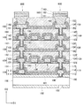
図1は、本発明の第1実施形態に係る多層配線構造体の断面図である。図1では、多層配線構造体の一例として、6層の配線構造体の断面図を用いて説明する。
[Structure of multi-layer wiring structure]
FIG. 1 is a cross-sectional view of a multilayer wiring structure according to a first embodiment of the present invention. In FIG. 1, as an example of the multi-layer wiring structure, a cross-sectional view of the 6-layer wiring structure will be described.
図1では、導電性を有する基板100の一方の面に第1乃至第6配線層(110、120、130、140、150、160)と、第1乃至第6配線層の各配線層を隔離する第1乃至第5層間膜(119、129、139、149、159)と、第1乃至第5配線層(110、120、130、140、150)のうち隣接する配線層を接続する第1乃至第4ビア(191、192、193、194)と、を有する多層配線構造が形成されている。ここで、第1乃至第4ビア(191、192、193、194)は、平面視において互いに重畳している。
In FIG. 1, the first to sixth wiring layers (110, 120, 130, 140, 150, 160) and the first to sixth wiring layers are separated from each other on one surface of the
図1では、第1乃至第6配線層はそれぞれ信号線800およびグランド線900を有している。また、基板100と多層配線構造の最下層の配線層である第1配線層110との間には、開口部180を有する絶縁性の中間層101が設けられ、開口部180に基板100とグランド線900の第1配線層110とを接続する導通部190が形成されている。図1では、第1配線層110の一部が開口部180に充填されることで、導通部190を形成する構造を例示したが、この構造に限定されず、例えば、導通部190として、第1配線層110とは異なる導電層を使用してもよい。
In FIG. 1, the first to sixth wiring layers have a
図1では、第1配線層110は第1導電層111および第2導電層112を有する。第2導電層112としては、電気抵抗が低い金属材料が好ましい。例えば、銅(Cu)、銀(Ag)、金(Au)、アルミニウム(Al)などを使用することができる。また、アルミニウム−ネオジウム合金(Al−Nd)やアルミニウム−銅合金(Al−Cu)などのアルミニウム合金を使用することができる。第1導電層111としては、密着性や、第2導電層112に対するバリア性を有する材料を使用することが好ましい。例えば、第2導電層112としてCuを使用した場合、第1導電層111としては、チタン(Ti)、窒化チタン(TiN)、タンタル(Ta)、窒化タンタル(TaN)、Cr(クロム)などを使用することができる。なお、図1では、配線層として2つの導電層の積層構造を例示したが、この構造に限定されず、1つの導電層の単層構造であってもよく、また、3つ以上の導電層による積層構造であってもよい。
In FIG. 1, the
図1では、第1層間膜119は第1無機絶縁層113、第2無機絶縁層114および第1有機絶縁層115を有する。第1無機絶縁層113は、第1導電層111、第2導電層112および露出された中間層101を覆うように形成されている。また、第2無機絶縁層114は第1無機絶縁層113を覆うように形成されており、さらにその上に第1有機絶縁層115が形成されている。ここで、第1有機絶縁層115の誘電率は、第1無機絶縁層113および第2無機絶縁層114の各々の誘電率よりも低いことが望ましい。なお、第1層間膜119は上記3層構造に限るものではなく、有機絶縁層又は無機絶縁層を少なくとも1層以上含むように構成されていてもよい。
In FIG. 1, the
第1無機絶縁層113は、第2導電層112に対するバリア性を有している材料を使用することが好ましい。換言すると、第1無機絶縁層113は、第2無機絶縁層114や第1有機絶縁層115に比べて、第2導電層112の拡散速度が遅い材料であることが好ましい。例えば、第2導電層112としてCuを使用した場合、第1無機絶縁層113としては、窒化シリコン(SiN)、酸化アルミニウム(Al2O3)、窒化アルミニウム(AlN)、シリコンカーバイト(SiC)、窒化シリコンカーバイト(SiCN)、炭素添加シリコンオキサイド(SiOC)などを使用することができる。また、第1無機絶縁層113は被覆性の良い成膜条件で成膜することが好ましい。また、第2導電層112としてCuを使用し、第1無機絶縁層113としてSiNを使用した場合、Cuの拡散防止機能を得るために一定以上の膜厚であることが好ましく、SiNは比誘電率が7.5と高いため配線層間の寄生容量を抑制するために一定以下の膜厚にすることが好ましい。具体的には、SiN膜の膜厚は、好ましくは10nm以上200nm以下であるとよい。また、より好ましくは、50nm以上100nm以下であるとよい。
For the first inorganic insulating
第1無機絶縁層113は、第1配線層110によって形成された段差部において、第1無機絶縁層113のひび割れや、膜が粗な領域が発生しないようにすることが好ましい。例えば、第1無機絶縁層113は、成膜温度が高い条件で成膜することが望ましく、好ましくは200℃以上であるとよい。より好ましくは、300℃以上であるとよい。また、第1無機絶縁層113の被覆性を良くするために、第1配線層110の端面を中間層101の表面に対して傾斜した順テーパ形状にしてもよい。第1配線層110のテーパ角度は、好ましくは30度以上90度以下であるとよい。より好ましくは、30度以上60度以下であるとよい。ここで、第1配線層110に含まれる第1導電層111と第2導電層112の両方が順テーパ形状でなくてもよく、いずれか一方が順テーパ形状であればよい。
The first inorganic insulating
第2無機絶縁層114は、第1無機絶縁層113およびその上に形成される第1有機絶縁層115との密着性がよい材料を使用することが好ましい。例えば、第2無機絶縁層114としては、酸化シリコン(SiO2)、酸化アルミニウム(Al2O3)などを使用することができる。また、第2無機絶縁層114は被覆性の良い成膜条件で成膜することが好ましい。また、SiO2膜は、基板の反りを調整及び信頼性向上のために一定以上の膜厚であることが好ましく、膜厚が厚すぎるとPIの応力との釣り合いが取れなくなるため一定以下の膜厚であることが好ましい。具体的には、SiO2膜の膜厚は、好ましくは1μm以上8μm以下であるとよい。また、より好ましくは2μm以上5μm以下であるとよい。
For the second inorganic insulating
第1有機絶縁層115は、第1配線層110によって形成された段差を緩和または平坦化し、また、誘電率が第1無機絶縁層113および第2無機絶縁層114よりも低い材料であることが好ましく、例えば感光性ポリイミドなどの樹脂材料で形成されるとよい。第1有機絶縁層115の膜厚は、少なくとも第1配線層110によって形成される段差以上の膜厚であることが好ましく、また、配線層間の寄生容量を小さくするために、塗布工程の可能な限り厚く形成することが好ましい。具体的には、第1有機絶縁層の膜厚は、好ましくは4μm以上24μm以下であるとよい。また、より好ましくは8μm以上20μm以下であるとよい。また、感光性ポリイミドの代わりに、感光性アクリルや感光性シロキサンなどを使用することができる。その他にも、誘電率が低く、Cuに対するバリア性を有するベンゾシクロブテンを使用してもよい。また、感光性樹脂に限らず、非感光性樹脂を使用してもよい。
The first organic insulating
非感光性樹脂としては、エポキシ樹脂、ポリイミド樹脂、ベンゾシクロブテン樹脂、ポリアミド、フェノール樹脂、シリコーン樹脂、フッ素樹脂、液晶ポリマー、ポリアミドイミド、ポリベンゾオキサゾール、シアネート樹脂、アラミド、ポリオレフィン、ポリエステル、BTレジン、FR−4、FR−5、ポリアセタール、ポリブチレンテレフタレート、シンジオタクチック・ポリスチレン、ポリフェニレンサルファイド、ポリエーテルエーテルケトン、ポリエーテルニトリル、ポリカーボネート、ポリフェニレンエーテルポリサルホン、ポリエーテルスルホン、ポリアリレート、ポリエーテルイミドなどを用いることができる。上記の樹脂は単体で用いられてもよく、2種類以上の樹脂を組み合わせて用いられてもよい。また、上記の樹脂に、ガラス、タルク、マイカ、シリカ、アルミナ等、無機フィラーを併用して用いてもよい。 Non-photosensitive resins include epoxy resin, polyimide resin, benzocyclobutene resin, polyamide, phenol resin, silicone resin, fluororesin, liquid crystal polymer, polyamideimide, polybenzoxazole, cyanate resin, aramid, polyolefin, polyester, and BT resin. , FR-4, FR-5, Polyacetal, Polybutylene terephthalate, Syndiotactic polystyrene, Polyphenylene sulfide, Polyether ether ketone, Polyethernitrile, Polycarbonate, Polyphenylene ether Polysulfone, Polyethersulfone, Polyarylate, Polyetherimide, etc. Can be used. The above resin may be used alone or in combination of two or more kinds of resins. Further, an inorganic filler such as glass, talc, mica, silica, or alumina may be used in combination with the above resin.
第1層間膜119には、開口部181が設けられており、開口部181の内部には第1ビア191が充填されている。図1では、第2配線層120の一部が開口部181に充填されることで、第1ビア191を形成する構造を例示したが、この構造に限定されず、例えば、第1ビア191として、第2配線層120とは異なる導電層を使用してもよい。また、図1では、開口部181および第1ビア191は基板に対して直角の形状を有する構造を例示したが、この構造に限定されず、開口部181および第1ビア191が基板に対して順テーパ形状を有していてもよく、また、開口部181および第1ビア191が基板に対して逆テーパ形状を有していてもよい。また、図1では、開口部181が導電層で満たされた構造を例示したが、ビアは隣接する配線層間を接続すればよく、開口部181の一部が空洞であってもよい。
The
図1のように、第2配線層120を第1ビア191として使用する場合、第4導電層122として、第2導電層112と同様に電気抵抗が低い銅(Cu)、銀(Ag)、金(Au)、アルミニウム(Al)などを使用することができる。また、アルミニウム−ネオジウム合金(Al−Nd)やアルミニウム−銅合金(Al−Cu)などのアルミニウム合金を使用することができる。また、第3導電層121として、第1導電層111と同様に第4導電層122に対するバリア性を有する材料を使用することが好ましい。例えば、第4導電層122がCuを含む場合、第3導電層121としては、チタン(Ti)、窒化チタン(TiN)、タンタル(Ta)、窒化タンタル(TaN)、Cr(クロム)などを使用することができる。
As shown in FIG. 1, when the
第1ビア191は、その底部において第1配線層110の第2導電層112と接しており、第1配線層110と第2配線層120とが電気的に接続される。なお、図1では、第2配線層126、127は上下の配線層と接続されていないが、図1に示す断面とは異なる箇所で上下の配線層と接続されていてもよい。
The first via 191 is in contact with the second
第2配線層120上には第2層間膜129が形成されている。第2層間膜129は、第1層間膜119と同じ構造を有しており、第3無機絶縁層123、第4無機絶縁層124および第2有機絶縁層125を有する。図1では、第2層間膜129の各々の層に使用される材料は、第1層間膜119の各々の層と同じ材料を使用しているため、ここでは詳細な説明は省略する。ただし、第2層間膜129の各々の層に使用する材料は、第1層間膜119の各々の層と同じ材料に限定されず、その層間膜の目的に応じて適宜選択することができる。
A
以降、第2配線層120と同様にして、第3乃至第5配線層(130、140、150)を形成することができる。第3配線層130の第5導電層131、第4配線層140の第7導電層141、第5配線層150の第9導電層151はそれぞれ第1導電層111と同じ材料で形成することができる。また、第3配線層130の第6導電層132、第4配線層140の第8導電層142、第5配線層150の第10導電層152はそれぞれ第2導電層112と同じ材料で形成することができる。ただし、これらの導電層は、必ずしも第1導電層111または第2導電層112と同じでなくてもよく、その配線層の目的に応じて適宜選択することができる。
After that, the third to fifth wiring layers (130, 140, 150) can be formed in the same manner as the
また、第2層間膜129と同様にして、第3乃至第5層間膜(139、149、159)を形成することができる。第3層間膜139の第5無機絶縁層133、第4層間膜149の第7無機絶縁層143、第5層間膜159の第9無機絶縁層153はそれぞれ第1無機絶縁層113と同じ材料で形成することができる。また、第3層間膜139の第6無機絶縁層134、第4層間膜149の第8無機絶縁層144、第5層間膜159の第10無機絶縁層154はそれぞれ第2無機絶縁層114と同じ材料で形成することができる。また、第3層間膜139の第3有機絶縁層135、第4層間膜149の第4有機絶縁層145、第5層間膜159の第5有機絶縁層155はそれぞれ第1有機絶縁層115と同じ材料で形成することができる。ただし、これらの絶縁層は、必ずしも第1無機絶縁層113、第2無機絶縁層114または第1有機絶縁層115と同じでなくてもよく、その絶縁層の目的に応じて適宜選択することができる。
Further, the third to fifth interlayer films (139, 149, 159) can be formed in the same manner as the
第1乃至第4ビア(191、192、193、194)はそれぞれ同じ平面座標で積層された、いわゆる、スタックビア構造を有している。換言すると、第1乃至第4ビア(191、192、193、194)は平面視において互いに重畳している。ここで、重畳するビアは平面視において完全に重畳する構造に限定されず、例えば、ビアの一部が重畳した構造を含む。図1に示すスタックビア構造において、積層された全てのビアが平面視において互いに重畳した構造を例示したが、この構造に限定されず、少なくともある配線層の上下に形成されたビアが平面視においた互いに重畳していればよい。例えば、第2配線層120の下の第1ビア191と上の第2ビア192とが、平面視において少なくとも一部で重畳していればよい。
The first to fourth vias (191, 192, 193, 194) each have a so-called stack via structure in which they are laminated with the same plane coordinates. In other words, the first to fourth vias (191, 192, 193, 194) overlap each other in a plan view. Here, the overlapping vias are not limited to a structure in which the vias are completely superimposed in a plan view, and include, for example, a structure in which a part of the vias is superimposed. In the stack via structure shown in FIG. 1, a structure in which all the stacked vias are superimposed on each other in a plan view is illustrated, but the structure is not limited to this structure, and at least the vias formed above and below a certain wiring layer are in the plan view. It suffices if they overlap each other. For example, the first via 191 below the
また、図1では、第1乃至第4ビア(191、192、193、194)は全て同じ径である構造を例示したが、この構造に限定されず、層によってビアの径が異なっていてもよい。例えば、下の層のビア(例えば第1ビア191)に比べて、上の層のビア(例えば第4ビア194)の方が径が大きい構造であってもよい。また、特定の層のビアの径が他の層のビアの径と異なる構造であってもよい。 Further, in FIG. 1, a structure in which the first to fourth vias (191, 192, 193, 194) all have the same diameter is illustrated, but the structure is not limited to this, and the diameter of the via may differ depending on the layer. Good. For example, the vias in the upper layer (for example, the fourth via 194) may have a larger diameter than the vias in the lower layer (for example, the first via 191). Further, the diameter of the vias of the specific layer may be different from the diameter of the vias of the other layers.
図1において、第5配線層150は、第5層間膜159に設けられた開口部185を介して、最上層の第6配線層160に接続される。第6配線層160は、第11導電層161、第12導電層162および第13導電層163を有する。第11導電層161としては、電気抵抗が低く、第10導電層152との密着性がよい材料を使用することが好ましい。例えば、第10導電層152と同じ材料を使用するとよく、Cu、Ag、Au、Al、Al−Nd、Al−Cuなどを使用することができる。
In FIG. 1, the
また、第13導電層163としては、耐食性が高く、酸化しにくく、外部素子との接触抵抗が低い材料を使用することが好ましい。例えば、Au、白金(Pt)などを使用することができる。また、第12導電層162としては、第11導電層161および第13導電層163と密着性がよい材料が好ましい。また、例えば、第13導電層163をめっきで形成する場合は、第13導電層163のシード層として適した材料を使用することが好ましい。例えば、Ti、ニッケル(Ni)、TiN、Crなどを使用することができる。
Further, as the thirteenth
上記の多層配線構造と基板との間には、絶縁性の中間層101が形成されている。中間層101は、多層配線構造に起因する応力が基板に伝わることを緩和するために、基板100よりも柔らかい、つまりヤング率が小さいことが望ましい。また、中間層101は、基板の熱膨張が多層配線構造に伝わることを緩和するために、基板100よりも伸縮しやすく、第1配線層110の第1導電層111および第2導電層112よりも伸縮しにくいことが望ましい。つまり、基板100よりも熱膨張率が高く、第1配線層よりも熱膨張率が低いことが望ましい。ここで、第2導電層112の膜厚が、例えば第1導電層111の膜厚に比べて5倍以上厚い場合、熱膨張率に起因する応力は第2導電層112に起因する応力が支配的になるため、中間層101の熱膨張率は第2導電層112の熱膨張率よりも低ければよい。また、中間層101は樹脂材料を含むことが望ましい。また、中間層101は、第2導電層112に対するバリア性を有している材料を使用することが好ましい。換言すると、中間層101は、基板100に比べて、第2導電層112の拡散速度が遅い材料であることが好ましい。例えば、第2導電層112がCuを含む場合、中間層101としては、ポリイミド等の樹脂材料を使用することができる。図1では、多層配線構造と基板との間に1層の中間層が挟まれた構造を例示したが、この構造に限定されず、中間層と多層配線構造、または、中間層と基板との間に他の層が挟まれていてもよい。
An insulating
ここで、図1では、設計の自由度が高い多層配線構造体を提供するため、また、平面方向の占有面積の小さい多層配線構造体を提供するために、複数のビアが平面視において互いに重畳したスタックビア構造が開示されている。プロセス中の熱処理工程による伸縮の度合いは、有機絶縁層と配線層との間、または、有機絶縁層と基板との間で異なる。そのため、スタックビア構造では、配線層およびビアが重畳した領域A−B線と、各配線層間に有機絶縁層が形成された領域C−D線とでは、熱処理工程による伸縮の度合いおよび内部に発生する応力は大きく異なる。 Here, in FIG. 1, a plurality of vias are superimposed on each other in a plan view in order to provide a multilayer wiring structure having a high degree of freedom in design and to provide a multilayer wiring structure having a small occupied area in the plane direction. The stack via structure is disclosed. The degree of expansion and contraction due to the heat treatment step during the process differs between the organic insulating layer and the wiring layer, or between the organic insulating layer and the substrate. Therefore, in the stack via structure, the region AB line on which the wiring layer and vias are superimposed and the region CD line in which the organic insulating layer is formed between the wiring layers are generated in the degree of expansion and contraction due to the heat treatment step and inside. The stress applied is very different.
特に、有機絶縁層に比べて硬い、つまりヤング率が大きい配線層が積層された領域A−B線では、配線層間に有機絶縁層が配置された領域C−D線に比べてD2(立体)方向に大きい応力が発生する。また、有機絶縁層と基板との間にも、熱処理工程による伸縮の度合いに起因したD1(平面)方向の応力が基板全面で発生する。 In particular, in the region AB line where the wiring layers harder than the organic insulating layer, that is, having a large Young's modulus are laminated, D2 (three-dimensional) as compared with the region CD line in which the organic insulating layer is arranged between the wiring layers. A large stress is generated in the direction. Further, stress in the D1 (planar) direction due to the degree of expansion and contraction due to the heat treatment step is also generated on the entire surface of the substrate between the organic insulating layer and the substrate.
従来のように、基板上に中間層を設けずにスタックビア構造を形成すると、上記のD1方向またはD2方向の応力に起因して、ビアや無機絶縁層へのクラック発生や、ビアと配線の剥離などの問題が発生する。しかし、図1に示した構造によると、少なくとも第1配線層110と基板100との間に中間層101が設けられている領域においては、上記のD1方向またはD2方向の応力を緩和することができ、ビアや無機絶縁層へのクラック発生や、ビアと配線の剥離などの問題を抑制することができる。
When a stack via structure is formed without providing an intermediate layer on the substrate as in the conventional case, cracks occur in the vias and the inorganic insulating layer due to the above stress in the D1 direction or the D2 direction, and the vias and the wiring are connected. Problems such as peeling occur. However, according to the structure shown in FIG. 1, the stress in the D1 direction or the D2 direction can be relaxed at least in the region where the
また、従来のように、基板上に中間層を設けずに多層配線構造を形成した構造において、特に第1配線層110の第2導電層112がCuを含む場合、第1導電層111および第1無機絶縁層113としてCuに対するバリア性を有する材料を使用した場合であっても、熱処理工程によって第1無機絶縁層113に発生したクラックを介して、Cuが基板まで拡散することがある。例えば基板100に導電性または半導体の材料を用いた場合、第1配線層110と基板100がショートしてしまう問題が発生する。このような問題が発生すると、少なくとも第1配線層110を信号線に使用することはできず、設計の自由度が制限されてしまう。
Further, in a structure in which a multilayer wiring structure is formed without providing an intermediate layer on a substrate as in the conventional case, particularly when the second
上記のように、基板と多層配線構造との間に上記の特徴を有する絶縁性の中間層を設けることで、熱処理工程によって配線層およびビアが重畳した領域で発生する立体方向の応力を緩和することができる。また、中間層を設けることで、熱処理工程によって基板全面で発生する平面方向の応力も緩和することができる。その結果、ビアや無機絶縁層へのクラック発生や、ビアと配線の剥離などの問題を抑制することができる。 As described above, by providing an insulating intermediate layer having the above characteristics between the substrate and the multilayer wiring structure, the stress in the three-dimensional direction generated in the region where the wiring layer and vias are superimposed by the heat treatment step is relaxed. be able to. Further, by providing the intermediate layer, the stress in the plane direction generated on the entire surface of the substrate by the heat treatment step can be relaxed. As a result, problems such as cracks in the vias and the inorganic insulating layer and peeling of the vias and the wiring can be suppressed.
また、基板と多層配線構造との間に上記の特徴を有する絶縁性の中間層を設けることで、熱処理工程によってCuが基板まで拡散することを抑制することができる。その結果、第1配線層と基板がショートする問題を抑制することができるため、第1配線層110を信号線800に使用することができ、特性インピーダンスを整合させた配線を配置することができる。また、グランド線900を導電性の基板100に接続させることで、より安定したグランド特性を得ることができる。
Further, by providing an insulating intermediate layer having the above characteristics between the substrate and the multilayer wiring structure, it is possible to suppress the diffusion of Cu to the substrate by the heat treatment step. As a result, since the problem that the first wiring layer and the substrate are short-circuited can be suppressed, the
したがって、図1に一例を示した第1実施形態によると、多層配線構造において、設計の自由度が向上する多層配線構造体を提供することができる。また、熱処理工程に対する耐性の高い多層配線構造体を提供することができる。また、スタックビア構造の多層配線構造体を得ることができることから、平面方向の占有面積の小さい多層配線構造体を提供することができる。また、有機絶縁層として、無機絶縁層よりも誘電率が低い材料を使用することで、積層された各配線間の寄生容量を小さくすることができるため、配線を伝達する信号の遅延を抑制することができる多層配線構造体を提供することができる。また、すべての配線層において、特性インピーダンスが整合された配線が配置可能となり、高速伝送を可能とする多層配線構造体を提供することができる。 Therefore, according to the first embodiment shown in FIG. 1 as an example, it is possible to provide a multi-layer wiring structure in which the degree of freedom in design is improved in the multi-layer wiring structure. Further, it is possible to provide a multilayer wiring structure having high resistance to a heat treatment step. Further, since a multi-layer wiring structure having a stack via structure can be obtained, it is possible to provide a multi-layer wiring structure having a small occupied area in the plane direction. Further, by using a material having a dielectric constant lower than that of the inorganic insulating layer as the organic insulating layer, the parasitic capacitance between the laminated wirings can be reduced, so that the delay of the signal transmitted through the wirings is suppressed. It is possible to provide a multilayer wiring structure capable of providing a multilayer wiring structure. Further, wiring having a matching characteristic impedance can be arranged in all the wiring layers, and a multi-layer wiring structure capable of high-speed transmission can be provided.
[多層配線構造体の製造方法]
次に、図2乃至19を用いて、本発明の第1実施形態に係る多層配線構造体の製造方法を説明する。図2乃至19において、図1に示す要素と同じ要素には同じ符号を付した。
[Manufacturing method of multilayer wiring structure]
Next, a method of manufacturing the multilayer wiring structure according to the first embodiment of the present invention will be described with reference to FIGS. 2 to 19. In FIGS. 2 to 19, the same elements as those shown in FIG. 1 are designated by the same reference numerals.
図2は、本発明の第1実施形態に係る多層配線構造体の製造方法において、第1導電材料および下部第2導電材料が形成された基板の断面図である。図2に示すように、シリコン基板などの基板100上に、塗布法を用いて、ポリイミドなどの樹脂材料を用いた絶縁性の中間層101を形成する。次に、フォトマスクを用いて露光をした後に現像を行い、図2に示すように、開口部180を形成する。
FIG. 2 is a cross-sectional view of a substrate on which a first conductive material and a lower second conductive material are formed in the method for manufacturing a multilayer wiring structure according to a first embodiment of the present invention. As shown in FIG. 2, an insulating
次に、図3に示すように、スパッタリング法により、中間層101上および開口部180内部に第1導電材料211を成膜し、その上に下部第2導電材料212を成膜することで、導通部190の一部を形成する。下部第2導電材料212としては、低抵抗なCuを使用することが好ましく、その場合、第1導電材料211としては、Cuに対してバリア性を有するTiを使用することが好ましい。中間層101および第1導電材料211は、基板100にCuが拡散し、第1導電材料211と基板100とがショートすることを抑制するためのバリア層としての役割を果たす。また、下部第2導電材料212は、電解めっき法によりCuを成長させるためのシード層としての役割を果たす。なお、ここでは、Ti以外のバリア層の材料として、TiNや高融点金属のTa、TaN、Crなどを用いることも可能である。
Next, as shown in FIG. 3, a first
次に、図4に示すように、下部第2導電材料212の上にフォトレジストを塗布した後に、露光及び現像を行うことにより配線形成用レジストパターン310を形成する。その後、電解めっき法を用いて配線形成用レジストパターン310より露出している下部第2導電材料212上に下部第2導電材料212と同じ材料を成長させることで、図5に示すように上部第2導電材料213を形成する。これらの工程によって、開口部180内に導通部190を充填する。図5では、上部第2導電材料213として、下部第2導電材料212と同じ材料を成長させる製造方法を例示したが、この方法に限定されず、上部第2導電材料213を下部第2導電材料212と異なる材料を成長させてもよい。
Next, as shown in FIG. 4, the
次に、上部第2導電材料213を形成した後に、配線形成用レジストパターン310を形成するフォトレジストを有機溶媒により除去し、図6の構造を得る。なお、フォトレジストの除去には、有機溶媒を用いる代わりに、酸素プラズマによるアッシングを用いることもできる。
Next, after forming the upper second
次に、図7に示すように、配線形成用レジストパターン310により覆われていた下部第2導電材料212の一部および第1導電材料211の一部を、酸性の薬液によってエッチングし、第1導電層111および第2導電層112を形成する。このエッチングによって、上部第2導電材料213の膜厚は薄くなるため、この薄膜化の影響を考慮して上部第2導電材料213の膜厚を設定することが好ましい。また、上記の薬液によるエッチングの代わりに、イオンミリングやドライエッチングなどを用いることもできる。
Next, as shown in FIG. 7, a part of the lower second
酸性の水溶液を用いる場合、第2導電層112よりも第1導電層111の方がエッチング速度が速いと、図20に示すようにアンダーカット301が形成されてしまう。特に、配線の幅が5μm以下になると、第1導電層111と下地の中間層101との間での十分な密着性が取れなくなり、第1導電層111が自身の応力などによって剥離してしまうことがある。一方、イオンミリングやドライエッチングを用いる場合には、このようなアンダーカットが起こり難いので、微細な配線形成が可能となる。
When an acidic aqueous solution is used, if the etching rate of the first
次に、図8に示すように、第2導電層112の上にプラズマCVD法を用いて、SiN膜などの第1無機絶縁層113およびSiO2膜などの第2無機絶縁層114を成膜する。SiN膜の成膜には、SiH4をSi源とし、NH3を窒素源として使用することができる。また、SiO2膜の成膜には、SiH4をSi源とし、N2Oを酸素源とすることができる。また、Si源としてテトラエトキシシラン(TEOS)を用いることができる。また、酸素源として、O2を用いることもできる。
Next, as shown in FIG. 8, a first inorganic insulating
SiO2膜は、基板100の反りを抑制する点で、膜応力を−300MPa以上、−100MPa以下の圧縮応力に調整することが好ましい。特に膜応力は−200MPa以上、−150MPa以下に調整することが好ましい。
The SiO 2 film preferably adjusts the film stress to a compressive stress of −300 MPa or more and −100 MPa or less in terms of suppressing warpage of the
なお、第2導電層112がCuを含む場合、Cuの表面に酸化銅が存在すると、第1無機絶縁層113とCuとの密着力が低下するので第1無機絶縁層113の成膜前にCu表面を希硫酸などで洗浄するのが好ましい。また、第1無機絶縁層113の成膜前に同一チャンバ内でCu表面をNH3プラズマに晒して酸化銅の除去を行うこともできる。
When the second
また、第2導電層112がCuを含む場合、第1無機絶縁層113としてはCuに対するバリア性を有するSiN膜を使用することが好ましく、第2導電層112のCu原子やCu分子、Cuイオンが第2導電層112の側面および上面から第2無機絶縁層114に熱拡散するのを防止し、さらに、隣接する配線層間の電界に起因する拡散を防止するバリア絶縁層としての役割を果たす。ここで、SiN膜をバリア絶縁層として用いる代わりに、SiC膜(酸素を数%から10%含んでいてもよい)を用いることができる。SiC膜もプラズマCVDにより成膜することが可能であり、第2導電層112のCu原子やCu分子、Cuイオンの拡散を防止する効果がある。
When the second
また、第2無機絶縁層114としてSiO2膜の代わりに、SiOC膜、SiOF膜などを用いてもよい。SiOC膜やSiOF膜もプラズマCVDによって成膜することができる。SiOC膜やSiOF膜はSiO2膜よりも誘電率が低く、積層された各配線間の寄生容量を小さくすることができる。
Further, as the second inorganic insulating
次に、第2無機絶縁層114の上にスピンコート法によりポリイミドなどの第1有機絶縁層115を塗布する。ポリイミドの代わりに、ベンゾシクロブテンなどを使用してもよい。また、感光性樹脂に限らず、非感光性樹脂を使用してもよい。
Next, the first organic insulating
非感光性樹脂としては、エポキシ樹脂、ポリイミド樹脂、ベンゾシクロブテン樹脂、ポリアミド、フェノール樹脂、シリコーン樹脂、フッ素樹脂、液晶ポリマー、ポリアミドイミド、ポリベンゾオキサゾール、シアネート樹脂、アラミド、ポリオレフィン、ポリエステル、BTレジン、FR−4、FR−5、ポリアセタール、ポリブチレンテレフタレート、シンジオタクチック・ポリスチレン、ポリフェニレンサルファイド、ポリエーテルエーテルケトン、ポリエーテルニトリル、ポリカーボネート、ポリフェニレンエーテルポリサルホン、ポリエーテルスルホン、ポリアリレート、ポリエーテルイミドなどを用いることができる。上記の樹脂は単体で用いられてもよく、2種類以上の樹脂を組み合わせて用いられてもよい。また、上記の樹脂に、ガラス、タルク、マイカ、シリカ、アルミナ等、無機フィラーを併用して用いてもよい。 Non-photosensitive resins include epoxy resin, polyimide resin, benzocyclobutene resin, polyamide, phenol resin, silicone resin, fluororesin, liquid crystal polymer, polyamideimide, polybenzoxazole, cyanate resin, aramid, polyolefin, polyester, and BT resin. , FR-4, FR-5, Polyacetal, Polybutylene terephthalate, Syndiotactic polystyrene, Polyphenylene sulfide, Polyether ether ketone, Polyethernitrile, Polycarbonate, Polyphenylene ether Polysulfone, Polyethersulfone, Polyarylate, Polyetherimide, etc. Can be used. The above resin may be used alone or in combination of two or more kinds of resins. Further, an inorganic filler such as glass, talc, mica, silica, or alumina may be used in combination with the above resin.
ただし、非感光性の樹脂を用いる場合には、さらに感光性の樹脂を塗布しリソグラフィーによりパターンニングを行う必要がある。このため、非感光性の樹脂を用いると工程が増加する場合がある。第1実施形態では、第1有機絶縁層115として感光性ポリイミドを使用した製造方法を説明する。
However, when a non-photosensitive resin is used, it is necessary to further apply a photosensitive resin and perform patterning by lithography. Therefore, the number of steps may be increased if a non-photosensitive resin is used. In the first embodiment, a manufacturing method using photosensitive polyimide as the first organic insulating
第1有機絶縁層115を塗布した場合には、フォトマスクを用いて露光をした後に現像を行い、図9に示すように、第2導電層112の上方の必要な位置に凹部281を形成する。ここで、「必要な位置」とは、第2導電層112をそれよりも上層に形成される配線と接続するビアを配置する必要のある位置を指す。
When the first organic insulating
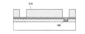
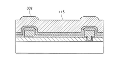
凹部281の形成後に塗布した第1有機絶縁層115を硬化させるために熱硬化処理を行う。熱硬化処理は、使用する有機絶縁層のガラス転移温度以下に設定することが好ましい。ガラス転移温度を越す温度で硬化させると、凹部281の形状が変形してしまい、設計寸法よりも開口径が大きくなるなどの問題が発生するからである。例えば、第1有機絶縁層115としてポリイミドを使用した場合、ポリイミドのガラス転移温度が280℃であれば、250℃で熱処理を行うことが好ましく、例えば、250℃、1時間、窒素雰囲気下で熱処理を行うとよい。なお、熱硬化の処理に限らず、この工程以降の熱処理は、ポリイミドのガラス転移温度を越えないようにして、行うのが好ましい。
A thermosetting treatment is performed to cure the first organic insulating
なお、第1有機絶縁層115を熱硬化させると、第1配線層110による段差の影響で、凹部281以外の領域において、図21に示すような段差302が発生することがある。このような段差は、配線層を積層するにしたがって大きくなり、パターン露光時のフォーカスずれを発生させる。このため、設計寸法に基づく配線パターンの形成が困難となり、隣接する配線がショートする問題や、逆に配線が断線する問題が発生する。このような第1有機絶縁層115の段差302を低減させるために、ポリイミドのような熱収縮率の小さな(好ましくは、熱収縮率が15%以下)有機材料を使用することが好ましい。また、高精度でポリイミドの表面の凹凸を除去するには、フライカッターを用いることもできる。
When the first organic insulating
次に、第1有機絶縁層115をマスクとしてプラズマエッチングすることで、凹部281の底部の第1無機絶縁層113および第2無機絶縁層114をエッチングする。ここでは、第1無機絶縁層113としてSiN膜を使用し、第2無機絶縁層114としてSiO2膜を使用し、第1有機絶縁層115としてポリイミドを使用した場合のエッチング方法について詳しく説明する。
Next, the first inorganic insulating
SiO2膜のエッチングガスとしては、CF4(流量20sccm)とH2(流量5sccm)との混合ガスを用いることができる。混合ガスの流量比を変化させることで、硬化したポリイミドとSiO2膜のエッチング速度の比率を調整することが可能である。ここで、SiO2膜に対するポリイミドのエッチング速度の比率が小さくなるように調整することが好ましい。なお、エッチングガスは、上述したものに限らず、CF4の代わりにCHF3やCH2F2を用いることができる。 As the etching gas for the SiO 2 film, a mixed gas of CF 4 (flow rate 20 sccm) and H 2 (flow rate 5 sccm) can be used. By changing the flow rate ratio of the mixed gas, it is possible to adjust the ratio of the etching rate of the cured polyimide and the SiO 2 film. Here, it is preferable to adjust so that the ratio of the etching rate of polyimide to the SiO 2 film is small. The etching gas is not limited to the one described above, and CHF 3 or CH 2 F 2 can be used instead of CF 4 .
SiN膜のエッチングガスとしては、CF4(流量20sccm)とO2(流量2sccm)との混合ガスを用いることができる。SiN膜のエッチングにおいても、混合ガスの流量比を変化させることで、硬化したポリイミドとSiN膜のエッチング速度の比率を調整することが可能である。SiO2と同様に、SiN膜に対するポリイミドのエッチング速度の比率が小さくなるように調整することが好ましい。 As the etching gas for the SiN film, a mixed gas of CF 4 (flow rate 20 sccm) and O 2 (flow rate 2 sccm) can be used. Also in the etching of the SiN film, it is possible to adjust the ratio of the etching rate of the cured polyimide and the SiN film by changing the flow rate ratio of the mixed gas. Similar to SiO 2 , it is preferable to adjust so that the ratio of the etching rate of polyimide to the SiN film is small.
上記のように、第1無機絶縁層113および第2無機絶縁層114のエッチングによって、第1配線層110と第2配線層120とを電気的に接続する第1ビア191を充填するための開口部181が形成される。この開口部181が形成された直後は、開口部181の側壁や底部にSiやFを含む炭素化合物が付着している場合がある。この炭素化合物を除去するために、有機溶剤で洗浄を行ってもよい。また、開口部181の底部において露出した第2導電層112の表面はプラズマエッチングによって酸化している場合がある。この表面の酸化物を除去するために、希硫酸による洗浄を行ってもよい。
As described above, the opening for filling the first via 191 that electrically connects the
第1無機絶縁層113および第2無機絶縁層114に対するプラズマエッチングにより、第1有機絶縁層115の表面はプラズマダメージを受け、第1有機絶縁層115固有の耐熱性が損なわれている場合がある。この場合には、例えば第1有機絶縁層115のガラス転移温度以下で熱処理を行うことで、表面のダメージ層を除去することができる。このようにして、図10に示す構造を得ることができる。
Due to plasma etching on the first inorganic insulating
次に、図11に示すように、スパッタリング法によって第3導電材料221を成膜する。第2導電層112がCuを含む場合、第3導電材料221としては、第1導電層111と同様にTi、TiN、Ta、TaN、Crなどを使用することで、Cu原子やCu分子、Cuイオンが拡散しないようにするバリアメタルとして機能させることができる。
Next, as shown in FIG. 11, the third
次に、図12に示すように、スパッタリング法によって下部第4導電材料222を成膜する。下部第4導電材料222としては、低抵抗なCuを使用することが好ましい。また、下部第4導電材料222は、電解めっき法によりCuを成長させるためのシード層としての役割を果たす。
Next, as shown in FIG. 12, the lower fourth
次に、図13に示すように、下部第4導電材料222の上にフォトレジストを塗布した後に、露光及び現像を行うことにより配線形成用レジストパターン320を形成する。その後、電解めっき法を用いて配線形成用レジストパターン320より露出している下部第4導電材料222上に下部第4導電材料222と同じ材料を成長させることで、図14に示すように上部第4導電材料223を形成する。図14では、上部第4導電材料223として、下部第4導電材料222と同じ材料を成長させる製造方法を例示したが、この方法に限定されず、上部第4導電材料223を下部第4導電材料222と異なる材料を成長させてもよい。
Next, as shown in FIG. 13, a photoresist is applied on the lower fourth
次に、上部第4導電材料223を形成した後に、配線形成用レジストパターン320を形成するフォトレジストを有機溶媒により除去し、図15の構造を得る。なお、フォトレジストの除去には、有機溶媒を用いる代わりに、酸素プラズマによるアッシングを用いることもできる。
Next, after forming the upper fourth
次に、図16に示すように、配線形成用レジストパターン320により覆われていた下部第4導電材料222の一部および第3導電材料221の一部を、酸性の薬液によってエッチングし、第3導電層121および第4導電層122を形成する。このエッチングによって、上部第4導電材料223の膜厚は薄くなるため、この薄膜化の影響を考慮して上部第4導電材料223の膜厚を設定することが好ましい。また、上記の薬液によるエッチングの代わりに、イオンミリングやドライエッチングなどを用いることもできる。
Next, as shown in FIG. 16, a part of the lower fourth
次に、図17に示すように、第4導電層122の上に第3無機絶縁層123および第4無機絶縁層124を成膜する。例えば、第4導電層122がCuを含む場合、第3無機絶縁層123としては、第1無機絶縁層113と同様にCuに対するバリア性を有するSiN膜を使用することが好ましく、第4無機絶縁層124としては、第2無機絶縁層114と同様にSiO2膜を使用することが好ましい。第3無機絶縁層123としてSiN膜をバリア絶縁層として用いる代わりに、SiC膜(酸素を数%から10%含んでいてもよい)を用いることができる。また、第4無機絶縁層124としてSiO2膜の代わりに、SiOC膜、SiOF膜などを用いてもよい。
Next, as shown in FIG. 17, a third inorganic insulating
次に、第4無機絶縁層124の上にスピンコート法によりポリイミドなどの第2有機絶縁層125を塗布する。ポリイミドの代わりに、ベンゾシクロブテンなどを使用してもよい。また、感光性樹脂に限らず、非感光性樹脂を使用してもよい。
Next, a second organic insulating
非感光性樹脂としては、エポキシ樹脂、ポリイミド樹脂、ベンゾシクロブテン樹脂、ポリアミド、フェノール樹脂、シリコーン樹脂、フッ素樹脂、液晶ポリマー、ポリアミドイミド、ポリベンゾオキサゾール、シアネート樹脂、アラミド、ポリオレフィン、ポリエステル、BTレジン、FR−4、FR−5、ポリアセタール、ポリブチレンテレフタレート、シンジオタクチック・ポリスチレン、ポリフェニレンサルファイド、ポリエーテルエーテルケトン、ポリエーテルニトリル、ポリカーボネート、ポリフェニレンエーテルポリサルホン、ポリエーテルスルホン、ポリアリレート、ポリエーテルイミドなどを用いることができる。上記の樹脂は単体で用いられてもよく、2種類以上の樹脂を組み合わせて用いられてもよい。また、上記の樹脂に、ガラス、タルク、マイカ、シリカ、アルミナ等、無機フィラーを併用して用いてもよい。 Non-photosensitive resins include epoxy resin, polyimide resin, benzocyclobutene resin, polyamide, phenol resin, silicone resin, fluororesin, liquid crystal polymer, polyamideimide, polybenzoxazole, cyanate resin, aramid, polyolefin, polyester, and BT resin. , FR-4, FR-5, Polyacetal, Polybutylene terephthalate, Syndiotactic polystyrene, Polyphenylene sulfide, Polyether ether ketone, Polyethernitrile, Polycarbonate, Polyphenylene ether Polysulfone, Polyethersulfone, Polyarylate, Polyetherimide, etc. Can be used. The above resin may be used alone or in combination of two or more kinds of resins. Further, an inorganic filler such as glass, talc, mica, silica, or alumina may be used in combination with the above resin.
第1実施形態では、第2有機絶縁層125として感光性ポリイミドを使用した製造方法を説明する。
In the first embodiment, a manufacturing method using photosensitive polyimide as the second organic insulating
第2有機絶縁層125を塗布した場合には、フォトマスクを用いて露光をした後に現像を行い、図18に示すように、第4導電層122の上方の必要な位置に凹部282を形成する。ここで、「必要な位置」とは、第4導電層122をそれよりも上層に形成される配線と接続するビアを配置する必要のある位置を指す。
When the second organic insulating
凹部281の形成後に、第2有機絶縁層125を硬化させるため、第2有機絶縁層125のガラス転移温度以下の温度で熱硬化処理を行う。例えば、第2有機絶縁層125としてポリイミドを使用した場合、ポリイミドのガラス転移温度が280℃であれば、上述のように250℃とする。なお、熱硬化の処理に限らず、この工程以降の熱処理は、ポリイミドのガラス転移温度を越えないようにして、行うのが好ましい。
After forming the
次に、第2有機絶縁層125をマスクとしてプラズマエッチングすることで、凹部282の底部の第3無機絶縁層123および第4無機絶縁層124をエッチングする。プラズマエッチングの方法は、第1無機絶縁層113および第2無機絶縁層114のエッチング方法と同様の方法を使用することができる。第3無機絶縁層123および第4無機絶縁層124のエッチングによって、第2配線層120と第3配線層130とを電気的に接続する第2ビア192を充填するための開口部182が形成される。このようにして、図19に示す構造を得ることができる。
Next, the third inorganic insulating
以降、図11乃至19で説明した方法を繰り返すことで、図1に示す多層配線構造体を得ることができる。 Hereinafter, by repeating the methods described with reference to FIGS. 11 to 19, the multilayer wiring structure shown in FIG. 1 can be obtained.
<第2実施形態>
以下、本発明の第2実施形態に係る多層配線構造体について、図面を参照しながら詳細に説明する。図22は、本発明の第2実施形態に係る多層配線構造体の断面図である。図22は、基板100の一方の面に多層配線構造が形成される点においては図1と類似しているが、基板100の他方の面にパターニングされた裏面絶縁層102を有する点において、図1とは異なる。
<Second Embodiment>
Hereinafter, the multilayer wiring structure according to the second embodiment of the present invention will be described in detail with reference to the drawings. FIG. 22 is a cross-sectional view of the multilayer wiring structure according to the second embodiment of the present invention. FIG. 22 is similar to FIG. 1 in that a multilayer wiring structure is formed on one surface of the
裏面絶縁層102は、平面視において、中間層101に形成された開口部180と同じ平面座標に開口部103を有している。換言すると、中間層101に形成された開口部180または導通部190と、裏面絶縁層102に形成された開口部103とは、平面視において互いに重畳している。裏面絶縁層102は中間層101と同じ材料であってもよく、例えばポリイミド等の樹脂材料を使用することができる。また、裏面絶縁層102の平面形状は開口部180と同様の形状(例えば、ドット状)であってもよい。
The back
上記の構造によれば、熱処理工程によって多層配線構造および中間層101に発生する応力による基板の歪みを緩和することができる。さらに、裏面絶縁層102が、平面視において開口部180と重畳するように開口部103が配置されることで、中間層101によって発生する応力をより効果的に緩和することができる。その結果、基板の歪みが抑制された多層配線構造体を提供することができる。また、基板100は、裏面絶縁層102に形成された開口部103を介して外部の接地部材に接続することができ、より安定したグランド特性を得ることができる。
According to the above structure, it is possible to alleviate the distortion of the substrate due to the stress generated in the multilayer wiring structure and the
<第3実施形態>
以下、本発明の第3実施形態に係る多層配線構造体について、図面を参照しながら詳細に説明する。図23は、本発明の第3実施形態に係る多層配線構造体の断面図である。図23は、図1と類似しているが、中間層101に形成された開口部180および導通部190が、その上層に形成される複数のビアと異なる平面座標に配置される点において、図1とは異なる。換言すると、導通部190と第1乃至第4ビア(191、192、193、194)とは、平面視において互いに異なる位置に配置されている。また、換言すると、少なくとも、導通部190と第1ビア191とは平面視において互いに異なる位置に配置されている。また、換言すると、導通部190と第1ビア191とはクランク構造である。
<Third Embodiment>
Hereinafter, the multilayer wiring structure according to the third embodiment of the present invention will be described in detail with reference to the drawings. FIG. 23 is a cross-sectional view of the multilayer wiring structure according to the third embodiment of the present invention. FIG. 23 is similar to FIG. 1 in that the
上記の構造によれば、グランド線900のスタックビア構造においても、熱処理工程によって発生する立体方向の応力を中間層101によって緩和することができる。その結果、グランド線900付近においても、ビアや無機絶縁層へのクラック発生や、ビアと配線の剥離などの問題を抑制することができる。
According to the above structure, even in the stack via structure of the
<第4実施形態>
以下、本発明の第4実施形態に係る多層配線構造体について、図面を参照しながら詳細に説明する。図24は、本発明の第4実施形態に係る多層配線構造体の断面図である。図24は、基板100の一方の面に多層配線構造が形成される点においては図23と類似しているが、基板100の他方の面にパターニングされた裏面絶縁層102を有する点において、図23とは異なる。
<Fourth Embodiment>
Hereinafter, the multilayer wiring structure according to the fourth embodiment of the present invention will be described in detail with reference to the drawings. FIG. 24 is a cross-sectional view of the multilayer wiring structure according to the fourth embodiment of the present invention. FIG. 24 is similar to FIG. 23 in that a multilayer wiring structure is formed on one surface of the
裏面絶縁層102は、平面視において、積層された複数のビアおよび中間層101に形成された開口部180と同じ平面座標に開口部103を有している。換言すると、複数のビアおよび開口部180と、裏面絶縁層102に形成された開口部103とは、平面視において互いに重畳している。裏面絶縁層102は中間層101と同じ材料であってもよく、例えばポリイミド等の樹脂材料を使用することができる。また、裏面絶縁層102の平面形状は中間層101の開口部180や多層配線構造の開口部181乃至184と同様の形状(例えば、ドット状)であってもよい。
The back
また、図25は、本発明の第4実施形態の変形例に係る多層配線構造体の断面図である。図25は、積層された複数のビアが異なる平面座標に配置されている点において、図24と異なる。換言すると、図25では、積層された複数のビアが平面視において互いに異なる位置に配置されている。また、換言すると、積層された複数のビアはクランク構造を有している。また、図25では、裏面絶縁層102には複数のビアおよび開口部180と平面視において重畳するように開口部103が設けられた構造を例示するが、この構造に限定されず、少なくとも一箇所に基板100との導通を取ることができる開口部を有していればよい。
Further, FIG. 25 is a cross-sectional view of a multilayer wiring structure according to a modified example of the fourth embodiment of the present invention. FIG. 25 differs from FIG. 24 in that the plurality of stacked vias are arranged at different plane coordinates. In other words, in FIG. 25, a plurality of stacked vias are arranged at different positions in a plan view. In other words, the plurality of laminated vias have a crank structure. Further, FIG. 25 illustrates a structure in which the back
上記の構造によれば、熱処理工程によって多層配線構造および中間層101に発生する応力による基板の歪みを緩和することができる。さらに、平面視において中間層101の開口部180および多層配線構造の開口部181乃至184と重畳するように裏面絶縁層102に開口部103が配置されることで、裏面絶縁層102が中間層101および多層配線構造の複数の層間膜(119、129、139、149、159)によって発生する応力をより効果的に緩和することができる。その結果、基板の歪みが抑制された多層配線構造体を提供することができる。また、基板100は、裏面絶縁層102に形成された開口部103を介して外部の接地部材に接続することができ、より安定したグランド特性を得ることができる。
According to the above structure, it is possible to alleviate the distortion of the substrate due to the stress generated in the multilayer wiring structure and the
<第5実施形態>
以下、本発明の第5実施形態に係る多層配線構造体について、図面を参照しながら詳細に説明する。図26は、本発明の第5実施形態に係る多層配線構造体の断面図である。図26は、図1と類似しているが、基板100と中間層101との間にグランド補助層104を有する点において、図1とは異なる。グランド補助層104は、少なくとも導電性の基板100よりも固有抵抗が低く、さらに導通部190との接触抵抗が低い材料が好ましい。つまり、グランド補助層104は金属層であることが好ましい。
<Fifth Embodiment>
Hereinafter, the multilayer wiring structure according to the fifth embodiment of the present invention will be described in detail with reference to the drawings. FIG. 26 is a cross-sectional view of the multilayer wiring structure according to the fifth embodiment of the present invention. FIG. 26 is similar to FIG. 1, but differs from FIG. 1 in that a ground
上記の構造によれば、導通部190と基板100との接触抵抗をより低抵抗化することができる。また、基板100に複数の導通部190を介して複数のグランド線が接続された場合に、複数のグランド線同士を低抵抗で接続することができる。したがって、さらに安定したグランド特性を得ることができる。
According to the above structure, the contact resistance between the
以下、本発明を図27に示す実施例1に基づいて具体的に説明するが、本発明はこれらの実施例のみに限定されるものではない。図27は、本発明の実施例1に係る多層配線構造体の断面図である。実施例1では、第1実施形態の多層配線構造体に対して、さらに2層の配線層を追加して、8層の配線構造体を作製した例について説明する。 Hereinafter, the present invention will be specifically described with reference to Example 1 shown in FIG. 27, but the present invention is not limited to these Examples. FIG. 27 is a cross-sectional view of the multilayer wiring structure according to the first embodiment of the present invention. In the first embodiment, an example in which an eight-layer wiring structure is produced by adding two wiring layers to the multilayer wiring structure of the first embodiment will be described.
まず、基板100として、厚さ400μmのシリコン基板を用意した。次に、基板100上に絶縁性の中間層101として、スピンコート法によって10μmの感光性ポリイミドを塗布し、フォトマスクを用いて露光をした後に現像を行い、直径20μmの開口部180を有する中間層101を形成する。ポリイミドのヤング率は3乃至3.5GPaであり、シリコン基板のヤング率は約185GPaである。つまり、中間層101は基板100よりもヤング率が低い。換言すると、中間層101は基板100よりも柔らかい。また、ポリイミドは後述する配線層に使用するCuに対するバリア性を有している。つまり、ポリイミドはシリコン基板に比べてCuの拡散速度が遅い。
First, as the
中間層101上および開口部180内部には、第1配線層110および導通部190が同一の工程で形成される。第1配線層110および導通部190は、第1導電層111として厚さ50nmのTiと、第2導電層112として厚さ4μmのCuと、の積層で形成する。ここで、第1導電層111のTiは第2導電層112のCuに対するバリア性を有している。開口部180内部は、第1導電層のTiで覆われており、第2導電層のCuと中間層101の開口部180内部とを隔離するように形成されている。また、第1配線層110の配線パターンは線幅は10乃至100μmで形成することができる。
The
図27に示す実施例1では、第2乃至第7配線層(120、130、140、150、160、170)も第1配線層110と同様の積層構造及びパターン線幅で形成される。つまり、第3、5、7、9、11、13導電層(121、131、141、151、161、171)は第1導電層111と同じTiで形成され、第4、6、8、10、12、14導電層(122、132、142、152、162、172)は第2導電層112と同じCuで形成される。
In Example 1 shown in FIG. 27, the second to seventh wiring layers (120, 130, 140, 150, 160, 170) are also formed with the same laminated structure and pattern line width as the
中間層101上に第1配線層110が形成されると、これらを覆って第1層間膜119が形成される。第1層間膜119は、第1無機絶縁層113として厚さ10nmのSiN膜と、第2無機絶縁層114として厚さ2μmのSiO2膜と、第1有機絶縁層115として厚さ12μmのポリイミドと、の積層で形成する。ここで、第1無機絶縁層113のSiN膜および第2無機絶縁層114のSiO2膜はプラズマCVD法を用いて形成される。また、第1有機絶縁層115のポリイミドは、第1配線層110によって形成された段差を緩和または平坦化する。つまり、第1配線層110上の第1有機絶縁層115のポリイミド膜厚115bは、第1配線層110が存在しない、中間層101上の第1有機絶縁層115のポリイミド膜厚115aに比べると薄く形成されることになる。図27に示す実施例1では、膜厚115aは12μmであり、膜厚115bはおおよそ第1配線層110の膜厚の分だけ薄い8μmであった。
When the
続いて、第1層間膜119に開口部181を形成する。開口部181は直径が15μmである。開口部181は、まず、第1有機絶縁層115として感光性ポリイミドを塗布し、フォトマスクを用いて露光をした後に現像を行い、開口部181を設ける位置に、下層の第2無機絶縁層114を露出する凹部を形成する。第1有機絶縁層115の感光性ポリイミドをマスクとして、凹部において露出された第2無機絶縁層114およびその下層の第1無機絶縁層113をプラズマエッチングすることで形成した。第2無機絶縁層114のSiO2膜のエッチングには、CF4(流量20sccm)とH2(流量5sccm)との混合ガスを用いた。また、第1無機絶縁層113のSiN膜のエッチングには、CF4(流量20sccm)とO2(流量2sccm)との混合ガスを用いた。
Subsequently, an
続いて、第1層間膜119上および開口部181内部に第2配線層120および第1ビア191が同一の工程で形成される。第2配線層120および第1ビア191は、第1配線層110と同様に、第3導電層121として厚さ50nmのTiと、第4導電層122として厚さ4μmのCuと、の積層で形成する。ここで、第3導電層121のTiは第4導電層122のCuに対するバリア性を有している。開口部181内部は、第3導電層121のTiで覆われており、第4導電層122のCuと第1層間膜119の開口部181内部とを隔離するように形成されている。
Subsequently, the
第1ビア191の直径191aは開口部181の直径と同じ15μmであり、第1ビア191の上部に位置するランドの直径191bは30μmである。また、隣接するビアの中心間の距離を示すビアピッチは、最もピッチが小さいところで40μmである。
The
上記のようにして、第1配線層、第1層間膜、第1ビアを形成する。これらと同様に第2乃至第7の配線層、層間膜、および第2乃至第6のビアが形成される。そして、第7層間膜179上および第7層間膜179に設けられた開口部187内部に、最上層の第8配線層380および第7ビア197が同一の工程で形成される。第8配線層380は、第15導電層381として厚さ3μmのCuと、第16導電層382として厚さ1μmのNiと、第17導電層383として厚さ1μmのAuと、の積層で形成される。
As described above, the first wiring layer, the first interlayer film, and the first via are formed. Similar to these, the second to seventh wiring layers, interlayer films, and second to sixth vias are formed. Then, the
以上のように、実施例1によれば、基板と多層配線構造との間に、上記の特徴を有する絶縁性の中間層を設けることで、熱処理工程によってCuが基板まで拡散することを抑制することができる。その結果、第1配線層と基板がショートする問題を抑制することができるため、第1配線層110を信号線800に使用することができ、特性インピーダンスを整合させた配線を配置することができる。また、グランド線900を導電性の基板100に接続させることで、より安定したグランド特性を得ることができる。
As described above, according to the first embodiment, by providing an insulating intermediate layer having the above-mentioned characteristics between the substrate and the multilayer wiring structure, it is possible to prevent Cu from diffusing to the substrate by the heat treatment step. be able to. As a result, since the problem that the first wiring layer and the substrate are short-circuited can be suppressed, the
なお、本発明は上記の実施形態に限られたものではなく、趣旨を逸脱しない範囲で適宜変更することが可能である。 The present invention is not limited to the above embodiment, and can be appropriately modified without departing from the spirit.
100:基板
101:中間層
102:裏面絶縁層
103:開口部
104:グランド補助層
110:第1配線層
111:第1導電層
112:第2導電層
113:第1無機絶縁層
114:第2無機絶縁層
115:第1有機絶縁層
119:第1層間膜
120、126、127:第2配線層
121:第3導電層
122:第4導電層
123:第3無機絶縁層
124:第4無機絶縁層
125:第2有機絶縁層
129:第2層間膜
130:第3配線層
131:第5導電層
132:第6導電層
133:第5無機絶縁層
134:第6無機絶縁層
135:第3有機絶縁層
139:第3層間膜
140:第4配線層
141:第7導電層
142:第8導電層
143:第7無機絶縁層
144:第8無機絶縁層
145:第4有機絶縁層
149:第4層間膜
150:第5配線層
151:第9導電層
152:第10導電層
153:第9無機絶縁層
154:第10無機絶縁層
155:第5有機絶縁層
159:第5層間膜
160:第6配線層
161:第11導電層
162:第12導電層
163:第13導電層
180、181、182、185:開口部
190:導通部
191:第1ビア
192:第2ビア
193:第3ビア
194:第4ビア
211:第1導電材料
212:下部第2導電材料
213:上部第2導電材料
221:第3導電材料
222:下部第4導電材料
223:上部第4導電材料
281、282:凹部
301:アンダーカット
302:段差
310、320:配線形成用レジストパターン
800:信号線
900:グランド線
100: Substrate 101: Intermediate layer 102: Back surface insulating layer 103: Opening 104: Ground auxiliary layer 110: First wiring layer 111: First conductive layer 112: Second conductive layer 113: First inorganic insulating layer 114: Second Inorganic insulating layer 115: First organic insulating layer 119: First interlayer film 120, 126, 127: Second wiring layer 121: Third conductive layer 122: Fourth conductive layer 123: Third inorganic insulating layer 124: Fourth inorganic Insulating layer 125: Second organic insulating layer 129: Second interlayer film 130: Third wiring layer 131: Fifth conductive layer 132: Sixth conductive layer 133: Fifth inorganic insulating layer 134: Sixth inorganic insulating layer 135: Third 3 Organic insulating layer 139: 3rd interlayer film 140: 4th wiring layer 141: 7th conductive layer 142: 8th conductive layer 143: 7th inorganic insulating layer 144: 8th inorganic insulating layer 145: 4th organic insulating layer 149 : 4th interlayer film 150: 5th wiring layer 151: 9th conductive layer 152: 10th conductive layer 153: 9th inorganic insulating layer 154: 10th inorganic insulating layer 155: 5th organic insulating layer 159: 5th interlayer film 160: 6th wiring layer 161: 11th conductive layer 162: 12th conductive layer 163: 13th conductive layer 180, 181, 182, 185: opening 190: conductive portion 191: 1st via 192: 2nd via 193: 3rd via 194: 4th via 211: 1st conductive material 212: Lower 2nd conductive material 213: Upper 2nd conductive material 221: 3rd conductive material 222: Lower 4th conductive material 223: Upper 4th conductive material 281 282: Recessed 301: Undercut 302: Step 310, 320: Conducting pattern for wiring formation 800: Signal line 900: Ground line
Claims (8)
前記導電性を有する層の一方の面に複数の配線層が積層された多層配線構造と、を有し、
前記多層配線構造は、隣接する配線層を接続し、平面視において互いに重畳する複数の第1のビアと平面視において互いに重畳する複数の第2のビアを含み、
前記複数の第1のビアのうちの一つと前記複数の第2のビアのうちの一つはクランク構造を形成し、
前記複数の配線層のうち少なくとも一つの配線層は、グランド線を含み、
前記多層配線構造と前記導電性を有する層との間に、第1の開口部を有する絶縁性の中間層が、前記導電性を有する層の一方の面に直接設けられ、
前記第1の開口部に前記導電性を有する層および前記グランド線を接続する導通部が設けられ、
前記導電性を有する層の他方の面に絶縁層が設けられ、
前記絶縁層は、第2の1の開口部および第2の2の開口部を有し、
前記第2の1の開口部は、前記複数の第1のビアのうちの一つと重畳し、
前記第2の2の開口部は、前記複数の第2のビアのうちの一つと重畳していることを特徴とする多層配線構造体。 With a conductive layer
It has a multi-layer wiring structure in which a plurality of wiring layers are laminated on one surface of the conductive layer.
The multilayer wiring structure includes a plurality of first vias that connect adjacent wiring layers and overlap each other in a plan view and a plurality of second vias that overlap each other in a plan view .
One of the plurality of first vias and one of the plurality of second vias form a crank structure.
At least one wiring layer of the plurality of wiring layers includes a ground line,
Wherein between the layer having a multilayer wiring structure of the conductive, insulating intermediate layer having a first opening is provided directly on one surface of the layer having the conductivity,
Conducting portion is provided to connect the layers and the ground line with the conductive to the first opening,
An insulating layer is provided on the other surface of the conductive layer.
The insulating layer has a second opening and a second opening.
The second 1 opening overlaps with one of the plurality of first vias.
A multilayer wiring structure characterized in that the second second opening is superimposed on one of the plurality of second vias .
Priority Applications (1)
| Application Number | Priority Date | Filing Date | Title |
|---|---|---|---|
| JP2019114662A JP6766923B2 (en) | 2019-06-20 | 2019-06-20 | Multi-layer wiring structure |
Applications Claiming Priority (1)
| Application Number | Priority Date | Filing Date | Title |
|---|---|---|---|
| JP2019114662A JP6766923B2 (en) | 2019-06-20 | 2019-06-20 | Multi-layer wiring structure |
Related Parent Applications (1)
| Application Number | Title | Priority Date | Filing Date |
|---|---|---|---|
| JP2018085383A Division JP6544462B2 (en) | 2018-04-26 | 2018-04-26 | Multilayer wiring structure |
Publications (3)
| Publication Number | Publication Date |
|---|---|
| JP2019153818A JP2019153818A (en) | 2019-09-12 |
| JP2019153818A5 JP2019153818A5 (en) | 2019-10-24 |
| JP6766923B2 true JP6766923B2 (en) | 2020-10-14 |
Family
ID=67948954
Family Applications (1)
| Application Number | Title | Priority Date | Filing Date |
|---|---|---|---|
| JP2019114662A Active JP6766923B2 (en) | 2019-06-20 | 2019-06-20 | Multi-layer wiring structure |
Country Status (1)
| Country | Link |
|---|---|
| JP (1) | JP6766923B2 (en) |
Family Cites Families (4)
| Publication number | Priority date | Publication date | Assignee | Title |
|---|---|---|---|---|
| JP2002204078A (en) * | 2000-12-28 | 2002-07-19 | Fujitsu Ltd | Multilayer circuit board and semiconductor integrated circuit device |
| JP4340729B2 (en) * | 2002-06-10 | 2009-10-07 | 富士通マイクロエレクトロニクス株式会社 | Semiconductor device and manufacturing method thereof |
| JP4561235B2 (en) * | 2004-08-20 | 2010-10-13 | 富士通株式会社 | Semiconductor device design method |
| JP5413371B2 (en) * | 2008-10-21 | 2014-02-12 | 日本電気株式会社 | Semiconductor device and manufacturing method thereof |
-
2019
- 2019-06-20 JP JP2019114662A patent/JP6766923B2/en active Active
Also Published As
| Publication number | Publication date |
|---|---|
| JP2019153818A (en) | 2019-09-12 |
Similar Documents
| Publication | Publication Date | Title |
|---|---|---|
| JP7452605B2 (en) | Multilayer wiring structure and its manufacturing method | |
| JP2004064046A (en) | Semiconductor device and its manufacturing method | |
| TWI768040B (en) | Semiconductor device and method of manufacturing the same | |
| US8035232B2 (en) | Semiconductor device including interconnects, vias connecting the interconnects and greater thickness of the liner film adjacent the vias | |
| US8173907B2 (en) | Interposer and method for manufacturing interposer | |
| JP5400355B2 (en) | Semiconductor device | |
| US8188378B2 (en) | Interposer and method for manufacturing interposer | |
| JP6766923B2 (en) | Multi-layer wiring structure | |
| WO2014174825A1 (en) | Semiconductor device | |
| JP6330374B2 (en) | Multilayer wiring structure | |
| JP6544462B2 (en) | Multilayer wiring structure | |
| JP2012160595A (en) | Semiconductor device and method of manufacturing the same | |
| JP6536710B2 (en) | Multilayer wiring structure | |
| JP2019117875A (en) | Wiring substrate and semiconductor device having wiring substrate | |
| JP6330373B2 (en) | Multilayer wiring structure | |
| KR100750550B1 (en) | Method for fabricating semiconductor device | |
| JP7390323B2 (en) | Multilayer wiring structure and semiconductor device using multilayer wiring structure | |
| US10332839B2 (en) | Interconnect structure and fabricating method thereof | |
| JP2022110019A (en) | Wiring board and semiconductor device having wiring board | |
| KR100508534B1 (en) | Method for forming an air gap in a semiconductor metal line manufacturing process | |
| KR100668960B1 (en) | Metal line in semiconductor device and fabricating method threof | |
| TW201724437A (en) | Method for forming semiconductor structure | |
| JPH10313052A (en) | Method for forming wiring of semiconductor device and wiring structure | |
| JP2008066451A (en) | Semiconductor device |
Legal Events
| Date | Code | Title | Description |
|---|---|---|---|
| A621 | Written request for application examination |
Free format text: JAPANESE INTERMEDIATE CODE: A621 Effective date: 20190620 |
|
| A521 | Written amendment |
Free format text: JAPANESE INTERMEDIATE CODE: A523 Effective date: 20190829 |
|
| TRDD | Decision of grant or rejection written | ||
| A01 | Written decision to grant a patent or to grant a registration (utility model) |
Free format text: JAPANESE INTERMEDIATE CODE: A01 Effective date: 20200818 |
|
| A61 | First payment of annual fees (during grant procedure) |
Free format text: JAPANESE INTERMEDIATE CODE: A61 Effective date: 20200831 |
|
| R150 | Certificate of patent or registration of utility model |
Ref document number: 6766923 Country of ref document: JP Free format text: JAPANESE INTERMEDIATE CODE: R150 |