JP6765882B2 - Image forming device - Google Patents
Image forming device Download PDFInfo
- Publication number
- JP6765882B2 JP6765882B2 JP2016138695A JP2016138695A JP6765882B2 JP 6765882 B2 JP6765882 B2 JP 6765882B2 JP 2016138695 A JP2016138695 A JP 2016138695A JP 2016138695 A JP2016138695 A JP 2016138695A JP 6765882 B2 JP6765882 B2 JP 6765882B2
- Authority
- JP
- Japan
- Prior art keywords
- transfer
- bias
- voltage
- image forming
- image
- Prior art date
- Legal status (The legal status is an assumption and is not a legal conclusion. Google has not performed a legal analysis and makes no representation as to the accuracy of the status listed.)
- Active
Links
Images


Description
本発明は、電子写真方式や静電記録方式等により記録材に画像を形成する画像形成装置に関する。 The present invention relates to an image forming apparatus that forms an image on a recording material by an electrophotographic method, an electrostatic recording method, or the like.
従来、電子写真方式の画像形成装置は、複写機、プリンタ、プロッタ、ファクシミリ、及びこれらの複数の機能を有する複合機等として広く応用されている。この種の画像形成装置では、像担持体としての感光ドラムに形成したトナー像を中間転写体としての中間転写ベルトに一次転写してから、記録材(シート)に二次転写する構成が知られている。この中間転写ベルトとして、樹脂材料に導電剤を添加して所望の電気抵抗値に調整したものが提案されている。 Conventionally, an electrophotographic image forming apparatus has been widely applied as a copying machine, a printer, a plotter, a facsimile, and a multifunction device having a plurality of functions thereof. In this type of image forming apparatus, a configuration is known in which a toner image formed on a photosensitive drum as an image carrier is first transferred to an intermediate transfer belt as an intermediate transfer body, and then secondarily transferred to a recording material (sheet). ing. As this intermediate transfer belt, a belt which is adjusted to a desired electric resistance value by adding a conductive agent to a resin material has been proposed.
このような画像形成装置では、各種の転写材に対応するため、シートの種類、例えばシートの厚み、坪量、表面性などの条件よりシート区分が定義される。また、画像形成装置として、シートトレイごとにユーザが使用するシートのシート区分を指定し、指定されたシート区分に従って転写条件や定着条件を変更するものが一般的に知られている。この場合の転写条件の変更例としては、例えば、シートの抵抗値が基準値より大きく異なり、トナーが適正に転写されない際に変更することがある。この場合には、例えば、シートの分担電圧を調整してシートの抵抗値に合わせた設定に変更したり、あるいは用紙の先端部又は後端部での画像不良を回避するために、先端部及び後端部でのバイアス設定を中央部よりも弱くしたりして対処することがある。また、同じシート区分に属するシートであっても、例えば、シートの電気抵抗などの物性が異なり、最適な転写条件や定着条件を得られない場合がある。 In such an image forming apparatus, in order to correspond to various transfer materials, the sheet classification is defined based on the conditions such as the type of sheet, for example, the thickness, basis weight, and surface property of the sheet. Further, as an image forming apparatus, it is generally known that a sheet classification of a sheet to be used by a user is specified for each sheet tray, and transfer conditions and fixing conditions are changed according to the designated sheet classification. As an example of changing the transfer conditions in this case, for example, the resistance value of the sheet is significantly different from the reference value, and the toner may be changed when the toner is not transferred properly. In this case, for example, in order to adjust the shared voltage of the sheet to change the setting according to the resistance value of the sheet, or to avoid image defects at the front end or the rear end of the paper, the tip portion and the front end portion and the rear end portion are avoided. The bias setting at the rear end may be weaker than that at the center. Further, even if the sheets belong to the same sheet category, for example, the physical properties such as the electrical resistance of the sheets are different, and the optimum transfer conditions and fixing conditions may not be obtained.
このような状況に対応すべく、ユーザがユーザモード画面にて転写条件や定着条件を設定可能な調整機能を有した画像形成装置が知られている(特許文献1参照)。ここでの転写条件としては、例えば二次転写電圧がある。この場合、ユーザモードにおいて、ユーザは、高圧電源の高圧保証範囲内で二次転写電圧を自由に設定し、設定した通りの二次転写電圧が高圧電源から出力される。 In order to deal with such a situation, there is known an image forming apparatus having an adjustment function capable of setting transfer conditions and fixing conditions on a user mode screen (see Patent Document 1). The transfer condition here is, for example, a secondary transfer voltage. In this case, in the user mode, the user freely sets the secondary transfer voltage within the high voltage guarantee range of the high voltage power supply, and the secondary transfer voltage as set is output from the high voltage power supply.
しかしながら、上述した特許文献1の画像形成装置では、ユーザモードにおいて、ユーザは、高圧電源の高圧保証範囲内で二次転写電圧を自由に設定し、設定した通りの二次転写電圧が高圧電源から出力される。このため、使用環境や耐久などの理由で、ユーザにより設定された二次転写電圧が二次転写部のインピーダンスに対して過剰な電圧設定になってしまう可能性がある。この場合、高圧電源から二次転写部に二次転写電圧が過剰に印加されてしまい、高圧保証範囲を超えた電流値が二次転写部に流れてしまう可能性がある。 However, in the image forming apparatus of Patent Document 1 described above, in the user mode, the user freely sets the secondary transfer voltage within the high voltage guarantee range of the high voltage power supply, and the secondary transfer voltage as set is obtained from the high voltage power supply. It is output. Therefore, there is a possibility that the secondary transfer voltage set by the user may be excessively set with respect to the impedance of the secondary transfer unit due to the usage environment and durability. In this case, the secondary transfer voltage may be excessively applied from the high-voltage power supply to the secondary transfer unit, and a current value exceeding the high-voltage guarantee range may flow to the secondary transfer unit.
これに対し、一般的に発熱発火防止のため、あるいは基板内部での放電による故障を回避するために、高圧基板に保護回路が備えられている。このため、上述のような高圧保証範囲を超えた電流値が二次転写部に流れてしまうと、保護回路が動作する。ここでの保護動作としては、例えば、過電流が継続的に流れて発熱しないよう間欠発振動作に切り換える動作や、高圧出力をオフにする動作がある。 On the other hand, in general, a protection circuit is provided on the high-voltage board in order to prevent heat generation and ignition or to avoid failure due to electric discharge inside the board. Therefore, if a current value exceeding the high voltage guarantee range as described above flows to the secondary transfer unit, the protection circuit operates. As the protection operation here, for example, there is an operation of switching to an intermittent oscillation operation so that an overcurrent does not continuously flow and heat is generated, and an operation of turning off the high voltage output.
しかしながら、このような保護回路の動作時には中間転写ベルト上のトナー画像はシートへ適正に転写されず、最終的には画像情報の欠落という画像不良を招いてしまう問題があった。このような過剰な電圧設定に起因する画像不良を回避するため、ユーザが選択できる二次転写電圧の設定範囲に対し、一律に上限を設けてしまうことも考えられる。ここで、同じシート区分であっても数桁以上の抵抗値が異なるシート種が存在し、あるいは同じシート銘柄であってもシートの管理状態によっては水分量によって抵抗値が桁単位で変化してしまう。このため、抵抗値が最小の場合に合わせて二次転写電圧の上限を設定すると、抵抗値がそれよりも大幅に大きい場合には、画像不良を起こさない二次転写電圧の真の上限よりも大幅に低い上限を設定してしまうことになる。これにより、二次転写電圧の設定範囲が不要に狭くなり、最適な転写条件を選択できなくなるという状態が起こり得る。 However, when such a protection circuit is operated, the toner image on the intermediate transfer belt is not properly transferred to the sheet, and there is a problem that an image defect such as lack of image information is finally caused. In order to avoid image defects caused by such an excessive voltage setting, it is conceivable that an upper limit is uniformly set for the setting range of the secondary transfer voltage that can be selected by the user. Here, there are sheet types having different resistance values of several digits or more even if they are in the same sheet category, or even if they are the same sheet brand, the resistance value changes in digits depending on the amount of water depending on the management state of the sheet. It ends up. Therefore, if the upper limit of the secondary transfer voltage is set according to the case where the resistance value is the minimum, when the resistance value is significantly larger than that, it is higher than the true upper limit of the secondary transfer voltage that does not cause image defects. It will set a significantly lower upper limit. As a result, the setting range of the secondary transfer voltage becomes unnecessarily narrow, and a state may occur in which the optimum transfer conditions cannot be selected.
本発明は、転写電圧をユーザ設定可能でありながら画像不良の発生を抑制でき、しかも転写電圧の設定範囲を不要に狭くすることのない画像形成装置を提供することを目的とする。 An object of the present invention is to provide an image forming apparatus in which the transfer voltage can be set by a user, the occurrence of image defects can be suppressed, and the set range of the transfer voltage is not unnecessarily narrowed.
本発明の画像形成装置は、像担持体にトナー像を形成する画像形成手段と、前記像担持体に形成されたトナー像が転写される中間転写体と、転写バイアスが印加され、前記中間転写体から記録材にトナー像を転写する転写手段と、前記転写手段に前記転写バイアスを印加するバイアス印加手段と、前記転写手段に流れる電流を検出可能な電流検出手段と、前記転写手段に流れる電流及び印加される電圧の関係が所定範囲を超える電流が出力された場合に、前記転写手段に印加する転写バイアスを強制的に停止する停止動作を行う保護回路と、前記転写バイアスの設定値を手動入力により調整可能な操作部と、非画像形成時に前記転写手段に印加した異なる複数のテストバイアスと、該複数のテストバイアスを印加した際に前記電流検出手段で検出した複数の電流と、前記保護回路が作動する電流と電圧の関係に関する情報と、に基づいて、前記保護回路が作動する電流値を出力させない電圧値の上限値としての上限電圧値を取得し、前記操作部で調整された前記転写バイアスの設定値が前記上限電圧値を超えている場合は、前記転写バイアスの設定値が前記上限電圧値を超えないように前記バイアス印加手段を制御する制御部と、を備えることを特徴とする。 In the image forming apparatus of the present invention, an image forming means for forming a toner image on an image carrier, an intermediate transfer body on which the toner image formed on the image carrier is transferred, and a transfer bias are applied to the intermediate transfer. A transfer means for transferring a toner image from a body to a recording material, a bias applying means for applying the transfer bias to the transfer means, a current detecting means capable of detecting a current flowing through the transfer means, and a current flowing through the transfer means. And, when a current whose relationship of the applied voltage exceeds a predetermined range is output , a protection circuit that forcibly stops the transfer bias applied to the transfer means and a protection circuit that forcibly stops the transfer bias and the set value of the transfer bias are manually set. An operation unit that can be adjusted by input, a plurality of different test biases applied to the transfer means during non-image formation, a plurality of currents detected by the current detecting means when the plurality of test biases are applied, and the protection. Based on the information on the relationship between the current and the voltage at which the circuit operates, the upper limit voltage value as the upper limit of the voltage value that does not output the current value at which the protection circuit operates is acquired, and the upper limit voltage value adjusted by the operation unit is obtained. When the set value of the transfer bias exceeds the upper limit voltage value, the control unit controls the bias applying means so that the set value of the transfer bias does not exceed the upper limit voltage value. To do.
本発明によれば、制御部は、非画像形成時に転写手段又は二次転写手段にテストバイアスを印加したときに電流検出手段で検出された電流と、該印加したテストバイアスと、に基づいて、上限電圧を変更する。このため、テストバイアスと検出電流とに基づいて、バイアス印加手段が印加可能な上限電圧を適正な大きさに変更することができる。これにより、転写電圧をユーザ設定可能でありながら画像不良の発生を抑制でき、しかも転写電圧の設定範囲を不要に狭くすることを防止できる。 According to the present invention, the control unit is based on the current detected by the current detecting means when a test bias is applied to the transfer means or the secondary transfer means during non-image formation, and the applied test bias. Change the upper limit voltage. Therefore, the upper limit voltage that can be applied by the bias applying means can be changed to an appropriate magnitude based on the test bias and the detected current. As a result, the transfer voltage can be set by the user, the occurrence of image defects can be suppressed, and the transfer voltage setting range can be prevented from being unnecessarily narrowed.
以下、本発明の実施の形態を、図1〜図5を参照しながら詳細に説明する。本実施の形態では、画像形成装置1の一例としてタンデム型のフルカラープリンタについて説明している。但し、本発明はタンデム型の画像形成装置1に限られず、他の方式の画像形成装置であってもよく、また、フルカラーであることにも限られず、モノクロやモノカラーであってもよい。あるいは、プリンタ、各種印刷機、複写機、FAX、複合機等、種々の用途で実施することができる。 Hereinafter, embodiments of the present invention will be described in detail with reference to FIGS. 1 to 5. In the present embodiment, a tandem type full-color printer is described as an example of the image forming apparatus 1. However, the present invention is not limited to the tandem type image forming apparatus 1, and may be an image forming apparatus of another type, and is not limited to being full color, and may be monochrome or monocolor. Alternatively, it can be implemented in various applications such as printers, various printing machines, copiers, fax machines, and multifunction devices.
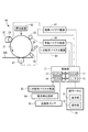
図1に示すように、画像形成装置1は、装置本体10と、不図示のシート給送部と、画像形成部40と、不図示のシート排出部と、制御部11と、温湿度センサ70と、操作パネル30とを備えている。画像形成装置1は、不図示の原稿読取装置、パーソナルコンピュータ等のホスト機器、あるいはデジタルカメラやスマートフォン等の外部機器からの画像信号に応じて、4色フルカラー画像を記録材に形成することができる。尚、記録材であるシートSは、トナー像が形成されるものであり、具体例として、普通紙、普通紙の代用品である合成樹脂製のシート、厚紙、オーバーヘッドプロジェクタ用シート等がある。
As shown in FIG. 1, the image forming apparatus 1 includes an apparatus
画像形成部40は、シート給送部から給送されたシートSに対して、画像情報に基づいて画像を形成可能である。画像形成部40は、画像形成ユニット50y,50m,50c,50kと、トナーボトル41y,41m,41c,41kと、露光装置42y,42m,42c,42kと、中間転写ユニット44と、二次転写部45と、定着部46とを備えている。尚、本実施の形態の画像形成装置1は、フルカラーに対応するものであり、画像形成ユニット50y,50m,50c,50kは、イエロー(y)、マゼンタ(m)、シアン(c)、ブラック(k)の4色それぞれに同様の構成で別個に設けられている。このため、図1中では4色の各構成について同符号の後に色の識別子を付して示すが、図2及び明細書中では色の識別子を付さずに符号のみで説明する場合もある。
The
画像形成ユニット50は、トナー画像を形成する感光ドラム(像担持体)51と、帯電ローラ52と、現像装置20と、前露光装置54と、規制ブレード55と、を有している。画像形成ユニット50は、プロセスカートリッジとして一体にユニット化されて、装置本体10に対して着脱可能に構成されている。
The
感光ドラム51は、回転可能であり、画像形成に用いられる静電像を担持する。感光ドラム51は、本実施の形態では、外径30mmの負帯電性の有機感光体(OPC)であり、例えば210mm/secのプロセススピード(周速度)で矢印方向に回転駆動される。感光ドラム51は、アルミニウム製シリンダを基体とし、その表面に表面層として、順に塗布して積層された下引き層と、光電荷発生層と、電荷輸送層との3層を有している。
The
帯電ローラ52は、感光ドラム51の表面に接触し、従動して回転するゴムローラを用いており、感光ドラム51の表面を均一に帯電する。図2に示すように、帯電ローラ52には、帯電バイアス電源60が接続されている。帯電バイアス電源60は、帯電ローラ52に帯電バイアスとして直流電圧を印加し、帯電ローラ52を介して感光ドラム51を帯電する。露光装置42は、レーザスキャナであり、制御部11から出力される分解色の画像情報に従って、レーザ光を発する。
The charging
現像装置20は、現像バイアスが印加されることにより感光ドラム51に形成された静電像を、収容されたトナーにより現像する。現像装置20は、現像スリーブ24を有している。現像スリーブ24には、現像バイアスを印加するための現像バイアス電源61が接続されている。
The developing apparatus 20 develops an electrostatic image formed on the
感光ドラム51に現像されたトナー像は、後述する中間転写ベルト44bに一次転写される。一次転写後の感光ドラム51は、前露光装置54によって表面を除電される。規制ブレード55は、カウンターブレード方式であり、ブレードの自由長を8mmとするウレタンを主体とした弾性ブレードで、感光ドラム51に対して所定の押圧力で当接されている。
The toner image developed on the
図1に示すように、中間転写ユニット44は、駆動ローラ44aや従動ローラ44d、一次転写ローラ47y,47m,47c,47k等の複数のローラと、これらのローラに巻き掛けられ、トナー像を担持する中間転写ベルト44bとを備えている。一次転写ローラ47y,47m,47c,47kは、感光ドラム51y,51m,51c,51kにそれぞれ対向して配置され、中間転写ベルト44bに当接する。
As shown in FIG. 1, the intermediate transfer unit 44 is wound around a plurality of rollers such as a driving roller 44a, a driven
一次転写ローラ47は、感光ドラム51に対向し、中間転写ベルト44bの内側に設けられている。一次転写ローラ47は、材質がSUM(硫黄及び硫黄複合快削鋼)或いはSUS(ステンレス鋼)などの金属ローラで形成されている。一次転写ローラ47はスラスト方向にストレートの形状であり、ローラ径は6〜10mm程度である。一次転写ローラ47には、一次転写バイアスを印加するための一次転写バイアス電源62(図2参照)が接続され、一次転写バイアス電源62からトナーの帯電極性と逆極性の電圧が印加される。これにより、感光ドラム51の表面電位と一次転写ローラ47の電位の電位差である一次転写コントラストが形成される。各一次転写部にそれぞれ所定の一次転写コントラストが形成されることで、各々の感光ドラム51のトナー像が、中間転写ベルト44bに順次、静電吸引され、中間転写ベルト44b上に重畳されたトナー像が形成される。
The
中間転写ベルト(中間転写体)44bは、感光ドラム51との間で一次転写部を形成し、一次転写バイアスが印加されることにより、感光ドラム51に形成されたトナー像を一次転写部で一次転写する。中間転写ベルト44bに一次転写ローラ47によって正極性の一次転写バイアスを印加することにより、感光ドラム51上のそれぞれの負極性を持つトナー像が順次中間転写ベルト44bに多重転写される。中間転写ベルト44bには、29〜118N(約3〜12kgf)程度の張力が付与されている。
The intermediate transfer belt (intermediate transfer body) 44b forms a primary transfer portion with the
中間転写ベルト44bは、単層で構成された無端状のベルトである。具体的な材料は以下の通りであり、例えば、ポリイミド、ポリカーボネート、ポリフッ化ビニリデン(PVDF)、ポリフェニレンサルファイド、ポリエチレン、ポリプロピレン、ポリスチレン、ポリアミド、ポリサルフォン、ポリアリレート。そして、ポリエチレンテレフタレート、ポリブチレンテレフタレート、ポリエーテルサルフォン、ポリエーテルニトリル、エチレンテトラフルオロエチレン共重合体、ポリエーテルエーテルケトンなどの単体樹脂、またはこれらの混合物が使用可能である。
The
本実施の形態では、中間転写ベルト44bの材料としてポリイミド樹脂、またはポリエーテルエーテルケトン樹脂を使用している。そして、中間転写ベルト44bの厚みは、60〜70μm程度としている。中間転写ベルト44bの表面抵抗率は、1.0×10¹²Ω/□以上2.0×1012Ω/□以下、体積抵抗率は4.0×1011Ω・cm以上6.0×1011Ω・cm以下としている。尚、抵抗の測定は、ハイレスタUP(三菱化学製)の測定器と、URS(ガード電極外径φ17.9mm)(三菱化学製)の測定プローブとを用いて、印加電圧100V、チャージ10秒の測定条件で行った。
In this embodiment, a polyimide resin or a polyetheretherketone resin is used as the material of the
二次転写部45は、二次転写内ローラ45aと、二次転写外ローラ(二次転写手段)45bとを備えている。二次転写内ローラ45aは、芯金の周囲にEPDM(エチレン・プロピレン・ジエンゴム)を設けることで構成される。二次転写内ローラ45aは、ローラ径が20mm、ゴム厚0.5mmとなるように形成され、硬度は例えば70°(アスカーC)に設定される。また、二次転写内ローラ45aは、接地されている。
The
二次転写外ローラ45bには、二次転写外ローラ45bに二次転写バイアスを印加する二次転写バイアス電源(バイアス印加手段)63が接続されている。二次転写外ローラ45bは、中間転写ベルト44bに当接して中間転写ベルト44bとの間で二次転写部45を形成し、二次転写バイアスが印加されることにより、中間転写ベルト44bに一次転写されたトナー像を二次転写部45でシートSに二次転写する。二次転写外ローラ45bは、芯金の周囲に金属錯体などのイオン導電剤を含有したNBR(ニトリルゴム)やEPDMなどからなる弾性層を設けることで構成される。二次転写外ローラ45bは、芯金径が12mm、弾性層を含むローラ径が24mmになるように形成されている。二次転写外ローラ45bの抵抗値は3.0×10⁷〜5.0×10⁷Ωとし、二次転写部45において、二次転写内ローラ45aと中間転写ベルト44bの抵抗値は二次転写外ローラ45bの抵抗値より十分小さくなっている。二次転写外ローラ45bには、二次転写外ローラ45bに流れる電流を検出可能な電流検出回路(電流検出手段)64(図2参照)が接続されている。
A secondary transfer bias power supply (bias applying means) 63 that applies a secondary transfer bias to the secondary transfer
定着部46は、定着ローラ46a及び加圧ローラ46bを備えている。定着ローラ46aと加圧ローラ46bとの間をシートSが挟持され搬送されることにより、シートSに転写されたトナー像は加熱及び加圧されてシートSに定着される。シート排出部は、定着後、排出経路から搬送されるシートSを給送し、例えば、排出口から排出して排出トレイに積載する。
The fixing
図2に示すように、制御部11はコンピュータにより構成され、例えばCPU12と、各部を制御するプログラムを記憶するROM13と、データを一時的に記憶するRAM14と、外部と信号を入出力する入出力回路(I/F)15とを備えている。CPU12は、画像形成装置1の制御全体を司るマイクロプロセッサであり、システムコントローラの主体である。CPU12は、入出力回路15を介して、シート給送部、画像形成部40、シート排出部、操作パネル30に接続され、各部と信号をやり取りすると共に動作を制御する。ROM13には、シートSに画像を形成するための画像形成制御シーケンス等が記憶される。操作パネル30は、表示部31と操作部32とを有しており(図3参照)、二次転写バイアスの設定を変更可能である。ユーザは、操作パネル30の操作部32を操作することにより、プリント枚数、シート段のシート種、サイズなどを設定することができる。操作部32は、出力電圧の目標値に関する値を入力可能である。
As shown in FIG. 2, the
制御部11には、帯電バイアス電源60と、現像バイアス電源61と、一次転写バイアス電源62と、二次転写バイアス電源63と、電流検出回路64と、温湿度センサ70とが接続されている。温湿度センサ70は、装置本体10の内部に設けられ、温度及び湿度を検知可能である。制御部11は、温湿度センサ70から温度及び湿度、又は絶対水分量を検知可能である。また、制御部11は、温湿度センサ70の検知結果により、ROM13に記憶したテーブルに基づいて二次転写バイアスを決定している。テーブルは、所望の二次転写電流が流れるように、温度及び湿度と二次転写バイアスとの関係を予め求めて設定したものとしている。
A charging
制御部11は、二次転写バイアス電源63が印加する二次転写バイアスが所定の上限電圧を超えて設定されないように二次転写バイアス電源63を制御する(図5のステップS17)。また、制御部11は、非画像形成時に二次転写外ローラ45bにテストバイアスを印加したときに電流検出回路64で検出された電流と、該印加したテストバイアスと、に基づいて、高圧上限Vlimを変更する(図5のステップS12)。制御部11は、操作部32から変更された二次転写バイアスが高圧上限Vlimを超えた場合に、二次転写バイアスを高圧上限Vlimに設定する(図5のステップS17)。制御部11は、非画像形成時に印加した異なる複数のテストバイアスとそれぞれ電流検出回路64で検出された電流との関係、及び二次転写バイアス電源63の所定の高圧保証範囲の電圧と電流との関係に基づいて、高圧上限Vlimを設定する。尚、二次転写バイアスは負である場合もあるので、ここでは二次転写バイアスの絶対値の高圧上限Vlimを設定している。
The
尚、本実施の形態では、画像形成時とは、画像形成装置1に備えられたスキャナやパーソナルコンピュータなどの外部端末から入力された画像情報に基づいて、感光ドラム51にトナー像を形成しているときである。一方、非画像形成時とは、画像形成時以外のときであり、例えば、画像形成ジョブが実行されていないときの他、画像形成ジョブ中の前回転時や紙間等である。また、画像形成ジョブとは、プリント命令信号(画像形成指令信号)に基づいて行う次のような一連の動作のことである。即ち、画像形成を行うにあたり必要となる予備動作(所謂、前回転動作)を開始してから、画像形成工程を経て、画像形成を終了するにあたり必要となる予備動作(所謂、後回転)が完了するまでの一連の動作のことである。具体的には、プリント命令信号を受けた(画像形成ジョブの入力)後の前回転時(画像形成前の準備動作)から、後回転(画像形成後の動作)までのことを指し、画像形成期間、紙間(非画像形成時)を含む。更に、紙間とは、連続して画像形成が行われる場合に、シート1枚に対して形成されるトナー像と次のシート1枚に対して形成されるトナー像との間に相当する期間である。
In the present embodiment, at the time of image formation, a toner image is formed on the
次に、このように構成された画像形成装置1における画像形成動作について、図1を用いて説明する。 Next, the image forming operation in the image forming apparatus 1 configured in this way will be described with reference to FIG.
画像形成動作が開始されると、まず感光ドラム51が回転して表面が帯電ローラ52により帯電される。そして、露光装置42により画像情報に基づいてレーザ光が感光ドラム51に対して発光され、感光ドラム51の表面上に静電潜像が形成される。この静電潜像にトナーが付着することにより、現像されてトナー画像として可視化され、中間転写ベルト44bに転写される。
When the image forming operation is started, the
一方、このようなトナー像の形成動作に並行してシートSが供給され、中間転写ベルト44bのトナー画像にタイミングを合わせて、搬送経路を介してシートSが二次転写部45に搬送される。更に、中間転写ベルト44bからシートSに画像が転写され、シートSは、定着部46に搬送され、ここで未定着トナー像が加熱及び加圧されてシートSの表面に定着され、装置本体10から排出される。
On the other hand, the sheet S is supplied in parallel with the toner image forming operation, and the sheet S is conveyed to the
ここで、二次転写バイアス電源63の所定の高圧保証範囲について説明する。二次転写バイアス電源63から出力される二次転写バイアスは、可変となっている。二次転写バイアス電源63は、高圧保証範囲を有した定電圧制御にて高圧出力を行うものであり、この高圧保証範囲外となるような電流が設定された場合には、発熱や高圧回路内の放電による破壊を回避するための間欠出力動作するよう設定されている。高圧保証範囲を示す電圧−電流の情報は、予め制御部11のROM13に記憶されている。
Here, a predetermined high voltage guarantee range of the secondary transfer bias
図4(a)に示すように、高圧保証範囲の境界(図中、破線で示す)を示す数式は、以下の2式で示される。
I=a×V+b(0≦V<Cのとき) (数式1)
V=C(V≧Cのとき) (数式2)
As shown in FIG. 4A, the mathematical formula indicating the boundary of the high voltage guarantee range (indicated by the broken line in the figure) is shown by the following two equations.
I = a × V + b (when 0 ≦ V <C) (Formula 1)
V = C (when V ≧ C) (Formula 2)
尚、本実施の形態では、上記の2つの数式で示された高圧保証範囲の高圧基板について説明するが、高圧保証範囲は高圧回路設計によって異なるものであり、上記の数式で定義されたものに限定されるものではない。 In the present embodiment, the high-voltage substrate in the high-voltage guarantee range shown by the above two mathematical formulas will be described, but the high-voltage guarantee range differs depending on the high-voltage circuit design, and is defined by the above mathematical formula. It is not limited.
画像形成時に二次転写部45に印加される電圧V2trは、下記の数式3により算出される。制御部11は、非通紙時に決定される電圧Vbと、紙分担電圧テーブルより与えられるVpとを足し合わせて、その電圧V2trをシートの二次転写部45の通過時に二次転写外ローラ45bに印加し、中間転写ベルト44bのトナー像をシートに転写する。
V2tr=Vb+Vp (数式3)
The voltage V2tr applied to the
V2tr = Vb + Vp (Formula 3)
二次転写外ローラ45bは、上述のようにイオン導電剤を分散したスポンジゴム材料であるため、耐久状態によって劣化し抵抗値が変動する。また、温度や湿度によっても電気抵抗は変動するため、作像時のローラ抵抗に合わせた電圧設定が必要である。本実施の形態では、プリント動作中の非通紙時に、2種以上のテストバイアスを二次転写外ローラ45bに印加し、二次転写部45に流れる電流を電流検出回路64にて検出する。図4(a)に示すように、2点のテストバイアスの印加電圧とそれぞれ検出された電流値とに基づき、傾きα及び切片βを算出し、I=V×α+βの関係(V−I直線)を得る。そして、所望の転写電流を得るための電圧値を決定する自動転写電圧制御(以下、ATVCという)を実行する。即ち、制御部11が作像動作時にATVCを実行することで、その時々のローラ抵抗に合わせた電圧設定が可能となり、図4(a)に示すように、所望の電流(ターゲット電流It)を得るための電圧Vbを決定する。また、制御部11は、温湿度センサ70で検知した環境情報に対応する電圧値を紙分担テーブルより紙分担電圧Vpを決定する。以上により設定されたVb及びVpを利用して、画像形成時に二次転写部45に印加される電圧V2trを算出することができる。
Since the secondary transfer
上述したVbあるいはVpを変更する場合について、以下に説明する。図3に示すように、操作パネル30の表示部31には、シート種毎に1面目及び2面目の二次転写設定を調整可能な項目が表示され、基準値(“0”表示時)に対して、操作部32から調整値を入力することで紙分担電圧Vpを増減させることができる。例えば、ユーザが体積抵抗率の高い(低い)シートをプリントする場合は、予め与えられた紙分担電圧テーブル値を基準に紙抵抗差分に相当するオフセット電圧Vposを増加(あるいは減少)するよう二次転写設定を変更することが可能である。制御部11は、ユーザが入力した紙分担電圧設定にて決められたオフセット電圧Vposに基づいて、Vp’=Vp+Vposとして、VpではなくVp’を二次転写電圧決定時に反映させる。
The case of changing Vb or Vp described above will be described below. As shown in FIG. 3, the
ここで、二次転写高圧上限(上限電圧)Vlimについて説明する。制御部11がATVC実行時に求めたV−I直線と、高圧保証領域を示す数式1(I=a×V+b)との交点より与えられる電圧を、下記の数式4により算出し、二次転写高圧上限Vlimに設定する。
Vlim=(β−b)/(a−α) (数式4)
Here, the secondary transfer high voltage upper limit (upper limit voltage) Vlim will be described. The voltage given from the intersection of the VI straight line obtained by the
Vlim = (β-b) / (a-α) (Formula 4)
即ち、二次転写部45のATVCと操作部32で決定した二次転写設定で、Vlimを超える電圧値が設定された場合、V2trをVlimに設定し、高圧保証範囲外の電流値を出力させないようにする。例えば、高温高湿環境下においては二次転写外ローラ45bのローラ抵抗値が低下するため、ユーザが誤って操作部32で入力可能な紙分担電圧Vpのオフセット電圧を大きく設定してしまった場合、高圧保証範囲外の過電流を設定してしまうことがある。このような場合に過電流保護回路が動作し、二次転写バイアス電源63が間欠出力を行うため、中間転写ベルト44bのトナー像がシートへ最適には転写されず高圧電下の間欠出力を反映した縞状の画像が出力されてしまい、画像情報が欠落してしまう。そこで、本実施の形態の画像形成装置1により、意図せず高圧保証範囲外の電圧値を設定されるような場合でも、保護回路動作が実行される電圧設定にならないように二次転写バイアスを決定するため、このような画像情報が欠落するような事態は回避される。尚、Vlimは高圧出力精度、電流検知精度、電圧検知精度、ローラ抵抗の振れ等のバラつきを考慮し、Vlimよりも少し低め(例えば、Vlim’=Vlim×95%)に設定しておくことが望ましい。
That is, when a voltage value exceeding Vlim is set in the secondary transfer setting determined by the ATVC of the
次に、本実施の形態の画像形成装置1における紙間ATVCについて説明する。二次転写外ローラ45bのローラ抵抗等を含めた二次転写部45のインピーダンスは、画像形成装置1の使用モードや環境によって変化する。ユーザの使用環境自体が変化する場合、二次転写部45のインピーンダンス変化の要因は様々である。例えば、連続プリント枚数が多く定着部46からの放射熱により装置本体10内が昇温する場合がある。あるいは、両面プリントモードにおいては1面目で定着後にシートが温められた直後に2面目が二次転写部45を通過することから、二次転写外ローラ45bが温められる場合等がある。
Next, the inter-paper ATVC in the image forming apparatus 1 of the present embodiment will be described. The impedance of the
このようなインピーダンスの変化に応じて、連続プリントモード中の紙間制御で2点以上のテストバイアス印加により二次転写のインピーダンスを再設定する制御(紙間ATVC)を行う場合には、制御部11は高圧上限Vlimの再計算を行う。制御部11は、紙間ATVCで二転インピーダンスの変化を検知し、二転設定の補正が必要と判断した場合に二次転写設定の変更を行うと共に、高圧上限Vlimも変化させる。
When performing control (paper-to-paper ATVC) to reset the impedance of the secondary transfer by applying a test bias of two or more points in the paper-to-paper control in the continuous print mode in response to such a change in impedance, the
本実施の形態では、制御部11は、紙間ATVCとして、連続通紙中の非通紙タイミング中に2種類以上のテストバイアスを印加し、その時の電流を検知する。そして、制御部11は、検知電流と印加電圧との関係から、Vb印加時の電流Iinを算出し、所望の電流Itからの乖離を判断し二次転写バイアスを補正する。そして、制御部11は、検知された電流とターゲット電流Itとの乖離量が所定量ΔIth以上の場合は、所望の範囲に電流値が近づけるように印加電圧をオフセットさせる。具体的には、以下の判断式となる。
Iin>It かつ Iin−It>ΔIthの場合は、Vb’=Vb−ΔV
Iin>It かつ Iin−It≦ΔIthの場合は、Vb’=Vb
Iin<It かつ It−Iin>ΔIthの場合は、Vb’=Vb+ΔV
Iin<It かつ It−Iin≦ΔIthの場合は、Vb’=Vb
In the present embodiment, the
When Iin> It and Iin-It> ΔIt, Vb'= Vb-ΔV
If Iin> It and Iin-It ≤ ΔIth, Vb'= Vb
In the case of Iin <It and It-Iin> ΔIth, Vb'= Vb + ΔV
If Iin <It and It-Iin ≤ ΔIth, Vb'= Vb
そして、制御部11は、紙間ATVCにおいて、2種のテストバイアスと、それぞれのバイアス印加時に電流検出回路64にて検出した電流とでV−I直線を計算し、高圧保証領域を示す数式1との交点より新たにVlimを算出して更新する。
Then, the
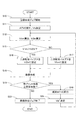
次に、本実施の形態の画像形成装置1において、画像形成時に二次転写バイアスを設定する手順について、図5に沿って説明する。尚、ユーザは、操作部32を用いて予め1面目及び2面目の二次転写設定を調整して入力しているものとする。
Next, in the image forming apparatus 1 of the present embodiment, a procedure for setting a secondary transfer bias at the time of image forming will be described with reference to FIG. It is assumed that the user uses the
画像形成ジョブが開始されると(ステップS10)、前回転時に制御部11はATVCを実行し、Vbを決定する(ステップS11)。そして、制御部11は、数式4に基づいて高圧上限Vlimを算出すると共に、数式3に基づいて画像形成時に二次転写部45に印加される電圧V2trを算出する(ステップS12)。更に、制御部11は、高圧上限Vlimが電圧V2trを超えているか否かを判断する(ステップS15)。制御部11が、高圧上限Vlimは電圧V2trを超えていると判断した場合は、二次転写バイアスを電圧V2trに設定する(ステップS16)。一方、制御部11は、高圧上限Vlimは電圧V2trを超えていないと判断した場合は、二次転写バイアスを高圧上限Vlimに設定する(ステップS17)。そして、制御部11は、設定した二次転写バイアスにより画像形成を実行する(ステップS18)。
When the image forming job is started (step S10), the
制御部11は、本画像形成ジョブにおいて、残プリント枚数が予め設定された所定のプリント枚数以上であるか判断する(ステップS19)。制御部11は、残プリント枚数が予め設定された所定のプリント枚数以上であると判断した場合は、所定のタイミングにおいて紙間ATVCを実行して(ステップS20)、Vbを更新して、新たにVb’を算出する(ステップS21)。そして、制御部11は、次の画像形成処理に向けて、高圧上限Vlimを算出する(ステップS12)。ステップS19において、制御部11は、残プリント枚数が予め設定された所定のプリント枚数以上でないと判断した場合は、画像形成ジョブを終了する(ステップS22)。
In this image forming job, the
上述したように本実施の形態の画像形成装置1によれば、制御部11は、非画像形成時に二次転写外ローラ45bにテストバイアスを印加した時に電流検出回路64で検出された電流と、印加したテストバイアスと、に基づいて、高圧上限Vlimを変更する。このため、テストバイアスと検出電流とに基づいて、二次転写バイアス電源63が印加可能な高圧上限Vlimを適正な大きさに変更することができる。これにより、転写電圧をユーザ設定可能でありながら画像不良の発生を抑制でき、しかも転写電圧の設定範囲を不要に狭くすることを防止できる。
As described above, according to the image forming apparatus 1 of the present embodiment, the
尚、上述した実施の形態の画像形成装置1では、画像形成装置1は、中間転写ベルト44bを有し、感光ドラム51から中間転写ベルト44bに各色のトナー像を一次転写した後、各色の複合トナー像をシートSに一括して二次転写する方式としている。但し、これには限られず、シート搬送ベルトで搬送されたシートに感光ドラムから直接に転写する方式を採用してもよい。この場合、画像形成装置は、感光ドラムとの間で転写部を形成し、転写バイアスが印加されることにより、感光ドラムに形成されたトナー像を転写部でシートに転写する転写手段を備える。そして、制御部11は、非画像形成時に転写手段にテストバイアスを印加したときに電流検出手段で検出された電流と、該印加したテストバイアスと、に基づいて、高圧上限Vlimを変更する。この場合も、バイアス印加手段が印加可能な高圧上限Vlimを適正な大きさに変更することができるので、転写電圧をユーザ設定可能でありながら画像不良の発生を抑制でき、しかも転写電圧の設定範囲を不要に狭くすることを防止できる。
In the image forming apparatus 1 of the above-described embodiment, the image forming apparatus 1 has an
1…画像形成装置、11…制御部、32…操作部、44b…中間転写ベルト(中間転写体)、45…二次転写部、45b…二次転写外ローラ(二次転写手段)、51,51c,51k,51m,51y…感光ドラム(像担持体)、63…二次転写バイアス電源(バイアス印加手段)、64…電流検出回路(電流検出手段)、S…シート(記録材)、Vlim…高圧上限(上限電圧)。 1 ... Image forming apparatus, 11 ... Control unit, 32 ... Operation unit, 44b ... Intermediate transfer belt (intermediate transfer body), 45 ... Secondary transfer unit, 45b ... Secondary transfer outer roller (secondary transfer means), 51, 51c, 51k, 51m, 51y ... Photosensitive drum (image carrier), 63 ... Secondary transfer bias power supply (bias application means), 64 ... Current detection circuit (current detection means), S ... Sheet (recording material), Voltage ... High voltage upper limit (upper limit voltage).
Claims (4)
前記像担持体に形成されたトナー像が転写される中間転写体と、
転写バイアスが印加され、前記中間転写体から記録材にトナー像を転写する転写手段と、
前記転写手段に前記転写バイアスを印加するバイアス印加手段と、
前記転写手段に流れる電流を検出可能な電流検出手段と、
前記転写手段に流れる電流及び印加される電圧の関係が所定範囲を超える電流が出力された場合に、前記転写手段に印加する転写バイアスを強制的に停止する停止動作を行う保護回路と、
前記転写バイアスの設定値を手動入力により調整可能な操作部と、
非画像形成時に前記転写手段に印加した異なる複数のテストバイアスと、該複数のテストバイアスを印加した際に前記電流検出手段で検出した複数の電流と、前記保護回路が作動する電流と電圧の関係に関する情報と、に基づいて、前記保護回路が作動する電流値を出力させない電圧値の上限値としての上限電圧値を取得し、前記操作部で調整された前記転写バイアスの設定値が前記上限電圧値を超えている場合は、前記転写バイアスの設定値が前記上限電圧値を超えないように前記バイアス印加手段を制御する制御部と、を備える、
ことを特徴とする画像形成装置。 An image forming means for forming a toner image on an image carrier,
An intermediate transfer body to which the toner image formed on the image carrier is transferred, and
A transfer means for transferring a toner image from the intermediate transfer body to a recording material by applying a transfer bias,
A bias applying means for applying the transfer bias to the transfer means, and
A current detecting means capable of detecting the current flowing through the transfer means, and
A protection circuit that performs a stop operation for forcibly stopping the transfer bias applied to the transfer means when a current whose relationship between the current flowing through the transfer means and the applied voltage exceeds a predetermined range is output .
An operation unit that can adjust the transfer bias setting value by manual input ,
Relationship between a plurality of different test biases applied to the transfer means during non-image formation, a plurality of currents detected by the current detecting means when the plurality of test biases are applied, and a current and a voltage at which the protection circuit operates. Based on the information regarding the above, the upper limit voltage value as the upper limit value of the voltage value that does not output the current value in which the protection circuit operates is acquired, and the set value of the transfer bias adjusted by the operation unit is the upper limit voltage. When the value is exceeded, a control unit for controlling the bias applying means so that the set value of the transfer bias does not exceed the upper limit voltage value is provided.
An image forming apparatus characterized in that.
前記基準電圧と、トナー像が転写される記録材の種類に対応して定められた所定の分担電圧と、に基づいて、前記転写バイアスを設定する、
ことを特徴とする請求項1に記載の画像形成装置。 The control unit applies the plurality of different test biases applied to the transfer means and the plurality of currents detected by the current detecting means when the plurality of test biases are applied to the transfer means. Set the reference voltage for passing a predetermined current,
The transfer bias is set based on the reference voltage and a predetermined shared voltage determined according to the type of recording material on which the toner image is transferred.
The image forming apparatus according to claim 1.
前記操作部で調整された前記転写バイアスが前記上限電圧値を超える場合は、前記上限電圧を前記転写バイアスとして設定する、
ことを特徴とする請求項1又は2に記載の画像形成装置。 When the transfer bias adjusted by the operation unit does not exceed the upper limit voltage value , the control unit sets the set value of the transfer bias adjusted by the operation unit as the transfer bias.
When the transfer bias adjusted by the operation unit exceeds the upper limit voltage value , the upper limit voltage is set as the transfer bias.
The image forming apparatus according to claim 1 or 2.
ことを特徴とする請求項1乃至3のいずれか1項に記載の画像形成装置。 The image forming apparatus according to any one of claims 1 to 3, wherein the image forming apparatus is characterized.
Priority Applications (2)
| Application Number | Priority Date | Filing Date | Title |
|---|---|---|---|
| JP2016138695A JP6765882B2 (en) | 2016-07-13 | 2016-07-13 | Image forming device |
| US15/642,714 US10234797B2 (en) | 2016-07-13 | 2017-07-06 | Image forming apparatus |
Applications Claiming Priority (1)
| Application Number | Priority Date | Filing Date | Title |
|---|---|---|---|
| JP2016138695A JP6765882B2 (en) | 2016-07-13 | 2016-07-13 | Image forming device |
Publications (3)
| Publication Number | Publication Date |
|---|---|
| JP2018010140A JP2018010140A (en) | 2018-01-18 |
| JP2018010140A5 JP2018010140A5 (en) | 2019-08-22 |
| JP6765882B2 true JP6765882B2 (en) | 2020-10-07 |
Family
ID=60995388
Family Applications (1)
| Application Number | Title | Priority Date | Filing Date |
|---|---|---|---|
| JP2016138695A Active JP6765882B2 (en) | 2016-07-13 | 2016-07-13 | Image forming device |
Country Status (1)
| Country | Link |
|---|---|
| JP (1) | JP6765882B2 (en) |
Families Citing this family (3)
| Publication number | Priority date | Publication date | Assignee | Title |
|---|---|---|---|---|
| JP7250469B2 (en) * | 2018-05-25 | 2023-04-03 | キヤノン株式会社 | image forming device |
| EP3805866B1 (en) | 2018-05-25 | 2024-01-24 | Canon Kabushiki Kaisha | Image formation device |
| US11143989B2 (en) * | 2018-08-09 | 2021-10-12 | Canon Kabushiki Kaisha | Image forming apparatus |
Family Cites Families (3)
| Publication number | Priority date | Publication date | Assignee | Title |
|---|---|---|---|---|
| JP2004101967A (en) * | 2002-09-10 | 2004-04-02 | Canon Inc | Image forming apparatus |
| JP4935805B2 (en) * | 2008-12-22 | 2012-05-23 | コニカミノルタビジネステクノロジーズ株式会社 | Image forming apparatus |
| US20150378283A1 (en) * | 2014-06-27 | 2015-12-31 | Kabushiki Kaisha Toshiba | Image forming apparatus |
-
2016
- 2016-07-13 JP JP2016138695A patent/JP6765882B2/en active Active
Also Published As
| Publication number | Publication date |
|---|---|
| JP2018010140A (en) | 2018-01-18 |
Similar Documents
| Publication | Publication Date | Title |
|---|---|---|
| US10234797B2 (en) | Image forming apparatus | |
| CN111665702B (en) | Image forming apparatus having a plurality of image forming units | |
| US9891561B2 (en) | Image forming device and method of acquiring photoreceptor layer thickness | |
| US20180253039A1 (en) | Image forming apparatus | |
| US20080124103A1 (en) | Image forming apparatus capable of controlling application voltage to adhering member | |
| CN114026503B (en) | Image forming apparatus having a plurality of image forming units | |
| JP2020086107A (en) | Image forming device | |
| JP6765882B2 (en) | Image forming device | |
| JP6765883B2 (en) | Image forming device | |
| JP7383458B2 (en) | image forming device | |
| JP6789804B2 (en) | Image forming device | |
| EP3070532A1 (en) | Image forming apparatus and image forming method | |
| JP2020027144A (en) | Image forming apparatus | |
| JP2019086596A (en) | Image forming apparatus | |
| JP7350536B2 (en) | Image forming device | |
| JP7353856B2 (en) | Image forming device | |
| JP5904844B2 (en) | Image forming apparatus | |
| US11768452B2 (en) | Image forming apparatus | |
| KR102621420B1 (en) | image forming device | |
| JP7350537B2 (en) | Image forming device | |
| JP6489074B2 (en) | Image forming apparatus | |
| JP2024027750A (en) | image forming device | |
| JP2017097033A (en) | Image formation device | |
| KR20220114473A (en) | Image forming apparatus | |
| JP2022063810A (en) | Image forming apparatus |
Legal Events
| Date | Code | Title | Description |
|---|---|---|---|
| A521 | Written amendment |
Free format text: JAPANESE INTERMEDIATE CODE: A523 Effective date: 20190710 |
|
| A621 | Written request for application examination |
Free format text: JAPANESE INTERMEDIATE CODE: A621 Effective date: 20190710 |
|
| RD02 | Notification of acceptance of power of attorney |
Free format text: JAPANESE INTERMEDIATE CODE: A7422 Effective date: 20200206 |
|
| RD04 | Notification of resignation of power of attorney |
Free format text: JAPANESE INTERMEDIATE CODE: A7424 Effective date: 20200207 |
|
| A977 | Report on retrieval |
Free format text: JAPANESE INTERMEDIATE CODE: A971007 Effective date: 20200527 |
|
| A131 | Notification of reasons for refusal |
Free format text: JAPANESE INTERMEDIATE CODE: A131 Effective date: 20200609 |
|
| A521 | Written amendment |
Free format text: JAPANESE INTERMEDIATE CODE: A523 Effective date: 20200731 |
|
| TRDD | Decision of grant or rejection written | ||
| A01 | Written decision to grant a patent or to grant a registration (utility model) |
Free format text: JAPANESE INTERMEDIATE CODE: A01 Effective date: 20200818 |
|
| A61 | First payment of annual fees (during grant procedure) |
Free format text: JAPANESE INTERMEDIATE CODE: A61 Effective date: 20200916 |
|
| R151 | Written notification of patent or utility model registration |
Ref document number: 6765882 Country of ref document: JP Free format text: JAPANESE INTERMEDIATE CODE: R151 |