JP6730948B2 - Optical device and manufacturing method thereof - Google Patents
Optical device and manufacturing method thereof Download PDFInfo
- Publication number
- JP6730948B2 JP6730948B2 JP2017029924A JP2017029924A JP6730948B2 JP 6730948 B2 JP6730948 B2 JP 6730948B2 JP 2017029924 A JP2017029924 A JP 2017029924A JP 2017029924 A JP2017029924 A JP 2017029924A JP 6730948 B2 JP6730948 B2 JP 6730948B2
- Authority
- JP
- Japan
- Prior art keywords
- convex portion
- resin member
- optical device
- jig
- layer
- Prior art date
- Legal status (The legal status is an assumption and is not a legal conclusion. Google has not performed a legal analysis and makes no representation as to the accuracy of the status listed.)
- Active
Links
- 230000003287 optical effect Effects 0.000 title claims description 60
- 238000004519 manufacturing process Methods 0.000 title claims description 17
- 239000011347 resin Substances 0.000 claims description 70
- 229920005989 resin Polymers 0.000 claims description 70
- 239000010410 layer Substances 0.000 claims description 38
- 239000000758 substrate Substances 0.000 claims description 33
- 239000004065 semiconductor Substances 0.000 claims description 26
- 239000000463 material Substances 0.000 claims description 19
- 239000002346 layers by function Substances 0.000 claims description 16
- 238000000034 method Methods 0.000 claims description 16
- 239000000853 adhesive Substances 0.000 claims description 14
- 230000001070 adhesive effect Effects 0.000 claims description 14
- 239000012790 adhesive layer Substances 0.000 claims description 7
- 239000002184 metal Substances 0.000 claims description 5
- 229910052751 metal Inorganic materials 0.000 claims description 5
- 239000012530 fluid Substances 0.000 claims description 4
- XUIMIQQOPSSXEZ-UHFFFAOYSA-N Silicon Chemical compound [Si] XUIMIQQOPSSXEZ-UHFFFAOYSA-N 0.000 description 35
- 239000011521 glass Substances 0.000 description 34
- 229910052710 silicon Inorganic materials 0.000 description 32
- 239000010703 silicon Substances 0.000 description 32
- 238000001514 detection method Methods 0.000 description 14
- 230000000903 blocking effect Effects 0.000 description 4
- RYGMFSIKBFXOCR-UHFFFAOYSA-N Copper Chemical compound [Cu] RYGMFSIKBFXOCR-UHFFFAOYSA-N 0.000 description 3
- 229910052802 copper Inorganic materials 0.000 description 3
- 239000010949 copper Substances 0.000 description 3
- 230000000694 effects Effects 0.000 description 3
- 238000007747 plating Methods 0.000 description 2
- 230000015572 biosynthetic process Effects 0.000 description 1
- 238000005516 engineering process Methods 0.000 description 1
- 238000010438 heat treatment Methods 0.000 description 1
- 239000011159 matrix material Substances 0.000 description 1
- 238000012986 modification Methods 0.000 description 1
- 230000004048 modification Effects 0.000 description 1
- 229910021421 monocrystalline silicon Inorganic materials 0.000 description 1
- 230000008646 thermal stress Effects 0.000 description 1
Images


Classifications
-
- H—ELECTRICITY
- H01—ELECTRIC ELEMENTS
- H01L—SEMICONDUCTOR DEVICES NOT COVERED BY CLASS H10
- H01L27/00—Devices consisting of a plurality of semiconductor or other solid-state components formed in or on a common substrate
- H01L27/14—Devices consisting of a plurality of semiconductor or other solid-state components formed in or on a common substrate including semiconductor components sensitive to infrared radiation, light, electromagnetic radiation of shorter wavelength or corpuscular radiation and specially adapted either for the conversion of the energy of such radiation into electrical energy or for the control of electrical energy by such radiation
- H01L27/144—Devices controlled by radiation
- H01L27/146—Imager structures
- H01L27/14601—Structural or functional details thereof
- H01L27/14618—Containers
-
- H—ELECTRICITY
- H01—ELECTRIC ELEMENTS
- H01L—SEMICONDUCTOR DEVICES NOT COVERED BY CLASS H10
- H01L27/00—Devices consisting of a plurality of semiconductor or other solid-state components formed in or on a common substrate
- H01L27/14—Devices consisting of a plurality of semiconductor or other solid-state components formed in or on a common substrate including semiconductor components sensitive to infrared radiation, light, electromagnetic radiation of shorter wavelength or corpuscular radiation and specially adapted either for the conversion of the energy of such radiation into electrical energy or for the control of electrical energy by such radiation
- H01L27/144—Devices controlled by radiation
- H01L27/146—Imager structures
- H01L27/14643—Photodiode arrays; MOS imagers
- H01L27/14649—Infrared imagers
-
- G—PHYSICS
- G01—MEASURING; TESTING
- G01J—MEASUREMENT OF INTENSITY, VELOCITY, SPECTRAL CONTENT, POLARISATION, PHASE OR PULSE CHARACTERISTICS OF INFRARED, VISIBLE OR ULTRAVIOLET LIGHT; COLORIMETRY; RADIATION PYROMETRY
- G01J1/00—Photometry, e.g. photographic exposure meter
- G01J1/02—Details
- G01J1/04—Optical or mechanical part supplementary adjustable parts
-
- G—PHYSICS
- G01—MEASURING; TESTING
- G01J—MEASUREMENT OF INTENSITY, VELOCITY, SPECTRAL CONTENT, POLARISATION, PHASE OR PULSE CHARACTERISTICS OF INFRARED, VISIBLE OR ULTRAVIOLET LIGHT; COLORIMETRY; RADIATION PYROMETRY
- G01J5/00—Radiation pyrometry, e.g. infrared or optical thermometry
- G01J5/02—Constructional details
- G01J5/0225—Shape of the cavity itself or of elements contained in or suspended over the cavity
- G01J5/024—Special manufacturing steps or sacrificial layers or layer structures
-
- H—ELECTRICITY
- H01—ELECTRIC ELEMENTS
- H01L—SEMICONDUCTOR DEVICES NOT COVERED BY CLASS H10
- H01L23/00—Details of semiconductor or other solid state devices
- H01L23/28—Encapsulations, e.g. encapsulating layers, coatings, e.g. for protection
- H01L23/29—Encapsulations, e.g. encapsulating layers, coatings, e.g. for protection characterised by the material, e.g. carbon
-
- H—ELECTRICITY
- H01—ELECTRIC ELEMENTS
- H01L—SEMICONDUCTOR DEVICES NOT COVERED BY CLASS H10
- H01L23/00—Details of semiconductor or other solid state devices
- H01L23/28—Encapsulations, e.g. encapsulating layers, coatings, e.g. for protection
- H01L23/31—Encapsulations, e.g. encapsulating layers, coatings, e.g. for protection characterised by the arrangement or shape
-
- H—ELECTRICITY
- H01—ELECTRIC ELEMENTS
- H01L—SEMICONDUCTOR DEVICES NOT COVERED BY CLASS H10
- H01L27/00—Devices consisting of a plurality of semiconductor or other solid-state components formed in or on a common substrate
- H01L27/14—Devices consisting of a plurality of semiconductor or other solid-state components formed in or on a common substrate including semiconductor components sensitive to infrared radiation, light, electromagnetic radiation of shorter wavelength or corpuscular radiation and specially adapted either for the conversion of the energy of such radiation into electrical energy or for the control of electrical energy by such radiation
- H01L27/144—Devices controlled by radiation
- H01L27/146—Imager structures
- H01L27/14601—Structural or functional details thereof
- H01L27/1462—Coatings
-
- H—ELECTRICITY
- H01—ELECTRIC ELEMENTS
- H01L—SEMICONDUCTOR DEVICES NOT COVERED BY CLASS H10
- H01L31/00—Semiconductor devices sensitive to infrared radiation, light, electromagnetic radiation of shorter wavelength or corpuscular radiation and specially adapted either for the conversion of the energy of such radiation into electrical energy or for the control of electrical energy by such radiation; Processes or apparatus specially adapted for the manufacture or treatment thereof or of parts thereof; Details thereof
- H01L31/02—Details
- H01L31/0203—Containers; Encapsulations, e.g. encapsulation of photodiodes
-
- H—ELECTRICITY
- H01—ELECTRIC ELEMENTS
- H01L—SEMICONDUCTOR DEVICES NOT COVERED BY CLASS H10
- H01L31/00—Semiconductor devices sensitive to infrared radiation, light, electromagnetic radiation of shorter wavelength or corpuscular radiation and specially adapted either for the conversion of the energy of such radiation into electrical energy or for the control of electrical energy by such radiation; Processes or apparatus specially adapted for the manufacture or treatment thereof or of parts thereof; Details thereof
- H01L31/02—Details
- H01L31/0232—Optical elements or arrangements associated with the device
- H01L31/02325—Optical elements or arrangements associated with the device the optical elements not being integrated nor being directly associated with the device
-
- H—ELECTRICITY
- H01—ELECTRIC ELEMENTS
- H01L—SEMICONDUCTOR DEVICES NOT COVERED BY CLASS H10
- H01L2224/00—Indexing scheme for arrangements for connecting or disconnecting semiconductor or solid-state bodies and methods related thereto as covered by H01L24/00
- H01L2224/01—Means for bonding being attached to, or being formed on, the surface to be connected, e.g. chip-to-package, die-attach, "first-level" interconnects; Manufacturing methods related thereto
- H01L2224/42—Wire connectors; Manufacturing methods related thereto
- H01L2224/47—Structure, shape, material or disposition of the wire connectors after the connecting process
- H01L2224/48—Structure, shape, material or disposition of the wire connectors after the connecting process of an individual wire connector
- H01L2224/4805—Shape
- H01L2224/4809—Loop shape
- H01L2224/48091—Arched
-
- H—ELECTRICITY
- H01—ELECTRIC ELEMENTS
- H01L—SEMICONDUCTOR DEVICES NOT COVERED BY CLASS H10
- H01L2224/00—Indexing scheme for arrangements for connecting or disconnecting semiconductor or solid-state bodies and methods related thereto as covered by H01L24/00
- H01L2224/01—Means for bonding being attached to, or being formed on, the surface to be connected, e.g. chip-to-package, die-attach, "first-level" interconnects; Manufacturing methods related thereto
- H01L2224/42—Wire connectors; Manufacturing methods related thereto
- H01L2224/47—Structure, shape, material or disposition of the wire connectors after the connecting process
- H01L2224/48—Structure, shape, material or disposition of the wire connectors after the connecting process of an individual wire connector
- H01L2224/481—Disposition
- H01L2224/48151—Connecting between a semiconductor or solid-state body and an item not being a semiconductor or solid-state body, e.g. chip-to-substrate, chip-to-passive
- H01L2224/48221—Connecting between a semiconductor or solid-state body and an item not being a semiconductor or solid-state body, e.g. chip-to-substrate, chip-to-passive the body and the item being stacked
- H01L2224/48245—Connecting between a semiconductor or solid-state body and an item not being a semiconductor or solid-state body, e.g. chip-to-substrate, chip-to-passive the body and the item being stacked the item being metallic
- H01L2224/48247—Connecting between a semiconductor or solid-state body and an item not being a semiconductor or solid-state body, e.g. chip-to-substrate, chip-to-passive the body and the item being stacked the item being metallic connecting the wire to a bond pad of the item
-
- H—ELECTRICITY
- H01—ELECTRIC ELEMENTS
- H01L—SEMICONDUCTOR DEVICES NOT COVERED BY CLASS H10
- H01L23/00—Details of semiconductor or other solid state devices
- H01L23/28—Encapsulations, e.g. encapsulating layers, coatings, e.g. for protection
- H01L23/31—Encapsulations, e.g. encapsulating layers, coatings, e.g. for protection characterised by the arrangement or shape
- H01L23/3107—Encapsulations, e.g. encapsulating layers, coatings, e.g. for protection characterised by the arrangement or shape the device being completely enclosed
-
- H—ELECTRICITY
- H01—ELECTRIC ELEMENTS
- H01L—SEMICONDUCTOR DEVICES NOT COVERED BY CLASS H10
- H01L27/00—Devices consisting of a plurality of semiconductor or other solid-state components formed in or on a common substrate
- H01L27/14—Devices consisting of a plurality of semiconductor or other solid-state components formed in or on a common substrate including semiconductor components sensitive to infrared radiation, light, electromagnetic radiation of shorter wavelength or corpuscular radiation and specially adapted either for the conversion of the energy of such radiation into electrical energy or for the control of electrical energy by such radiation
- H01L27/144—Devices controlled by radiation
- H01L27/146—Imager structures
- H01L27/14601—Structural or functional details thereof
- H01L27/14625—Optical elements or arrangements associated with the device
-
- H—ELECTRICITY
- H01—ELECTRIC ELEMENTS
- H01L—SEMICONDUCTOR DEVICES NOT COVERED BY CLASS H10
- H01L2924/00—Indexing scheme for arrangements or methods for connecting or disconnecting semiconductor or solid-state bodies as covered by H01L24/00
- H01L2924/15—Details of package parts other than the semiconductor or other solid state devices to be connected
- H01L2924/181—Encapsulation
- H01L2924/1815—Shape
Description
実施形態は、光学装置及びその製造方法に関する。 Embodiments relate to an optical device and a method for manufacturing the same.
近年、自動車の自動運転を実現するための技術の一つとして、車載用の赤外線センサが開発されている。赤外線センサは、受光部が形成された半導体チップを基板に搭載し、受光部上にガラス板を配置することにより、作製される。自動運転を実現するためには、自動車に多数の赤外線センサを搭載する必要があるため、赤外線センサの単価を低減することが要求されている。 In recent years, in-vehicle infrared sensors have been developed as one of the technologies for realizing automatic driving of automobiles. The infrared sensor is manufactured by mounting a semiconductor chip having a light receiving section on a substrate and disposing a glass plate on the light receiving section. In order to realize automatic driving, it is necessary to mount a large number of infrared sensors on a vehicle, and thus it is required to reduce the unit price of the infrared sensors.
実施形態の目的は、コストの低下を可能とする光学装置及びその製造方法を提供することである。 An object of the embodiment is to provide an optical device and a method of manufacturing the same that can reduce costs.
実施形態に係る光学装置は、基板と、半導体チップと、樹脂部材と、透明板と、を備える。前記半導体チップは前記基板上に設けられている。前記半導体チップの上層部分の一部には光学機能層が形成されている。前記樹脂部材は前記基板上に設けられている。前記樹脂部材は前記光学機能層を囲む枠状であり、前記樹脂部材の内側面と上面の交差部分には凹部が形成されている。前記樹脂部材は、樹脂材料により一体的に形成されている。前記透明板は前記凹部内に配置されている。前記半導体チップ、前記樹脂部材及び前記透明板によって空気層が区画されている。前記半導体チップは、前記光学機能層が形成された半導体部分と、前記半導体部分の上面上に設けられ、上方から見て前記光学機能層を囲み、金属からなるガードリングと、を有する。前記ガードリングは前記樹脂部材に接し、前記空気層に露出している。 The optical device according to the embodiment includes a substrate, a semiconductor chip, a resin member, and a transparent plate. The semiconductor chip is provided on the substrate. An optical functional layer is formed on a part of the upper layer portion of the semiconductor chip. The resin member is provided on the substrate. The resin member has a frame shape surrounding the optical function layer, and a recess is formed at an intersection of an inner side surface and an upper surface of the resin member. The resin member is integrally formed of a resin material. The transparent plate is arranged in the recess. An air layer is defined by the semiconductor chip, the resin member, and the transparent plate. The semiconductor chip has a semiconductor portion on which the optical functional layer is formed, and a guard ring which is provided on the upper surface of the semiconductor portion and surrounds the optical functional layer when viewed from above and is made of metal. The guard ring contacts the resin member and is exposed to the air layer.
実施形態に係る光学装置の製造方法は、基板上に、上層部分の一部に光学機能層が形成された半導体チップを搭載する工程を備える。前記方法は、治具の第2凸部を前記半導体チップの上面における前記光学機能層を囲む領域に当接させる工程を備える。前記治具においては、本体部の下面に第1凸部が形成され、前記第1凸部の下面に前記第2凸部が形成されている。前記方法は、前記治具を前記半導体チップに当接させた状態のまま、前記基板と前記治具との間に流動性の樹脂材料を充填する工程を備える。前記方法は、前記樹脂材料を硬化させることにより、樹脂部材を形成する工程を備える。前記方法は、前記基板、前記半導体チップ及び前記樹脂部材から、前記治具を離隔させる工程を備える。前記方法は、前記樹脂部材における前記第1凸部に対応する凹部内に、透明板を配置する工程を備える。前記半導体チップは、前記光学機能層が形成された半導体部分、及び、前記半導体部分の上面上に設けられ、前記光学機能層を囲み、金属からなるガードリングを含む。前記当接させる工程において、前記第2凸部を前記ガードリングに当接させる。前記樹脂材料を充填する工程において、前記樹脂材料を前記ガードリングの内側には侵入させない。
A method of manufacturing an optical device according to an embodiment includes a step of mounting a semiconductor chip having an optical functional layer formed on a part of an upper layer portion on a substrate. The method includes a step of bringing the second convex portion of the jig into contact with a region surrounding the optical functional layer on the upper surface of the semiconductor chip. In the jig, the first convex portion is formed on the lower surface of the main body portion, and the second convex portion is formed on the lower surface of the first convex portion. The method includes a step of filling a fluid resin material between the substrate and the jig while keeping the jig in contact with the semiconductor chip. The method includes the step of forming a resin member by curing the resin material. The method includes a step of separating the jig from the substrate, the semiconductor chip and the resin member. The method includes a step of disposing a transparent plate in a concave portion of the resin member corresponding to the first convex portion. The semiconductor chip includes a semiconductor portion on which the optical functional layer is formed, and a guard ring that is provided on the upper surface of the semiconductor portion, surrounds the optical functional layer, and is made of metal. In the abutting step, the second protrusion is brought into abutment with the guard ring. In the step of filling the resin material, the resin material is not allowed to enter the inside of the guard ring.
以下、図面を参照して、本発明の実施形態について説明する。
図1は、本実施形態に係る光学装置を示す斜視図である。
図2は、本実施形態に係る光学装置を示す断面図である。
図3は、本実施形態に係る光学装置のシリコンチップを示す斜視図である。
本実施形態に係る光学装置は光センサであり、例えば、赤外線センサである。
Hereinafter, embodiments of the present invention will be described with reference to the drawings.
FIG. 1 is a perspective view showing an optical device according to this embodiment.
FIG. 2 is a sectional view showing the optical device according to the present embodiment.
FIG. 3 is a perspective view showing a silicon chip of the optical device according to the present embodiment.
The optical device according to this embodiment is an optical sensor, for example, an infrared sensor.
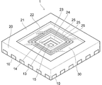
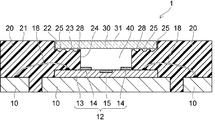
図1及び図2に示すように、本実施形態に係る光学装置1においては、基板10が設けられている。基板10は例えば銅からなり、所定の配線形状にパターニングされている。基板10上には、シリコンチップ12が設けられている。シリコンチップ12に設けられたパッド(図示せず)と基板10との間には、ワイヤ18が接続されている。なお、図1においては、ワイヤ18の図示を省略している。
As shown in FIGS. 1 and 2, the
図3に示すように、シリコンチップ12には、シリコン部分13及び金属製のガードリング14が設けられている。シリコン部分13の形状は矩形の板状である。シリコン部分13は、例えば、単結晶のシリコンからなり、シリコン部分13の上層部分の一部には、赤外線検知層15が形成されている。赤外線検知層15は、入力された赤外線を電気信号に変換する光学機能層である。上方から見て、赤外線検知層15は、シリコン部分13の中央部に配置されている。また、シリコン部分13の上層部分には、絶縁部材、配線、パッド、能動素子及び受動素子(いずれも図示せず)等の回路素子が設けられている。
As shown in FIG. 3, the
ガードリング14は、シリコン部分13の上面上に設けられており、シリコン部分13に接している。ガードリング14は、例えば銅からなり、例えばめっき法によって形成されており、その厚さは例えば数ミクロンである。上方から見て、ガードリング14の形状は、赤外線検知層15を囲む枠状である。ガードリング14の上面は、シリコン部分13の上面よりも上方にある。
The
図1及び図2に示すように、基板10上には、樹脂部材20が設けられている。樹脂部材20は樹脂材料によって一体的に形成されている。樹脂部材20の一部は、基板10におけるパターン間に配置されている。樹脂部材20の下面は基板10の下面と同一平面を構成しており、樹脂部材20の側面は基板10の側面と同一平面を構成している。ワイヤ18は樹脂部材20内に配置されている。
As shown in FIGS. 1 and 2, a
樹脂部材20の上面21の中央部には、凹部22が形成されている。凹部22の形状は例えば直方体である。凹部22の底面23の中央部には、貫通孔24が形成されている。貫通孔24の形状は例えば直方体である。貫通孔24は樹脂部材20を貫通しており、貫通孔24の底面には赤外線検知層15及びガードリング14が露出している。換言すれば、樹脂部材20の形状は赤外線検知層15を囲む枠状であり、内側面と上面の交差部分に凹部22が形成されている。凹部22の底面における貫通孔24を囲む領域には、1本又は複数本、例えば3本の溝25が形成されている。上方から見て、溝25の形状は、貫通孔24を囲み、角が丸められた矩形である。
A
樹脂部材20の凹部22内には、透明なガラス板30が設けられている。なお、「透明」には半透明も含まれる。ガラス板30の形状は、凹部22内にちょうど収納されるような矩形の板状である。ガラス板30の厚さは、凹部22の深さ以下である。このため、ガラス板30の上面31は、樹脂部材20の上面21と同じ高さか、それより下方にある。凹部22の底面とガラス板30との間には、接着剤層28が設けられている。接着剤層28の一部は、溝25内に配置されている。
A
樹脂部材20は、基板10の上面におけるシリコンチップ12が接触している領域を除く領域、基板10における各パターンの側面、シリコンチップ12の端部の上面及び側面、ワイヤ18、並びに、ガラス板30に接している。
The
樹脂部材20の貫通孔24内は、空気層40となっている。空気層40は、シリコンチップ12、樹脂部材20、及び、ガラス板30によって区画されている。空気層40には、赤外線検知層15を含むシリコン部分13の上面、ガードリング14、樹脂部材20、及び、ガラス板30が露出している。例えば、空気層40は密閉されている。光学装置1の外面は、基板10、樹脂部材20、及び、ガラス板30によって構成されている。
An
次に、本実施形態に係る光学装置の製造方法について説明する。
図4〜図7は、本実施形態に係る光学装置の製造方法を示す断面図である。
本実施形態においては、複数個の光学装置1を一括して製造する方法を例に挙げて説明する。
Next, a method for manufacturing the optical device according to the present embodiment will be described.
4 to 7 are cross-sectional views showing the method for manufacturing the optical device according to the present embodiment.
In the present embodiment, a method of collectively manufacturing a plurality of
先ず、図2に示す基板10を用意する。基板10には、シリコンチップ12を搭載する搭載領域が、複数ヶ所、マトリクス状に配列されている。また、図3に示すシリコンチップ12を複数個用意する。
First, the
次に、図4に示すように、基板10の各搭載領域上にシリコンチップ12を搭載する。そして、シリコンチップ12のパッド(図示せず)と基板10との間に、ワイヤ18を接続する。
Next, as shown in FIG. 4, the
一方、図5に示すように、治具60を用意する。治具60においては、板状の本体部62が設けられており、本体部62の下面63には、下方に向けて突出した凸部64が形成されている。凸部64の形状は直方体である。凸部64の高さは、ガラス板30の厚さ以上である。凸部64は、シリコンチップ12に対応して、複数個形成されている。凸部64の下面65の中央部には、凸部66が形成されている。凸部66の形状は直方体であり、凸部66の下面67は平坦である。また、凸部64の下面65には、レール状の微小凸部68が形成されている。微小凸部68の高さは凸部66の高さよりも低い。下方から見て、微小凸部68の形状は、凸部66を囲み、角が丸められた矩形である。
On the other hand, as shown in FIG. 5, a
そして、治具60をシリコンチップ12に当接させる。具体的には、治具60の凸部66の下面67を、シリコンチップ12のガードリング14の上面に当接させる。このとき、ガードリング14の上面は赤外線検知層15の上面よりも上方に位置しているため、治具60は赤外線検知層15には接触しない。すなわち、赤外線検知層15の上面と治具60の凸部66の下面67との間には、微小な隙間が形成される。
Then, the
次に、図6に示すように、治具60をシリコンチップ12に当接させた状態のまま、基板10と治具60との間に、流動性の樹脂材料を流入させて、充填する。このとき、銅からなるガードリング14は軟質であり、治具60との密着性が高いため、樹脂材料がガードリング14の内側まで侵入することがない。これにより、赤外線検知層15が樹脂材料によって汚染されることを回避できる。また、ガードリング14は軟質であるため、治具60をシリコンチップ12に当接させたときの衝撃を吸収し、シリコンチップ12に損傷を及ぼすことを抑制できる。
Next, as shown in FIG. 6, while the
次に、例えば加熱処理を施して、この樹脂材料を硬化させる。これにより、樹脂部材20が形成される。樹脂部材20においては、治具60の凸部64に相当する部分が凹部22となり、治具60の凸部66に相当する部分が貫通孔24となり、治具60の微小凸部68に相当する部分が溝25となる。
Next, for example, heat treatment is performed to cure the resin material. As a result, the
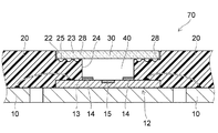
次に、図7に示すように、基板10、シリコンチップ12、ワイヤ18、及び、樹脂部材20を含む中間構造体70から、治具60(図6参照)を離隔させる。
次に、底面23に接着剤を塗布する。このとき、接着剤の一部は溝25内に進入する。
Next, as shown in FIG. 7, the jig 60 (see FIG. 6) is separated from the
Next, an adhesive is applied to the
次に、凹部22内にガラス板30を配置する。このとき、接着剤の一部が溝25内に溜められているため、ガラス板30を樹脂部材20に接着するために十分な量の接着剤を塗布しても、ガラス板30を押し付けたときに、接着剤が貫通孔24内に溢れ出すことを抑制できる。このため、接着剤の塗布量の許容範囲が広い。
Next, the
次に、接着剤を固化させて、接着剤層28を形成する。これにより、ガラス板30は、接着剤層28を介して、樹脂部材20の底面23に接着される。この結果、樹脂部材20の貫通孔24がガラス板30によって封止されて、空気層40となる。
Next, the adhesive is solidified to form the
次に、図1及び図2に示すように、基板10及び樹脂部材20をダイシングして、個片化する。これにより、複数の光学装置1が製造される。
Next, as shown in FIGS. 1 and 2, the
次に、本実施形態の効果について説明する。
本実施形態においては、図6に示す工程において、基板10に搭載されたシリコンチップ12に治具60を当接させた状態で、基板10と治具60との間に樹脂材料を充填することにより、樹脂部材20を形成している。このとき、治具60の凸部64によって凹部22が形成され、凸部66によって貫通孔24が形成され、微小凸部68によって溝25が形成される。このように、凹部22、貫通孔24及び溝25が形成された樹脂部材20を一度の工程で作製できるため、光学装置1は生産性が高い。
Next, the effect of this embodiment will be described.
In the present embodiment, in the step shown in FIG. 6, the resin material is filled between the
なお、仮に、複数の部品を組み立てることにより、樹脂部材20と同じ形状の部材を作製しようとすると、部品数が増えて部品コストが増加すると共に、精密な組立工程が必要となり、製造コストも増加する。
If a member having the same shape as that of the
また、図7に示す工程において、樹脂部材20の凹部22内にガラス板30を装入することにより、ガラス板30を自己整合的に配置することができる。このため、ガラス板30を精密に配置するための手段が不要であり、製造コストが低い。
Further, in the step shown in FIG. 7, by inserting the
更に、本実施形態においては、治具60の凸部66によって貫通孔24を形成し、樹脂部材20の凹部22内にガラス板30を配置することにより、精密な位置合わせを行うことなく、空気層40を容易に形成することができる。このため、空気層40のサイズを小さくすることができる。これにより、温度変化又は外部環境の気圧変化等に起因して、空気層40内と外部環境との間で気圧差が増大しても、ガラス板30に印加される力を抑制することができ、ガラス板30が破壊されることを抑制できる。
Further, in the present embodiment, the through
また、空気層40を小さくすることにより、ガラス板30も小さくすることができる。これにより、光学装置1のコストを低減できると共に、温度が変化したときに、樹脂部材20とガラス板30との線膨張係数の違いに起因して発生する熱応力を抑えることができる。この結果、温度変化に起因してガラス板30が破壊されることを抑制できる。
Further, the
上述の効果、すなわち、空気層40を小さくすることにより、気圧変化及び温度変化に対する耐性を高める効果は、光学装置1が自動車に搭載される場合に、特に大きい。例えば、標高の変化又は気象の変化に伴って気圧又は温度が急激に変化しても、ガラス板30が損傷することを防止できる。このため、光学装置1は信頼性が高い。
The above-described effect, that is, the effect of increasing the resistance to the atmospheric pressure change and the temperature change by reducing the
また、本実施形態においては、図5に示す工程において、治具60を軟質なガードリング14に当接させているため、シリコンチップ12に及ぼす衝撃を緩和できる。このため、治具60の当接に伴ってシリコンチップ12が損傷することを抑制できる。
Further, in this embodiment, since the
更に、治具60を軟質なガードリング14に当接させているため、治具60とガードリング14との間の密閉性が高い。このため、図6に示す工程において、樹脂材料がガードリング14の内側に侵入することを抑制できる。これにより、赤外線検知層15に入射するはずの赤外線が樹脂材料によって遮られることを抑制できる。この結果、本実施形態に係る光学装置1は、歩留まりが高い。
Furthermore, since the
更にまた、ガードリング14は、通常の配線形成プロセス、例えば、めっき法によって、形成することができる。このため、ガードリング14は形成が容易であり、形成コストが低い。
Furthermore, the
なお、仮に、ガードリング14を設けないと、流動性の樹脂材料が赤外線検知層15に到達することを阻止するための阻止部材が必要となる。しかしながら、このような阻止部材を設けると、部品数が増加して部品コストが増加すると共に、阻止部材を適切な位置に配置する工程が必要となるため、製造コストも増加する。
If the
更にまた、本実施形態においては、底面23に溝25が形成されている。このため、図7に示す工程において、底面23に接着剤を塗布するときに、接着剤の一部を溝25内に溜めることができる。これにより、ガラス板30を樹脂部材20に接着するために十分な量の接着剤を塗布しても、接着剤が貫通孔24内に溢れ出すことを抑制できる。従って、本実施形態によれば、ガラス板30の接着強度を確保できると共に、接着剤の塗布量の許容範囲が広く、光学装置1の製造が容易である。
Furthermore, in this embodiment, the
更にまた、本実施形態においては、ガラス板30の厚さが凹部22の深さ以下であるため、ガラス板30が樹脂部材20の上面21から突出しない。これにより、人が光学装置1に触れたときに、ガラス板30のエッジによって指先を損傷する可能性が低い。なお、仮に、ガラス板30を樹脂部材20の上面21から突出させる場合は、ガラス板30のエッジに対して面取り加工が必要となり、コストが増加する。
Furthermore, in the present embodiment, since the thickness of the
なお、本実施形態においては、光学装置1が赤外線センサである例を示したが、これには限定されない。光学装置1は、例えば、可視光センサであってもよく、紫外線センサであってもよい。また、光学装置1は、発光装置であってもよい。
In the present embodiment, the example in which the
以上説明した実施形態によれば、コストの低下を可能とする光学装置及びその製造方法を実現することができる。 According to the embodiments described above, it is possible to realize the optical device and the manufacturing method thereof that can reduce the cost.
以上、本発明のいくつかの実施形態を説明したが、これらの実施形態は、例として提示したものであり、発明の範囲を限定することは意図していない。これら新規な実施形態は、その他の様々な形態で実施されることが可能であり、発明の要旨を逸脱しない範囲で、種々の省略、置き換え、変更を行うことができる。これら実施形態やその変形は、発明の範囲や要旨に含まれるとともに、特許請求の範囲に記載された発明及びその等価物の範囲に含まれる。 Although some embodiments of the present invention have been described above, these embodiments are presented as examples and are not intended to limit the scope of the invention. These novel embodiments can be implemented in various other forms, and various omissions, replacements, and changes can be made without departing from the spirit of the invention. These embodiments and their modifications are included in the scope and gist of the invention, and are also included in the scope of the invention described in the claims and the equivalents thereof.
1:光学装置、10:基板、12:シリコンチップ、13:シリコン部分、14:ガードリング、15:赤外線検知層、18:ワイヤ、20:樹脂部材、21:上面、22:凹部、23:底面、24:貫通孔、25:溝、28:接着剤層、30:ガラス板、31:上面、40:空気層、60:治具、62:本体部、63:下面、64:凸部、65:下面、66:凸部、67:下面、68:微小凸部、70:中間構造体 1: Optical device, 10: Substrate, 12: Silicon chip, 13: Silicon part, 14: Guard ring, 15: Infrared detection layer, 18: Wire, 20: Resin member, 21: Top surface, 22: Recessed portion, 23: Bottom surface , 24: through hole, 25: groove, 28: adhesive layer, 30: glass plate, 31: upper surface, 40: air layer, 60: jig, 62: body portion, 63: lower surface, 64: convex portion, 65 : Lower surface, 66: convex portion, 67: lower surface, 68: minute convex portion, 70: intermediate structure
Claims (7)
前記基板上に設けられ、上層部分の一部に光学機能層が形成された半導体チップと、
前記基板上に設けられ、前記光学機能層を囲む枠状であり、内側面と上面の交差部分に凹部が形成され、樹脂材料により一体的に形成された樹脂部材と、
前記凹部内に配置された透明板と、
を備え、
前記半導体チップ、前記樹脂部材及び前記透明板によって空気層が区画されており、
前記半導体チップは、
前記光学機能層が形成された半導体部分と、
前記半導体部分の上面上に設けられ、上方から見て前記光学機能層を囲み、金属からなるガードリングと、
を有し、
前記ガードリングは前記樹脂部材に接し、前記空気層に露出している光学装置。 Board,
A semiconductor chip provided on the substrate, in which an optical functional layer is formed in a part of the upper layer portion,
A resin member which is provided on the substrate, has a frame shape surrounding the optical functional layer, and has a concave portion formed at an intersection of an inner side surface and an upper surface, and which is integrally formed of a resin material,
A transparent plate arranged in the recess,
Equipped with
An air layer is partitioned by the semiconductor chip, the resin member and the transparent plate ,
The semiconductor chip is
A semiconductor portion on which the optical functional layer is formed,
A guard ring that is provided on the upper surface of the semiconductor portion, surrounds the optical functional layer when viewed from above, and is made of metal,
Have
An optical device in which the guard ring is in contact with the resin member and is exposed to the air layer .
前記凹部の底面には溝が形成されており、
前記接着剤層の一部は前記溝内に配置されている請求項1記載の光学装置。 Further comprising an adhesive layer for adhering the transparent plate to the resin member,
A groove is formed on the bottom surface of the recess,
Wherein a portion of the adhesive layer is an optical device according to claim 1, characterized in that disposed in the groove.
本体部の下面に第1凸部が形成され、前記第1凸部の下面に第2凸部が形成された治具の前記第2凸部を、前記半導体チップの上面における前記光学機能層を囲む領域に当接させる工程と、
前記治具を前記半導体チップに当接させた状態のまま、前記基板と前記治具との間に流動性の樹脂材料を充填する工程と、
前記樹脂材料を硬化させることにより、樹脂部材を形成する工程と、
前記基板、前記半導体チップ及び前記樹脂部材から、前記治具を離隔させる工程と、
前記樹脂部材における前記第1凸部に対応する凹部内に、透明板を配置する工程と、
を備え、
前記半導体チップは、前記光学機能層が形成された半導体部分、及び、前記半導体部分の上面上に設けられ、前記光学機能層を囲み、金属からなるガードリングを含み、
前記当接させる工程において、前記第2凸部を前記ガードリングに当接させ、
前記樹脂材料を充填する工程において、前記樹脂材料を前記ガードリングの内側には侵入させない光学装置の製造方法。 On the substrate, a step of mounting a semiconductor chip having an optical functional layer formed in a part of the upper layer portion,
The first convex portion is formed on the lower surface of the main body portion, and the second convex portion of the jig, in which the second convex portion is formed on the lower surface of the first convex portion, Contacting the surrounding area,
Filling a fluid resin material between the substrate and the jig while keeping the jig in contact with the semiconductor chip,
A step of forming a resin member by curing the resin material,
A step of separating the jig from the substrate, the semiconductor chip and the resin member,
Arranging a transparent plate in a concave portion of the resin member corresponding to the first convex portion;
Equipped with
The semiconductor chip includes a semiconductor portion on which the optical functional layer is formed, and a guard ring that is provided on the upper surface of the semiconductor portion, surrounds the optical functional layer, and is made of metal.
In the step of contacting, contacting the second convex portion with the guard ring,
A method of manufacturing an optical device , wherein in the step of filling the resin material, the resin material is prevented from entering the inside of the guard ring .
前記治具の前記第1凸部の下面における前記第2凸部を囲む領域には、前記第2凸部よりも低い第3凸部が形成されている請求項6に記載の光学装置の製造方法。 Between the step of separating the jig and the step of disposing the transparent plate, the method further comprises a step of applying an adhesive on the bottom surface of the recess of the resin member,
The manufacturing of the optical device according to claim 6 , wherein a third convex portion lower than the second convex portion is formed in a region surrounding the second convex portion on the lower surface of the first convex portion of the jig. Method.
Priority Applications (2)
| Application Number | Priority Date | Filing Date | Title |
|---|---|---|---|
| JP2017029924A JP6730948B2 (en) | 2017-02-21 | 2017-02-21 | Optical device and manufacturing method thereof |
| US15/698,840 US10347685B2 (en) | 2017-02-21 | 2017-09-08 | Optical device and method for manufacturing same |
Applications Claiming Priority (1)
| Application Number | Priority Date | Filing Date | Title |
|---|---|---|---|
| JP2017029924A JP6730948B2 (en) | 2017-02-21 | 2017-02-21 | Optical device and manufacturing method thereof |
Publications (3)
| Publication Number | Publication Date |
|---|---|
| JP2018136171A JP2018136171A (en) | 2018-08-30 |
| JP2018136171A5 JP2018136171A5 (en) | 2019-03-28 |
| JP6730948B2 true JP6730948B2 (en) | 2020-07-29 |
Family
ID=63167980
Family Applications (1)
| Application Number | Title | Priority Date | Filing Date |
|---|---|---|---|
| JP2017029924A Active JP6730948B2 (en) | 2017-02-21 | 2017-02-21 | Optical device and manufacturing method thereof |
Country Status (2)
| Country | Link |
|---|---|
| US (1) | US10347685B2 (en) |
| JP (1) | JP6730948B2 (en) |
Families Citing this family (2)
| Publication number | Priority date | Publication date | Assignee | Title |
|---|---|---|---|---|
| JP6840644B2 (en) * | 2017-09-05 | 2021-03-10 | 株式会社東芝 | Semiconductor device |
| US11784102B2 (en) * | 2020-07-29 | 2023-10-10 | UTAC Headquarters Pte. Ltd. | Hermetic semiconductor packages |
Family Cites Families (7)
| Publication number | Priority date | Publication date | Assignee | Title |
|---|---|---|---|---|
| US6525405B1 (en) * | 2000-03-30 | 2003-02-25 | Alphatec Holding Company Limited | Leadless semiconductor product packaging apparatus having a window lid and method for packaging |
| TWI251886B (en) * | 2004-11-03 | 2006-03-21 | Advanced Semiconductor Eng | Sensor chip for defining molding exposed region and method for manufacturing the same |
| JP2006145501A (en) | 2004-11-24 | 2006-06-08 | Hamamatsu Photonics Kk | Infrared radiation detecting device |
| US7582954B1 (en) * | 2008-02-25 | 2009-09-01 | National Semiconductor Corporation | Optical leadless leadframe package |
| KR101531129B1 (en) * | 2014-02-07 | 2015-06-23 | 삼성전기주식회사 | MEMS Microphone |
| US9355870B1 (en) * | 2015-01-15 | 2016-05-31 | Silicon Laboratories Inc. | Integrated circuit with sensor area and resin dam |
| US9722098B1 (en) * | 2016-10-18 | 2017-08-01 | Ase Electronics (M) Sdn Bhd | Semiconductor device package and method of manufacturing the same |
-
2017
- 2017-02-21 JP JP2017029924A patent/JP6730948B2/en active Active
- 2017-09-08 US US15/698,840 patent/US10347685B2/en active Active
Also Published As
| Publication number | Publication date |
|---|---|
| US10347685B2 (en) | 2019-07-09 |
| JP2018136171A (en) | 2018-08-30 |
| US20180240839A1 (en) | 2018-08-23 |
Similar Documents
| Publication | Publication Date | Title |
|---|---|---|
| US7457490B2 (en) | Micro-optics on optoelectronics | |
| CN107591420B (en) | Sensor package structure | |
| US10566760B2 (en) | Light emitting device | |
| CN101159279A (en) | Semiconductor image sensor die and production method thereof, semiconductor image sensor module, image sensor device, optical device element, and optical device module | |
| US9327457B2 (en) | Electronic device and method for manufacturing electronic device | |
| JP2013004534A (en) | Semiconductor package | |
| US20120286437A1 (en) | Electronic device and method of manufacturing the electronic device | |
| WO2017208724A1 (en) | Optical module, module, and methods for manufacturing optical module and module | |
| JP6730948B2 (en) | Optical device and manufacturing method thereof | |
| JP4782522B2 (en) | Optical functional device package and manufacturing method thereof | |
| TWI745575B (en) | Semiconductor device package and a method of manufacturing the same | |
| KR102126418B1 (en) | Image sensor package | |
| JP6005779B2 (en) | LIGHT EMITTING DEVICE, LIGHT EMITTING DEVICE MANUFACTURING METHOD, AND OPTICAL DEVICE | |
| US10573677B2 (en) | Semiconductor device on which a transparent plate is disposed for exposing an element region | |
| JP6162284B2 (en) | Light emitting device | |
| US20190339478A1 (en) | Optical device | |
| JP2014179470A (en) | Packaging structure of image sensor | |
| JP6889452B1 (en) | Image sensor module and manufacturing method of image sensor module | |
| KR101364020B1 (en) | Semiconductor package and the fabriation method thereof | |
| KR20160070514A (en) | Sensor package and manufacturing method thereof | |
| KR20090116970A (en) | Wafer lever lens portion and light emitting device package using the same | |
| JP5838142B2 (en) | Semiconductor device and manufacturing method thereof | |
| US20220109282A1 (en) | Method for obtaining electronic devices and electronic devices | |
| CN117913149A (en) | Sensor package structure and manufacturing method thereof | |
| WO2010143389A1 (en) | Semiconductor device |
Legal Events
| Date | Code | Title | Description |
|---|---|---|---|
| A711 | Notification of change in applicant |
Free format text: JAPANESE INTERMEDIATE CODE: A712 Effective date: 20170911 |
|
| A711 | Notification of change in applicant |
Free format text: JAPANESE INTERMEDIATE CODE: A711 Effective date: 20170912 |
|
| A521 | Request for written amendment filed |
Free format text: JAPANESE INTERMEDIATE CODE: A523 Effective date: 20171031 |
|
| A521 | Request for written amendment filed |
Free format text: JAPANESE INTERMEDIATE CODE: A523 Effective date: 20190204 |
|
| A621 | Written request for application examination |
Free format text: JAPANESE INTERMEDIATE CODE: A621 Effective date: 20190204 |
|
| A977 | Report on retrieval |
Free format text: JAPANESE INTERMEDIATE CODE: A971007 Effective date: 20191120 |
|
| A131 | Notification of reasons for refusal |
Free format text: JAPANESE INTERMEDIATE CODE: A131 Effective date: 20191203 |
|
| A521 | Request for written amendment filed |
Free format text: JAPANESE INTERMEDIATE CODE: A523 Effective date: 20200131 |
|
| TRDD | Decision of grant or rejection written | ||
| A01 | Written decision to grant a patent or to grant a registration (utility model) |
Free format text: JAPANESE INTERMEDIATE CODE: A01 Effective date: 20200603 |
|
| A61 | First payment of annual fees (during grant procedure) |
Free format text: JAPANESE INTERMEDIATE CODE: A61 Effective date: 20200703 |
|
| R150 | Certificate of patent or registration of utility model |
Ref document number: 6730948 Country of ref document: JP Free format text: JAPANESE INTERMEDIATE CODE: R150 |