JP6713720B2 - Light emitting device package and vehicle lighting device including the same - Google Patents
Light emitting device package and vehicle lighting device including the same Download PDFInfo
- Publication number
- JP6713720B2 JP6713720B2 JP2014173374A JP2014173374A JP6713720B2 JP 6713720 B2 JP6713720 B2 JP 6713720B2 JP 2014173374 A JP2014173374 A JP 2014173374A JP 2014173374 A JP2014173374 A JP 2014173374A JP 6713720 B2 JP6713720 B2 JP 6713720B2
- Authority
- JP
- Japan
- Prior art keywords
- light emitting
- light
- cells
- emitting cells
- cell
- Prior art date
- Legal status (The legal status is an assumption and is not a legal conclusion. Google has not performed a legal analysis and makes no representation as to the accuracy of the status listed.)
- Active
Links
Images


Classifications
-
- H—ELECTRICITY
- H01—ELECTRIC ELEMENTS
- H01L—SEMICONDUCTOR DEVICES NOT COVERED BY CLASS H10
- H01L33/00—Semiconductor devices with at least one potential-jump barrier or surface barrier specially adapted for light emission; Processes or apparatus specially adapted for the manufacture or treatment thereof or of parts thereof; Details thereof
- H01L33/02—Semiconductor devices with at least one potential-jump barrier or surface barrier specially adapted for light emission; Processes or apparatus specially adapted for the manufacture or treatment thereof or of parts thereof; Details thereof characterised by the semiconductor bodies
- H01L33/08—Semiconductor devices with at least one potential-jump barrier or surface barrier specially adapted for light emission; Processes or apparatus specially adapted for the manufacture or treatment thereof or of parts thereof; Details thereof characterised by the semiconductor bodies with a plurality of light emitting regions, e.g. laterally discontinuous light emitting layer or photoluminescent region integrated within the semiconductor body
-
- H—ELECTRICITY
- H01—ELECTRIC ELEMENTS
- H01L—SEMICONDUCTOR DEVICES NOT COVERED BY CLASS H10
- H01L25/00—Assemblies consisting of a plurality of individual semiconductor or other solid state devices ; Multistep manufacturing processes thereof
- H01L25/03—Assemblies consisting of a plurality of individual semiconductor or other solid state devices ; Multistep manufacturing processes thereof all the devices being of a type provided for in the same subgroup of groups H01L27/00 - H01L33/00, or in a single subclass of H10K, H10N, e.g. assemblies of rectifier diodes
- H01L25/04—Assemblies consisting of a plurality of individual semiconductor or other solid state devices ; Multistep manufacturing processes thereof all the devices being of a type provided for in the same subgroup of groups H01L27/00 - H01L33/00, or in a single subclass of H10K, H10N, e.g. assemblies of rectifier diodes the devices not having separate containers
- H01L25/075—Assemblies consisting of a plurality of individual semiconductor or other solid state devices ; Multistep manufacturing processes thereof all the devices being of a type provided for in the same subgroup of groups H01L27/00 - H01L33/00, or in a single subclass of H10K, H10N, e.g. assemblies of rectifier diodes the devices not having separate containers the devices being of a type provided for in group H01L33/00
- H01L25/0753—Assemblies consisting of a plurality of individual semiconductor or other solid state devices ; Multistep manufacturing processes thereof all the devices being of a type provided for in the same subgroup of groups H01L27/00 - H01L33/00, or in a single subclass of H10K, H10N, e.g. assemblies of rectifier diodes the devices not having separate containers the devices being of a type provided for in group H01L33/00 the devices being arranged next to each other
-
- F—MECHANICAL ENGINEERING; LIGHTING; HEATING; WEAPONS; BLASTING
- F21—LIGHTING
- F21K—NON-ELECTRIC LIGHT SOURCES USING LUMINESCENCE; LIGHT SOURCES USING ELECTROCHEMILUMINESCENCE; LIGHT SOURCES USING CHARGES OF COMBUSTIBLE MATERIAL; LIGHT SOURCES USING SEMICONDUCTOR DEVICES AS LIGHT-GENERATING ELEMENTS; LIGHT SOURCES NOT OTHERWISE PROVIDED FOR
- F21K9/00—Light sources using semiconductor devices as light-generating elements, e.g. using light-emitting diodes [LED] or lasers
- F21K9/60—Optical arrangements integrated in the light source, e.g. for improving the colour rendering index or the light extraction
-
- F—MECHANICAL ENGINEERING; LIGHTING; HEATING; WEAPONS; BLASTING
- F21—LIGHTING
- F21S—NON-PORTABLE LIGHTING DEVICES; SYSTEMS THEREOF; VEHICLE LIGHTING DEVICES SPECIALLY ADAPTED FOR VEHICLE EXTERIORS
- F21S43/00—Signalling devices specially adapted for vehicle exteriors, e.g. brake lamps, direction indicator lights or reversing lights
- F21S43/20—Signalling devices specially adapted for vehicle exteriors, e.g. brake lamps, direction indicator lights or reversing lights characterised by refractors, transparent cover plates, light guides or filters
- F21S43/26—Refractors, transparent cover plates, light guides or filters not provided in groups F21S43/235 - F21S43/255
-
- H—ELECTRICITY
- H01—ELECTRIC ELEMENTS
- H01L—SEMICONDUCTOR DEVICES NOT COVERED BY CLASS H10
- H01L27/00—Devices consisting of a plurality of semiconductor or other solid-state components formed in or on a common substrate
- H01L27/15—Devices consisting of a plurality of semiconductor or other solid-state components formed in or on a common substrate including semiconductor components with at least one potential-jump barrier or surface barrier specially adapted for light emission
- H01L27/153—Devices consisting of a plurality of semiconductor or other solid-state components formed in or on a common substrate including semiconductor components with at least one potential-jump barrier or surface barrier specially adapted for light emission in a repetitive configuration, e.g. LED bars
- H01L27/156—Devices consisting of a plurality of semiconductor or other solid-state components formed in or on a common substrate including semiconductor components with at least one potential-jump barrier or surface barrier specially adapted for light emission in a repetitive configuration, e.g. LED bars two-dimensional arrays
-
- H—ELECTRICITY
- H01—ELECTRIC ELEMENTS
- H01L—SEMICONDUCTOR DEVICES NOT COVERED BY CLASS H10
- H01L33/00—Semiconductor devices with at least one potential-jump barrier or surface barrier specially adapted for light emission; Processes or apparatus specially adapted for the manufacture or treatment thereof or of parts thereof; Details thereof
- H01L33/48—Semiconductor devices with at least one potential-jump barrier or surface barrier specially adapted for light emission; Processes or apparatus specially adapted for the manufacture or treatment thereof or of parts thereof; Details thereof characterised by the semiconductor body packages
- H01L33/50—Wavelength conversion elements
-
- H—ELECTRICITY
- H01—ELECTRIC ELEMENTS
- H01L—SEMICONDUCTOR DEVICES NOT COVERED BY CLASS H10
- H01L2224/00—Indexing scheme for arrangements for connecting or disconnecting semiconductor or solid-state bodies and methods related thereto as covered by H01L24/00
- H01L2224/01—Means for bonding being attached to, or being formed on, the surface to be connected, e.g. chip-to-package, die-attach, "first-level" interconnects; Manufacturing methods related thereto
- H01L2224/42—Wire connectors; Manufacturing methods related thereto
- H01L2224/47—Structure, shape, material or disposition of the wire connectors after the connecting process
- H01L2224/48—Structure, shape, material or disposition of the wire connectors after the connecting process of an individual wire connector
- H01L2224/4805—Shape
- H01L2224/4809—Loop shape
- H01L2224/48091—Arched
-
- H—ELECTRICITY
- H01—ELECTRIC ELEMENTS
- H01L—SEMICONDUCTOR DEVICES NOT COVERED BY CLASS H10
- H01L2224/00—Indexing scheme for arrangements for connecting or disconnecting semiconductor or solid-state bodies and methods related thereto as covered by H01L24/00
- H01L2224/01—Means for bonding being attached to, or being formed on, the surface to be connected, e.g. chip-to-package, die-attach, "first-level" interconnects; Manufacturing methods related thereto
- H01L2224/42—Wire connectors; Manufacturing methods related thereto
- H01L2224/47—Structure, shape, material or disposition of the wire connectors after the connecting process
- H01L2224/48—Structure, shape, material or disposition of the wire connectors after the connecting process of an individual wire connector
- H01L2224/481—Disposition
- H01L2224/48151—Connecting between a semiconductor or solid-state body and an item not being a semiconductor or solid-state body, e.g. chip-to-substrate, chip-to-passive
- H01L2224/48221—Connecting between a semiconductor or solid-state body and an item not being a semiconductor or solid-state body, e.g. chip-to-substrate, chip-to-passive the body and the item being stacked
- H01L2224/48225—Connecting between a semiconductor or solid-state body and an item not being a semiconductor or solid-state body, e.g. chip-to-substrate, chip-to-passive the body and the item being stacked the item being non-metallic, e.g. insulating substrate with or without metallisation
- H01L2224/48227—Connecting between a semiconductor or solid-state body and an item not being a semiconductor or solid-state body, e.g. chip-to-substrate, chip-to-passive the body and the item being stacked the item being non-metallic, e.g. insulating substrate with or without metallisation connecting the wire to a bond pad of the item
-
- H—ELECTRICITY
- H01—ELECTRIC ELEMENTS
- H01L—SEMICONDUCTOR DEVICES NOT COVERED BY CLASS H10
- H01L2224/00—Indexing scheme for arrangements for connecting or disconnecting semiconductor or solid-state bodies and methods related thereto as covered by H01L24/00
- H01L2224/73—Means for bonding being of different types provided for in two or more of groups H01L2224/10, H01L2224/18, H01L2224/26, H01L2224/34, H01L2224/42, H01L2224/50, H01L2224/63, H01L2224/71
- H01L2224/732—Location after the connecting process
- H01L2224/73251—Location after the connecting process on different surfaces
- H01L2224/73265—Layer and wire connectors
-
- H—ELECTRICITY
- H01—ELECTRIC ELEMENTS
- H01L—SEMICONDUCTOR DEVICES NOT COVERED BY CLASS H10
- H01L33/00—Semiconductor devices with at least one potential-jump barrier or surface barrier specially adapted for light emission; Processes or apparatus specially adapted for the manufacture or treatment thereof or of parts thereof; Details thereof
- H01L33/02—Semiconductor devices with at least one potential-jump barrier or surface barrier specially adapted for light emission; Processes or apparatus specially adapted for the manufacture or treatment thereof or of parts thereof; Details thereof characterised by the semiconductor bodies
- H01L33/20—Semiconductor devices with at least one potential-jump barrier or surface barrier specially adapted for light emission; Processes or apparatus specially adapted for the manufacture or treatment thereof or of parts thereof; Details thereof characterised by the semiconductor bodies with a particular shape, e.g. curved or truncated substrate
-
- H—ELECTRICITY
- H01—ELECTRIC ELEMENTS
- H01L—SEMICONDUCTOR DEVICES NOT COVERED BY CLASS H10
- H01L33/00—Semiconductor devices with at least one potential-jump barrier or surface barrier specially adapted for light emission; Processes or apparatus specially adapted for the manufacture or treatment thereof or of parts thereof; Details thereof
- H01L33/48—Semiconductor devices with at least one potential-jump barrier or surface barrier specially adapted for light emission; Processes or apparatus specially adapted for the manufacture or treatment thereof or of parts thereof; Details thereof characterised by the semiconductor body packages
- H01L33/50—Wavelength conversion elements
- H01L33/501—Wavelength conversion elements characterised by the materials, e.g. binder
- H01L33/502—Wavelength conversion materials
- H01L33/504—Elements with two or more wavelength conversion materials
-
- H—ELECTRICITY
- H01—ELECTRIC ELEMENTS
- H01L—SEMICONDUCTOR DEVICES NOT COVERED BY CLASS H10
- H01L33/00—Semiconductor devices with at least one potential-jump barrier or surface barrier specially adapted for light emission; Processes or apparatus specially adapted for the manufacture or treatment thereof or of parts thereof; Details thereof
- H01L33/48—Semiconductor devices with at least one potential-jump barrier or surface barrier specially adapted for light emission; Processes or apparatus specially adapted for the manufacture or treatment thereof or of parts thereof; Details thereof characterised by the semiconductor body packages
- H01L33/50—Wavelength conversion elements
- H01L33/508—Wavelength conversion elements having a non-uniform spatial arrangement or non-uniform concentration, e.g. patterned wavelength conversion layer, wavelength conversion layer with a concentration gradient of the wavelength conversion material
Description
本発明は、発光素子パッケージ及びそれを含む車両用照明装置に関する。 The present invention relates to a light emitting device package and a vehicle lighting device including the same.
半導体の3−5族または2−6族化合物半導体物質を用いた発光ダイオード(Light Emitting Diode:LED)やレーザーダイオード(Laser Diode:LD)のような発光素子は、薄膜成長技術及び素子材料の開発によって赤色、緑色、青色及び紫外線などの様々な色を具現することができ、蛍光物質を用いたり、色を組み合わせたりすることによって効率の良い白色光線も具現可能であり、蛍光灯、白熱灯などの既存の光源に比べて低消費電力、半永久的な寿命、速い応答速度、安全性、環境親和性などの長所を有する。 A light emitting device such as a light emitting diode (LED) or a laser diode (laser diode: LD) using a semiconductor semiconductor group 3-5 or 2-6 compound semiconductor material is a thin film growth technology and development of a device material. Various colors such as red, green, blue and ultraviolet can be realized by using it, and efficient white light can also be realized by using fluorescent substances or combining colors, such as fluorescent lamps and incandescent lamps. Compared with existing light sources, it has advantages such as low power consumption, semi-permanent life, fast response speed, safety, and environmental friendliness.
したがって、発光ダイオードは、光通信手段の送信モジュール、LCD(Liquid Crystal Display)表示装置のバックライトを構成する冷陰極管(CCFL:Cold Cathode Fluorescence Lamp)を代替する発光ダイオードバックライト、蛍光灯や白熱電球を代替することができる白色発光ダイオード照明装置、自動車のヘッドライト及び信号灯にまでその応用が拡大されている。 Therefore, the light emitting diode is a light emitting diode backlight that replaces a cold cathode tube (CCFL: Cold Cathode Fluorescence Lamp) that constitutes a transmission module of optical communication means, a backlight of an LCD (Liquid Crystal Display) device, a fluorescent lamp or an incandescent lamp. Its applications have been expanded to white light emitting diode lighting devices that can replace light bulbs, automobile headlights, and signal lights.
発光素子は、サファイアなどからなる基板上に、第1導電型半導体層、活性層及び第2導電型半導体層を含む発光構造物が形成され、第1導電型半導体層と第2導電型半導体層上にそれぞれ第1電極と第2電極が配置される。 In the light emitting device, a light emitting structure including a first conductive type semiconductor layer, an active layer and a second conductive type semiconductor layer is formed on a substrate made of sapphire, the first conductive type semiconductor layer and the second conductive type semiconductor layer. A first electrode and a second electrode are respectively disposed on the top.
発光素子パッケージは、パッケージボディーに第1電極及び第2電極が配置され、パッケージボディーの底面に発光素子が配置され、第1電極及び第2電極と電気的に接続される。 In the light emitting device package, the first electrode and the second electrode are disposed on the package body, the light emitting device is disposed on the bottom surface of the package body, and are electrically connected to the first electrode and the second electrode.
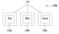
図1A及び図1Bは、従来の発光素子パッケージを示す図である。 1A and 1B are views showing a conventional light emitting device package.
複数個の発光素子150a,150b,150cが配置された発光素子パッケージ100の場合、基板110上にそれぞれの発光素子150a,150b,150cが所定間隔離隔して配置されており、それぞれの発光素子150a,150b,150cは、同じ波長領域の光を放出するか、または異なる波長領域の光を放出することができる。
In the case of the light
例えば、発光素子パッケージから白色光を放出しようとする場合、図1Aに示すように、一つの基板110に互いに異なる波長領域の光(Red、Blue、Green)を放出する3つの発光素子150a,150b,150cを配置するか、または互いに異なる基板110にそれぞれ互いに異なる波長領域の光(Red、Blue、Green)を放出する3つの発光素子150a,150b,150cを配置してもよい。
For example, when white light is emitted from a light emitting device package, as shown in FIG. 1A, three
このとき、3つの発光素子150a,150b,150cは、活性層から互いに異なる波長領域の光を放出するか、または、活性層から同じ波長領域の光を放出するとしても、互いに異なる種類の蛍光体を配置することができる。
At this time, the three
上述したように、一つの発光素子パッケージ内に互いに異なる波長領域の光を放出する複数個の発光素子を使用する場合、デザインの制約ないしコストの上昇を予想することができる。 As described above, when using a plurality of light emitting devices that emit light of different wavelength regions in one light emitting device package, design restrictions or cost increase can be expected.
特に、車両用後方照明装置のように、狭い空間内で様々な色相ないし形状の光を放出しようとするとき、互いに異なる光を放出するそれぞれの発光素子を隣接するように配置するのに技術的な限界があり得る。 In particular, when it is intended to emit light of various hues or shapes in a narrow space, such as a vehicle rear lighting device, it is technically necessary to arrange light emitting elements that emit different light so as to be adjacent to each other. There can be limits.
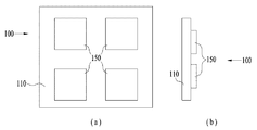
そして、図2Aは、従来の発光素子パッケージを示す図である。 2A is a view showing a conventional light emitting device package.
複数個の発光素子150が配置された発光素子パッケージ100の場合、基板110上にそれぞれの発光素子150が所定間隔離隔して配置されており、それぞれの発光素子150は、同じ波長領域の光を放出するか、または異なる波長領域の光を放出することができる。
In the case of the light
図2Bは、従来の光源モジュールを示す図である。 FIG. 2B is a diagram showing a conventional light source module.
光源モジュールにおいて、発光素子パッケージの前方にレンズ180が配置されて、基板110上のそれぞれの発光素子150から放出された光の進行経路を変更させることができる。特に、車両用照明装置に使用されるとき、レンズ180として非球面のレンズが使用され、発光素子150の発光形状がそのまま伝達されるので、発光素子150の光源の形状が重要であり得る。
In the light source module, the
しかし、通常、発光素子の光源の形状は正方形又は長方形であるため、外部に伝達される光の形状の具現に制約がある。また、それぞれの発光素子を隣接するように配置するのに技術的な限界があり得る。 However, since the shape of the light source of the light emitting element is usually a square or a rectangle, there is a limitation in realizing the shape of light transmitted to the outside. In addition, there may be a technical limitation in arranging the respective light emitting elements so as to be adjacent to each other.
本発明に係る様々な実施形態により、発光素子パッケージ及びそれを含む車両用照明装置において、光源の配置の自由度を増加させ、光源から外部に伝達される光の形状を多様化し、製造コストを低減する。 According to various embodiments of the present invention, in a light emitting device package and a vehicle lighting device including the same, the degree of freedom of arrangement of the light source is increased, the shape of light transmitted from the light source to the outside is diversified, and the manufacturing cost is reduced. Reduce.
本発明の一実施形態によると、パッケージボディーと;前記パッケージボディー上に配置され、第1導電型半導体層、活性層及び第2導電型半導体層を含み、少なくとも2つの発光セル(cell)に分かれた発光構造物と;前記パッケージボディーと前記発光構造物との間に位置する支持基板と:前記それぞれの発光セルに接続された第1電極及び第2電極と;前記それぞれの発光セル上に配置された蛍光体と;を含み、互いに隣接する発光セルは、前記第1導電型半導体層、前記活性層及び前記第2導電型半導体層のうち少なくとも2層以上が電気的に分離される発光素子パッケージを提供する。 According to an embodiment of the present invention, a package body; disposed on the package body, including a first conductive type semiconductor layer, an active layer and a second conductive type semiconductor layer, and divided into at least two light emitting cells. A light emitting structure; a supporting substrate located between the package body and the light emitting structure; a first electrode and a second electrode connected to the respective light emitting cells; arranged on the respective light emitting cells And a light emitting element in which at least two layers of the first conductive type semiconductor layer, the active layer and the second conductive type semiconductor layer are electrically separated from each other in the light emitting cells adjacent to each other. Provide the package.
それぞれの発光セルは、互いに同じ波長領域の光を放出し、前記それぞれの発光セル上に配置された蛍光体のうち少なくとも一部は、互いに異なる波長領域の光を放出することができる。 Each of the light emitting cells emits light in the same wavelength region, and at least a part of the phosphors arranged on the respective light emitting cells can emit light in different wavelength regions.
それぞれの発光セルは、一つの発光構造物が成長した後、前記成長した一つの発光構造物がエッチングされることにより分かれてもよい。 Each light emitting cell may be separated by growing one light emitting structure and then etching the grown one light emitting structure.
蛍光体は、コンフォーマルコーティングされるか、またはフィルムタイプで配置されてもよい。 The phosphors may be conformally coated or arranged in film type.
隣接する前記発光セル間の距離は10μm〜50μmであってもよい。 The distance between the adjacent light emitting cells may be 10 μm to 50 μm.
発光素子パッケージは、発光構造物が配置された基板をさらに含み、前記それぞれの発光セルは、メサエッチングされて第2導電型半導体層から活性層及び第1導電型半導体層の一部がエッチングされることにより、前記第1導電型半導体層の一部が露出され、前記それぞれの領域の発光セルの第2導電型半導体層と露出された第1導電型半導体層上にそれぞれ、第2電極と第1電極を配置することができる。 The light emitting device package further includes a substrate on which the light emitting structure is disposed, and each of the light emitting cells is mesa-etched to partially etch the active layer and the first conductive type semiconductor layer from the second conductive type semiconductor layer. As a result, a part of the first conductive type semiconductor layer is exposed, and a second electrode is formed on the second conductive type semiconductor layer of the light emitting cell in each of the regions and the exposed first conductive type semiconductor layer. A first electrode can be placed.
発光素子パッケージは、発光構造物が配置された導電性支持基板をさらに含み、前記それぞれの発光セルの第1導電型半導体層上にそれぞれ第1電極を配置することができる。 The light emitting device package may further include a conductive support substrate on which the light emitting structure is disposed, and the first electrodes may be disposed on the first conductive type semiconductor layers of the respective light emitting cells.
本発明の他の実施形態によると、回路基板と;前記回路基板上に配置された上述した発光素子パッケージと;前記発光素子パッケージ上に配置されたレンズと;を含み、前記発光構造物は、少なくとも2つ以上配置され、前記それぞれの発光構造物は青色波長領域の光を放出し、前記それぞれの発光セルには黄色蛍光体と赤色蛍光体とが少なくとも配置された車両用照明装置を提供する。 According to another exemplary embodiment of the present invention, the light emitting structure includes a circuit board; the light emitting device package described above disposed on the circuit board; and a lens disposed on the light emitting device package. Provided is a lighting device for a vehicle, wherein at least two or more of the light emitting structures emit light in a blue wavelength region, and at least yellow phosphors and red phosphors are arranged in the respective light emitting cells. ..
それぞれの発光構造物は、黄色蛍光体が配置された第1発光セルと、赤色蛍光体が配置された第2発光セルとを含み、前記それぞれの発光構造物内の第1発光セルと第2発光セルとは同一に配列されてもよい。 Each of the light emitting structures includes a first light emitting cell in which a yellow phosphor is disposed and a second light emitting cell in which a red phosphor is disposed, and the first light emitting cell and the second light emitting cell in each of the light emitting structures. The light emitting cells may be arranged in the same manner.
第1発光セルと第2発光セルは互いに独立して駆動可能である。 The first light emitting cell and the second light emitting cell can be driven independently of each other.
本発明の更に他の実施形態によると、パッケージボディーと;前記パッケージボディー上に配置され、第1導電型半導体層、活性層及び第2導電型半導体層を含み、少なくとも2つの発光セル(cell)に分かれた発光構造物と;前記それぞれの発光セルに接続された第1電極及び第2電極と;前記それぞれの発光セルのうち少なくとも一部の上に配置された蛍光体と;を含み、前記それぞれの発光セルの形状及び発光セル間の距離のうち少なくとも一部が互いに異なる発光素子パッケージを提供する。 According to still another embodiment of the present invention, a package body; at least two light emitting cells disposed on the package body, the first conductive type semiconductor layer, the active layer, and the second conductive type semiconductor layer. A light emitting structure divided into two parts; a first electrode and a second electrode connected to each of the light emitting cells; and a phosphor disposed on at least a portion of each of the light emitting cells; Provided is a light emitting device package in which at least some of the shapes of the respective light emitting cells and the distances between the light emitting cells are different from each other.
それぞれの発光セルの形状は、四角形または三角形であってもよい。 The shape of each light emitting cell may be square or triangular.
それぞれの発光セルの活性層は、互いに同じ波長領域の光を放出し、前記それぞれの発光セル上に配置された蛍光体のうち少なくとも一部は、互いに異なる波長領域の光を放出することができる。 The active layer of each light emitting cell emits light in the same wavelength range, and at least a part of the phosphors disposed on the respective light emitting cells may emit light in different wavelength ranges. ..
発光セルは、第1波長領域の光を放出する第1蛍光体が配置された第1発光セルと、第2波長領域の光を放出する第2蛍光体が配置された第2発光セルとを含み、前記第1発光セル及び第2発光セルのうち少なくとも一つは、特定のエンブレムを示すことができる。 The light emitting cell includes a first light emitting cell in which a first phosphor that emits light in a first wavelength region is arranged and a second light emitting cell in which a second phosphor that emits light in a second wavelength region is arranged. In addition, at least one of the first light emitting cell and the second light emitting cell may have a specific emblem.
互いに異なる形状の発光セル上には、互いに同一または異なる波長領域の光を放出する蛍光体を配置することができる。 Phosphors that emit light in the same or different wavelength regions may be arranged on the light emitting cells having different shapes.
互いに同じ形状の発光セル上には、互いに同一または異なる波長領域の光を放出する蛍光体を配置することができる。 Phosphors that emit light in the same or different wavelength regions may be arranged on the light emitting cells having the same shape.
それぞれの発光セルは、一つの発光構造物が成長した後、前記成長した一つの発光構造物がエッチングされることにより分かれてもよい。 Each light emitting cell may be separated by growing one light emitting structure and then etching the grown one light emitting structure.
蛍光体は、コンフォーマルコーティングされるか、またはフィルムタイプで配置されてもよい。 The phosphors may be conformally coated or arranged in film type.
隣接する前記発光セル間の距離は10μm〜50μmであってもよい。 The distance between the adjacent light emitting cells may be 10 μm to 50 μm.
発光構造物は第1発光構造物及び第2発光構造物を含み、前記第1発光構造物内の一部の発光セル及び前記第2発光構造物内の一部の発光セルが方向指示エンブレムを示すことができる。 The light emitting structure includes a first light emitting structure and a second light emitting structure, and a part of the light emitting cells in the first light emitting structure and a part of the light emitting cells in the second light emitting structure form a direction emblem. Can be shown.
第1発光構造物内の一部の発光セル及び前記第2発光構造物内の一部の発光セルが停止エンブレムを示すことができる。 Some light emitting cells in the first light emitting structure and some light emitting cells in the second light emitting structure may exhibit a stop emblem.
上述した発光素子パッケージは、一つの発光素子内に複数個の発光セルが形成されるので、狭い空間内で様々な色の具現が可能であり、また、発光素子の数を減少させることができるので、基板上の限定された空間内でデザインの設計変更が可能であり、コストを低減することができる。 In the above light emitting device package, since a plurality of light emitting cells are formed in one light emitting device, various colors can be realized in a narrow space, and the number of light emitting devices can be reduced. Therefore, the design can be changed within the limited space on the substrate, and the cost can be reduced.
また、それぞれの発光素子が複数個の発光セルに分かれ、発光セルに互いに異なる種類の蛍光体を配置することにより、一つの発光素子ないし発光素子パッケージにおいて様々な形状、例えば、長方形や正方形ではない形状の具現が可能であり、このような形状は、記号、文字または数字などの特定のエンブレム(emblem)をなすことができる。 In addition, each light emitting element is divided into a plurality of light emitting cells, and different kinds of phosphors are arranged in the light emitting cells, so that various shapes, such as a rectangle and a square, are not formed in one light emitting element or a light emitting element package. Shapes can be embodied, and such shapes can form specific emblems such as symbols, letters or numbers.
以下、上記の目的を具体的に実現できる本発明の好適な実施形態を、添付の図面を参照して説明する。 Hereinafter, preferred embodiments of the present invention that can specifically achieve the above object will be described with reference to the accompanying drawings.
本発明に係る実施形態の説明において、各構成要素(element)の「上(上部)または下(下部)(on or under)」に形成されると記載される場合において、上(上部)または下(下部)は、2つの構成要素が互いに直接(directly)接触したり、一つ以上の他の構成要素が前記2つの構成要素の間に配置されて(indirectly)形成されることを全て含む。また、「上(上部)または下(下部)」と表現される場合、一つの構成要素を基準として上側方向のみならず、下側方向の意味も含むことができる。 In the description of the embodiments according to the present invention, when it is described that the components are formed “on or under” of each element, the upper (upper) or the lower is formed. (Lower part) includes all two components being in direct contact with each other, or one or more other components being formed indirectly between the two components. In addition, the expression “upper (upper) or lower (lower)” may include not only the upward direction but also the downward direction based on one component.
図面において、各層の厚さや大きさは、説明の便宜及び明確性のために誇張されたり、省略されたり、又は概略的に図示されている。また、各構成要素の大きさは実際の大きさを全的に反映するものではない。 In the drawings, the thickness and size of each layer are exaggerated, omitted, or schematically illustrated for convenience and clarity of description. Also, the size of each component does not totally reflect the actual size.
図3は、本発明に係る発光素子パッケージ内の発光セルの構成を概略的に示す図である。 FIG. 3 is a diagram schematically showing a structure of a light emitting cell in a light emitting device package according to the present invention.
本発明に係る発光素子パッケージは、一つの発光素子が複数個の発光セル、図3では4個の発光セル(W,R,G,Y)に分かれ、それぞれの発光セル(W,R,G,Y)は絶縁層(insulating layer)により区分することができる。上述した発光セルは、一つの発光構造物が成長した後、エッチングされることにより分かれてもよく、一つの発光構造物において同じ波長領域の光が放出されるので、それぞれの発光セルに互いに異なる波長領域の光を放出する蛍光体をそれぞれ配置することができる。 In the light emitting device package according to the present invention, one light emitting device is divided into a plurality of light emitting cells, four light emitting cells (W, R, G, Y) in FIG. 3, and each light emitting cell (W, R, G). , Y) can be classified by an insulating layer. The above-mentioned light emitting cells may be separated by being etched after one light emitting structure is grown, and since light of the same wavelength region is emitted from one light emitting structure, the light emitting cells are different from each other. Phosphors that emit light in the wavelength region can be arranged respectively.
図4は、発光素子パッケージの第1実施形態を示す図である。 FIG. 4 is a diagram showing a first embodiment of a light emitting device package.
本実施形態に係る発光素子パッケージ200は、基板210などのパッケージボディー上に一つの発光素子が配置されているが、発光素子は、複数個が配置されてもよく、少なくとも一つの発光素子は複数個の発光セルに分かれていてもよい。
In the light emitting
図4において、一つの発光素子が4個の発光セル250a〜250dに分かれており、それぞれの発光セルでは互いに異なる波長領域の光(Red、Green、White、Yellow)を放出することができる。それぞれの発光セル250a〜250dから互いに異なる波長領域の光が放出されるために、発光構造物から同じ波長領域の光が放出され、それぞれの発光セル250a〜250dに互いに異なる蛍光体が備えられて、上述した同じ波長領域の光によって互いに異なる蛍光体が励起されることにより、それぞれ異なる波長領域の光を放出することができ、したがって、それぞれの発光セル250a〜250dから互いに異なる波長領域の光を放出することができる。
In FIG. 4, one light emitting element is divided into four light emitting
例えば、発光素子の活性層が青色波長領域の光を放出する場合、第1発光セル250aには、上述した青色波長領域の光によって励起されて550nm〜565nmの波長領域の光を放出する蛍光体を配置することができ、第2発光セル250bには、上述した青色波長領域の光によって励起されて620nm〜650nmの波長領域の光を放出する蛍光体を配置することができ、第3発光セル250cには、上述した青色波長領域の光によって励起されて510nm〜540nmの波長領域の光を放出する蛍光体を配置することができ、第4発光セル250dには、上述した青色波長領域の光によって励起されて590nm〜600nmの波長領域の光を放出する蛍光体を配置することができる。
For example, when the active layer of the light emitting device emits light in the blue wavelength region, the first
それぞれの発光セル250a〜250dは、互いに分離されて配置されており、互いに既設定された距離d1だけ離隔している。既設定された距離d1は、10μm〜50μmであってもよく、距離が大きすぎると、それぞれの発光セルを別途の発光素子として製造する場合と相違点が少なく、距離が狭すぎると、エッチング工程で分離が難しいことがある。
The respective
図5A及び図5Bは、発光素子パッケージの発光構造物内の発光セルの第1実施形態及び第2実施形態の構造を示す図である。 5A and 5B are views showing structures of the light emitting cells in the light emitting structure of the light emitting device package according to the first and second embodiments.
図5Aは垂直型発光素子を示し、図5Bは水平型発光素子を示し、それぞれ一つの発光素子内で複数個の発光セルが配置された構造を示している。図5A及び図5Bは、図4でのA−A’方向の垂直方向の断面図である。 5A shows a vertical light emitting device, and FIG. 5B shows a horizontal light emitting device, each of which has a structure in which a plurality of light emitting cells are arranged in one light emitting device. 5A and 5B are cross-sectional views taken along line A-A' in FIG.
図5Aにおいて、基板210上に一つの導電性支持基板240上に2つの発光セル250b,250dが互いに分離されて配置されており、互いに既設定された距離d1だけ離隔している。導電性支持基板240上には導電性のボンディング層242及び第2電極244を配置し、第2電極244上に発光セル250b,250dを配置することができる。
In FIG. 5A, two light emitting
一つの発光セル250bの上部には第1電極251bを形成し、第1電極251bは基板210上の第1ボンディングパッド210bとワイヤボンディング可能であり、発光セル250bの上部には蛍光体260bを配置することができ、蛍光体260bは、例えば、緑色蛍光体であってもよい。
A
他の発光セル250dの上部には第1電極251dを形成し、第1電極251dは基板210上の第1ボンディングパッド210dとワイヤボンディング可能であり、発光セル250dの上部には蛍光体260dを配置することができ、蛍光体260dは、例えば、黄色蛍光体であってもよい。
A
図5Aの垂直型発光素子において、第1電極は、発光構造物内の第1導電型半導体層上に形成されてもよい。 In the vertical light emitting device of FIG. 5A, the first electrode may be formed on the first conductive type semiconductor layer in the light emitting structure.
図5Bにおいて、基板210上にサファイアなどからなる絶縁性基板230上に2つの発光セル250b,250dが互いに分離されて配置されており、互いに既設定された距離d1だけ離隔している。
In FIG. 5B, two light emitting
一つの発光セル250bは、一部の領域をメサエッチングし、メサエッチングされた領域に第1電極251bを形成し、発光セル250bの上部には第2電極252bを形成することができ、第1電極251bは基板210上の第1ボンディングパッド210bとワイヤボンディング可能であり、第2電極252bは基板210上の第2ボンディングパッド(図示せず)とワイヤボンディング可能であり、発光セル250bの上部には蛍光体260bを配置することができ、蛍光体260bは、例えば、緑色蛍光体であってもよい。
In one
他の発光セル250dは、一部の領域をメサエッチングし、メサエッチングされた領域に第1電極251dを形成し、発光セル250dの上部には第2電極252dを形成することができ、第1電極251dは基板210上の第1ボンディングパッド210dとワイヤボンディング可能であり、第2電極252dは基板210上の第2ボンディングパッド(図示せず)とワイヤボンディング可能であり、発光セル250dの上部には蛍光体260dを配置することができ、蛍光体260dは、例えば、黄色蛍光体であってもよい。
In another
図5Bの水平型発光素子において、それぞれの発光セルは、メサエッチングされて第2導電型半導体層から活性層及び第1導電型半導体層の一部がエッチングされることにより、前記第1導電型半導体層の一部が露出され、前記それぞれの領域の発光セルの第2導電型半導体層と露出された第1導電型半導体層上にそれぞれ、第2電極と第1電極を配置することができる。 In the horizontal type light emitting device of FIG. 5B, each light emitting cell is mesa-etched to partially etch the active layer and the first conductive type semiconductor layer from the second conductive type semiconductor layer to thereby obtain the first conductive type. Part of the semiconductor layer is exposed, and the second electrode and the first electrode may be disposed on the second conductive type semiconductor layer of the light emitting cell in the respective regions and the exposed first conductive type semiconductor layer, respectively. ..
上述した発光素子パッケージにおいて、それぞれの発光セルに接続された第1電極と第2電極は、互いに並列に接続されるか、または独立して接続されて、それぞれの発光セルごとに分割して駆動が可能である。そして、図5A及び図5Bなどにおいて、蛍光体はコンフォーマルコーティングされるか、またはフィルムタイプで配置されてもよい。 In the above-described light emitting device package, the first electrode and the second electrode connected to each light emitting cell are connected in parallel with each other or independently and are driven separately for each light emitting cell. Is possible. 5A and 5B, the phosphor may be conformally coated or may be disposed in a film type.
本実施形態に係る発光素子パッケージは、一つの発光素子内に複数個の発光セルが形成されるので、狭い空間内で様々な色の具現が可能であり、また、発光素子の数を減少させることができるので、基板上の限定された空間内でデザインの設計変更が可能であり、コストを低減することができる。 In the light emitting device package according to the present embodiment, since a plurality of light emitting cells are formed in one light emitting device, various colors can be realized in a narrow space, and the number of light emitting devices can be reduced. Therefore, the design can be changed within the limited space on the substrate, and the cost can be reduced.
図6A及び図6Bは、発光素子パッケージの発光構造物内の発光セルの第1実施形態及び第2実施形態の製造工程を示す図である。 6A and 6B are views showing a manufacturing process of the first and second embodiments of the light emitting cell in the light emitting structure of the light emitting device package.
発光構造物は、第1導電型半導体層、活性層及び第2導電型半導体層を含んで成長させた後、後述するエッチング工程を通じて複数個の発光セルに分離することができる。 The light emitting structure may be divided into a plurality of light emitting cells through an etching process described below after growing the first light emitting structure including the first conductive type semiconductor layer, the active layer and the second conductive type semiconductor layer.
図6Aは、垂直型発光素子の発光セルの分離工程を示しており、基板210上の導電性支持基板240上に発光構造物250が配置され、マスク(mask)を用いて選択的にエッチングすることで、右側に示すように、2つの発光セル250b,250dに分離することができる。
FIG. 6A illustrates a process of separating light emitting cells of a vertical type light emitting device, in which a
具体的に、発光構造物250を成長基板(図示せず)において成長させ、導電性支持基板240に発光構造物250を結合した後、成長基板をLLOなどの工法で分離した後、エッチングを通じて発光構造物250をセル単位に分離し、電極形成及び蛍光体塗布などを行うことができる。
Specifically, the
そして、右側に示すように、導電性支持基板240を基板210と結合し、ワイヤボンディングなどの工程を進行することができる。
Then, as shown on the right side, the
他の実施形態として、発光構造物250が結合された導電性支持基板240を基板210に固定した後、上述したセル単位に分離し、電極形成及び蛍光体塗布などを進行してもよい。
As another embodiment, the
図6Bは、水平型発光素子の発光セルの分離工程を示しており、絶縁性基板230上に発光構造物250が配置され、マスクを用いて選択的にエッチング及びメサエッチングして、右側に示すように、2つの発光セル250b,250dに分離し、それぞれの発光セル250b,250dの一部の領域をメサエッチングすることができる。
FIG. 6B illustrates a light emitting cell separation process of a horizontal light emitting device, in which a
そして、右側に示すように、基板210上に絶縁性基板230を実装した後に、ワイヤボンディング工程などを進行することができる。
Then, as shown on the right side, after mounting the insulating
他の実施形態としては、基板210に絶縁性基板230を実装した後に、上述したエッチング工程を進行してもよい。
As another embodiment, the above-described etching process may be performed after the insulating
図7は、車両用照明装置内の発光素子の配列を示す図である。 FIG. 7 is a diagram showing an arrangement of light emitting elements in a vehicle lighting device.
本実施形態に係る発光素子パッケージは、基板310上に8個の発光素子301〜308が配置され、それぞれの発光素子301〜308は、それぞれ2つの発光セル(301a/301b〜308a/308b)からなる。
In the light emitting device package according to the present embodiment, eight light emitting
例えば、、第1発光セル301a〜308aは赤色光(R)を放出し、第2発光セル301b〜308bは黄色光(Y)を放出することができる。上述した赤色光(R)と黄色光(Y)はそれぞれ、発光素子内の活性層から放出された光と、発光素子上の蛍光体が励起されて放出された光とが混色して具現される色であり得る。
For example, the first
そして、図7では、第1発光セル301a〜308aと第2発光セル301b〜308bが互いに接触している場合を示しているが、上述したように、それぞれの発光素子301〜308内で第1発光セル301a〜308aと第2発光セル301b〜308bは互いに所定間隔離隔して配置されてもよい。
7 shows a case where the first
そして、第1発光セル301a〜308aと第2発光セル301b〜308bは互いに独立して駆動可能であり、図7において、第1発光セル301a〜308aは一つの配線(a)に接続され、第2発光セル301b〜308bは他の配線(b)に接続可能である。
The first
図7に示された発光素子パッケージを含む車両用照明装置、特に後方ランプは、配線(a)に電流が供給されると、8個の第1発光セル301a〜308aから赤色光が放出され、特に停止(break)信号を示すことができる。そして、配線(b)に電流が供給されると、8個の第2発光セル301b〜308bから黄色光が放出され、特に停止(break)信号を示すことができる。
In the vehicle lighting device including the light emitting device package shown in FIG. 7, particularly the rear lamp, when the current is supplied to the wiring (a), the eight first
以下では、発光素子パッケージの第2実施形態ないし第5実施形態を説明する。実施形態に係る発光素子パッケージは、基板に配置されたそれぞれの発光素子を複数個の発光セルに分け、それぞれの発光セルに互いに異なる波長領域の光を放出する蛍光体を配置することで、一つの発光素子から複数個の波長領域の光を放出することができる。また、発光セルが長方形や正方形ではない他の形状に配置されることで、様々な形状の光源の具現が可能である。 Hereinafter, the second to fifth embodiments of the light emitting device package will be described. In the light emitting device package according to the embodiment, each of the light emitting devices arranged on the substrate is divided into a plurality of light emitting cells, and phosphors that emit light in different wavelength regions are arranged in each of the light emitting cells. It is possible to emit light in a plurality of wavelength regions from one light emitting element. Further, by arranging the light emitting cells in other shapes than the rectangular shape and the square shape, light sources having various shapes can be realized.
図8及び図9は、発光素子パッケージの第2実施形態及び第3実施形態を示す図である。 8 and 9 are views showing a second embodiment and a third embodiment of the light emitting device package.
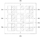
第2実施形態に係る発光素子パッケージは、基板210上に第1発光素子〜第4発光素子250a,250b,250c,250dが配置される。第1発光素子250aは4個の発光セル251a,252a,253a,254aを含み、第2発光素子250bは4個の発光セル251b,252b,253b,254bを含み、第3発光素子250cは4個の発光セル251c,252c,253c,254cを含み、第4発光素子250dは4個の発光セル251d,252d,253d,254dを含むことができる。
In the light emitting device package according to the second embodiment, the first to fourth
第1発光素子〜第4発光素子250a,250b,250c,250dにおいて、一つの発光セル251a,252b,253c,254dは第1蛍光体が配置され、残りの発光セルは第2蛍光体が配置されてもよい。第1蛍光体と第2蛍光体は、それぞれの発光素子250a,250b,250c,250dの活性層から放出される光によって励起されて、それぞれ第1波長領域と第2波長領域の光を放出する。したがって、第1蛍光体が配置された発光セルでは、活性層から放出された光と第1波長領域の光とが混色して外部に放出され、第2蛍光体が配置された発光セルでは、活性層から放出された光と第2波長領域の光とが混色して外部に放出され得る。
In the first to fourth
第3実施形態に係る発光素子パッケージは、基板210上に第1発光素子〜第9発光素子250a〜250iが配置され、発光素子250a〜250iはそれぞれ、4個の発光セルに分かれていてもよい。
In the light emitting device package according to the third embodiment, the first to ninth
それぞれの発光素子250a〜250iの発光セルは、互いに異なる波長領域の光を放出する2種類の発光セルに区分することができ、上述した第2実施形態に係る発光素子パッケージのように、それぞれの発光セルに、互いに異なる波長領域の光を放出する互いに異なる蛍光体を配置することができる。
The light emitting cells of the respective
また、それぞれの発光セルの一部には蛍光体が配置され、残りには蛍光体が配置されなくてもよい。発光セル間の距離が全て同一でなくてもよい。すなわち、同一発光素子内の発光セル間の距離が、隣接する発光素子内の発光セル間の距離よりも小さくてもよい。 Further, the phosphor may be arranged in a part of each light emitting cell and the phosphor may not be arranged in the rest. The distances between the light emitting cells may not all be the same. That is, the distance between the light emitting cells in the same light emitting element may be smaller than the distance between the light emitting cells in the adjacent light emitting elements.
図9に示された実施形態において、それぞれの発光素子250a〜250iの活性層から光が放出されると、上述した活性層から放出された光によって、それぞれの発光セルにおいて蛍光体が励起されて第1波長領域の光と第2波長領域の光を放出し、したがって、一つの発光素子内の発光セルから2種類の光を外部に放出することができる。
In the embodiment shown in FIG. 9, when light is emitted from the active layer of each of the
図8に示された実施形態では、発光素子パッケージ全体から放出される光が特定の形状を示しており、図9に示された実施形態では、発光素子パッケージ全体から放出される光が、数字‘12’の形状を示している。上記のように、発光素子パッケージ内のそれぞれの発光素子を複数個の発光セルに分け、発光セルに互いに異なる種類の蛍光体を配置することで、一つの発光素子ないし発光素子パッケージにおいて様々な形状、例えば、長方形や正方形ではない形状の具現が可能であり、このような形状は、記号、文字または数字などの特定のエンブレム(emblem)をなすことができる。 In the embodiment shown in FIG. 8, the light emitted from the entire light emitting device package has a specific shape, and in the embodiment shown in FIG. 9, the light emitted from the entire light emitting device package is a numeral. The shape of "12" is shown. As described above, by dividing each light emitting device in the light emitting device package into a plurality of light emitting cells and disposing different kinds of phosphors in the light emitting cells, various shapes can be obtained in one light emitting device or a light emitting device package. For example, it is possible to embody a shape other than a rectangle or a square, and such a shape can form a particular emblem such as a symbol, a letter, or a number.
図10A及び図10Bは、発光素子パッケージの第4実施形態、及び点灯と消灯状態を示す図である。 10A and 10B are diagrams illustrating a light emitting device package according to a fourth embodiment and a lighting state and a non-lighting state.
第4実施形態に係る発光素子パッケージは、図8に示された発光素子パッケージと類似している。しかし、図8及び図9において、一つの発光素子は、同一の面積及び形状を有する4個の発光セルからなっているが、本実施形態では、一つの発光素子が4個の発光セルからなり、発光セルの面積及び/または形状が全て同一でなくてもよい。 The light emitting device package according to the fourth embodiment is similar to the light emitting device package shown in FIG. However, in FIG. 8 and FIG. 9, one light emitting device is composed of four light emitting cells having the same area and shape, but in the present embodiment, one light emitting device is composed of four light emitting cells. The area and/or shape of the light emitting cells may not all be the same.
第4実施形態に係る発光素子パッケージは、基板210上に第1発光素子〜第4発光素子250a,250b,250c,250dが配置される。第1発光素子250aは四角形状の2つの発光セル251a,253a及び三角形状の2つの発光セル252a,254aを含み、第2発光素子250bは四角形状の2つの発光セル252b,253b及び三角形状の2つの発光セル251b,254bを含み、第3発光素子250cは四角形状の2つの発光セル251c,253c及び三角形状の2つの発光セル252c,254cを含み、第4発光素子250dは四角形状の2つの発光セル251d,252d及び三角形状の2つの発光セル253d,254dを含むことができる。
In the light emitting device package according to the fourth embodiment, the first to fourth
第1発光素子250a内の一つの発光セル254a、第2発光素子250b内の一つの発光セル254b、第3発光素子250c内の一つの発光セル254c、及び第4発光素子250d内の一つの発光セル254dは、他の発光セルと異なる種類の蛍光体が配置されている。蛍光体の種類が異なるので、発光素子内の活性層から放出された光によって蛍光体が励起されて、異なる波長領域の光を放出し、したがって、上述した4個の発光セル254a,254b,254c,254dから放出される光の波長と、残りの発光セルから放出される光の波長とが互いに異なる。
One
したがって、図10Bに示すように、発光素子に電流が供給されるとき、(a)のように、4個の発光素子によって左側方向の矢印及び/または右側方向の矢印に対応するエンブレムを表示することができる。特に、発光素子パッケージが車両用照明装置に使用されるとき、方向指示エンブレムとして表示され得る。図10Bの(b)は、発光素子に電流が供給されない時を示した図である。 Therefore, as shown in FIG. 10B, when a current is supplied to the light emitting element, the emblem corresponding to the leftward arrow and/or the rightward arrow is displayed by the four light emitting elements as shown in (a). be able to. In particular, when the light emitting device package is used in a vehicle lighting device, it may be displayed as a direction indicating emblem. FIG. 10B(b) is a diagram showing a time when current is not supplied to the light emitting element.
図11A及び図11Bは、発光素子パッケージの第5実施形態、及び点灯と消灯状態を示す図である。 11A and 11B are views showing a fifth embodiment of a light emitting device package and a lighting and extinguishing states.
第5実施形態に係る発光素子パッケージは、上述した第4実施形態と類似しているが、一つの発光素子が、同一の面積及び形状を有する4個の発光セルからなる点で異なる。 The light emitting device package according to the fifth embodiment is similar to the fourth embodiment described above, but is different in that one light emitting device includes four light emitting cells having the same area and shape.
第1発光素子250aは4個の発光セル251a,252a,253a,254aを含み、第2発光素子250bは4個の発光セル251b,252b,253b,254bを含み、第3発光素子250cは4個の発光セル251c,252c,253c,254cを含み、第4発光素子250dは4個の発光セル251d,252d,253d,254dを含むことができる。
The first
第1発光素子〜第4発光素子250a,250b,250c,250dにおいて、一つの発光セル254a,253b,252c,251dは第1蛍光体が配置され、残りの発光セルは第2蛍光体が配置されてもよい。第1蛍光体と第2蛍光体は、それぞれの発光素子250a,250b,250c,250dの活性層から放出される光によって励起されて、それぞれ第1波長領域と第2波長領域の光を放出する。したがって、第1蛍光体が配置された発光セルでは、活性層から放出された光と第1波長領域の光とが混色して外部に放出され、第2蛍光体が配置された発光セルでは、活性層から放出された光と第2波長領域の光とが混色して外部に放出され得る。
In the first to fourth
したがって、図11Bに示すように、発光素子に電流が供給されるとき、(a)のように、内部の4個の発光セルと外部の発光セルとが互いに異なる色を表示することで、特定のエンブレムまたは特定の目的のための表示灯として使用することができ、例えば、車両用照明装置においてブレーキ(break)灯と方向指示灯を一体化させて、選択的又は一体にブレーキ灯と方向指示灯をon/offさせることができる。図11Bの(b)は、発光素子に電流が供給されない時を示した図である。 Therefore, as shown in FIG. 11B, when a current is supplied to the light emitting element, as shown in FIG. 11A, the four light emitting cells inside and the light emitting cells outside are displayed in different colors from each other. It can be used as an emblem of a vehicle or as an indicator light for a specific purpose. For example, in a vehicle lighting device, a brake light and a direction indicator light are integrated to selectively or integrally form a brake light and a direction indicator light. The light can be turned on/off. FIG. 11B(b) is a diagram showing a time when current is not supplied to the light emitting element.
図12A及び図12Bは、発光素子パッケージの発光構造物内の発光セルの構造を示す図である。 12A and 12B are views showing a structure of a light emitting cell in a light emitting structure of a light emitting device package.
図12Aは垂直型発光素子を示し、図12Bは水平型発光素子を示し、それぞれ一つの発光素子内で複数個の発光セルが配置された構造を示している。図12A及び図12Bは、図4でのA−A’方向の垂直方向の断面図である。 12A shows a vertical type light emitting device, and FIG. 12B shows a horizontal type light emitting device, each of which has a structure in which a plurality of light emitting cells are arranged in one light emitting device. 12A and 12B are cross-sectional views taken along the line A-A' in FIG.
図12Aにおいて、基板310上に一つの導電性支持基板340上に2つの発光セル350b,350dが互いに分離されて配置されており、互いに既設定された距離d1だけ離隔している。導電性支持基板340上には導電性のボンディング層342及び第2電極344を配置し、第2電極344上に発光セル350b,350dを配置することができる。
In FIG. 12A, two light emitting
既設定された距離d1は、10μm〜50μmであってもよく、距離が大きすぎると、それぞれの発光セルを別途の発光素子として製造する場合と相違点が少なく、距離が狭すぎると、エッチング工程で分離が難しいことがある。 The preset distance d 1 may be 10 μm to 50 μm. If the distance is too large, there is little difference from the case where each light emitting cell is manufactured as a separate light emitting element, and if the distance is too small, etching is performed. Separation may be difficult in the process.
一つの発光セル350bの上部には第1電極351bを形成し、第1電極351bは基板310上の第1ボンディングパッド310bとワイヤボンディング可能であり、発光セル350bの上部には蛍光体360bを配置することができ、蛍光体360bは、例えば、緑色蛍光体であってもよい。
A
他の発光セル350dの上部には第1電極351dを形成し、第1電極351dは基板310上の第1ボンディングパッド310dとワイヤボンディング可能であり、発光セル350dの上部には蛍光体360dを配置することができ、蛍光体360dは、例えば、黄色蛍光体であってもよい。
A
図12Aの垂直型発光素子において、第1電極は、発光構造物内の第1導電型半導体層上に形成することができる。 In the vertical light emitting device of FIG. 12A, the first electrode may be formed on the first conductive type semiconductor layer in the light emitting structure.
図12Bにおいて、基板310上にサファイアなどからなる絶縁性基板330上に2つの発光セル350b,350dが互いに分離されて配置されており、互いに既設定された距離d1だけ離隔している。
In FIG. 12B, two light emitting
一つの発光セル350bは、一部の領域をメサエッチングし、メサエッチングされた領域に第1電極351bを形成し、発光セル350bの上部には第2電極352bを形成することができ、第1電極351bは基板310上の第1ボンディングパッド310bとワイヤボンディング可能であり、第2電極352bは基板310上の第2ボンディングパッド(図示せず)とワイヤボンディング可能であり、発光セル350bの上部には蛍光体360bを配置することができ、蛍光体360bは、例えば、緑色蛍光体であってもよい。
In one
他の発光セル350dは、一部の領域をメサエッチングし、メサエッチングされた領域に第1電極351dを形成し、発光セル350dの上部には第2電極352dを形成することができ、第1電極351dは基板310上の第1ボンディングパッド310dとワイヤボンディング可能であり、第2電極252dは基板210上の第2ボンディングパッド(図示せず)とワイヤボンディング可能であり、発光セル350dの上部には蛍光体360dを配置することができ、蛍光体360dは、例えば、黄色蛍光体であってもよい。
In the other
図12Bの水平型発光素子において、それぞれの発光セルは、メサエッチングされて第2導電型半導体層から活性層及び第1導電型半導体層の一部がエッチングされることにより、前記第1導電型半導体層の一部が露出され、前記それぞれの領域の発光セルの第2導電型半導体層と露出された第1導電型半導体層上にそれぞれ、第2電極と第1電極を配置することができる。 In the horizontal type light emitting device of FIG. 12B, each light emitting cell is mesa-etched to partially etch the active layer and the first conductive type semiconductor layer from the second conductive type semiconductor layer to thereby obtain the first conductive type. Part of the semiconductor layer is exposed, and the second electrode and the first electrode may be disposed on the second conductive type semiconductor layer of the light emitting cell in the respective regions and the exposed first conductive type semiconductor layer, respectively. ..
上述した発光素子パッケージにおいて、それぞれの発光セルに接続された第1電極と第2電極は、互いに並列に接続されるか、または独立して接続されて、それぞれの発光セルごとに分割して駆動が可能である。そして、図12Aと図12Bなどにおいて、蛍光体はコンフォーマルコーティングされるか、またはフィルムタイプで配置されてもよい。 In the above-described light emitting device package, the first electrode and the second electrode connected to each light emitting cell are connected in parallel with each other or independently and are driven separately for each light emitting cell. Is possible. 12A and 12B, the phosphors may be conformally coated or arranged in a film type.
図13A及び図13Bは、図12A及び図12Bの発光セルの製造工程を示す図であり、図6A及び図6Bに示された実施形態と同一であり得る。図14は、発光素子パッケージが配置された車両用照明装置の一実施形態を示す図である。 13A and 13B are views showing a manufacturing process of the light emitting cell of FIGS. 12A and 12B, and may be the same as the embodiment shown in FIGS. 6A and 6B. FIG. 14: is a figure which shows one Embodiment of the illuminating device for vehicles in which the light emitting element package was arrange|positioned.
実施形態に係る車両用照明装置400は、発光素子パッケージが配置された発光素子モジュール401から放出された光がリフレクタ402とシェード403で反射された後、レンズ404を透過して車体の後方に向かうことができる。発光素子モジュール401は、基板上に上述した発光素子パッケージが配置されてもよい。
In the
上述した車両用照明装置は、発光素子モジュール内のそれぞれの発光素子が複数個の発光セルを含み、一つの発光素子から2つの波長領域の光を放出することができる。 In the above vehicle lighting device, each light emitting element in the light emitting element module includes a plurality of light emitting cells, and one light emitting element can emit light in two wavelength regions.
以上、実施形態を中心に説明したが、これは単なる例示であり、本発明を限定するものではなく、本発明の属する分野における通常の知識を有する者であれば、本実施形態の本質的な特性を逸脱しない範囲で、以上で例示していない様々な変形及び応用が可能であるということが理解されるであろう。例えば、実施形態に具体的に示した各構成要素は変形実施が可能である。そして、このような変形及び応用に係る差異点は、添付の特許請求の範囲で規定する本発明の範囲に含まれるものと解釈しなければならない。 Although the embodiment has been mainly described above, this is merely an example and does not limit the present invention. Any person having ordinary knowledge in the field to which the present invention pertains may have an essential feature of the present embodiment. It will be understood that various modifications and applications not exemplified above are possible without departing from the characteristics. For example, each component specifically shown in the embodiment can be modified. Further, the differences regarding such modifications and applications should be construed to be included in the scope of the present invention defined by the appended claims.
Claims (6)
前記パッケージボディー上に配置され、第1導電型半導体層、活性層及び第2導電型半導体層を含み、複数の発光セル(cell)に分かれた発光構造物と、
前記パッケージボディーと前記発光構造物との間に位置する支持基板と、
前記それぞれの発光セルに接続された第1電極及び第2電極と、
前記それぞれの発光セル上に配置された蛍光体と、を含み、
互いに隣接する発光セルは、前記第1導電型半導体層、前記活性層及び前記第2導電型半導体層のうち少なくとも2層以上が電気的に分離され、
前記蛍光体は、前記複数の発光セルの各々に沿って相互に分離されており、
複数の発光素子の各々が、前記複数の発光セルのうちの対応する複数の発光セルを含み、
前記複数の発光素子の各々に含まれ、或る配線に接続され、第1波長領域の光を放出する第1発光セルと、前記複数の発光素子の各々に含まれ、別の配線に接続され、第2波長領域の光を放出する第2発光セルとが、相互に独立して駆動され、
前記或る配線に接続された複数の前記第1発光セルと前記別の配線に接続された複数の前記第2発光セルとが相互に独立して駆動可能であり、
前記複数の前記第1発光セルの各々が、前記複数の発光素子のうちの該第1発光セルに固有の発光素子に含まれるものであり、
前記複数の前記第2発光セルの各々が、前記複数の発光素子のうちの該第2発光セルに固有の発光素子に含まれるものであり、
前記或る配線に電流が供給されたときに、常に、前記複数の前記第1発光セルが、すべて第1の色の光を放出して、協働して1つの信号を示し、
前記別の配線に電流が供給されたときに、常に、前記複数の前記第2発光セルが、すべて前記第1の色の光とは異なる第2の色の光を放出して、協働して1つの信号を示し、
前記複数の発光素子の各々が、相互に異なる面積及び形状を有する複数の発光セルを含み、
前記形状が矩形及び三角形を含み、
前記それぞれの発光セルは、1つの発光構造物が成長した後、前記成長した1つの発光構造物がエッチングされることにより分かれたものであり、
前記蛍光体は、コンフォーマルコーティングされるか又はフィルムタイプで配置され、
隣接する前記発光セル間の距離は10μm〜50μmであり、
前記複数の発光素子の各々が水平型発光素子又は垂直型発光素子であり、
同一発光素子内の発光セル間の距離が、隣接する発光素子内の発光セル間の距離よりも小さい、発光素子パッケージ。 Package body,
A light emitting structure disposed on the package body, the light emitting structure including a first conductive type semiconductor layer, an active layer, and a second conductive type semiconductor layer and divided into a plurality of light emitting cells.
A support substrate located between the package body and the light emitting structure;
A first electrode and a second electrode connected to each of the light emitting cells;
And a phosphor disposed on each of the light emitting cells,
In the light emitting cells adjacent to each other, at least two layers of the first conductive type semiconductor layer, the active layer, and the second conductive type semiconductor layer are electrically separated.
The phosphors are separated from each other along each of the plurality of light emitting cells,
Each of the plurality of light emitting elements includes a plurality of corresponding light emitting cells of the plurality of light emitting cells,
A first light emitting cell included in each of the plurality of light emitting elements and connected to a certain wiring to emit light in a first wavelength region; and a first light emitting cell included in each of the plurality of light emitting elements and connected to another wiring , A second light emitting cell that emits light in the second wavelength region is driven independently of each other,
A plurality of the first light emitting cells connected to the certain wiring and a plurality of the second light emitting cells connected to the other wiring can be independently driven.
Each of the plurality of first light emitting cells is included in a light emitting element unique to the first light emitting cell among the plurality of light emitting elements,
Each of the plurality of second light emitting cells is included in a light emitting element unique to the second light emitting cell among the plurality of light emitting elements,
When a current is supplied to the certain wiring, the plurality of first light emitting cells all emit light of the first color and cooperate with each other to present one signal.
When a current is supplied to the other wiring, the plurality of second light emitting cells all emit a second color light different from the first color light to cooperate with each other. Shows one signal,
Each of the plurality of light emitting devices includes a plurality of light emitting cells having different areas and shapes,
The shape includes a rectangle and a triangle,
Each of the light emitting cells is divided by growing one light emitting structure and then etching the grown one light emitting structure.
The phosphor is conformally coated or arranged in a film type,
The distance between the adjacent light emitting cells is 10 μm to 50 μm,
Each of the plurality of light emitting devices is a horizontal light emitting device or a vertical light emitting device,
A light emitting device package in which a distance between light emitting cells in the same light emitting device is smaller than a distance between light emitting cells in adjacent light emitting devices.
Applications Claiming Priority (4)
| Application Number | Priority Date | Filing Date | Title |
|---|---|---|---|
| KR20130103830A KR20150025797A (en) | 2013-08-30 | 2013-08-30 | Light emitting device package and lighting device including the same for vehicle |
| KR10-2013-0103830 | 2013-08-30 | ||
| KR1020130103831A KR102080776B1 (en) | 2013-08-30 | 2013-08-30 | Light emitting device package and lighting device including the same for vehicle |
| KR10-2013-0103831 | 2013-08-30 |
Publications (3)
| Publication Number | Publication Date |
|---|---|
| JP2015050461A JP2015050461A (en) | 2015-03-16 |
| JP2015050461A5 JP2015050461A5 (en) | 2017-10-05 |
| JP6713720B2 true JP6713720B2 (en) | 2020-06-24 |
Family
ID=51417223
Family Applications (1)
| Application Number | Title | Priority Date | Filing Date |
|---|---|---|---|
| JP2014173374A Active JP6713720B2 (en) | 2013-08-30 | 2014-08-28 | Light emitting device package and vehicle lighting device including the same |
Country Status (4)
| Country | Link |
|---|---|
| US (1) | US9269861B2 (en) |
| EP (1) | EP2843705B1 (en) |
| JP (1) | JP6713720B2 (en) |
| CN (1) | CN104425540A (en) |
Families Citing this family (8)
| Publication number | Priority date | Publication date | Assignee | Title |
|---|---|---|---|---|
| CN111490146A (en) | 2014-11-18 | 2020-08-04 | 首尔半导体株式会社 | Light emitting device |
| US10170455B2 (en) * | 2015-09-04 | 2019-01-01 | PlayNitride Inc. | Light emitting device with buffer pads |
| TWI646706B (en) * | 2015-09-21 | 2019-01-01 | 隆達電子股份有限公司 | Led chip package |
| US10219345B2 (en) * | 2016-11-10 | 2019-02-26 | Ledengin, Inc. | Tunable LED emitter with continuous spectrum |
| KR102563894B1 (en) | 2017-02-08 | 2023-08-10 | 서울반도체 주식회사 | Light emitting diode and light emitting module comprising the same |
| JP6986697B2 (en) * | 2017-06-28 | 2021-12-22 | パナソニックIpマネジメント株式会社 | Ultraviolet light emitting element |
| US10340308B1 (en) | 2017-12-22 | 2019-07-02 | X Development Llc | Device with multiple vertically separated terminals and methods for making the same |
| KR102642606B1 (en) | 2019-05-30 | 2024-03-05 | 삼성디스플레이 주식회사 | Window and manufacturing method for the same |
Family Cites Families (24)
| Publication number | Priority date | Publication date | Assignee | Title |
|---|---|---|---|---|
| JPH09330604A (en) * | 1996-06-06 | 1997-12-22 | Koito Mfg Co Ltd | Marker lamp for vehicle |
| JP3691951B2 (en) * | 1998-01-14 | 2005-09-07 | 東芝電子エンジニアリング株式会社 | Gallium nitride compound semiconductor light emitting device |
| US6404125B1 (en) * | 1998-10-21 | 2002-06-11 | Sarnoff Corporation | Method and apparatus for performing wavelength-conversion using phosphors with light emitting diodes |
| US6737801B2 (en) * | 2000-06-28 | 2004-05-18 | The Fox Group, Inc. | Integrated color LED chip |
| JP2004055742A (en) * | 2002-07-18 | 2004-02-19 | Sanyo Electric Co Ltd | Light-emitting device and light-emitting device array equipped with same |
| US7675075B2 (en) | 2003-08-28 | 2010-03-09 | Panasonic Corporation | Semiconductor light emitting device, light emitting module, lighting apparatus, display element and manufacturing method of semiconductor light emitting device |
| WO2006095949A1 (en) * | 2005-03-11 | 2006-09-14 | Seoul Semiconductor Co., Ltd. | Led package having an array of light emitting cells coupled in series |
| JP2009224431A (en) * | 2008-03-14 | 2009-10-01 | Nichia Corp | Semiconductor device |
| WO2010020068A1 (en) * | 2008-08-19 | 2010-02-25 | Lattice Power (Jiangxi) Corporation | Semiconductor light-emitting devices for generating arbitrary color |
| KR101154758B1 (en) * | 2008-11-18 | 2012-06-08 | 엘지이노텍 주식회사 | Semiconductor light emitting device and LED package having the same |
| KR101562774B1 (en) | 2009-02-24 | 2015-10-22 | 서울반도체 주식회사 | Light emitting module |
| TWI381556B (en) * | 2009-03-20 | 2013-01-01 | Everlight Electronics Co Ltd | Light emitting diode package structure and manufacturing method thereof |
| US8455904B2 (en) * | 2009-04-20 | 2013-06-04 | 3M Innovative Properties Company | Non-radiatively pumped wavelength converter |
| KR101007077B1 (en) * | 2009-11-06 | 2011-01-10 | 엘지이노텍 주식회사 | Light emitting device, light emitting device package and method for fabricating the same |
| EP2367203A1 (en) * | 2010-02-26 | 2011-09-21 | Samsung LED Co., Ltd. | Semiconductor light emitting device having multi-cell array and method for manufacturing the same |
| US8604498B2 (en) * | 2010-03-26 | 2013-12-10 | Tsmc Solid State Lighting Ltd. | Single phosphor layer photonic device for generating white light or color lights |
| JP2012019104A (en) | 2010-07-08 | 2012-01-26 | Mitsubishi Chemicals Corp | Light emitting apparatus |
| CN103180945B (en) * | 2010-10-27 | 2016-12-07 | 皇家飞利浦电子股份有限公司 | For manufacturing lamination support membrane and the manufacture method thereof of luminescent device |
| EP2660882B1 (en) * | 2010-12-28 | 2018-10-03 | Nichia Corporation | Semiconductor light-emitting device |
| KR101748334B1 (en) * | 2011-01-17 | 2017-06-16 | 삼성전자 주식회사 | Apparatus and method of fabricating white light emitting device |
| JP2012216712A (en) * | 2011-03-28 | 2012-11-08 | Nitto Denko Corp | Method for manufacturing light-emitting diode device and light-emitting element |
| US20130075769A1 (en) | 2011-09-22 | 2013-03-28 | Ledengin, Inc. | Selection of phosphors and leds in a multi-chip emitter for a single white color bin |
| TW201320406A (en) * | 2011-11-11 | 2013-05-16 | Unity Opto Technology Co Ltd | Improved white LED packaging structure for improving light mixing effect |
| KR102003001B1 (en) | 2013-03-13 | 2019-07-23 | 엘지이노텍 주식회사 | Light emitting module |
-
2014
- 2014-08-28 JP JP2014173374A patent/JP6713720B2/en active Active
- 2014-08-29 CN CN201410437156.6A patent/CN104425540A/en active Pending
- 2014-08-29 US US14/472,514 patent/US9269861B2/en active Active
- 2014-08-29 EP EP14182912.7A patent/EP2843705B1/en active Active
Also Published As
| Publication number | Publication date |
|---|---|
| JP2015050461A (en) | 2015-03-16 |
| CN104425540A (en) | 2015-03-18 |
| US9269861B2 (en) | 2016-02-23 |
| EP2843705A1 (en) | 2015-03-04 |
| US20150062949A1 (en) | 2015-03-05 |
| EP2843705B1 (en) | 2020-03-11 |
Similar Documents
| Publication | Publication Date | Title |
|---|---|---|
| JP6713720B2 (en) | Light emitting device package and vehicle lighting device including the same | |
| US8264142B2 (en) | Illumination apparatus and method of producing a planar light output | |
| CN112136219B (en) | Lighting module | |
| CN208959334U (en) | Light emitting device and vehicle lamp including the light emitting device | |
| TWI546984B (en) | Light emitting device module | |
| TWI610465B (en) | Light-emitting diode assembly and manufacturing method thereof | |
| KR20070102425A (en) | Semiconductor light-emitting device and method of fabricating the same | |
| JP2011040263A (en) | Light-emitting device and method of manufacturing the same, lamp, and lamp system | |
| US9825206B2 (en) | Light-emitting device | |
| KR20150113183A (en) | Light-emitting module | |
| KR102080776B1 (en) | Light emitting device package and lighting device including the same for vehicle | |
| US20210296530A1 (en) | Vehicular display element comprising high density mini-pixel led array | |
| KR20150025797A (en) | Light emitting device package and lighting device including the same for vehicle | |
| JP4749975B2 (en) | Light emitting diode package structure | |
| JP2007176219A (en) | Light emission device, and vehicular light using the same | |
| CN108109534B (en) | Pixel light emitting device | |
| KR100609970B1 (en) | Substrate for mounting light emitting device, fabricating method thereof and package using the same | |
| KR100523740B1 (en) | Lamp utilizing the LED | |
| US10480760B2 (en) | Light source module | |
| TWI608601B (en) | Led module, led array module and display module | |
| KR102209035B1 (en) | Light emitting device package | |
| CN220774405U (en) | Porous fluorescent sheet and high-brightness LED module and chip | |
| KR20120018846A (en) | Light emitting device and method for fabricating the same | |
| KR101797595B1 (en) | light emitting device package | |
| KR20110131444A (en) | A color filter and a backlight unit including the color filter |
Legal Events
| Date | Code | Title | Description |
|---|---|---|---|
| A521 | Request for written amendment filed |
Free format text: JAPANESE INTERMEDIATE CODE: A523 Effective date: 20170825 |
|
| A621 | Written request for application examination |
Free format text: JAPANESE INTERMEDIATE CODE: A621 Effective date: 20170825 |
|
| A977 | Report on retrieval |
Free format text: JAPANESE INTERMEDIATE CODE: A971007 Effective date: 20180620 |
|
| A131 | Notification of reasons for refusal |
Free format text: JAPANESE INTERMEDIATE CODE: A131 Effective date: 20180731 |
|
| A521 | Request for written amendment filed |
Free format text: JAPANESE INTERMEDIATE CODE: A523 Effective date: 20181023 |
|
| A131 | Notification of reasons for refusal |
Free format text: JAPANESE INTERMEDIATE CODE: A131 Effective date: 20190326 |
|
| A521 | Request for written amendment filed |
Free format text: JAPANESE INTERMEDIATE CODE: A523 Effective date: 20190614 |
|
| A131 | Notification of reasons for refusal |
Free format text: JAPANESE INTERMEDIATE CODE: A131 Effective date: 20191126 |
|
| A521 | Request for written amendment filed |
Free format text: JAPANESE INTERMEDIATE CODE: A523 Effective date: 20191220 |
|
| TRDD | Decision of grant or rejection written | ||
| A01 | Written decision to grant a patent or to grant a registration (utility model) |
Free format text: JAPANESE INTERMEDIATE CODE: A01 Effective date: 20200519 |
|
| A61 | First payment of annual fees (during grant procedure) |
Free format text: JAPANESE INTERMEDIATE CODE: A61 Effective date: 20200604 |
|
| R150 | Certificate of patent or registration of utility model |
Ref document number: 6713720 Country of ref document: JP Free format text: JAPANESE INTERMEDIATE CODE: R150 |
|
| R250 | Receipt of annual fees |
Free format text: JAPANESE INTERMEDIATE CODE: R250 |